WO2018074274A1 - 電力変換装置および空気調和機 - Google Patents
電力変換装置および空気調和機 Download PDFInfo
- Publication number
- WO2018074274A1 WO2018074274A1 PCT/JP2017/036552 JP2017036552W WO2018074274A1 WO 2018074274 A1 WO2018074274 A1 WO 2018074274A1 JP 2017036552 W JP2017036552 W JP 2017036552W WO 2018074274 A1 WO2018074274 A1 WO 2018074274A1
- Authority
- WO
- WIPO (PCT)
- Prior art keywords
- switching element
- switching
- leg
- control
- current
- Prior art date
- Legal status (The legal status is an assumption and is not a legal conclusion. Google has not performed a legal analysis and makes no representation as to the accuracy of the status listed.)
- Ceased
Links
Images









Classifications
-
- F—MECHANICAL ENGINEERING; LIGHTING; HEATING; WEAPONS; BLASTING
- F24—HEATING; RANGES; VENTILATING
- F24F—AIR-CONDITIONING; AIR-HUMIDIFICATION; VENTILATION; USE OF AIR CURRENTS FOR SCREENING
- F24F11/00—Control or safety arrangements
- F24F11/70—Control systems characterised by their outputs; Constructional details thereof
- F24F11/80—Control systems characterised by their outputs; Constructional details thereof for controlling the temperature of the supplied air
- F24F11/86—Control systems characterised by their outputs; Constructional details thereof for controlling the temperature of the supplied air by controlling compressors within refrigeration or heat pump circuits
-
- H—ELECTRICITY
- H02—GENERATION; CONVERSION OR DISTRIBUTION OF ELECTRIC POWER
- H02M—APPARATUS FOR CONVERSION BETWEEN AC AND AC, BETWEEN AC AND DC, OR BETWEEN DC AND DC, AND FOR USE WITH MAINS OR SIMILAR POWER SUPPLY SYSTEMS; CONVERSION OF DC OR AC INPUT POWER INTO SURGE OUTPUT POWER; CONTROL OR REGULATION THEREOF
- H02M7/00—Conversion of AC power input into DC power output; Conversion of DC power input into AC power output
- H02M7/02—Conversion of AC power input into DC power output without possibility of reversal
- H02M7/04—Conversion of AC power input into DC power output without possibility of reversal by static converters
- H02M7/12—Conversion of AC power input into DC power output without possibility of reversal by static converters using discharge tubes with control electrode or semiconductor devices with control electrode
Definitions
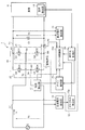
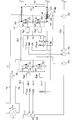
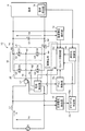
- FIG. 1 is an overall block diagram of a power conversion device 1 according to the first embodiment.
- the power conversion device 1 is a converter that converts an AC power supply voltage Vs applied from an AC power supply G into a DC voltage Vd, and outputs the DC voltage Vd to a load H (an inverter, a motor, etc.).
- the power conversion device 1 has an input side connected to the AC power supply G and an output side connected to the load H.
- the power conversion device 1 includes a bridge circuit 10, a reactor L ⁇ b> 1, a smoothing capacitor C ⁇ b> 1, a current detection unit 11, an AC voltage detection unit 12, a DC voltage detection unit 13, and a load detection unit. 14, a shunt resistor R ⁇ b> 1, and a control unit 15.
- the bridge circuit 10 includes a switching element Q1 (first switching element), a switching element Q2 (second switching element), a switching element Q3 (third switching element), and a switching element Q4 (fourth switching element). I have.
- the bridge circuit 10 has an input side connected to an AC power source G and an output side connected to a load H.
- the switching elements Q1 to Q4 of the bridge circuit 10 are connected in a bridge shape as shown in FIG.
- the switching elements Q1 to Q4 are, for example, MOSFETs (Metal-Oxide-Semiconductor Field-Effect Transistors), and are turned on / off by the control unit 15. Use of MOSFETs as the switching elements Q1 to Q4 has advantages that switching loss can be reduced and switching can be performed at high speed.
- the switching element Q1 has a parasitic diode D1 therein.
- the parasitic diode D1 is a pn junction portion that exists between the source and drain of the switching element Q1.
- the saturation voltage (drain-source voltage in the on state) of the switching element Q1 is preferably lower than the voltage drop in the forward direction of the parasitic diode D1. This is because the voltage drop is smaller when the current is passed through the source / drain of the switching element Q1 than when the current is passed through the parasitic diode D1, thereby reducing the conduction loss. In other words, the conduction loss is smaller when a current is passed through the switching element Q1 in the on state than when a current is passed through the parasitic diode D1 in the switching element Q1 in the off state. The same applies to the other switching elements Q2 to Q4.
- the reverse recovery time (trr) of the parasitic diodes of the switching elements Q1 and Q2 used in this embodiment is relatively shorter than the reverse recovery times of the parasitic diodes of the switching elements Q3 and Q4. This is because the switching elements Q1 and Q2 generate a reverse recovery current in the parasitic diode during the power factor correction operation described later, so that the switching elements Q1 and Q2 are relatively parasitic diodes relative to the switching elements Q3 and Q4. This is because switching loss is reduced by using an element having a short reverse recovery time.
- connection point N2 is connected to the AC power supply G via the wiring hb.
- the wiring hb has one end connected to the AC power supply G and the other end connected to the connection point N2 described above.
- the drain of the switching element Q1 and the drain of the switching element Q3 are connected to each other, and the connection point N3 is connected to the load H through the wiring hc.
- the wiring hc has one end connected to the load H and the other end connected to the connection point N3 described above.
- the source of the switching element Q2 and the source of the switching element Q4 are connected to each other, and the connection point N4 is connected to the load H through the wiring hd.
- the wiring hd has one end connected to the sources of the switching elements Q2 and Q4 and the other end connected to the load H.
- the current detection unit 11 detects the current flowing through the bridge circuit 10 as an effective value (average current), and is provided in the wiring hb.
- a current transformer can be used as the current detection unit 11, for example.
- the AC voltage detector 12 detects an AC power supply voltage vs (instantaneous value) applied from the AC power supply G, and is connected to the wirings ha and hb.
- the DC voltage detector 13 detects the DC voltage Vd of the smoothing capacitor C1, and its positive side is connected to the wiring hc and its negative side is connected to the wiring hd. Note that the detection value of the DC voltage detection unit 13 is used to determine whether or not the voltage value applied to the load H has reached a predetermined target value.
- the zero cross determiner 15a determines whether the polarity of the AC power supply voltage vs has been switched, that is, whether the zero cross timing has been reached. For example, the zero-cross determination unit 15a outputs a signal “1” to the converter control unit 15d while the AC power supply voltage vs is positive, and outputs a signal “1” to the converter control unit 15d while the AC power supply voltage vs is negative. A 0 'signal is output.
- the step-up ratio control unit 15b has a function of setting the step-up ratio of the DC voltage Vd based on the detection value of the current detection unit 11, and outputting the step-up ratio to the gain control unit 15c and the converter control unit 15d. .
- the gain control unit 15c has a function of setting a current control gain based on the effective value of the circuit current is detected by the current detection unit 11 and the step-up ratio of the DC voltage Vd.
- Vcc is a connection terminal for driving power supply voltage of IC1 and IC2.
- HIN is connected to the output ports P1 and P5 of the converter control unit 15d. When a signal is input from the converter control unit 15d, a drive signal for driving the high-side switching elements Q1 and Q3 is output from the HO terminal.
- LIN is connected to the output ports P2 and P6 of the converter control unit 15d, and when a signal is input from the converter control unit 15d, a drive signal for driving the low-side switching elements Q2 and Q4 is output from the LO terminal. Is done.
- the Vs terminals of the drive circuits IC1 and IC2 are connected to the connection points N1 and N2, respectively.
- the GND terminal is connected to the connection point N5 on the wiring hd on the negative electrode side of the smoothing capacitor C1.
- the ITrip terminal is connected to a connection point N6 having the same potential as the drains of the switching elements Q2 and Q4.
- the Fault terminal is connected to the input port P4 of the converter control unit 15d via the connection point N7.
- the shunt resistor R1 is connected to the input port P3 of the converter control unit 15d.
- Diode rectification control is a control mode in which full-wave rectification is performed using four parasitic diodes D1 to D4. The diode rectification control is executed, for example, when the load is relatively small, but is not limited thereto.
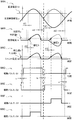
- FIG. 3 is a waveform diagram showing temporal changes in the AC power supply voltage vs, the circuit current is, and the drive pulses of the switching elements Q1 to Q4 in the diode rectification control.
- Waveform W3A is a waveform of AC power supply voltage vs (instantaneous value)
- waveform W3B is a waveform of circuit current is (instantaneous value).
- Waveforms W3C, W3D, W3E, and W3F are waveforms of drive pulses for switching elements Q1 to Q4. As shown by the waveforms W3C, W3D, W3E, and W3F in FIG. 3, the converter control unit 15d maintains all of the switching elements Q1 to Q4 in an off state, so that parasitic diodes D1 to D4 are described as described below. Through the circuit current is.
- the circuit is in the order of AC power supply G ⁇ parasitic diode D3 ⁇ smoothing capacitor C1 ⁇ shunt resistor R1 ⁇ parasitic diode D2 ⁇ reactor L1 ⁇ AC power supply G.
- a current is flows.
- the waveform of the circuit current is as shown by the waveform W3B in FIG.
- FIG. 5 is an explanatory diagram showing a current flow when the AC power supply voltage vs is included in the positive half cycle in the synchronous rectification control.
- the AC power supply G ⁇ reactor L1 ⁇ switching element Q1 ⁇ smoothing capacitor C1 ⁇ shunt resistor R1 ⁇ switching element Q4 ⁇ AC power supply G as shown by the broken line arrow in FIG.
- the circuit current is flows in the current path.
- the current path of the AC power supply G ⁇ switching element Q3 ⁇ smoothing capacitor C1 ⁇ shunt resistor R1 ⁇ switching element Q2 ⁇ reactor L1 ⁇ AC power supply G
- the circuit current is flows in FIG.
- the switching elements Q1 to Q4 are subjected to switching control in synchronization with the polarity of the power supply voltage, so that a current is actively supplied to the portion of the on-resistance having a small loss, and the parasitic diodes D1 to D4 are passed through. , Almost no current flow.
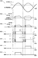
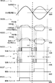
- FIG. 6 is an explanatory diagram showing temporal changes in the AC power supply voltage vs, the circuit current is, the current sh flowing through the shunt resistor R1, and the driving pulses of the switching elements Q1 to Q4 in the synchronous rectification control.
- converter control unit 15d switches on / off switching elements Q1-Q4 in synchronization with circuit current is.
- a description will be given by taking as an example a section in which the AC power supply voltage vs is a positive half cycle.
- the zero cross of the AC power supply voltage is detected by the AC voltage detection unit 12 and the zero cross determination unit 15a.
- the circuit current Is starts to flow after a lapse of a certain time from the zero cross of the AC power supply voltage.
- the circuit current is begins to flow when the AC power supply voltage vs increases and becomes equal to the DC voltage Vd, and then the time dt1 further elapses. Then, after the DC voltage Vd becomes equal to the AC voltage again, the circuit current becomes zero after a further time dt2. That is, a current flows when the DC voltage Vd is larger than the AC power supply voltage vs. On the contrary, when the DC voltage Vd is larger than the AC power supply voltage vs, the circuit current is does not flow.
- time delays dt1 and dt2 occur as described above. These phenomena are caused by a time delay caused by the reactor L1.
- the time dt2 is expressed by the following (Formula 1).
- the converter control unit 15d When the AC power supply voltage vs has a positive polarity, the converter control unit 15d first inputs a drive pulse to the gate of the switching element Q1 at the zero-cross timing to turn on the switching element Q1. Thereafter, the circuit current is> 0, and a drive pulse is input to the gate of the switching element Q4 at a predetermined timing to turn on the switching element Q4. Next, a method for driving the switching element Q4 will be described.
- the timing for turning on / off the switching element Q4 is determined by the detected value of the current ish (hereinafter referred to as shunt current) detected by the shunt resistor R1.
- shunt current the detected value of the current ish
- Two current determination values that is, a determination value a (first determination threshold value) and a determination value b (second determination threshold value) are stored in advance in the converter control unit 15d.
- converter control unit 15d inputs a drive pulse to switching element Q4 at the timing when shunt current ish becomes equal to or greater than determination value a, and turns on switching element Q4. Thereafter, converter control unit 15d turns off switching element Q4 at the timing when the circuit current becomes equal to or less than determination value b.
- the power conversion device 1 of the present embodiment shifts the timing for turning on the switching elements Q1 and Q4 when performing synchronous rectification. That is, when the AC power supply voltage vs has a positive polarity, the switching element Q4 is turned on after a predetermined time has elapsed since the switching element Q1 was turned on. This is to prevent backflow of current from the smoothing capacitor C1, that is, the DC voltage side to the AC power supply.
- FIG. 7 is a characteristic diagram showing the relationship between the drain reverse currents of the switching elements Q1 and Q4 and the saturation voltage of the parasitic diode.
- the drain reverse current means a current that flows from the source to the drain of the switching element.
- the parasitic diode saturation voltage means a voltage drop generated in the parasitic diode when a drain reverse current flows through the parasitic diode.
- the reverse recovery time of the parasitic diode D1 of the switching element Q1 is relatively small with respect to the reverse recovery time of the parasitic diode D4 of the switching element Q4.
- the saturation voltages of the respective parasitic diodes have a relationship as shown in FIG.
- the drain reverse current “small” region is a light load region that is not normally used by the device including the power conversion device 1
- the drain reverse current “medium” region is the power conversion device. 1 is a region used by the normal operation operation, and a region where the drain reverse current is “large” means a region used by the device including the power converter 1 in the overload operation.
- the switching element Q ⁇ b> 1 is turned on in the section of time dt ⁇ b> 3 from when the circuit current is starts to flow until the switching element Q ⁇ b> 4 is turned on.
- the circuit current is flows through the on-resistance portion with a small loss.
- the switching element Q4 since the switching element Q4 is turned off, the circuit current is flows through the parasitic diode D4. That is, the loss (area S) generated at time dt3 is the total value of the conduction loss caused by the on-resistance of switching element Q1 and the conduction loss caused by the parasitic diode of switching element Q4.
- the switching element Q4 is turned on first, and the switching element Q1 is turned on when the circuit current is and the shunt current ish reach the judgment value a.
- the loss in the area S is the sum of the conduction loss in the on-resistance portion of the switching element Q4 and the parasitic diode of the switching element Q1.
- the conduction loss of the parasitic diode of the switching element Q1 is larger than the conduction loss of the parasitic diode of the switching element Q4. For this reason, the loss in the area S is increased as compared with the case of switching in the order of the switching elements Q1 ⁇ Q4.
- the switching elements Q3 and Q4 use elements having different characteristics from the switching elements Q1 and Q2.
- the reverse recovery time of the parasitic diodes of the switching elements Q1, Q2 is relatively shorter than the reverse recovery time of the parasitic diodes of the switching elements Q3, Q4.
- the saturation voltage Vf of the parasitic diodes of the switching elements Q1, Q2 is relatively higher than the saturation voltage Vf of the parasitic diodes of the switching elements Q3, Q4.
- the switching elements on the side connected to the reactor L1 after the zero cross detection that is, the element switching elements Q1, Q2 having a high saturation voltage Vf of the parasitic diode are turned on first.
- the switching elements Q3 and Q4 on the side that is not connected to the reactor, that is, the low saturation voltage of the parasitic diode are turned on. .
- the switching elements Q1, Q2 are switched on / off at the zero cross timing at which the AC power supply voltage vs switches from positive to negative.
- a dead time td during which both switching elements Q1 and Q2 are turned off is provided.
- the partial switching control is a control mode in which an operation for short-circuiting the reactor L1 by alternately turning on / off the two switching elements Q1 and Q2 connected to the reactor L1 among the switching elements Q1 to Q4 is performed a predetermined number of times. By such control, it is possible to reduce the harmonic current by improving the power source power factor and boost the DC voltage.
- FIG. 8 is an explanatory diagram showing temporal changes in the AC power supply voltage vs, the circuit current is, the current ish flowing through the shunt resistor R1, and the driving pulses of the switching elements Q1 to Q4 in the partial switching control.
- FIG. 8 shows an example in which the reactor L1 is short-circuited only twice per shot, that is, half a cycle.
- the converter control unit 15d turns on / off the switching elements Q1 and Q2 alternately at a predetermined number of times and with a predetermined pulse width. That is, converter control unit 15d operates to turn on / off switching elements Q1 and Q2 alternately as shown by waveforms W8D and W8E in FIG. 8 immediately after the zero cross timing at which the positive / negative of AC power supply voltage vs is switched. Is performed a predetermined number of times. Further, as shown by waveforms W8F and W8G, converter control unit 15d sets on / off states of switching elements Q3 and Q4 in synchronization with the polarity of AC power supply voltage vs.
- FIG. 9 is an explanatory diagram showing the flow of current when the power factor correction operation is performed in a half cycle in which the AC power supply voltage vs is positive polarity.
- the AC power supply G ⁇ reactor L1 ⁇ switching element Q2 ⁇ switching element Q4 ⁇ AC power supply G is short-circuited, as shown by the dashed arrow in FIG.
- the power factor correction current isp flows. Since the switching element Q4 is assumed to be in a synchronous live operation described later, the short circuit current isp flows through the on-resistance portion, not the parasitic diode D4. At this time, the energy represented by the following (Equation 2) is stored in the reactor L1. Note that I sp shown in (Expression 2) is an effective value of the short-circuit current isp.
- the converter control unit 15d performs the “synchronous rectification operation”. That is, converter control unit 15d switches switching element Q1 from off to on (see waveform W8D in FIG. 8), and switches switching element Q2 from on to off (see waveform W8E in FIG. 8). During this period, the switching element Q3 is maintained in the off state (see waveform W8F in FIG. 8).
- FIG. 8 is a diagram illustrating the case of 2 shots (when the power factor improvement operation is performed twice), but 3 shots (the power factor improvement operation is performed 3 times), 4 shots (power factor improvement operation 4)
- the number of power factor improvement operations may be increased.
- the short-circuit current isp in FIG. 9 also during the power factor correction operation by the switching element Q2.
- the current flows not to the parasitic diode D4 of the switching element Q4 but to the on-resistance portion, high-efficiency operation is possible.
- the converter control unit 15d turns on the switching elements Q1 and Q4 in the section in which the circuit current is flows. Therefore, since the conduction loss between the switching elements Q1 and Q4 can be reduced, high-efficiency operation is possible.
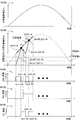
- FIG. 10 is an explanatory diagram of partial switching control in a half cycle in which the AC power supply voltage vs is positive.
- the horizontal axis in FIG. 10 is time.
- a waveform W10A in FIG. 10 shows the AC power supply voltage vs in the positive half cycle.
- a waveform W10B in FIG. 10 is a circuit current is, a short-circuit current isp, and a sinusoidal ideal current.
- Waveforms W10C, W10D, and W10E in FIG. 10 are drive pulses for the switching elements Q2, Q4, and Q1. As shown in the “ideal current” of the waveform W10B in FIG. 10, it is ideal that the sine wave circuit current is flows in phase with the AC power supply voltage vs.
- the switching element Q2 when the switching element Q2 is off, the synchronous rectification operation is performed with the switching element Q1 in the on state, so that high-efficiency operation is possible.
- the switching element Q4 when the power factor correction operation is not performed as described above, synchronous rectification is performed by turning on the switching element Q4 at a timing when the detection value of the shunt current ish exceeds the determination value a. High-efficiency operation is possible.
- a dead time is provided for a predetermined time in order to prevent a vertical short circuit of the smoothing capacitor C1.
- the switching elements Q1 and Q2 are turned on / off alternately (see waveforms W11D and W11E). Further, in synchronization with the polarity of the AC power supply voltage vs, the switching element Q3 is turned on (see waveform W11F) and the switching element Q4 is turned off (see waveform W11G). Note that the on-duty of the switching elements Q1, Q2 is appropriately set so that the circuit current is approximates a sine wave.
- the circuit current is (instantaneous value) in the power conversion device 1 is expressed by the following (Equation 3).
- Vs is an effective value of the AC power supply voltage vs
- Kp is a current control gain
- Vd is a DC voltage
- ⁇ is an angular frequency.
- circuit current is (instantaneous value) and the circuit current Is (effective value) is expressed by the following (Equation 5).
- the circuit current is (instantaneous value) is detected by the shunt resistor R1
- the circuit current Is (effective value) is detected by the current detector 11.
- the on-duty d (conduction ratio) of the switching element Q2 is expressed by the following (Equation 8). The same applies to the on-duty d of the switching element Q1 in the half cycle in which the AC power supply voltage vs is negative.
- the DC voltage Vd can be boosted to a times the AC power supply voltage Vs (effective value) by controlling Kp ⁇ Is shown in (Equation 7).
- the on-duty d of the switching element Q2 (or the switching element Q1) at that time is given by the above (Formula 8).
- the boost ratio m is set by the boost ratio control unit 15b (see FIG. 9) based on the load detected by the load detection unit 14. For example, the step-up ratio m is set to a larger value as the load is larger.
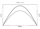
- FIG. 12 is an explanatory diagram showing the on-duty of the switching elements Q1, Q2 in the high-speed switching control in the half cycle in which the AC power supply voltage vs is positive.
- the horizontal axis in FIG. 12 represents the time in the positive half cycle of the AC power supply voltage vs (the elapsed time from the start of the positive half cycle), and the vertical axis represents the on-duty d_Q1, switching elements Q1, Q2. d_Q2.
- the broken line in FIG. 12 is the on-duty d_Q1 of the switching element Q1 when the dead time dtx is not considered.
- the solid line is the on-duty d_Q1 of the switching element Q1 when the dead time dtx is considered.
- a two-dot chain line is the on-duty d_Q2 of the switching element Q2.
- the on-duty d_Q1 of the switching element Q1 indicated by the broken line is set to be proportional to the AC power supply voltage Vs (effective value), for example.
- the on-duty d_Q2 of the switching element Q2 indicated by the two-dot chain line is set as a value obtained by subtracting the on-duty d_Q1 of the switching element Q1 from 1.0.
- the AC power supply voltage vs and the circuit current is have a sine wave waveform, and the AC power supply voltage vs and the circuit current is are substantially in phase. That is, it can be seen that the power factor is improved by performing high-speed switching control.
- the on-duty d_Q2 of the switching element Q2 is set by the following (Equation 9).
- the on-duty d_Q1 of the switching element Q1 is set by the following (Equation 10).
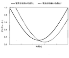
- FIG. 14 is an explanatory diagram showing the on-duty d_Q2 of the switching element Q2 when the current phase delay due to the reactor L1 is not considered and when the current phase delay is considered in the high-speed switching control.
- the horizontal axis in FIG. 14 is the elapsed time (time) from the start of the positive half cycle of the AC power supply voltage vs, and the vertical axis is the on-duty of the switching element Q2 in the high-speed switching control.
- the solid line is the on-duty of the switching element Q2 when the current phase delay due to the reactor L1 is not taken into consideration.
- a broken line is the on-duty of the switching element Q2 when the delay of the current phase due to the reactor L1 is taken into consideration. As shown by the broken line in FIG. 14, by setting the on-duty of the switching element Q2, a sine-wave circuit current is can flow even when the inductance of the reactor L1 is large.
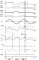
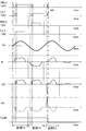
- FIG. 15 is an explanatory diagram in a case where overcurrent flows when performing synchronous rectification control and protection control is performed.
- a waveform HIN_1 in the figure is a drive pulse for the switching element Q1 output from the converter control unit 15d to the HIN terminal (see FIG. 2) of the drive circuit IC1.
- LIN_1 is a driving pulse for the switching element Q2 output from the converter control unit 15d to the LIN terminal of the driving circuit IC1.
- HIN_2 is a drive pulse of the switching element Q3 output from the converter control unit 15d to the HIN terminal of the drive circuit IC2.
- LIN_2 is a drive pulse of the switching element Q4 output from the converter control unit 15d to the LIN terminal of the drive circuit IC2.
- vs is the waveform of the AC power supply voltage (instantaneous value) and is is the circuit current (instantaneous value).
- Ish is a current waveform flowing through the shunt resistor R1.
- vsh is a voltage waveform generated in the shunt resistor R1.
- vtr is a voltage waveform of the ITrip terminal with reference to the GND terminal of the drive circuit IC1. Actually, a negative voltage such as a dotted line is generated.
- the drive circuit IC1 is not driven in the range of the negative voltage (driven in the range of 0 V to Vcc), the negative voltage such as the dotted line is generated at the ITrip terminal. The voltage is not detected.
- “Fault” is an output voltage waveform of the “Fault” terminal of the drive circuit IC1.
- FIG. 15 is a diagram showing waveforms at various parts when overcurrent protection is performed when synchronous rectification control is being executed.
- a section T1 is an area where the AC power supply voltage vs is a positive half cycle.
- a section T2 is a half-cycle area in which the AC power supply voltage vs is negative.
- FIG. 16 is a diagram showing the flow of the circuit current is in the positive half cycle.
- FIG. 17 is a diagram showing the flow of the circuit current is in the negative half cycle.
- switching elements Q1 and Q4 are turned on in the positive half cycle shown in FIG.
- switching elements Q2 and Q3 are turned on. After that, it becomes the region of the section T3 shown in FIG. 15, and the AC power supply voltage vs again becomes a positive half cycle.
- the circuit current is exceeds the current threshold value tha due to load fluctuation or the like.
- the converter control unit 15d detect this, the converter control unit 15d outputs an off signal (0 V) to the switching elements Q1 to Q4, thereby turning off the switching elements Q1 to Q4.
- a time dt11 shown in FIG. 15 elapses until the switching elements Q1 to Q4 are turned off. This is the time that elapses for calculation in the control unit 15 after detecting the overcurrent.
- the load H such as an inverter or a motor connected to the power conversion device 1 may be stopped.
- FIG. 18 is a diagram illustrating waveforms of respective units when overcurrent protection is performed when partial switching control is performed.
- the sections T1 and T3 are positive half cycles of the AC power supply voltage vs
- the section T2 is a negative half cycle of the AC power supply voltage vs.
- an example in the case of two shots is shown as partial switching control.
- the partial switching control is operating without any particular problem.
- the on-time of the first shot is extended for some reason, and the circuit current is exceeds the current threshold value tha.
- This time period dt12 is a section in which the power factor improving operation is performed in which the switching elements Q2 and Q4 are turned on, so that no current flows through the shunt resistor R1, and current detection by the shunt resistor R1 is performed. This is a section that cannot be performed.
- FIG. 19 is a diagram illustrating the flow of the circuit current is during the power factor correction operation.
- this power factor correction operation is completed and the switching elements Q1 and Q4 are switched to the synchronous rectification operation, the current flows through the shunt resistor R1. Accordingly, it is possible to detect current as an overcurrent. Then, an overcurrent is detected during the period of the synchronous rectification operation, and the switching elements Q1 to Q4 are turned off, so that the synchronous rectification operation and the partial switching control are stopped, and the circuit of each part is protected.
- the time dt13 elapses until the switching elements Q1 to Q4 are turned off.
- the load H such as an inverter or a motor connected to the power conversion device 1 may be stopped.
- FIG. 20 is a first waveform diagram when overcurrent protection is performed when the smoothing capacitor C1, that is, the DC voltage Vd is short-circuited.
- the short-circuit current has a larger current gradient than the overcurrent in the steady state as in the patterns [1] and [2] described above, and an excessive current flows in a shorter time. For this reason, it is preferable to perform protection control more quickly. Therefore, in the power conversion device 1 of the present embodiment, when an overcurrent is detected in the drive circuit IC1 that drives the switching elements Q1 and Q2, the switching elements Q1 and Q2 are forcibly turned off on the circuit. It has a protection function.
- FIG. 21 is a diagram illustrating a current path of the short-circuit current ist when the DC voltage Vd is short-circuited in the comparative example.
- the diodes D5 and D6 transmission elements
- the comparative example shown in FIG. 21 is different in that the diodes D5 and D6 are not provided.
- the short-circuit current ist flows through the shunt resistor R1 in the direction of the arrow.
- the voltage generated in the shunt resistor R1 is a negative voltage at the connection point N5, that is, the GND reference that is the reference potential of the converter control unit 15d, and the detected voltage is regarded as 0 V by the converter control unit 15d. This short-circuit current cannot be detected.
- the converter control part 15d in order to protect each part from the short-circuit current of the DC voltage Vd, the converter control part 15d is used as in the patterns [1] and [2] described above (soft Instead of protecting (in terms of software), the protection function of the drive circuit IC1 is used. In other words, overcurrent protection is performed in hardware. For this reason, as in the processing described above, the time delay until the switching elements Q1 and Q2 are turned off after detecting the overcurrent can be reduced and the switching elements Q1 and Q2 can be quickly turned off. Even when an overcurrent that is fast in time and has a large current value, such as a short-circuit current, can be reliably protected.
- a voltage vtr is generated at the Itrip terminal of the drive circuit IC1 with reference to the GND terminal as shown.
- the protection circuit in the drive circuit IC1 operates to turn off the switching elements Q1 and Q2.
- a voltage of 0 V is output from the fault terminal of the drive circuit IC1.
- a protection circuit such as the drive circuit IC1 is omitted from the drive circuit IC2 that drives the switching elements Q3 and Q4 in order to make the configuration cheaper.
- the switching elements Q3 and Q4 are also quickly turned off, similarly to the switching elements Q1 and Q2.
- the switching elements Q3, Q4 Cannot be given a quick off command. Therefore, as shown in FIG. 20, the switching element Q4 (the switching element Q3 when the AC power supply voltage vs is a negative cycle) operates even after the short-circuit current is passed and the switching elements Q1 and Q2 are turned off. In some cases, the device may be destroyed.
- the diodes D5 and D6 are connected between the fault terminal of the drive circuit IC1 and the HIN terminal and LIN terminal of the drive circuit IC2, thereby short-circuiting. Almost simultaneously with the passage of current to turn off switching elements Q1 and Q2, the switching elements Q3 and Q4 are also turned off.
- FIG. 22 is a diagram illustrating a current path of the short-circuit current ist when the DC voltage Vd is short-circuited in the power conversion device 1 (see FIG. 2) of the present embodiment.
- FIG. 23 is a waveform diagram of each part in the state shown in FIG. 22, that is, the short-circuit state of the DC voltage Vd.
- the switching element Q1 which should be turned off in order to perform the power factor correction operation, is turned on by mistake for some reason, and the short circuit current ist (FIG. 22) occurs.
- the converter control unit 15d cannot detect this short-circuit current by the shunt resistor R1.
- the switching elements Q1 and Q2 can be turned off using the protection circuit in the drive circuit IC1 as described above.
- this protection circuit is activated, the Fault terminal of the drive circuit IC1 outputs 0V almost simultaneously. Therefore, the potentials at the HIN terminal and LIN terminal of the drive circuit IC2 become 0V via the diodes D5 and D6 even if a drive pulse is output from the ports P5 and P6, and the switching elements Q3 and Q4 are forced. Will be off.
- the power conversion device of the present embodiment can perform the protective operation reliably by quickly turning off the switching elements Q1 to Q4. . Further, in addition to turning off the switching elements Q1 to Q4, the load H such as an inverter or a motor connected to the power conversion device 1 may be stopped.
- the power conversion device performs current detection using the shunt resistor R1 for a steady overcurrent with a low speed, and turns off the switching elements Q1 to Q4 by the converter control unit 15d.
- the short-circuit current ist with a fast rising speed is protected by quickly turning off the switching elements Q1 to Q4 in terms of circuit.
- the power conversion device of this embodiment can reliably protect an element from an overcurrent or a short-circuit current. The element can be protected while using an inexpensive drive circuit IC having no protection function like the drive circuit IC2.
- the converter control unit 15d (see FIG. 1) performs, for example, synchronous rectification control in a low load region where the load is relatively small, partial switching control in a rated operation region, and high speed switching control in a high load region where the load is relatively large. I do.
- the diode rectification control may be performed when the load is very small, or the diode rectification may not be performed.
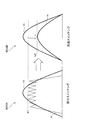
- a waveform W24A in FIG. 24 is a waveform diagram of the AC power supply voltage vs and the circuit current is in the positive half cycle in the partial switching control.
- the peak value is1 shown is the peak value of the circuit current is in the partial switching control.
- a waveform W24B is a waveform diagram of the AC power supply voltage vs and the circuit current is in the positive half cycle in the high-speed switching control.
- a peak value is2 shown in the waveform W24B is a peak value of the circuit current is in the high-speed switching control. As shown by the waveform W24B, the peak value is2 of the circuit current is in the high-speed switching control is smaller than the peak value is1 of the circuit current is in the partial switching control.
- the power factor in the high-speed switching control is higher than the power factor in the partial switching control, so that the DC voltage Vd is boosted excessively in the high-speed switching control.
- the on-duty of the switching elements Q1, Q2 is adjusted so that the peak value is1> the peak value is2. That is, when switching from one of the partial switching control and the high-speed switching control to the other, converter control unit 15d gradually changes the on-duty of switching elements Q1 and Q2 so as to suppress fluctuations in DC voltage Vd of smoothing capacitor C1. Make adjustments. Thereby, when shifting from one of the partial switching control and the high-speed switching control to the other, the fluctuation of the DC voltage Vd is suppressed, and the DC voltage Vd gradually changes.
- the converter control unit 15d switches the control mode at the zero cross timing of the AC power supply voltage vs.
- the converter control unit 15d switches from partial switching control to high-speed switching control at the zero cross timing of the AC power supply voltage vs.
- the control mode is switched, it is possible to prevent the control from becoming unstable and the DC voltage Vd from fluctuating.
- the current is actively supplied to the switching elements Q1 to Q4 by performing the synchronous rectification control at the time of low load.
- loss in the parasitic diodes D1 to D4 can be suppressed, and power conversion can be performed with high efficiency.
- partial switching control is performed at the rated load, and the switching elements Q1 and Q2 are alternately switched a predetermined number of times. Thereby, boosting, power factor improvement, and harmonic suppression can be performed. In addition, switching loss can be reduced because the number of times of switching is small compared to high-speed switching control.
- high-speed switching control is performed at high load so that the switching elements Q1 and Q2 are alternately switched at a predetermined cycle. Thereby, boosting, power factor improvement, and harmonic suppression can be performed.
- the circuit current is has a sine wave shape (see the waveform W11B in FIG. 11), and thus is particularly effective in improving the power factor and suppressing harmonics.
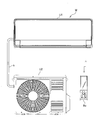
- FIG. 25 is a schematic configuration diagram of an air conditioner W according to the second embodiment.
- the air conditioner W includes an indoor unit U1, an outdoor unit U2, a pipe k that connects the two, and a remote controller Re.
- the air conditioner W is a device that performs air conditioning (cooling operation, heating operation, dehumidifying operation, etc.) by circulating a refrigerant in a known heat pump cycle.
- the remote controller Re transmits / receives predetermined various signals (operation / stop command, change of set temperature, setting of timer, change of operation mode, etc.) to and from the indoor unit U1.
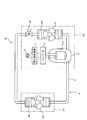
- FIG. 26 is a cooling system diagram of the air conditioner W.
- the indoor unit U1 includes an indoor heat exchanger 44 and an indoor fan F2.
- the outdoor unit U2 includes the power conversion device 1, the inverter 2, the compressor 41 incorporating the motor 41a, the outdoor heat exchanger 42, and the expansion valve 43.
- the indoor unit U1 and the outdoor unit U2 are connected via a pipe k through which a refrigerant flows, and are connected via a communication line (not shown).
- the power conversion device 1 in the outdoor unit U ⁇ b> 2 converts the AC voltage supplied from the AC power supply G into a DC voltage and supplies it to the inverter 2.
- the inverter 2 converts the DC voltage into an AC voltage having an arbitrary frequency by, for example, PWM control (Pulse Width Modulation), and drives the motor 41a to rotate.
- PWM control Pulse Width Modulation
- the compressor 41 compresses the refrigerant when the motor 41a is driven to rotate.
- the outdoor heat exchanger 42 performs heat exchange between the indoor air sent from the outdoor fan F1 and the refrigerant.
- the expansion valve 43 expands and depressurizes the refrigerant flowing from the outdoor heat exchanger 42 or the indoor heat exchanger 44.
- the indoor heat exchanger 44 performs heat exchange between the indoor air sent from the indoor fan F2 and the refrigerant.
- the compressor 41, the outdoor heat exchanger 42, the expansion valve 43, the indoor heat exchanger 44, and the pipe k are connected in a ring shape so as to circulate the refrigerant in a heat pump cycle. Therefore, these are collectively referred to as “refrigerant circuit 4”.
- the air conditioner W may be for cooling or for heating. Moreover, you may provide the four-way valve (not shown) which switches the direction through which a refrigerant
- the control unit 15 includes the circuit current Is (effective value) detected by the current detection unit 11 (see FIG. 1), and predetermined threshold values I1 (first threshold value) and I2 (second threshold value). Is different from the first embodiment in that the control mode of the power converter 1 is switched according to the result. A process for switching the control mode will be described.
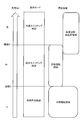
- FIG. 27 is a diagram illustrating a relationship between the magnitude of the load, the control mode, and the operation region of the device in the second embodiment.
- a region where the circuit current Is is less than the threshold value I1 is a region where the magnitude of the load (that is, the circuit current Is which is an effective value) is relatively small.
- the control unit 15 selects “synchronous rectification control” as the control mode so as to achieve high efficiency.
- the region where the circuit current Is is greater than or equal to the threshold value I1 and less than the threshold value I2 has a larger load than the intermediate operation region, and is a region where the motor 41a of the compressor 41 (that is, the load H shown in FIG. 1) can be rated. It is. In the air conditioner W, this region is referred to as a “rated operation region”. In this region, the control unit 15 selects “partial switching control” as the control mode, and realizes boosting, power factor improvement, and suppression of harmonic current.
- the region where the circuit current Is is equal to or greater than the threshold value I2 is a region where the load is relatively large.
- the operation region corresponds to the case where the heating operation is performed when the outside air temperature is very low, or the case where the cooling operation is performed when the outside air temperature is very high.
- this region is referred to as a “low temperature heating / high load region”.
- a part of “low temperature heating / high load region” overlaps with “rated operation region”.
- the control unit 15 selects “high-speed switching control” as the control mode, selects “synchronous rectification control”, and performs step-up, power factor improvement, and harmonic suppression. I am doing so.
- the magnitudes of the threshold values I1 and I2 described above may be set as appropriate based on prior experiments and simulations.
- FIG. 28 is a flowchart of a control program executed by the control unit 15 of the power conversion device 1. It is assumed that the motor 41a (see FIG. 26) is driven at the time of “START” in FIG.
- the control unit 15 reads the circuit current Is (effective value) detected by the current detection unit 11.
- the control unit 15 determines whether or not the circuit current Is read in step S101 is less than a threshold value I1 (first threshold value). That is, the control unit 15 determines whether or not the circuit current Is is included in the “intermediate operation region” (see FIG. 27).
- a threshold value I1 first threshold value
- step S102 When the circuit current Is is less than the threshold value I1 (S102: Yes), the process of the control unit 15 proceeds to step S103, and the control unit 15 executes synchronous rectification control.
- the control unit 15 executes synchronous rectification control.
- step S104 the control unit 15 determines whether or not the circuit current Is is less than the threshold value I2 (second threshold value). That is, the control unit 15 determines whether or not the circuit current Is is included in the “rated operation region” (see FIG. 27). As described above, the threshold value I2 is larger than the threshold value I1.
- step S105 the control unit 15 performs partial switching control. As described above, by performing the partial switching control in the rated operation region, it is possible to perform boosting, power factor improvement, and harmonic suppression as described in the first embodiment.
- step S104 the process of the control unit 15 proceeds to step S106.
- step S106 the control unit 15 executes high-speed switching control. As a result, even if a large circuit current is flows in the high load operation region, the power factor can be improved and harmonics can be suppressed.
- the process of the control unit 15 returns to “START” (RETURN).
- the diode rectification control see FIGS. 3 and 4) described in the first embodiment may be performed.
- the present invention is not limited to the above-described embodiments, and various modifications can be made.
- the above-described embodiments are illustrated for easy understanding of the present invention, and are not necessarily limited to those having all the configurations described.
- a part of the configuration of an embodiment can be replaced with the configuration of another embodiment, and the configuration of another embodiment can be added to the configuration of an embodiment.
- the control lines and information lines shown in the figure are those that are considered necessary for the explanation, and not all the control lines and information lines that are necessary on the product are shown. Actually, it may be considered that almost all the components are connected to each other. Examples of possible modifications to the above embodiment are as follows.
- FIG. 29 is a block diagram of a power converter 1A according to the first modification.
- a power conversion device 1A shown in FIG. 29 has a configuration in which a reactor L2 is added between the current detection unit 11 and the AC power supply G in the power conversion device 1 (see FIG. 1) of the first embodiment.
- Reactor L2 is provided on wiring hb that connects connection point N2 and AC power supply G.
- FIG. 30 is a block diagram of a power conversion device 1B according to a second modification.
- the power conversion device 1B shown in FIG. 30 uses IGBTs (Insulated-Gate-Bipolar-Transistors) instead of MOSFETs as the switching elements Q1, Q2 connected to the reactor L1 via the connection point N1. This is different from the first embodiment (see FIG. 1). As described above, even when the IGBT is used as the switching elements Q1 and Q2, the same effect as that of the first embodiment is obtained.
- IGBTs Insulated-Gate-Bipolar-Transistors
- FRD Flust-Recovery-Diode
- SiC-SBD Silicon-Carbide-Schokky Barrier-Diodes
- a super junction MOSFET having a low on-resistance may be used as the switching elements Q1 to Q4.
- SJMOSFET super junction MOSFET
- trr time during which the reverse recovery current flows
- reverse recovery current is the moment when the voltage applied to the parasitic diodes D1 to D4 is switched from the forward voltage to the reverse voltage. It is a flowing current.
- SJMOSFET having a reverse recovery time of 300 nsec or less as switching elements Q1 to Q4
- loss can be reduced and further efficiency can be improved.
- switching elements Q1 to Q4 having an on-resistance of 0.2 ⁇ or less. This can reduce conduction loss in switching elements Q1-Q4.
- the reverse recovery time of the switching elements Q1, Q2 is preferably shorter than that of the switching elements Q3, Q4.
- the switching elements Q1 and Q2 are turned on / off a predetermined number of times every half cycle of the AC power supply voltage vs. Therefore, by using switching elements Q1 and Q2 having a short reverse recovery time, the reverse recovery current is reduced, so that the switching loss can be reduced.
- reverse recovery current does not occur during the power factor correction operation, and therefore, the reverse recovery time is relatively long and the on-resistance is relatively small with respect to switching elements Q1 and Q2. Also good.
- switching elements Q1 to Q4 for example, SiC (Silicon Carbide) -MOSFET or gallium nitride (GaN) element may be used. Thereby, the energy loss of the power converter device 1 can be further reduced, and high efficiency can be achieved.
- SiC Silicon Carbide
- GaN gallium nitride
- FIG. 31 is a block diagram of a power conversion device 1C according to a third modification.
- a power conversion device 1C illustrated in FIG. 31 has a configuration in which a current sensor CT is newly added to the wiring ha in the power conversion device 1 according to the first embodiment illustrated in FIG.
- a current transformer or a Hall element may be used for the current sensor CT.
- the synchronous rectification control of the switching elements Q3 and Q4 is performed using the current value detected by the shunt resistor R1 so that no backflow current is generated.
- the current since the current during the power factor correction operation cannot be detected, the current is detected when the power factor correction operation is off. Therefore, as described above, in order to prevent the backflow of the current to the AC power supply side, the current is detected by the shunt resistor, and the state where the circuit current is surely detected is detected, and then the synchronous live flow of the switching element Q3 or Q4 Was moving. Therefore, synchronous rectification is not performed for the first shot.
- FIG. 32 shows AC power supply voltage vs, circuit current is, power factor correction current isp, shunt current ish, and drive pulses of switching elements Q1 to Q4 when partial switching control (two shots) is performed in the circuit configuration of FIG.
- FIG. 6 is a waveform diagram showing temporal changes (waveforms W32A to W32G).
- FIG. 33 is a block diagram of a control system and the like of the power conversion device according to the fourth modification.
- transistors Tr1 and Tr2 are applied instead of the diodes D5 and D6 which are transfer elements.
- the transistors Tr1 and Tr2 are turned on when the output voltage waveform “Fault” output from the drive circuit IC1 becomes 0V, and a voltage of 0V is applied to the HIN terminal and the LIN terminal of the drive circuit IC2.
- other switching elements such as IGBTs and MOSFETs may be applied. Even in such a configuration, it is possible to quickly protect each part against a short-circuit current generated in the smoothing capacitor C1.
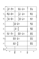
- FIG. 34 is an explanatory diagram regarding switching of the control mode of the power conversion device according to other various modifications.
- Control methods X1 to X8 in the figure show control mode selection methods in other various modifications.
- the hardware configuration of the power conversion device in these modified examples is the same as that of the first and second embodiments.
- synchronous rectification means that “synchronous rectification control” is selected as the control mode.
- synchronous rectification + partial SW means that the partial switching control includes the above-described synchronous rectification control (that is, the power factor correction operation and the synchronous rectification control are alternately performed).
- Synchronous rectification + high-speed SW means that high-speed switching control includes synchronous rectification control.
- diode rectification + partial SW means that diode rectification control is included in the partial switching control.
- the “diode rectification control” is an operation of flowing the circuit current is through the parasitic diode D1 and the like. That is, “diode rectification + partial SW” means that partial switching control is performed by alternately performing power factor correction operation and diode rectification control.
- “Diode rectification + high-speed SW” means that diode rectification control is included in high-speed switching control.
- control method X1 when the load (for example, the circuit current Is detected by the current detection unit 11) is equal to or greater than the threshold value I1, partial switching control including synchronous rectification control is performed, and the load is set to the threshold value I1. If it is less, synchronous rectification control may be performed.
- the control method X2 when the load is equal to or higher than the threshold value I1, high-speed switching control including synchronous rectification control is performed, and when the load is less than the threshold value I1, synchronous rectification control is performed. You may do it.
- the control method X3 shown in FIG. 34 is the same as the control method described in the second embodiment (see FIGS. 27 and 28). Further, for example, as shown in the control method X4, when the load is greater than or equal to the threshold value I1, partial switching control including diode rectification control is performed, and when the load is less than the threshold value I1, synchronous rectification control is performed. You may do it. By performing diode rectification control in this way, only one switching element is required to be turned on in a half cycle of the AC power supply voltage vs. Therefore, control can be simplified.
- control method X5 to X8 shown in FIG. 34 is omitted, but the control method may be appropriately set in consideration of efficiency, suppression of harmonics, boosting, and the like. For example, if the main objectives are high efficiency, suppression of harmonic current, and boosting, any one of the control methods X1 to X3 may be selected. Further, when the main purpose is not to increase the efficiency but to suppress and boost the harmonic current, the control methods X4 to X6 may be selected.
- the current value of the inverter 2 (see FIG. 26) connected to the output side of the smoothing capacitor C1 (see FIG. 1), the rotation speed of the motor 41a (see FIG. 26) connected to the inverter 2, and the motor voltage
- the control mode may be switched based on a modulation rate that is a ratio with the voltage applied to the inverter.
- the current (rotational speed and modulation factor of the motor 41a) flowing through the inverter 2 also increases. Therefore, the relationship between the load region divided by a plurality of threshold values and the current flowing through the inverter 2 (the rotational speed and modulation factor of the motor 41a) is the same as that in FIG.
- each embodiment demonstrated the structure which detects the circuit current is by shunt resistor R1 (refer FIG. 1), it is not restricted to this.
- a high-speed current transformer may be used instead of the shunt resistor R1.
- a rectifier diode (not shown) may be connected in antiparallel to each of the switching elements Q1 to Q4.
- each embodiment demonstrated the structure which the power converter device 1 is a 2 level converter it is applicable also to a 3 level or 5 level converter, for example.
- the motor 41a of the compressor 41 (see FIG. 26) described in the second embodiment may be driven by performing power conversion using any one of the control methods X1 to X8 (see FIG. 34). Good.
- the apparatus which can apply the power converter device 1 is not restricted to this.
- the power conversion device 1 may be mounted on a vehicle such as a train or an automobile, a refrigerator, a water heater, a washing machine, a vehicle such as a ship or an aircraft, or a charging facility for a battery.
- each of the above-described configurations, functions, processing units, processing means, etc. may be partially or entirely realized by hardware such as an integrated circuit.
- Each of the above-described configurations, functions, and the like may be realized by software by the processor interpreting and executing a program that realizes each function.
- Information such as programs, tables, and files for realizing each function may be recorded on a recording device such as a memory or a hard disk, or a recording medium such as a flash memory card or a DVD (Digital Versatile Disk).
Landscapes
- Engineering & Computer Science (AREA)
- Physics & Mathematics (AREA)
- Thermal Sciences (AREA)
- Chemical & Material Sciences (AREA)
- Combustion & Propulsion (AREA)
- Mechanical Engineering (AREA)
- General Engineering & Computer Science (AREA)
- Power Engineering (AREA)
- Rectifiers (AREA)
- Air Conditioning Control Device (AREA)
- Inverter Devices (AREA)
Abstract
安価でありながら素子の破壊を防止できる電力変換装置を提供する。そのため、第1および第2スイッチング素子(Q1,Q2)を駆動するとともに、ブリッジ回路に流れる電流における過電流の有無を検出し、過電流を検出した場合に所定の電圧信号(0V)を出力する出力端子(Fault端子)を有する第1の駆動回路(IC1)と、第3および第4スイッチング素子(Q3,Q4)を駆動する第2の駆動回路(IC2)と、第1の駆動回路(IC1)の出力端子(Fault端子)と、第2の駆動回路(IC2)の入力端子(LIN,HIN)との間に接続され、電圧信号(0V)を入力端子(LIN,HIN)に伝達する伝達素子(D5,D6)と、を設けた。
Description
本発明は、電力変換装置および空気調和機に関する。
電車、自動車、空気調和機等には、交流電圧を直流電圧に変換する電力変換装置(直流電源装置、コンバータ)が搭載されている。そして、電力変換装置から出力される直流電圧をインバータによって所定周波数の交流電圧に変換し、この交流電圧をモータ等の負荷に印加するようになっている。このような電力変換装置において、高調波電流規制に準拠して高調波を抑制し、また、電力変換効率を高めて省エネルギ化を図ることが求められている。
例えば、下記特許文献1の要約書には、「コンバータ回路(2)のブリッジ回路(2a)の2つのダイオード(D1,D2)には、SiC素子を用いたMOS-FETのスイッチング素子(T1,T2)が並列接続されている。そして、スイッチング素子(T1,T2)に商用電源(5)の逆電圧が作用するタイミングで該スイッチング素子(T1,T2)がオンされる。これにより、確実に同期整流が行われる」と記載されている。
例えば、下記特許文献1の要約書には、「コンバータ回路(2)のブリッジ回路(2a)の2つのダイオード(D1,D2)には、SiC素子を用いたMOS-FETのスイッチング素子(T1,T2)が並列接続されている。そして、スイッチング素子(T1,T2)に商用電源(5)の逆電圧が作用するタイミングで該スイッチング素子(T1,T2)がオンされる。これにより、確実に同期整流が行われる」と記載されている。
ところで、特許文献1のようにダイオードによる整流回路ではなく、スイッチング素子を回路に含んだ回路構成においては、過電流や短絡電流による素子の破壊を確実に防ぐため保護制御を行うことが好ましい。しかし、保護制御を行うことはコストアップにつながる。
この発明は上述した事情に鑑みてなされたものであり、安価でありながら素子の破壊を防止できる電力変換装置および空気調和機を提供することを目的とする。
この発明は上述した事情に鑑みてなされたものであり、安価でありながら素子の破壊を防止できる電力変換装置および空気調和機を提供することを目的とする。
上記課題を解決するため本発明の電力変換装置にあっては、第1スイッチング素子と、前記第1スイッチング素子に直列に接続され前記第1スイッチング素子とともに第1レグを構成する第2スイッチング素子と、第3スイッチング素子と、前記第3スイッチング素子に直列に接続され前記第3スイッチング素子とともに第2レグを構成する第4スイッチング素子と、を有し、前記第1レグと前記第2レグとを並列接続したブリッジ回路と、交流電源と前記第1レグ間に設けられたリアクトルと、前記ブリッジ回路に接続され、前記ブリッジ回路から印加される電圧を平滑化し、直流電圧として出力する平滑コンデンサと、前記第1ないし第4スイッチング素子を制御する制御部と、前記平滑コンデンサの負極と前記第2スイッチング素子との間に設けられた電流センサと、前記第1および第2スイッチング素子を駆動するとともに、前記ブリッジ回路に流れる電流における過電流の有無を検出し、前記過電流を検出した場合に所定の電圧信号を出力する出力端子を有する第1の駆動回路と、前記第3および第4スイッチング素子を駆動する第2の駆動回路と、前記第1の駆動回路の前記出力端子と、前記第2の駆動回路の入力端子との間に接続され、前記電圧信号を前記入力端子に伝達する伝達素子と、を有することを特徴とする。
本発明によれば、安価でありながら素子の破壊を防止できる。
[第1実施形態]
<電力変換装置の構成>
図1は、第1実施形態による電力変換装置1の全体ブロック図である。
電力変換装置1は、交流電源Gから印加される交流電源電圧Vsを直流電圧Vdに変換し、この直流電圧Vdを負荷H(インバータ、モータ等)に出力するコンバータである。電力変換装置1は、その入力側が交流電源Gに接続され、出力側が負荷Hに接続されている。
<電力変換装置の構成>
図1は、第1実施形態による電力変換装置1の全体ブロック図である。
電力変換装置1は、交流電源Gから印加される交流電源電圧Vsを直流電圧Vdに変換し、この直流電圧Vdを負荷H(インバータ、モータ等)に出力するコンバータである。電力変換装置1は、その入力側が交流電源Gに接続され、出力側が負荷Hに接続されている。
図1に示すように、電力変換装置1は、ブリッジ回路10と、リアクトルL1と、平滑コンデンサC1と、電流検出部11と、交流電圧検出部12と、直流電圧検出部13と、負荷検出部14と、シャント抵抗器R1と、制御部15と、を備えている。
ブリッジ回路10は、スイッチング素子Q1(第1スイッチング素子)と、スイッチング素子Q2(第2スイッチング素子)と、スイッチング素子Q3(第3スイッチング素子)と、スイッチング素子Q4(第4スイッチング素子)と、を備えている。
ブリッジ回路10は、その入力側が交流電源Gに接続され、出力側が負荷Hに接続されている。また、ブリッジ回路10のスイッチング素子Q1~Q4は、図1に示すように、ブリッジ形に接続されている。
ブリッジ回路10は、その入力側が交流電源Gに接続され、出力側が負荷Hに接続されている。また、ブリッジ回路10のスイッチング素子Q1~Q4は、図1に示すように、ブリッジ形に接続されている。
スイッチング素子Q1~Q4は、例えば、MOSFET(Metal-Oxide-Semiconductor Field-Effect Transistor)であり、制御部15によってオン/オフが制御される。なお、スイッチング素子Q1~Q4としてMOSFETを用いることで、スイッチング損失を低減できるとともに、スイッチングを高速で行えるという利点がある。
また、スイッチング素子Q1は、その内部に寄生ダイオードD1を有している。寄生ダイオードD1は、スイッチング素子Q1のソースとドレインとの間に存在するpn接合の部分である。
また、スイッチング素子Q1は、その内部に寄生ダイオードD1を有している。寄生ダイオードD1は、スイッチング素子Q1のソースとドレインとの間に存在するpn接合の部分である。
なお、スイッチング素子Q1の飽和電圧(オン状態におけるドレイン・ソース間電圧)は、寄生ダイオードD1の順方向の電圧降下よりも低いことが好ましい。これによって、寄生ダイオードD1に電流を流すよりも、スイッチング素子Q1のソース・ドレインに電流を流すほうが電圧降下は小さくなり、ひいては、導通損失を低減できるからである。換言すると、オフ状態のスイッチング素子Q1において寄生ダイオードD1に電流を流すよりも、オン状態のスイッチング素子Q1に電流を流すほうが導通損失は小さくなるようにしている。なお、他のスイッチング素子Q2~Q4についても同様のことがいえる。
本実施形態で使用しているスイッチング素子Q1とスイッチング素子Q2の寄生ダイオードの逆回復時間(trr)は、スイッチング素子Q3とスイッチング素子Q4の寄生ダイオードの逆回復時間よりも相対的に小さい。これは、スイッチング素子Q1とスイッチング素子Q2は後述する力率改善動作時に寄生ダイオードに逆回復電流が発生してしまうため、スイッチング素子Q1とQ2はスイッチング素子Q3とQ4に対して相対的に寄生ダイオードの逆回復時間の小さい素子を使用することでスイッチング損失を低減するためである。
図1に示すように、ブリッジ回路10は、スイッチング素子Q1,Q2が直列接続されてなる第1レグJ1と、スイッチング素子Q3,Q4が直列接続されてなる第2レグJ2と、が並列接続された構成になっている。
第1レグJ1において、スイッチング素子Q1のソースと、スイッチング素子Q2のドレインと、が接続され、その接続点N1は、配線haを介して交流電源Gに接続されている。なお、配線haは、その一端が交流電源Gに接続され、他端が前述した接続点N1に接続されている。
第1レグJ1において、スイッチング素子Q1のソースと、スイッチング素子Q2のドレインと、が接続され、その接続点N1は、配線haを介して交流電源Gに接続されている。なお、配線haは、その一端が交流電源Gに接続され、他端が前述した接続点N1に接続されている。
第2レグJ2において、スイッチング素子Q3のソースと、スイッチング素子Q4のドレインとが接続され、その接続点N2は、配線hbを介して交流電源Gに接続されている。なお、配線hbは、その一端が交流電源Gに接続され、他端が前述した接続点N2に接続されている。
スイッチング素子Q1のドレインと、スイッチング素子Q3のドレインと、は互いに接続され、その接続点N3は、配線hcを介して負荷Hに接続されている。なお、配線hcは、その一端が負荷Hに接続され、他端が前述した接続点N3に接続されている。
スイッチング素子Q2のソースと、スイッチング素子Q4のソースと、は互いに接続され、その接続点N4は、配線hdを介して負荷Hに接続されている。なお、配線hdは、その一端がスイッチング素子Q2,Q4のソースに接続され、他端が負荷Hに接続されている。
スイッチング素子Q2のソースと、スイッチング素子Q4のソースと、は互いに接続され、その接続点N4は、配線hdを介して負荷Hに接続されている。なお、配線hdは、その一端がスイッチング素子Q2,Q4のソースに接続され、他端が負荷Hに接続されている。
リアクトルL1は、交流電源Gから供給される電力をエネルギとして蓄え、このエネルギを放出することで昇圧や力率の改善を行うものである。リアクトルL1は、交流電源Gとブリッジ回路10とを接続する配線haに設けられている。
平滑コンデンサC1は、ブリッジ回路10から印加される電圧を平滑化して直流電圧にするものであり、配線hc,hdを介してブリッジ回路10の出力側に接続されている。また、平滑コンデンサC1は、その正極が配線hcを介してスイッチング素子Q1,Q3のドレインに接続され、負極が配線hdを介してスイッチング素子Q2,Q4のソースに接続されている。
平滑コンデンサC1は、ブリッジ回路10から印加される電圧を平滑化して直流電圧にするものであり、配線hc,hdを介してブリッジ回路10の出力側に接続されている。また、平滑コンデンサC1は、その正極が配線hcを介してスイッチング素子Q1,Q3のドレインに接続され、負極が配線hdを介してスイッチング素子Q2,Q4のソースに接続されている。
電流検出部11は、ブリッジ回路10に流れる電流を実効値(平均電流)として検出するものであり、配線hbに設けられている。電流検出部11として、例えば、カレントトランスを用いることができる。交流電圧検出部12は、交流電源Gから印加される交流電源電圧vs(瞬時値)を検出するものであり、配線ha,hbに接続されている。
直流電圧検出部13は、平滑コンデンサC1の直流電圧Vdを検出するものであり、その正側が配線hcに接続され、負側が配線hdに接続されている。なお、直流電圧検出部13の検出値は、負荷Hに印加される電圧値が所定の目標値に達しているか否かの判定に用いられる。
直流電圧検出部13は、平滑コンデンサC1の直流電圧Vdを検出するものであり、その正側が配線hcに接続され、負側が配線hdに接続されている。なお、直流電圧検出部13の検出値は、負荷Hに印加される電圧値が所定の目標値に達しているか否かの判定に用いられる。
負荷検出部14は、負荷Hに供給される電流すなわち負荷電流を検出するものであり、この負荷Hに設置されている。負荷検出部14として、例えば、シャント抵抗器を用いることができる。なお、負荷Hがモータである場合、負荷検出部14によってモータ電流を検出し、回転速度を推定するようにしてもよい。
シャント抵抗器R1は、配線hdを介して回路を流れる電流の瞬時値(瞬時電流)を検出するものであり、この配線hdに設けられている。
シャント抵抗器R1は、配線hdを介して回路を流れる電流の瞬時値(瞬時電流)を検出するものであり、この配線hdに設けられている。
制御部15は、例えば、マイコン(Microcomputer:図示せず)であり、ROM(Read Only Memory)に記憶されたプログラムを読み出してRAM(Random Access Memory)に展開し、CPU(Central Processing Unit)が各種処理を実行するようになっている。図1において制御部15の内部は、このプログラム等によって実現される機能を示している。
すなわち、図1に示すように、制御部15は、ゼロクロス判定部15aと、昇圧比制御部15bと、ゲイン制御部15cと、コンバータ制御部15d(電流センサ)と、を備えている。制御部15は、これらによってスイッチング素子Q1~Q4のオン/オフを制御する機能を実現する。
すなわち、図1に示すように、制御部15は、ゼロクロス判定部15aと、昇圧比制御部15bと、ゲイン制御部15cと、コンバータ制御部15d(電流センサ)と、を備えている。制御部15は、これらによってスイッチング素子Q1~Q4のオン/オフを制御する機能を実現する。
ゼロクロス判定部15aは、交流電圧検出部12の検出値に基づいて、交流電源電圧vsの正負が切り替わったか否か、すなわち、ゼロクロスタイミングに達したか否かを判定する。例えば、ゼロクロス判定部15aは、交流電源電圧vsが正の期間中にはコンバータ制御部15dに‘1’の信号を出力し、交流電源電圧vsが負の期間中にはコンバータ制御部15dに‘0’の信号を出力する。
昇圧比制御部15bは、電流検出部11の検出値に基づいて、直流電圧Vdの昇圧比を設定し、その昇圧比をゲイン制御部15cおよびコンバータ制御部15dに出力する機能を有している。
ゲイン制御部15cは、電流検出部11によって検出される回路電流isの実効値と、直流電圧Vdの昇圧比と、に基づいて、電流制御ゲインを設定する機能を有している。
昇圧比制御部15bは、電流検出部11の検出値に基づいて、直流電圧Vdの昇圧比を設定し、その昇圧比をゲイン制御部15cおよびコンバータ制御部15dに出力する機能を有している。
ゲイン制御部15cは、電流検出部11によって検出される回路電流isの実効値と、直流電圧Vdの昇圧比と、に基づいて、電流制御ゲインを設定する機能を有している。
コンバータ制御部15dは、電流検出部11、直流電圧検出部13、シャント抵抗器R1、ゼロクロス判定部15a、昇圧比制御部15b、およびゲイン制御部15cから入力される情報に基づいて、スイッチング素子Q1~Q4のオン/オフを制御する。なお、コンバータ制御部15dが実行する処理については後記する。
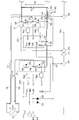
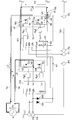
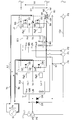
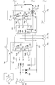
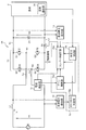
図2は、第1実施形態に係る電力変換装置1の、制御系統等のブロック図である。なお、図1に示した要素は、図2においては適宜省略している。
Rg1~Rg4はスイッチング素子Q1~Q4のゲートに接続されているゲート回路である。具体的には、ゲート回路Rg1~Rg4は、抵抗、コンデンサ、インダクタなどの受動素子やダイオード等の半導体で構成される。
Rg1~Rg4はスイッチング素子Q1~Q4のゲートに接続されているゲート回路である。具体的には、ゲート回路Rg1~Rg4は、抵抗、コンデンサ、インダクタなどの受動素子やダイオード等の半導体で構成される。
IC1,IC2はスイッチング素子Q1~Q4を駆動するための駆動回路であり、内部に集積回路を有している。駆動回路IC1,IC2は、ハイサイドの素子を駆動するために内部にレベルシフト回路を有している。駆動回路IC1(第1の駆動回路)は内部に過電流保護回路を有しているが、駆動回路IC2(第2の駆動回路)には、過電流保護回路は省略されており、その分、駆動回路IC2を安価に構成することができる。
VccはIC1とIC2の駆動電源電圧の接続端子である。HINはコンバータ制御部15dの出力ポートP1,P5に接続されており、コンバータ制御部15dから信号が入力されるとHO端子からハイサイドのスイッチング素子Q1、Q3を駆動するための駆動信号が出力される。同様にLINはコンバータ制御部15dの出力ポートP2,P6に接続されており、コンバータ制御部15dから信号が入力されるとLO端子からローサイドのスイッチング素子Q2、Q4を駆動するための駆動信号が出力される。
駆動回路IC1,IC2のVs端子は、接続点N1、N2にそれぞれ接続されている。GND端子は平滑コンデンサC1の負極側の配線hd上の接続点N5に接続されている。ITrip端子はスイッチング素子Q2、Q4のドレインと同電位である接続点N6に接続されている。Fault端子は接続点N7を介してコンバータ制御部15dの入力ポートP4に接続されている。シャント抵抗器R1はコンバータ制御部15dの入力ポートP3に接続されている。
ここで、駆動回路IC1の保護回路の動作について説明する。シャント抵抗器R1に電流が接続点N4からN5の向きに電流が流れた場合、IC1のGND端子を基準にITrip端子には電圧が発生する。このとき、シャント抵抗器R1に過電流が通流して、ITrip端子に発生する電圧が所定値を超えた場合、IC1内の駆動回路がHIN、LIN側からの入力信号を遮断することで、スイッチング素子Q1とQ2を強制的にオフさせる。それと同時に、Fault端子からコンバータ制御部15dのポートP4へ0Vを出力する。通常、この保護動作を行っていないときは、Fault端子からは電圧レベルVccの信号が出力され続けている。
D5はダイオードであり、アノードはIC2のHIN端子に接続されており、カソードは接続点N7を介してIC1のFault端子とコンバータ制御部15dのポートP4に接続されている。D6もダイオードであり、アノードはIC2のLIN端子に接続されており、カソードはダイオードD5のカソードと接続されており、接続点N7を介してIC1のFault端子とコンバータ制御部15dのポートP4に接続されている。
<電力変換装置の制御モード>
次に、負荷の大きさ(例えば、電流検出部11の検出値)に基づいて切り替えられる制御モードについて説明する。前述した制御モードには、「ダイオード整流制御」、「同期整流制御」、「部分スイッチング制御」、および「高速スイッチング制御」が含まれる。
次に、負荷の大きさ(例えば、電流検出部11の検出値)に基づいて切り替えられる制御モードについて説明する。前述した制御モードには、「ダイオード整流制御」、「同期整流制御」、「部分スイッチング制御」、および「高速スイッチング制御」が含まれる。
(1.ダイオード整流制御)
ダイオード整流制御は、4つの寄生ダイオードD1~D4を用いて全波整流を行う制御モードである。ダイオード整流制御は、例えば、負荷の大きさが比較的小さいときに実行されるが、これに限定されるものではない。
ダイオード整流制御は、4つの寄生ダイオードD1~D4を用いて全波整流を行う制御モードである。ダイオード整流制御は、例えば、負荷の大きさが比較的小さいときに実行されるが、これに限定されるものではない。
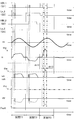
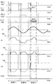
図3は、ダイオード整流制御における交流電源電圧vs、回路電流is、およびスイッチング素子Q1~Q4の駆動パルスの時間的変化を示す波形図である。
なお、波形W3Aは、交流電源電圧vs(瞬時値)の波形であり、波形W3Bは、回路電流is(瞬時値)の波形である。波形W3C,W3D,W3E,W3Fは、スイッチング素子Q1~Q4の駆動パルスの波形である。
図3の波形W3C,W3D,W3E,W3Fに示すように、コンバータ制御部15dは、スイッチング素子Q1~Q4の全てをオフ状態に維持することで、次に説明するように、寄生ダイオードD1~D4を介して回路電流isを流す。
なお、波形W3Aは、交流電源電圧vs(瞬時値)の波形であり、波形W3Bは、回路電流is(瞬時値)の波形である。波形W3C,W3D,W3E,W3Fは、スイッチング素子Q1~Q4の駆動パルスの波形である。
図3の波形W3C,W3D,W3E,W3Fに示すように、コンバータ制御部15dは、スイッチング素子Q1~Q4の全てをオフ状態に維持することで、次に説明するように、寄生ダイオードD1~D4を介して回路電流isを流す。
図4は、ダイオード整流制御において、交流電源電圧vsが正の半サイクルに含まれるときの回路電流isの流れを示す説明図である。交流電源電圧vsが正の半サイクルの期間では、図4の破線矢印で示すように、交流電源G→リアクトルL1→寄生ダイオードD1→平滑コンデンサC1→シャント抵抗器R1→寄生ダイオードD4→交流電源Gの順に回路電流isが流れる。
また、交流電源電圧vsが負の半サイクルの期間では、図示はしないが、交流電源G→寄生ダイオードD3→平滑コンデンサC1→シャント抵抗器R1→寄生ダイオードD2→リアクトルL1→交流電源Gの順に回路電流isが流れる。なお、回路電流isの波形は、図3の波形W3Bに示す通りである。
このようなダイオード整流制御を低負荷時に行うことにより、スイッチング素子Q1~Q4におけるスイッチング損失を低減できる。
このようなダイオード整流制御を低負荷時に行うことにより、スイッチング素子Q1~Q4におけるスイッチング損失を低減できる。
(2.同期整流制御)
同期整流制御は、平滑コンデンサC1を介した電流経路に含まれるスイッチング素子のうち、平滑コンデンサC1の正極に接続されているスイッチング素子を、ブリッジ回路10に電流が流れている期間の少なくとも一部でオン状態とし、上述した電流経路に含まれないスイッチング素子をオフ状態に維持する制御モードである。
同期整流制御は、平滑コンデンサC1を介した電流経路に含まれるスイッチング素子のうち、平滑コンデンサC1の正極に接続されているスイッチング素子を、ブリッジ回路10に電流が流れている期間の少なくとも一部でオン状態とし、上述した電流経路に含まれないスイッチング素子をオフ状態に維持する制御モードである。
図5は、同期整流制御において、交流電源電圧vsが正の半サイクルに含まれるときの電流の流れを示す説明図である。交流電源電圧vsが正の半サイクルの期間では、図5の破線矢印で示すように、交流電源G→リアクトルL1→スイッチング素子Q1→平滑コンデンサC1→シャント抵抗器R1→スイッチング素子Q4→交流電源Gの電流経路において回路電流isが流れる。
また、交流電源電圧vsが負の半サイクルの期間では、図示はしないが、交流電源G→スイッチング素子Q3→平滑コンデンサC1→シャント抵抗器R1→スイッチング素子Q2→リアクトルL1→交流電源Gの電流経路において回路電流isが流れる。
このように同期整流制御では、電源電圧の極性に同期させてスイッチング素子Q1~Q4をスイッチング制御することで、損失の小さいオン抵抗の部分に積極的に電流を流し、寄生ダイオードD1~D4には、ほとんど電流を流さないようにしている。これによって、スイッチング素子での導通損失を低減できるため高効率に電力変換を行うことができる。また、後記する部分スイッチング制御や高速スイッチング制御と比較して、同期整流制御では力率改善動作を行わない。従って、適度な力率を保ちながらもスイッチング損失を低減できるため、高効率で電力変換を行うことができる。
このように同期整流制御では、電源電圧の極性に同期させてスイッチング素子Q1~Q4をスイッチング制御することで、損失の小さいオン抵抗の部分に積極的に電流を流し、寄生ダイオードD1~D4には、ほとんど電流を流さないようにしている。これによって、スイッチング素子での導通損失を低減できるため高効率に電力変換を行うことができる。また、後記する部分スイッチング制御や高速スイッチング制御と比較して、同期整流制御では力率改善動作を行わない。従って、適度な力率を保ちながらもスイッチング損失を低減できるため、高効率で電力変換を行うことができる。
図6は、同期整流制御における交流電源電圧vs、回路電流is、シャント抵抗器R1に流れる電流ish、およびスイッチング素子Q1~Q4の駆動パルスの時間的変化を示す説明図である。
同期整流制御において、コンバータ制御部15dは、回路電流isに同期させて、スイッチング素子Q1~Q4のオン/オフを切り替える。交流電源電圧vsが正の半サイクルの区間を例にして説明する。交流電源電圧のゼロクロスは、交流電圧検出部12とゼロクロス判定部15aによって検出する。図6の波形W6A,W6Bに示すように、交流電源電圧のゼロクロスから一定時間経過後、回路電流Isが流れ始める。
同期整流制御において、コンバータ制御部15dは、回路電流isに同期させて、スイッチング素子Q1~Q4のオン/オフを切り替える。交流電源電圧vsが正の半サイクルの区間を例にして説明する。交流電源電圧のゼロクロスは、交流電圧検出部12とゼロクロス判定部15aによって検出する。図6の波形W6A,W6Bに示すように、交流電源電圧のゼロクロスから一定時間経過後、回路電流Isが流れ始める。
さらに詳細に波形を検討すると、回路電流isが流れ始めるのは、交流電源電圧vsが増大していき、直流電圧Vdと等しくなった後、さらに時間dt1が経過したタイミングである。そして、直流電圧Vdが交流電圧と再び等しくなった後、さらに時間dt2経過後に回路電流がゼロになる。すなわち、交流電源電圧vsに対して直流電圧Vdが大きいときに電流が流れ、反対に交流電源電圧vsに対して直流電圧Vdが大きい場合には回路電流isは流れない。但し、実際には、前述のように時間遅れdt1、dt2が発生する。これらの現象は、リアクトルL1によって時間的遅れが発生するためである。なお、時間dt2は、以下の(数式1)で表される。

交流電源電圧vsが正の極性の場合、コンバータ制御部15dは、ゼロクロスのタイミングで、まずスイッチング素子Q1のゲートに駆動パルスを入力し、スイッチング素子Q1をオン状態にする。その後、回路電流is>0となり、所定のタイミングでスイッチング素子Q4のゲートに駆動パルスを入力し、スイッチング素子Q4をオン状態にする。次に、このスイッチング素子Q4の駆動方法を説明する。
スイッチング素子Q4をオン/オフさせるタイミングは、シャント抵抗器R1で検出した電流ish(以下、シャント電流と呼ぶ)の検出値によって判定する。
コンバータ制御部15dには、二つの電流判定値すなわち判定値a(第1の判定閾値)と判定値b(第2の判定閾値)とが予め記憶されている。図6に示すように、シャント電流ishが判定値a以上となったタイミングでコンバータ制御部15dはスイッチング素子Q4に駆動パルスを入力して、スイッチング素子Q4をオン状態にする。その後、回路電流が判定値b以下になったタイミングで、コンバータ制御部15dはスイッチング素子Q4をオフさせる。
コンバータ制御部15dには、二つの電流判定値すなわち判定値a(第1の判定閾値)と判定値b(第2の判定閾値)とが予め記憶されている。図6に示すように、シャント電流ishが判定値a以上となったタイミングでコンバータ制御部15dはスイッチング素子Q4に駆動パルスを入力して、スイッチング素子Q4をオン状態にする。その後、回路電流が判定値b以下になったタイミングで、コンバータ制御部15dはスイッチング素子Q4をオフさせる。
このように、本実施形態の電力変換装置1は、同期整流を行ううえでスイッチング素子Q1とQ4をオンさせるタイミングをずらしている。すなわち、交流電源電圧vsが正の極性の場合は、スイッチング素子Q1をオンさせてから所定時間経過後にスイッチング素子Q4をオンさせている。これは、平滑コンデンサC1、すなわち直流電圧側から交流電源への電流の逆流を防ぐためである。
例えば、交流電源電圧vs<直流電圧Vdの領域でスイッチング素子Q1とQ4が共にオン状態であると、平滑コンデンサC1→スイッチング素子Q1→リアクトルL1→交流電源G→スイッチング素子Q4→平滑コンデンサC1という電流逆流のループが発生してしまう。さらに、交流電源電圧vs>直流電圧Vdかつ回路電流is=0の領域(図6における波形W6Aの時間dt1の領域)でスイッチング素子Q1とスイッチング素子Q4がオン状態になった場合も、回路電流isが通流していないため、前述の逆流ループで平滑コンデンサC1から交流電源Gへ逆流電流が発生してしまう。そのため、本実施形態ではスイッチング素子Q1とスイッチング素子Q4が共にオン状態にするのは、交流電源電圧vs>直流電圧Vdかつ回路電流is>0の領域としている。
さらに詳細に説明すると、本実施形態の電力変換装置1では、交流電源電圧のゼロクロス検出後、まずQ1をオンさせ、交流電圧vs>直流電圧Vdかつis>0となり、特定のタイミング(シャント電流ishまたは回路電流isが前述の判定値a以上となったとき)でQ4をオンさせている。すなわち、交流電源電圧vsが正の極性の領域においては、スイッチング素子Q4→Q1の順でオンさせて同期整流を行っている。
前述のようにスイッチング素子Q1とQ4のスイッチングのタイミングを誤ると回路に逆流電流が発生してしまう。これを防ぐためにスイッチング素子Q1とQ4をオンさせるタイミングをずらすが、ここでスイッチング素子Q1とQ4の何れを先にオンさせるかが問題となる。
前述のようにスイッチング素子Q1とQ4のスイッチングのタイミングを誤ると回路に逆流電流が発生してしまう。これを防ぐためにスイッチング素子Q1とQ4をオンさせるタイミングをずらすが、ここでスイッチング素子Q1とQ4の何れを先にオンさせるかが問題となる。
図7を参照して、その問題を説明する。なお、図7は、スイッチング素子Q1とQ4のドレイン逆電流と寄生ダイオードの飽和電圧の関係を示した特性図である。
ここで、ドレイン逆電流とは、スイッチング素子のソースからドレインの向きに流れる電流を意味している。寄生ダイオード飽和電圧とは、ドレイン逆電流が寄生ダイオードに通流した場合に寄生ダイオードで発生する電圧降下を意味している。
前述のようにスイッチング素子Q1の寄生ダイオードD1の逆回復時間はスイッチング素子Q4の寄生ダイオードD4の逆回復時間に対して相対的に小さい。そして、それぞれの寄生ダイオードの飽和電圧は図7のような関係になる。
ここで、ドレイン逆電流とは、スイッチング素子のソースからドレインの向きに流れる電流を意味している。寄生ダイオード飽和電圧とは、ドレイン逆電流が寄生ダイオードに通流した場合に寄生ダイオードで発生する電圧降下を意味している。
前述のようにスイッチング素子Q1の寄生ダイオードD1の逆回復時間はスイッチング素子Q4の寄生ダイオードD4の逆回復時間に対して相対的に小さい。そして、それぞれの寄生ダイオードの飽和電圧は図7のような関係になる。
ドレイン逆電流が「小」の領域では寄生ダイオードの飽和電圧はほとんど変わらないが、ドレイン逆電流が「中」または「大」の領域では、スイッチング素子Q4の寄生ダイオードの飽和電圧に対してスイッチング素子Q1の寄生ダイオードの飽和電圧は大きくなっている。これは、電流が大きくなるほど寄生ダイオードで発生する導通損失は、スイッチング素子Q4(寄生ダイオードD4)に対してスイッチング素子Q1(寄生ダイオードD1)の方が大きいことを意味している。なお、図7のグラフにおいて、ドレイン逆電流「小」の領域は電力変換装置1を備えた機器が通常使用しないような軽負荷の領域であり、ドレイン逆電流「中」の領域は電力変換装置1を備えた機器が通常運転動作で使用する領域であり、ドレイン逆電流「大」の領域は電力変換装置1を備えた機器が過負荷動作で使用する領域を意味している。
図6に戻り、回路電流isが流れ始めてからスイッチング素子Q4がオンするまでの時間dt3の区間では、スイッチング素子Q1はオン状態になる。これにより、スイッチング素子Q1において、回路電流isは、損失の小さいオン抵抗の部分に流れる。一方、スイッチング素子Q4はオフ状態になるため、回路電流isは寄生ダイオードD4に流れる。すなわち、時間dt3で発生する損失(面積Sの部分)は、スイッチング素子Q1のオン抵抗で発生する通流損と、スイッチング素子Q4の寄生ダイオードで発生する通流損の合計値となる。
仮に、交流電源電圧vsのゼロクロス検出後、スイッチング素子Q4を先にオン状態とし、回路電流is、シャント電流ishが判定値aに達したところでスイッチング素子Q1をオン状態にする、という順番で駆動した、場合の動作を検討する。
この場合、面積Sの領域での損失は、スイッチング素子Q4のオン抵抗の部分と、スイッチング素子Q1の寄生ダイオードでの通流損の合計である。前述したように、スイッチング素子Q1の寄生ダイオードの通流損はスイッチング素子Q4の寄生ダイオードの通流損よりも大きい。そのため、スイッチング素子Q1→Q4の順にスイッチングした場合と比較して面積Sの部分での損失が大きくなってしまう。
この場合、面積Sの領域での損失は、スイッチング素子Q4のオン抵抗の部分と、スイッチング素子Q1の寄生ダイオードでの通流損の合計である。前述したように、スイッチング素子Q1の寄生ダイオードの通流損はスイッチング素子Q4の寄生ダイオードの通流損よりも大きい。そのため、スイッチング素子Q1→Q4の順にスイッチングした場合と比較して面積Sの部分での損失が大きくなってしまう。
このような理由により、本実施形態では、同期整流制御時に発生する導通損をなるべく抑えるために、交流電源電圧vsが正の極性時には、スイッチング素子Q1→Q4の順にオンさせている。交流電源電圧が負の極性の場合においても同様に、スイッチング素子Q2→Q3の順にスイッチングすることで、同期整流制御時の導通損をなるべく抑えることができ、高効率駆動が可能となる。
交流電源電圧vsが正の半サイクルの期間であってスイッチング素子Q1,Q4が共にオン状態であれば、図5の破線矢印で示すように、交流電源G→リアクトルL1→スイッチング素子Q1→平滑コンデンサC1→シャント抵抗器R1→スイッチング素子Q4→交流電源Gの電流経路において回路電流isが流れる。このとき、スイッチング素子Q2,Q3は、オフ状態に維持される(図6の波形W6E,W6F参照)。また、前述したように、図6の面積Sの領域において、スイッチング素子Q4に関して回路電流isは寄生ダイオードD4に流れる。
また、前述のように交流電源電圧vsが負の半サイクルの期間では、スイッチング素子Q2,Q3が共にオン状態であれば、図示は省略するが、交流電源G→スイッチング素子Q3→平滑コンデンサC1→シャント抵抗器R1→スイッチング素子Q2→リアクトルL1→交流電源Gの電流経路において回路電流isが流れる。このとき、スイッチング素子Q1,Q4は、オフ状態に維持される(図6の波形W6D,W6G参照)。また、前述したように、図6の面積Sの領域において、スイッチング素子Q3に関して回路電流isは寄生ダイオードD3に流れる。
このように、本実施形態においては、スイッチング素子Q3,Q4は、スイッチング素子Q1,Q2とは特性の異なる素子を使用している。これにより、スイッチング素子Q1,Q2の寄生ダイオードの逆回復時間は、スイッチング素子Q3,Q4の寄生ダイオードの逆回復時間よりも相対的に短い。
そして、スイッチング素子Q1,Q2の寄生ダイオードの飽和電圧Vfは、スイッチング素子Q3,Q4の寄生ダイオードの飽和電圧Vfよりも相対的に高い。さらに、同期整流制御時のスイッチング素子のオンの順番として、ゼロクロス検出後にリアクトルL1に接続されている側のスイッチング素子、すなわち寄生ダイオードの飽和電圧Vfが高い素子スイッチング素子Q1,Q2を先にオン状態にし、その後シャント電流ish(若しくは回路電流is)が判定値aに到達したらリアクトルに接続されていない側のスイッチング素子、すなわち寄生ダイオードの飽和電圧が低い側のスイッチング素子Q3,Q4をオン状態にする。
そして、スイッチング素子Q1,Q2の寄生ダイオードの飽和電圧Vfは、スイッチング素子Q3,Q4の寄生ダイオードの飽和電圧Vfよりも相対的に高い。さらに、同期整流制御時のスイッチング素子のオンの順番として、ゼロクロス検出後にリアクトルL1に接続されている側のスイッチング素子、すなわち寄生ダイオードの飽和電圧Vfが高い素子スイッチング素子Q1,Q2を先にオン状態にし、その後シャント電流ish(若しくは回路電流is)が判定値aに到達したらリアクトルに接続されていない側のスイッチング素子、すなわち寄生ダイオードの飽和電圧が低い側のスイッチング素子Q3,Q4をオン状態にする。
また、本実施形態においては、同期整流制御を行うために、交流電源電圧vsが正から負に切り替わるゼロクロスタイミングでスイッチング素子Q1,Q2のオン/オフ状態を切り替えるが、その際にスイッチング素子Q1,Q2の上下短絡を防ぐために、スイッチング素子Q1,Q2の双方がオフ状態になるデッドタイムtdを設けている。
以上のように同期整流制御を行うことで、電力変換装置1を高効率に駆動することが可能となる。
以上のように同期整流制御を行うことで、電力変換装置1を高効率に駆動することが可能となる。
(3.部分スイッチング制御)
部分スイッチング制御は、スイッチング素子Q1~Q4のうち、リアクトルL1に接続されている2つのスイッチング素子Q1,Q2を交互にオン/オフさせてリアクトルL1を短絡させる動作を所定回数行う制御モードである。このような制御により、電源力率の改善による高調波電流の低減と、直流電圧の昇圧を行うことができる。
部分スイッチング制御は、スイッチング素子Q1~Q4のうち、リアクトルL1に接続されている2つのスイッチング素子Q1,Q2を交互にオン/オフさせてリアクトルL1を短絡させる動作を所定回数行う制御モードである。このような制御により、電源力率の改善による高調波電流の低減と、直流電圧の昇圧を行うことができる。
図8は、部分スイッチング制御における交流電源電圧vs、回路電流is、シャント抵抗器R1に流れる電流ish、およびスイッチング素子Q1~Q4の駆動パルスの時間的変化を示す説明図である。
なお、図8は、2ショットすなわち半周期あたり2回だけリアクトルL1を短絡させる場合の例である。
なお、図8は、2ショットすなわち半周期あたり2回だけリアクトルL1を短絡させる場合の例である。
図8の波形W8Aに示す交流電源電圧vsが正の半サイクルである期間に着目すると、コンバータ制御部15dは、スイッチング素子Q1,Q2を所定回数・所定パルス幅で交互にオン/オフする。すなわち、コンバータ制御部15dは、交流電源電圧vsの正・負が切り替わったゼロクロスタイミングの直後から、図8の波形W8D,W8Eに示すように、スイッチング素子Q1,Q2を交互にオン/オフする動作を所定回数行う。また、波形W8F,W8Gに示すように、コンバータ制御部15dは、交流電源電圧vsの極性に同期して、スイッチング素子Q3,Q4のオン/オフ状態を設定する。
以下では、部分スイッチング制御ついて、理解しやすく説明するために、部分スイッチング制御を「力率改善動作」と「同期整流動作」とに分けて説明する。
まず、「力率改善動作」とは、スイッチング素子Q1,Q2の双方を一時的にオン状態にすることで、リアクトルL1を介して力率改善電流isp(図8の波形W8Bを参照)を流す動作である。
また、「同期整流動作」とは、交流電源電圧vsの極性に基づいてスイッチング素子Q1~Q4を制御し、平滑コンデンサC1を介して回路電流isを流す動作である。なお、上述した同期整流制御(図5、図6参照)は、この「同期整流動作」を継続的に行う制御モードである。
まず、「力率改善動作」とは、スイッチング素子Q1,Q2の双方を一時的にオン状態にすることで、リアクトルL1を介して力率改善電流isp(図8の波形W8Bを参照)を流す動作である。
また、「同期整流動作」とは、交流電源電圧vsの極性に基づいてスイッチング素子Q1~Q4を制御し、平滑コンデンサC1を介して回路電流isを流す動作である。なお、上述した同期整流制御(図5、図6参照)は、この「同期整流動作」を継続的に行う制御モードである。
詳細については後記するが、部分スイッチング制御では、上述した「同期整流動作」と「力率改善動作」とが交互に所定回数行われる。
まず、「力率改善動作」について説明する。
例えば、交流電源電圧vsが正の半サイクルの期間においてコンバータ制御部15dは、スイッチング素子Q3をオフ状態に維持するとともに(図8の波形W8Fを参照)、スイッチング素子Q4をオン状態に維持する(図8の波形W8Gを参照)。
また、コンバータ制御部15dは、交流電源電圧vsのゼロクロス後から一定時間tdelの経過後、スイッチング素子Q2をオンにするとともに(図8の波形W8Eを参照)、スイッチング素子Q1をオフにする(図8の波形W8Dを参照)。このときに流れる力率改善電流ispの経路について、図9を参照して説明する。
まず、「力率改善動作」について説明する。
例えば、交流電源電圧vsが正の半サイクルの期間においてコンバータ制御部15dは、スイッチング素子Q3をオフ状態に維持するとともに(図8の波形W8Fを参照)、スイッチング素子Q4をオン状態に維持する(図8の波形W8Gを参照)。
また、コンバータ制御部15dは、交流電源電圧vsのゼロクロス後から一定時間tdelの経過後、スイッチング素子Q2をオンにするとともに(図8の波形W8Eを参照)、スイッチング素子Q1をオフにする(図8の波形W8Dを参照)。このときに流れる力率改善電流ispの経路について、図9を参照して説明する。
図9は交流電源電圧vsが正の極性の半サイクルにおいて、力率改善動作を行ったときの電流の流れを示す説明図である。
交流電源電圧vsが正の極性のときに力率改善動作を行うと、図9の破線矢印で示すように、交流電源G→リアクトルL1→スイッチング素子Q2→スイッチング素子Q4→交流電源G、の短絡経路において、力率改善電流ispが流れる。なお、スイッチング素子Q4は後述する同期生流動作時を想定した場合であるため、短絡電流ispは寄生ダイオードD4ではなく、オン抵抗の部分に通流している。このときリアクトルL1には、以下の(数式2)で表されるエネルギが蓄えられる。なお、(数式2)に示すIspは、短絡電流ispの実効値である。
交流電源電圧vsが正の極性のときに力率改善動作を行うと、図9の破線矢印で示すように、交流電源G→リアクトルL1→スイッチング素子Q2→スイッチング素子Q4→交流電源G、の短絡経路において、力率改善電流ispが流れる。なお、スイッチング素子Q4は後述する同期生流動作時を想定した場合であるため、短絡電流ispは寄生ダイオードD4ではなく、オン抵抗の部分に通流している。このときリアクトルL1には、以下の(数式2)で表されるエネルギが蓄えられる。なお、(数式2)に示すIspは、短絡電流ispの実効値である。

従って、電力変換装置1の力率を改善できるとともに、高調波電流を抑制できる。さらに、後述するようにオンしたスイッチング素子Q2をオフにしたタイミングで、数式2で表されたリアクトルL1に蓄えられたエネルギが平滑コンデンサC1にチャージされることで直流電圧Vdが昇圧される。
なお、交流電源電圧vsが負の極性である期間では、図示は省略するが、交流電源G→スイッチング素子Q3→スイッチング素子Q1→リアクトルL1→交流電源Gの短絡経路において、短絡電流isp(力率改善電流)が流れる。
なお、交流電源電圧vsが負の極性である期間では、図示は省略するが、交流電源G→スイッチング素子Q3→スイッチング素子Q1→リアクトルL1→交流電源Gの短絡経路において、短絡電流isp(力率改善電流)が流れる。
次に、「同期整流動作」について説明する。
図8の波形W8Eに示すように、スイッチング素子Q2によって「力率改善動作」を行った後、コンバータ制御部15dは「同期整流動作」を行う。すなわち、コンバータ制御部15dは、スイッチング素子Q1をオフからオンに切り替えるとともに(図8の波形W8Dを参照)、スイッチング素子Q2をオンからオフに切り替える(図8の波形W8Eを参照)。なお、この区間、スイッチング素子Q3はオフ状態に維持される(図8の波形W8Fを参照)。
図8の波形W8Eに示すように、スイッチング素子Q2によって「力率改善動作」を行った後、コンバータ制御部15dは「同期整流動作」を行う。すなわち、コンバータ制御部15dは、スイッチング素子Q1をオフからオンに切り替えるとともに(図8の波形W8Dを参照)、スイッチング素子Q2をオンからオフに切り替える(図8の波形W8Eを参照)。なお、この区間、スイッチング素子Q3はオフ状態に維持される(図8の波形W8Fを参照)。
このように、スイッチング素子Q1とQ2のオン/オフ状態を相互に切り替えている理由は、力率改善動作と動機整流動作を切り替えているためである。例えば交流電源電圧vsが正の極性の場合、スイッチング素子Q1もスイッチング素子Q3と同様に常時オフ状態でスイッチング素子Q2のみオン/オフを行ったとすると、スイッチング素子オフ時には回路電流isはスイッチング素子Q1の寄生ダイオードD1を流れるため、高効率動作ができない。そのため、スイッチング素子Q2がオフのときはスイッチング素子Q1をオン状態にすることで同期整流動作を行い、高効率動作を行う。
さらに、本実施形態では同期整流動作による効果を高めるために、部分スイッチング制御においてもリアクトルL1に接続されていない側のスイッチング素子Q3またはQ4をスイッチング制御している。
例えば交流電源電圧vsが正の極性の場合を例に説明する。この場合、前述のようにスイッチング素子Q3は常時オフ状態である。交流電源電圧のゼロクロス後、所定時間tdelが経過した後にスイッチング素子Q2がオンとなって力率改善動作を行い、力率改善電流が回路に通流する。その後、スイッチング素子Q4は上述した同期整流制御の場合と同様に、シャント電流ishの検出が判定値aを超えたタイミングでオン状態となり、その後判定値bを下回ったタイミングでスイッチング素子Q4はオフ状態となる。
このようにスイッチング素子Q4を制御することで、前述の同期整流動作の場合と同様に、部分スイッチング制御においても、スイッチング素子Q1とスイッチング素子Q4を用いて同期整流動作を行うため、高効率動作が可能である。
例えば交流電源電圧vsが正の極性の場合を例に説明する。この場合、前述のようにスイッチング素子Q3は常時オフ状態である。交流電源電圧のゼロクロス後、所定時間tdelが経過した後にスイッチング素子Q2がオンとなって力率改善動作を行い、力率改善電流が回路に通流する。その後、スイッチング素子Q4は上述した同期整流制御の場合と同様に、シャント電流ishの検出が判定値aを超えたタイミングでオン状態となり、その後判定値bを下回ったタイミングでスイッチング素子Q4はオフ状態となる。
このようにスイッチング素子Q4を制御することで、前述の同期整流動作の場合と同様に、部分スイッチング制御においても、スイッチング素子Q1とスイッチング素子Q4を用いて同期整流動作を行うため、高効率動作が可能である。
さらに、図8は2ショットの場合(力率改善動作を2回行った場合)を説明した図であるが、3ショット(力率改善動作を3回行う)、4ショット(力率改善動作4回行う)等、力率改善動作の回数を増やしてもよい。この場合、図8の波形W8Gに示すように2ショット目以降については、スイッチング素子Q4はオン状態を維持しているため、スイッチング素子Q2による力率改善動作中も、短絡電流ispは図9に示すようにスイッチング素子Q4の寄生ダイオードD4ではなく、オン抵抗の部分に流れるため、高効率動作が可能である。そして、「力率改善動作」と「同期整流動作」とを所定回数、交互に行った後、コンバータ制御部15dは、回路電流isが流れている区間において、スイッチング素子Q1とQ4をオン状態にしているため、スイッチング素子Q1とQ4の導通損失を低減できるため、高効率動作が可能である。
本実施形態では、シャント電流ish(若しくは回路電流is)として検出した電流値に応じてスイッチング素子Q4を用いて力率改善動作と同期整流動作を行うことで電力変換装置を高効率駆動している。換言すると、前述の同期整流制御も同様であるが、力率改善動作を行っていないとき(コンバータ動作オフのとき)は回路電流isがシャント抵抗器R1に流れる。すなわち、シャント抵抗器にて電流検出(シャント電流ishの検出)が可能となる。このようにコンバータオフ時に電流検出を行い、同期整流制御、同期整流動作を行うことで高効率駆動が可能となる。
なお、力率改善動作を行うためにスイッチング素子Q1,Q2のオン/オフを切り替える際には、所定のデッドタイムを設けている。これによってスイッチング素子Q1とQ2の上下短絡を防ぐことができる。
このようにスイッチング素子Q1~Q4が制御されることで、リアクトルL1に蓄えられたエネルギが平滑コンデンサC1に放出され、平滑コンデンサC1の直流電圧が昇圧される。なお、同期整流動作における電流経路は、上述した同期整流モードにおける電流経路(図5の破線矢印を参照)と同様である。
このようにスイッチング素子Q1~Q4が制御されることで、リアクトルL1に蓄えられたエネルギが平滑コンデンサC1に放出され、平滑コンデンサC1の直流電圧が昇圧される。なお、同期整流動作における電流経路は、上述した同期整流モードにおける電流経路(図5の破線矢印を参照)と同様である。
例えば、負荷Hがモータである場合、回転速度の上昇に伴ってモータの誘起電圧が高くなり、モータが駆動しにくくなることがある。これに対して、上述した「力率改善動作」および「同期整流動作」を交互に行って昇圧することにより、モータの回転速度の許容限度を高めることができる。
なお、図8の波形W8Gに示すように、スイッチング素子Q4を所定のタイミングで制御している理由は、同期整流による高効率動作を行う他、前述した平滑コンデンサC1から交流電源へ逆流電流が流れることを防止するためでもある。なお、スイッチング素子Q1,Q2を交互にオン/オフする際のタイミングや回数は、適宜設定できる。
なお、図8の波形W8Gに示すように、スイッチング素子Q4を所定のタイミングで制御している理由は、同期整流による高効率動作を行う他、前述した平滑コンデンサC1から交流電源へ逆流電流が流れることを防止するためでもある。なお、スイッチング素子Q1,Q2を交互にオン/オフする際のタイミングや回数は、適宜設定できる。
以上、交流電源電圧vsが正の極性の場合を例に挙げて説明したが、交流電源電圧vsが負の極性の場合についても同様に動作する。すなわち、図7に示すようにスイッチング素子Q1~Q4をスイッチング制御することで、部分スイッチング制御を行う。
次に、部分スイッチング制御におけるスイッチング素子Q1~Q4の駆動パルスの設定について、さらに詳しく説明する。
次に、部分スイッチング制御におけるスイッチング素子Q1~Q4の駆動パルスの設定について、さらに詳しく説明する。
図10は、交流電源電圧vsが正の半サイクルにおける部分スイッチング制御の説明図である。
なお、図10の横軸は、時間である。図10の波形W10Aは、正の半サイクルにおける交流電源電圧vsを示す。図10の波形W10Bは、回路電流is、短絡電流isp、および正弦波状の理想電流である。図10の波形W10C,W10D,W10Eは、スイッチング素子Q2,Q4,Q1の駆動パルスである。図10の波形W10Bの「理想電流」に示すように、正弦波状の回路電流isが交流電源電圧vsに対して同相で流れることが理想的である。
なお、図10の横軸は、時間である。図10の波形W10Aは、正の半サイクルにおける交流電源電圧vsを示す。図10の波形W10Bは、回路電流is、短絡電流isp、および正弦波状の理想電流である。図10の波形W10C,W10D,W10Eは、スイッチング素子Q2,Q4,Q1の駆動パルスである。図10の波形W10Bの「理想電流」に示すように、正弦波状の回路電流isが交流電源電圧vsに対して同相で流れることが理想的である。
例えば、理想電流上の点P1(図10の波形W10Bを参照)に関して、この点P1での傾きをdi(P1)/dtとおく。回路電流isがゼロの状態から、スイッチング素子Q2を時間ton1_Q2に亘ってオンする力率改善動作を行ったときの短絡電流ispの傾きをdi(ton1_Q2)/dtとおく。また、その後に時間toff1_Q2に亘ってオフして同期整流動作を行ったときの回路電流isの傾きをdi(toff1_Q2)/dtとおく。ここで、傾きdi(ton1_Q2)/dtと、傾きdi(toff1_Q2)/dtとの平均値が、点P1における傾きdi(P1)/dtと等しくなるようにスイッチング素子Q1,Q2のオン/オフが制御される。
また、点P1と同様に、点P2での電流の傾きをdi(P2)/dtとおく。そして、スイッチング素子Q2を時間ton2_Q2に亘ってオンする力率改善動作を行ったときの力率改善電流ispの傾きをdi(ton2_Q2)/dtとおく。また、その後に時間toff2_Q2に亘ってスイッチング素子Q2をオフしてスイッチング素子Q1をオン状態にして同期整流動作を行ったときの回路電流isの傾きをdi(toff2_Q2)/dtとおく。点P1の場合と同様に、傾きdi(ton2_Q2)/dtと、傾きdi(toff2_Q2)/dtと、の平均値が、点P2における傾きdi(P2)/dtと等しくなるようにスイッチング素子Q1,Q2のオン/オフが制御される。交流電源電圧vsが正の半周期において、このような処理が所定回数繰り返される。なお、スイッチング素子Q2のスイッチング回数が多いほど、回路電流isを理想的な正弦波状の波形に近づけることができるが、スイッチング損失と力率の両面を考慮してスイッチング回数を設定することが望ましい。
前述のように、スイッチング素子Q2がオフのときはスイッチング素子Q1をオン状態にして同期整流動作を行っているため高効率動作が可能である。スイッチング素子Q4に関しても、前述のように力率改善動作を行っていないとき、シャント電流ishの検出値が判定値aを超えたタイミングでスイッチング素子Q4をオン状態にすることで同期整流を行うことで高効率動作が可能である。また、図示はしていないが、スイッチング素子Q1,Q2のオン/オフを切り替える際は、平滑コンデンサC1の上下短絡を防止するために所定時間デッドタイムを設けている。
なお、交流電源電圧vsが負の極性の半サイクルについても、交流電源電圧vsが正の極性の場合と同様に、スイッチング素子Q1~Q4の駆動パルスが設定される。これによって、力率改善動作と同期整流動作を行う。
なお、交流電源電圧vsが負の極性の半サイクルについても、交流電源電圧vsが正の極性の場合と同様に、スイッチング素子Q1~Q4の駆動パルスが設定される。これによって、力率改善動作と同期整流動作を行う。
(4.高速スイッチング制御)
高速スイッチング制御は、スイッチング素子Q1~Q4のうち、リアクトルL1に接続されている2つのスイッチング素子Q1,Q2を交互にオン/オフする動作を所定周期で繰り返す制御モードである。
図11は、高速スイッチング制御における交流電源電圧vs、回路電流is、力率改善電流isp、シャント電流ish、およびスイッチング素子Q1~Q4の駆動パルスの時間的変化を示す説明図である。
高速スイッチング制御では、部分スイッチング制御で説明した「力率改善動作」と「同期整流動作」とが所定周期で交互に繰り返される。
高速スイッチング制御は、スイッチング素子Q1~Q4のうち、リアクトルL1に接続されている2つのスイッチング素子Q1,Q2を交互にオン/オフする動作を所定周期で繰り返す制御モードである。
図11は、高速スイッチング制御における交流電源電圧vs、回路電流is、力率改善電流isp、シャント電流ish、およびスイッチング素子Q1~Q4の駆動パルスの時間的変化を示す説明図である。
高速スイッチング制御では、部分スイッチング制御で説明した「力率改善動作」と「同期整流動作」とが所定周期で交互に繰り返される。
力率改善動作について、図11の波形W11Aに示す交流電源電圧vsが正の半サイクルの場合を例に説明する。コンバータ制御部15dは、波形W11D,W11Eに示すように、所定の周期Tでスイッチング素子Q1,Q2を相互にオン/オフさせる。また、コンバータ制御部15dは、波形W11Fに示すように、交流電源電圧vsが正の半サイクルにおいて、スイッチング素子Q3をオフ状態に維持する。これによって、リアクトルL1を介して力率改善電流isp(図9参照)が流れるため、力率を改善できるとともに、高調波電流を抑制できる。
次に、同期整流動作について、波形W11Aに示す交流電源電圧vsの正の半サイクルを例に説明する。コンバータ制御部15dは、例えば、前述したようにスイッチング素子Q1をオン状態にし、スイッチング素子Q2をオフ状態にする。これによって、リアクトルL1に蓄えられたエネルギが平滑コンデンサC1に放出されるため、平滑コンデンサC1の直流電圧Vdが昇圧される。また、寄生ダイオードD1を介して回路電流isを流す場合と比べて導通損失が低減されるため、電力変換を高効率で行うことができる。なお、同期整流動作時における電流経路は、図5と同様である。
また、交流電源電圧vsが負の半サイクルにおいても、同様にして、スイッチング素子Q1,Q2が交互にオン/オフされる(波形W11D,W11Eを参照)。また、交流電源電圧vsの極性に同期して、スイッチング素子Q3がオン状態(波形W11F参照)、スイッチング素子Q4がオフ状態にされる(波形W11G参照)。なお、スイッチング素子Q1,Q2のオンデューティは、回路電流isを正弦波に近づけるように適宜設定される。
ここで、リアクトルL1に接続されていないスイッチング素子Q4の動作について説明する。前述した同期整流制御、部分スイッチング制御の場合と同様に、直流電圧側から交流電源への電流の逆流を防ぐために、交流電源電圧のゼロクロス検出後、所定時間だけスイッチング素子Q4をオフ状態にしている。そして、シャント抵抗器R1によって回路電流isを検出し、その検出値が判定値aを超えた場合、スイッチング素子Q3またはQ4をオン状態にし、同期整流動作を行う。すなわち、例えば交流電源電圧vsの正の半サイクルの初期における、交流電源電圧vs<直流電圧Vd、回路電流Is=0の区間では、逆流電流を防止するためにスイッチング素子Q4がオフ状態に維持される。そして、スイッチング素子Q2がオン状態となって、力率改善電流ispが通流する。
その後スイッチング素子Q2がオフ状態となり、シャント電流ishの検出値が判定値aを超えるとスイッチング素子Q4をオン状態とし、同期整流動作を行う。そして、シャント電流ishの検出値が判定値bを下回ると、スイッチング素子Q4をオフ状態にする。これによって直流電圧側から交流電源への逆流電流を防止しつつ、高効率で電力変換を行うことができる。
なお、高負荷時には比較的大きな回路電流isが流れるため、それに伴って高調波が発生しやすくなる。本実施形態では、高負荷時に高速スイッチング制御を行うことで、回路電流isを正弦波に近づけるようにしている。これによって、力率を改善することで高調波を抑制できる。
なお、高負荷時には比較的大きな回路電流isが流れるため、それに伴って高調波が発生しやすくなる。本実施形態では、高負荷時に高速スイッチング制御を行うことで、回路電流isを正弦波に近づけるようにしている。これによって、力率を改善することで高調波を抑制できる。
次に、高速スイッチング制御におけるデューティの設定について説明する。
電力変換装置1における回路電流is(瞬時値)は、以下の(数式3)で表される。ここで、Vsは交流電源電圧vsの実効値であり、Kpは電流制御ゲインであり、Vdは直流電圧であり、ωは角周波数である。

電力変換装置1における回路電流is(瞬時値)は、以下の(数式3)で表される。ここで、Vsは交流電源電圧vsの実効値であり、Kpは電流制御ゲインであり、Vdは直流電圧であり、ωは角周波数である。
上記の(数式3)を整理すると、以下の(数式4)になる。

また、回路電流is(瞬時値)と、回路電流Is(実効値)との関係は、以下の(数式5)で表される。前述したように、回路電流is(瞬時値)はシャント抵抗器R1によって検出され、回路電流Is(実効値)は電流検出部11によって検出される。

(数式4)を変形して(数式5)に代入すると、電流制御ゲインKpは、以下の(数式6)で表される。なお、mは昇圧比である。

ここで、(数式6)から、昇圧比mの逆数を右辺に移項すると、以下の(数式7)の関係が成り立つ。

また、交流電源電圧vsが正の半サイクルにおいて、スイッチング素子Q2のオンデューティd(通流率)は、以下の(数式8)で表される。なお、交流電源電圧vsが負の半サイクルにおけるスイッチング素子Q1のオンデューティdについても同様である。

以上より、(数式7)に示したKp・Isを制御することで、直流電圧Vdを交流電源電圧Vs(実効値)のa倍に昇圧できる。そのときのスイッチング素子Q2(または、スイッチング素子Q1)のオンデューティdは、上述の(数式8)で与えられる。
なお、昇圧比mは、負荷検出部14によって検出される負荷に基づき、昇圧比制御部15b(図9参照)によって設定される。例えば、負荷が大きいほど、昇圧比mも大きな値に設定される。
なお、昇圧比mは、負荷検出部14によって検出される負荷に基づき、昇圧比制御部15b(図9参照)によって設定される。例えば、負荷が大きいほど、昇圧比mも大きな値に設定される。
図12は、交流電源電圧vsが正の半サイクルにおいて、高速スイッチング制御でのスイッチング素子Q1,Q2のオンデューティを示す説明図である。
なお、図12の横軸は、交流電源電圧vsが正の半サイクルにおける時間(正の半サイクルの開始時からの経過時間)であり、縦軸は、スイッチング素子Q1,Q2のオンデューティd_Q1,d_Q2である。
なお、図12の横軸は、交流電源電圧vsが正の半サイクルにおける時間(正の半サイクルの開始時からの経過時間)であり、縦軸は、スイッチング素子Q1,Q2のオンデューティd_Q1,d_Q2である。
また、図12の破線は、デッドタイムdtxを考慮しない場合のスイッチング素子Q1のオンデューティd_Q1である。実線は、デッドタイムdtxを考慮した場合のスイッチング素子Q1のオンデューティd_Q1である。二点鎖線は、スイッチング素子Q2のオンデューティd_Q2である。
破線で示すスイッチング素子Q1のオンデューティd_Q1は、例えば、交流電源電圧Vs(実効値)に比例するように設定されている。二点鎖線で示すスイッチング素子Q2のオンデューティd_Q2は、1.0からスイッチング素子Q1のオンデューティd_Q1を減算した値として設定される。
破線で示すスイッチング素子Q1のオンデューティd_Q1は、例えば、交流電源電圧Vs(実効値)に比例するように設定されている。二点鎖線で示すスイッチング素子Q2のオンデューティd_Q2は、1.0からスイッチング素子Q1のオンデューティd_Q1を減算した値として設定される。
(数式8)について説明したように、回路電流isが大きいほど、スイッチング素子Q2のオンデューティd_Q2は小さな値に設定され、スイッチング素子Q1のオンデューティd_Q1は大きな値に設定される。換言すると、同期整流動作でオンされるスイッチング素子Q1のオンデューティd_Q1は、力率改善動作でオンされるスイッチング素子Q2のオンデューティd_Q2に対して逆特性になっている。
なお、ブリッジ回路10における上下短絡を回避するために、図12の実線で示すように、デッドタイムdtxを考慮した制御を行うことが望ましい。所定のデッドタイムdtx(図示せず)を付与すると、スイッチング素子Q1のオンデューティd_Q1は、このデッドタイムdts分だけ小さくなる。
図13は、高速スイッチング制御における交流電源電圧vsと回路電流isとの関係を示す説明図である。
図13の横軸は、交流電源電圧vsの正の半サイクルが開始された時点からの経過時間(時間)であり、縦軸は、交流電源電圧vs(瞬時値)および回路電流is(瞬時値)である。
図13の横軸は、交流電源電圧vsの正の半サイクルが開始された時点からの経過時間(時間)であり、縦軸は、交流電源電圧vs(瞬時値)および回路電流is(瞬時値)である。
図13に示すように、高速スイッチング制御を行うことにより、交流電源電圧vsおよび回路電流isが正弦波状の波形になり、また、交流電源電圧vsと回路電流isとがほぼ同相になっている。すなわち、高速スイッチング制御を行うことで、力率が改善されていることが解る。このような正弦波状の回路電流isを流すために、スイッチング素子Q2のオンデューティd_Q2は、以下の(数式9)で設定される。

また、スイッチング素子Q1のオンデューティd_Q1は、以下の(数式10)で設定される。

図14は、高速スイッチング制御において、リアクトルL1による電流位相の遅れ分を考慮しない場合と、電流位相の遅れ分を考慮した場合と、におけるスイッチング素子Q2のオンデューティd_Q2を示す説明図である。
図14の横軸は、交流電源電圧vsの正の半サイクルが開始された時点からの経過時間(時間)であり、縦軸は、高速スイッチング制御におけるスイッチング素子Q2のオンデューティである。
図14の横軸は、交流電源電圧vsの正の半サイクルが開始された時点からの経過時間(時間)であり、縦軸は、高速スイッチング制御におけるスイッチング素子Q2のオンデューティである。
また、実線は、リアクトルL1による電流位相の遅れを考慮しない場合のスイッチング素子Q2のオンデューティである。破線は、リアクトルL1による電流位相の遅れを考慮した場合のスイッチング素子Q2のオンデューティである。図14の破線で示すように、スイッチング素子Q2のオンデューティを設定することで、リアクトルL1のインダクタンスが大きい場合であっても、正弦波状の回路電流isを流すことができる。
<過電流保護について>
次に本実施形態の電力変換装置の過電流保護について説明する。
図15は、同期整流制御を実行しているときに過電流が通流して、保護制御を行う場合の説明図である。図中の波形HIN_1は、コンバータ制御部15dから駆動回路IC1のHIN端子(図2参照)に出力される、スイッチング素子Q1の駆動パルスである。また、LIN_1は、コンバータ制御部15dから駆動回路IC1のLIN端子に出力される、スイッチング素子Q2の駆動パルスである。また、HIN_2は、コンバータ制御部15dから駆動回路IC2のHIN端子に出力される、スイッチング素子Q3の駆動パルスである。また、LIN_2は、コンバータ制御部15dから駆動回路IC2のLIN端子に出力される、スイッチング素子Q4の駆動パルスである。
次に本実施形態の電力変換装置の過電流保護について説明する。
図15は、同期整流制御を実行しているときに過電流が通流して、保護制御を行う場合の説明図である。図中の波形HIN_1は、コンバータ制御部15dから駆動回路IC1のHIN端子(図2参照)に出力される、スイッチング素子Q1の駆動パルスである。また、LIN_1は、コンバータ制御部15dから駆動回路IC1のLIN端子に出力される、スイッチング素子Q2の駆動パルスである。また、HIN_2は、コンバータ制御部15dから駆動回路IC2のHIN端子に出力される、スイッチング素子Q3の駆動パルスである。また、LIN_2は、コンバータ制御部15dから駆動回路IC2のLIN端子に出力される、スイッチング素子Q4の駆動パルスである。
なお、駆動回路IC1,IC2のHIN端子またはLIN端子にコンバータ制御部15dからHiレベルの信号が入力されると、対応する駆動回路IC1,IC2の出力部であるHo端子またはLo端子(図2参照)からはHiレベルの信号が出力される。これにより、対応するスイッチング素子Q1~Q4はオン状態となる。反対に、コンバータ制御部15dから駆動回路IC1,IC2のHIN端子またはLIN端子にLoレベルの信号が入力されると、対応するHo端子またはLo端子からは、Loレベルの信号が出力される。これにより、対応するスイッチング素子Q1~Q4はオフ状態となる。
図15において、vsは交流電源電圧(瞬時値)、isは回路電流(瞬時値)の波形である。また、ishはシャント抵抗器R1に通流する電流波形である。また、vshはシャント抵抗器R1に発生する電圧波形である。ishとvshは、電流と電圧の違いはあるが、波形は略同一であり、簡略化のため1つの波形にまとめて図示している。
vtrは、駆動回路IC1のGND端子を基準としたITrip端子の電圧波形である。実際には、点線のような負電圧が発生しているが、駆動回路IC1は、負電圧の範囲で駆動しないため(0V~Vccの範囲で駆動する)、ITrip端子では、点線のような負電圧は検出されない。Faultは、駆動回路IC1のFault端子の出力電圧波形である。
vtrは、駆動回路IC1のGND端子を基準としたITrip端子の電圧波形である。実際には、点線のような負電圧が発生しているが、駆動回路IC1は、負電圧の範囲で駆動しないため(0V~Vccの範囲で駆動する)、ITrip端子では、点線のような負電圧は検出されない。Faultは、駆動回路IC1のFault端子の出力電圧波形である。
(パターン[1]同期整流&定常電流)
また、図15は同期整流制御を実行しているときに、過電流保護を行う場合の各部の波形を示す図である。
図15の出力電圧波形Faultにおいて、区間T1は、交流電源電圧vsが正の半サイクルの領域である。また、図15の出力電圧波形Faultにおいて、区間T2は、交流電源電圧vsが負の半サイクルの領域である。図16は、正の半サイクルにおける回路電流isの流れを示す図である。また、図17は、負の半サイクルにおける回路電流isの流れを示す図である。
同期整流制御を行うため、図16に示す正の半サイクルでは、スイッチング素子Q1,Q4をオン状態にする。また、図17に示す負の半サイクルでは、スイッチング素子Q2とQ3をオン状態にする。
その後、図15に示す区間T3の領域になり、再び交流電源電圧vsが正の半サイクルになる。
また、図15は同期整流制御を実行しているときに、過電流保護を行う場合の各部の波形を示す図である。
図15の出力電圧波形Faultにおいて、区間T1は、交流電源電圧vsが正の半サイクルの領域である。また、図15の出力電圧波形Faultにおいて、区間T2は、交流電源電圧vsが負の半サイクルの領域である。図16は、正の半サイクルにおける回路電流isの流れを示す図である。また、図17は、負の半サイクルにおける回路電流isの流れを示す図である。
同期整流制御を行うため、図16に示す正の半サイクルでは、スイッチング素子Q1,Q4をオン状態にする。また、図17に示す負の半サイクルでは、スイッチング素子Q2とQ3をオン状態にする。
その後、図15に示す区間T3の領域になり、再び交流電源電圧vsが正の半サイクルになる。
但し、図15の例において、区間T3では、負荷変動等により、回路電流isが電流閾値thaを超えている。シャント抵抗器R1、コンバータ制御部15dがこれを検出すると、コンバータ制御部15dは、スイッチング素子Q1~Q4にオフ信号(0V)を出力し、これによってスイッチング素子Q1~Q4をオフ状態にする。実際には電流閾値thaを超える過電流を検出後した後、スイッチング素子Q1~Q4がオフするまで、図15に示す時間dt11が経過する。これは、過電流を検出した後、制御部15内での演算等のために経過する時間である。
以上のような制御を行うことにより、同期整流制御中に発生する過電流から電力変換装置を保護することが可能である。さらに、スイッチング素子Q1~Q4をオフさせることに加えて、電力変換装置1に接続されている、インバータやモータ等の負荷Hを停止させてもよい。
(パターン[2]力率改善&定常電流)
図18は、部分スイッチング制御を実行しているときに、過電流保護を行う場合の各部の波形を示す図である。
上述した図15と同様に、区間T1,T3は交流電源電圧vsの正の半サイクル、区間T2は交流電源電圧vsの負の半サイクルの区間である。また、部分スイッチング制御として、2ショットの場合の例を示している。
区間T1,T2では、特に問題なく部分スイッチング制御が動作している。但し、図示の例では、区間T3において、何らかの理由により、1ショット目のオン時間が伸びてしまい、回路電流isが電流閾値thaを超えている。
図18は、部分スイッチング制御を実行しているときに、過電流保護を行う場合の各部の波形を示す図である。
上述した図15と同様に、区間T1,T3は交流電源電圧vsの正の半サイクル、区間T2は交流電源電圧vsの負の半サイクルの区間である。また、部分スイッチング制御として、2ショットの場合の例を示している。
区間T1,T2では、特に問題なく部分スイッチング制御が動作している。但し、図示の例では、区間T3において、何らかの理由により、1ショット目のオン時間が伸びてしまい、回路電流isが電流閾値thaを超えている。
また、回路電流isが電流閾値thaを超えた後、回路電流isにピークが生じるまで時間dt12が経過し、その後さらに時間dt13が経過した後にスイッチング素子Q1~Q4がオフ状態となる。この時間dt12の期間は、スイッチング素子Q2とQ4とがオン状態となる力率改善動作を行っている区間であるため、シャント抵抗器R1に電流が流れず、シャント抵抗器R1での電流検出が行えない区間である。
図19は、力率改善動作中における回路電流isの流れを示す図である。
この力率改善動作が終了し、スイッチング素子Q1とQ4がオン状態となる同期整流動作に移行すると、シャント抵抗器R1に電流が流れるようになる。従って、過電流として電流検出が可能となる。そして、この同期整流動作の区間で過電流を検出し、スイッチング素子Q1~Q4をオフ状態にすることで、同期整流動作や部分スイッチング制御を停止させ、各部の回路を保護する。実際には、図6の場合と同様に、スイッチング素子Q1~Q4をオフさせるまで時間dt13が経過する。
この力率改善動作が終了し、スイッチング素子Q1とQ4がオン状態となる同期整流動作に移行すると、シャント抵抗器R1に電流が流れるようになる。従って、過電流として電流検出が可能となる。そして、この同期整流動作の区間で過電流を検出し、スイッチング素子Q1~Q4をオフ状態にすることで、同期整流動作や部分スイッチング制御を停止させ、各部の回路を保護する。実際には、図6の場合と同様に、スイッチング素子Q1~Q4をオフさせるまで時間dt13が経過する。
以上のような制御を行うことにより、部分スイッチング制御中に発生する過電流から電力変換装置1を保護することが可能である。さらに、スイッチング素子Q1~Q4をオフさせることに加えて、電力変換装置1に接続されている、インバータやモータ等の負荷Hを停止させてもよい。
(パターン[3]平滑コンデンサC1が短絡した場合)
次に、平滑コンデンサC1の両端(直流電圧Vd)が短絡し、過電流が流れた場合の保護制御に関して説明する。
図20は、平滑コンデンサC1すなわち直流電圧Vdが短絡したときに、過電流保護を行う場合の第1の波形図である。
次に、平滑コンデンサC1の両端(直流電圧Vd)が短絡し、過電流が流れた場合の保護制御に関して説明する。
図20は、平滑コンデンサC1すなわち直流電圧Vdが短絡したときに、過電流保護を行う場合の第1の波形図である。
部分スイッチング制御を行い、誤って直流電圧Vdが短絡した場合を例に挙げて説明する。区間T1,T2においては、正常に部分スイッチング制御が実行されている。そして、交流電源電圧vsが正の半サイクルの区間T3において、力率改善動作をするために本来はオフになるはずのスイッチング素子Q1が何らかの理由で誤ってオンになると、短絡電流ist(図21参照)が発生する。
この短絡電流は前述のパターン[1],[2]のような定常状態での過電流に比べて電流の傾きは大きく、より短時間で過大な電流が通流してしまう。このため、より素早く保護制御を行うことが好ましい。
そこで、本実施形態の電力変換装置1においては、スイッチング素子Q1,Q2を駆動する駆動回路IC1の内部に、過電流を検出した場合に回路上で強制的にスイッチング素子Q1,Q2をオフにする保護機能を備えている。
そこで、本実施形態の電力変換装置1においては、スイッチング素子Q1,Q2を駆動する駆動回路IC1の内部に、過電流を検出した場合に回路上で強制的にスイッチング素子Q1,Q2をオフにする保護機能を備えている。
この保護機能を説明するため、比較例の構成を説明する。
図21は、比較例において、直流電圧Vdが短絡した場合の短絡電流istの電流経路を示す図である。上述した本実施形態の構成(図2参照)では、駆動回路IC2のHIN端子およびLIN端子と、駆動回路IC1のFault端子との間に、接続点N7を介してダイオードD5,D6(伝達素子)がそれぞれ接続されている。これに対して、図21に示す比較例においては、ダイオードD5,D6が設けられていない点が相違する。
図21は、比較例において、直流電圧Vdが短絡した場合の短絡電流istの電流経路を示す図である。上述した本実施形態の構成(図2参照)では、駆動回路IC2のHIN端子およびLIN端子と、駆動回路IC1のFault端子との間に、接続点N7を介してダイオードD5,D6(伝達素子)がそれぞれ接続されている。これに対して、図21に示す比較例においては、ダイオードD5,D6が設けられていない点が相違する。
図21においては、矢印の向きにシャント抵抗器R1に短絡電流istが通流する。しかし、シャント抵抗器R1に発生する電圧は、接続点N5、すなわちコンバータ制御部15dの基準電位であるGND基準では負電圧となってしまい、コンバータ制御部15dでは検出電圧は0Vであるとみなされ、この短絡電流を検出することは不可能になる。
そこで、本比較例(および本実施形態)においては、直流電圧Vdの短絡電流から各部を保護するために、前述のパターン[1],[2]のようにコンバータ制御部15dを用いて(ソフトウエア的に)保護するのではなく、駆動回路IC1が有している保護機能を使用する。換言すれば、ハードウエア的に過電流保護を行う。このため、前述した処理のように、過電流を検出した後にスイッチング素子Q1,Q2をオフにするまでの時間遅れを軽減し、素早くスイッチング素子Q1,Q2をオフすることができるため、直流電圧の短絡電流のような、時間的に速く、また電流値も大きい過電流が発生した場合であっても、各部の回路を確実に保護することが可能である。
図21に示す矢印の向きに短絡電流istが流れると、駆動回路IC1のITrip端子には、GND端子を基準として、図示のように、電圧vtrが発生する。この電圧vtrが所定値を超えた場合、駆動回路IC1内の保護回路が動作し、スイッチング素子Q1,Q2をオフさせる。また、この保護動作が行われると同時に、駆動回路IC1のFault端子から電圧0Vが出力される。
本実施形態の電力変換装置は、より安価な構成とするために、スイッチング素子Q3,Q4を駆動する駆動回路IC2には、駆動回路IC1のような保護回路を省略している。しかし、スイッチング素子Q3,Q4も、スイッチング素子Q1,Q2と同様に、素早くオフさせることが好ましい。図21に示した比較例の回路構成では短絡電流istが流れても、前述のようにコンバータ制御部15dではこの短絡電流istを検出できないため、短絡電流istが流れた際、スイッチング素子Q3,Q4に素早くオフ指令を与えることはできない。そのため、図20に示すように、短絡電流が通流した後、スイッチング素子Q1,Q2がオフした後においても、スイッチング素子Q4(交流電源電圧vsが負のサイクルの場合はスイッチング素子Q3)が動作してしまい、場合によっては素子の破壊につながるおそれがある。
そこで本実施形態の電力変換装置1では、図2に示したように、ダイオードD5,D6を駆動回路IC1のFault端子と駆動回路IC2のHIN端子、LIN端子の間にそれぞれ接続することによって、短絡電流が通流してスイッチング素子Q1,Q2を回路的にオフさせるのとほぼ同時に、スイッチング素子Q3,Q4もオフさせている。
図22は、本実施形態の電力変換装置1(図2参照)において、直流電圧Vdが短絡した場合の短絡電流istの電流経路を示す図である。また、図23は、図22に示す状態すなわち直流電圧Vdの短絡状態における、各部の波形図である。
図23において区間T1,T2では、部分スイッチング制御が正常に実行されている。但し、交流電源電圧vsが正の半サイクルである区間T3において、力率改善動作をするために本来はオフになるはずのスイッチング素子Q1が何らかの理由で誤ってオンになり、短絡電流ist(図22参照)が発生する。
図23において区間T1,T2では、部分スイッチング制御が正常に実行されている。但し、交流電源電圧vsが正の半サイクルである区間T3において、力率改善動作をするために本来はオフになるはずのスイッチング素子Q1が何らかの理由で誤ってオンになり、短絡電流ist(図22参照)が発生する。
短絡電流istは図中のシャント抵抗器R1に矢印の向きに通流する。しかし、前述の通り、コンバータ制御部15dはこの短絡電流をシャント抵抗器R1によって検出することができない。一方、スイッチング素子Q1,Q2については、前述の通り駆動回路IC1内の保護回路を用いてオフさせることができる。この保護回路が作動すると、ほぼ同時に駆動回路IC1のFault端子は0Vを出力する。そのため、駆動回路IC2のHIN端子とLIN端子の電位は、仮にポートP5,P6から駆動パルスが出力されていたとしても、ダイオードD5,D6を経由して0Vとなり、スイッチング素子Q3,Q4は強制的にオフ状態となる。
以上のように、本実施形態の電力変換装置は、直流電圧Vdが短絡し短絡電流istが発生すると、スイッチング素子Q1~Q4を素早くオフさせることで、確実に保護動作を行うことが可能である。さらに、スイッチング素子Q1~Q4をオフさせることに加えて、電力変換装置1に接続されている、インバータやモータ等の負荷Hを停止させてもよい。
以上のように、本実施形態の電力変換装置は、スピードの遅い定常的な過電流については、シャント抵抗器R1を用いて電流検出を行い、コンバータ制御部15dによってスイッチング素子Q1~Q4をオフさせることで保護を行っている(ソフトウエア的に保護を行う)。
一方、立ち上がりのスピードの速い短絡電流istに対しては、回路的に素早くスイッチング素子Q1~Q4をオフさせることで保護を行っている。
このように本実施形態の電力変換装置は、過電流や短絡電流から素子を確実に保護することが可能である。そして、駆動回路IC2のように保護機能の無い安価な駆動回路ICを使用しつつも、素子の保護を行うことができる。
一方、立ち上がりのスピードの速い短絡電流istに対しては、回路的に素早くスイッチング素子Q1~Q4をオフさせることで保護を行っている。
このように本実施形態の電力変換装置は、過電流や短絡電流から素子を確実に保護することが可能である。そして、駆動回路IC2のように保護機能の無い安価な駆動回路ICを使用しつつも、素子の保護を行うことができる。
<制御モードの切替制御>
コンバータ制御部15d(図1参照)は、例えば、負荷が比較的小さい低負荷領域では同期整流制御を行い、定格運転領域では部分スイッチング制御を行い、負荷が比較的大きい高負荷領域では高速スイッチング制御を行う。なお、負荷が非常に小さいときにダイオード整流制御を行ってもよいし、また、ダイオード整流を行わないようにしてもよい。
コンバータ制御部15d(図1参照)は、例えば、負荷が比較的小さい低負荷領域では同期整流制御を行い、定格運転領域では部分スイッチング制御を行い、負荷が比較的大きい高負荷領域では高速スイッチング制御を行う。なお、負荷が非常に小さいときにダイオード整流制御を行ってもよいし、また、ダイオード整流を行わないようにしてもよい。
図24の波形W24Aは、部分スイッチング制御における正の半サイクルでの交流電源電圧vsおよび回路電流isの波形図である。波形W24Aにおいて、示すピーク値is1は、部分スイッチング制御における回路電流isのピーク値である。
また、波形W24Bは、高速スイッチング制御における正の半サイクルでの交流電源電圧vsおよび回路電流isの波形図である。波形W24Bに示すピーク値is2は、高速スイッチング制御における回路電流isのピーク値である。
波形W24Bに示すように、高速スイッチング制御における回路電流isのピーク値is2は、部分スイッチング制御における回路電流isのピーク値is1よりも小さくなっている。
また、波形W24Bは、高速スイッチング制御における正の半サイクルでの交流電源電圧vsおよび回路電流isの波形図である。波形W24Bに示すピーク値is2は、高速スイッチング制御における回路電流isのピーク値である。
波形W24Bに示すように、高速スイッチング制御における回路電流isのピーク値is2は、部分スイッチング制御における回路電流isのピーク値is1よりも小さくなっている。
仮に、前述したピーク値is1,is2が略同一になるように制御すると、部分スイッチング制御における力率よりも高速スイッチング制御における力率が高いため、高速スイッチング制御において直流電圧Vdが昇圧されすぎてしまう。これに対して本実施形態では、ピーク値is1>ピーク値is2となるように、スイッチング素子Q1,Q2のオンデューティが調整される。すなわち、コンバータ制御部15dは、部分スイッチング制御および高速スイッチング制御の一方から他方に切り替える際、平滑コンデンサC1の直流電圧Vdの変動を抑制するように、スイッチング素子Q1,Q2のオンデューティを徐々に変化させるように調整する。これによって、部分スイッチング制御および高速スイッチング制御の一方から他方に移行する際、直流電圧Vdの変動が抑制され、直流電圧Vdが徐々に変化する。
また、コンバータ制御部15dは、交流電源電圧vsのゼロクロスタイミングで、制御モードの切替えを行うことが好ましい。例えば、コンバータ制御部15dは、交流電源電圧vsのゼロクロスタイミングで、部分スイッチング制御から高速スイッチング制御に切り替える。これによって、制御モードの切替時に、制御が不安定になることや、直流電圧Vdが変動することを抑制できる。
<第1実施形態の効果>
以上のように、本実施形態よれば、低負荷時には同期整流制御を行うことで、スイッチング素子Q1~Q4に積極的に電流を流すようにしている。これによって、寄生ダイオードD1~D4での損失を抑制し、電力変換を高効率で行うことができる。
以上のように、本実施形態よれば、低負荷時には同期整流制御を行うことで、スイッチング素子Q1~Q4に積極的に電流を流すようにしている。これによって、寄生ダイオードD1~D4での損失を抑制し、電力変換を高効率で行うことができる。
また、定格負荷時には部分スイッチング制御が行われ、スイッチング素子Q1,Q2が所定回数、交互にスイッチングされる。これによって、昇圧、力率の改善、および高調波の抑制を行うことができる。また、高速スイッチング制御と比べてスイッチング回数が少ないため、スイッチング損失を低減できる。
また、高負荷時には高速スイッチング制御を行って、スイッチング素子Q1,Q2を所定周期で交互にスイッチングするようにしている。これによって、昇圧、力率の改善、および高調波の抑制を行うことができる。高速スイッチング制御では、前述したように、回路電流isが正弦波状になるため(図11の波形W11B参照)、特に力率の改善や高調波の抑制に効果がある。
[第2実施形態]
<空気調和機の構成>
次に、本発明の第2実施形態による空気調和機Wの構成を説明する。以下の説明において、図1~図24の各部に対応する部分には同一の符号を付し、その説明を省略する場合がある。
図25は、第2実施形態に係る空気調和機Wの概略構成図である。図示のように、空気調和機Wは、室内機U1と、室外機U2と、両者を接続する配管kと、リモコンReと、を有している。空気調和機Wは、周知のヒートポンプサイクルで冷媒を循環させることによって、空調(冷房運転、暖房運転、除湿運転等)を実行する機器である。リモコンReは、室内機U1との間で所定の各種信号(運転/停止指令、設定温度の変更、タイマの設定、運転モードの変更等)を送受信するものである。
<空気調和機の構成>
次に、本発明の第2実施形態による空気調和機Wの構成を説明する。以下の説明において、図1~図24の各部に対応する部分には同一の符号を付し、その説明を省略する場合がある。
図25は、第2実施形態に係る空気調和機Wの概略構成図である。図示のように、空気調和機Wは、室内機U1と、室外機U2と、両者を接続する配管kと、リモコンReと、を有している。空気調和機Wは、周知のヒートポンプサイクルで冷媒を循環させることによって、空調(冷房運転、暖房運転、除湿運転等)を実行する機器である。リモコンReは、室内機U1との間で所定の各種信号(運転/停止指令、設定温度の変更、タイマの設定、運転モードの変更等)を送受信するものである。
図26は、空気調和機Wの冷却系統図である。図示のように、室内機U1は、室内熱交換器44と、室内ファンF2とを備えている。また、室外機U2は、電力変換装置1と、インバータ2と、モータ41aを内蔵する圧縮機41と、室外熱交換器42と、膨張弁43と、を備えている。ここで、室内機U1と室外機U2とは、冷媒が通流する配管kを介して接続されるとともに、図示はしないが、通信線を介して接続されている。室外機U2内の電力変換装置1は、交流電源Gから供給された交流電圧を直流電圧に変換し、インバータ2に供給する。インバータ2は、該直流電圧を、例えばPWM制御(Pulse Width Modulation)によって任意の周波数の交流電圧に変換し、モータ41aを回転駆動する。
圧縮機41は、モータ41aが回転駆動されることによって冷媒を圧縮する。室外熱交換器42は、室外ファンF1から送り込まれる室内空気と、冷媒との間で熱交換を行う。膨張弁43は、室外熱交換器42または室内熱交換器44から流れ込む冷媒を膨張させて減圧する。室内熱交換器44は、室内ファンF2から送り込まれる室内空気と、冷媒との間で熱交換を行う。上述した構成要素のうち、圧縮機41、室外熱交換器42、膨張弁43、室内熱交換器44および配管kは、環状に接続され、ヒートポンプサイクルで冷媒を循環させるようになっている。そこで、これらを総称して、「冷媒回路4」と呼ぶ。
なお、空気調和機Wは、冷房用であってもよいし、また、暖房用であってもよい。また、冷房時と暖房時とで冷媒の流れる向きを切り替える四方弁(図示せず)を設けてもよい。
なお、空気調和機Wは、冷房用であってもよいし、また、暖房用であってもよい。また、冷房時と暖房時とで冷媒の流れる向きを切り替える四方弁(図示せず)を設けてもよい。
<電力変換装置の構成および動作>
次に、本実施形態における電力変換装置1の構成および動作について説明する。
本実施形態における電力変換装置1のハードウエア構成は、第1実施形態のもの(図1,図2参照)と同様であるが、図1に示した負荷Hは、本実施形態においてはモータ41aに対応する。また、本実施形態においては、制御部15は、電流検出部11(図1参照)で検出される回路電流Is(実効値)と、所定の閾値I1(第1閾値),I2(第2閾値)との大小を比較し、その結果に応じて電力変換装置1の制御モードを切り替える点が第1実施形態とは異なる。そこで、制御モードを切り替える処理について説明する。
次に、本実施形態における電力変換装置1の構成および動作について説明する。
本実施形態における電力変換装置1のハードウエア構成は、第1実施形態のもの(図1,図2参照)と同様であるが、図1に示した負荷Hは、本実施形態においてはモータ41aに対応する。また、本実施形態においては、制御部15は、電流検出部11(図1参照)で検出される回路電流Is(実効値)と、所定の閾値I1(第1閾値),I2(第2閾値)との大小を比較し、その結果に応じて電力変換装置1の制御モードを切り替える点が第1実施形態とは異なる。そこで、制御モードを切り替える処理について説明する。
図27は、第2実施形態において、負荷の大きさ、制御モード、および機器の運転領域の関係を示す図である。
図27において、回路電流Isが閾値I1未満である領域は、負荷の大きさ(すなわち、実効値である回路電流Is)が比較的小さい領域であり、空気調和機Wにおいては「中間運転領域」と呼ぶ。この領域において、制御部15は、制御モードとして「同期整流制御」を選択し、高効率化を図るようにしている。
図27において、回路電流Isが閾値I1未満である領域は、負荷の大きさ(すなわち、実効値である回路電流Is)が比較的小さい領域であり、空気調和機Wにおいては「中間運転領域」と呼ぶ。この領域において、制御部15は、制御モードとして「同期整流制御」を選択し、高効率化を図るようにしている。
また、回路電流Isが閾値I1以上であって閾値I2未満である領域は、中間運転領域よりも負荷が大きく、圧縮機41のモータ41a(すなわち、図1に示す負荷H)を定格運転できる領域である。空気調和機Wにおいては、この領域を「定格運転領域」と呼ぶ。この領域において、制御部15は、制御モードとして「部分スイッチング制御」を選択し、昇圧、力率の改善、および高調波電流の抑制を実現するようにしている。
また、回路電流Isが閾値I2以上である領域は、負荷の大きさが比較的大きい領域である。例えば、外気温が非常に低いときに暖房運転を行う場合や、外気温が非常に高いときに冷房運転を行う場合の運転領域が相当する。空気調和機Wにおいては、この領域を「低温暖房・高負荷領域」と呼ぶ。但し、図27において、「低温暖房・高負荷領域」は、その一部が「定格運転領域」に重なっている。回路電流Isが閾値I2以上になると、制御部15は、制御モードとして「高速スイッチング制御」を選択し、「同期整流制御」を選択し、昇圧、力率の改善、および高調波の抑制を行うようにしている。なお、上述した閾値I1,I2の大きさは、事前の実験やシミュレーションに基づいて適宜設定するとよい。
<電力変換装置の動作>
図28は、電力変換装置1の制御部15が実行する制御プログラムのフローチャートである。なお、図28の「START」時において、モータ41a(図26参照)が駆動しているものとする。
ステップS101において制御部15は、電流検出部11が検出した回路電流Is(実効値)を読み込む。
ステップS102において制御部15は、ステップS101で読み込んだ回路電流Isが閾値I1(第1閾値)未満であるか否かを判定する。すなわち、制御部15は、回路電流Isが「中間運転領域」(図27参照)に含まれるか否かを判定する。
図28は、電力変換装置1の制御部15が実行する制御プログラムのフローチャートである。なお、図28の「START」時において、モータ41a(図26参照)が駆動しているものとする。
ステップS101において制御部15は、電流検出部11が検出した回路電流Is(実効値)を読み込む。
ステップS102において制御部15は、ステップS101で読み込んだ回路電流Isが閾値I1(第1閾値)未満であるか否かを判定する。すなわち、制御部15は、回路電流Isが「中間運転領域」(図27参照)に含まれるか否かを判定する。
回路電流Isが閾値I1未満である場合(S102:Yes)、制御部15の処理はステップS103に進み、制御部15は、同期整流制御を実行する。このように中間運転領域において同期整流制御を行うことで、第1実施形態で説明したように、電力変換を高効率で行うことができる。
また、ステップS102において回路電流Isが閾値I1以上である場合(S102:No)、制御部15の処理はステップS104に進む。ステップS104において、制御部15は、回路電流Isが閾値I2(第2閾値)未満であるか否かを判定する。すなわち、制御部15は、回路電流Isが「定格運転領域」(図27参照)に含まれるか否かを判定する。なお、前述したように、閾値I2は閾値I1よりも大きな値である。
回路電流Isが閾値I2未満である場合(S104:Yes)、制御部15の処理はステップS105に進む。ステップS105において制御部15は、部分スイッチング制御を実行する。このように、定格運転領域において部分スイッチング制御を行うことで、第1実施形態で説明したように、昇圧、力率の改善、および高調波の抑制を行うことができる。
また、ステップS104において回路電流Isが閾値I2以上である場合(S104:No)、制御部15の処理はステップS106に進む。ステップS106において制御部15は、高速スイッチング制御を実行する。これによって、高負荷運転領域で大きな回路電流isが流れたとしても、力率を改善できるとともに、高調波を抑制できる。
ステップS103,S105,S106のうち何れかの処理を行った後、制御部15の処理は「START」に戻る(RETURN)。
なお、回路電流Isが非常に小さい場合には、第1実施形態で説明したダイオード整流制御(図3,4参照)を行うようにしてもよい。
ステップS103,S105,S106のうち何れかの処理を行った後、制御部15の処理は「START」に戻る(RETURN)。
なお、回路電流Isが非常に小さい場合には、第1実施形態で説明したダイオード整流制御(図3,4参照)を行うようにしてもよい。
<第2実施形態の効果>
本実施形態によれば、負荷の大きさすなわち回路電流Isの大きさに応じて制御モードを切り替えることで、電力変換装置1の高効率化を図るとともに、高調波を抑制できる。このような電力変換装置1を備えることで、エネルギ効率(すなわち、APF:Annual Performance Factor)が高く、省エネ化を図った空気調和機Wを提供できる。
本実施形態によれば、負荷の大きさすなわち回路電流Isの大きさに応じて制御モードを切り替えることで、電力変換装置1の高効率化を図るとともに、高調波を抑制できる。このような電力変換装置1を備えることで、エネルギ効率(すなわち、APF:Annual Performance Factor)が高く、省エネ化を図った空気調和機Wを提供できる。
[変形例]
本発明は上述した実施形態に限定されるものではなく、種々の変形が可能である。上述した実施形態は本発明を理解しやすく説明するために例示したものであり、必ずしも説明した全ての構成を備えるものに限定されるものではない。また、ある実施形態の構成の一部を他の実施形態の構成に置き換えることが可能であり、また、ある実施形態の構成に他の実施形態の構成を加えることも可能である。また、各実施形態の構成の一部について削除し、若しくは他の構成の追加・置換をすることが可能である。また、図中に示した制御線や情報線は説明上必要と考えられるものを示しており、製品上で必要な全ての制御線や情報線を示しているとは限らない。実際には殆ど全ての構成が相互に接続されていると考えてもよい。上記実施形態に対して可能な変形は、例えば以下のようなものである。
本発明は上述した実施形態に限定されるものではなく、種々の変形が可能である。上述した実施形態は本発明を理解しやすく説明するために例示したものであり、必ずしも説明した全ての構成を備えるものに限定されるものではない。また、ある実施形態の構成の一部を他の実施形態の構成に置き換えることが可能であり、また、ある実施形態の構成に他の実施形態の構成を加えることも可能である。また、各実施形態の構成の一部について削除し、若しくは他の構成の追加・置換をすることが可能である。また、図中に示した制御線や情報線は説明上必要と考えられるものを示しており、製品上で必要な全ての制御線や情報線を示しているとは限らない。実際には殆ど全ての構成が相互に接続されていると考えてもよい。上記実施形態に対して可能な変形は、例えば以下のようなものである。
<第1の変形例>
図29は、第1の変形例に係る電力変換装置1Aのブロック図である。
図29に示す電力変換装置1Aは、第1実施形態の電力変換装置1(図1参照)において、電流検出部11と交流電源Gとの間にリアクトルL2を追加した構成になっている。リアクトルL2は、接続点N2と交流電源Gとを接続する配線hbに設けられている。このようにリアクトルL2を設けることで、第1実施形態で説明した「力率改善動作」に伴うノイズを低減できる。
図29は、第1の変形例に係る電力変換装置1Aのブロック図である。
図29に示す電力変換装置1Aは、第1実施形態の電力変換装置1(図1参照)において、電流検出部11と交流電源Gとの間にリアクトルL2を追加した構成になっている。リアクトルL2は、接続点N2と交流電源Gとを接続する配線hbに設けられている。このようにリアクトルL2を設けることで、第1実施形態で説明した「力率改善動作」に伴うノイズを低減できる。
<第2の変形例>
図30は、第2の変形例に係る電力変換装置1Bのブロック図である。
図30に示す電力変換装置1Bは、接続点N1を介してリアクトルL1に接続されるスイッチング素子Q1,Q2として、MOSFETではなく、IGBT(Insulated-Gate-Bipolar-Transistor)を用いている点が、第1実施形態(図1参照)とは異なっている。このようにスイッチング素子Q1,Q2としてIGBTを用いても、第1実施形態と同様の効果が奏される。なお、スイッチング素子Q1,Q2に並列に接続されるダイオードD1,D2として、FRD(Fast-Recovery-Diode)やSiC-SBD(Silicon-Carbide-Schokky Barrier-Diodes)を用いてもよい。
図30は、第2の変形例に係る電力変換装置1Bのブロック図である。
図30に示す電力変換装置1Bは、接続点N1を介してリアクトルL1に接続されるスイッチング素子Q1,Q2として、MOSFETではなく、IGBT(Insulated-Gate-Bipolar-Transistor)を用いている点が、第1実施形態(図1参照)とは異なっている。このようにスイッチング素子Q1,Q2としてIGBTを用いても、第1実施形態と同様の効果が奏される。なお、スイッチング素子Q1,Q2に並列に接続されるダイオードD1,D2として、FRD(Fast-Recovery-Diode)やSiC-SBD(Silicon-Carbide-Schokky Barrier-Diodes)を用いてもよい。
その他、スイッチング素子Q1~Q4として、オン抵抗の小さいスーパージャンクションMOSFET(SJMOSFET)を用いてもよい。特に、逆回復時間(time of reverse recovery:trr)が比較的短い高速trrタイプのものを用いることが好ましい。前述した「逆回復時間」とは、逆回復電流が流れる時間であり、「逆回復電流」とは、寄生ダイオードD1~D4に印加される電圧が順方向電圧から逆方向電圧に切り替わった瞬間に流れる電流である。例えば、逆回復時間が300nsec以下のSJMOSFETをスイッチング素子Q1~Q4として用いることで損失を低減し、さらなる高効率化を図ることができる。
また、スイッチング素子Q1~Q4として、オン抵抗が0.2Ω以下のものを用いることが好ましい。これによって、スイッチング素子Q1~Q4における導通損失を低減できる。
また、スイッチング素子Q1~Q4として、オン抵抗が0.2Ω以下のものを用いることが好ましい。これによって、スイッチング素子Q1~Q4における導通損失を低減できる。
また、スイッチング素子Q1,Q2の逆回復時間は、スイッチング素子Q3,Q4よりも短いことが好ましい。前述したように、同期整流制御、部分スイッチング制御、高速スイッチングでは、スイッチング素子Q1,Q2のオン/オフが、交流電源電圧vsの半サイクルごとに所定回数行われる。従って、スイッチング素子Q1,Q2として逆回復時間の短いものを用いることで、逆回復電流が小さくなるため、スイッチング損失を低減できる。なお、スイッチング素子Q3,Q4については、力率改善動作時に逆回復電流が発生しないため、逆回復時間が比較的長く、オン抵抗がスイッチング素子Q1,Q2に対して相対的に小さい素子を用いてもよい。
また、スイッチング素子Q1~Q4として、例えば、SiC(Silicon Carbide)-MOSFETや窒化ガリウム(GaN;Gallium nitride)素子を用いてもよい。これによって、電力変換装置1のエネルギ損失をさらに低減し、高効率化を図ることができる。
<第3の変形例>
図31は、第3の変形例に係る電力変換装置1Cのブロック図である。
図31に示す電力変換装置1Cは、図1に示した第1実施形態の電力変換装置1に対して、配線haに新たに電流センサCTを追加した構成となっている。例えば、電流センサCTには、カレントトランスやホール素子を用いるとよい。この位置に電流センサCTを配置することで、同期整流(全波整流)時の回路電流だけでなく、力率改善動作時の短絡電流ispも検出可能となる。
図31は、第3の変形例に係る電力変換装置1Cのブロック図である。
図31に示す電力変換装置1Cは、図1に示した第1実施形態の電力変換装置1に対して、配線haに新たに電流センサCTを追加した構成となっている。例えば、電流センサCTには、カレントトランスやホール素子を用いるとよい。この位置に電流センサCTを配置することで、同期整流(全波整流)時の回路電流だけでなく、力率改善動作時の短絡電流ispも検出可能となる。
図1の構成ではシャント抵抗器R1によって検出した電流値を用いて、逆流電流が発生しないようにスイッチング素子Q3とQ4の同期整流制御を行っていた。図1の構成では力率改善動作時の電流は検出できないため、力率改善動作オフ時に電流検出を行っていた。そのため、上述したように、交流電源側への電流の逆流を防ぐためにシャント抵抗器によって電流検出を行い、確実に回路電流が通流している状態を検出したうえでスイッチング素子Q3またはQ4の同期生流動作を行っていた。そのため、最初の1ショット目は同期整流を行っていない。
これに対して、本変形例にあっては、電流センサCTによって電流検出を行うことによって、力率改善電流も検出できるため、1ショット目の力率改善電流通流開始と同時にスイッチング素子Q3またはQ4をオンすることで、1ショット目も同期整流を実行することができ、さらなる高効率動作が可能である。
図32は、図31の回路構成で部分スイッチング制御(2ショット)を行った場合における交流電源電圧vs、回路電流is、力率改善電流isp、シャント電流ishおよびスイッチング素子Q1~Q4の駆動パルスの時間的変化(波形W32A~W32G)を示す波形図である。
図32は、図31の回路構成で部分スイッチング制御(2ショット)を行った場合における交流電源電圧vs、回路電流is、力率改善電流isp、シャント電流ishおよびスイッチング素子Q1~Q4の駆動パルスの時間的変化(波形W32A~W32G)を示す波形図である。
<第4の変形例>
図33は、第4の変形例に係る電力変換装置の制御系統等のブロック図である。第1実施形態の構成(図2参照)と比較すると、伝達素子であるダイオードD5,D6に代えて、トランジスタTr1,Tr2を適用した点が異なっている。トランジスタTr1,Tr2は、駆動回路IC1が出力する出力電圧波形Faultが0Vになると、オン状態になり、駆動回路IC2のHIN端子およびLIN端子に電圧0Vを印加する。なお、トランジスタTr1,Tr2に代えて、IGBTやMOSFET等、他のスイッチング素子を適用してもよい。このような構成においても、平滑コンデンサC1に発生する短絡電流に対して、各部の保護を迅速に行うことが可能である。
図33は、第4の変形例に係る電力変換装置の制御系統等のブロック図である。第1実施形態の構成(図2参照)と比較すると、伝達素子であるダイオードD5,D6に代えて、トランジスタTr1,Tr2を適用した点が異なっている。トランジスタTr1,Tr2は、駆動回路IC1が出力する出力電圧波形Faultが0Vになると、オン状態になり、駆動回路IC2のHIN端子およびLIN端子に電圧0Vを印加する。なお、トランジスタTr1,Tr2に代えて、IGBTやMOSFET等、他のスイッチング素子を適用してもよい。このような構成においても、平滑コンデンサC1に発生する短絡電流に対して、各部の保護を迅速に行うことが可能である。
<制御モードの選択の変形例>
図34は、他の種々の変形例に係る電力変換装置の制御モードの切替えに関する説明図である。図中の制御方法X1~X8は、他の種々の変形例における制御モードの選択方法を示したものである。なお、これら変形例における電力変換装置のハードウエア構成は、第1,第2実施形態のものと同様である。
図34は、他の種々の変形例に係る電力変換装置の制御モードの切替えに関する説明図である。図中の制御方法X1~X8は、他の種々の変形例における制御モードの選択方法を示したものである。なお、これら変形例における電力変換装置のハードウエア構成は、第1,第2実施形態のものと同様である。
図34において、「同期整流」は、制御モードとして「同期整流制御」を選択することを意味している。また、「同期整流+部分SW」は、部分スイッチング制御に、前述した同期整流制御を含ませる(すなわち、力率改善動作と同期整流制御とを交互に行う)ことを意味している。また、「同期整流+高速SW」とは、高速スイッチング制御に同期整流制御が含まれることを意味している。
また、「ダイオード整流+部分SW」とは、部分スイッチング制御にダイオード整流制御を含ませることを意味している。上述したように、「ダイオード整流制御」とは、寄生ダイオードD1等を介して回路電流isを流す動作である。すなわち、「ダイオード整流+部分SW」とは、力率改善動作とダイオード整流制御とを交互に行うことで、部分スイッチング制御を行うことを意味している。「ダイオード整流+高速SW」とは、高速スイッチング制御にダイオード整流制御を含ませることを意味している。
例えば、制御方法X1に示すように、負荷(例えば、電流検出部11が検出する回路電流Is)が閾値I1以上である場合には、同期整流制御を含む部分スイッチング制御を行い、負荷が閾値I1未満である場合には、同期整流制御を行うようにしてもよい。
また、例えば、制御方法X2で示すように、負荷が閾値I1以上である場合には、同期整流制御を含む高速スイッチング制御を行い、負荷が閾値I1未満である場合には、同期整流制御を行うようにしてもよい。
また、例えば、制御方法X2で示すように、負荷が閾値I1以上である場合には、同期整流制御を含む高速スイッチング制御を行い、負荷が閾値I1未満である場合には、同期整流制御を行うようにしてもよい。
図34に示す制御方法X3は、第2実施形態で説明した制御方法(図27、図28参照)と同様である。
また、例えば、制御方法X4に示すように、負荷が閾値I1以上である場合には、ダイオード整流制御を含む部分スイッチング制御を行い、負荷が閾値I1未満である場合には、同期整流制御を行うようにしてもよい。このようにダイオード整流制御を行うことで、交流電源電圧vsの半サイクルにおいて、オン状態にするスイッチング素子が1つで済むため、制御の簡略化を図ることができる。
また、例えば、制御方法X4に示すように、負荷が閾値I1以上である場合には、ダイオード整流制御を含む部分スイッチング制御を行い、負荷が閾値I1未満である場合には、同期整流制御を行うようにしてもよい。このようにダイオード整流制御を行うことで、交流電源電圧vsの半サイクルにおいて、オン状態にするスイッチング素子が1つで済むため、制御の簡略化を図ることができる。
図34に示す他の制御方法X5~X8については説明を省略するが、効率・高調波の抑制・昇圧等を考慮して、制御方法を適宜設定すればよい。例えば、高効率化、高調波電流の抑制、および昇圧が主目的である場合には、制御方法X1~X3のいずれかを選択すればよい。また、高効率化は主目的でなく、高調波電流の抑制および昇圧が主目的である場合には、制御方法X4~X6を選択すればよい。
<他の変形例>
上記各実施形態では、電流検出部11(図1参照)の検出値である回路電流Isに基づいて制御モードを切り替える場合について説明したが、制御モードを切り替えるために他の検出値を用いてもよい。例えば、配線ha,hb(図1参照)に流れる電流と正の相関を有する「負荷」を、負荷検出部14(図1参照)によって検出し、この「負荷」の大きさに基づいて制御モードを切り替えるようにしてもよい。例えば、直流電圧検出部13の検出値(出力電圧)に基づいて、制御モードを切り替えるようにしてもよい。なお、負荷が大きくなるにつれて出力電圧も高くなるため、複数の閾値によって分けられる負荷領域と出力電圧との関係は、図27と同様になる。
上記各実施形態では、電流検出部11(図1参照)の検出値である回路電流Isに基づいて制御モードを切り替える場合について説明したが、制御モードを切り替えるために他の検出値を用いてもよい。例えば、配線ha,hb(図1参照)に流れる電流と正の相関を有する「負荷」を、負荷検出部14(図1参照)によって検出し、この「負荷」の大きさに基づいて制御モードを切り替えるようにしてもよい。例えば、直流電圧検出部13の検出値(出力電圧)に基づいて、制御モードを切り替えるようにしてもよい。なお、負荷が大きくなるにつれて出力電圧も高くなるため、複数の閾値によって分けられる負荷領域と出力電圧との関係は、図27と同様になる。
また、平滑コンデンサC1(図1参照)の出力側に接続されるインバータ2(図26参照)の電流値や、このインバータ2に接続されるモータ41a(図26参照)の回転速度、モータ電圧とインバータの印加電圧との比率である変調率に基づいて、制御モードを切り替えるようにしてもよい。なお、負荷が大きくなるにつれてインバータ2に流れる電流(モータ41aの回転速度、変調率)も大きくなる。従って、複数の閾値によって分けられる負荷領域と、インバータ2に流れる電流(モータ41aの回転速度、変調率)との関係は、図27と同様になる。
また、各実施形態では、シャント抵抗器R1(図1参照)によって回路電流isを検出する構成について説明したが、これに限らない。例えば、シャント抵抗器R1に代えて、高速の電流トランスを用いてもよい。
また、スイッチング素子Q1~Q4に、それぞれ、整流ダイオード(図示せず)を逆並列に接続してもよい。また、各実施形態では、電力変換装置1が2レベルのコンバータである構成について説明したが、例えば、3レベルや5レベルのコンバータにも適用できる。
また、スイッチング素子Q1~Q4に、それぞれ、整流ダイオード(図示せず)を逆並列に接続してもよい。また、各実施形態では、電力変換装置1が2レベルのコンバータである構成について説明したが、例えば、3レベルや5レベルのコンバータにも適用できる。
また、各実施形態では、負荷の大きさに応じて制御モードを切り替える処理について説明したが、電力変換装置1の用途や仕様によっては、負荷の大きさに関わらず、所定の制御モード(例えば、部分スイッチング制御)を実行するようにしてもよい。
また、各実施形態や変形例は、適宜組み合わせることができる。例えば、制御方法X1~X8(図34参照)の何れかを用いて電力変換を行うことで、第2実施形態で説明した圧縮機41(図26参照)のモータ41aを駆動するようにしてもよい。
また、第2実施形態では、電力変換装置1が空気調和機W(図25,図26参照)に搭載される場合について説明したが、電力変換装置1を適用できる装置はこれに限らない。例えば、電車や自動車等の車両、冷蔵庫、給湯機、洗濯機、船舶や航空機等の乗り物、バッテリへの充電設備等に電力変換装置1を搭載してもよい。
また、前述した各構成、機能、処理部、処理手段等は、それらの一部または全部を、例えば集積回路等のハードウエアで実現してもよい。上記の各構成、機能等は、プロセッサがそれぞれの機能を実現するプログラムを解釈して実行することにより、ソフトウエアで実現してもよい。各機能を実現するプログラム、テーブル、ファイル等の情報を、メモリ、ハードディスク等の記録装置、または、フラッシュメモリカード、DVD(Digital Versatile Disk)等の記録媒体に記録してもよい。
1 電力変換装置
2 インバータ
10 ブリッジ回路
11 電流検出部
15 制御部
15d コンバータ制御部(電流センサ)
41a モータ
42 室外熱交換器
43 膨張弁
44 室内熱交換器
C1 平滑コンデンサ
D5,D6 ダイオード(伝達素子)
a 判定値(第1の判定閾値)
b 判定値(第2の判定閾値)
Tr1,Tr2 (伝達素子)
I1 閾値(第1閾値)
I2 閾値(第2閾値)
IC1 駆動回路(第1の駆動回路)
IC2 駆動回路(第2の駆動回路)
J1 第1レグ
J2 第2レグ
Kp 電流制御ゲイン
L1 リアクトル
Q1 スイッチング素子(第1スイッチング素子)
Q2 スイッチング素子(第2スイッチング素子)
Q3 スイッチング素子(第3スイッチング素子)
Q4 スイッチング素子(第4スイッチング素子)
Q4(第4スイッチング素子) スイッチング素子
R1 シャント抵抗器(電流センサ)
Vd 直流電圧
Vf 飽和電圧
W 空気調和機
is 回路電流(電流)
ist 短絡電流(所定電流)
LIN端子(入力端子)
HIN端子(入力端子)
2 インバータ
10 ブリッジ回路
11 電流検出部
15 制御部
15d コンバータ制御部(電流センサ)
41a モータ
42 室外熱交換器
43 膨張弁
44 室内熱交換器
C1 平滑コンデンサ
D5,D6 ダイオード(伝達素子)
a 判定値(第1の判定閾値)
b 判定値(第2の判定閾値)
Tr1,Tr2 (伝達素子)
I1 閾値(第1閾値)
I2 閾値(第2閾値)
IC1 駆動回路(第1の駆動回路)
IC2 駆動回路(第2の駆動回路)
J1 第1レグ
J2 第2レグ
Kp 電流制御ゲイン
L1 リアクトル
Q1 スイッチング素子(第1スイッチング素子)
Q2 スイッチング素子(第2スイッチング素子)
Q3 スイッチング素子(第3スイッチング素子)
Q4 スイッチング素子(第4スイッチング素子)
Q4(第4スイッチング素子) スイッチング素子
R1 シャント抵抗器(電流センサ)
Vd 直流電圧
Vf 飽和電圧
W 空気調和機
is 回路電流(電流)
ist 短絡電流(所定電流)
LIN端子(入力端子)
HIN端子(入力端子)
Claims (17)
- 第1スイッチング素子と、前記第1スイッチング素子に直列に接続され前記第1スイッチング素子とともに第1レグを構成する第2スイッチング素子と、第3スイッチング素子と、前記第3スイッチング素子に直列に接続され前記第3スイッチング素子とともに第2レグを構成する第4スイッチング素子と、を有し、前記第1レグと前記第2レグとを並列接続したブリッジ回路と、
交流電源と前記第1レグ間に設けられたリアクトルと、
前記ブリッジ回路に接続され、前記ブリッジ回路から印加される電圧を平滑化し、直流電圧として出力する平滑コンデンサと、
前記第1ないし第4スイッチング素子を制御する制御部と、
前記平滑コンデンサの負極と前記第2スイッチング素子との間に設けられた電流センサと、
前記第1および第2スイッチング素子を駆動するとともに、前記ブリッジ回路に流れる電流における過電流の有無を検出し、前記過電流を検出した場合に所定の電圧信号を出力する出力端子を有する第1の駆動回路と、
前記第3および第4スイッチング素子を駆動する第2の駆動回路と、
前記第1の駆動回路の前記出力端子と、前記第2の駆動回路の入力端子との間に接続され、前記電圧信号を前記入力端子に伝達する伝達素子と、
を有することを特徴とする電力変換装置。 - 前記電流センサは、前記平滑コンデンサの負極と、前記第2および第4スイッチング素子の接続点との間に接続されたシャント抵抗器を有する
ことを特徴とする請求項1に記載の電力変換装置。 - 前記制御部は、
前記第1または第2スイッチング素子のうち電流が流れる側のスイッチング素子である第1レグ内通流素子をオン状態にし、しかる後に前記第3または第4スイッチング素子のうち電流が流れる側のスイッチング素子である第2レグ内通流素子をオン状態にする機能と、
前記第2レグ内通流素子をオン状態にした後に前記第2レグ内通流素子をオフ状態にし、しかる後に前記第1レグ内通流素子をオフ状態にする機能と、
前記第1ないし第4スイッチング素子のうち前記第1レグ内通流素子および前記第2レグ内通流素子以外のスイッチング素子をオフ状態に維持する機能と、
を有し、これによって前記ブリッジ回路に同期整流を実行させる
ことを特徴とする請求項2に記載の電力変換装置。 - 前記制御部は、
前記ブリッジ回路に通流する電流が第1の判定閾値以上になると、前記第2レグ内通流素子をオン状態にする機能と、
前記電流が第2の判定閾値以下になると、前記第2レグ内通流素子をオフ状態にする機能と、
を有する
ことを特徴とする請求項3に記載の電力変換装置。 - 第1スイッチング素子と、前記第1スイッチング素子に直列に接続され前記第1スイッチング素子とともに第1レグを構成する第2スイッチング素子と、第3スイッチング素子と、前記第3スイッチング素子に直列に接続され前記第3スイッチング素子とともに第2レグを構成する第4スイッチング素子と、を有し、前記第1レグと前記第2レグとを並列接続したブリッジ回路と、
交流電源と前記第1レグ間に設けられたリアクトルと、
前記ブリッジ回路に接続され、前記ブリッジ回路から印加される電圧を平滑化し、直流電圧として出力する平滑コンデンサと、
前記第1ないし第4スイッチング素子を制御するとともに、前記第1および第2スイッチング素子のオン/オフ状態を交互に切り替える力率改善動作を実行する機能を有する制御部と、
前記平滑コンデンサの負極と前記第2スイッチング素子との間に設けられた電流センサと、
前記第1および第2スイッチング素子を駆動するとともに、前記ブリッジ回路に流れる電流における過電流の有無を検出し、前記過電流を検出した場合に所定の電圧信号を出力する出力端子を有する第1の駆動回路と、
前記第3および第4スイッチング素子を駆動する第2の駆動回路と、
前記第1の駆動回路の前記出力端子と、前記第2の駆動回路の入力端子との間に接続され、前記電圧信号を前記入力端子に伝達する伝達素子と、
を有することを特徴とする電力変換装置。 - 前記制御部は、少なくとも前記力率改善動作を実行していない状態で、前記ブリッジ回路に通流する瞬時電流を検出する機能を有する
ことを特徴とする請求項5に記載の電力変換装置。 - 前記第1の駆動回路は、前記シャント抵抗器に前記第2スイッチング素子から前記平滑コンデンサの負極の向きに所定電流が通流すると、過電流保護動作を実行する機能を有し、
前記制御部は、前記シャント抵抗器に前記平滑コンデンサの負極から前記第2スイッチング素子の向きに所定電流が通流すると、前記第1ないし第4スイッチング素子をオフにする機能を有する
ことを特徴とする請求項2に記載の電力変換装置。 - 第1スイッチング素子と、前記第1スイッチング素子に直列に接続され前記第1スイッチング素子とともに第1レグを構成する第2スイッチング素子と、第3スイッチング素子と、前記第3スイッチング素子に直列に接続され前記第3スイッチング素子とともに第2レグを構成する第4スイッチング素子と、を有し、前記第1レグと前記第2レグとを並列接続したブリッジ回路と、
交流電源と前記第1レグ間に設けられたリアクトルと、
前記ブリッジ回路に接続され、前記ブリッジ回路から印加される電圧を平滑化し、直流電圧として出力する平滑コンデンサと、
前記第1ないし第4スイッチング素子を制御する制御部と、
前記平滑コンデンサの負極と前記第2スイッチング素子との間に設けられた電流センサと、
前記第1および第2スイッチング素子を駆動するとともに、前記ブリッジ回路に流れる電流における過電流の有無を検出し、前記過電流を検出した場合に所定の電圧信号を出力する出力端子を有する第1の駆動回路と、
前記第3および第4スイッチング素子を駆動する第2の駆動回路と、
前記第1の駆動回路の前記出力端子と、前記第2の駆動回路の入力端子との間に接続され、前記電圧信号を前記入力端子に伝達する伝達素子と、
を有し、前記制御部は、前記ブリッジ回路に流れる電流の大きさが第1閾値未満である場合は制御モードとして同期整流制御を選択し、前記ブリッジ回路に流れる電流の大きさが前記第1閾値以上であって、かつ、前記第1閾値よりも大きい第2閾値未満である場合は前記制御モードとして部分スイッチング制御を選択し、前記ブリッジ回路に流れる電流の大きさが前記第2閾値以上である場合は前記制御モードとして高速スイッチング制御を選択する機能を有し、
前記同期整流制御は、前記第1または第2スイッチング素子のうち電流が流れる側のスイッチング素子である第1レグ内通流素子をオン状態にし、しかる後に前記第3または第4スイッチング素子のうち電流が流れる側のスイッチング素子である第2レグ内通流素子をオン状態にし、前記第1ないし第4スイッチング素子のうち前記第1レグ内通流素子および前記第2レグ内通流素子以外のスイッチング素子をオフ状態に維持する制御モードであり、
前記部分スイッチング制御は、前記第1および第2スイッチング素子を交互にオン/オフする動作を、前記交流電源の電圧の半サイクルごとに所定回数行う制御モードであり、
前記高速スイッチング制御は、前記第1および第2スイッチング素子を、前記部分スイッチング制御におけるオン/オフ周期よりも短い周期で、交互にオン/オフする動作を所定周期で繰り返す制御モードである
ことを特徴とする電力変換装置。 - 前記制御部は、過電流を検出した場合に、前記同期整流制御、前記部分スイッチング制御または前記高速スイッチング制御を停止する機能を有する
ことを特徴とする請求項8に記載の電力変換装置。 - 前記制御部は、前記過電流を検出した場合に、前記直流電圧を供給している負荷を停止させる機能を有する
ことを特徴とする請求項9に記載の電力変換装置。 - 前記伝達素子は、制御信号に応じてオン/オフ状態を切り替えられる素子である
ことを特徴とする請求項1ないし請求項10の何れか一項に記載の電力変換装置。 - 前記第1ないし第4スイッチング素子は、スーパージャンクションMOSFET、SiC-MOSFET、または窒化ガリウム素子である
ことを特徴とする請求項1ないし10の何れか一項に記載の電力変換装置。 - 前記制御部は、前記力率改善動作を実行する際に、前記第1または第2スイッチング素子と、前記第3または第4スイッチング素子とを同時にオン状態にする機能を有する
ことを特徴とする請求項6に記載の電力変換装置。 - 前記制御部は、前記第1および第2スイッチング素子を交互にオン/オフする動作を、前記交流電源の電圧の半サイクルごとに所定回数行う機能を有する
ことを特徴とする請求項6または13に記載の電力変換装置。 - 前記制御部は、前記第1および第2スイッチング素子を、交互にオン/オフする動作を所定周期で繰り返す機能を有する
ことを特徴とする請求項6または13に記載の電力変換装置。 - 前記制御部は、
前記部分スイッチング制御および前記高速スイッチング制御のうち一方から他方に制御モードを切り替える際、前記直流電圧の変動を抑制するように、複数の前記第1ないし第4スイッチング素子のオンデューティを徐々に変化させる
ことを特徴とする請求項10に記載の電力変換装置。 - 直流電圧を出力する電力変換装置と、
前記直流電圧を交流電圧に変換するインバータと、
前記交流電圧によって駆動されるモータを有する圧縮機と、室外熱交換器と、膨張弁と、室内熱交換器と、室外熱交換器と、を有する冷媒回路と、
を有し、前記電力変換装置は、
第1スイッチング素子と、前記第1スイッチング素子に直列に接続され前記第1スイッチング素子とともに第1レグを構成する第2スイッチング素子と、第3スイッチング素子と、前記第3スイッチング素子に直列に接続され前記第3スイッチング素子とともに第2レグを構成する第4スイッチング素子と、を有し、前記第1レグと前記第2レグとを並列接続したブリッジ回路と、
交流電源と前記第1レグ間に設けられたリアクトルと、
前記ブリッジ回路に接続され、前記ブリッジ回路から印加される電圧を平滑化し、直流電圧として出力する平滑コンデンサと、
前記第1ないし第4スイッチング素子を制御する制御部と、
前記平滑コンデンサの負極と前記第2スイッチング素子との間に設けられた電流センサと、
前記第1および第2スイッチング素子を駆動するとともに、前記ブリッジ回路に流れる電流における過電流の有無を検出し、前記過電流を検出した場合に所定の電圧信号を出力する出力端子を有する第1の駆動回路と、
前記第3および第4スイッチング素子を駆動する第2の駆動回路と、
前記第1の駆動回路の前記出力端子と、前記第2の駆動回路の入力端子との間に接続され、前記電圧信号を前記入力端子に伝達する伝達素子と、
を有することを特徴とする空気調和機。
Priority Applications (1)
| Application Number | Priority Date | Filing Date | Title |
|---|---|---|---|
| CN201780063644.7A CN109874379B (zh) | 2016-10-19 | 2017-10-06 | 电力转换装置和空调机 |
Applications Claiming Priority (2)
| Application Number | Priority Date | Filing Date | Title |
|---|---|---|---|
| JP2016-204969 | 2016-10-19 | ||
| JP2016204969A JP6731829B2 (ja) | 2016-10-19 | 2016-10-19 | 電力変換装置および空気調和機 |
Publications (1)
| Publication Number | Publication Date |
|---|---|
| WO2018074274A1 true WO2018074274A1 (ja) | 2018-04-26 |
Family
ID=62019535
Family Applications (1)
| Application Number | Title | Priority Date | Filing Date |
|---|---|---|---|
| PCT/JP2017/036552 Ceased WO2018074274A1 (ja) | 2016-10-19 | 2017-10-06 | 電力変換装置および空気調和機 |
Country Status (3)
| Country | Link |
|---|---|
| JP (1) | JP6731829B2 (ja) |
| CN (1) | CN109874379B (ja) |
| WO (1) | WO2018074274A1 (ja) |
Cited By (9)
| Publication number | Priority date | Publication date | Assignee | Title |
|---|---|---|---|---|
| CN109217662A (zh) * | 2018-08-27 | 2019-01-15 | 厦门阳光恩耐照明有限公司 | 升压架构保护电路 |
| WO2020012787A1 (ja) * | 2018-07-13 | 2020-01-16 | 三菱重工サーマルシステムズ株式会社 | コンバータ装置、制御信号特定方法及びプログラム |
| WO2020012802A1 (ja) * | 2018-07-13 | 2020-01-16 | 三菱重工サーマルシステムズ株式会社 | コンバータ装置、制御信号特定方法及びプログラム |
| WO2020070850A1 (ja) * | 2018-10-04 | 2020-04-09 | 日立ジョンソンコントロールズ空調株式会社 | 電力変換回路および空気調和機 |
| JPWO2020255184A1 (ja) * | 2019-06-17 | 2020-12-24 | ||
| JPWO2020070849A1 (ja) * | 2018-10-04 | 2021-09-02 | 日立ジョンソンコントロールズ空調株式会社 | 電力変換回路および空気調和機 |
| CN114287104A (zh) * | 2019-08-30 | 2022-04-05 | 三菱电机株式会社 | 电力变换装置、马达驱动装置以及空调机 |
| JPWO2022075434A1 (ja) * | 2020-10-09 | 2022-04-14 | ||
| WO2025181970A1 (ja) * | 2024-02-28 | 2025-09-04 | 三菱電機株式会社 | 電力変換装置及びヒートポンプ装置 |
Families Citing this family (20)
| Publication number | Priority date | Publication date | Assignee | Title |
|---|---|---|---|---|
| US11909299B2 (en) | 2018-07-19 | 2024-02-20 | Mitsubishi Electric Corporation | Power converting apparatus, motor driving apparatus, and air conditioner |
| CN112805913B (zh) * | 2018-09-28 | 2023-09-26 | 三菱电机株式会社 | 电力变换装置、马达驱动装置以及空气调节机 |
| JP6982254B2 (ja) * | 2018-10-31 | 2021-12-17 | ダイキン工業株式会社 | 電力変換装置及び空気調和機 |
| JP2020089113A (ja) * | 2018-11-28 | 2020-06-04 | 株式会社富士通ゼネラル | 整流回路 |
| JP7028208B2 (ja) * | 2019-03-14 | 2022-03-02 | オムロン株式会社 | 電源回路及びその効率改善方法 |
| US11923776B2 (en) | 2019-04-12 | 2024-03-05 | Mitsubishi Electric Corporation | DC power supply device and air conditioner |
| JP7374226B2 (ja) * | 2019-05-17 | 2023-11-06 | 広東美的制冷設備有限公司 | 力率改善回路及び空気調和機 |
| WO2020232995A1 (zh) * | 2019-05-17 | 2020-11-26 | 广东美的制冷设备有限公司 | 功率因数校正电路和空调器 |
| CN110233564A (zh) * | 2019-07-05 | 2019-09-13 | 广东美的制冷设备有限公司 | 驱动控制电路和家电设备 |
| JPWO2021038882A1 (ja) * | 2019-08-30 | 2021-03-04 | ||
| CN114270688A (zh) * | 2019-08-30 | 2022-04-01 | 三菱电机株式会社 | 电力变换装置以及空气调节机 |
| JP7090814B2 (ja) * | 2019-08-30 | 2022-06-24 | 三菱電機株式会社 | 空気調和機 |
| JP7325516B2 (ja) * | 2019-08-30 | 2023-08-14 | 三菱電機株式会社 | 電力変換装置、モータ駆動装置及び空気調和機 |
| JP7045530B2 (ja) * | 2019-08-30 | 2022-03-31 | 三菱電機株式会社 | 電力変換装置、モータ駆動装置及び空気調和機 |
| WO2021171425A1 (ja) * | 2020-02-26 | 2021-09-02 | 三菱電機株式会社 | 直流電源装置、冷凍サイクル装置、空気調和機および冷蔵庫 |
| US20230231490A1 (en) * | 2020-09-04 | 2023-07-20 | Mitsubishi Electric Corporation | Power converter and air conditioner |
| JP7303787B2 (ja) * | 2020-09-14 | 2023-07-05 | ミネベアミツミ株式会社 | 殺菌システム、殺菌装置、制御装置、制御方法および制御プログラム |
| US20240007012A1 (en) * | 2021-01-06 | 2024-01-04 | Mitsubishi Electric Corporation | Power converting apparatus, air conditioner, and refrigeration cycle equipment |
| CN115371239B (zh) * | 2022-08-23 | 2025-08-22 | 海信(广东)空调有限公司 | 四通阀控制电路及其控制方法和空调器 |
| JP2025109217A (ja) * | 2024-01-12 | 2025-07-25 | 株式会社デンソー | 受電装置 |
Citations (4)
| Publication number | Priority date | Publication date | Assignee | Title |
|---|---|---|---|---|
| JP2009044810A (ja) * | 2007-08-07 | 2009-02-26 | Hitachi Appliances Inc | コンバータ装置 |
| JP2012235632A (ja) * | 2011-05-02 | 2012-11-29 | Daikin Ind Ltd | 電力変換回路および空気調和装置 |
| JP2015144496A (ja) * | 2014-01-31 | 2015-08-06 | 日立アプライアンス株式会社 | 直流電源装置及びこれを用いた空気調和機 |
| JP2017055481A (ja) * | 2015-09-07 | 2017-03-16 | ジョンソンコントロールズ ヒタチ エア コンディショニング テクノロジー(ホンコン)リミテッド | 直流電源装置および空気調和機 |
Family Cites Families (3)
| Publication number | Priority date | Publication date | Assignee | Title |
|---|---|---|---|---|
| JP3708468B2 (ja) * | 2001-09-28 | 2005-10-19 | 松下電器産業株式会社 | 電源装置 |
| JP2004040922A (ja) * | 2002-07-04 | 2004-02-05 | Sanyo Electric Co Ltd | 温度検出回路を備えたインバータ回路装置 |
| EP1471626A3 (en) * | 2003-04-24 | 2006-05-10 | International Rectifier Corporation | Fault protected self-oscillating full-bridge driver |
-
2016
- 2016-10-19 JP JP2016204969A patent/JP6731829B2/ja active Active
-
2017
- 2017-10-06 CN CN201780063644.7A patent/CN109874379B/zh active Active
- 2017-10-06 WO PCT/JP2017/036552 patent/WO2018074274A1/ja not_active Ceased
Patent Citations (4)
| Publication number | Priority date | Publication date | Assignee | Title |
|---|---|---|---|---|
| JP2009044810A (ja) * | 2007-08-07 | 2009-02-26 | Hitachi Appliances Inc | コンバータ装置 |
| JP2012235632A (ja) * | 2011-05-02 | 2012-11-29 | Daikin Ind Ltd | 電力変換回路および空気調和装置 |
| JP2015144496A (ja) * | 2014-01-31 | 2015-08-06 | 日立アプライアンス株式会社 | 直流電源装置及びこれを用いた空気調和機 |
| JP2017055481A (ja) * | 2015-09-07 | 2017-03-16 | ジョンソンコントロールズ ヒタチ エア コンディショニング テクノロジー(ホンコン)リミテッド | 直流電源装置および空気調和機 |
Cited By (23)
| Publication number | Priority date | Publication date | Assignee | Title |
|---|---|---|---|---|
| JP7080121B2 (ja) | 2018-07-13 | 2022-06-03 | 三菱重工サーマルシステムズ株式会社 | コンバータ装置、制御信号特定方法及びプログラム |
| WO2020012787A1 (ja) * | 2018-07-13 | 2020-01-16 | 三菱重工サーマルシステムズ株式会社 | コンバータ装置、制御信号特定方法及びプログラム |
| WO2020012802A1 (ja) * | 2018-07-13 | 2020-01-16 | 三菱重工サーマルシステムズ株式会社 | コンバータ装置、制御信号特定方法及びプログラム |
| JP2020014272A (ja) * | 2018-07-13 | 2020-01-23 | 三菱重工サーマルシステムズ株式会社 | コンバータ装置、制御信号特定方法及びプログラム |
| JP2020014274A (ja) * | 2018-07-13 | 2020-01-23 | 三菱重工サーマルシステムズ株式会社 | コンバータ装置、制御信号特定方法及びプログラム |
| JP7089966B2 (ja) | 2018-07-13 | 2022-06-23 | 三菱重工サーマルシステムズ株式会社 | コンバータ装置、制御信号特定方法及びプログラム |
| CN109217662B (zh) * | 2018-08-27 | 2024-02-09 | 厦门阳光恩耐照明有限公司 | 升压架构保护电路 |
| CN109217662A (zh) * | 2018-08-27 | 2019-01-15 | 厦门阳光恩耐照明有限公司 | 升压架构保护电路 |
| TWI785198B (zh) * | 2018-10-04 | 2022-12-01 | 日商日立江森自控空調有限公司 | 電力轉換電路及空調機 |
| JP7145965B2 (ja) | 2018-10-04 | 2022-10-03 | 日立ジョンソンコントロールズ空調株式会社 | 電力変換回路および空気調和機 |
| WO2020070850A1 (ja) * | 2018-10-04 | 2020-04-09 | 日立ジョンソンコントロールズ空調株式会社 | 電力変換回路および空気調和機 |
| JPWO2020070849A1 (ja) * | 2018-10-04 | 2021-09-02 | 日立ジョンソンコントロールズ空調株式会社 | 電力変換回路および空気調和機 |
| TWI800598B (zh) * | 2018-10-04 | 2023-05-01 | 日商日立江森自控空調有限公司 | 電力轉換電路及空調機 |
| WO2020255184A1 (ja) * | 2019-06-17 | 2020-12-24 | 日立ジョンソンコントロールズ空調株式会社 | 電力変換装置、モータ制御装置、および空気調和機 |
| JPWO2020255184A1 (ja) * | 2019-06-17 | 2020-12-24 | ||
| JP7340606B2 (ja) | 2019-06-17 | 2023-09-07 | 日立ジョンソンコントロールズ空調株式会社 | 電力変換装置、モータ制御装置、および空気調和機 |
| EP4024693A4 (en) * | 2019-08-30 | 2022-08-24 | Mitsubishi Electric Corporation | POWER CONVERSION DEVICE, ENGINE DRIVE DEVICE AND AIR CONDITIONING SYSTEM |
| CN114287104A (zh) * | 2019-08-30 | 2022-04-05 | 三菱电机株式会社 | 电力变换装置、马达驱动装置以及空调机 |
| CN114287104B (zh) * | 2019-08-30 | 2024-06-28 | 三菱电机株式会社 | 电力变换装置、马达驱动装置以及空调机 |
| US12107510B2 (en) | 2019-08-30 | 2024-10-01 | Mitsubishi Electric Corporation | Power converting apparatus, and motor driving apparatus |
| JPWO2022075434A1 (ja) * | 2020-10-09 | 2022-04-14 | ||
| JP7756100B2 (ja) | 2020-10-09 | 2025-10-17 | ダウ・東レ株式会社 | 熱伝導性シリコーン組成物および熱伝導性部材 |
| WO2025181970A1 (ja) * | 2024-02-28 | 2025-09-04 | 三菱電機株式会社 | 電力変換装置及びヒートポンプ装置 |
Also Published As
| Publication number | Publication date |
|---|---|
| CN109874379A (zh) | 2019-06-11 |
| JP2018068028A (ja) | 2018-04-26 |
| CN109874379B (zh) | 2021-03-30 |
| JP6731829B2 (ja) | 2020-07-29 |
Similar Documents
| Publication | Publication Date | Title |
|---|---|---|
| JP6731829B2 (ja) | 電力変換装置および空気調和機 | |
| JP7104209B2 (ja) | 電力変換装置、及びこれを備える空気調和機 | |
| JP7044462B2 (ja) | 電力変換装置、及びこれを備える空気調和機 | |
| JP6478881B2 (ja) | 直流電源装置および空気調和機 | |
| TWI664802B (zh) | 電力轉換裝置及冷凍空調機器 | |
| JP6798802B2 (ja) | 直流電源装置および空気調和機 | |
| JP6671126B2 (ja) | 直流電源装置および空気調和機 | |
| JP2017055475A (ja) | 直流電源装置および空気調和機 | |
| JP6416690B2 (ja) | 直流電源装置および空気調和機 | |
| US11323050B2 (en) | Power supply apparatus | |
| CN110268620A (zh) | 直流电源装置和空调机 | |
| JP6955077B2 (ja) | 直流電源装置および空気調和機 | |
| JP7333450B2 (ja) | 電力変換装置及び空気調和機 | |
| JP6906077B2 (ja) | 直流電源装置および空気調和機 | |
| KR20140096627A (ko) | 전력변환장치 및 이를 포함하는 공기조화기 | |
| JP6884254B2 (ja) | 電力変換装置および空気調和機 | |
| JP7238186B2 (ja) | 電力変換装置、及びこれを備える空気調和機 | |
| JP6982254B2 (ja) | 電力変換装置及び空気調和機 | |
| JP7296821B2 (ja) | 直流電源装置、モータ駆動装置および空気調和機 | |
| JP7359925B2 (ja) | 直流電源装置および空気調和機 | |
| JP7313231B2 (ja) | 直流電源装置、モータ駆動装置および空気調和機 | |
| AU2013270449B2 (en) | Converter circuit and motor drive control apparatus, air-conditioner, refrigerator, and induction heating cooker provided with the circuit | |
| JP7145965B2 (ja) | 電力変換回路および空気調和機 | |
| JP2018007329A (ja) | 直流電源装置および空気調和機 |
Legal Events
| Date | Code | Title | Description |
|---|---|---|---|
| 121 | Ep: the epo has been informed by wipo that ep was designated in this application |
Ref document number: 17862227 Country of ref document: EP Kind code of ref document: A1 |
|
| NENP | Non-entry into the national phase |
Ref country code: DE |
|
| 122 | Ep: pct application non-entry in european phase |
Ref document number: 17862227 Country of ref document: EP Kind code of ref document: A1 |