WO2018070431A1 - 光学デバイス、表示体、カラーフィルタ、および、光学デバイスの製造方法 - Google Patents
光学デバイス、表示体、カラーフィルタ、および、光学デバイスの製造方法 Download PDFInfo
- Publication number
- WO2018070431A1 WO2018070431A1 PCT/JP2017/036832 JP2017036832W WO2018070431A1 WO 2018070431 A1 WO2018070431 A1 WO 2018070431A1 JP 2017036832 W JP2017036832 W JP 2017036832W WO 2018070431 A1 WO2018070431 A1 WO 2018070431A1
- Authority
- WO
- WIPO (PCT)
- Prior art keywords
- refractive index
- region
- grating
- optical device
- low refractive
- Prior art date
Links
Images


Classifications
-
- B—PERFORMING OPERATIONS; TRANSPORTING
- B42—BOOKBINDING; ALBUMS; FILES; SPECIAL PRINTED MATTER
- B42D—BOOKS; BOOK COVERS; LOOSE LEAVES; PRINTED MATTER CHARACTERISED BY IDENTIFICATION OR SECURITY FEATURES; PRINTED MATTER OF SPECIAL FORMAT OR STYLE NOT OTHERWISE PROVIDED FOR; DEVICES FOR USE THEREWITH AND NOT OTHERWISE PROVIDED FOR; MOVABLE-STRIP WRITING OR READING APPARATUS
- B42D25/00—Information-bearing cards or sheet-like structures characterised by identification or security features; Manufacture thereof
- B42D25/30—Identification or security features, e.g. for preventing forgery
- B42D25/328—Diffraction gratings; Holograms
-
- B—PERFORMING OPERATIONS; TRANSPORTING
- B42—BOOKBINDING; ALBUMS; FILES; SPECIAL PRINTED MATTER
- B42D—BOOKS; BOOK COVERS; LOOSE LEAVES; PRINTED MATTER CHARACTERISED BY IDENTIFICATION OR SECURITY FEATURES; PRINTED MATTER OF SPECIAL FORMAT OR STYLE NOT OTHERWISE PROVIDED FOR; DEVICES FOR USE THEREWITH AND NOT OTHERWISE PROVIDED FOR; MOVABLE-STRIP WRITING OR READING APPARATUS
- B42D25/00—Information-bearing cards or sheet-like structures characterised by identification or security features; Manufacture thereof
- B42D25/40—Manufacture
- B42D25/45—Associating two or more layers
-
- G—PHYSICS
- G02—OPTICS
- G02B—OPTICAL ELEMENTS, SYSTEMS OR APPARATUS
- G02B1/00—Optical elements characterised by the material of which they are made; Optical coatings for optical elements
- G02B1/10—Optical coatings produced by application to, or surface treatment of, optical elements
- G02B1/11—Anti-reflection coatings
- G02B1/118—Anti-reflection coatings having sub-optical wavelength surface structures designed to provide an enhanced transmittance, e.g. moth-eye structures
-
- G—PHYSICS
- G02—OPTICS
- G02B—OPTICAL ELEMENTS, SYSTEMS OR APPARATUS
- G02B5/00—Optical elements other than lenses
- G02B5/18—Diffraction gratings
-
- G—PHYSICS
- G02—OPTICS
- G02B—OPTICAL ELEMENTS, SYSTEMS OR APPARATUS
- G02B5/00—Optical elements other than lenses
- G02B5/20—Filters
Definitions
- the present invention relates to an optical device, a display body, a color filter, and a method for manufacturing the optical device.
- the structural colors represented by the scales of morpho butterflies and the epidermis of iridescent are different from the colors seen due to electronic transitions in molecules like the colors exhibited by pigments. It is a color visually recognized by the action of an optical phenomenon caused by the structure.
- the structural color due to multilayer film interference is a structural color that is generated when light in a specific wavelength region reflected at each interface of the multilayer film is intensified by interference. In this way, since light in a specific wavelength range can be extracted by multilayer film interference, the principle of multilayer film interference makes it possible to select wavelengths by selectively transmitting or reflecting light in a specific wavelength range. It is used for optical devices.
- the wavelength range that can be extracted by multilayer film interference depends on the layer configuration such as the film thickness of each layer in the multilayer film. Therefore, in an optical device using multilayer film interference, different layers are selected for each wavelength band to be selected. It is necessary to form a multilayer film having a configuration. Therefore, since the difference in the optical device manufacturing process due to the difference in the selected wavelength range is large, the versatility is poor, and the manufacturing process of the optical device having a plurality of regions in which the selected wavelength ranges are different from each other is very complicated. I have to be.
- This optical device has a sub-wavelength grating which is a diffraction grating arranged with a period smaller than the wavelength of light.
- emission of diffracted light into the space where the incident light enters is suppressed, while resonance occurs due to propagation of light in a specific wavelength range with multiple reflections.
- a waveguide mode resonance phenomenon occurs in which light in the wavelength region is strongly emitted as reflected light.
- the characteristics of the extracted light can be expanded.
- the wavelength selectivity of light emitted as reflected light or transmitted light is high, that is, the intensity of emitted light is high or the wavelength range of emitted light is narrow.
- the degree of freedom in adjusting the color of the emitted light that is, the wavelength range of the emitted light is high.
- a color filter that is an optical device described in Patent Document 1 has a structure in which a plurality of convex portions constituting a sub-wavelength grating are arranged on a substrate.
- the substrate is formed from synthetic quartz, and the convex portion is formed from silicon. It is desirable to ensure a large difference in refractive index from the convex portion and to reduce loss due to multiple reflection of light propagating through the sub-wavelength grating region.
- SOQ Silicon on Quartz
- the wavelength selection element which is an optical device described in Patent Document 2 is composed of a material having a higher refractive index than the material constituting the substrate between the substrate and the convex portions constituting the sub-wavelength grating.
- a waveguide layer According to such a structure, even when the convex portion and the waveguide layer are made of resin, the intensity of the light emitted from the element can be increased by propagating the multiple reflected light into the waveguide layer.
- the nanoimprint method can be used as a method for forming the convex portion and the waveguide layer from the resin, the device can be easily manufactured while reducing the material cost, and the manufacturing cost can be reduced. .
- the light propagation mode in the waveguide layer is mainly determined by the thickness of the waveguide layer and the wavelength of the light.
- Forming a waveguiding layer with a precise film thickness in addition to the convex portions with a fine period has a large load when manufacturing the device, and there is a limit to increasing the wavelength selectivity by the waveguiding layer. .
- An object of the present invention is to provide an optical device, a display body, a color filter, and a method for manufacturing the optical device that can expand the characteristics of the extracted light.
- An optical device that solves the above-described problem is an optical device made of a material that transmits incident light, and includes a plurality of first high-refractive-index portions that form a first sub-wavelength grating, and the first high-refractive-index portions.
- first grating regions a plurality of second high-refractive-index parts that are made of the same material as the first high-refractive-index part and constitute a second sub-wavelength grating, and the second high-refractive-index parts
- a plurality of second low refractive index portions having a lower refractive index, and the second high refractive index portion and the second low refractive index portion along the direction in which the second high refractive index portions are arranged.
- second grating regions the average refractive index of the first grating region, and the average refractive index of the second grating region, respectively.
- the second low-refractive index region and the second low-refractive index region are sandwiched between the second low-refractive index region and the second low-refractive index region in the thickness direction of the second low-refractive index region.
- the grating period of the first sub-wavelength grating and the grating period of the second sub-wavelength grating are sandwiched between low refractive index regions, and are equal to each other, and the plurality of first high wavelengths in the first grating region
- the volume ratio of the refractive index portion and the volume ratio of the plurality of second high refractive index portions in the second grating region are the same, and when viewed from the direction along the thickness direction of the first grating region, The first high refractive index portion and the second low refractive index portion overlap, and the second high refractive index portion and the first low refractive index portion overlap. And the rate portion is overlapped.
- each grating region of the first grating region and the second grating region has a sub-wavelength grating, and each grating region has a lower refractive index than the refractive index of each grating region. Since light is incident on each grating region because it is sandwiched between the refractive index regions, emission of diffracted light into the space where the incident light enters is suppressed in each grating region, and a waveguide mode resonance phenomenon occurs. . Then, since the grating period of each grating region and the volume ratio of the high refractive index portion are the same, the wavelength range of light that causes resonance in the first grating region and the wavelength range of light that causes resonance in the second grating region Match.
- light in a specific wavelength region that leaks out in the process of multiple reflection in one grating region and enters the other grating region propagates while being reflected in the other grating region, and is transmitted from the optical device to the first.
- the reflected light in the wavelength region strengthened in the grating region and the reflected light in the wavelength region strengthened in the second grating region are emitted.
- light in a wavelength range excluding the strengthened wavelength range passes through the optical device and is emitted from the optical device.
- the light in the wavelength region intensified in each of the two grating regions is obtained as reflected light, and therefore, compared with the optical device having only one grating region.
- the intensity of light in the specific wavelength range emitted as light increases. Therefore, it is possible to expand the characteristics of the extracted light.
- An optical device manufacturing method that solves the above-described problem is an optical device manufacturing method that is made of a material that transmits incident light.
- a plurality of convex portions are arranged in a sub-wavelength period, and the concave portions are arranged along the direction in which the plurality of convex portions are arranged.
- the plurality of recesses have an area equal to the area of the plurality of projections when viewed from the direction facing the surface, and the first step and a higher refractive index than the first low refractive index material
- a first sub-wavelength grating located on the concave portion and a position on the convex portion Including a second sub-wavelength grating having the same grating period as the first sub-wavelength grating, and a surface of a structure including the concavo-convex structure layer and the high refractive index layer on the surface of the structure.
- the above optical device that is, an optical device in which the characteristics of the extracted light are expanded can be manufactured. And according to the said manufacturing method, since the intensity
- the characteristics of the extracted light can be expanded in the optical device.
- Sectional drawing which shows the structural example of the 2nd low refractive index area
- Sectional drawing which shows an example of the cross-section of an optical device about 2nd Embodiment of an optical device.
- Sectional drawing which shows an example of the cross-section of an optical device about 2nd Embodiment of an optical device.
- action of the color filter which is an application example of the optical device of 2nd Embodiment.
- the perspective view which shows the perspective structure of an optical device about 3rd Embodiment of an optical device.
- FIG. 6 is a diagram showing a simplified sub-wavelength grating pattern of Example 2.
- the optical device has a function of extracting light in a specific wavelength range from light incident on the optical device by reflecting or transmitting the light.
- the wavelength range of the selection target of the optical device is not particularly limited.
- the optical device extracts light in a specific wavelength range from light visible to the human eye, that is, light in the visible range.
- the wavelength of light in the visible region is set to be 400 nm or more and 800 nm or less.
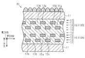
- the optical device 10 includes a base material 11, a first low refractive index region 12, a first grating region 13, a second low refractive index region 14, a second grating region 15, and a third low refractive index.
- a rate region 16 is provided.
- Each of the first low-refractive index region 12, the first lattice region 13, the second low-refractive index region 14, the second lattice region 15, and the third low-refractive index region 16 spreads in layers, and the substrate 11 They are arranged in this order from a position close to.
- the direction in which the regions are arranged is the first direction, and the first direction is the thickness direction of each region, and is the thickness direction of the optical device 10. Further, the side where the third low refractive index region 16 is located with respect to the base material 11 is the surface side of the optical device 10, and the side where the base material 11 is located with respect to the third low refractive index region 16 is the side of the optical device 10. It is the back side. Of the regions outside the optical device 10, a region located on the front surface side with respect to the base material 11 is a front surface region, and a region located on the back surface side with respect to the base material 11 is a back surface region.
- FIG. 1 shows a cross-sectional structure of the optical device 10 and shows a planar structure of the first grating region 13 and a planar structure of the second grating region 15 with these regions partially broken.
- the base material 11 has a plate shape, and the surface located on the surface side of the optical device 10 among the surfaces of the base material 11 is the surface of the base material 11.
- the selection target of the optical device 10 is light in the visible region
- the base material 11 for example, a synthetic quartz substrate or a film made of a resin such as polyethylene terephthalate or polyethylene naphthalate is used.
- the first low refractive index region 12 is in contact with the surface of the base material 11 and extends along the surface of the base material 11.
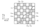
- the first lattice region 13 includes a plurality of first high refractive index portions 13a and a plurality of first low refractive index portions 13b.
- Each of the first high-refractive index portion 13a and the first low-refractive index portion 13b is viewed in a direction facing the surface of the base material 11, that is, viewed in a direction along the first direction. It has a strip shape extending along a second direction.
- the first high refractive index portions 13a and the first low refractive index portions 13b are alternately arranged along a third direction orthogonal to the second direction.
- the second direction and the third direction are directions along the surface of the substrate 11, and each of the second direction and the third direction is orthogonal to the first direction.
- the first grating region 13 is sandwiched between the first low refractive index region 12 and the second low refractive index region 14 along the first direction, and is in contact with each of these regions.
- the second grating region 15 has a plurality of second high refractive index portions 15a and a plurality of second low refractive index portions 15b.
- Each of the second high refractive index portion 15a and the second low refractive index portion 15b has a band shape extending along the second direction when viewed from the direction along the first direction, and the second high refractive index portion 15a and the second low refractive index portions 15b are alternately arranged along the third direction. That is, the extending direction of the first high refractive index portion 13a and the first low refractive index portion 13b and the extending direction of the second high refractive index portion 15a and the second low refractive index portion 15b coincide with each other.
- the second grating region 15 is sandwiched between the second low-refractive index region 14 and the third low-refractive index region 16 along the first direction, and is in contact with each of these regions.
- the planar structure of the first grating region 13 and the second grating region 15 is shown by adding dots to the first high refractive index portion 13a and the second high refractive index portion 15a.
- the first high refractive index portion 13a and the second high refractive index portion 15a are made of the same material, that is, the refractive index of the first high refractive index portion 13a and the refractive index of the second high refractive index portion 15a. Are equal to each other.
- the refractive indexes of the first high refractive index portion 13a and the second high refractive index portion 15a are higher than the refractive indexes of the first low refractive index portion 13b and the second low refractive index portion 15b.
- the refractive index of the first high refractive index portion 13a and the second high refractive index portion 15a is the same as that of each of the first low refractive index region 12, the second low refractive index region 14, and the third low refractive index region 16. It is higher than the refractive index.
- Each of the first low refractive index region 12, the second low refractive index region 14, the third low refractive index region 16, the first low refractive index portion 13b, and the second low refractive index portion 15b is made of the same material. I.e., their refractive indices are all equal.
- the refractive index of the first low refractive index region 12 is constant regardless of the portion in the region
- the refractive index of the second low refractive index region 14 is also constant regardless of the portion in the region
- the third low refractive index region 12 is low.
- the refractive index of the refractive index region 16 is also constant regardless of the region within the region.
- the length of the first high refractive index portion 13a in the third direction is the first high element width Dh1, and the length of the first low refractive index portion 13b in the third direction is the first low element width Dl1.
- the total length of the first high element width Dh1 and the first low element width Dl1 is a period of arrangement of the first high refractive index portion 13a and the first low refractive index portion 13b in the first grating region 13.
- the length of the second high refractive index portion 15a in the third direction is the second high element width Dh2, and the length of the second low refractive index portion 15b in the third direction is the second low element width Dl2.
- the total length of the second high element width Dh2 and the second low element width Dl2 is the period of the arrangement of the second high refractive index portion 15a and the second low refractive index portion 15b in the second grating region 15. Two periods P2.
- the first high element width Dh1, the first low element width Dl1, the second high element width Dh2, and the second low element width Dl2 are all equal. And the 1st period P1 and the 2nd period P2 are in agreement.
- the first period P1 and the second period P2 are smaller than the wavelength of light in the visible region, that is, each of the first period P1 and the second period P2 is a sub-wavelength period.
- the plurality of first high refractive index portions 13a in the first grating region 13 and the plurality of second high refractive index portions 15a in the second grating region 15 are guided mode resonance phenomena in the respective lattice regions.
- a sub-wavelength grating that generates The sub-wavelength grating formed by the first high refractive index portion 13a and the sub-wavelength grating formed by the second high refractive index portion 15a have the same grating period.
- the optical device 10 of the present embodiment has a structure in which two sub-wavelength gratings arranged with a gap in the first direction are embedded with a material having a lower refractive index than the material constituting these sub-wavelength gratings. ing.
- the thickness of the first lattice region 13 is the first region thickness T1
- the thickness of the second lattice region 15 is the second region thickness T2.
- the first region thickness T1 and the second region thickness T2 are the same.
- the thickness of each of the first low refractive index region 12, the second low refractive index region 14, and the third low refractive index region 16 is not particularly limited.
- the refractive index of the first grating region 13 is changed according to the volume ratio of the first high refractive index portion 13a and the first low refractive index portion 13b in the first grating region 13 to the first high refractive index portion 13a. And an average refractive index obtained by leveling the refractive index of the first low refractive index portion 13b. Since the volume ratio of the first high refractive index portion 13a and the first low refractive index portion 13b in the first grating region 13 is 1: 1, the average refractive index of the first grating region 13 is the first high refractive index portion. This is an average value of the refractive index of 13a and the refractive index of the first low refractive index portion 13b.
- the average refractive index of the second grating region 15 is the refractive index of the second high refractive index portion 15a. This is the average value of the refractive index and the refractive index of the second low refractive index portion 15 b, and coincides with the average refractive index of the first grating region 13.
- the volume ratio occupied by the first high refractive index portion 13 a in the first grating region 13 is equal to the volume ratio occupied by the second high refractive index portion 15 a in the second grating region 15.
- the refractive index of the first grating region 13 and the first low refraction that sandwiches the first grating region 13 are used.
- the difference between the refractive index of each of the refractive index region 12 and the second low refractive index region 14 is preferably larger than 0.1.
- the difference between the refractive index of the second grating region 15 and the refractive indexes of the second low refractive index region 14 and the third low refractive index region 16 sandwiching the second grating region 15 is 0.1. Is preferably larger.
- the low refractive index material may be an inorganic material such as synthetic quartz, or a polymer material such as an ultraviolet curable resin, a thermoplastic resin, or a thermosetting resin.
- a high refractive index material TiO 2 (titanium oxide), Nb 2 O 5 (niobium oxide), Ta 2 O 5 (tantalum oxide), ZrO (zirconium oxide), ZnS ( An inorganic dielectric material such as zinc sulfide) can be used.
- the optical device 10 is configured to transmit reflected light and transmitted light. Both have wavelength selectivity.
- the second grating region 15 When light enters the optical device 10 from the surface region of the optical device 10, the second grating region 15 has a sub-wavelength grating, and the second grating region 15 is lower than the refractive index of the second grating region 15. Since it is sandwiched between the second low-refractive index region 14 and the third low-refractive index region 16 having a refractive index, in the second grating region 15, the emission of diffracted light to the surface region is suppressed, and the waveguide mode A resonance phenomenon occurs. That is, light in a specific wavelength region propagates through the second grating region 15 while being multiple-reflected to cause resonance, and the light in the specific wavelength region is emitted as reflected light to the surface region of the optical device 10.
- the wavelength range of light that causes resonance in the second grating region 15 is determined by the second high element width Dh2, the second period P2, and the second region thickness T2 in the second grating region 15.
- the light of the specific wavelength region propagating through the second grating region 15 is unlikely to be multiple-reflected by the second grating region 15 without loss, and a part of the light of the specific wavelength region is Each reflection in the two-grating region 15 leaks into the second low refractive index region 14. The leaked light passes through the second low refractive index region 14 and enters the first grating region 13. Further, light in a wavelength range other than the specific wavelength range does not undergo multiple reflection at the second grating region 15, passes through the second low refractive index region 14, and enters the first grating region 13.
- the first grating region 13 When light enters the first grating region 13, the first grating region 13 has a sub-wavelength grating, and the first grating region 13 has a refractive index lower than the refractive index of the first grating region 13. Since it is sandwiched between the low refractive index region 12 and the second low refractive index region 14, the waveguide mode resonance phenomenon also occurs in the first grating region 13.
- the wavelength range of light that causes resonance in the first grating region 13 is determined by the first high element width Dh1, the first period P1, and the first region thickness T1 in the first grating region 13.
- the first high element width Dh1 coincides with the second high element width Dh2
- the first period P1 coincides with the second period P2
- the first area thickness T1 corresponds to the second region thickness T2. Therefore, the wavelength range of light that causes resonance in the first grating region 13 is the same as the wavelength range of light that causes resonance in the second grating region 15.
- the light that leaks out in the process of multiple reflection at the second grating region 15 and enters the first grating region 13 propagates while being reflected at the first grating region 13 to cause resonance, and thus the surface of the optical device 10. It is emitted as reflected light to the area. Then, the light in the wavelength region that did not cause multiple reflection in the first grating region 13 passes through the first low refractive index region 12 and the substrate 11 and exits to the back surface region of the optical device 10.
- the light in the wavelength range excluding the specific wavelength range emitted as the reflected light is emitted as the transmitted light to the back surface region of the optical device 10.
- Light is emitted to the back surface region of the optical device 10. Then, light in a wavelength range other than the wavelength range emitted as the reflected light in the wavelength range included in the incident light is emitted as a transmitted light to the surface region of the optical device 10.
- a concavo-convex structure layer 20 is formed by forming a layer made of a low refractive index material on the surface of the substrate 11 and forming a concavo-convex structure on the surface of this layer.
- the concavo-convex structure layer 20 has a flat portion 20a extending along the base material 11 and a plurality of convex portions 20b protruding from the flat portion 20a, and a plurality of concave portions which are portions located between the plurality of convex portions 20b. 20c.
- the plurality of convex portions 20b are arranged at equal intervals in the sub-wavelength period and extend in a strip shape in one direction.
- the plurality of concave portions 20c are arranged in the same pattern as the plurality of convex portions 20b, and when viewed from the direction facing the surface of the substrate 11, the total area of the plurality of convex portions 20b and the total of the plurality of concave portions 20c It is equal to the area.
- the convex portion 20b and the concave portion 20c have the arrangement period Pt of the desired first period P1 and the second period P2, and the width Dt1 of the convex part 20b is the desired first.
- the low element width Dl1 and the second high element width Dh2 are formed, and the width Dt2 of the recess 20c is formed to be the desired first high element width Dh1 and the second low element width Dl2. That is, the width Dt1 of the convex portion 20b is equal to the width Dt2 of the concave portion 20c.
- the height Ht of the convex portion 20b is formed to be larger than the desired first region thickness T1.
- a known fine processing technique such as a nanoimprint method or a dry etching method is used.
- the nanoimprint method is preferable because the fine convex portions 20b and the concave portions 20c can be easily formed.
- the ultraviolet curable resin when using the ultraviolet curable resin as the low refractive index material and forming the concavo-convex structure layer 20 by the optical nanoimprint method, first, the ultraviolet curable resin is applied to the surface of the substrate 11. Next, a synthetic quartz mold, which is an intaglio plate having irregularities that are inverted from the projections 20b and recesses 20c to be formed, is pressed against the surface of the coating layer made of an ultraviolet curable resin, and applied to the coating layer and the intaglio plate. Irradiate ultraviolet rays. Subsequently, the intaglio is released from the cured ultraviolet curable resin.
- a synthetic quartz mold which is an intaglio plate having irregularities that are inverted from the projections 20b and recesses 20c to be formed
- the unevenness of the intaglio is transferred to the ultraviolet curable resin to form the convex portions 20b and the concave portions 20c, and the convex portions 20b and the concave portions 20c and the base material 11 are made of an ultraviolet curable resin.
- a flat portion 20a is formed as the remaining film.
- a high refractive index layer 21 made of a high refractive index material is formed on the surface of the concavo-convex structure layer 20.
- a known film forming technique such as a vacuum deposition method is used.
- the high refractive index layer 21 is formed on the convex portion 20b and the concave portion 20c. That is, the high refractive index layer 21 includes a first layered portion 21a located on the concave portion 20c and a second layered portion 21b located on the convex portion 20b.
- the width Dt1 of the convex portion 20b and the width Dt2 of the concave portion 20c in the concavo-convex structure layer 20 are equal, the width Ds1 of the first layered portion 21a and the width Ds2 of the second layered portion 21b are equal. Further, the period of the arrangement of the first layered portions 21a and the period of the arrangement of the second layered portions 21b are the periods Pt, which are equal to each other. That is, the thickness of the high refractive index layer 21 is the thickness Ts1 of the first layered portion 21a and the thickness Ts2 of the second layered portion 21 and these thicknesses are equal.
- the thickness of the high refractive index layer 21 is smaller than the height Ht of the convex portion 20b, and is formed to have a desired first region thickness T1 and second region thickness T2. That is, each of the plurality of first layered portions 21a and the plurality of second layered portions 21b constitutes a sub-wavelength grating having the same pattern.
- FIG. 4 it is a layer made of the same low refractive index material as the material for forming the concavo-convex structure layer 20 so as to cover the surface of the structure made of the concavo-convex structure layer 20 and the high refractive index layer 21.
- a buried layer 22 is formed to fill the unevenness of the structure up to the second layered portion 21b.
- the buried layer 22 includes a flat portion 22a, a plurality of convex portions 22b, and a concave portion 22c located between the plurality of convex portions 22b.
- the convex portion 22b fills the space between the adjacent convex portions 20b and between the adjacent second layered portions 21b on the first layered portion 21a.
- the flat portion 22 a is located on the second layered portion 21 b and extends in a direction along the surface of the base material 11.
- the flat part 22a and the convex part 22b are connected so that the convex part 22b protrudes toward the base material 11 from the flat part 22a.
- the arrangement period of the protrusions 22b matches the arrangement period Pt of the protrusions 20b in the concavo-convex structure layer 20, the width of the protrusions 22b matches the width Dt2 of the depressions 20c, and the width of the depressions 22c It matches the width Dt1 of 20b.
- the height of the convex portion 22 b is larger than the thickness of the high refractive index layer 21.
- known film forming techniques such as various coating methods are used.
- an ultraviolet curable resin is used as the low refractive index material
- the ultraviolet curable resin is applied to the surface of the structure.
- a release plate is pressed against the surface of the coating layer made of an ultraviolet curable resin, and the coating layer is irradiated with ultraviolet rays.
- the flat plate is released from the cured ultraviolet curable resin.
- the said lithographic plate needs to be comprised with the material which permeate
- the flat portion 20 a of the concavo-convex structure layer 20 is the first low refractive index region 12.
- a first lattice region 13 is configured from the first layered portion 21a of the high refractive index layer 21 and the portion adjacent to the first layered portion 21a in the protruding portion 20b of the concavo-convex structure layer 20, and the first layered portion 21a It is the 1st high refractive index part 13a, and the part adjacent to the 1st layered part 21a in the convex part 20b is the 1st low refractive index part 13b.
- a low refractive index region 14 is formed.
- a second lattice region 15 is configured by the second layered portion 21b of the high refractive index layer 21 and a portion adjacent to the second layered portion 21b in the convex portion 22b of the buried layer 22, and the second layered portion 21b is 2 is the high refractive index portion 15a, and the portion adjacent to the second layered portion 21b in the convex portion 22b is the second low refractive index portion 15b.
- the flat portion 22 a of the buried layer 22 is the third low refractive index region 16.
- the first low refractive index region 12 and the first low refractive index portion 13b of the first grating region 13 are continuous, the first low refractive index portion 13b, 2
- the portion adjacent to the first low refractive index portion 13b in the low refractive index region 14 is continuous.
- the first low refractive index region 12, the first low refractive index portion 13b, and the portion adjacent to the first low refractive index portion 13b in the second low refractive index region 14 are one structure.
- the portion adjacent to the second low refractive index portion 15b of the second grating region 15 and the second low refractive index portion 15b are continuous, and the second low refractive index portion 15b.
- the third low refractive index region 16 are continuous.
- the portion adjacent to the second low refractive index portion 15b in the second low refractive index region 14, the second low refractive index portion 15b, and the third low refractive index region 16 are one structure.
- the reflected light obtained by emitting the light in the wavelength region enhanced by the first grating region 13 and the light in the wavelength region enhanced by the second grating region 15 is emitted.
- the strength of is increased. Therefore, in the case where the optical device 10 is formed using the nanoimprint method without precisely controlling the film thickness of the layer in contact with the first lattice region 13 or the second lattice region 15, the remaining amount is required.
- the optical device 10 with improved wavelength selectivity can be manufactured without requiring precise control of the film thickness. Therefore, manufacture of the optical device 10 is easy.
- the optical device 10 can be formed by a manufacturing method that combines an optical nanoimprint method and a vacuum vapor deposition method, and is therefore suitable for manufacturing by a roll-to-roll method. Therefore, the configuration of the optical device 10 is also suitable for mass production.
- a high refractive index material may adhere also to the side surface of the convex part 20b of the uneven structure layer 20.
- FIG. 5 in the optical device 10, the second low refractive index region 14 is adjacent to the first high refractive index portion 13 a and the second high refractive index as viewed from the direction along the first direction.
- a third high refractive index portion 17 extending in the thickness direction of the second low refractive index region 14 is included so as to connect the end portions with the refractive index portion 15a.
- the third high refractive index portion 17 may not completely connect the first high refractive index portion 13a and the second high refractive index portion 15a, and the third high refractive index portion 17 and the first high refractive index portion 17a may not be connected to each other.
- the index part 13a and the second high refractive index part 15a may be separated.
- the volume ratio of the third high refractive index portion 17 in the second low refractive index region 14 is very small.
- the portion constituted by the low refractive index material is dominant. Therefore, the refractive index of the second low refractive index region 14 is slightly larger than the refractive indexes of the first low refractive index region 12 and the third low refractive index region 16, but the first lattice region 13 and the second low refractive index region 14 It is sufficiently smaller than the refractive index of each of the grating regions 15. Accordingly, a structure suitable for the waveguide mode resonance phenomenon is realized in which each of the first grating region 13 and the second grating region 15 is sandwiched between regions having a refractive index lower than those regions.
- the concavo-convex structure layer 20 may be formed by a nanoimprint method using a thermosetting resin or a thermoplastic resin instead of the ultraviolet curable resin.
- a thermosetting resin the irradiation of ultraviolet rays may be changed to heating
- a thermoplastic resin the irradiation of ultraviolet rays may be changed to heating and cooling.
- the concavo-convex structure layer 20 is formed using a thermoplastic resin
- a material different from the thermoplastic resin is used in order to prevent the concavo-convex structure layer 20 from being heated and deformed when the buried layer 22 is formed. It is preferable to form the buried layer 22.
- the concavo-convex structure layer 20 may be formed from a thermoplastic resin, and the buried layer 22 may be formed from an ultraviolet curable resin.
- the refractive index of the low refractive index material constituting the concavo-convex structure layer 20 and the refractive index of the low refractive index material constituting the buried layer 22 may be different from each other.
- the refractive index should be lower than the refractive index of the high refractive index material constituting the high refractive index layer 21.
- the manufactured optical device 10 has a first low refractive index region. 12
- the refractive index of each of the second low refractive index region 14 and the third low refractive index region 16 is different from each other.
- the second low-refractive index region 14 has a structure in which band-shaped portions made of materials having different refractive indexes extend along the second direction and are alternately arranged along the third direction.
- the concavo-convex structure layer 20 is formed from a thermoplastic resin, and the buried layer 22 is not limited to being formed from a material different from the thermoplastic resin.
- the refractive index of the low refractive index material constituting the layer 22 may be different from each other. In short, it is sufficient that the refractive index of the low refractive index material constituting each of the concavo-convex structure layer 20 and the buried layer 22 is lower than the refractive index of the high refractive index material constituting the high refractive index layer 21.
- Each of the low refractive index regions 16 only needs to have a low refractive index.
- the base material 11 and the concavo-convex structure layer 20 may be a single continuous structure. That is, the uneven structure layer 20 is formed by forming an uneven structure on the surface of the substrate 11 made of a low refractive index material.
- an uneven structure may be formed on the surface of the base material 11 using a sheet made of a thermoplastic resin as the base material 11, or a surface of the base material 11 using a substrate made of synthetic quartz as the base material 11.
- An uneven structure may be formed on the surface.
- a well-known technique such as a dry etching method may be used to form the concavo-convex structure on the synthetic quartz substrate. In this case, in the manufactured optical device 10, the base material 11 and the first low refractive index region 12 are continuous with each other.
- the 1st application example of the optical device 10 is a form which uses the optical device 10 for a wavelength selection filter. As shown in FIG. 8, when the wavelength selection filter 50 receives incident light I1 including light of a plurality of wavelengths, the wavelength selection filter 50 reflects light I2 in a specific wavelength region and has a wavelength region other than the wavelength region of the light I2. Transmits light I3.
- the configuration of the optical device 10 is applied to the wavelength selection filter 50, and for example, it is arranged so that light enters from the surface region of the optical device 10.
- the wavelength ranges of the light I2 and the light I3 can be adjusted by setting the periods of the sub-wavelength gratings included in the first grating region 13 and the second grating region 15.
- the wavelength selection filter 50 may be used in a form that uses the light I2 that is reflected light, may be used in a form that uses the light I3 that is transmitted light, or both the light I2 and the light I3. It may be used in a form that utilizes.
- the wavelength selection filter 50 is used as a member constituting an apparatus that requires color separation, a member constituting illumination, or the like.
- the wavelength selectivity is enhanced. Therefore, by applying the configuration of the optical device 10, the wavelength selective filter 50 with enhanced wavelength selectivity can be realized. .
- the 2nd application example of the optical device 10 is a form which uses the optical device 10 for a display body.
- the display body may be used for the purpose of increasing the difficulty of counterfeiting the article, may be used for the purpose of improving the design of the article, or may be used for these purposes.
- the display body is used for authentication documents such as passports and licenses, securities such as gift certificates and checks, cards such as credit cards and cash cards, and banknotes. It is attached.
- the display body is, for example, a decorative article worn by the user, an article carried by the user, an article placed like a furniture or a household appliance, a wall or a door. It can be attached to structures.
- the display body 60 includes a front surface 60F and a back surface 60R that is a surface opposite to the front surface 60F, and the display body 60 is a first surface when viewed from the direction facing the front surface 60F. It includes a display area 61A, a second display area 61B, and a third display area 61C.
- the first display area 61A is an area where a plurality of first pixels 62A are arranged
- the second display area 61B is an area where a plurality of second pixels 62B are arranged
- the third display area 61C is an area where A region where a plurality of third pixels 62C are arranged.
- the first display area 61A is composed of a set of a plurality of first pixels 62A
- the second display area 61B is composed of a set of a plurality of second pixels 62B
- 61C is composed of a set of a plurality of third pixels 62C.
- Each of the first display area 61A, the second display area 61B, and the third display area 61C is composed of a character, a symbol, a figure, a pattern, a pattern, these, or a combination of two or more of these areas.
- a circular graphic is expressed by the first display area 61A
- a triangular graphic is expressed by the second display area 61B
- a background is expressed by the third display area 61C.
- the configuration of the optical device 10 is applied to each of the first pixel 62A, the second pixel 62B, and the third pixel 62C.
- Each of the first pixel 62A, the second pixel 62B, and the third pixel 62C has the second direction and the third direction along the surface 60F of the display body 60, that is, the display body 60.
- the elements constituting the sub-wavelength grating are arranged in a direction along the surface 60F.
- the first direction is the thickness direction of the display body 60, that is, the direction from the back surface 60R toward the front surface 60F
- the second direction and the third direction are directions along the front surface 60F.
- the pixels 62 ⁇ / b> A, 62 ⁇ / b> B, and 62 ⁇ / b> C are arranged in an orientation in which the surface area of the optical device 10 is an area facing the surface 60 ⁇ / b> F of the display body 60.
- the first period P1 of the first lattice region 13 and the second period P2 of the second lattice region 15 are different for each pixel. Therefore, the first pixel 62A, the second pixel 62B, and the third pixel 62C have different wavelength ranges in which resonance due to the waveguide mode resonance phenomenon occurs in the first grating region 13 and the second grating region 15.
- the wavelength range of the reflected light emitted from the first pixel 62A, the wavelength range of the reflected light emitted from the second pixel 62B, and the third pixel are different from each other.
- the wavelength range of the transmitted light emitted from the first pixel 62A, the wavelength range of the transmitted light emitted from the second pixel 62B, and the transmitted light emitted from the third pixel 62C are different from each other.
- the first pixel 62A is located in a region facing the surface 60F of the display body 60.
- the reflected light I4 is emitted from the second pixel 62B
- the reflected light I5 is emitted from the second pixel 62B
- the reflected light I6 is emitted from the third pixel 62C.
- the color of the hue corresponding to the wavelength range of the reflected light I4 is visually recognized in the first display area 61A, and the wavelength range of the reflected light I5 is displayed in the second display area 61B.
- the color of the hue corresponding to the wavelength range of the reflected light I6 is visually recognized in the third display area 61C. Since the wavelength range of the reflected light I4, the wavelength range of the reflected light I5, and the wavelength range of the reflected light I6 are different from each other, the first display area 61A, the second display area 61B, and the third display area 61C have different hues. Looks like the color.
- the first display of different colors is performed.
- An image composed of the area 61A, the second display area 61B, and the third display area 61C is visually recognized.
- the transmitted light I7 is emitted from the first pixel 62A to a region facing the back surface 60R of the display body 60.
- the transmitted light I8 is emitted from the second pixel 62B, and the transmitted light I9 is emitted from the third pixel 62C. Accordingly, when the back surface 60R of the display body 60 is viewed from the outside of the display body 60, the color of the hue corresponding to the wavelength range of the transmitted light I7 is visually recognized in the first display area 61A, and the transmitted light is displayed in the second display area 61B.
- the hue color corresponding to the wavelength range of I8 is visually recognized, and the color of the hue corresponding to the wavelength range of the transmitted light I9 is visually recognized in the third display area 61C. Since the wavelength range of the transmitted light I7, the wavelength range of the transmitted light I8, and the wavelength range of the transmitted light I9 are different from each other, the first display area 61A, the second display area 61B, and the third display area 61C have different hues. Looks like the color.
- the first display areas having different colors are also obtained by backside transmission observation in which the back surface 60R is observed from the back surface side of the display body 60 in a state where the incident light I1 is irradiated from the outside of the display body 60 toward the front surface 60F.
- An image composed of 61A, the second display area 61B, and the third display area 61C is visually recognized.
- the hue of the color visually recognized in the first display area 61A when the front surface 60F is viewed and when the back surface 60R is viewed is Different.
- the color visible on the back surface 60R is a color corresponding to the complementary color of the color visible on the front surface 60F.
- the hue of the color visually recognized in the second display area 61B is different, and the hue of the color visually recognized in the third display area 61C is also different.
- the wavelength selectivity is improved. Therefore, the configuration of the optical device 10 is applied to each of the pixels 62A, 62B, and 62C, whereby each display region 61A. , 61B, 61C, the vividness and brightness of the color visually recognized are enhanced. Therefore, the visibility of the image formed by the display body 60 is improved. Further, in the optical device 10 of the first embodiment, since the flexible base material 11 such as a resin film can be used, it is possible to realize the display body 60 having a high degree of freedom for shape deformation. It is.
- the base material 11, the first low refractive index region 12, the first lattice region 13, the second low refractive index region 14, and the second lattice region 15 are provided.
- the third low refractive index region 16 is continuous. That is, the first pixel 62A, the second pixel 62B, and the third pixel 62C include a common base material 11, the concavo-convex structure layer 20 that is continuous between these pixels, and a mutual relationship between these pixels. And a continuous buried layer 22.
- the concavo-convex structure layer 20 in each of the first pixel 62A, the second pixel 62B, and the third pixel 62C changes the concavo-convex cycle at the portions corresponding to the pixels 62A, 62B, and 62C using, for example, the nanoimprint method.
- the nanoimprint method By using a synthetic quartz mold, it can be formed simultaneously.
- the high refractive index layer 21 and the buried layer 22 can simultaneously form portions corresponding to the pixels 62A, 62B, and 62C. Therefore, the pixels 62A, 62B, and 62C that exhibit different colors can be easily formed.
- the number of display areas included in the display body 60 that is, the number of display areas in which pixels to which the configuration of the optical device 10 is applied is arranged and which exhibits colors of different hues is not particularly limited, and the number of display areas May be one, or four or more.
- the display body 60 includes a region having a configuration different from the configuration of the optical device 10, for example, a region having a structure in which only a flat layer made of a low refractive index material is stacked on the base material 11. Also good.
- the display area only needs to include a display element to which the configuration of the optical device 10 is applied.
- the display element is not limited to a pixel that is a minimum unit for forming a raster image, and forms a vector image. It may be an area where anchors are connected for this purpose.
- the 3rd application example of the optical device 10 is a form which uses the optical device 10 for a color filter.
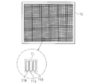
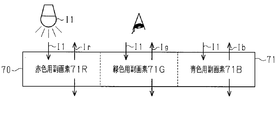
- the color filter 70 includes a plurality of pixels 71 arranged in a matrix, and each pixel 71 is composed of a red subpixel 71R, a green subpixel 71G, and a blue subpixel 71B. It consists of two subpixels.
- the color filter 70 is a reflective color filter and is provided in the display device.
- the side on which the observer who views the display surface of the display device is positioned with respect to the color filter 70 is the front side of the color filter 70, and the side opposite to the front side with respect to the color filter 70 is the back side of the color filter 70. It is.
- the color filter 70 is irradiated with light from the surface side. The intensity of the light applied to the color filter 70 can be changed for each subpixel by a liquid crystal device or the like.
- the red subpixel 71R converts the light incident on the red subpixel 71R into red light and reflects it.
- the green subpixel 71G converts the light incident on the green subpixel 71G into green light and reflects it.
- the blue subpixel 71B converts the light incident on the blue subpixel 71B into blue light and reflects it.
- the configuration of the optical device 10 is applied to each of the red subpixel 71R, the green subpixel 71G, and the blue subpixel 71B.
- Each of the red subpixel 71R, the green subpixel 71G, and the blue subpixel 71B has a second direction and a third direction along the surface of the color filter 70, that is, a display
- the elements constituting the sub-wavelength grating are arranged in a direction along the display surface of the apparatus.
- the first direction is the thickness direction of the color filter 70
- the second direction and the third direction are directions along the surface of the color filter 70.
- the sub-pixels 71R, 71G, and 71B are arranged in an orientation in which the surface area of the optical device 10 is an area on the surface side of the color filter 70.
- the red sub-pixel 71 ⁇ / b> R receives the incident light I ⁇ b> 1 including light of a plurality of wavelengths from the surface side of the color filter 70 so as to emit the red reflected light Ir.
- a first period P1 of the region 13 and a second period P2 of the second lattice region 15 are set.
- the first period P1 and the second period P2 are set so that the green subpixel 71G emits the green reflected light Ig when receiving the incident light I1.
- the first period P1 and the second period P2 are set so that the blue subpixel 71B emits the blue reflected light Ib when receiving the incident light I1.
- the wavelength selectivity is improved. Therefore, by applying the configuration of the optical device 10 to each subpixel 71R, 71G, 71B, each subpixel 71R, The vividness and brightness of colors in 71G and 71B are enhanced.
- Each of the region 13, the second low refractive index region 14, the second grating region 15, and the third low refractive index region 16 is continuous. That is, the red sub-pixel 71R, the green sub-pixel 71G, and the blue sub-pixel 71B include a common base material 11, the concavo-convex structure layer 20 that is continuous between these sub-pixels, and these sub-pixels. It has a buried layer 22 which is continuous between pixels.
- the concavo-convex structure layer 20 in each of the red subpixel 71R, the green subpixel 71G, and the blue subpixel 71B is concavo-convex at portions corresponding to the subpixels 71R, 71G, and 71B, for example, using a nanoimprint method.
- synthetic quartz molds with different periods they can be formed simultaneously.
- the high refractive index layer 21 and the buried layer 22 can simultaneously form portions corresponding to the sub-pixels 71R, 71G, and 71B. Therefore, it is possible to easily form the color filter 70 having the three types of sub-pixels 71R, 71G, and 71B.
- the combination of the colors of light extracted from the sub-pixels included in the color filter 70 may be a combination of colors different from the three colors of red, green, and blue depending on the configuration of the display device and the like.
- the effects listed below can be obtained.
- the wavelength range of light that causes resonance in the first grating region 13 matches the wavelength range of light that causes resonance in the second grating region 15. Therefore, since the light in the wavelength region strengthened in each of the two grating regions 13 and 15 is obtained as reflected light, the intensity of light emitted as reflected light compared to an optical device having only one grating region. Becomes bigger. Thereby, wavelength selectivity is improved without requiring precise control of the film thickness of the layer in contact with the grating region. That is, in the optical device, it is possible to expand the characteristics of the extracted light.
- the optical device 10 is formed by forming a buried layer made of a low refractive index material on the surface of the structure. Accordingly, since the wavelength selectivity of the optical device 10 is enhanced without requiring precise control of the film thickness of the layer in contact with the sub-wavelength grating, the optical device 10 with enhanced wavelength selectivity can be easily manufactured. it can.
- the first low refractive index region 12, the first low refractive index portion 13b, and the portion adjacent to the first low refractive index portion 13b in the second low refractive index region 14 are mutually continuous 1
- One continuous structure If it is such a structure, since each of the part which is one structure can be manufactured in one process using the above-mentioned manufacturing method, the optical device 10 can be manufactured easily.
- the waveguide mode is used in each of the grating regions 13 and 15. Since the resonance phenomenon is preferably easily generated, the intensity of the reflected light from each of the grating regions 13 and 15 is further increased. Therefore, the wavelength selectivity in the optical device 10 is further improved.
- the low refractive index material constituting each of the structures is any one of an ultraviolet curable resin, a thermosetting resin, and a thermoplastic resin, and the first high refractive index portion 13a and the second high refractive index.
- the material which comprises the part 15a contains an inorganic compound.
- the second low refractive index region 14 has a second low refractive index between the ends of the first high refractive index portion 13a and the second high refractive index portion 15a that are adjacent to each other when viewed from the direction along the first direction.
- a third high refractive index portion 17 is provided that extends along the thickness direction of the refractive index region 14.
- the structure of the optical device of 2nd Embodiment is demonstrated.
- the optical device 30 of the second embodiment includes the first low refractive index region 12, the first grating region 13, the second low refractive index region 14, and the second grating described in the first embodiment.
- Two resonance structures 18, which are structures including the region 15 and the third low refractive index region 16, are provided.
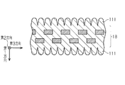
- the first resonance structure portion 18A and the second resonance structure portion 18B which are the two resonance structure portions 18, are adjacent to each other in the first direction, and the two resonance structure portions 18A and 18B are sandwiched between the two base materials 11.
- the optical device 30 of the second embodiment has a structure in which the two optical devices 10 having the configuration of the first embodiment are joined so that the third low refractive index regions 16 face each other. That is, the optical device 30 according to the second embodiment has four sub-wavelength gratings arranged in the first direction with a space therebetween, and has a structure in which these sub-wavelength gratings are embedded in a low refractive index material. .
- the side where the other base material 11 is positioned with respect to one base material 11 is the surface side of the optical device 30, and the side where the one base material 11 is positioned with respect to the other base material 11 is the back surface of the optical device 30.
- the region located on the front side with respect to the one base material 11 is the surface region, and the region located on the back side with respect to the one base material 11 This is the back area.
- the extending directions of the high refractive index portions 13a and 15a are the same. That is, all the first high refractive index portions 13a and the second high refractive index portions 15a included in the optical device 30 extend along the second direction, and all the first low refractive index portions 13b and the first high refractive index portions 13b included in the optical device 30 are included. 2
- the low refractive index portion 15b also extends along the second direction.
- the high refractive index parts 13a and 15a and the low refractive index parts 13b and 15b are located in a line along the 3rd direction alternately. That is, for the four sub-wavelength gratings included in the optical device 30, the arrangement directions of the sub-wavelength gratings are the same.
- the first high refractive index portion 13a of the first resonant structure portion 18A may overlap the first high refractive index portion 13a of the second resonant structure portion 18B, It may overlap with the second high refractive index portion 15a of the second resonant structure portion 18B, or may be part of the first high refractive index portion 13a and part of the second high refractive index portion 15a of the second resonant structure portion 18B. It may overlap.
- the first resonance structure 18A and the second resonance structure 18B may share a low refractive index region at the boundary between these.
- the third low refractive index region 16 included in the first resonance structure 18A and the third low refractive index region 16 included in the second resonance structure 18B are continuous. There is no boundary between regions.
- the first period P 1 of the first grating region 13 and the second period P 2 of the second grating region 15 are the same, and this period is the structure period Pk of the resonance structure 18. .
- the structural period Pk of the first resonant structure 18A and the structural period Pk of the second resonant structure 18B may be the same as shown in FIG. 13, or may be different from each other as shown in FIG. Good.
- the patterns of the four sub-wavelength gratings included in the optical device 30 are all the same, and the high element width Dh1, in the resonance structures 18A and 18B Dh2 is all equal, and region thicknesses T1 and T2 are all equal.
- the patterns of the four sub-wavelength gratings included in the optical device 30 are different for each resonance structure 18A and 18B. That is, the high element widths Dh1 and Dh2 are different for each of the resonance structures 18A and 18B.
- the region thicknesses T1 and T2 may all be equal, or may be different for each of the resonance structures 18A and 18B.
- the wavelength range of light causing resonance is the same in all the four grating regions 13 and 15 of the optical device 30. Therefore, when light is incident on the optical device 30 from the surface region of the optical device 30, light leaked from the grating region in the process of multiple reflection among light of a specific wavelength region that is multiple-reflected by the upper-layer lattice region. Enters the underlying lattice region and undergoes multiple reflections, and this phenomenon is repeated for the number of lattice regions. As a result, the reflected light of a specific wavelength region strengthened by each of the four grating regions 13 and 15 is emitted to the surface region of the optical device 30. Therefore, as compared with the optical device 10 of the first embodiment, the intensity of the light in the specific wavelength region emitted as the reflected light from the optical device 30 becomes larger, and thus the wavelength selectivity of the reflected light is further improved. .
- the wavelength range of light that causes resonance in the lattice regions 13 and 15 of the first resonance structure 18A, and the second resonance structure is different from each other. Therefore, when light is incident on the optical device 30 from the surface region of the optical device 30, the wavelength in which light in a specific wavelength region is multiple-reflected and not multiple-reflected in each of the grating regions 13 and 15 of the upper resonance structure portion 18.
- the light in the region passes through the resonance structure 18 and enters the lower resonance structure 18, and light in a wavelength region different from that of the upper resonance structure 18 is reflected in each lattice region 13 of the lower resonance structure 18. , 15 for multiple reflection.
- the light in the first wavelength band strengthened by the grating regions 13 and 15 included in the first resonance structure 18A and the grating region 13 included in the second resonance structure 18B. , 15 and the reflected light including the light in the second wavelength band strengthened at 15 is emitted.
- the back surface region of the optical device 30 has a wavelength region other than the first wavelength region and the second wavelength region emitted as the reflected light in the wavelength region included in the incident light to the optical device 30.
- Light is emitted as transmitted light.
- the optical device 30 it is possible to increase the wavelength range included in the reflected light while increasing the intensity of the reflected light, and to narrow the wavelength range included in the transmitted light. Therefore, the degree of freedom in adjusting the hue observed as reflected light or transmitted light can be increased through the setting of the structural period Pk in the resonance structure portions 18A and 18B.
- the configuration of the optical device 30 according to the second embodiment may be applied to the wavelength selection filter 50 or may be applied to a display element included in the display body 60, as in the application example shown in the first embodiment. However, it may be applied to the sub-pixels included in the color filter 70.
- the wavelength selectivity of the reflected light is further improved in the wavelength selection filter 50.
- the visibility of the image is enhanced by increasing the vividness and brightness of the colors visually recognized in the display areas 61A, 61B, and 61C in the surface reflection observation.
- the color filter 70 is a reflective type including the sub-pixels 71R, 71B, and 71G that emit reflected light with high monochromaticity by increasing the color clarity and luminance of the sub-pixels 71R, 71G, and 71B. The color filter 70 is realized.
- the wavelength selection filter 50 increases the degree of freedom in adjusting the hue observed as reflected light or transmitted light. It is done. Moreover, in the display body 60, the freedom degree of adjustment of the hue of the image visually recognized in surface reflection observation and back surface transmission observation is raised.
- the combination of the structural period Pk of the first resonant structure 18A and the structural period Pk of the second resonant structure 18B is mutually different. Is different.
- the combination of the structural period Pk of the first resonant structure 18A in the first pixel 62A and the structural period Pk of the second resonant structure 18B, and the structural period Pk of the first resonant structure 18A in the second pixel 62B differs in at least one of the structural period Pk of the first resonant structure 18A and the structural period Pk of the second resonant structure 18B.
- the first pixel 62A, the second pixel 62B, and the third pixel 62C have different wavelength ranges of light emitted as reflected light and different wavelength ranges of light emitted as transmitted light. ing. Thereby, in each of the front surface reflection observation and the back surface transmission observation, the first display area 61A, the second display area 61B, and the third display area 61C appear to have different hue colors. According to such a configuration, the degree of freedom in adjusting the hue of the image visually recognized in the front surface reflection observation and the rear surface transmission observation is increased.
- a transmissive color filter can be realized.
- the transmissive color filter is irradiated with light from the back side of the color filter, that is, the side opposite to the side where the observer who views the display surface of the display device is positioned, and the observer It is used in a form in which transmitted light that has passed through the color filter is viewed from the surface side of the color filter.
- the red sub-pixel 71R selectively transmits red light among the light incident on the red sub-pixel 71R.
- the green subpixel 71G selectively transmits green light among the light incident on the green subpixel 71G.
- the blue subpixel 71B selectively transmits blue light among the light incident on the blue subpixel 71B.
- a combination of the structural period Pk of the first resonant structure 18A and the structural period Pk of the second resonant structure 18B are different from each other. That is, the combination of the structural period Pk of the first resonant structure 18A in the red subpixel 71R and the structural period Pk of the second resonant structure 18B, and the structural period of the first resonant structure 18A in the green subpixel 71G.
- the combination of Pk and the structural period Pk of the second resonance structure 18B at least one of the structure period Pk of the first resonance structure 18A and the structure period Pk of the second resonance structure 18B is different. The same applies to the combination of the structural periods Pk in the green subpixel 71G and the blue subpixel 71B and the combination of the structural periods Pk in the red subpixel 71R and the blue subpixel 71B.
- the red sub-pixel 71 ⁇ / b> R emits the red transmitted light Ir to the front side when receiving the incident light I ⁇ b> 1 including light of a plurality of wavelengths from the back side of the color filter 70.
- a combination of the structural periods Pk in the resonance structure portions 18A and 18B is set. Specifically, in the red sub-pixel 71R, light in the green wavelength region is strengthened by the first resonance structure 18A and emitted as reflected light on the back surface side, and the blue wavelength is emitted by the second resonance structure 18B. The light in the area is strengthened and is emitted as reflected light on the back surface side.
- red transmitted light is emitted to the front surface side of the color filter 70, so that it is viewed from the front surface side of the color filter 70.
- red sub-pixel 71R red is visually recognized.
- the combination of the structural periods Pk in the resonance structure portions 18A and 18B is set so that the green subpixel 71G emits the green transmitted light Ig to the surface side when receiving the incident light I1. Further, the combination of the structural periods Pk in the resonance structure portions 18A and 18B is set so that the blue sub-pixel 71B emits the blue transmitted light Ib to the surface side when receiving the incident light I1.
- the intensity of incident light for each of the sub-pixels 71R, 71G, and 71B the color visually recognized as the pixel 71 is changed, and an image displayed on the display device is formed by the set of the pixels 71.
- a transmissive color filter 70 including the sub-pixels 71R, 71B, and 71G that emit transmitted light with high monochromaticity is realized.
- the manufacturing method of the optical device 30 of 2nd Embodiment is demonstrated.
- the concavo-convex structure layer 20 and the high refractive index layer 21 are sequentially formed on the substrate 11 as in the first embodiment.
- the two concavo-convex structure bodies 31, which are structures including the base material 11, the concavo-convex structure layer 20, and the high refractive index layer 21, face each other so that the high refractive index layers 21 face each other.
- these concavo-convex structures 31 are joined by filling a region between the two concavo-convex structures 31 with a low refractive index material. Thereby, the optical device 30 is formed.
- a portion formed between the two concavo-convex structures 31 by embedding with a low refractive index material is a buried layer 22.
- the ultraviolet curable resin is disposed in a region between the two concavo-convex structures 31.
- the embedded layer 22 is formed by irradiating the arranged ultraviolet curable resin with ultraviolet rays to cure the ultraviolet curable resin.
- the convex portion 22b of the burying layer 22 fills the space between the convex portion 20b and the second layered portion 21b in each of the two concavo-convex structures 31.
- the flat portion 22 a is located between the two concavo-convex structures 31 and spreads in the direction along the surface of the substrate 11.
- the flat part 22a and the convex part 22b are connected so that the convex part 22b protrudes toward the base material 11 from the flat part 22a.
- the concavo-convex structure layer 20 is constituted. A material different from the material may be used. In the two concavo-convex structures 31, the low refractive index material constituting the concavo-convex structure layer 20 and the high refractive index material constituting the high refractive index layer 21 may be different from each other.
- the first layer portions 21 a may face each other, or the first layer portion 21 a in one concavo-convex structure body 31 and the first layer portion 21 a in the other concavo-convex structure body 31.
- the two-layered portion 21b may face each other.
- the first layered portion 21a in one concavo-convex structure 31 may face part of the first layered portion 21a and part of the second layered portion 21b in the other concavo-convex structure 31.
- the optical device 30 in which the two resonance structures 18A and 18B have the same structure period Pk is obtained.
- the optical device 30 having the two resonant structure parts 18A and 18B having different structural periods Pk can be obtained. Can be formed.
- the optical device 30 may include three or more resonance structures 18 arranged in the first direction.
- the intensity of the reflected light is increased as the number of resonance structures 18 increases as long as the structure period Pk in the resonance structures 18 is the same.
- the structural periods Pk of the plurality of resonance structures 18 may be different from each other, and the plurality of resonance structures 18 and the plurality of resonance structures 18 having the same structure period Pk are different from each other in the structure period Pk.
- a resonance structure 18 may be included. According to such a configuration, it is possible to finely adjust the colors of reflected light and transmitted light emitted from the optical device 30.
- the base material 11 and the concavo-convex structure layer 20 of the concavo-convex structure 31 are formed from a material that can be formed so that the base material 11 can be peeled from the concavo-convex structure layer 20. Is done. Then, after the two concavo-convex structures 31 are joined by the low refractive index material, one of the base materials 11 is peeled off, and the exposed concavo-convex structure layer 20 and the other concavo-convex structure 31 further form a low refractive index material. By repeating the sandwiching and joining, the optical device 30 having six or more sub-wavelength gratings is formed.
- the optical device 30 includes the plurality of resonance structures 18 arranged in the first direction, since the optical device 10 includes the four or more grating regions 13 and 15, the wavelength selectivity of the optical device 30. And the degree of freedom in adjusting the wavelength range included in the reflected light and transmitted light can be increased.
- wavelength ranges included in the incident light 30 to the optical device light in the wavelength range excluding the first wavelength range and the second wavelength range emitted as the reflected light is transmitted from the optical device 10 as transmitted light. It is injected. Therefore, in the optical device 30, it is possible to widen the wavelength range included in the reflected light while increasing the intensity of the reflected light, and to narrow the wavelength range included in the transmitted light. Therefore, the degree of freedom in adjusting the hue observed as reflected light or transmitted light can be increased by setting the grating period of the sub-wavelength gratings included in each of the resonance structures 18A and 18B.
- the optical device 30 is formed by embedding two concavo-convex structures 31 so that the high refractive index layers 21 face each other and filling a region between the two concavo-convex structures 31 with a low refractive index material. Is done. According to this, the optical device 30 including a plurality of resonance structures 18 can be easily formed.
- FIG. 18 and FIG. 19 are diagrams showing a part of the optical device.
- FIG. 18 and FIG. 19 are composed of a portion made of a high refractive index material and a low refractive index material. The dots are shown with dots having different densities.
- the optical device 40 of the third embodiment includes two resonance structures 18 ⁇ / b> A and 18 ⁇ / b> B that are adjacent to each other in the first direction, similarly to the second embodiment.
- the element portions included in the lattice regions 13 and 15 of the first resonance structure portion 18A that is, the extending directions of the high refractive index portions 13a and 15a and the low refractive index portions 13b and 15b, respectively.
- the extending directions of the element portions of the lattice regions 13 and 15 of the second resonance structure portion 18B are different from each other. That is, the direction in which the element portions are arranged in the lattice regions 13 and 15 is different for each resonance structure portion 18.
- the arrangement direction of the sub-wavelength gratings included in the first resonance structure 18A is different from the arrangement direction of the sub-wavelength gratings included in the second resonance structure 18B.
- the patterns of the four sub-wavelength gratings included in the optical device 40 coincide with each other, the periods P1 and P2 are all equal in the resonance structures 18A and 18B, the high element widths Dh1 and Dh2 are all equal, and the region thickness is T1 and T2 are all equal.
- FIG. 19 is a diagram showing the optical device 40 shown in FIG. 18 divided into regions extending in the direction along the surface of the substrate 11.
- FIG. 19 is a diagram for easy understanding of the arrangement of the element portions in the two resonance structure portions 18A and 18B.
- the boundaries between the regions divided in FIG. 19 constitute the optical device 40. It does not indicate the boundary of the structure to be performed.
- the high refractive index portions 13a and 15a and the low refractive index portions 13b and 15b of the first resonance structure portion 18A extend along the second direction and are arranged along the third direction.
- the high refractive index portions 13a and 15a and the low refractive index portions 13b and 15b of the second resonance structure portion 18B extend along the third direction and are arranged along the second direction. That is, the extending direction of each element part included in the first resonance structure 18A is orthogonal to the extending direction of each element included in the second resonance structure 18B. In other words, the angle formed by the sub-wavelength grating arrangement direction of the first resonance structure 18A and the sub-wavelength grating arrangement direction of the second resonance structure 18B is 90 °.
- the sub-wavelength grating is composed of the high refractive index portions 13a and 15a extending in a band shape in one direction, in each of the grating regions 13 and 15, the light polarized in a specific direction undergoes multiple reflections and causes resonance. It is emitted as reflected light.
- the specific direction depends on the arrangement direction of the sub-wavelength gratings.
- the first resonance structure portion 18A and the second resonance structure portion 18B have different sub-wavelength grating arrangement directions, so that the lattice regions 13 and 15 of the first resonance structure portion 18A and the lattice regions of the second resonance structure portion 18B 13 and 15 are different from each other in the polarization direction of the light that is multiply reflected. Therefore, according to the optical device 40 of the third embodiment, since the reflected light is efficiently emitted with respect to the incident light including the polarization components in various directions, the intensity of the reflected light is further increased.
- the configuration of the optical device 40 according to the third embodiment may be applied to the wavelength selection filter 50 or may be applied to the display element included in the display body 60 as in the application example shown in the first embodiment. However, it may be applied to the sub-pixels included in the color filter 70.
- the incident light to the color filter 70 is light having a uniform polarization direction
- the incident light to the display body 60 is various, such as general illumination and sunlight.
- the light includes a polarization component in the direction. Therefore, the color filter 70 is highly effective when the configuration of the optical device 30 of the second embodiment is applied, and the display body 60 is effective when the configuration of the optical device 40 of the third embodiment is applied. high.
- the optical device 40 includes two concavo-convex structures 31, which are structures including the base material 11, the concavo-convex structure layer 20, and the high-refractive index layer 21.
- the layers 21 are opposed to each other so as to face each other, and a region between the two concavo-convex structures 31 is filled with a low refractive index material.
- the extending direction of the high refractive index layer 21 in one uneven structure 31 and the extending direction of the high refractive index layer 21 in the other uneven structure 31 are orthogonal to each other.
- the concavo-convex structure 31 is faced and bonded by a low refractive index material.
- the optical device 40 may include three or more resonance structure portions 18 arranged in the first direction.
- the plurality of resonance structure portions 18 include resonance structure portions 18 in which the extending directions of the element portions are different from each other. Just do it.
- Such an optical device 40 includes an even number, that is, 2n (n is an integer of 3 or more) sub-wavelength gratings, and is 2m ⁇ 1 (m is an integer of 1 to n) from the position close to one substrate 11.
- the arrangement directions are the same and the grating periods are the same.
- the optical device 40 has a structure in which a pair of sub-wavelength gratings having the same arrangement direction and the same grating period are arranged in the first direction, and these sub-wavelength gratings are embedded in a low refractive index material. Yes.
- the polarization responsiveness of the optical device 40 depends on the setting of the arrangement direction of the sub-wavelength gratings for each resonance structure 18 or the setting of the number of the resonance structures 18 having the same arrangement direction of the sub-wavelength gratings. Can also be adjusted.
- the plurality of resonance structures 18 may include resonance structures 18 having different sub-wavelength grating patterns.
- the base material 11 and the concavo-convex structure layer 20 of the concavo-convex structure 31 are formed from a material that can be formed so that the base material 11 can be peeled from the concavo-convex structure layer 20. Is done. Then, after the two concavo-convex structures 31 are joined by the low refractive index material, one of the base materials 11 is peeled off, and the exposed concavo-convex structure layer 20 and the other concavo-convex structure 31 further form a low refractive index material. By repeating the sandwiching and joining, the optical device 40 having six or more sub-wavelength gratings is formed.
- the following effects can be obtained. (12) Since the extending direction of the element part included in the first resonance structure 18A and the extending direction of the element part included in the second resonance structure 18B are different from each other, the lattice regions 13 and 15 of the first resonance structure 18A are different. In the grating regions 13 and 15 of the second resonance structure 18B, light polarized in different directions among the light included in the incident light causes resonance and is emitted from the resonance structures 18 respectively. Therefore, since the reflected light is efficiently emitted with respect to the incident light including polarization components in various directions, the intensity of the reflected light is further increased.
- the first to third embodiments can be implemented with the following modifications.
- the second low refractive index portion 15b is located above the first high refractive index portion 13a, and the first low refractive index portion 13b
- the second high refractive index portion 15a is located at the top.
- the arrangement pattern of the first high refractive index portion 13a matches the arrangement pattern of the second low refractive index portion 15b, and the arrangement pattern of the first low refractive index portion 13b is the same as the second high refractive index portion 15a. It matches the pattern of arrangement.
- the first grating region 13 In order to match the wavelength range of light that causes resonance in the first grating region 13 with the wavelength range of light that causes resonance in the second grating region 15, the first grating region 13, the second grating region 15, In which the grating periods of the sub-wavelength gratings coincide with each other, and the volume ratio of the plurality of first high refractive index portions 13a in the first grating region 13 and the volume of the plurality of second high refractive index portions 15a in the second grating region 15. The ratio needs to match.
- each of the first high refractive index portion 13a, the first low refractive index portion 13b, the second high refractive index portion 15a, and the second low refractive index portion 15b as in the above embodiments.
- the element portions have the same shape extending in a band in one common direction, and the high refractive index portions 13a and 15a and the low refractive index portions 13b and 15b extend in the lattice regions 13 and 15, respectively.
- a configuration that is alternately arranged in a direction orthogonal to the direction is easy.
- each element portion may have a shape different from the shape extending in a strip shape.
- each of the first high refractive index portion 13a, the first low refractive index portion 13b, the second high refractive index portion 15a, and the second low refractive index portion 15b is in the first direction. It has the same rectangular shape such as a square when viewed from the direction along the direction, and in each of the grating regions 13 and 15, the high refractive index portions 13a and 15a and the low refractive index portions 13b and 15b are in the second direction and the third direction.
- the configuration may be arranged alternately along each direction. In such a case, as shown in FIG. 21, in the concavo-convex structure layer 20, the convex portions 20b and the concave portions 20c are alternately arranged along each of two directions orthogonal to each other. 20c has the same rectangular shape such as a square.
- the optical device 80 according to the fourth embodiment has a structure in which an antireflection portion 112 is provided in the optical device 10 according to the first embodiment.
- the antireflection part 112 is composed of a plurality of protruding structures 111, for example.
- the plurality of protruding structures 111 are located on the surface of the third low refractive index region 16 opposite to the second lattice region 15. In other words, the plurality of protruding structures 111 are arranged on the outermost surface of the optical device 80 and constitute the outermost layer in the first direction.
- the shape of the protruding structure 111 is not particularly limited as long as the refractive index of the layered region including the protruding structure 111 is changed stepwise along the first direction.
- the cross-sectional shape along the first direction of the protruding structure 111 may be a bell shape as shown in FIG. 23, a conical shape as shown in FIG.
- the shape of the funnel turned upside down, that is, the shape of a reverse funnel may be used, or other shapes may be used.
- the protruding structure 111 is curved so that the side edge of the protruding structure 111 is recessed inward, and the width of the protruding structure 111 is narrowed from the proximal end to the distal end. This is a shape.
- the protruding structure 111 by forming the protruding structure 111 so that its width decreases as it moves away from the resonance structure portion 18 along the first direction, the refractive index of the layered region can be gradually changed. As a result, reflection at the interface between the air layer and the resonance structure 18 can be effectively suppressed.
- the size and height of the protruding structures 111 are changed, or the plurality of protruding structures 111 are aperiodically arranged.
- the material of the protruding structure 111 is mainly composed of an ultraviolet curable resin, a thermosetting resin, or a thermoplastic resin.
- the plurality of protruding structures 111 are arranged to function as the antireflection portion 112.
- the antireflection portion 112 made of the protruding structure 111 may be a separate structure from the third low-refractive index region 16 as shown in FIG. A structure integral with the refractive index region 16 may be used.
- the material of the protruding structure 111 may be made of the same resin material as that of the third low refractive index region 16 or may be made of a different resin material.
- the refractive index of the material of the protruding structure 111 is preferably 1.1 or more and 2.0 or less. Further, since the refractive index of the material of the protruding structure 111 is preferably close to the refractive index of the low refractive index material of the third low refractive index region 16, it is more preferably 1.4 or more and 1.6 or less. . Further, the difference between the refractive index of the material of the protruding structure 111 and the refractive index of the low refractive index material of the third low refractive index region 16 is preferably 0.2 or less.
- the period of the plurality of protruding structures 111 may be any period as long as it does not generate a color as interference light.
- the period of the arrangement of the plurality of protruding structures 111 is preferably 100 nm or more and 2000 nm or less, and more preferably 100 nm or more and 400 nm or less.
- the period is preferably a subwavelength period.
- the period may be a period longer than the wavelength of light in the visible region. In that case, it is preferable that the period is not constant, for example, the plurality of protruding structures 111 are arranged in a disorderly manner.
- the height along the first direction of the protruding structure 111 is preferably 100 nm or more and 2000 nm or less, and more preferably 100 nm or more and 600 nm or less.
- the aspect ratio that is the ratio of the height to the width of the protruding structure 111 is preferably 1.0 or more and 4.0 or less. As the aspect ratio increases, the antireflection effect increases, but it becomes difficult to maintain the processing accuracy of the protruding structure 111. Therefore, the aspect ratio of the protruding structure 111 is more preferably 1.5 or more and 2.0 or less.
- the protruding structure 111 may have a pillar array structure or a hole array structure, and is preferably manufactured by a roll-to-roll method.
- optical device 80 The operation of the optical device 80 according to the fourth embodiment, that is, the operation of the structure having the antireflection portion 112 will be described in comparison with the case where the antireflection portion 112 is not formed.
- the antireflection portion 112 made of the protruding structure 111 When the antireflection portion 112 made of the protruding structure 111 is not formed, when the incident light enters the optical device from the surface region, a part of the refractive index difference between the air layer and the third low refractive index region 16 Reflected due to Since the light reflected here does not pass through the resonance structure 18, unlike the reflection by the waveguide mode resonance phenomenon, normal white light is reflected when the incident light is visible light. Therefore, an observer who observes the surface region can see light in which white light reflected by the surface of the optical device is mixed with light in a specific wavelength range obtained by the resonance structure 18.
- the optical device 80 of the fourth embodiment includes an antireflection portion 112 made of a protruding structure 111 on the surface of the resonance structure portion 18. For this reason, the refractive index difference between the air layer and the third low-refractive index region 16 is changed in a stepwise manner by the protruding structure 111, and when the incident light enters the optical device 80 from the surface region, the air layer And reflection at the interface between the optical device 80 and the optical device 80 are suppressed. Therefore, in the reflected light, it is possible to prevent light in other wavelength ranges from being mixed with light in a specific wavelength range whose intensity has been increased by the resonance structure 18. Therefore, the observer can visually recognize light with higher wavelength selectivity.
- the antireflection portion 112 when the antireflection portion 112 is not present, a part of the light in the specific wavelength region reflected by the waveguide mode resonance phenomenon is reflected again between the air layer and the third low refractive index region 16, and the back surface The light is emitted to the area. That is, a part of light in the specific wavelength region does not reach the observer who observes the surface region where incident light enters.
- the antireflection portion 112 due to the presence of the antireflection portion 112, light in a specific wavelength region reflected by the guided mode resonance phenomenon is reflected on the back surface region at the interface between the air layer and the optical device 80 based on the same principle as described above. It is suppressed that it is reflected toward. That is, the presence of the antireflection portion 112 makes it possible to efficiently extract light in a specific wavelength region obtained by the guided mode resonance phenomenon.
- the antireflection part 112 should just be provided in the at least one surface of the resonance structure part 18 so that the outermost part of the optical device 80 may be comprised.
- the protruding structures 111 may be arranged on the back surface of the resonance structure 18 or may be arranged on both surfaces of the resonance structure 18 as shown in FIG. Even in such a case, the effect of suppressing reflection as described above can be obtained.
- the antireflection portion 112 is provided on the back surface of the resonance structure portion 18. In the above description, the case where the protruding structure 111 is used as the antireflection portion 112 has been described. However, if the structure has an effect of suppressing reflection, the antireflection portion 112 is different from the protruding structure 111. It may have a different structure.
- the protruding structure 111 is formed by applying a photocurable resin such as an ultraviolet curable resin to the surface of the resonance structure 18, that is, the surface of the embedded layer 22.
- the mold can be formed by pressing a mold, which is an intaglio having irregularities obtained by reversing the irregularities of the projection structure 111 to be formed, into the applied resin, and curing the photocurable resin by light irradiation.
- a known technique such as a nanoimprint method using anodized porous alumina as a mold may be applied to the formation of the protruding structure 111.
- the above-described intaglio that is, an intaglio capable of transferring the structure of the protruding structure 111 may be used instead of the flat plate when the above-described buried layer 22 is formed.
- the intaglio is pressed against a photocurable resin coated on the surface of the structure including the concavo-convex structure layer 20 and the high refractive index layer 21 to irradiate the light, whereby the embedded layer 22 and the protrusions are formed.
- the structure body 111 can be formed at the same time.
- optical device 80 may be applied to the wavelength selection filter 50 as in the application examples shown in the first to third embodiments, or may be applied to the display element included in the display body 60. Alternatively, it may be applied to a sub-pixel included in the color filter 70.
- the optical device 80 of the fourth embodiment is exemplified by the configuration in which the antireflection portion 112 is provided in the optical device 10 of the first embodiment.
- the second and third embodiments and modifications thereof are exemplified.
- the antireflection portion 112 may be provided in the example optical device.
- the antireflection portion 112 made of the protruding structure 111 may be formed on the surface of the base material 11 opposite to the resonance structure portion 18, or the base material 11 is peeled off. Then, it may be formed on the outermost surface of the resonance structure 18.
- Such a protruding structure 111 may be formed by the same method as the manufacturing method of the protruding structure 111 described above.
- FIG. 31 shows an optical device 82 having a structure in which an antireflection portion 112 is provided in the optical device 40 of the third embodiment.
- FIG. 31 exemplifies a configuration in which the antireflection portion 112 made of the protruding structure 111 is formed on both the front surface and the back surface of the optical device 82.
- the antireflection portion 112 is either the front surface or the back surface. It may be provided only on one side.
- Such a protruding structure 111 may be formed by the same method as the manufacturing method of the protruding structure 111 described above.
- the reflection preventing unit 112 suppresses reflection of incident light, transmitted light, and light in a specific wavelength region generated by the waveguide mode resonance phenomenon at the interface between the air layer and the optical device. Therefore, it is possible to efficiently extract only light in a specific wavelength region obtained by the guided mode resonance phenomenon.
- Example 1 is a wavelength selection filter to which an optical device is applied, and is a wavelength selection filter that selectively reflects light of a wavelength in the green band.
- a mold which is an intaglio used in the optical nanoimprint method was prepared. Specifically, since light having a wavelength of 365 nm was used as light to be irradiated in the optical nanoimprint method, synthetic quartz that transmits light having this wavelength was used as a mold material.
- a film made of Cr was formed on the surface of the synthetic quartz substrate by a sputtering method, and an electron beam resist pattern having a subwavelength grating pattern was formed on the Cr film by an electron beam lithography method.
- the sub-wavelength grating pattern is a pattern in which strip portions extending in one direction are arranged at equal intervals.
- the resist used was a positive type, and the film thickness was 150 nm.
- the pattern drawn by the electron beam is a pattern in which a rectangle having a short side length of 180 nm and a long side length of 3 cm is arranged in a square region having a side length of 3 cm with a period of 360 nm in the direction in which the short side extends.
- the region where the electron beam is drawn is the inner region of the rectangle.
- the Cr film in the region exposed from the resist was etched by plasma generated by applying a high frequency to a mixed gas of chlorine and oxygen.
- the synthetic quartz substrate in the region exposed from the resist and the Cr film was etched by plasma generated by applying a high frequency to ethane hexafluoride gas.
- the depth of the synthetic quartz substrate etched by this was 200 nm.
- the remaining resist and Cr film are removed, and OPTOOL HD-1100 (manufactured by Daikin Industries) is applied as a release agent to obtain a mold in which sub-wavelength grating patterns in which strip portions are arranged at equal intervals are formed in a square region. It was.
- an ultraviolet curable resin was applied to the square area where the sub-wavelength grating pattern on the mold was formed, and the mold surface was covered with a polyethylene terephthalate film subjected to an easy adhesion treatment.
- the ultraviolet curable resin was extended using a roller so as to spread over the entire surface of the square region, and the ultraviolet curable resin was cured by irradiating with 365 nm ultraviolet light, and then the polyethylene terephthalate film was peeled from the mold. Thereby, the laminated body of the uneven
- the above process was repeated to produce two laminates of the concavo-convex structure layer and the substrate. Note that the irradiation amount of ultraviolet light at 365 nm was 50 mJ / cm 2 .
- a high refractive index layer made of TiO 2 was formed by forming a TiO 2 film having a thickness of 100 nm on the surfaces of the two laminates using a vacuum deposition method. Subsequently, an ultraviolet curable resin is applied to a region where the sub-wavelength grating pattern on the surface of one of the two laminated bodies is located, and the other laminated body is applied to the coated ultraviolet curable resin. The two laminates were faced to each other so that the surfaces were in contact and the region where the sub-wavelength grating pattern was located overlapped.
- the ultraviolet curable resin was extended using a roller so as to spread over the entire surface in the region where the sub-wavelength grating pattern was located, and the ultraviolet curable resin was cured by irradiating with 365 nm ultraviolet rays to form a buried layer. Thereby, the wavelength selective filter of Example 1 was obtained. Note that the irradiation amount of ultraviolet light at 365 nm was 50 mJ / cm 2 . ⁇ Evaluation of wavelength selective filter> When reflection spectroscopy measurement of the wavelength selective filter of Example 1 was performed, a reflection spectrum having a center wavelength of about 530 nm was observed.
- Example 2 is a display body in which an optical device is applied to a pixel.
- a mold which is an intaglio used in the optical nanoimprint method was prepared. Specifically, since light having a wavelength of 365 nm was used as light to be irradiated in the optical nanoimprint method, synthetic quartz that transmits light having this wavelength was used as a mold material.
- a film made of Cr was formed on the surface of the synthetic quartz substrate by a sputtering method, and an electron beam resist pattern having a sub-wavelength grating pattern was formed on the Cr film by an electron beam lithography method.
- the sub-wavelength grating pattern is a pattern in which strip portions extending in one direction are arranged at equal intervals.
- the resist used was a positive type, and the film thickness was 150 nm.
- the pattern drawn by the electron beam is a pattern in which four types of sub-wavelength grating patterns are arranged.
- This pattern is schematically shown in FIG.
- the first pattern SP1 is a pattern in which band-shaped portions are arranged in the X direction with a period of 360 nm in a square region having a side of 3 cm.
- the second pattern SP2 is a pattern in which a band-shaped portion is arranged in a Y direction perpendicular to the X direction at a period of 360 nm in a square region having a side of 3 cm.
- the third pattern SP3 is a pattern in which band-like portions are arranged in the X direction with a period of 396 nm in a square region having a side of 3 cm.
- the fourth pattern SP4 is a pattern in which band-shaped portions are arranged in the Y direction with a period of 396 nm in a square region having a side of 3 cm.
- the Cr film exposed from the resist was etched by plasma generated by applying a high frequency to a mixed gas of chlorine and oxygen.
- the synthetic quartz substrate in the region exposed from the resist and the Cr film was etched by plasma generated by applying a high frequency to ethane hexafluoride gas.
- the depth of the synthetic quartz substrate etched by this was 200 nm.
- the remaining resist and Cr film were removed, and OPTOOL HD-1100 (manufactured by Daikin Industries) was applied as a release agent to obtain a mold in which the four sub-wavelength grating patterns were formed.
- an ultraviolet curable resin was applied in the region where the four sub-wavelength grating patterns were formed on the mold, and the mold surface was covered with a polyethylene terephthalate film subjected to an easy adhesion treatment.
- the UV curable resin is spread using a roller so as to spread over the entire surface in the region where the sub-wavelength grating pattern is formed, irradiated with 365 nm UV light to cure the UV curable resin, and then the polyethylene terephthalate film from the mold. Was peeled off.
- the sub-wavelength grating pattern obtained by inverting the four sub-wavelength grating patterns is formed on the surface of the ultraviolet curable resin, and the uneven structure layer made of the ultraviolet curable resin and the base material that is a polyethylene terephthalate film are formed.
- a laminate was obtained.
- a region where each of the four sub-wavelength grating patterns is formed corresponds to a pixel portion.
- the above process was repeated to produce two laminates of the concavo-convex structure layer and the substrate. Note that the irradiation amount of ultraviolet light at 365 nm was 50 mJ / cm 2 .
- a high refractive index layer made of TiO 2 was formed by forming a TiO 2 film having a thickness of 100 nm on the surfaces of the two laminates using a vacuum deposition method. Subsequently, an ultraviolet curable resin is applied to a region where the sub-wavelength grating pattern on the surface of one of the two laminated bodies is located, and the other laminated body is applied to the coated ultraviolet curable resin. The two laminates were opposed to each other so that the surfaces were in contact with each other and the regions where the sub-wavelength grating patterns with the same period were located overlapped.
- the ultraviolet curable resin was extended using a roller so as to spread over the entire surface in the region where the sub-wavelength grating pattern was located, and the ultraviolet curable resin was cured by irradiating with 365 nm ultraviolet rays to form a buried layer. Thereby, the display body of Example 2 was obtained. Note that the irradiation amount of ultraviolet light at 365 nm was 50 mJ / cm 2 .
- Means for solving the above-mentioned problems include the following items as technical ideas derived from the above-described embodiments and their modifications.
- a display body comprising a display element made of a material that transmits incident light and having a front surface and a back surface,
- the display element is: A plurality of first high refractive index portions constituting the first sub-wavelength grating, and a plurality of first low refractive index portions having a lower refractive index than the first high refractive index portion, along the surface First lattice regions in which the first high refractive index portions and the first low refractive index portions are alternately positioned in a direction;
- a plurality of second high-refractive-index parts that are made of the same material as the first high-refractive-index part and constitute a second sub-wavelength grating; 2 low refractive index portions, and a second grating region in which the second high refractive index portions and the second low refractive index portions are alternately positioned in a direction along the surface;
- the first lattice region is sandwiched between the first low refractive index region and the second low refractive index region in the thickness direction of the display body
- the second lattice region is sandwiched between the second low refractive index region and the third low refractive index region in the thickness direction of the display body
- the grating period of the first sub-wavelength grating and the grating period of the second sub-wavelength grating are equal to each other
- the volume ratio of the plurality of first high refractive index portions in the first grating region is the same as the volume ratio of the plurality of second high refractive index portions in the second grating region, When viewed from the direction facing the surface, the first high refractive index portion and the second low refractive index portion overlap, and the second high refractive index portion and the first low refractive index portion overlap. body.
- each grating region of the first grating region and the second grating region has a sub-wavelength grating, and each grating region has a lower refractive index than the refractive index of each grating region. Since light is incident on each grating region because it is sandwiched between the refractive index regions, emission of diffracted light into the space where the incident light enters is suppressed in each grating region, and a waveguide mode resonance phenomenon occurs. . Then, since the grating period of each grating region and the volume ratio of the high refractive index portion are the same, the wavelength range of light that causes resonance in the first grating region and the wavelength range of light that causes resonance in the second grating region Match.
- the light in a specific wavelength region that leaks out in the process of multiple reflection in one grating region and enters the other grating region propagates while being reflected in the other grating region, and from the display element, the first The reflected light in the wavelength region strengthened in the grating region and the reflected light in the wavelength region strengthened in the second grating region are emitted.
- light in a wavelength range excluding the strengthened wavelength range passes through the display element and is emitted from the display element.
- the display element having the above-described configuration the light in the wavelength region strengthened in each of the two grating regions is emitted as reflected light. Therefore, compared to the display element having only one grating region, The intensity of light in the specific wavelength range emitted as reflected light increases. Therefore, the vividness and brightness of the color visually recognized in the display area are enhanced, and as a result, the visibility of the image formed by the display body is enhanced. As a result, it is expressed by the difficulty and design of counterfeiting, that is, the appearance of the display body. Function is enhanced.
- the display body includes a plurality of display elements, and the plurality of display elements include a first display element and a second display element.
- the display body includes a first display area in which the first display element is located and a second display area in which the second display element is located, as viewed from the direction facing the surface.
- the grating periods of the first sub-wavelength grating and the second sub-wavelength grating in the first display element and the grating periods of the first sub-wavelength grating and the second sub-wavelength grating in the second display element are mutually The display object according to Item 1.
- the hues of colors visually recognized in the first display area and the second display area can be made different. Therefore, various images can be expressed by these regions.
- the difference in visible hue is realized by the difference in the grating period of the sub-wavelength grating, the difference in the manufacturing process of the display element due to the difference in color is small, and the display body can be manufactured easily.
- a portion constituted by the first grating region, the second grating region, the first low refractive index region, the second low refractive index region, and the third low refractive index region is a resonance structure portion,
- the display element since the display element includes four or more lattice regions, the wavelength selectivity of the reflected light emitted from the display element is further improved, and the wavelength range included in the reflected light and transmitted light is adjusted. It is possible to increase the degree of freedom. Therefore, the visibility of the image formed by the display body can be increased, and the degree of freedom in adjusting the hue of the image visually recognized by the display body can be increased.
- the plurality of resonance structure parts include a first resonance structure part and a second resonance structure part, and have a grating period of the first sub-wavelength grating and the second sub-wavelength grating of the first resonance structure part.
- Item 4 The display according to Item 3, wherein a first structure period and a second structure period that is a grating period of the first sub-wavelength grating and the second sub-wavelength grating included in the second resonance structure portion are different from each other.
- the wavelength range of light that causes resonance in each lattice region of the first resonance structure portion and the wavelength range of light that causes resonance in each lattice region of the second resonance structure portion are mutually different. Different. Therefore, when light is incident on the display element, light in a specific wavelength region is multiple-reflected in each lattice region of the upper resonance structure portion, and light in a wavelength region that is not multiple-reflected is transmitted through this resonance structure portion. Then, the light enters the lower resonance structure portion, and light in a wavelength region different from that of the upper resonance structure portion is multiple-reflected by each grating region of the lower resonance structure portion.
- the display element As a result, from the display element, the light in the first wavelength region strengthened in the lattice region of the first resonance structure portion and the second wavelength region intensified in the lattice region of the second resonance structure portion. Reflected light including light is emitted.
- the wavelength range included in the light incident on the display element light in the wavelength range excluding the first wavelength range and the second wavelength range emitted as the reflected light is emitted as transmitted light. Therefore, in the display element, it is possible to increase the wavelength range included in the reflected light while increasing the intensity of the reflected light, and to narrow the wavelength range included in the transmitted light.
- the degree of freedom in adjusting the hue observed as reflected light or transmitted light through the setting of the grating period of the sub-wavelength grating included in each resonance structure, and the image that is visually recognized on the display body.
- the degree of freedom in adjusting the hue of the image can be increased.
- the display body includes a plurality of display elements, and the plurality of display elements include a first display element and a second display element.
- the display body includes a first display area in which the first display element is located and a second display area in which the second display element is located, as viewed from the direction facing the surface.
- the combination of the first structure period and the second structure period in the first display element and the combination of the first structure period and the second structure period in the second display element include the first structure period.
- Item 5 The display object according to Item 4, wherein at least one of the second structural period and the second structural period is different.
- the first display element and the second display element have different wavelength ranges of light emitted as reflected light, and different wavelength ranges of light emitted as transmitted light.
- the first display area and the second display area appear to have different colors.
- freedom of adjustment of the hue of the visually recognized image is achieved. The degree is increased.
- each of the plurality of resonant structure portions the plurality of first high refractive index portions, the plurality of first low refractive index portions, the plurality of second high refractive index portions, and the plurality of second low refractive index portions.
- the element part which is each of the parts has a shape extending in a band shape in one direction
- the plurality of resonance structures include a first resonance structure and a second resonance structure,
- the display body according to Item 3 wherein a direction in which the element portion included in the first resonance structure portion extends and a direction in which the element portion included in the second resonance structure portion extends are different from each other.
- light polarized in the direction corresponding to the arrangement direction of the sub-wavelength grating among the light included in the incident light causes resonance in the grating region of each resonance structure portion. Since the arrangement directions of the sub-wavelength gratings are different between the first resonance structure portion and the second resonance structure portion, the grating region of the first resonance structure portion and the grating region of the second resonance structure portion are included in the incident light. Among the emitted light, light polarized in different directions resonates and is emitted from the respective resonance structures. Therefore, since the reflected light is efficiently emitted with respect to the incident light including polarization components in various directions, the intensity of the reflected light is further increased. Therefore, in a display body that is observed under external light including polarization components in various directions, a high effect of improving the clearness and brightness of the color visually recognized in the display area can be obtained. Designability is further improved.
- the direction in which the element portion of the first resonance structure portion extends and the direction of extension of the element portion of the second resonance structure portion are directions along the surface and are orthogonal to each other.
- the display body According to the above configuration, reflected light is more efficiently emitted with respect to incident light including polarization components in various directions.
- the display element can be easily designed and manufactured.
- the first low refractive index region, the first low refractive index portion, and a portion adjacent to the first low refractive index portion in the second low refractive index region are one continuous structure.
- a first structure that is The third low refractive index region, the second low refractive index portion, and a portion adjacent to the second low refractive index portion in the second low refractive index region are one continuous structure.
- the refractive index difference between the first structure and each of the first high refractive index portion and the second high refractive index portion is greater than 0.2
- the display body according to item 8 wherein a difference in refractive index between the second structure and each of the first high refractive index portion and the second high refractive index portion is larger than 0.2.
- the waveguide mode resonance phenomenon is preferably easily generated in each grating region, and the intensity of reflected light from each grating region is further increased. Therefore, the forgery difficulty and the design are further enhanced.
- the material constituting the first structure is one of an ultraviolet curable resin, a thermosetting resin, and a thermoplastic resin
- the material constituting the second structure is one of an ultraviolet curable resin, a thermosetting resin, and a thermoplastic resin, Item 10.
- the waveguide mode resonance phenomenon is preferably easily generated in each grating region, and the intensity of reflected light from each grating region is further increased. Therefore, the forgery difficulty and the design are further enhanced. Further, it is possible to reduce the material cost required for manufacturing the display body and to apply a simple manufacturing method such as a nanoimprint method.
- the second low refractive index region has a third high refractive index portion made of the same material as the first high refractive index portion and the second high refractive index portion, The third high refractive index portion is formed between the end portions of the first high refractive index portion and the second high refractive index portion that are adjacent to each other when viewed from the direction facing the surface.
- Item 11 The display body according to any one of Items 8 to 10, which extends along the thickness direction.
- a method of manufacturing a display body including a display element made of a material that transmits incident light the step of manufacturing the display element, A first step of forming a concavo-convex structure layer having a plurality of convex portions and a plurality of concave portions on a surface of a layer made of the first low refractive index material, wherein the plurality of convex portions are arranged in a sub-wavelength period;
- the concave portions are alternately arranged with the convex portions along a direction in which the plurality of convex portions are arranged, and the plurality of concave portions have an area equal to an area of the plurality of convex portions when viewed from a direction facing the surface.
- the first step In a second step of forming a high refractive index layer on the surface of the concavo-convex structure layer using a high refractive index material having a higher refractive index than the first low refractive index material, the high refractive index layer comprises: A second sub-wavelength grating having a thickness smaller than the height of the convex portion and positioned on the concave portion; and a second sub-wavelength grating positioned on the convex portion and having the same grating period as the first sub-wavelength grating.
- a second step comprising a subwavelength grating;
- a buried layer made of a second low refractive index material having a refractive index lower than that of the high refractive index material on the surface of the structure consisting of the uneven structure layer and the high refractive index layer, the structure
- a third step of filling the second sub-wavelength grating with the unevenness of the second sub-wavelength grating with the second low refractive index material By forming a buried layer made of a second low refractive index material having a refractive index lower than that of the high refractive index material on the surface of the structure consisting of the uneven structure layer and the high refractive index layer, the structure
- the display body that is, a display body with enhanced functions expressed by the appearance of the display body can be manufactured. And according to the said manufacturing method, since the wavelength selectivity of the reflected light inject
- the display body can be easily manufactured.
- the first step an intaglio is pressed against a coating layer made of a resin that is the first low-refractive index material, and after the resin is cured, the intaglio is released to transfer the unevenness of the intaglio to the resin.
- the high refractive index layer is formed using a material containing an inorganic compound as the high refractive index material, Item 13.
- the embedded layer is formed by applying a resin that is the second low refractive index material to the surface of the structure and curing the applied resin. Body manufacturing method.
- the concavo-convex structure layer is formed using the nanoimprint method, the concavo-convex structure layer having fine irregularities can be suitably and easily formed.
- the two structures are opposed so that the high-refractive index layers face each other, and a region between the two structures is filled with the second low-refractive index material.
- a display element having four or more sub-wavelength gratings can be easily manufactured. Therefore, it is easy to manufacture a display body including such display elements.
- a color filter comprising a plurality of sub-pixels made of a material that transmits incident light,
- the subpixel includes a plurality of resonance structures arranged in the thickness direction of the color filter,
- the resonant structure is A plurality of first high refractive index portions constituting a first sub-wavelength grating, and a plurality of first low refractive index portions having a lower refractive index than the first high refractive index portion, and the surface of the color filter
- a plurality of second high-refractive-index parts that are made of the same material as the first high-refractive-index part and constitute a second sub-wavelength grating; 2 low refractive index portions, and a second grating region in which the second high refractive index portions and the second low refractive index portions are alternately positioned in a direction along the surface;
- the first grating region is sandwiched between the first low refractive index region and the second low refractive index region in the thickness direction of the color filter
- the second grating region is sandwiched between the second low refractive index region and the third low refractive index region in the thickness direction of the color filter
- the grating period of the first sub-wavelength grating and the grating period of the second sub-wavelength grating are equal to each other
- the volume ratio of the plurality of first high refractive index portions in the first grating region is the same as the volume ratio of the plurality of second high refractive index portions in the second grating region
- the first high refractive index portion and the second low refractive index portion overlap, and the second high refractive index portion and the first low refractive index portion overlap, as viewed from the direction facing the surface. filter.
- each grating region of the first grating region and the second grating region has the sub-wavelength grating, and each grating region is lower than the refractive index of each grating region. Since it is sandwiched between low-refractive-index regions having a refractive index, when light enters each grating region, the emission of diffracted light into the space where the incident light enters is suppressed in each grating region, and the waveguide mode A resonance phenomenon occurs.
- the wavelength range of light that causes resonance in the first grating region is equal to the wavelength range of light that causes resonance in the second grating region. Match. Therefore, light in a specific wavelength region that leaks in the process of multiple reflection in one grating region and enters the other grating region propagates while being reflected in the other grating region, and is strengthened in the first grating region. The reflected light in the selected wavelength region and the reflected light in the wavelength region enhanced by the second grating region are emitted from the resonance structure portion. In the incident light, light in a wavelength range excluding the strengthened wavelength range passes through the resonant structure.
- the sub-pixel includes a plurality of resonance structures, the degree of freedom in adjusting the intensity of the reflected light to be emitted and adjusting the wavelength range of the reflected light and the transmitted light is increased. That is, it is possible to increase the intensity of light emitted from the sub-pixel and to narrow the wavelength range of light emitted from the sub-pixel, and to improve the wavelength selectivity of the sub-pixel.
- each of the plurality of resonant structure portions the plurality of first high refractive index portions, the plurality of first low refractive index portions, the plurality of second high refractive index portions, and the plurality of second low refractive index portions.
- the color filter according to item 21, wherein each of the parts has a shape extending in a band shape in one direction common to the plurality of resonance structure parts.
- each resonance structure part it is easy to match the grating period of the sub-wavelength grating and the volume ratio of the high refractive index part in each grating region.
- the sub-wavelength grating can be easily manufactured. Furthermore, it is easy to align the polarization direction of light that causes resonance in each grating region, and it is easy to realize a sub-pixel configuration that can efficiently emit reflected light with respect to incident light having a high degree of polarization.
- the grating periods of the first sub-wavelength grating and the second sub-wavelength grating included in the resonance structure part are equal to each other in the plurality of resonance structure parts,
- the plurality of sub-pixels include a first sub-pixel and a second sub-pixel, and the lattice period in the resonance structure unit included in the first sub-pixel and the resonance structure unit included in the second sub-pixel.
- Item 23. The color filter according to Item 21 or 22, wherein the grating period is different from each other.
- the wavelength range of light that causes resonance in each grating region of the subpixel is the same. Therefore, when light is incident on the subpixel, light in a specific wavelength range that is multiple-reflected by the upper grating region. Of these, light leaking from this grating region during the multiple reflection process enters the underlying grating region and undergoes multiple reflection, and this phenomenon is repeated for the number of grating regions. As a result, since the reflected light in the specific wavelength region strengthened in each grating region is emitted from the sub-pixel, the intensity of the light in the specific wavelength region emitted as reflected light becomes larger, and the wavelength of the reflected light Selectivity is further increased.
- the first subpixel and the second subpixel have different grating periods in the resonance structure portion, whereby the colors of the reflected light emitted from the first subpixel and the second subpixel can be made different.
- the color of the reflected light emitted for each sub-pixel can be made different. Since the difference in the color of the reflected light is realized by the difference in the grating period for each subpixel, the difference in the manufacturing process of the subpixel due to the difference in color is small, and the manufacture of the color filter is easy.
- the plurality of subpixels further includes a third subpixel, The grating period in the resonance structure part of the first subpixel, the grating period in the resonance structure part of the second subpixel, and the grating period in the resonance structure part of the third subpixel; Are different from each other
- the first sub-pixel selectively reflects red light
- the second sub-pixel selectively reflects green light
- the third sub-pixel selectively reflects blue light.
- a reflective color filter having sub-pixels with improved wavelength selectivity, that is, with increased intensity of reflected light to be emitted is realized. According to such a color filter, the clearness and brightness of the color in each sub-pixel can be increased.
- the plurality of resonance structure parts include a first resonance structure part and a second resonance structure part, and have a grating period of the first sub-wavelength grating and the second sub-wavelength grating of the first resonance structure part.
- a first structure period is different from a second structure period that is a grating period of the first sub-wavelength grating and the second sub-wavelength grating of the second resonance structure unit,
- the plurality of subpixels includes a first subpixel and a second subpixel, The combination of the first structure period and the second structure period in the first subpixel and the combination of the first structure period and the second structure period in the second subpixel include the first structure period.
- the wavelength range of light that causes resonance in each grating region of the first resonance structure portion and the wavelength of light that causes resonance in each grating region of the second resonance structure portion Different from each other. Therefore, when light is incident on the sub-pixel, light in a specific wavelength region is multiple-reflected in each lattice region of the upper resonance structure portion, and light in a wavelength region that is not multiple-reflected is transmitted through this resonance structure portion. Then, the light enters the lower resonance structure portion, and light in a wavelength region different from that of the upper resonance structure portion is multiple-reflected by each grating region of the lower resonance structure portion.
- the first subpixel and the second subpixel have different combinations of structural periods in the resonance structure portion, so that the colors of the transmitted light emitted from the first subpixel and the second subpixel can be made different. .
- the plurality of subpixels further includes a third subpixel,
- the combination of the first structure period and the second structure period in the first subpixel and the combination of the first structure period and the second structure period in the third subpixel include the first structure period.
- at least one of the second structural period is different,
- the combination of the first structure period and the second structure period in the second subpixel and the combination of the first structure period and the second structure period in the third subpixel include the first structure period.
- at least one of the second structural period is different, Item 25.
- the first sub-pixel selectively transmits red light
- the second sub-pixel selectively transmits green light
- the third sub-pixel selectively transmits blue light.
- the color filter described. According to the above configuration it is possible to realize a transmissive color filter that has improved wavelength selectivity, that is, includes sub-pixels that emit narrowband light as transmitted light.
- the first low refractive index region, the first low refractive index portion, and a portion adjacent to the first low refractive index portion in the second low refractive index region are one continuous structure.
- a first structure that is The third low refractive index region, the second low refractive index portion, and a portion adjacent to the second low refractive index portion in the second low refractive index region are one continuous structure.
- the refractive index difference between the first structure and each of the first high refractive index portion and the second high refractive index portion is greater than 0.2
- the material constituting the first structure is one of an ultraviolet curable resin, a thermosetting resin, and a thermoplastic resin
- the material constituting the second structure is one of an ultraviolet curable resin, a thermosetting resin, and a thermoplastic resin
- the wavelength selectivity in the sub-pixel is further improved. Further, it is possible to reduce the material cost required for manufacturing the color filter and to apply a simple manufacturing method such as a nanoimprint method.
- the second low refractive index region has a third high refractive index portion made of the same material as the first high refractive index portion and the second high refractive index portion, The third high refractive index portion is formed between the end portions of the first high refractive index portion and the second high refractive index portion that are adjacent to each other when viewed from the direction facing the surface.
- the color filter according to any one of items 21 to 29, which extends along a thickness direction of the color filter.
- a method of manufacturing a color filter including a subpixel made of a material that transmits incident light includes: A first step of forming a concavo-convex structure layer having a plurality of convex portions and a plurality of concave portions on a surface of a layer made of the first low refractive index material, wherein the plurality of convex portions are arranged in a sub-wavelength period; The concave portions are alternately arranged with the convex portions along a direction in which the plurality of convex portions are arranged, and the plurality of concave portions have an area equal to an area of the plurality of convex portions when viewed from a direction facing the surface.
- the first step In a second step of forming a high refractive index layer on the surface of the concavo-convex structure layer using a high refractive index material having a higher refractive index than the first low refractive index material, the high refractive index layer comprises: A second sub-wavelength grating having a thickness smaller than the height of the convex portion and positioned on the concave portion; and a second sub-wavelength grating positioned on the convex portion and having the same grating period as the first sub-wavelength grating.
- a second step comprising a subwavelength grating; Using two structures composed of the concavo-convex structure layer and the high refractive index layer, the two structures are opposed so that the high refractive index layers face each other, and a region between the two structures is formed. And a third step of forming a buried layer made of the second low refractive index material by filling with a second low refractive index material having a lower refractive index than the high refractive index material. .
- the above color filter that is, a color filter having improved sub-pixel wavelength selectivity can be manufactured. And according to the said manufacturing method, the color filter with which the wavelength selectivity of the subpixel was improved can be manufactured easily, without requiring control of the precise film thickness of the layer which contact
- the first step an intaglio is pressed against a coating layer made of a resin that is the first low-refractive index material, and after the resin is cured, the intaglio is released to transfer the unevenness of the intaglio to the resin.
- the high refractive index layer is formed using a material containing an inorganic compound as the high refractive index material, Item 32.
- the buried layer is formed by disposing a resin that is the second low refractive index material in a region between the two structures and curing the disposed resin. Manufacturing method of color filter.
- the concavo-convex structure layer is formed using the nanoimprint method, the concavo-convex structure layer having fine irregularities can be suitably and easily formed.
- An optical device composed of a material that transmits incident light,
- the optical device includes a resonance structure part, and an antireflection part arranged on at least one surface of the resonance structure part,
- the resonant structure is A first low refractive index region;
- a plurality of second high-refractive-index parts made of the same material as the first high-refractive-index part and constituting a second sub-wavelength grating and extending in the second direction, and lower refractive than the second high-refractive-index part
- a plurality of second low-refractive-index portions extending in the second direction having a refractive index, and second lattice regions alternately arranged in the third direction;
- the refractive index of each of the first low refractive index region, the second low refractive index region, and the third low refractive index region is an average refractive index of the first lattice region and an average refractive index of the second lattice region.
- the grating period of the first sub-wavelength grating and the grating period of the second sub-wavelength grating are equal to each other,
- the volume ratio of the plurality of first high refractive index portions in the first grating region is the same as the volume ratio of the plurality of second high refractive index portions in the second grating region, Seen from the direction facing one surface of the resonant structure,
- the first high refractive index portion and the second low refractive index portion overlap, and the second high refractive index portion and the first low refractive index portion overlap.
- the antireflection part includes a protruding structure, 42.
- Item 43 Item 43. The optical device according to Item 42, wherein the array of the protruding structures does not have periodicity.
- Item 44 Item 44. The optical device according to Item 42 or 43, wherein the size of the protruding structure is not uniform.
- the antireflection portion is located outside at least one of the plurality of resonance structure portions, the outermost resonance structure portion located in the thickness direction in the thickness direction.
- a method of manufacturing an optical device composed of a material that transmits incident light A first step of forming a concavo-convex structure layer having a plurality of convex portions and a plurality of concave portions on a surface of a layer made of the first low refractive index material, wherein the convex portions extend in a second direction; Arranged in a third direction orthogonal to two directions with a sub-wavelength period, the recesses extend in the second direction, are arranged alternately with the projections in the third direction, and the second direction in the recesses A first step in which each of the length and the width in the third direction is equal to each of the length in the second direction and the width in the third direction at the convex portion; In the second step of forming a high refractive index layer on the surface of the concavo-convex structure using a high refractive index material having a higher refractive index than the first low refractive index material, the high refractive index layer comprises: A
- a second step comprising a subwavelength grating;
- an embedded layer made of a second low refractive index material having a lower refractive index than the high refractive index material on the surface of the laminated body made of the concavo-convex structure and the high refractive index layer, the laminated body Filling the irregularities of the second sub-wavelength grating with the second low refractive index material,
- the first intaglio is pressed against a coating layer made of a resin that is the first low refractive index material, and after the resin is cured, the first intaglio is released and the first intaglio is released.
- the uneven structure layer is formed
- the high refractive index layer is formed using a material containing an inorganic compound as the high refractive index material
- the embedded layer is formed by applying a resin that is the second low-refractive index material to the surface of the laminate and curing the applied resin that is the second low-refractive index material.
- the antireflection part made of a projecting structure is formed by pressing the second intaglio to the resin disposed on the surface of the resonance structure and transferring the irregularities of the second intaglio.
- Forming, 50 A method for manufacturing an optical device according to item 49.
- the fourth step is performed simultaneously with the formation of the buried layer in the third step.
- Item 51 The method for manufacturing an optical device according to Item 49 or 50.
Abstract
光学デバイスは、第1サブ波長格子を構成する第1高屈折率部と第1低屈折率部とを有する第1格子領域、第2サブ波長格子を構成する第2高屈折率部と第2低屈折率部とを有する第2格子領域、第1低屈折率領域、第2低屈折率領域、および、第3低屈折率領域を備える。第1サブ波長格子と第2サブ波長格子との格子周期は等しく、第1格子領域と第2格子領域とにおける高屈折率部の体積比率は等しく、第1格子領域の厚さ方向に沿った方向から見て、第1高屈折率部と第2低屈折率部とが重なり、第2高屈折率部と第1低屈折率部とが重なっている。
Description
本発明は、光学デバイス、表示体、カラーフィルタ、および、光学デバイスの製造方法に関する。
モルフォ蝶の鱗粉や玉虫の表皮に代表される構造色は、色素が呈する色のように分子における電子遷移に起因して視認される色とは異なり、光の回折や干渉や散乱といった、物体の構造に起因した光学現象の作用によって視認される色である。例えば、多層膜干渉による構造色は、多層膜の各界面で反射した特定の波長域の光が干渉により強められることによって生じる構造色である。このように、多層膜干渉によって特定の波長域の光を取り出すことができるため、多層膜干渉の原理は、特定の波長域の光を選択的に透過もしくは反射することによって波長の選別を可能とする光学デバイスに利用されている。
しかしながら、多層膜干渉によって取り出すことのできる波長域は、多層膜における各層の膜厚等の層構成に依存するため、多層膜干渉を利用した光学デバイスでは、選択したい波長域ごとに、互いに異なる層構成の多層膜を形成する必要がある。したがって、選択される波長域の違いによる光学デバイスの製造工程の違いが大きいため汎用性に乏しく、また、選択される波長域が互いに異なる複数の領域を有する光学デバイスの製造工程は非常に複雑にならざるを得ない。
多層膜干渉とは異なる光学現象によって波長を選別する光学デバイスとして、導波モード共鳴現象を利用した光学デバイスが提案されている(例えば、特許文献1,2参照)。この光学デバイスは、光の波長よりも小さい周期で並ぶ回折格子であるサブ波長格子を有する。サブ波長格子に光が入射すると、入射光が入ってきた空間への回折光の射出が抑えられる一方で、特定の波長域の光が多重反射しながら伝播することにより共鳴を起こし、この特定の波長域の光が反射光として強く射出される導波モード共鳴現象が生じる。
ところで、光学デバイスとしての実用性の向上のためには、取り出される光の特性の拡張が可能であることが望ましい。例えば、反射光や透過光として射出される光の波長選択性が高いこと、すなわち、射出される光の強度が高いことや射出される光の波長域が狭いことが好ましい。また例えば、射出される光の色、すなわち、射出される光の波長域の調整の自由度が高いことが好ましい。
例えば、特許文献1に記載の光学デバイスであるカラーフィルタは、基板上にサブ波長格子を構成する複数の凸部が配置された構造を有する。しかしながら、こうした構造のデバイスにおいて、取り出される光の強度を高めるためには、特許文献1に記載のように、基板を合成石英から形成し、かつ、凸部をシリコンから形成することにより、基板と凸部との屈折率差を大きく確保して、サブ波長格子領域を伝搬する光の多重反射によるロスを小さくすることが望ましい。そのためには、合成石英からなる基板上に単結晶のSiが形成されたSOQ(Silicon on Quartz)基板を用いる必要があるため、製造コストの増大が生じる。
これに対し、特許文献2に記載の光学デバイスである波長選択素子は、基板と、サブ波長格子を構成する凸部との間に、基板を構成する材料よりも屈折率の高い材料から構成された導波層を有している。こうした構造によれば、凸部と導波層とが樹脂から形成されている場合でも、多重反射する光を導波層内に伝播させることにより、素子から出射される光の強度が高められる。また、凸部と導波層とを樹脂から形成する方法として、ナノインプリント法を用いることが可能であるため、材料費を低減しつつ簡便に素子の製造が可能であり、製造コストの削減もできる。
しかしながら、特許文献2の構造において、導波層における光の伝播モードは、主に導波層の厚みと光の波長とによって決まるため、所望の波長域の光を導波層内で多重反射させて共鳴を起こすには、導波層の膜厚を精密に制御する必要がある。微細な周期の凸部に加えて、精密な膜厚の導波層を形成することは、素子の製造に際しての負荷が大きいため、導波層によって、波長選択性を高めることには限界がある。
本発明は、取り出される光の特性の拡張が可能な光学デバイス、表示体、カラーフィルタ、および、光学デバイスの製造方法を提供することを目的とする。
上記課題を解決する光学デバイスは、入射光を透過する材料から構成された光学デバイスであって、第1サブ波長格子を構成する複数の第1高屈折率部と、前記第1高屈折率部よりも低い屈折率を有する複数の第1低屈折率部とを有し、前記第1高屈折率部の並ぶ方向に沿って前記第1高屈折率部と前記第1低屈折率部とが交互に位置する第1格子領域と、前記第1高屈折率部と同一の材料から構成されて第2サブ波長格子を構成する複数の第2高屈折率部と、前記第2高屈折率部よりも低い屈折率を有する複数の第2低屈折率部とを有し、前記第2高屈折率部の並ぶ方向に沿って前記第2高屈折率部と前記第2低屈折率部とが交互に位置する第2格子領域と、前記第1格子領域の平均屈折率および前記第2格子領域の平均屈折率の各々よりも低い屈折率をそれぞれが有する第1低屈折率領域、第2低屈折率領域、および、第3低屈折率領域と、を備え、前記第1格子領域は、当該第1格子領域の厚さ方向に前記第1低屈折率領域と前記第2低屈折率領域とに挟まれ、前記第2格子領域は、当該第2格子領域の厚さ方向に前記第2低屈折率領域と前記第3低屈折率領域とに挟まれ、前記第1サブ波長格子の格子周期と前記第2サブ波長格子の格子周期とは、相互に等しい周期であり、前記第1格子領域における前記複数の第1高屈折率部の体積比率と、前記第2格子領域における前記複数の第2高屈折率部の体積比率とは同一であり、前記第1格子領域の厚さ方向に沿った方向から見て、前記第1高屈折率部と前記第2低屈折率部とが重なり、前記第2高屈折率部と前記第1低屈折率部とが重なっている。
上記構成によれば、第1格子領域と第2格子領域との各格子領域が、サブ波長格子を有すること、および、各格子領域が、各格子領域の屈折率よりも低い屈折率を有する低屈折率領域に挟まれていることから、各格子領域に光が入射すると、各格子領域では、入射光が入ってきた空間への回折光の射出が抑えられて導波モード共鳴現象が発生する。そして、各格子領域の格子周期および高屈折率部の体積比率が同一であることにより、第1格子領域で共鳴を起こす光の波長域と第2格子領域で共鳴を起こす光の波長域とは一致する。
したがって、一方の格子領域にて多重反射する過程で漏れ出て他方の格子領域に入った特定の波長域の光は、他方の格子領域を多重反射しつつ伝播し、光学デバイスからは、第1格子領域で強められた波長域の反射光と、第2格子領域で強められた波長域の反射光とが射出される。そして、入射光のなかで上記強められた波長域を除く波長域の光が、光学デバイスを透過して、光学デバイスから射出される。
このように、上記構成の光学デバイスによれば、2つの格子領域の各々で強められた波長域の光が反射光として得られるため、1つの格子領域のみを有する光学デバイスと比較して、反射光として射出される上記特定の波長域の光の強度は大きくなる。したがって、取り出される光の特性の拡張が可能である。
上記課題を解決する光学デバイスの製造方法は、入射光を透過する材料から構成される光学デバイスの製造方法であって、第1低屈折率材料からなる層の表面に、複数の凸部と複数の凹部とを有する凹凸構造層を形成する第1工程であって、前記複数の凸部は、サブ波長周期で並び、前記凹部は、前記複数の凸部の並ぶ方向に沿って前記凸部と交互に並び、前記複数の凹部は、前記表面と対向する方向から見て前記複数の凸部の面積と等しい面積を有する、前記第1工程と、前記第1低屈折率材料よりも高い屈折率を有する高屈折率材料を用いて、前記凹凸構造層の表面に高屈折率層を形成する第2工程であって、前記高屈折率層は、前記凸部の高さよりも小さい厚さを有し、前記凹部上に位置する第1サブ波長格子と、前記凸部上に位置して前記第1サブ波長格子と同一の格子周期を有する第2サブ波長格子とを含む、前記第2工程と、前記凹凸構造層と前記高屈折率層とからなる構造体の表面に、前記高屈折率材料よりも低い屈折率を有する第2低屈折率材料からなる埋め込み層を形成することにより、前記構造体が有する凹凸を前記第2サブ波長格子上まで前記第2低屈折率材料で埋める第3工程と、を含む。
上記製法によって、上記光学デバイス、すなわち、取り出される光の特性が拡張された光学デバイスが製造できる。そして、上記製法によれば、サブ波長格子に接する層の精密な膜厚の制御を要さずに、射出される反射光の強度が高められるため、上記光学デバイスを容易に製造することができる。
本発明によれば、光学デバイスにおいて、取り出される光の特性を拡張することができる。
(第1実施形態)
図1~図7を参照して、光学デバイス、および、光学デバイスの製造方法の第1実施形態について説明する。光学デバイスは、光学デバイスに入射した光のなかから特定の波長域の光を反射、もしくは、透過することにより取り出す機能を有する。光学デバイスの選択対象の波長域は特に限定されないが、例えば、光学デバイスは、人間の肉眼で視認可能な光、すなわち、可視領域の光のなかから特定の波長域の光を取り出す。以下において、可視領域の光の波長は、400nm以上800nm以下としている。
図1~図7を参照して、光学デバイス、および、光学デバイスの製造方法の第1実施形態について説明する。光学デバイスは、光学デバイスに入射した光のなかから特定の波長域の光を反射、もしくは、透過することにより取り出す機能を有する。光学デバイスの選択対象の波長域は特に限定されないが、例えば、光学デバイスは、人間の肉眼で視認可能な光、すなわち、可視領域の光のなかから特定の波長域の光を取り出す。以下において、可視領域の光の波長は、400nm以上800nm以下としている。
[光学デバイスの構成]
図1を参照して、第1実施形態の光学デバイスの構成について説明する。図1が示すように、光学デバイス10は、基材11、第1低屈折率領域12、第1格子領域13、第2低屈折率領域14、第2格子領域15、および、第3低屈折率領域16を備えている。第1低屈折率領域12、第1格子領域13、第2低屈折率領域14、第2格子領域15、および、第3低屈折率領域16の各々は、層状に広がっており、基材11に近い位置からこの順に並んでいる。各領域の並ぶ方向が第1方向であり、第1方向は、すなわち、各領域の厚さ方向であり、光学デバイス10の厚さ方向である。また、基材11に対して第3低屈折率領域16の位置する側が光学デバイス10の表面側であり、第3低屈折率領域16に対して基材11の位置する側が、光学デバイス10の裏面側である。そして、光学デバイス10の外側の領域のなかで、基材11に対して表面側に位置する領域が表面領域であり、基材11に対して裏面側に位置する領域が裏面領域である。図1においては、光学デバイス10の断面構造を示すとともに、第1格子領域13の平面構造と第2格子領域15の平面構造とを、これらの領域を一部破断させて示している。
図1を参照して、第1実施形態の光学デバイスの構成について説明する。図1が示すように、光学デバイス10は、基材11、第1低屈折率領域12、第1格子領域13、第2低屈折率領域14、第2格子領域15、および、第3低屈折率領域16を備えている。第1低屈折率領域12、第1格子領域13、第2低屈折率領域14、第2格子領域15、および、第3低屈折率領域16の各々は、層状に広がっており、基材11に近い位置からこの順に並んでいる。各領域の並ぶ方向が第1方向であり、第1方向は、すなわち、各領域の厚さ方向であり、光学デバイス10の厚さ方向である。また、基材11に対して第3低屈折率領域16の位置する側が光学デバイス10の表面側であり、第3低屈折率領域16に対して基材11の位置する側が、光学デバイス10の裏面側である。そして、光学デバイス10の外側の領域のなかで、基材11に対して表面側に位置する領域が表面領域であり、基材11に対して裏面側に位置する領域が裏面領域である。図1においては、光学デバイス10の断面構造を示すとともに、第1格子領域13の平面構造と第2格子領域15の平面構造とを、これらの領域を一部破断させて示している。
基材11は板状を有し、基材11の有する面のうち、光学デバイス10の表面側に位置する面が基材11の表面である。光学デバイス10の選択対象が可視領域の光である場合には、基材11としては、例えば、合成石英基板や、ポリエチレンテレフタラート、ポリエチレンナフタレート等の樹脂からなるフィルムが用いられる。
第1低屈折率領域12は、基材11の表面に接し、基材11の表面に沿って広がっている。第1格子領域13は、複数の第1高屈折率部13aと複数の第1低屈折率部13bとを有する。第1高屈折率部13aと第1低屈折率部13bとの各々は、基材11の表面と対向する方向から見て、すなわち、第1方向に沿った方向から見て、1つの方向である第2方向に沿って延びる帯形状を有している。第1高屈折率部13aと第1低屈折率部13bとは、第2方向と直交する第3方向に沿って交互に並んでいる。第2方向と第3方向とは、基材11の表面に沿った方向であって、第2方向と第3方向との各々は、第1方向と直交する。第1格子領域13は、第1方向に沿って、第1低屈折率領域12と第2低屈折率領域14とに挟まれており、これらの領域の各々と接している。
第2格子領域15は、複数の第2高屈折率部15aと複数の第2低屈折率部15bとを有する。第2高屈折率部15aと第2低屈折率部15bとの各々は、第1方向に沿った方向から見て、第2方向に沿って延びる帯形状を有し、第2高屈折率部15aと第2低屈折率部15bとは、第3方向に沿って交互に並んでいる。すなわち、第1高屈折率部13aおよび第1低屈折率部13bの延びる方向と、第2高屈折率部15aおよび第2低屈折率部15bの延びる方向とは一致しており、第1高屈折率部13aおよび第1低屈折率部13bの並ぶ方向と、第2高屈折率部15aおよび第2低屈折率部15bの並ぶ方向とは一致している。そして、第1方向に沿った方向から見て、第1高屈折率部13aと第2低屈折率部15bとが重なり、第2高屈折率部15aと第1低屈折率部13bとが重なっている。第2格子領域15は、第1方向に沿って、第2低屈折率領域14と第3低屈折率領域16とに挟まれて、これらの領域の各々と接している。なお、図1においては、第1格子領域13と第2格子領域15との平面構造について、第1高屈折率部13aと第2高屈折率部15aとにドットを付して示している。
第1高屈折率部13aと第2高屈折率部15aとは、同一の材料から構成されており、すなわち、第1高屈折率部13aの屈折率と第2高屈折率部15aの屈折率とは互いに等しい。第1高屈折率部13aおよび第2高屈折率部15aの屈折率は、第1低屈折率部13b、および、第2低屈折率部15bの各々の屈折率よりも高い。さらに、第1高屈折率部13aおよび第2高屈折率部15aの屈折率は、第1低屈折率領域12、第2低屈折率領域14、および、第3低屈折率領域16の各々の屈折率よりも高い。
第1低屈折率領域12、第2低屈折率領域14、第3低屈折率領域16、第1低屈折率部13b、および、第2低屈折率部15bの各々は、同一の材料から構成されており、すなわち、これらの屈折率はすべて等しい。第1低屈折率領域12の屈折率は、領域内の部位に依らず一定であり、第2低屈折率領域14の屈折率もまた、領域内の部位に依らず一定であり、第3低屈折率領域16の屈折率もまた、領域内の部位に依らず一定である。
第3方向における第1高屈折率部13aの長さが第1高要素幅Dh1であり、第3方向における第1低屈折率部13bの長さが第1低要素幅Dl1である。第1高要素幅Dh1と第1低要素幅Dl1との合計の長さが、第1格子領域13における第1高屈折率部13aと第1低屈折率部13bとの配列の周期である第1周期P1である。
第3方向における第2高屈折率部15aの長さが第2高要素幅Dh2であり、第3方向における第2低屈折率部15bの長さが第2低要素幅Dl2である。第2高要素幅Dh2と第2低要素幅Dl2との合計の長さが、第2格子領域15における第2高屈折率部15aと第2低屈折率部15bとの配列の周期である第2周期P2である。
第1高要素幅Dh1と、第1低要素幅Dl1と、第2高要素幅Dh2と、第2低要素幅Dl2とは、すべて等しい。そして、第1周期P1と第2周期P2とは一致している。
第1周期P1と第2周期P2とは、可視領域の光の波長よりも小さく、すなわち、第1周期P1および第2周期P2の各々は、サブ波長周期である。こうした構成において、第1格子領域13における複数の第1高屈折率部13aと第2格子領域15における複数の第2高屈折率部15aとは、それぞれの格子領域にて、導波モード共鳴現象を生じさせるサブ波長格子を構成している。第1高屈折率部13aが構成するサブ波長格子と第2高屈折率部15aが構成するサブ波長格子とは、同一の格子周期を有している。すなわち、本実施形態の光学デバイス10は、第1方向に間をあけて並ぶ2つのサブ波長格子がこれらのサブ波長格子を構成する材料よりも屈折率の低い材料で埋め込まれた構造を有している。
また、第1格子領域13の厚さが、第1領域厚さT1であり、第2格子領域15の厚さが、第2領域厚さT2である。第1領域厚さT1と第2領域厚さT2とは、一致している。なお、第1低屈折率領域12、第2低屈折率領域14、および、第3低屈折率領域16の各々の厚さは特に限定されない。
上記構成において、第1格子領域13の屈折率は、第1格子領域13における第1高屈折率部13aと第1低屈折率部13bとの体積比率に応じて、第1高屈折率部13aの屈折率と第1低屈折率部13bの屈折率とを均した平均屈折率に近似される。第1格子領域13における第1高屈折率部13aと第1低屈折率部13bとの体積比率は1:1であるため、第1格子領域13の平均屈折率は、第1高屈折率部13aの屈折率と第1低屈折率部13bの屈折率との平均値である。
同様に、第2高屈折率部15aと第2低屈折率部15bとの体積比率は1:1であるため、第2格子領域15の平均屈折率は、第2高屈折率部15aの屈折率と第2低屈折率部15bの屈折率との平均値であり、第1格子領域13の平均屈折率と一致する。そして、第1格子領域13において第1高屈折率部13aが占める体積の比率と、第2格子領域15において第2高屈折率部15aが占める体積の比率とは等しい。
ここで、第1格子領域13および第2格子領域15の各々において導波モード共鳴現象を生じさせるためには、第1格子領域13の屈折率と、第1格子領域13を挟む第1低屈折率領域12および第2低屈折率領域14の各々の屈折率との差は、いずれも0.1よりも大きいことが好ましい。同様に、第2格子領域15の屈折率と、第2格子領域15を挟む第2低屈折率領域14および第3低屈折率領域16の各々の屈折率との差は、いずれも0.1よりも大きいことが好ましい。
したがって、第1高屈折率部13aおよび第2高屈折率部15aを構成する高屈折率材料の屈折率と、第1低屈折率領域12、第2低屈折率領域14、第3低屈折率領域16、第1低屈折率部13b、および、第2低屈折率部15bを構成する低屈折率材料の屈折率との差は0.2より大きいことが好ましい。
光学デバイス10の選択対象が可視領域の光である場合には、低屈折率材料としては、合成石英等の無機物や、紫外線硬化性樹脂、熱可塑性樹脂、熱硬化性樹脂等の高分子材料を用いることが可能であり、この場合、高屈折率材料としては、TiO2(酸化チタン)、Nb2O5(酸化ニオブ)、Ta2O5(酸化タンタル)、ZrO(酸化ジルコニウム)、ZnS(硫化亜鉛)等の無機誘電体材料を用いることができる。
基材11、および、各領域12,13,14,15,16のすべてが、光学デバイス10への入射光を透過する材料から構成されている場合、光学デバイス10は、反射光および透過光の両方について波長選択性を有する。
[光学デバイスの作用]
上記光学デバイス10の表面領域から光学デバイス10に光が入射すると、第2格子領域15がサブ波長格子を有すること、および、第2格子領域15が、第2格子領域15の屈折率よりも低い屈折率を有する第2低屈折率領域14と第3低屈折率領域16とに挟まれていることから、第2格子領域15では、表面領域への回折光の射出が抑えられ、導波モード共鳴現象が発生する。すなわち、特定の波長域の光が第2格子領域15を多重反射しつつ伝播して共鳴を起こし、この特定の波長域の光が、光学デバイス10の表面領域に反射光として射出される。第2格子領域15で共鳴を起こす光の波長域は、第2格子領域15における第2高要素幅Dh2、第2周期P2、および、第2領域厚さT2によって決まる。
上記光学デバイス10の表面領域から光学デバイス10に光が入射すると、第2格子領域15がサブ波長格子を有すること、および、第2格子領域15が、第2格子領域15の屈折率よりも低い屈折率を有する第2低屈折率領域14と第3低屈折率領域16とに挟まれていることから、第2格子領域15では、表面領域への回折光の射出が抑えられ、導波モード共鳴現象が発生する。すなわち、特定の波長域の光が第2格子領域15を多重反射しつつ伝播して共鳴を起こし、この特定の波長域の光が、光学デバイス10の表面領域に反射光として射出される。第2格子領域15で共鳴を起こす光の波長域は、第2格子領域15における第2高要素幅Dh2、第2周期P2、および、第2領域厚さT2によって決まる。
ここで、第2格子領域15を伝播する上記特定の波長域の光が、損失なく第2格子領域15にて多重反射することは起こりにくく、上記特定の波長域の光の一部は、第2格子領域15内での反射ごとに、第2低屈折率領域14に漏れ出る。この漏れ出た光は、第2低屈折率領域14を透過して、第1格子領域13に入る。
また、上記特定の波長域以外の波長域の光は、第2格子領域15で多重反射せずに、第2低屈折率領域14を透過して、第1格子領域13に入る。
また、上記特定の波長域以外の波長域の光は、第2格子領域15で多重反射せずに、第2低屈折率領域14を透過して、第1格子領域13に入る。
第1格子領域13に光が入射すると、第1格子領域13がサブ波長格子を有すること、および、第1格子領域13が、第1格子領域13の屈折率よりも低い屈折率を有する第1低屈折率領域12と第2低屈折率領域14とに挟まれていることから、第1格子領域13でも、導波モード共鳴現象が発生する。第1格子領域13で共鳴を起こす光の波長域は、第1格子領域13における第1高要素幅Dh1、第1周期P1、および、第1領域厚さT1によって決まる。第1格子領域13と第2格子領域15とで、第1高要素幅Dh1は第2高要素幅Dh2と一致し、第1周期P1は第2周期P2と一致し、第1領域厚さT1は第2領域厚さT2と一致する。そのため、第1格子領域13で共鳴を起こす光の波長域は、第2格子領域15で共鳴を起こす光の波長域と同じである。
したがって、第2格子領域15にて多重反射する過程で漏れ出て第1格子領域13に入った光が、第1格子領域13を多重反射しつつ伝播して共鳴を起こし、光学デバイス10の表面領域に反射光として射出される。
そして、第1格子領域13で多重反射を起こさなかった波長域の光は、第1低屈折率領域12および基材11を透過して、光学デバイス10の裏面領域に出る。
そして、第1格子領域13で多重反射を起こさなかった波長域の光は、第1低屈折率領域12および基材11を透過して、光学デバイス10の裏面領域に出る。
結果として、光学デバイス10の表面領域には、第2格子領域15で強められた波長域の光と、第1格子領域13で強められた波長域の光とが射出される。これらの光の波長域は同じであるから、1つの格子領域のみを有する光学デバイスと比較して、光学デバイス10から反射光として射出される上記特定の波長域の光の強度は大きくなる。したがって、反射光の波長選択性が高められる。
そして、光学デバイス10への入射光に含まれる波長域のなかで、上記反射光として射出された上記特定の波長域を除く波長域の光が、透過光として光学デバイス10の裏面領域に射出される。
なお、光学デバイス10の裏面領域から光学デバイス10に光が入射した場合には、第2格子領域15で強められた波長域の反射光と、第1格子領域13で強められた波長域の反射光とが、光学デバイス10の裏面領域に射出される。そして、入射光に含まれる波長域のなかで、上記反射光として射出された波長域を除く波長域の光が、透過光として光学デバイス10の表面領域に射出される。
[光学デバイスの製造方法]
図2~図4を参照して、上述した光学デバイス10の製造方法について説明する。
図2が示すように、まず、基材11の表面に、低屈折率材料からなる層を形成し、この層の表面に凹凸構造を形成することによって、凹凸構造層20を形成する。凹凸構造層20は、基材11に沿って広がる平坦部20aと、平坦部20aから突き出た複数の凸部20bとを有するとともに、複数の凸部20bの間に位置する部分である複数の凹部20cを有する。複数の凸部20bは、サブ波長周期で等間隔に配置され、1つの方向に帯状に延びる。
図2~図4を参照して、上述した光学デバイス10の製造方法について説明する。
図2が示すように、まず、基材11の表面に、低屈折率材料からなる層を形成し、この層の表面に凹凸構造を形成することによって、凹凸構造層20を形成する。凹凸構造層20は、基材11に沿って広がる平坦部20aと、平坦部20aから突き出た複数の凸部20bとを有するとともに、複数の凸部20bの間に位置する部分である複数の凹部20cを有する。複数の凸部20bは、サブ波長周期で等間隔に配置され、1つの方向に帯状に延びる。
複数の凹部20cは、複数の凸部20bと同一のパターンで並んでおり、基材11の表面と対向する方向から見て、複数の凸部20bの合計の面積と複数の凹部20cの合計の面積とは等しい。
光学デバイス10によって取り出したい波長域に応じて、凸部20bと凹部20cとは、配列の周期Ptが所望の第1周期P1かつ第2周期P2となり、凸部20bの幅Dt1が所望の第1低要素幅Dl1かつ第2高要素幅Dh2となり、凹部20cの幅Dt2が所望の第1高要素幅Dh1かつ第2低要素幅Dl2となるように形成される。すなわち、凸部20bの幅Dt1と、凹部20cの幅Dt2とは等しい。凸部20bの高さHtは、所望の第1領域厚さT1よりも大きくなるように形成される。
凹凸構造の形成には、ナノインプリント法やドライエッチング法等の公知の微細加工技術が用いられる。なかでも、ナノインプリント法は、微細な凸部20bおよび凹部20cを簡便に形成できるため好ましい。
例えば、低屈折率材料として紫外線硬化性樹脂を用い、光ナノインプリント法によって凹凸構造層20を形成する場合、まず、基材11の表面に、紫外線硬化性樹脂を塗工する。次いで、紫外線硬化性樹脂からなる塗工層の表面に、形成対象の凸部20bおよび凹部20cからなる凹凸の反転された凹凸を有する凹版である合成石英モールドを押し当て、塗工層および凹版に紫外線を照射する。続いて、硬化した紫外線硬化性樹脂から凹版を離型する。これによって、凹版の有する凹凸が紫外線硬化性樹脂に転写されて凸部20bおよび凹部20cが形成されるとともに、凸部20bおよび凹部20cと基材11との間には、紫外線硬化性樹脂からなる残膜として、平坦部20aが形成される。
次に、図3が示すように、凹凸構造層20の表面に、高屈折率材料からなる高屈折率層21を形成する。高屈折率層21の形成方法としては、真空蒸着法等の公知の成膜技術が用いられる。高屈折率層21は、凸部20b上と凹部20c上とに形成される。すなわち、高屈折率層21は、凹部20c上に位置する第1層状部21aと、凸部20b上に位置する第2層状部21bとを含む。
凹凸構造層20における凸部20bの幅Dt1と凹部20cの幅Dt2とは等しいため、第1層状部21aの幅Ds1と第2層状部21bの幅Ds2とは等しくなる。また、第1層状部21aの配列の周期と第2層状部21bの配列の周期とは周期Ptとなり、互いに等しい。高屈折率層21の厚さは、すなわち、第1層状部21aの厚さTs1であるとともに第2層状部の厚さTs2であり、これらの厚さは等しい。高屈折率層21の厚さは、凸部20bの高さHtよりも小さく、所望の第1領域厚さT1かつ第2領域厚さT2になるように形成される。すなわち、複数の第1層状部21aと複数の第2層状部21bとの各々は、互いに同一のパターンを有するサブ波長格子を構成する。
次に、図4が示すように、凹凸構造層20と高屈折率層21とからなる構造体の表面を覆うように、凹凸構造層20の形成材料と同じ低屈折率材料からなる層である埋め込み層22を形成して、上記構造体の有する凹凸を第2層状部21b上まで埋める。埋め込み層22は、平坦部22aと、複数の凸部22bと、複数の凸部22bの間に位置する凹部22cとを備える。凸部22bは、第1層状部21a上で、隣り合う凸部20bの間および隣り合う第2層状部21bの間の空間を埋めている。平坦部22aは、第2層状部21b上に位置し、基材11の表面に沿った方向に広がっている。平坦部22aと凸部22bとは、平坦部22aから凸部22bが基材11に向けて突き出るように、繋がっている。
凸部22bの配列の周期は、凹凸構造層20における凸部20bの配列の周期Ptと一致し、凸部22bの幅は、凹部20cの幅Dt2と一致し、凹部22cの幅は、凸部20bの幅Dt1と一致する。凸部22bの高さは、高屈折率層21の厚さよりも大きい。
埋め込み層22の形成方法としては、各種の塗布法等の公知の成膜技術が用いられる。例えば、低屈折率材料として紫外線硬化性樹脂を用いる場合、まず、上記構造体の表面に紫外線硬化性樹脂を塗工する。次いで、紫外線硬化性樹脂からなる塗工層の表面に、離型性を有する平板を押し当て、塗工層に紫外線を照射する。続いて、硬化した紫外線硬化性樹脂から平板を離型する。なお、紫外線硬化性樹脂を使用する場合は、上記平版は紫外線を透過する材料で構成される必要がある。
これにより、光学デバイス10が形成される。凹凸構造層20の平坦部20aが、第1低屈折率領域12である。高屈折率層21の第1層状部21aと、凹凸構造層20の凸部20bのなかで第1層状部21aに隣接する部分とから第1格子領域13が構成され、第1層状部21aが第1高屈折率部13aであり、凸部20bのなかで第1層状部21aに隣接する部分が第1低屈折率部13bである。凹凸構造層20の凸部20bのなかで第1層状部21aよりも延びている部分と、埋め込み層22の凸部22bのなかで凹凸構造層20の凸部20bに隣接する部分とから第2低屈折率領域14が構成される。
高屈折率層21の第2層状部21bと、埋め込み層22の凸部22bのなかで第2層状部21bに隣接する部分とから第2格子領域15が構成され、第2層状部21bが第2高屈折率部15aであり、凸部22bのなかで第2層状部21bに隣接する部分が第2低屈折率部15bである。埋め込み層22の平坦部22aが、第3低屈折率領域16である。
こうした製造方法によって製造される光学デバイス10においては、第1低屈折率領域12と、第1格子領域13の第1低屈折率部13bとは連続し、第1低屈折率部13bと、第2低屈折率領域14のなかで第1低屈折率部13bに隣接する部分とは連続する。第1低屈折率領域12と、第1低屈折率部13bと、第2低屈折率領域14のなかで第1低屈折率部13bに隣接する部分とは1つの構造体である。また、第2低屈折率領域14のなかで第2格子領域15の第2低屈折率部15bに隣接する部分と、第2低屈折率部15bとは連続し、第2低屈折率部15bと第3低屈折率領域16とは連続する。第2低屈折率領域14のなかで第2低屈折率部15bに隣接する部分と、第2低屈折率部15bと、第3低屈折率領域16とは1つの構造体である。
上述のように、光学デバイス10では、第1格子領域13で強められた波長域の光と、第2格子領域15で強められた波長域の光とが射出されることにより、得られる反射光の強度が大きくなる。そのため、第1格子領域13や第2格子領域15に接する層の精密な膜厚の制御を要さずに、具体的には、ナノインプリント法を用いて光学デバイス10を形成する場合には、残膜の膜厚の精密な制御を要さずに、波長選択性の高められた光学デバイス10を製造することができる。したがって、光学デバイス10の製造が容易である。
また、光学デバイス10は、光ナノインプリント法と真空蒸着法とを組み合わせた製造方法によって形成可能であるため、ロール・トゥ・ロール法による製造に適している。したがって、光学デバイス10の構成は、大量生産にも適している。
なお、真空蒸着法を用いて高屈折率層21を形成する場合、凹凸構造層20の凸部20bの側面にも、高屈折率材料が付着する場合がある。その結果、図5が示すように、光学デバイス10においては、第2低屈折率領域14が、第1方向に沿った方向から見て互いに隣り合う第1高屈折率部13aと第2高屈折率部15aとの端部間を繋ぐように、第2低屈折率領域14の厚さ方向に延びる第3高屈折率部17を含む。なお、第3高屈折率部17は、第1高屈折率部13aと第2高屈折率部15aとを完全に繋いでいなくてもよく、第3高屈折率部17と第1高屈折率部13aや第2高屈折率部15aは離れていてもよい。
第3高屈折率部17が存在する場合であっても、第2低屈折率領域14における第3高屈折率部17の体積比率は微小であって、第2低屈折率領域14においては、低屈折率材料によって構成される部分が支配的である。そのため、第2低屈折率領域14の屈折率は、第1低屈折率領域12および第3低屈折率領域16の各々の屈折率よりもわずかに大きくなるが、第1格子領域13および第2格子領域15の各々の屈折率よりは十分に小さい。したがって、第1格子領域13および第2格子領域15の各々が、これらの領域よりも屈折率の低い領域に挟まれた、導波モード共鳴現象に適した構造が実現される。
[光学デバイスの変形例]
上述の製造方法において、紫外線硬化性樹脂に代えて熱硬化性樹脂や熱可塑性樹脂を用いて、ナノインプリント法により凹凸構造層20を形成してもよい。熱硬化性樹脂を用いる場合、紫外線の照射を加熱に変更すればよく、熱可塑性樹脂を用いる場合、紫外線の照射を、加熱および冷却に変更すればよい。
上述の製造方法において、紫外線硬化性樹脂に代えて熱硬化性樹脂や熱可塑性樹脂を用いて、ナノインプリント法により凹凸構造層20を形成してもよい。熱硬化性樹脂を用いる場合、紫外線の照射を加熱に変更すればよく、熱可塑性樹脂を用いる場合、紫外線の照射を、加熱および冷却に変更すればよい。
ただし、熱可塑性樹脂を用いて凹凸構造層20を形成した場合、埋め込み層22の形成に際して、凹凸構造層20が加熱されて変形することを抑えるために、熱可塑性樹脂とは異なる材料を用いて埋め込み層22を形成することが好ましい。
例えば、図6が示すように、凹凸構造層20を熱可塑性樹脂から形成し、埋め込み層22を紫外線硬化性樹脂から形成してもよい。この場合、凹凸構造層20を構成する低屈折率材料の屈折率と、埋め込み層22を構成する低屈折率材料の屈折率とは、互いに異なっていてもよく、それぞれの低屈折率材料の屈折率が高屈折率層21を構成する高屈折率材料の屈折率よりも低ければよい。
凹凸構造層20を構成する低屈折率材料の屈折率と、埋め込み層22を構成する低屈折率材料の屈折率とが互いに異なるとき、製造された光学デバイス10においては、第1低屈折率領域12、第2低屈折率領域14、および、第3低屈折率領域16の各々の屈折率は、互いに異なる。また、第2低屈折率領域14は、互いに異なる屈折率を有する材料から構成された帯状の部分が、第2方向に沿って延び、第3方向に沿って交互に並ぶ構造を有する。
なお、凹凸構造層20を熱可塑性樹脂から形成し、埋め込み層22を熱可塑性樹脂とは異なる材料から形成する場合に限らず、凹凸構造層20を構成する低屈折率材料の屈折率と、埋め込み層22を構成する低屈折率材料の屈折率とは、互いに異なっていてもよい。要は、凹凸構造層20および埋め込み層22の各々を構成する低屈折率材料の屈折率が、高屈折率層21を構成する高屈折率材料の屈折率よりも低ければよい。そして、製造された光学デバイス10においては、第1格子領域13および第2格子領域15の屈折率の各々よりも、第1低屈折率領域12、第2低屈折率領域14、および、第3低屈折率領域16の屈折率の各々が低ければよい。
また、図7が示すように、基材11と凹凸構造層20とが互いに連続した1つの構造体であってもよい。すなわち、低屈折率材料からなる基材11の表面に凹凸構造を形成することによって、凹凸構造層20を形成する。例えば、基材11として熱可塑性樹脂からなるシートを用いて、基材11の表面に凹凸構造を形成してもよいし、基材11として合成石英からなる基板を用いて、基材11の表面に凹凸構造を形成してもよい。合成石英基板に対する凹凸構造の形成には、ドライエッチング法等の公知の技術が用いられればよい。この場合、製造された光学デバイス10においては、基材11と第1低屈折率領域12とは互いに連続している。
[光学デバイスの適用例]
上述した光学デバイス10の具体的な適用例について説明する。
<波長選択フィルタ>
光学デバイス10の第1の適用例は、光学デバイス10を波長選択フィルタに用いる形態である。図8が示すように、波長選択フィルタ50は、複数の波長の光を含む入射光I1を受けたとき、特定の波長域の光I2を反射し、この光I2の波長域を除く波長域の光I3を透過する。波長選択フィルタ50には光学デバイス10の構成が適用されており、例えば光学デバイス10の表面領域から光が入射するように配置されている。光I2および光I3の波長域は、上述のように、第1格子領域13および第2格子領域15が有するサブ波長格子の周期の設定によって調整可能である。
波長選択フィルタ50は、反射光である光I2を利用する形態で用いられてもよいし、透過光である光I3を利用する形態で用いられてもよいし、光I2と光I3との双方を利用する形態で用いられてもよい。例えば、波長選択フィルタ50は、色分解を要する装置を構成する部材や、照明を構成する部材等として用いられる。
上述のように、第1実施形態の光学デバイス10によれば波長選択性が高められるため、光学デバイス10の構成が適用されることによって、波長選択性の高められた波長選択フィルタ50が実現できる。
<表示体>
光学デバイス10の第2の適用例は、光学デバイス10を表示体に用いる形態である。表示体は、物品の偽造の困難性を高める目的で用いられてもよいし、物品の意匠性を高める目的で用いられてもよいし、これらの目的を兼ねて用いられてもよい。物品の偽造の困難性を高める目的としては、表示体は、例えば、パスポートや免許証等の認証書類、商品券や小切手等の有価証券類、クレジットカードやキャッシュカード等のカード類、紙幣等に取り付けられる。また、物品の意匠性を高める目的としては、表示体は、例えば、身に着けられる装飾品や、使用者に携帯される物品、家具や家電等のように据え置かれる物品、壁や扉等の構造物等に取り付けられる。
光学デバイス10の第2の適用例は、光学デバイス10を表示体に用いる形態である。表示体は、物品の偽造の困難性を高める目的で用いられてもよいし、物品の意匠性を高める目的で用いられてもよいし、これらの目的を兼ねて用いられてもよい。物品の偽造の困難性を高める目的としては、表示体は、例えば、パスポートや免許証等の認証書類、商品券や小切手等の有価証券類、クレジットカードやキャッシュカード等のカード類、紙幣等に取り付けられる。また、物品の意匠性を高める目的としては、表示体は、例えば、身に着けられる装飾品や、使用者に携帯される物品、家具や家電等のように据え置かれる物品、壁や扉等の構造物等に取り付けられる。
図9が示すように、表示体60は、表面60Fと、表面60Fとは反対側の面である裏面60Rとを有し、表面60Fと対向する方向から見て、表示体60は、第1表示領域61Aと第2表示領域61Bと第3表示領域61Cとを含んでいる。第1表示領域61Aは、複数の第1画素62Aが配置されている領域であり、第2表示領域61Bは、複数の第2画素62Bが配置されている領域であり、第3表示領域61Cは、複数の第3画素62Cが配置されている領域である。換言すれば、第1表示領域61Aは、複数の第1画素62Aの集合から構成されており、第2表示領域61Bは、複数の第2画素62Bの集合から構成されており、第3表示領域61Cは、複数の第3画素62Cの集合から構成されている。
第1表示領域61Aと第2表示領域61Bと第3表示領域61Cとの各々は、これらの領域単独、もしくは、これらの領域の2以上の組み合わせによって、文字、記号、図形、模様、絵柄、これらの背景等を表現する。一例として、図9に示す構成では、第1表示領域61Aによって円形の図形が表現され、第2表示領域61Bによって三角形の図形が表現され、第3表示領域61Cによって背景が表現されている。
第1画素62Aと、第2画素62Bと、第3画素62Cとの各々には、光学デバイス10の構成が適用されている。第1画素62Aと、第2画素62Bと、第3画素62Cとの各々は、第2方向と第3方向とが表示体60の表面60Fに沿った方向になるように、すなわち、表示体60の表面60Fに沿った方向にサブ波長格子を構成する要素が並ぶように配置されている。換言すれば、第1方向は、表示体60の厚さ方向、すなわち、裏面60Rから表面60Fに向かう方向であり、第2方向と第3方向とは、表面60Fに沿った方向である。例えば、これらの画素62A,62B,62Cは光学デバイス10の表面領域が表示体60の表面60Fと向かい合う領域となる向きに配置されている。
第1画素62Aと、第2画素62Bと、第3画素62Cとにおいて、第1格子領域13の第1周期P1および第2格子領域15の第2周期P2は、画素ごとに異なる周期である。したがって、第1画素62Aと、第2画素62Bと、第3画素62Cとで、第1格子領域13および第2格子領域15にて、導波モード共鳴現象による共鳴が起こる波長域は互いに異なる。
結果として、複数の波長の光を含む入射光を受けたとき、第1画素62Aから射出される反射光の波長域と、第2画素62Bから射出される反射光の波長域と、第3画素62Cから射出される光の波長域とは、互いに異なる。また、上記入射光を受けたとき、第1画素62Aから射出される透過光の波長域と、第2画素62Bから射出される透過光の波長域と、第3画素62Cから射出される透過光の波長域とは、互いに異なる。
すなわち、図10が示すように、表示体60の外側から表示体60の表面60Fに向けて入射光I1が照射されているとき、表示体60の表面60Fと向かい合う領域には、第1画素62Aから反射光I4が射出され、第2画素62Bから反射光I5が射出され、第3画素62Cから反射光I6が射出される。したがって、表示体60の外側から表面60Fを見ると、第1表示領域61Aには反射光I4の波長域に応じた色相の色が視認され、第2表示領域61Bには反射光I5の波長域に応じた色相の色が視認され、第3表示領域61Cには反射光I6の波長域に応じた色相の色が視認される。反射光I4の波長域と、反射光I5の波長域と、反射光I6の波長域とは互いに異なるため、第1表示領域61Aと第2表示領域61Bと第3表示領域61Cとは互いに異なる色相の色に見える。
したがって、表示体60の外側から表面60Fに向けて入射光I1が照射されている状態で、表示体60の表面側から表面60Fを観察する表面反射観察によれば、互いに異なる色の第1表示領域61Aと第2表示領域61Bと第3表示領域61Cとから構成される像が視認される。
また、表示体60の外側から表示体60の表面60Fに向けて入射光I1が照射されているとき、表示体60の裏面60Rと向かい合う領域には、第1画素62Aから透過光I7が射出され、第2画素62Bから透過光I8が射出され、第3画素62Cから透過光I9が射出される。したがって、表示体60の外側から表示体60の裏面60Rを見ると、第1表示領域61Aには透過光I7の波長域に応じた色相の色が視認され、第2表示領域61Bには透過光I8の波長域に応じた色相の色が視認され、第3表示領域61Cには透過光I9の波長域に応じた色相の色が視認される。透過光I7の波長域と、透過光I8の波長域と、透過光I9の波長域とは互いに異なるため、第1表示領域61Aと第2表示領域61Bと第3表示領域61Cとは互いに異なる色相の色に見える。
したがって、表示体60の外側から表面60Fに向けて入射光I1が照射されている状態で、表示体60の裏面側から裏面60Rを観察する裏面透過観察によっても、互いに異なる色の第1表示領域61Aと第2表示領域61Bと第3表示領域61Cとから構成される像が視認される。
さらに、反射光I4の波長域と透過光I7の波長域とは異なるため、表面60Fを見たときと、裏面60Rを見たときとで、第1表示領域61Aに視認される色の色相は異なる。裏面60Rに見える色は、表面60Fに見える色の補色に相当する色である。同様に、表面60Fを見たときと、裏面60Rを見たときとで、第2表示領域61Bに視認される色の色相は異なり、第3表示領域61Cに視認される色の色相も異なる。
したがって、表面反射観察と裏面透過観察とで、表示体60には互いに異なる色彩の像が視認される。それゆえ、表示体60を備える物品にて、偽造の困難性や意匠性がより高められる。また、表示体60の表裏の識別も容易である。
そして、上述のように、第1実施形態の光学デバイス10によれば波長選択性が高められるため、光学デバイス10の構成が各画素62A,62B,62Cに適用されることによって、各表示領域61A,61B,61Cに視認される色の鮮明さや明るさが高められる。それゆえ、表示体60が形成する像の視認性が高められる。また、第1実施形態の光学デバイス10では、樹脂フィルムのように可撓性のある基材11を用いることが可能であるため、形状の変形についての自由度が高い表示体60の実現も可能である。
第1画素62Aと第2画素62Bと第3画素62Cとの間で、基材11、第1低屈折率領域12、第1格子領域13、第2低屈折率領域14、第2格子領域15、および、第3低屈折率領域16の各々は連続している。すなわち、第1画素62Aと第2画素62Bと第3画素62Cとは、共通した1つの基材11と、これらの画素間で相互に連続した凹凸構造層20と、これらの画素間で相互に連続した埋め込み層22とを有している。
第1画素62Aと第2画素62Bと第3画素62Cとの各々における凹凸構造層20は、例えば、ナノインプリント法を利用して、各画素62A,62B,62Cに対応する部分で凹凸の周期を変えた合成石英モールドを用いることによって、同時に形成することができる。また、高屈折率層21および埋め込み層22も、各画素62A,62B,62Cに対応する部分を同時に形成することができる。したがって、互いに異なる色を呈する画素62A,62B,62Cを容易に形成することができる。
また、表示体60が含む表示領域の数、すなわち、光学デバイス10の構成が適用された画素が配置されて、互いに異なる色相の色を呈する表示領域の数は特に限定されず、表示領域の数は、1つであってもよいし、4つ以上であってもよい。また、表示体60は、光学デバイス10の構成とは異なる構成を有する領域、例えば、基材11に低屈折率材料からなる平坦な層のみが積層された構造を有する領域等を有していてもよい。
さらに、表示領域には、光学デバイス10の構成が適用された表示要素が含まれればよく、表示要素は、ラスタ画像を形成するための繰返しの最小単位である画素に限らず、ベクタ画像を形成するためのアンカを結んだ領域であってもよい。
<カラーフィルタ>
光学デバイス10の第3の適用例は、光学デバイス10をカラーフィルタに用いる形態である。
図11が示すように、カラーフィルタ70は、マトリックス状に並ぶ複数の画素71を備え、各画素71は、赤色用副画素71Rと、緑色用副画素71Gと、青色用副画素71Bとの3つの副画素から構成されている。
光学デバイス10の第3の適用例は、光学デバイス10をカラーフィルタに用いる形態である。
図11が示すように、カラーフィルタ70は、マトリックス状に並ぶ複数の画素71を備え、各画素71は、赤色用副画素71Rと、緑色用副画素71Gと、青色用副画素71Bとの3つの副画素から構成されている。
カラーフィルタ70は、反射型のカラーフィルタであって、表示装置に備えられる。カラーフィルタ70に対して、表示装置の表示面を見る観察者の位置する側が、カラーフィルタ70の表面側であり、カラーフィルタ70に対して、表面側と反対の側が、カラーフィルタ70の裏面側である。カラーフィルタ70には、表面側から、光が照射される。カラーフィルタ70に照射される光の強度は、副画素ごとに、液晶装置等によって変更可能に構成されている。
赤色用副画素71Rは、赤色用副画素71Rに入射した光を赤色の光に変換して反射する。緑色用副画素71Gは、緑色用副画素71Gに入射した光を緑色の光に変換して反射する。青色用副画素71Bは、青色用副画素71Bに入射した光を青色の光に変換して反射する。
赤色用副画素71Rと、緑色用副画素71Gと、青色用副画素71Bとの各々には、光学デバイス10の構成が適用されている。赤色用副画素71Rと、緑色用副画素71Gと、青色用副画素71Bとの各々は、第2方向と第3方向とがカラーフィルタ70の表面に沿った方向になるように、すなわち、表示装置の表示面に沿った方向にサブ波長格子を構成する要素が並ぶように配置されている。換言すれば、第1方向は、カラーフィルタ70の厚さ方向であり、第2方向と第3方向とは、カラーフィルタ70の表面に沿った方向である。例えば、これらの副画素71R,71G,71Bは光学デバイス10の表面領域がカラーフィルタ70の表面側の領域となる向きに配置されている。
図12が示すように、赤色用副画素71Rは、カラーフィルタ70の表面側から複数の波長の光を含む入射光I1を受けたとき、赤色の反射光Irを射出するように、第1格子領域13の第1周期P1および第2格子領域15の第2周期P2が設定されている。緑色用副画素71Gは、入射光I1を受けたとき、緑色の反射光Igを射出するように、第1周期P1および第2周期P2が設定されている。青色用副画素71Bは、入射光I1を受けたとき、青色の反射光Ibを射出するように、第1周期P1および第2周期P2が設定されている。副画素71R,71G,71Bごとに入射光の強度が変更されることによって、画素71として視認される色が変更され、画素71の集合によって表示装置の表示する像が形成される。
上述のように、第1実施形態の光学デバイス10によれば波長選択性が高められるため、光学デバイス10の構成が各副画素71R,71G,71Bに適用されることによって、各副画素71R,71G,71Bにおける色の鮮明さや輝度が高められる。
また、上述の表示体60の形態と同様に、赤色用副画素71Rと緑色用副画素71Gと青色用副画素71Bとの間で、基材11、第1低屈折率領域12、第1格子領域13、第2低屈折率領域14、第2格子領域15、および、第3低屈折率領域16の各々は連続している。すなわち、赤色用副画素71Rと緑色用副画素71Gと青色用副画素71Bとは、共通した1つの基材11と、これらの副画素間で相互に連続した凹凸構造層20と、これらの副画素間で相互に連続した埋め込み層22とを有している。
赤色用副画素71Rと緑色用副画素71Gと青色用副画素71Bとの各々における凹凸構造層20は、例えば、ナノインプリント法を用いて、各副画素71R,71G,71Bに対応する部分で凹凸の周期を変えた合成石英モールドを用いることによって、同時に形成することができる。また、高屈折率層21および埋め込み層22も、各副画素71R,71G,71Bに対応する部分を同時に形成することができる。したがって、3種類の色の副画素71R,71G,71Bを有するカラーフィルタ70を容易に形成することができる。
なお、カラーフィルタ70が備える副画素から取り出される光の色の組み合わせは、表示装置の構成等に応じて、赤、緑、青の3色とは異なる色の組み合わせであってもよい。
以上、第1実施形態によれば、以下に列挙する効果が得られる。
(1)各格子領域13,15に光が入射すると、各格子領域13,15では、導波モード共鳴現象が発生する。そして、第1格子領域13で共鳴を起こす光の波長域と第2格子領域15で共鳴を起こす光の波長域とは一致する。したがって、2つの格子領域13,15の各々で強められた波長域の光が反射光として得られるため、1つの格子領域のみを有する光学デバイスと比較して、反射光として射出される光の強度は大きくなる。これにより、格子領域に接する層の精密な膜厚の制御を要さずに、波長選択性が高められる。すなわち、光学デバイスにおいて、取り出される光の特性の拡張が可能である。
(1)各格子領域13,15に光が入射すると、各格子領域13,15では、導波モード共鳴現象が発生する。そして、第1格子領域13で共鳴を起こす光の波長域と第2格子領域15で共鳴を起こす光の波長域とは一致する。したがって、2つの格子領域13,15の各々で強められた波長域の光が反射光として得られるため、1つの格子領域のみを有する光学デバイスと比較して、反射光として射出される光の強度は大きくなる。これにより、格子領域に接する層の精密な膜厚の制御を要さずに、波長選択性が高められる。すなわち、光学デバイスにおいて、取り出される光の特性の拡張が可能である。
(2)低屈折率材料からなる凹凸構造層20を形成する工程と、凹凸構造層20の表面に高屈折率層21を形成する工程と、凹凸構造層20と高屈折率層21とからなる構造体の表面に、低屈折率材料からなる埋め込み層を形成する工程とによって、上記光学デバイス10が形成される。したがって、サブ波長格子に接する層の精密な膜厚の制御を要さずに、光学デバイス10の波長選択性が高められるため、波長選択性の高められた光学デバイス10を容易に製造することができる。
(3)特に、低屈折率材料として樹脂を用い、樹脂からなる塗工層に凹版を押し付けて樹脂の硬化によって凹凸構造層20を形成する製法では、ナノインプリント法を用いて凹凸構造層20の形成が行われるため、微細な凹凸を有する凹凸構造層20を好適に、かつ、簡便に形成することができる。
(4)第1低屈折率領域12と、第1低屈折率部13bと、第2低屈折率領域14のなかで第1低屈折率部13bに隣接する部分とが、相互に連続する1つの構造体であり、第3低屈折率領域16と、第2低屈折率部15bと、第2低屈折率領域14のなかで第2低屈折率部15bに隣接する部分とが、相互に連続する1つの構造体である。こうした構成であれば、1つの構造体である部分の各々を、上述の製造方法を用いて1つの工程にて製造することができるため、光学デバイス10の容易な製造が可能である。
(5)上記各構造体と第1高屈折率部13aおよび第2高屈折率部15aとの屈折率差が0.2よりも大きい構成では、各格子領域13,15にて、導波モード共鳴現象が好適に生じやすいため、各格子領域13,15からの反射光の強度がより高められる。したがって、光学デバイス10における波長選択性がより高められる。
(6)上記各構造体を構成する低屈折率材料が、紫外線硬化性樹脂、熱硬化性樹脂、および、熱可塑性樹脂のいずれかであり、第1高屈折率部13aおよび第2高屈折率部15aを構成する材料が、無機化合物を含む。こうした構成であれば、各格子領域13,15にて、導波モード共鳴現象が好適に生じやすいため、各格子領域13,15からの反射光の強度がより高められる。したがって、光学デバイス10における波長選択性がより高められる。また、光学デバイス10の製造に要する材料費の低減や、ナノインプリント法等の簡便な製造方法の適用が可能である。
(7)第2低屈折率領域14が、第1方向に沿った方向から見て互いに隣り合う第1高屈折率部13aと第2高屈折率部15aとの端部間で、第2低屈折率領域14の厚さ方向に沿って延びる第3高屈折率部17を備える。こうした構成であれば、真空蒸着法を利用した高屈折率部13a,15aの形成が可能であるため、サブ波長格子の好適な形成が可能である。そして、この場合であっても、導波モード共鳴現象を生じさせるための第2低屈折率領域14の構成が好適に実現される。
(第2実施形態)
図13~図16を参照して、光学デバイス、および、光学デバイスの製造方法の第2実施形態について説明する。以下では、第2実施形態と第1実施形態との相違点を中心に説明し、第1実施形態と同様の構成については同じ符号を付してその説明を省略する。
図13~図16を参照して、光学デバイス、および、光学デバイスの製造方法の第2実施形態について説明する。以下では、第2実施形態と第1実施形態との相違点を中心に説明し、第1実施形態と同様の構成については同じ符号を付してその説明を省略する。
[光学デバイスの構成]
図13および図14を参照して、第2実施形態の光学デバイスの構成について説明する。図13が示すように、第2実施形態の光学デバイス30は、第1実施形態にて説明した第1低屈折率領域12、第1格子領域13、第2低屈折率領域14、第2格子領域15、および、第3低屈折率領域16からなる構造体である共鳴構造部18を、2つ備えている。
図13および図14を参照して、第2実施形態の光学デバイスの構成について説明する。図13が示すように、第2実施形態の光学デバイス30は、第1実施形態にて説明した第1低屈折率領域12、第1格子領域13、第2低屈折率領域14、第2格子領域15、および、第3低屈折率領域16からなる構造体である共鳴構造部18を、2つ備えている。
2つの共鳴構造部18である第1共鳴構造部18Aと第2共鳴構造部18Bとは、第1方向に隣り合っており、2つの共鳴構造部18A,18Bは、2つの基材11で挟まれている。換言すれば、第2実施形態の光学デバイス30は、第1実施形態の構成を有する2つの光学デバイス10が、第3低屈折率領域16同士が向かい合うように接合された構造を有する。すなわち、第2実施形態の光学デバイス30は、第1方向に間をあけて並ぶ4つのサブ波長格子を有し、これらのサブ波長格子が低屈折率材料に埋め込まれた構造を有している。なお、一方の基材11に対して他方の基材11の位置する側が光学デバイス30の表面側であり、他方の基材11に対して一方の基材11の位置する側が光学デバイス30の裏面側である。そして、光学デバイス30の外側の領域のなかで、上記一方の基材11に対して表面側に位置する領域が表面領域であり、上記一方の基材11に対して裏面側に位置する領域が裏面領域である。
2つの共鳴構造部18A,18Bにおいて、高屈折率部13a,15aの延びる方向は一致している。すなわち、光学デバイス30が含むすべての第1高屈折率部13aおよび第2高屈折率部15aは、第2方向に沿って延び、光学デバイス30が含むすべての第1低屈折率部13bおよび第2低屈折率部15bもまた、第2方向に沿って延びている。そして、光学デバイス30が有する4つの格子領域13,15の各々にて、高屈折率部13a,15aと低屈折率部13b,15bとは、第3方向に沿って交互に並んでいる。すなわち、光学デバイス30が有する4つのサブ波長格子について、サブ波長格子の配列方向は同一である。
なお、第1方向に沿った方向から見て、第1共鳴構造部18Aの第1高屈折率部13aは、第2共鳴構造部18Bの第1高屈折率部13aと重なってもよいし、第2共鳴構造部18Bの第2高屈折率部15aと重なってもよいし、第2共鳴構造部18Bの第1高屈折率部13aの一部および第2高屈折率部15aの一部と重なってもよい。
第1共鳴構造部18Aと第2共鳴構造部18Bとは、これらの境界部分で、低屈折率領域を共有していてもよい。例えば、図13が示す例では、第1共鳴構造部18Aの備える第3低屈折率領域16と、第2共鳴構造部18Bの備える第3低屈折率領域16とは連続しており、これらの領域の境界面は存在しない。
1つの共鳴構造部18内において、第1格子領域13の第1周期P1と第2格子領域15の第2周期P2とは同一であり、この周期が当該共鳴構造部18の構造周期Pkである。
第1共鳴構造部18Aの構造周期Pkと、第2共鳴構造部18Bの構造周期Pkとは、図13が示すように同一であってもよいし、図14が示すように互いに異なっていてもよい。
2つの共鳴構造部18A,18Bが同一の構造周期Pkを有する形態においては、光学デバイス30が含む4つのサブ波長格子のパターンはすべて同一であり、共鳴構造部18A,18Bにおいて高要素幅Dh1,Dh2はすべて等しく、領域厚さT1,T2はすべて等しい。また、2つの共鳴構造部18A,18Bが互いに異なる構造周期Pkを有する形態においては、光学デバイス30が含む4つのサブ波長格子のパターンは共鳴構造部18A,18Bごとに異なる。すなわち、高要素幅Dh1,Dh2は共鳴構造部18A,18Bごとに異なる。領域厚さT1,T2はすべて等しくてもよいし、共鳴構造部18A,18Bごとに異なってもよい。
[光学デバイスの作用]
2つの共鳴構造部18A,18Bが同一の構造周期Pkを有する構成では、光学デバイス30が有する4つの格子領域13,15のすべてにおいて、共鳴を起こす光の波長域は一致する。したがって、光学デバイス30の表面領域から光学デバイス30に光が入射したとき、上層の格子領域にて多重反射する特定の波長域の光のうち、多重反射の過程でこの格子領域から漏れ出た光は、その下層の格子領域に入って多重反射し、こうした現象が、格子領域の数だけ繰り返される。その結果、4つの格子領域13,15の各々で強められた特定の波長域の反射光が光学デバイス30の表面領域に射出される。そのため、第1実施形態の光学デバイス10と比較して、光学デバイス30から反射光として射出される上記特定の波長域の光の強度はより大きくなるため、反射光の波長選択性がより高められる。
2つの共鳴構造部18A,18Bが同一の構造周期Pkを有する構成では、光学デバイス30が有する4つの格子領域13,15のすべてにおいて、共鳴を起こす光の波長域は一致する。したがって、光学デバイス30の表面領域から光学デバイス30に光が入射したとき、上層の格子領域にて多重反射する特定の波長域の光のうち、多重反射の過程でこの格子領域から漏れ出た光は、その下層の格子領域に入って多重反射し、こうした現象が、格子領域の数だけ繰り返される。その結果、4つの格子領域13,15の各々で強められた特定の波長域の反射光が光学デバイス30の表面領域に射出される。そのため、第1実施形態の光学デバイス10と比較して、光学デバイス30から反射光として射出される上記特定の波長域の光の強度はより大きくなるため、反射光の波長選択性がより高められる。
一方、2つの共鳴構造部18A,18Bが互いに異なる構造周期Pkを有する構成では、第1共鳴構造部18Aの有する格子領域13,15にて共鳴を起こす光の波長域と、第2共鳴構造部18Bの有する格子領域13,15にて共鳴を起こす光の波長域とは、互いに異なる。したがって、光学デバイス30の表面領域から光学デバイス30に光が入射したとき、上層の共鳴構造部18の各格子領域13,15で特定の波長域の光が多重反射し、多重反射しなかった波長域の光は、この共鳴構造部18を透過して、下層の共鳴構造部18に入り、上層の共鳴構造部18とは異なる波長域の光が、下層の共鳴構造部18の各格子領域13,15で多重反射する。その結果、光学デバイス30の表面領域には、第1共鳴構造部18Aの有する格子領域13,15にて強められた第1の波長域の光と、第2共鳴構造部18Bの有する格子領域13,15にて強められた第2の波長域の光とを含む反射光が射出される。
そして、光学デバイス30の裏面領域には、光学デバイス30への入射光に含まれる波長域のなかで、上記反射光として射出された第1の波長域および第2の波長域を除く波長域の光が透過光として射出される。こうした構成によれば、光学デバイス30にて、反射光の強度を高めつつ反射光に含まれる波長域を拡げること、および、透過光に含まれる波長域を狭めることが可能である。したがって、共鳴構造部18A,18Bにおける構造周期Pkの設定を通じて、反射光や透過光として観察される色相の調整の自由度を高めることができる。
[光学デバイスの適用例]
第2実施形態の光学デバイス30の構成は、第1実施形態で示した適用例と同様に、波長選択フィルタ50に適用されてもよいし、表示体60が備える表示要素に適用されてもよいし、カラーフィルタ70が備える副画素に適用されてもよい。
第2実施形態の光学デバイス30の構成は、第1実施形態で示した適用例と同様に、波長選択フィルタ50に適用されてもよいし、表示体60が備える表示要素に適用されてもよいし、カラーフィルタ70が備える副画素に適用されてもよい。
例えば、2つの共鳴構造部18A,18Bが同一の構造周期Pkを有する構成が適用された場合、波長選択フィルタ50においては、反射光の波長選択性がより高められる。また、表示体60においては、表面反射観察にて各表示領域61A,61B,61Cに視認される色の鮮明さや明るさが高められることにより、像の視認性が高められる。また、カラーフィルタ70においては、各副画素71R,71G,71Bにおける色の鮮明さや輝度が高められることにより、単色性の高い反射光を射出する各副画素71R,71B,71Gを備えた反射型のカラーフィルタ70が実現される。
また例えば、2つの共鳴構造部18A,18Bが互いに異なる構造周期Pkを有する構成が適用された場合、波長選択フィルタ50においては、反射光や透過光として観察される色相の調整の自由度が高められる。
また、表示体60においては、表面反射観察と裏面透過観察とにおいて視認される像の色相の調整の自由度が高められる。
また、表示体60においては、表面反射観察と裏面透過観察とにおいて視認される像の色相の調整の自由度が高められる。
具体的には、第1画素62Aと第2画素62Bと第3画素62Cとでは、第1共鳴構造部18Aの構造周期Pkと、第2共鳴構造部18Bの構造周期Pkとの組み合わせが、互いに異なっている。すなわち、第1画素62Aにおける第1共鳴構造部18Aの構造周期Pkと、第2共鳴構造部18Bの構造周期Pkとの組み合わせと、第2画素62Bにおける第1共鳴構造部18Aの構造周期Pkと、第2共鳴構造部18Bの構造周期Pkとの組み合わせとでは、第1共鳴構造部18Aの構造周期Pkと、第2共鳴構造部18Bの構造周期Pkとの少なくとも一方が異なる。第2画素62Bと第3画素62Cとにおける構造周期Pkの組み合わせ、第1画素62Aと第3画素62Cとにおける構造周期Pkの組み合わせについても同様である。
こうした構成によって、第1画素62Aと第2画素62Bと第3画素62Cとでは、反射光として射出される光の波長域が互いに異なり、かつ、透過光として射出される光の波長域が互いに異なっている。これにより、表面反射観察と裏面透過観察との各々において、第1表示領域61Aと第2表示領域61Bと第3表示領域61Cとは互いに異なる色相の色に見える。こうした構成によれば、表面反射観察と裏面透過観察とにおいて視認される像の色相の調整の自由度が高められる。
また、カラーフィルタ70としては、透過型のカラーフィルタの実現が可能である。透過型のカラーフィルタは、カラーフィルタの裏面側、すなわち、カラーフィルタ70に対して、表示装置の表示面を見る観察者の位置する側とは反対側から、光が照射され、観察者が、カラーフィルタの表面側から、カラーフィルタを透過した透過光を見る形態で用いられる。
こうしたカラーフィルタ70において、赤色用副画素71Rは、赤色用副画素71Rに入射した光のなかで赤色の光を選択的に透過する。緑色用副画素71Gは、緑色用副画素71Gに入射した光のなかで緑色の光を選択的に透過する。青色用副画素71Bは、青色用副画素71Bに入射した光のなかで青色の光を選択的に透過する。
具体的には、赤色用副画素71Rと緑色用副画素71Gと青色用副画素71Bとでは、第1共鳴構造部18Aの構造周期Pkと、第2共鳴構造部18Bの構造周期Pkとの組み合わせが、互いに異なっている。すなわち、赤色用副画素71Rにおける第1共鳴構造部18Aの構造周期Pkと、第2共鳴構造部18Bの構造周期Pkとの組み合わせと、緑色用副画素71Gにおける第1共鳴構造部18Aの構造周期Pkと、第2共鳴構造部18Bの構造周期Pkとの組み合わせとでは、第1共鳴構造部18Aの構造周期Pkと、第2共鳴構造部18Bの構造周期Pkとの少なくとも一方が異なる。緑色用副画素71Gと青色用副画素71Bとにおける構造周期Pkの組み合わせ、赤色用副画素71Rと青色用副画素71Bとにおける構造周期Pkの組み合わせについても同様である。
そして、図15が示すように、赤色用副画素71Rは、カラーフィルタ70の裏面側から複数の波長の光を含む入射光I1を受けたとき、赤色の透過光Irを表面側に射出するように、共鳴構造部18A,18Bにおける構造周期Pkの組み合わせが設定されている。具体的には、赤色用副画素71Rは、第1共鳴構造部18Aにて緑色の波長域の光が強められて裏面側に反射光として射出され、第2共鳴構造部18Bにて青色の波長域の光が強められて裏面側に反射光として射出されるように構成される。こうした構成によれば、カラーフィルタ70の裏面側から白色の入射光を受けたとき、カラーフィルタ70の表面側には、赤色の透過光が射出されるため、カラーフィルタ70の表面側から見て、赤色用副画素71Rには、赤色が視認される。
同様に、緑色用副画素71Gは、入射光I1を受けたとき、緑色の透過光Igを表面側に射出するように、共鳴構造部18A,18Bにおける構造周期Pkの組み合わせが設定されている。また、青色用副画素71Bは、入射光I1を受けたとき、青色の透過光Ibを表面側に射出するように、共鳴構造部18A,18Bにおける構造周期Pkの組み合わせが設定されている。副画素71R,71G,71Bごとに入射光の強度が変更されることによって、画素71として視認される色が変更され、画素71の集合によって表示装置の表示する像が形成される。
これにより、単色性の高い透過光を射出する各副画素71R,71B,71Gを備えた透過型のカラーフィルタ70が実現される。
これにより、単色性の高い透過光を射出する各副画素71R,71B,71Gを備えた透過型のカラーフィルタ70が実現される。
[光学デバイスの製造方法]
図16および図17を参照して、第2実施形態の光学デバイス30の製造方法について説明する。まず、第2実施形態の光学デバイス30の製造に際しては、第1実施形態と同様に、基材11上に凹凸構造層20と高屈折率層21とが順に形成される。
図16および図17を参照して、第2実施形態の光学デバイス30の製造方法について説明する。まず、第2実施形態の光学デバイス30の製造に際しては、第1実施形態と同様に、基材11上に凹凸構造層20と高屈折率層21とが順に形成される。
続いて、図16が示すように、基材11と凹凸構造層20と高屈折率層21とからなる構造体である2つの凹凸構造体31を、高屈折率層21同士が向かい合うように対向させ、図17が示すように、2つの凹凸構造体31の間の領域を低屈折率材料で埋めることによってこれらの凹凸構造体31を接合する。これにより、光学デバイス30が形成される。
図17が示すように、低屈折率材料による埋め込みによって、2つの凹凸構造体31の間に形成される部分が埋め込み層22である。例えば、低屈折率材料として紫外線硬化性樹脂を用いる場合、2つの凹凸構造体31の間の領域に、紫外線硬化性樹脂を配置する。そして、配置した紫外線硬化性樹脂に紫外線を照射して紫外線硬化性樹脂を硬化させることにより、埋め込み層22を形成する。埋め込み層22の凸部22bは、2つの凹凸構造体31の各々において、凸部20bの間および第2層状部21bの間の空間を埋めている。平坦部22aは、2つの凹凸構造体31の間に位置し、基材11の表面に沿った方向に広がっている。平坦部22aと凸部22bとは、平坦部22aから凸部22bが基材11に向けて突き出るように、繋がっている。
第1実施形態と同様に、埋め込み層22を構成する低屈折率材料は、高屈折率層21を構成する高屈折率材料よりも屈折率の低い材料であれば、凹凸構造層20を構成する材料とは異なる材料であってもよい。また、2つの凹凸構造体31において、凹凸構造層20を構成する低屈折率材料や高屈折率層21を構成する高屈折率材料は互いに異なっていてもよい。
なお、2つの凹凸構造体31を対向させた状態において、第1層状部21a同士が向かい合ってもよいし、一方の凹凸構造体31における第1層状部21aと、他方の凹凸構造体31における第2層状部21bとが向かい合ってもよい。あるいは、一方の凹凸構造体31における第1層状部21aは、他方の凹凸構造体31における第1層状部21aの一部および第2層状部21bの一部と向かい合っていてもよい。
例えば、2つの凹凸構造体31として、凸部20bの周期Ptが同一である凹凸構造体31を接合することによって、2つの共鳴構造部18A,18Bが同一の構造周期Pkを有する光学デバイス30が形成できる。また例えば、2つの凹凸構造体31として、凸部20bの周期Ptが互いに異なる凹凸構造体31を接合することによって、2つの共鳴構造部18A,18Bが互いに異なる構造周期Pkを有する光学デバイス30が形成できる。
なお、光学デバイス30は、第1方向に並ぶ3以上の共鳴構造部18を備えていてもよい。光学デバイス30が複数の共鳴構造部18を備える構成において、これらの共鳴構造部18における構造周期Pkが同一であれば、共鳴構造部18の数が多いほど、反射光の強度は高められる。また、複数の共鳴構造部18の構造周期Pkが互いに異なっていてもよいし、複数の共鳴構造部18に、構造周期Pkが同一である複数の共鳴構造部18と、構造周期Pkが互いに異なる共鳴構造部18とが含まれてもよい。こうした構成によれば、光学デバイス30から出射される反射光や透過光の色の細かな調整も可能となる。
3以上の共鳴構造部18を備える光学デバイス30の製造に際しては、凹凸構造体31の基材11と凹凸構造層20とが、凹凸構造層20から基材11を剥離可能に形成できる材料から形成される。そして、2つの凹凸構造体31が低屈折率材料によって接合されたのち、一方の基材11が剥離され、露出された凹凸構造層20と他の凹凸構造体31とがさらに低屈折率材料を挟んで接合されることが繰り返されることによって、6以上のサブ波長格子を有する光学デバイス30が形成される。
以上、第2実施形態によれば、第1実施形態の(1)~(7)の効果に加えて、下記の効果が得られる。
(8)光学デバイス30が、第1方向に並ぶ複数の共鳴構造部18を備える構成によれば、光学デバイス10が4つ以上の格子領域13,15を備えるため、光学デバイス30の波長選択性をさらに高めることや、反射光と透過光とに含まれる波長域の調整の自由度を高めることが可能である。
(8)光学デバイス30が、第1方向に並ぶ複数の共鳴構造部18を備える構成によれば、光学デバイス10が4つ以上の格子領域13,15を備えるため、光学デバイス30の波長選択性をさらに高めることや、反射光と透過光とに含まれる波長域の調整の自由度を高めることが可能である。
(9)複数の共鳴構造部18の構造周期Pkが、複数の共鳴構造部18において等しい構成によれば、各格子領域13,15で共鳴を起こす光の波長域は一致し、各格子領域13,15で強められた特定の波長域の反射光が光学デバイス30から射出される。したがって、反射光として射出される上記特定の波長域の光の強度はより大きくなるため、反射光の波長選択性がより高められる。
(10)第1共鳴構造部18Aの構造周期Pkと、第2共鳴構造部18Bの構造周期Pkとが互いに異なる構成によれば、第1共鳴構造部18Aの各格子領域13,15にて共鳴を起こす光の波長域と、第2共鳴構造部18Bの各格子領域13,15にて共鳴を起こす光の波長域とは、互いに異なる。したがって、光学デバイス30に光が入射したとき、光学デバイス30からは、第1共鳴構造部18Aの格子領域13,15にて強められた第1の波長域の光と、第2共鳴構造部18Bの有する格子領域13,15にて強められた第2の波長域の光とを含む反射光が射出される。また、光学デバイスへ30の入射光に含まれる波長域のなかで、上記反射光として射出された第1の波長域および第2の波長域を除く波長域の光が透過光として光学デバイス10から射出される。したがって、光学デバイス30にて、反射光の強度を高めつつ反射光に含まれる波長域を拡げること、および、透過光に含まれる波長域を狭めることが可能である。それゆえ、各共鳴構造部18A,18Bが有するサブ波長格子の格子周期の設定を通じて、反射光や透過光として観察される色相の調整の自由度を高めることができる。
(11)上記光学デバイス30は、2つの凹凸構造体31を、高屈折率層21同士が向かい合うように対向させ、2つの凹凸構造体31の間の領域を低屈折率材料で埋めることによって形成される。これによれば、複数の共鳴構造部18を備える光学デバイス30を容易に形成することができる。
(第3実施形態)
図18および図19を参照して、光学デバイス、および、光学デバイスの製造方法の第3実施形態について説明する。第3実施形態は、第2実施形態と比較して、2つの共鳴構造部におけるサブ波長格子の配列方向が異なる。以下では、第3実施形態と第2実施形態との相違点を中心に説明し、第2実施形態と同様の構成については同じ符号を付してその説明を省略する。なお、図18および図19は、光学デバイスの一部分を示す図であり、光学デバイスの構造を理解しやすくするために、高屈折率材料から構成されている部分と、低屈折率材料から構成されている部分とに、互いに異なる濃度のドットを付して示している。
図18および図19を参照して、光学デバイス、および、光学デバイスの製造方法の第3実施形態について説明する。第3実施形態は、第2実施形態と比較して、2つの共鳴構造部におけるサブ波長格子の配列方向が異なる。以下では、第3実施形態と第2実施形態との相違点を中心に説明し、第2実施形態と同様の構成については同じ符号を付してその説明を省略する。なお、図18および図19は、光学デバイスの一部分を示す図であり、光学デバイスの構造を理解しやすくするために、高屈折率材料から構成されている部分と、低屈折率材料から構成されている部分とに、互いに異なる濃度のドットを付して示している。
[光学デバイスの構成]
図18が示すように、第3実施形態の光学デバイス40は、第2実施形態と同様に、第1方向に隣り合う2つの共鳴構造部18A,18Bを備えている。ただし、第3実施形態においては、第1共鳴構造部18Aの格子領域13,15が有する各要素部、すなわち、高屈折率部13a,15aおよび低屈折率部13b,15bの各々の延びる方向と、第2共鳴構造部18Bの格子領域13,15が有する各要素部の延びる方向とは互いに異なる。つまり、共鳴構造部18ごとに、各格子領域13,15での各要素部の並ぶ方向が異なっている。換言すれば、第1共鳴構造部18Aが有するサブ波長格子の配列方向と、第2共鳴構造部18Bが有するサブ波長格子の配列方向とが互いに異なっている。
図18が示すように、第3実施形態の光学デバイス40は、第2実施形態と同様に、第1方向に隣り合う2つの共鳴構造部18A,18Bを備えている。ただし、第3実施形態においては、第1共鳴構造部18Aの格子領域13,15が有する各要素部、すなわち、高屈折率部13a,15aおよび低屈折率部13b,15bの各々の延びる方向と、第2共鳴構造部18Bの格子領域13,15が有する各要素部の延びる方向とは互いに異なる。つまり、共鳴構造部18ごとに、各格子領域13,15での各要素部の並ぶ方向が異なっている。換言すれば、第1共鳴構造部18Aが有するサブ波長格子の配列方向と、第2共鳴構造部18Bが有するサブ波長格子の配列方向とが互いに異なっている。
なお、光学デバイス40が含む4つのサブ波長格子のパターンは相互に一致しており、共鳴構造部18A,18Bにおいて周期P1,P2はすべて等しく、高要素幅Dh1,Dh2はすべて等しく、領域厚さT1,T2はすべて等しい。
図19は、図18に示す光学デバイス40を、基材11の表面に沿った方向に広がる領域ごとに分割して示す図である。なお、図19は、2つの共鳴構造部18A,18Bにおける各要素部の配置をわかりやすく示すための図であって、図19にて分割されている各領域の境界は、光学デバイス40を構成する構造体の境界を示すものではない。
図19が示すように、第1共鳴構造部18Aの高屈折率部13a,15aおよび低屈折率部13b,15bは、第2方向に沿って延び、第3方向に沿って並ぶ。一方、第2共鳴構造部18Bの高屈折率部13a,15aおよび低屈折率部13b,15bは、第3方向に沿って延び、第2方向に沿って並ぶ。すなわち、第1共鳴構造部18Aが有する各要素部の延びる方向と、第2共鳴構造部18Bが有する各要素部の延びる方向とは直交している。換言すれば、第1共鳴構造部18Aが有するサブ波長格子の配列方向と、第2共鳴構造部18Bが有するサブ波長格子の配列方向とのなす角は90°である。
[光学デバイスの作用]
サブ波長格子が、1つの方向に帯状に延びる高屈折率部13a,15aから構成されている場合、各格子領域13,15では、特定の方向へ偏光した光が多重反射して共鳴を起こし、反射光として射出される。上記特定の方向は、サブ波長格子の配列方向に依存する。第1共鳴構造部18Aと第2共鳴構造部18Bとでサブ波長格子の配列方向が異なっていることにより、第1共鳴構造部18Aの格子領域13,15と第2共鳴構造部18Bの格子領域13,15とでは、多重反射する光の偏光方向は互いに異なっている。したがって、第3実施形態の光学デバイス40によれば、様々な方向への偏光成分を含む入射光に対して、効率的に反射光が出射されるため、反射光の強度がより高められる。
サブ波長格子が、1つの方向に帯状に延びる高屈折率部13a,15aから構成されている場合、各格子領域13,15では、特定の方向へ偏光した光が多重反射して共鳴を起こし、反射光として射出される。上記特定の方向は、サブ波長格子の配列方向に依存する。第1共鳴構造部18Aと第2共鳴構造部18Bとでサブ波長格子の配列方向が異なっていることにより、第1共鳴構造部18Aの格子領域13,15と第2共鳴構造部18Bの格子領域13,15とでは、多重反射する光の偏光方向は互いに異なっている。したがって、第3実施形態の光学デバイス40によれば、様々な方向への偏光成分を含む入射光に対して、効率的に反射光が出射されるため、反射光の強度がより高められる。
第3実施形態の光学デバイス40の構成は、第1実施形態で示した適用例と同様に、波長選択フィルタ50に適用されてもよいし、表示体60が備える表示要素に適用されてもよいし、カラーフィルタ70が備える副画素に適用されてもよい。
ただし、一般的に、カラーフィルタ70への入射光が、偏光方向の揃った光であることに対して、表示体60への入射光は、一般的な照明や太陽光のように、様々な方向への偏光成分を含む光である場合が多い。したがって、カラーフィルタ70へは、第2実施形態の光学デバイス30の構成が適用されると効果が高く、表示体60へは、第3実施形態の光学デバイス40の構成が適用されると効果が高い。
[光学デバイスの製造方法]
第3実施形態の光学デバイス40は、第2実施形態と同様に、基材11と凹凸構造層20と高屈折率層21とからなる構造体である2つの凹凸構造体31を、高屈折率層21同士が向かい合うように対向させ、2つの凹凸構造体31の間の領域を低屈折率材料で埋めることによって形成される。ここで、第3実施形態では、一方の凹凸構造体31における高屈折率層21の延びる方向と、他方の凹凸構造体31における高屈折率層21の延びる方向とが直交するように、これらの凹凸構造体31を向かい合わせて低屈折率材料により接合する。
第3実施形態の光学デバイス40は、第2実施形態と同様に、基材11と凹凸構造層20と高屈折率層21とからなる構造体である2つの凹凸構造体31を、高屈折率層21同士が向かい合うように対向させ、2つの凹凸構造体31の間の領域を低屈折率材料で埋めることによって形成される。ここで、第3実施形態では、一方の凹凸構造体31における高屈折率層21の延びる方向と、他方の凹凸構造体31における高屈折率層21の延びる方向とが直交するように、これらの凹凸構造体31を向かい合わせて低屈折率材料により接合する。
なお、光学デバイス40は、第1方向に並ぶ3以上の共鳴構造部18を備えていてもよく、複数の共鳴構造部18に、要素部の延びる方向が互いに異なる共鳴構造部18が含まれていればよい。こうした光学デバイス40は、偶数、すなわち2n(nは3以上の整数)個のサブ波長格子を備え、一方の基材11に近い位置から2m-1番目(mは1以上n以下の整数)のサブ波長格子と2m番目のサブ波長格子とにおいて、配列方向は互いに同一であり、格子周期は互いに同一である。換言すれば、光学デバイス40は、配列方向および格子周期が同一であるサブ波長格子の対が、第1方向に並び、これらのサブ波長格子が低屈折率材料に埋め込まれた構造を有している。
こうした構成によれば、共鳴構造部18ごとのサブ波長格子の配列方向の設定や、サブ波長格子の配列方向が同一である共鳴構造部18の数の設定等によって、光学デバイス40の偏光応答性を調整することもできる。なお、複数の共鳴構造部18には、サブ波長格子のパターンが互いに異なる共鳴構造部18が含まれていてもよい。
3以上の共鳴構造部18を備える光学デバイス40の製造に際しては、凹凸構造体31の基材11と凹凸構造層20とが、凹凸構造層20から基材11を剥離可能に形成できる材料から形成される。そして、2つの凹凸構造体31が低屈折率材料によって接合されたのち、一方の基材11が剥離され、露出された凹凸構造層20と他の凹凸構造体31とがさらに低屈折率材料を挟んで接合されることが繰り返されることによって、6以上のサブ波長格子を有する光学デバイス40が形成される。
以上、第3実施形態によれば、第1実施形態の(1)~(7)、第2実施形態の(8),(11)の効果に加えて、下記の効果が得られる。
(12)第1共鳴構造部18Aの有する要素部の延びる方向と、第2共鳴構造部18Bの有する要素部の延びる方向とが、互いに異なるため、第1共鳴構造部18Aの格子領域13,15と第2共鳴構造部18Bの格子領域13,15とでは、入射光に含まれる光のうち、互いに異なる方向へ偏光した光が共鳴を起こして、それぞれの共鳴構造部18から射出される。したがって、様々な方向への偏光成分を含む入射光に対して、効率的に反射光が出射されるため、反射光の強度がより高められる。
(12)第1共鳴構造部18Aの有する要素部の延びる方向と、第2共鳴構造部18Bの有する要素部の延びる方向とが、互いに異なるため、第1共鳴構造部18Aの格子領域13,15と第2共鳴構造部18Bの格子領域13,15とでは、入射光に含まれる光のうち、互いに異なる方向へ偏光した光が共鳴を起こして、それぞれの共鳴構造部18から射出される。したがって、様々な方向への偏光成分を含む入射光に対して、効率的に反射光が出射されるため、反射光の強度がより高められる。
[変形例]
第1~第3実施形態は、以下のように変更して実施することが可能である。
上記各実施形態の製造方法によって製造される光学デバイスの共鳴構造部18においては、第1高屈折率部13aの上部に第2低屈折率部15bが位置し、第1低屈折率部13bの上部に第2高屈折率部15aが位置する。
第1~第3実施形態は、以下のように変更して実施することが可能である。
上記各実施形態の製造方法によって製造される光学デバイスの共鳴構造部18においては、第1高屈折率部13aの上部に第2低屈折率部15bが位置し、第1低屈折率部13bの上部に第2高屈折率部15aが位置する。
すなわち、第1高屈折率部13aの配置のパターンは、第2低屈折率部15bの配置のパターンと一致し、第1低屈折率部13bの配置のパターンは、第2高屈折率部15aの配置のパターンと一致する。そして、第1格子領域13で共鳴を起こす光の波長域と、第2格子領域15で共鳴を起こす光の波長域とを一致させるためには、第1格子領域13と第2格子領域15とでサブ波長格子の格子周期が一致し、かつ、第1格子領域13における複数の第1高屈折率部13aの体積比率と、第2格子領域15における複数の第2高屈折率部15aの体積比率とが一致することが必要である。
こうした条件を満たすことは、上記各実施形態のように、第1高屈折率部13a、第1低屈折率部13b、第2高屈折率部15a、および、第2低屈折率部15bの各要素部が、共通する1つの方向に帯状に延びる同一の形状を有し、各格子領域13,15にて、高屈折率部13a,15aと低屈折率部13b,15bとが、これらの延びる方向と直交する方向に交互に配置されている構成であれば、容易である。
ただし、上記条件が満たされていれば、各要素部は帯状に延びる形状とは異なる形状を有していてもよい。例えば、図20が示すように、第1高屈折率部13a、第1低屈折率部13b、第2高屈折率部15a、および、第2低屈折率部15bの各々が、第1方向に沿った方向から見て正方形等の同一の矩形形状を有し、各格子領域13,15にて、高屈折率部13a,15aと低屈折率部13b,15bとが、第2方向と第3方向とのそれぞれの方向に沿って、交互に配置されている構成であってもよい。こうした場合、図21が示すように、凹凸構造層20においては、互いに直交する2つの方向の各々に沿って、凸部20bと凹部20cとが交互に配置され、平面視において凸部20bと凹部20cとは、正方形等の同一の矩形形状を有する。
図20に示す構成によれば、1つの共鳴構造部18においても、様々な方向への偏光成分を含む入射光に対して、効率的に反射光が出射されるため、反射光の強度がより高められる。
(第4実施形態)
図22~図31を参照して、光学デバイス、および、光学デバイスの製造方法の第4実施形態について説明する。以下では、第4実施形態と第1~第3実施形態との相違点を中心に説明し、第1~第3実施形態と同様の構成については同じ符号を付してその説明を省略する。
図22~図31を参照して、光学デバイス、および、光学デバイスの製造方法の第4実施形態について説明する。以下では、第4実施形態と第1~第3実施形態との相違点を中心に説明し、第1~第3実施形態と同様の構成については同じ符号を付してその説明を省略する。
[光学デバイスの構成]
図22が示すように、第4実施形態の光学デバイス80は、第1実施形態の光学デバイス10に反射防止部112が設けられた構造を有している。反射防止部112は、例えば、複数の突起状構造体111から構成されている。複数の突起状構造体111は、第3低屈折率領域16の第2格子領域15と反対側の表面に位置する。換言すれば、複数の突起状構造体111は、光学デバイス80の最表面に配列されており、第1方向における最も外側の層を構成している。
図22が示すように、第4実施形態の光学デバイス80は、第1実施形態の光学デバイス10に反射防止部112が設けられた構造を有している。反射防止部112は、例えば、複数の突起状構造体111から構成されている。複数の突起状構造体111は、第3低屈折率領域16の第2格子領域15と反対側の表面に位置する。換言すれば、複数の突起状構造体111は、光学デバイス80の最表面に配列されており、第1方向における最も外側の層を構成している。
突起状構造体111の形状は、突起状構造体111を含む層状の領域の屈折率を第1方向に沿って段階的に変化させる形状であれば、特に限定されない。例えば、突起状構造体111の第1方向に沿った断面形状は、図23が示すように釣鐘状であってもよいし、図24が示すように円錐状であってもよいし、図25が示すように、漏斗を逆さに向けた形状、すなわち、逆漏斗状でもよいし、その他の形状であってもよい。逆漏斗状は、第1方向に沿った断面にて、突起状構造体111の側縁が内側に向かって窪むように湾曲しつつ、突起状構造体111の幅が基端から先端に向かって細くなる形状である。
このように、突起状構造体111を、第1方向に沿って共鳴構造部18から離れるにつれて幅が小さくなるような形状とすることで、上記層状の領域の屈折率を徐々に変化させることが可能であり、その結果、空気層と共鳴構造部18との界面での反射を効果的に抑制できる。
また、図26が示すように、複数の突起状構造体111において、突起状構造体111の大きさや高さが変化したり、複数の突起状構造体111が非周期的に配列されたりするように、複数の突起状構造体111を不規則に設計することが好ましい。これにより、様々な波長域を含む入射光の反射を効果的に抑制することができる。
突起状構造体111の材料は、紫外線硬化性樹脂、熱硬化性樹脂、および、熱可塑性樹脂のいずれかが主成分であることが好ましい。複数の突起状構造体111が配列されていることで反射防止部112として機能する。突起状構造体111からなる反射防止部112は、図22に示したように第3低屈折率領域16とは別体の構造体であってもよいし、図27が示すように第3低屈折率領域16と一体の構造体であってもよい。換言すると、突起状構造体111の材料は、第3低屈折率領域16と同じ樹脂材料から構成されてもよいし、異なる樹脂材料から構成されてもよい。
突起状構造体111の材料の屈折率は、1.1以上2.0以下が好ましい。また、突起状構造体111の材料の屈折率は、第3低屈折率領域16の低屈折率材料の屈折率と近い値であることが好ましいため、1.4以上1.6以下がより好ましい。また、突起状構造体111の材料の屈折率と第3低屈折率領域16の低屈折率材料の屈折率との差は0.2以下が好ましい。
第2方向および第3方向に沿った平面での配列について、複数の突起状構造体111の周期は、干渉光として色を発生しない周期であれば何れでもよい。複数の突起状構造体111の配列の周期は、好ましくは100nm以上2000nm以下であり、より好ましくは100nm以上400nm以下である。周期が一定の構造の場合は、その周期がサブ波長周期であることが好ましい。周期は可視領域の光の波長以上の周期でもよく、その場合は周期が一定でないこと、例えば、複数の突起状構造体111が無秩序に配列されていることが好ましい。
突起状構造体111の第1方向に沿った高さは、100nm以上2000nm以下が好ましく、より好ましくは100nm以上600nm以下である。突起状構造体111の幅に対する高さの比であるアスペクト比は1.0以上4.0以下が好ましい。アスペクト比が大きくなると反射防止効果が高くなるものの、突起状構造体111の加工の精度の維持が困難となる。そのため、突起状構造体111のアスペクト比は1.5以上2.0以下がより好ましい。突起状構造体111は、ピラーアレイ構造でもホールアレイ構造でもよく、ロール・トゥ・ロール法によって作製されることが好ましい。
[光学デバイスの作用]
第4実施形態の光学デバイス80の作用、すなわち、反射防止部112を有する構造の作用について、反射防止部112が形成されていない場合と対比して説明する。
第4実施形態の光学デバイス80の作用、すなわち、反射防止部112を有する構造の作用について、反射防止部112が形成されていない場合と対比して説明する。
突起状構造体111からなる反射防止部112が形成されていない場合、入射光が表面領域から光学デバイスに入射する際、その一部が空気層と第3低屈折率領域16との屈折率差に起因して反射される。ここで反射された光は、共鳴構造部18を通過していないため、導波モード共鳴現象による反射とは異なり、入射光が可視光である場合には通常の白色光が反射される。そのため、表面領域を観察する観察者には、共鳴構造部18により得られた特定の波長域の光に、光学デバイスの表面で反射された白色光が混ざり合った光が見える。
一方、第4実施形態の光学デバイス80は、共鳴構造部18の表面に突起状構造体111からなる反射防止部112を備えている。このため、突起状構造体111により空気層と第3低屈折率領域16との屈折率差が段階的に変化することになり、入射光が表面領域から光学デバイス80に入射する際、空気層と光学デバイス80との界面での反射が抑制される。よって、反射光において、共鳴構造部18により強度が高められた特定の波長域の光に他の波長域の光が混入することが抑えられる。したがって、観察者はより波長選択性の高い光を視認できる。
さらに、反射防止部112が存在しない場合、導波モード共鳴現象により反射された特定の波長域の光の一部は、空気層と第3低屈折率領域16との間で再度反射され、裏面領域に射出する光となる。すなわち、入射光の入る表面領域を観察する観察者まで上記特定の波長域の一部の光は届かない。これに対し、反射防止部112が存在することで、上記と同様の原理により、導波モード共鳴現象により反射された特定の波長域の光が空気層と光学デバイス80との界面で裏面領域に向けて反射されることが抑えられる。すなわち、反射防止部112が存在することで、導波モード共鳴現象により得られた特定の波長域の光を効率的に取り出すことが可能となる。
なお、反射防止部112は、光学デバイス80の最外部を構成するように、共鳴構造部18の少なくとも一方の面に設けられていればよい。例えば、突起状構造体111は共鳴構造部18の裏面に配置されてもよいし、もしくは、図28が示すように、共鳴構造部18の両面に配置されてもよい。このような場合であっても上述のように反射を抑える効果を得ることができる。特に、光学デバイス80の透過光を利用する形態で、光学デバイス80が用いられるとき、共鳴構造部18の裏面に反射防止部112が設けられることが好ましい。また、上述の説明においては、反射防止部112として突起状構造体111を用いた場合について説明したが、反射を抑える効果を備える構造であれば、反射防止部112は突起状構造体111とは異なる構造を有していてもよい。
[光学デバイスの製造方法]
共鳴構造部18の表面に、反射防止部112として突起状構造体111を形成する方法を説明する。突起状構造体111の形成は、例えば、凹凸構造層20の形成方法と同様に、共鳴構造部18の表面、すなわち、埋め込み層22の表面に紫外線硬化性樹脂等の光硬化性樹脂を塗布し、塗布した樹脂に、形成対象の突起状構造体111の凹凸が反転された凹凸を有する凹版であるモールドを押し込み、光の照射により光硬化性樹脂を硬化させることで形成が可能である。この他にも、突起状構造体111の形成には、陽極酸化ポーラスアルミナをモールドとしたナノインプリント法等の公知の技術を適用してもよい。
共鳴構造部18の表面に、反射防止部112として突起状構造体111を形成する方法を説明する。突起状構造体111の形成は、例えば、凹凸構造層20の形成方法と同様に、共鳴構造部18の表面、すなわち、埋め込み層22の表面に紫外線硬化性樹脂等の光硬化性樹脂を塗布し、塗布した樹脂に、形成対象の突起状構造体111の凹凸が反転された凹凸を有する凹版であるモールドを押し込み、光の照射により光硬化性樹脂を硬化させることで形成が可能である。この他にも、突起状構造体111の形成には、陽極酸化ポーラスアルミナをモールドとしたナノインプリント法等の公知の技術を適用してもよい。
突起状構造体111を形成する別の方法として、上述の埋め込み層22の形成時に、平板の代わりに、上記凹版、すなわち、突起状構造体111の構造を転写可能な凹版を使用してもよい。この場合、上記凹版を、凹凸構造層20と高屈折率層21とからなる構造体の表面に塗工された光硬化性樹脂に押し当てて光を照射することで、埋め込み層22と突起状構造体111とを同時に形成することが可能となる。
[光学デバイスの適用例および変形例]
第4実施形態の光学デバイス80の構成は、第1~第3実施形態で示した適用例と同様に、波長選択フィルタ50に適用されてもよいし、表示体60が備える表示要素に適用されてもよいし、カラーフィルタ70が備える副画素に適用されてもよい。
第4実施形態の光学デバイス80の構成は、第1~第3実施形態で示した適用例と同様に、波長選択フィルタ50に適用されてもよいし、表示体60が備える表示要素に適用されてもよいし、カラーフィルタ70が備える副画素に適用されてもよい。
また、上述の説明においては、第4実施形態の光学デバイス80として、第1実施形態の光学デバイス10に反射防止部112を設けた構成を例示したが、第2および第3実施形態やその変形例の光学デバイスに反射防止部112を設けてもよい。
図29および図30は、第2実施形態の光学デバイス30に反射防止部112を設けた構造を有する光学デバイス81を示す。図29および図30に示すように、突起状構造体111からなる反射防止部112は、基材11における共鳴構造部18とは反対側の面に形成されてもよいし、基材11を剥離した後に、共鳴構造部18の最外面に形成されてもよい。こうした突起状構造体111も、上述した突起状構造体111の製造方法と同様の方法で形成すればよい。
図31は、第3実施形態の光学デバイス40に反射防止部112を設けた構造を有する光学デバイス82を示す。図31は、光学デバイス82の表面と裏面との両方に突起状構造体111からなる反射防止部112が形成された構成を例示しているが、反射防止部112は表面と裏面とのいずれか一方にのみ設けられてもよい。こうした突起状構造体111も、上述した突起状構造体111の製造方法と同様の方法で形成すればよい。
以上、第4実施形態によれば、第1~第3実施形態の効果に加えて、下記の効果が得られる。
(13)反射防止部112により、入射光、透過光、導波モード共鳴現象により発生した特定の波長域の光が、空気層と光学デバイスとの界面で反射することが抑制される。そのため、導波モード共鳴現象により得られた特定の波長域の光のみを効率的に取り出すことが可能となる。
(13)反射防止部112により、入射光、透過光、導波モード共鳴現象により発生した特定の波長域の光が、空気層と光学デバイスとの界面で反射することが抑制される。そのため、導波モード共鳴現象により得られた特定の波長域の光のみを効率的に取り出すことが可能となる。
[実施例]
上述した光学デバイスおよびその製造方法について、具体的な実施例を用いて説明する。
(実施例1)
実施例1は、光学デバイスが適用された波長選択フィルタであって、緑帯域の波長の光を選択的に反射する波長選択フィルタである。
<波長選択フィルタの製造>
まず、光ナノインプリント法で用いる凹版であるモールドを用意した。具体的には、光ナノインプリント法において照射する光として、365nmの波長の光を用いたため、この波長の光を透過する合成石英をモールドの材料として用いた。モールドの形成に際しては、まず、合成石英基板の表面に、Crからなる膜をスパッタリング法により成膜し、電子線リソグラフィ法によってサブ波長格子パターンの電子線レジストパターンをCr膜上に形成した。サブ波長格子パターンは、1つの方向に延びる帯状部分が等間隔で並ぶパターンである。使用したレジストはポジ型であり、膜厚は150nmとした。電子線により描画したパターンは、一辺3cmの正方形領域内に、短辺の長さを180nm、長辺の長さを3cmとした長方形を、短辺の延びる方向に周期360nmで配置したパターンであり、電子線を描画した領域は上記長方形の内側領域である。次に、塩素と酸素との混合ガスに高周波を印加して発生させたプラズマにより、レジストから露出した領域のCr膜をエッチングした。続いて、六弗化エタンガスに高周波を印加して発生させたプラズマにより、レジストとCr膜とから露出した領域の合成石英基板をエッチングした。これによりエッチングした合成石英基板の深さは200nmであった。残存したレジストおよびCr膜を除去し、離型剤としてオプツールHD-1100(ダイキン工業製)を塗布して、帯状部分が等間隔で並ぶサブ波長格子パターンが正方形領域内に形成されたモールドを得た。
次に、上記モールド上のサブ波長格子パターンが形成された正方形領域内に紫外線硬化性樹脂を塗工し、易接着処理が施されたポリエチレンテレフタラートフィルムでモールド表面を覆った。紫外線硬化性樹脂が上記正方形領域内の全面に広がるようにローラーを用いて延ばし、365nmの紫外線を照射して、紫外線硬化性樹脂を硬化した後、モールドからポリエチレンテレフタラートフィルムを剥離した。これにより、表面にサブ波長格子パターンが形成された紫外線硬化性樹脂からなる凹凸構造層と、ポリエチレンテレフタラートフィルムである基材との積層体を得た。上記工程を繰り返し、凹凸構造層と基材との積層体を2つ作製した。なお、365nmの紫外線の照射量は50mJ/cm2とした。
次に、上記2つの積層体の表面に真空蒸着法を用いて膜厚100nmのTiO2膜を成膜することにより、TiO2からなる高屈折率層を形成した。続いて、2つの積層体のうちの、一方の積層体の表面のサブ波長格子パターンが位置する領域に紫外線硬化性樹脂を塗工し、塗工された紫外線硬化性樹脂に他方の積層体の表面が接し、かつ、サブ波長格子パターンが位置する領域が重なるように2つの積層体を向かい合わせた。紫外線硬化性樹脂がサブ波長格子パターンの位置する領域内の全面に広がるようにローラーを用いて延ばし、365nmの紫外線を照射して紫外線硬化性樹脂を硬化し、埋め込み層を形成した。これにより、実施例1の波長選択フィルタを得た。なお、365nmの紫外線の照射量は50mJ/cm2とした。
<波長選択フィルタの評価>
実施例1の波長選択フィルタの反射分光測定を実施したところ、530nm程度に中心波長を有する反射スペクトルが観測された。
<波長選択フィルタの評価>
実施例1の波長選択フィルタの反射分光測定を実施したところ、530nm程度に中心波長を有する反射スペクトルが観測された。
(実施例2)
実施例2は、光学デバイスが画素に適用された表示体である。
<表示体の製造>
まず、光ナノインプリント法で用いる凹版であるモールドを用意した。具体的には、光ナノインプリント法において照射する光として、365nmの波長の光を用いたため、この波長の光を透過する合成石英をモールドの材料として用いた。モールドの形成に際しては、まず、合成石英基板の表面に、Crからなる膜をスパッタリング法により成膜し、電子線リソグラフィ法によってサブ波長格子パターンを有する電子線レジストパターンをCr膜上に形成した。サブ波長格子パターンは、1つの方向に延びる帯状部分が等間隔で並ぶパターンである。使用したレジストはポジ型であり、膜厚は150nmとした。
電子線により描画したパターンは、4種類のサブ波長格子パターンが並ぶパターンである。このパターンを図32に模式的に示す。第1のパターンSP1は、一辺3cmの正方形領域内に、帯状部分が周期360nmでX方向に並ぶパターンである。第2のパターンSP2は、一辺3cmの正方形領域内に、帯状部分が周期360nmでX方向と直交するY方向に並ぶパターンである。第3のパターンSP3は、一辺3cmの正方形領域内に、帯状部分が周期396nmでX方向に並ぶパターンである。第4のパターンSP4は、一辺3cmの正方形領域内に、帯状部分が周期396nmでY方向に並ぶパターンである。
次に、塩素と酸素との混合ガスに高周波を印加して発生させたプラズマにより、レジストから露出した領域のCr膜をエッチングした。続いて、六弗化エタンガスに高周波を印加して発生させたプラズマにより、レジストとCr膜とから露出した領域の合成石英基板をエッチングした。これによりエッチングした合成石英基板の深さは200nmであった。残存したレジストおよびCr膜を除去し、離型剤としてオプツールHD-1100(ダイキン工業製)を塗布して、上記4つのサブ波長格子パターンが形成されたモールドを得た。
次に、上記モールド上の4つのサブ波長格子パターンが形成された領域内に紫外線硬化性樹脂を塗工し、易接着処理が施されたポリエチレンテレフタラートフィルムでモールド表面を覆った。紫外線硬化性樹脂がサブ波長格子パターンの形成された領域内の全面に広がるようにローラーを用いて延ばし、365nmの紫外線を照射して、紫外線硬化性樹脂を硬化した後、モールドからポリエチレンテレフタラートフィルムを剥離した。これにより、上記4つのサブ波長格子パターンの反転されたサブ波長格子パターンが紫外線硬化性樹脂の表面に形成され、この紫外線硬化性樹脂からなる凹凸構造層とポリエチレンテレフタラートフィルムである基材との積層体を得た。4つのサブ波長格子パターンの各々が形成されている領域が、画素部分に相当する。上記工程を繰り返し、凹凸構造層と基材との積層体を2つ作製した。なお、365nmの紫外線の照射量は50mJ/cm2とした。
次に、上記2つの積層体の表面に真空蒸着法を用いて膜厚100nmのTiO2膜を成膜することにより、TiO2からなる高屈折率層を形成した。続いて、2つの積層体のうちの、一方の積層体の表面のサブ波長格子パターンが位置する領域に紫外線硬化性樹脂を塗工し、塗工された紫外線硬化性樹脂に他方の積層体の表面が接し、かつ、同周期のサブ波長格子パターンの位置する領域が重なるように2つの積層体を向かい合わせた。紫外線硬化性樹脂がサブ波長格子パターンの位置する領域内の全面に広がるようにローラーを用いて延ばし、365nmの紫外線を照射して紫外線硬化性樹脂を硬化し、埋め込み層を形成した。これにより、実施例2の表示体を得た。なお、365nmの紫外線の照射量は50mJ/cm2とした。
<表示体の評価>
実施例2の表示体の反射分光測定を実施したところ、周期360nmのサブ波長格子を有する画素では530nm程度に中心波長を有する反射スペクトルが観測され、周期396nmのサブ波長格子を有する画素では620nm程度に中心波長を有する反射スペクトルが観測された。
実施例2の表示体の反射分光測定を実施したところ、周期360nmのサブ波長格子を有する画素では530nm程度に中心波長を有する反射スペクトルが観測され、周期396nmのサブ波長格子を有する画素では620nm程度に中心波長を有する反射スペクトルが観測された。
<付記>
上記課題を解決するための手段には、上記各実施形態、および、それらの変形例から導き出される技術的思想として以下の項目が含まれる。
上記課題を解決するための手段には、上記各実施形態、および、それらの変形例から導き出される技術的思想として以下の項目が含まれる。
[項目1]
入射光を透過する材料から構成された表示要素を備え、表面と裏面とを有する表示体であって、
前記表示要素は、
第1サブ波長格子を構成する複数の第1高屈折率部と、前記第1高屈折率部よりも低い屈折率を有する複数の第1低屈折率部とを有し、前記表面に沿った方向に前記第1高屈折率部と前記第1低屈折率部とが交互に位置する第1格子領域と、
前記第1高屈折率部と同一の材料から構成されて第2サブ波長格子を構成する複数の第2高屈折率部と、前記第2高屈折率部よりも低い屈折率を有する複数の第2低屈折率部とを有し、前記表面に沿った方向に前記第2高屈折率部と前記第2低屈折率部とが交互に位置する第2格子領域と、
前記第1格子領域の平均屈折率および前記第2格子領域の平均屈折率の各々よりも低い屈折率をそれぞれが有する第1低屈折率領域、第2低屈折率領域、および、第3低屈折率領域と、を備え、
前記第1格子領域は、前記表示体の厚さ方向に前記第1低屈折率領域と前記第2低屈折率領域とに挟まれ、
前記第2格子領域は、前記表示体の厚さ方向に前記第2低屈折率領域と前記第3低屈折率領域とに挟まれ、
前記第1サブ波長格子の格子周期と前記第2サブ波長格子の格子周期とは、相互に等しい周期であり、
前記第1格子領域における前記複数の第1高屈折率部の体積比率と、前記第2格子領域における前記複数の第2高屈折率部の体積比率とは同一であり、
前記表面と対向する方向から見て、前記第1高屈折率部と前記第2低屈折率部とが重なり、前記第2高屈折率部と前記第1低屈折率部とが重なっている
表示体。
上記構成によれば、第1格子領域と第2格子領域との各格子領域が、サブ波長格子を有すること、および、各格子領域が、各格子領域の屈折率よりも低い屈折率を有する低屈折率領域に挟まれていることから、各格子領域に光が入射すると、各格子領域では、入射光が入ってきた空間への回折光の射出が抑えられて導波モード共鳴現象が発生する。そして、各格子領域の格子周期および高屈折率部の体積比率が同一であることにより、第1格子領域で共鳴を起こす光の波長域と第2格子領域で共鳴を起こす光の波長域とは一致する。
したがって、一方の格子領域にて多重反射する過程で漏れ出て他方の格子領域に入った特定の波長域の光は、他方の格子領域を多重反射しつつ伝播し、表示要素からは、第1格子領域で強められた波長域の反射光と、第2格子領域で強められた波長域の反射光とが射出される。そして、入射光のなかで上記強められた波長域を除く波長域の光が、表示要素を透過して、表示要素から射出される。
このように、上記構成の表示要素によれば、2つの格子領域の各々で強められた波長域の光が反射光として射出されるため、1つの格子領域のみを有する表示要素と比較して、反射光として射出される上記特定の波長域の光の強度は大きくなる。したがって、表示領域に視認される色の鮮明さや明るさが高められるため、表示体が形成する像の視認性が高められる結果、偽造の困難性や意匠性、すなわち、表示体の外観によって発現される機能が高められる。
また、表面反射観察と裏面透過観察とで、表示体には互いに異なる色彩の像が視認される。それゆえ、表示体を備える物品にて、偽造の困難性や意匠性がより高められる。また、表示体の表裏の識別も容易である。
[項目2]
前記表示体は、複数の前記表示要素を備え、複数の前記表示要素には、第1表示要素と第2表示要素とが含まれ、
前記表面と対向する方向から見て、前記表示体は、前記第1表示要素が位置する第1表示領域と、前記第2表示要素が位置する第2表示領域とを含み、
前記第1表示要素における前記第1サブ波長格子および前記第2サブ波長格子の格子周期と、前記第2表示要素における前記第1サブ波長格子および前記第2サブ波長格子の格子周期とは、互いに異なる
項目1に記載の表示体。
前記表示体は、複数の前記表示要素を備え、複数の前記表示要素には、第1表示要素と第2表示要素とが含まれ、
前記表面と対向する方向から見て、前記表示体は、前記第1表示要素が位置する第1表示領域と、前記第2表示要素が位置する第2表示領域とを含み、
前記第1表示要素における前記第1サブ波長格子および前記第2サブ波長格子の格子周期と、前記第2表示要素における前記第1サブ波長格子および前記第2サブ波長格子の格子周期とは、互いに異なる
項目1に記載の表示体。
上記構成によれば、第1表示領域と第2表示領域とで視認される色の色相を異ならせることができる。したがって、これらの領域によって多様な像の表現が可能である。また、視認される色相の違いが、サブ波長格子の格子周期の違いによって実現されるため、色の違いによる表示要素の製造工程の差異が小さく、表示体の製造が容易である。
[項目3]
前記第1格子領域、前記第2格子領域、前記第1低屈折率領域、前記第2低屈折率領域、および、前記第3低屈折率領域から構成される部分が共鳴構造部であり、
前記表示要素は、前記表示体の厚さ方向に沿って並ぶ複数の前記共鳴構造部を備える
項目1に記載の表示体。
前記第1格子領域、前記第2格子領域、前記第1低屈折率領域、前記第2低屈折率領域、および、前記第3低屈折率領域から構成される部分が共鳴構造部であり、
前記表示要素は、前記表示体の厚さ方向に沿って並ぶ複数の前記共鳴構造部を備える
項目1に記載の表示体。
上記構成によれば、表示要素が4つ以上の格子領域を備えるため、表示要素から射出される反射光の波長選択性をさらに高めることや、反射光と透過光とに含まれる波長域の調整の自由度を高めることが可能である。したがって、表示体が形成する像の視認性を高めることや、表示体にて視認される像の色相の調整の自由度を高めることができる。
[項目4]
前記複数の共鳴構造部には、第1共鳴構造部と第2共鳴構造部とが含まれ、前記第1共鳴構造部の有する前記第1サブ波長格子および前記第2サブ波長格子の格子周期である第1構造周期と、前記第2共鳴構造部の有する前記第1サブ波長格子および前記第2サブ波長格子の格子周期である第2構造周期とは、互いに異なる
項目3に記載の表示体。
前記複数の共鳴構造部には、第1共鳴構造部と第2共鳴構造部とが含まれ、前記第1共鳴構造部の有する前記第1サブ波長格子および前記第2サブ波長格子の格子周期である第1構造周期と、前記第2共鳴構造部の有する前記第1サブ波長格子および前記第2サブ波長格子の格子周期である第2構造周期とは、互いに異なる
項目3に記載の表示体。
上記構成によれば、第1共鳴構造部の有する各格子領域にて共鳴を起こす光の波長域と、第2共鳴構造部の有する各格子領域にて共鳴を起こす光の波長域とは、互いに異なる。したがって、表示要素に光が入射したとき、上層の共鳴構造部の各格子領域で特定の波長域の光が多重反射し、多重反射しなかった波長域の光は、この共鳴構造部を透過して、下層の共鳴構造部に入り、上層の共鳴構造部とは異なる波長域の光が、下層の共鳴構造部の各格子領域で多重反射する。その結果、表示要素からは、第1共鳴構造部の格子領域にて強められた第1の波長域の光と、第2共鳴構造部の有する格子領域にて強められた第2の波長域の光とを含む反射光が射出される。また、表示要素への入射光に含まれる波長域のなかで、上記反射光として射出された第1の波長域および第2の波長域を除く波長域の光が透過光として射出される。したがって、表示要素にて、反射光の強度を高めつつ反射光に含まれる波長域を拡げること、および、透過光に含まれる波長域を狭めることが可能である。それゆえ、各共鳴構造部が有するサブ波長格子の格子周期の設定を通じて、反射光や透過光として観察される色相の調整の自由度を高めることが可能であり、表示体にて視認される像の色相の調整の自由度を高めることができる。
[項目5]
前記表示体は、複数の前記表示要素を備え、複数の前記表示要素には、第1表示要素と第2表示要素とが含まれ、
前記表面と対向する方向から見て、前記表示体は、前記第1表示要素が位置する第1表示領域と、前記第2表示要素が位置する第2表示領域とを含み、
前記第1表示要素における前記第1構造周期と前記第2構造周期との組み合わせと、前記第2表示要素における前記第1構造周期と前記第2構造周期との組み合わせとでは、前記第1構造周期と前記第2構造周期との少なくとも一方が異なる
項目4に記載の表示体。
前記表示体は、複数の前記表示要素を備え、複数の前記表示要素には、第1表示要素と第2表示要素とが含まれ、
前記表面と対向する方向から見て、前記表示体は、前記第1表示要素が位置する第1表示領域と、前記第2表示要素が位置する第2表示領域とを含み、
前記第1表示要素における前記第1構造周期と前記第2構造周期との組み合わせと、前記第2表示要素における前記第1構造周期と前記第2構造周期との組み合わせとでは、前記第1構造周期と前記第2構造周期との少なくとも一方が異なる
項目4に記載の表示体。
上記構成によれば、第1表示要素と第2表示要素とでは、反射光として射出される光の波長域が互いに異なり、かつ、透過光として射出される光の波長域が互いに異なる。これにより、第1表示領域と第2表示領域とが異なる色に見える。こうした構成によれば、表示要素における第1構造周期と第2構造周期との組み合わせの違いによって各領域において視認される色相の違いが実現されているため、視認される像の色相の調整の自由度が高められる。
[項目6]
前記複数の共鳴構造部の各々において、前記複数の第1高屈折率部、前記複数の第1低屈折率部、前記複数の第2高屈折率部、および、前記複数の第2低屈折率部の各々である要素部は、1つの方向に帯状に延びる形状を有し、
前記複数の共鳴構造部には、第1共鳴構造部と第2共鳴構造部とが含まれ、
前記第1共鳴構造部の有する前記要素部の延びる方向と、前記第2共鳴構造部の有する前記要素部の延びる方向とは、互いに異なる
項目3に記載の表示体。
前記複数の共鳴構造部の各々において、前記複数の第1高屈折率部、前記複数の第1低屈折率部、前記複数の第2高屈折率部、および、前記複数の第2低屈折率部の各々である要素部は、1つの方向に帯状に延びる形状を有し、
前記複数の共鳴構造部には、第1共鳴構造部と第2共鳴構造部とが含まれ、
前記第1共鳴構造部の有する前記要素部の延びる方向と、前記第2共鳴構造部の有する前記要素部の延びる方向とは、互いに異なる
項目3に記載の表示体。
上記構成によれば、各共鳴構造部の格子領域では、入射光に含まれる光のうち、サブ波長格子の配列方向に応じた方向に偏光した光が共鳴を起こす。第1共鳴構造部と第2共鳴構造部とでサブ波長格子の配列方向が異なっていることにより、第1共鳴構造部の格子領域と第2共鳴構造部の格子領域とでは、入射光に含まれる光のうち、互いに異なる方向へ偏光した光が共鳴を起こして、それぞれの共鳴構造部から射出される。したがって、様々な方向への偏光成分を含む入射光に対して、効率的に反射光が出射されるため、反射光の強度がより高められる。それゆえ、様々な方向への偏光成分を含む外光の下で観察される表示体において、表示領域に視認される色の鮮明さや明るさを向上させる効果が高く得られ、偽造の困難性や意匠性がより高められる。
[項目7]
前記第1共鳴構造部の有する前記要素部の延びる方向と、前記第2共鳴構造部の有する前記要素部の延びる方向とは、前記表面に沿った方向であって、互いに直交する
項目6に記載の表示体。
上記構成によれば、様々な方向への偏光成分を含む入射光に対して、より効率的に反射光が出射される。また、表示要素の設計や製造が容易である。
前記第1共鳴構造部の有する前記要素部の延びる方向と、前記第2共鳴構造部の有する前記要素部の延びる方向とは、前記表面に沿った方向であって、互いに直交する
項目6に記載の表示体。
上記構成によれば、様々な方向への偏光成分を含む入射光に対して、より効率的に反射光が出射される。また、表示要素の設計や製造が容易である。
[項目8]
前記第1低屈折率領域と、前記第1低屈折率部と、前記第2低屈折率領域のなかで前記第1低屈折率部に隣接する部分とは、相互に連続する1つの構造体である第1構造体であり、
前記第3低屈折率領域と、前記第2低屈折率部と、前記第2低屈折率領域のなかで前記第2低屈折率部に隣接する部分とは、相互に連続する1つの構造体である第2構造体である
項目1または2に記載の表示体。
上記構成によれば、1つの構造体である部分を、1つの工程にて製造することができるため、表示体の容易な製造が可能である。
前記第1低屈折率領域と、前記第1低屈折率部と、前記第2低屈折率領域のなかで前記第1低屈折率部に隣接する部分とは、相互に連続する1つの構造体である第1構造体であり、
前記第3低屈折率領域と、前記第2低屈折率部と、前記第2低屈折率領域のなかで前記第2低屈折率部に隣接する部分とは、相互に連続する1つの構造体である第2構造体である
項目1または2に記載の表示体。
上記構成によれば、1つの構造体である部分を、1つの工程にて製造することができるため、表示体の容易な製造が可能である。
[項目9]
前記第1構造体と前記第1高屈折率部および前記第2高屈折率部の各々との屈折率差は0.2よりも大きく、
前記第2構造体と前記第1高屈折率部および前記第2高屈折率部の各々との屈折率差は0.2よりも大きい
項目8に記載の表示体。
前記第1構造体と前記第1高屈折率部および前記第2高屈折率部の各々との屈折率差は0.2よりも大きく、
前記第2構造体と前記第1高屈折率部および前記第2高屈折率部の各々との屈折率差は0.2よりも大きい
項目8に記載の表示体。
上記構成によれば、各格子領域にて、導波モード共鳴現象が好適に生じやすく、各格子領域からの反射光の強度がより高められる。したがって、偽造の困難性や意匠性がさらに高められる。
[項目10]
前記第1構造体を構成する材料は、紫外線硬化性樹脂、熱硬化性樹脂、および、熱可塑性樹脂のいずれかであり、
前記第2構造体を構成する材料は、紫外線硬化性樹脂、熱硬化性樹脂、および、熱可塑性樹脂のいずれかであり、
前記第1高屈折率部および前記第2高屈折率部を構成する材料は、無機化合物を含む
項目8または9に記載の表示体。
前記第1構造体を構成する材料は、紫外線硬化性樹脂、熱硬化性樹脂、および、熱可塑性樹脂のいずれかであり、
前記第2構造体を構成する材料は、紫外線硬化性樹脂、熱硬化性樹脂、および、熱可塑性樹脂のいずれかであり、
前記第1高屈折率部および前記第2高屈折率部を構成する材料は、無機化合物を含む
項目8または9に記載の表示体。
上記構成によれば、各格子領域にて、導波モード共鳴現象が好適に生じやすく、各格子領域からの反射光の強度がより高められる。したがって、偽造の困難性や意匠性がさらに高められる。また、表示体の製造に要する材料費の低減や、ナノインプリント法等の簡便な製造方法の適用が可能である。
[項目11]
前記第2低屈折率領域は、前記第1高屈折率部および前記第2高屈折率部と同一の材料から構成された第3高屈折率部を有し、
前記第3高屈折率部は、前記表面と対向する方向から見て互いに隣り合う前記第1高屈折率部と前記第2高屈折率部との端部間で、前記第2低屈折率領域の厚さ方向に沿って延びている
項目8~10のいずれか一項に記載の表示体。
前記第2低屈折率領域は、前記第1高屈折率部および前記第2高屈折率部と同一の材料から構成された第3高屈折率部を有し、
前記第3高屈折率部は、前記表面と対向する方向から見て互いに隣り合う前記第1高屈折率部と前記第2高屈折率部との端部間で、前記第2低屈折率領域の厚さ方向に沿って延びている
項目8~10のいずれか一項に記載の表示体。
上記構成によれば、真空蒸着法を利用した高屈折率部の形成が可能であり、サブ波長格子の好適な形成が可能である。そして、この場合であっても、導波モード共鳴現象を生じさせるための第2低屈折率領域の構成が好適に実現される。
[項目12]
入射光を透過する材料から構成される表示要素を備える表示体の製造方法であって、前記表示要素を製造する工程は、
第1低屈折率材料からなる層の表面に、複数の凸部と複数の凹部とを有する凹凸構造層を形成する第1工程であって、前記複数の凸部は、サブ波長周期で並び、前記凹部は、前記複数の凸部の並ぶ方向に沿って前記凸部と交互に並び、前記複数の凹部は、前記表面と対向する方向から見て前記複数の凸部の面積と等しい面積を有する、第1工程と、
前記第1低屈折率材料よりも高い屈折率を有する高屈折率材料を用いて、前記凹凸構造層の表面に高屈折率層を形成する第2工程であって、前記高屈折率層は、前記凸部の高さよりも小さい厚さを有し、前記凹部上に位置する第1サブ波長格子と、前記凸部上に位置して前記第1サブ波長格子と同一の格子周期を有する第2サブ波長格子とを含む、第2工程と、
前記凹凸構造層と前記高屈折率層とからなる構造体の表面に、前記高屈折率材料よりも低い屈折率を有する第2低屈折率材料からなる埋め込み層を形成することにより、前記構造体が有する凹凸を前記第2サブ波長格子上まで前記第2低屈折率材料で埋める第3工程と、を含む
表示体の製造方法。
上記製法によって、上記表示体、すなわち、表示体の外観によって発現される機能が高められた表示体が製造できる。そして、上記製法によれば、サブ波長格子に接する層の精密な膜厚の制御を要さずに、表示要素から射出される反射光の波長選択性が高められるため、上記機能が高められた表示体を容易に製造することができる。
[項目13]
前記第1工程では、前記第1低屈折率材料である樹脂からなる塗工層に凹版を押し付け、前記樹脂を硬化させた後に前記凹版を離型して前記凹版の有する凹凸を前記樹脂に転写することにより、前記凹凸構造層を形成し、
前記第2工程では、前記高屈折率材料として無機化合物を含む材料を用いて、前記高屈折率層を形成し、
前記第3工程では、前記構造体の表面に、前記第2低屈折率材料である樹脂を塗工し、塗工した樹脂を硬化させることにより、前記埋め込み層を形成する
項目12に記載の表示体の製造方法。
前記第1工程では、前記第1低屈折率材料である樹脂からなる塗工層に凹版を押し付け、前記樹脂を硬化させた後に前記凹版を離型して前記凹版の有する凹凸を前記樹脂に転写することにより、前記凹凸構造層を形成し、
前記第2工程では、前記高屈折率材料として無機化合物を含む材料を用いて、前記高屈折率層を形成し、
前記第3工程では、前記構造体の表面に、前記第2低屈折率材料である樹脂を塗工し、塗工した樹脂を硬化させることにより、前記埋め込み層を形成する
項目12に記載の表示体の製造方法。
上記製法によれば、ナノインプリント法を用いて凹凸構造層の形成が行われるため、微細な凹凸を有する凹凸構造層を好適に、かつ、簡便に形成することができる。
[項目14]
前記第3工程では、2つの前記構造体を、前記高屈折率層同士が向かい合うように対向させ、2つの前記構造体の間の領域を前記第2低屈折率材料で埋めることによって、前記埋め込み層を形成する
項目12または13に記載の表示体の製造方法。
前記第3工程では、2つの前記構造体を、前記高屈折率層同士が向かい合うように対向させ、2つの前記構造体の間の領域を前記第2低屈折率材料で埋めることによって、前記埋め込み層を形成する
項目12または13に記載の表示体の製造方法。
上記製法によれば、サブ波長格子を4つ以上備える表示要素を容易に製造することができる。したがって、こうした表示要素を備える表示体の製造が容易である。
[項目21]
入射光を透過する材料から構成された複数の副画素を備えるカラーフィルタであって、
前記副画素は、前記カラーフィルタの厚さ方向に並ぶ複数の共鳴構造部を備え、
前記共鳴構造部は、
第1サブ波長格子を構成する複数の第1高屈折率部と、前記第1高屈折率部よりも低い屈折率を有する複数の第1低屈折率部とを有し、前記カラーフィルタの表面に沿った方向に前記第1高屈折率部と前記第1低屈折率部とが交互に位置する第1格子領域と、
前記第1高屈折率部と同一の材料から構成されて第2サブ波長格子を構成する複数の第2高屈折率部と、前記第2高屈折率部よりも低い屈折率を有する複数の第2低屈折率部とを有し、前記表面に沿った方向に前記第2高屈折率部と前記第2低屈折率部とが交互に位置する第2格子領域と、
前記第1格子領域の平均屈折率および前記第2格子領域の平均屈折率の各々よりも低い屈折率をそれぞれが有する第1低屈折率領域、第2低屈折率領域、および、第3低屈折率領域と、を備え、
前記第1格子領域は、前記カラーフィルタの厚さ方向に前記第1低屈折率領域と前記第2低屈折率領域とに挟まれ、
前記第2格子領域は、前記カラーフィルタの厚さ方向に前記第2低屈折率領域と前記第3低屈折率領域とに挟まれ、
前記第1サブ波長格子の格子周期と前記第2サブ波長格子の格子周期とは、相互に等しい周期であり、
前記第1格子領域における前記複数の第1高屈折率部の体積比率と、前記第2格子領域における前記複数の第2高屈折率部の体積比率とは同一であり、
前記表面と対向する方向から見て、前記第1高屈折率部と前記第2低屈折率部とが重なり、前記第2高屈折率部と前記第1低屈折率部とが重なっている
カラーフィルタ。
上記構成によれば、共鳴構造部において、第1格子領域と第2格子領域との各格子領域が、サブ波長格子を有すること、および、各格子領域が、各格子領域の屈折率よりも低い屈折率を有する低屈折率領域に挟まれていることから、各格子領域に光が入射すると、各格子領域では、入射光が入ってきた空間への回折光の射出が抑えられて導波モード共鳴現象が発生する。そして、各格子領域の格子周期および高屈折率部の体積比率が同一であることにより、第1格子領域で共鳴を起こす光の波長域は、第2格子領域で共鳴を起こす光の波長域と一致する。したがって、一方の格子領域にて多重反射する過程で漏れ出て他方の格子領域に入った特定の波長域の光は、他方の格子領域を多重反射しつつ伝播し、第1格子領域で強められた波長域の反射光と、第2格子領域で強められた波長域の反射光とが共鳴構造部から射出される。そして、入射光のなかで上記強められた波長域を除く波長域の光が、共鳴構造部を透過する。
副画素が複数の共鳴構造部を備えていることにより、射出される反射光の強度の調整や、反射光および透過光の波長域の調整の自由度が高くなる。すなわち、副画素から射出される光の強度を高くすることや、副画素から射出される光の波長域を狭くすることが可能であり、副画素の波長選択性を高めることができる。
副画素が複数の共鳴構造部を備えていることにより、射出される反射光の強度の調整や、反射光および透過光の波長域の調整の自由度が高くなる。すなわち、副画素から射出される光の強度を高くすることや、副画素から射出される光の波長域を狭くすることが可能であり、副画素の波長選択性を高めることができる。
[項目22]
前記複数の共鳴構造部の各々において、前記複数の第1高屈折率部、前記複数の第1低屈折率部、前記複数の第2高屈折率部、および、前記複数の第2低屈折率部の各々は、前記複数の共鳴構造部に共通する1つの方向に帯状に延びる形状を有する
項目21に記載のカラーフィルタ。
前記複数の共鳴構造部の各々において、前記複数の第1高屈折率部、前記複数の第1低屈折率部、前記複数の第2高屈折率部、および、前記複数の第2低屈折率部の各々は、前記複数の共鳴構造部に共通する1つの方向に帯状に延びる形状を有する
項目21に記載のカラーフィルタ。
上記構成によれば、各共鳴構造部において、各格子領域におけるサブ波長格子の格子周期および高屈折率部の体積比率を一致させることが容易である。また、サブ波長格子の製造が容易である。さらに、各格子領域で共鳴を起こす光の偏光方向を揃えることが容易であり、偏光の程度の強い入射光に対して効率的に反射光を出射できる副画素の構成の実現が容易である。
[項目23]
前記共鳴構造部の有する前記第1サブ波長格子および前記第2サブ波長格子の格子周期は、前記複数の共鳴構造部において相互に等しく、
前記複数の副画素には、第1副画素と第2副画素とが含まれ、前記第1副画素が有する前記共鳴構造部における前記格子周期と、前記第2副画素が有する前記共鳴構造部における前記格子周期とは、互いに異なる
項目21または22に記載のカラーフィルタ。
前記共鳴構造部の有する前記第1サブ波長格子および前記第2サブ波長格子の格子周期は、前記複数の共鳴構造部において相互に等しく、
前記複数の副画素には、第1副画素と第2副画素とが含まれ、前記第1副画素が有する前記共鳴構造部における前記格子周期と、前記第2副画素が有する前記共鳴構造部における前記格子周期とは、互いに異なる
項目21または22に記載のカラーフィルタ。
上記構成によれば、副画素が有する各格子領域で共鳴を起こす光の波長域は一致するため、副画素に光が入射したとき、上層の格子領域にて多重反射する特定の波長域の光のうち、多重反射の過程でこの格子領域から漏れ出た光は、その下層の格子領域に入って多重反射し、こうした現象が、格子領域の数だけ繰り返される。その結果、各格子領域で強められた特定の波長域の反射光が副画素から射出されるため、反射光として射出される上記特定の波長域の光の強度はより大きくなり、反射光の波長選択性がより高められる。そして、第1副画素と第2副画素とで共鳴構造部における格子周期が異なることにより、第1副画素と第2副画素とで射出される反射光の色を異ならせることができる。
上記構成では、副画素ごとに格子周期が異なることによって、副画素ごとに射出される反射光の色を異ならせることができる。反射光の色の違いが、副画素ごとの格子周期の違いによって実現されるため、色の違いによる副画素の製造工程の差異が小さく、カラーフィルタの製造が容易である。
[項目24]
前記複数の副画素には、第3副画素がさらに含まれ、
前記第1副画素が有する前記共鳴構造部における前記格子周期と、前記第2副画素が有する前記共鳴構造部における前記格子周期と、前記第3副画素が有する前記共鳴構造部における前記格子周期とは、互いに異なり、
前記第1副画素は赤色の光を選択的に反射し、前記第2副画素は緑色の光を選択的に反射し、前記第3副画素は青色の光を選択的に反射する
項目23に記載のカラーフィルタ。
前記複数の副画素には、第3副画素がさらに含まれ、
前記第1副画素が有する前記共鳴構造部における前記格子周期と、前記第2副画素が有する前記共鳴構造部における前記格子周期と、前記第3副画素が有する前記共鳴構造部における前記格子周期とは、互いに異なり、
前記第1副画素は赤色の光を選択的に反射し、前記第2副画素は緑色の光を選択的に反射し、前記第3副画素は青色の光を選択的に反射する
項目23に記載のカラーフィルタ。
上記構成によれば、波長選択性が高められた、すなわち、射出する反射光の強度が高められた副画素を備える反射型のカラーフィルタが実現される。こうしたカラーフィルタによれば、各副画素における色の鮮明さや輝度が高められる。
[項目25]
前記複数の共鳴構造部には、第1共鳴構造部と第2共鳴構造部とが含まれ、前記第1共鳴構造部の有する前記第1サブ波長格子および前記第2サブ波長格子の格子周期である第1構造周期と、前記第2共鳴構造部の有する前記第1サブ波長格子および前記第2サブ波長格子の格子周期である第2構造周期とは、互いに異なり、
前記複数の副画素には、第1副画素と第2副画素とが含まれ、
前記第1副画素における前記第1構造周期と前記第2構造周期との組み合わせと、前記第2副画素における前記第1構造周期と前記第2構造周期との組み合わせとでは、前記第1構造周期と前記第2構造周期との少なくとも一方が異なる
項目21または22に記載のカラーフィルタ。
上記構成によれば、各副画素において、第1共鳴構造部の有する各格子領域にて共鳴を起こす光の波長域と、第2共鳴構造部の有する各格子領域にて共鳴を起こす光の波長域とは、互いに異なる。したがって、副画素に光が入射したとき、上層の共鳴構造部の各格子領域で特定の波長域の光が多重反射し、多重反射しなかった波長域の光は、この共鳴構造部を透過して、下層の共鳴構造部に入り、上層の共鳴構造部とは異なる波長域の光が、下層の共鳴構造部の各格子領域で多重反射する。その結果、副画素からは、第1共鳴構造部の格子領域にて強められた第1の波長域の光と、第2共鳴構造部の有する格子領域にて強められた第2の波長域の光とを含む反射光が射出される。そして、副画素への入射光に含まれる波長域のなかで、上記反射光として射出された第1の波長域および第2の波長域を除く波長域の光が透過光として射出される。したがって、副画素にて、透過光に含まれる波長域を狭めることが可能であり、単色性が高く波長選択性の高められた透過光を射出する副画素が実現される。そして、第1副画素と第2副画素とで共鳴構造部における構造周期の組み合わせが異なることにより、第1副画素と第2副画素とで射出される透過光の色を異ならせることができる。
[項目26]
前記複数の副画素には、第3副画素がさらに含まれ、
前記第1副画素における前記第1構造周期と前記第2構造周期との組み合わせと、前記第3副画素における前記第1構造周期と前記第2構造周期との組み合わせとでは、前記第1構造周期と前記第2構造周期との少なくとも一方が異なり、
前記第2副画素における前記第1構造周期と前記第2構造周期との組み合わせと、前記第3副画素における前記第1構造周期と前記第2構造周期との組み合わせとでは、前記第1構造周期と前記第2構造周期との少なくとも一方が異なり、
前記第1副画素は赤色の光を選択的に透過し、前記第2副画素は緑色の光を選択的に透過し、前記第3副画素は青色の光を選択的に透過する
項目25に記載のカラーフィルタ。
上記構成によれば、波長選択性が高められた、すなわち、透過光として狭帯域の光を射出する副画素を備える透過型のカラーフィルタが実現される。
[項目27]
各共鳴構造部において、
前記第1低屈折率領域と、前記第1低屈折率部と、前記第2低屈折率領域のなかで前記第1低屈折率部に隣接する部分とは、相互に連続する1つの構造体である第1構造体であり、
前記第3低屈折率領域と、前記第2低屈折率部と、前記第2低屈折率領域のなかで前記第2低屈折率部に隣接する部分とは、相互に連続する1つの構造体である第2構造体である
項目21~26のいずれか一項に記載のカラーフィルタ。
上記構成によれば、1つの構造体である部分を、1つの工程にて製造することができるため、カラーフィルタの容易な製造が可能である。
各共鳴構造部において、
前記第1低屈折率領域と、前記第1低屈折率部と、前記第2低屈折率領域のなかで前記第1低屈折率部に隣接する部分とは、相互に連続する1つの構造体である第1構造体であり、
前記第3低屈折率領域と、前記第2低屈折率部と、前記第2低屈折率領域のなかで前記第2低屈折率部に隣接する部分とは、相互に連続する1つの構造体である第2構造体である
項目21~26のいずれか一項に記載のカラーフィルタ。
上記構成によれば、1つの構造体である部分を、1つの工程にて製造することができるため、カラーフィルタの容易な製造が可能である。
[項目28]
前記第1構造体と前記第1高屈折率部および前記第2高屈折率部の各々との屈折率差は0.2よりも大きく、
前記第2構造体と前記第1高屈折率部および前記第2高屈折率部の各々との屈折率差は0.2よりも大きい
項目27に記載のカラーフィルタ。
上記構成によれば、各格子領域にて、導波モード共鳴現象が好適に生じやすいため、副画素における波長選択性がより高められる。
前記第1構造体と前記第1高屈折率部および前記第2高屈折率部の各々との屈折率差は0.2よりも大きく、
前記第2構造体と前記第1高屈折率部および前記第2高屈折率部の各々との屈折率差は0.2よりも大きい
項目27に記載のカラーフィルタ。
上記構成によれば、各格子領域にて、導波モード共鳴現象が好適に生じやすいため、副画素における波長選択性がより高められる。
[項目29]
前記第1構造体を構成する材料は、紫外線硬化性樹脂、熱硬化性樹脂、および、熱可塑性樹脂のいずれかであり、
前記第2構造体を構成する材料は、紫外線硬化性樹脂、熱硬化性樹脂、および、熱可塑性樹脂のいずれかであり、
前記第1高屈折率部および前記第2高屈折率部を構成する材料は、無機化合物を含む
項目27または28に記載のカラーフィルタ。
前記第1構造体を構成する材料は、紫外線硬化性樹脂、熱硬化性樹脂、および、熱可塑性樹脂のいずれかであり、
前記第2構造体を構成する材料は、紫外線硬化性樹脂、熱硬化性樹脂、および、熱可塑性樹脂のいずれかであり、
前記第1高屈折率部および前記第2高屈折率部を構成する材料は、無機化合物を含む
項目27または28に記載のカラーフィルタ。
上記構成によれば、各格子領域にて、導波モード共鳴現象が好適に生じやすいため、副画素における波長選択性がより高められる。また、カラーフィルタの製造に要する材料費の低減や、ナノインプリント法等の簡便な製造方法の適用が可能である。
[項目30]
各共鳴構造部において、
前記第2低屈折率領域は、前記第1高屈折率部および前記第2高屈折率部と同一の材料から構成された第3高屈折率部を有し、
前記第3高屈折率部は、前記表面と対向する方向から見て互いに隣り合う前記第1高屈折率部と前記第2高屈折率部との端部間で、前記第2低屈折率領域の厚さ方向に沿って延びている
項目21~29のいずれか一項に記載のカラーフィルタ。
各共鳴構造部において、
前記第2低屈折率領域は、前記第1高屈折率部および前記第2高屈折率部と同一の材料から構成された第3高屈折率部を有し、
前記第3高屈折率部は、前記表面と対向する方向から見て互いに隣り合う前記第1高屈折率部と前記第2高屈折率部との端部間で、前記第2低屈折率領域の厚さ方向に沿って延びている
項目21~29のいずれか一項に記載のカラーフィルタ。
上記構成によれば、真空蒸着法を利用した高屈折率部の形成が可能であり、サブ波長格子の好適な形成が可能である。そして、この場合であっても、導波モード共鳴現象を生じさせるための第2低屈折率領域の構成が好適に実現される。
[項目31]
入射光を透過する材料から構成される副画素を備えるカラーフィルタの製造方法であって、前記副画素を製造する工程は、
第1低屈折率材料からなる層の表面に、複数の凸部と複数の凹部とを有する凹凸構造層を形成する第1工程であって、前記複数の凸部は、サブ波長周期で並び、前記凹部は、前記複数の凸部の並ぶ方向に沿って前記凸部と交互に並び、前記複数の凹部は、前記表面と対向する方向から見て前記複数の凸部の面積と等しい面積を有する、第1工程と、
前記第1低屈折率材料よりも高い屈折率を有する高屈折率材料を用いて、前記凹凸構造層の表面に高屈折率層を形成する第2工程であって、前記高屈折率層は、前記凸部の高さよりも小さい厚さを有し、前記凹部上に位置する第1サブ波長格子と、前記凸部上に位置して前記第1サブ波長格子と同一の格子周期を有する第2サブ波長格子とを含む、第2工程と、
前記凹凸構造層と前記高屈折率層とからなる構造体を2つ用いて、2つの前記構造体を前記高屈折率層同士が向かい合うように対向させ、2つの前記構造体の間の領域を、前記高屈折率材料よりも低い屈折率を有する第2低屈折率材料で埋めることにより、前記第2低屈折率材料からなる埋め込み層を形成する第3工程と、を含む
カラーフィルタの製造方法。
上記製法によって、上記カラーフィルタ、すなわち、副画素の波長選択性が高められたカラーフィルタが製造できる。そして、上記製法によれば、サブ波長格子に接する層の精密な膜厚の制御を要さずに、副画素の波長選択性が高められたカラーフィルタを容易に製造することができる。
[項目32]
前記第1工程では、前記第1低屈折率材料である樹脂からなる塗工層に凹版を押し付け、前記樹脂を硬化させた後に前記凹版を離型して前記凹版の有する凹凸を前記樹脂に転写することにより、前記凹凸構造層を形成し、
前記第2工程では、前記高屈折率材料として無機化合物を含む材料を用いて、前記高屈折率層を形成し、
前記第3工程では、2つの前記構造体の間の領域に、前記第2低屈折率材料である樹脂を配置し、配置した樹脂を硬化させることにより、前記埋め込み層を形成する
項目31に記載のカラーフィルタの製造方法。
前記第1工程では、前記第1低屈折率材料である樹脂からなる塗工層に凹版を押し付け、前記樹脂を硬化させた後に前記凹版を離型して前記凹版の有する凹凸を前記樹脂に転写することにより、前記凹凸構造層を形成し、
前記第2工程では、前記高屈折率材料として無機化合物を含む材料を用いて、前記高屈折率層を形成し、
前記第3工程では、2つの前記構造体の間の領域に、前記第2低屈折率材料である樹脂を配置し、配置した樹脂を硬化させることにより、前記埋め込み層を形成する
項目31に記載のカラーフィルタの製造方法。
上記製法によれば、ナノインプリント法を用いて凹凸構造層の形成が行われるため、微細な凹凸を有する凹凸構造層を好適に、かつ、簡便に形成することができる。
[項目41]
入射光を透過する材料から構成された光学デバイスであって、
前記光学デバイスは、共鳴構造部と、前記共鳴構造部の少なくとも一方の面に配置された反射防止部とを備え、
前記共鳴構造部は、
第1低屈折率領域と、
第1サブ波長格子を構成し、第2方向に延びる複数の第1高屈折率部と、前記第1高屈折率部よりも低い屈折率を有し、前記第2方向に延びる複数の第1低屈折率部とが、前記第2方向と直交する第3方向に交互に配置された第1格子領域と、
第2低屈折率領域と、
前記第1高屈折率部と同一の材料からなるとともに第2サブ波長格子を構成し、前記第2方向に延びる複数の第2高屈折率部と、前記第2高屈折率部よりも低い屈折率を有し、前記第2方向に延びる複数の第2低屈折率部とが、前記第3方向に交互に配置された第2格子領域と、
第3低屈折率領域と、が、前記第1抵屈折率領域、前記第1格子領域、前記第2低屈折率領域、前記第2格子領域、前記第3抵屈折率領域の順で配置された構成を有し、
前記第1低屈折率領域、前記第2低屈折率領域、および、前記第3低屈折率領域の各々の屈折率は、前記第1格子領域の平均屈折率および前記第2格子領域の平均屈折率の各々よりも低く、
前記第1サブ波長格子の格子周期と前記第2サブ波長格子の格子周期とは、相互に等しく、
前記第1格子領域における前記複数の第1高屈折率部の体積比率と、前記第2格子領域における前記複数の第2高屈折率部の体積比率とは同一であり、
前記共鳴構造部の一方の面と対向する方向から見て、
前記第1高屈折率部と前記第2低屈折率部とが重なり、かつ、前記第2高屈折率部と前記第1低屈折率部とが重なる、
光学デバイス。
[項目42]
前記反射防止部は突起状構造体を含み、
前記共鳴構造部の厚さ方向における前記突起状構造体の断面形状が、釣鐘状、円錐状、および、逆漏斗状のいずれかである
項目41に記載の光学デバイス。
前記反射防止部は突起状構造体を含み、
前記共鳴構造部の厚さ方向における前記突起状構造体の断面形状が、釣鐘状、円錐状、および、逆漏斗状のいずれかである
項目41に記載の光学デバイス。
[項目43]
前記突起状構造体の配列は、周期性を有さない
項目42に記載の光学デバイス。
[項目44]
前記突起状構造体の大きさが不均一である
項目42または43に記載の光学デバイス。
前記突起状構造体の配列は、周期性を有さない
項目42に記載の光学デバイス。
[項目44]
前記突起状構造体の大きさが不均一である
項目42または43に記載の光学デバイス。
[項目45]
前記突起状構造体の周期が100nm以上400nm以下である
項目42~44のいずれか一項に記載の光学デバイス。
[項目46]
前記突起状構造体の高さが100nm以上2000nm以下である
項目42~45のいずれか一項に記載の光学デバイス。
前記突起状構造体の周期が100nm以上400nm以下である
項目42~44のいずれか一項に記載の光学デバイス。
[項目46]
前記突起状構造体の高さが100nm以上2000nm以下である
項目42~45のいずれか一項に記載の光学デバイス。
[項目47]
前記突起状構造体のアスペクト比が1.0以上4.0以下である
項目42~46のいずれか一項に記載の光学デバイス。
前記突起状構造体のアスペクト比が1.0以上4.0以下である
項目42~46のいずれか一項に記載の光学デバイス。
[項目48]
前記共鳴構造部の厚さ方向に並ぶ複数の前記共鳴構造部を備え、
前記反射防止部は、少なくとも、前記複数の共鳴構造部のうち、前記厚さ方向において、最も外側に位置する1つの前記共鳴構造部の外側に位置する
請求項41~47のいずれか一項に記載の光学デバイス。
前記共鳴構造部の厚さ方向に並ぶ複数の前記共鳴構造部を備え、
前記反射防止部は、少なくとも、前記複数の共鳴構造部のうち、前記厚さ方向において、最も外側に位置する1つの前記共鳴構造部の外側に位置する
請求項41~47のいずれか一項に記載の光学デバイス。
[項目49]
入射光を透過する材料から構成される光学デバイスの製造方法であって、
第1低屈折率材料からなる層の表面に、複数の凸部と複数の凹部とを有する凹凸構造層を形成する第1工程であって、前記凸部は、第2方向に延び、前記第2方向と直交する第3方向にサブ波長周期で配置され、前記凹部は、前記第2方向に延び、前記第3方向に前記凸部と交互に配置され、かつ、前記凹部における前記第2方向の長さおよび前記第3方向の幅の各々が、前記凸部における前記第2方向の長さおよび前記第3方向の幅の各々と等しい、第1工程と、
前記第1低屈折率材料よりも高い屈折率を有する高屈折率材料を用いて、前記凹凸構造体の表面に高屈折率層を形成する第2工程であって、前記高屈折率層は、前記凸部の高さよりも小さい厚さを有し、前記凹部上に位置する第1サブ波長格子と、前記凸部上に位置して前記第1サブ波長格子と同一の格子周期を有する第2サブ波長格子とを含む、第2工程と、
前記凹凸構造体と前記高屈折率層とからなる積層体の表面に、前記高屈折率材料よりも低い屈折率を有する第2低屈折率材料からなる埋め込み層を形成することにより、前記積層体が有する凹凸を前記第2サブ波長格子上まで前記第2低屈折率材料で埋める第3工程と、
前記積層体と前記埋め込み層とからなる共鳴構造部が有する2つの面のうちの少なくとも一方に反射防止部を形成する第4工程と、
を含む光学デバイスの製造方法。
[項目50]
前記第1工程では、前記第1低屈折率材料である樹脂からなる塗工層に第1の凹版を押し付け、前記樹脂を硬化させた後に前記第1の凹版を離型して前記第1の凹版の有する凹凸を前記樹脂に転写することにより、前記凹凸構造層を形成し、
前記第2工程では、前記高屈折率材料として無機化合物を含む材料を用いて、前記高屈折率層を形成し、
前記第3工程では、前記積層体の表面に、前記第2低屈折率材料である樹脂を塗工し、塗工した前記第2低屈折率材料である樹脂を硬化させることにより、前記埋め込み層を形成し、
前記第4工程では、前記共鳴構造部の表面に配置された樹脂に、第2の凹版を押し付けて前記第2の凹版の有する凹凸を転写することにより、突起状構造体からなる前記反射防止部を形成する、
項目49に記載の光学デバイスの製造方法。
[項目51]
前記第4工程は、前記第3工程で前記埋め込み層を形成することと同時に行う、
項目49または50に記載の光学デバイスの製造方法。
前記第4工程は、前記第3工程で前記埋め込み層を形成することと同時に行う、
項目49または50に記載の光学デバイスの製造方法。
Claims (20)
- 入射光を透過する材料から構成された光学デバイスであって、
第1サブ波長格子を構成する複数の第1高屈折率部と、前記第1高屈折率部よりも低い屈折率を有する複数の第1低屈折率部とを有し、前記第1高屈折率部の並ぶ方向に沿って前記第1高屈折率部と前記第1低屈折率部とが交互に位置する第1格子領域と、
前記第1高屈折率部と同一の材料から構成されて第2サブ波長格子を構成する複数の第2高屈折率部と、前記第2高屈折率部よりも低い屈折率を有する複数の第2低屈折率部とを有し、前記第2高屈折率部の並ぶ方向に沿って前記第2高屈折率部と前記第2低屈折率部とが交互に位置する第2格子領域と、
前記第1格子領域の平均屈折率および前記第2格子領域の平均屈折率の各々よりも低い屈折率をそれぞれが有する第1低屈折率領域、第2低屈折率領域、および、第3低屈折率領域と、を備え、
前記第1格子領域は、当該第1格子領域の厚さ方向に前記第1低屈折率領域と前記第2低屈折率領域とに挟まれ、
前記第2格子領域は、当該第2格子領域の厚さ方向に前記第2低屈折率領域と前記第3低屈折率領域とに挟まれ、
前記第1サブ波長格子の格子周期と前記第2サブ波長格子の格子周期とは、相互に等しい周期であり、
前記第1格子領域における前記複数の第1高屈折率部の体積比率と、前記第2格子領域における前記複数の第2高屈折率部の体積比率とは同一であり、
前記第1格子領域の厚さ方向に沿った方向から見て、
前記第1高屈折率部と前記第2低屈折率部とが重なり、前記第2高屈折率部と前記第1低屈折率部とが重なっている
光学デバイス。 - 前記第1低屈折率領域と、前記第1低屈折率部と、前記第2低屈折率領域のなかで前記第1低屈折率部に隣接する部分とは、相互に連続する1つの構造体である第1構造体であり、
前記第3低屈折率領域と、前記第2低屈折率部と、前記第2低屈折率領域のなかで前記第2低屈折率部に隣接する部分とは、相互に連続する1つの構造体である第2構造体である
請求項1に記載の光学デバイス。 - 前記第1構造体と前記第1高屈折率部および前記第2高屈折率部の各々との屈折率差は0.2よりも大きく、
前記第2構造体と前記第1高屈折率部および前記第2高屈折率部の各々との屈折率差は0.2よりも大きい
請求項2に記載の光学デバイス。 - 前記第1構造体を構成する材料は、紫外線硬化性樹脂、熱硬化性樹脂、および、熱可塑性樹脂のいずれかであり、
前記第2構造体を構成する材料は、紫外線硬化性樹脂、熱硬化性樹脂、および、熱可塑性樹脂のいずれかであり、
前記第1高屈折率部および前記第2高屈折率部を構成する材料は、無機化合物を含む
請求項2または3に記載の光学デバイス。 - 前記第2低屈折率領域は、前記第1高屈折率部および前記第2高屈折率部と同一の材料から構成された第3高屈折率部を有し、
前記第3高屈折率部は、前記第1格子領域の厚さ方向に沿った方向から見て互いに隣り合う前記第1高屈折率部と前記第2高屈折率部との端部間で、前記第2低屈折率領域の厚さ方向に沿って延びている
請求項1~4のいずれか一項に記載の光学デバイス。 - 前記複数の第1高屈折率部、前記複数の第1低屈折率部、前記複数の第2高屈折率部、および、前記複数の第2低屈折率部の各々は、共通する1つの方向に帯状に延びる形状を有している
請求項1~5のいずれか一項に記載の光学デバイス。 - 前記第1格子領域、前記第2格子領域、前記第1低屈折率領域、前記第2低屈折率領域、および、前記第3低屈折率領域から構成される部分が共鳴構造部であり、
前記光学デバイスは、前記共鳴構造部の厚さ方向に沿って並ぶ複数の前記共鳴構造部を備える
請求項1~6のいずれか一項に記載の光学デバイス。 - 前記複数の共鳴構造部の各々が有する前記第1サブ波長格子および前記第2サブ波長格子の格子周期は、前記複数の共鳴構造部において等しい
請求項7に記載の光学デバイス。 - 前記複数の共鳴構造部には、第1共鳴構造部と第2共鳴構造部とが含まれ、前記第1共鳴構造部の有する前記第1サブ波長格子および前記第2サブ波長格子の格子周期である第1構造周期と、前記第2共鳴構造部の有する前記第1サブ波長格子および前記第2サブ波長格子の格子周期である第2構造周期とは、互いに異なる
請求項7に記載の光学デバイス。 - 前記複数の共鳴構造部の各々において、前記複数の第1高屈折率部、前記複数の第1低屈折率部、前記複数の第2高屈折率部、および、前記複数の第2低屈折率部の各々である要素部は、1つの方向に帯状に延びる形状を有し、
前記複数の共鳴構造部には、第1共鳴構造部と第2共鳴構造部とが含まれ、
前記第1共鳴構造部の有する前記要素部の延びる方向と、前記第2共鳴構造部の有する前記要素部の延びる方向とは、互いに異なる
請求項7に記載の光学デバイス。 - 前記複数の共鳴構造部の各々において、前記複数の第1高屈折率部、前記複数の第1低屈折率部、前記複数の第2高屈折率部、および、前記複数の第2低屈折率部の各々は、前記複数の共鳴構造部に共通する1つの方向に帯状に延びる形状を有する
請求項7に記載の光学デバイス。 - 前記光学デバイスにて前記第1格子領域の厚さ方向における最も外側の層を構成する反射防止部を備える
請求項1~11のいずれか一項に記載の光学デバイス。 - 前記反射防止部は突起状構造体を含み、
前記第1格子領域の厚さ方向に沿った前記突起状構造体の断面形状が、釣鐘状、円錐状、および、逆漏斗状のいずれかである
請求項12に記載の光学デバイス。 - 請求項1~6のいずれか一項に記載の光学デバイスの構成を有する表示要素を備え、表面と裏面とを有する表示体であって、
前記表示体は、複数の前記表示要素を備え、複数の前記表示要素には、第1表示要素と第2表示要素とが含まれ、
前記表面と対向する方向から見て、前記表示体は、前記第1表示要素が位置する第1表示領域と、前記第2表示要素が位置する第2表示領域とを含み、
前記第1表示要素における前記第1サブ波長格子および前記第2サブ波長格子の格子周期と、前記第2表示要素における前記第1サブ波長格子および前記第2サブ波長格子の格子周期とは、互いに異なる
表示体。 - 請求項9に記載の光学デバイスの構成を有する表示要素を備え、表面と裏面とを有する表示体であって、
前記表示体は、複数の前記表示要素を備え、複数の前記表示要素には、第1表示要素と第2表示要素とが含まれ、
前記表面と対向する方向から見て、前記表示体は、前記第1表示要素が位置する第1表示領域と、前記第2表示要素が位置する第2表示領域とを含み、
前記第1表示要素における前記第1構造周期と前記第2構造周期との組み合わせと、前記第2表示要素における前記第1構造周期と前記第2構造周期との組み合わせとでは、前記第1構造周期と前記第2構造周期との少なくとも一方が異なる
表示体。 - 請求項8に記載の光学デバイスの構成を有する複数の副画素を備えるカラーフィルタであって、
前記複数の副画素には、第1副画素と第2副画素とが含まれ、前記第1副画素が有する前記共鳴構造部における前記格子周期と、前記第2副画素が有する前記共鳴構造部における前記格子周期とは、互いに異なる
カラーフィルタ。 - 請求項9に記載の光学デバイスの構成を有する複数の副画素を備えるカラーフィルタであって、
前記複数の副画素には、第1副画素と第2副画素とが含まれ、
前記第1副画素における前記第1構造周期と前記第2構造周期との組み合わせと、前記第2副画素における前記第1構造周期と前記第2構造周期との組み合わせとでは、前記第1構造周期と前記第2構造周期との少なくとも一方が異なる
カラーフィルタ。 - 入射光を透過する材料から構成される光学デバイスの製造方法であって、
第1低屈折率材料からなる層の表面に、複数の凸部と複数の凹部とを有する凹凸構造層を形成する第1工程であって、前記複数の凸部は、サブ波長周期で並び、前記凹部は、前記複数の凸部の並ぶ方向に沿って前記凸部と交互に並び、前記複数の凹部は、前記表面と対向する方向から見て前記複数の凸部の面積と等しい面積を有する、前記第1工程と、
前記第1低屈折率材料よりも高い屈折率を有する高屈折率材料を用いて、前記凹凸構造層の表面に高屈折率層を形成する第2工程であって、前記高屈折率層は、前記凸部の高さよりも小さい厚さを有し、前記凹部上に位置する第1サブ波長格子と、前記凸部上に位置して前記第1サブ波長格子と同一の格子周期を有する第2サブ波長格子とを含む、前記第2工程と、
前記凹凸構造層と前記高屈折率層とからなる構造体の表面に、前記高屈折率材料よりも低い屈折率を有する第2低屈折率材料からなる埋め込み層を形成することにより、前記構造体が有する凹凸を前記第2サブ波長格子上まで前記第2低屈折率材料で埋める第3工程と、
を含む光学デバイスの製造方法。 - 前記第1工程では、前記第1低屈折率材料である樹脂からなる塗工層に凹版を押し付け、前記樹脂を硬化させた後に前記凹版を離型して前記凹版の有する凹凸を前記樹脂に転写することにより、前記凹凸構造層を形成し、
前記第2工程では、前記高屈折率材料として無機化合物を含む材料を用いて、前記高屈折率層を形成し、
前記第3工程では、前記構造体の表面に、前記第2低屈折率材料である樹脂を塗工し、塗工した樹脂を硬化させることにより、前記埋め込み層を形成する
請求項18に記載の光学デバイスの製造方法。 - 前記第3工程では、2つの前記構造体を、前記高屈折率層同士が向かい合うように対向させ、2つの前記構造体の間の領域を前記第2低屈折率材料で埋めることによって、前記埋め込み層を形成する
請求項18または19に記載の光学デバイスの製造方法。
Applications Claiming Priority (8)
| Application Number | Priority Date | Filing Date | Title |
|---|---|---|---|
| JP2016200375A JP2018063306A (ja) | 2016-10-11 | 2016-10-11 | カラーフィルタ、および、カラーフィルタの製造方法 |
| JP2016-200375 | 2016-10-11 | ||
| JP2016200373A JP6766579B2 (ja) | 2016-10-11 | 2016-10-11 | 光学デバイスの製造方法、および、光学デバイス |
| JP2016200374A JP6769226B2 (ja) | 2016-10-11 | 2016-10-11 | 表示体、および、表示体の製造方法 |
| JP2016-200374 | 2016-10-11 | ||
| JP2016-200373 | 2016-10-11 | ||
| JP2016236610A JP7190249B2 (ja) | 2016-12-06 | 2016-12-06 | 光学デバイス |
| JP2016-236610 | 2016-12-06 |
Publications (1)
| Publication Number | Publication Date |
|---|---|
| WO2018070431A1 true WO2018070431A1 (ja) | 2018-04-19 |
Family
ID=61906179
Family Applications (1)
| Application Number | Title | Priority Date | Filing Date |
|---|---|---|---|
| PCT/JP2017/036832 WO2018070431A1 (ja) | 2016-10-11 | 2017-10-11 | 光学デバイス、表示体、カラーフィルタ、および、光学デバイスの製造方法 |
Country Status (1)
| Country | Link |
|---|---|
| WO (1) | WO2018070431A1 (ja) |
Cited By (9)
| Publication number | Priority date | Publication date | Assignee | Title |
|---|---|---|---|---|
| CN111077673A (zh) * | 2018-10-18 | 2020-04-28 | 三星显示有限公司 | 显示装置 |
| WO2020262679A1 (ja) * | 2019-06-27 | 2020-12-30 | 凸版印刷株式会社 | 波長選択フィルタ、表示体、光学デバイス、および、波長選択フィルタの製造方法 |
| JP2021005843A (ja) * | 2019-06-27 | 2021-01-14 | 凸版印刷株式会社 | 光学デバイス |
| JP2021005049A (ja) * | 2019-06-27 | 2021-01-14 | 凸版印刷株式会社 | 光学デバイス、および、光学デバイスの製造方法 |
| CN112420755A (zh) * | 2019-08-20 | 2021-02-26 | 爱思开海力士有限公司 | 图像传感器 |
| WO2021157706A1 (ja) * | 2020-02-07 | 2021-08-12 | 凸版印刷株式会社 | 光学デバイス、および、光学デバイスの製造方法 |
| CN113491018A (zh) * | 2019-02-26 | 2021-10-08 | 凸版印刷株式会社 | 波长选择滤光器、波长选择滤光器的制造方法及显示装置 |
| WO2021206163A1 (ja) * | 2020-04-10 | 2021-10-14 | 凸版印刷株式会社 | カラー表示体、認証媒体、および、カラー表示体の真贋判定方法 |
| JP7304534B2 (ja) | 2020-10-30 | 2023-07-07 | パナソニックIpマネジメント株式会社 | 光検出装置、構造体の製造方法、および光検出装置の製造方法 |
Citations (5)
| Publication number | Priority date | Publication date | Assignee | Title |
|---|---|---|---|---|
| JP2009538937A (ja) * | 2006-05-31 | 2009-11-12 | セエスウエム サントル スイス デレクトロニクエ ドゥ ミクロテクニク ソシエテ アノニム−ルシェルシェ エ デブロップマン | 0次回折顔料 |
| US20120235399A1 (en) * | 2009-12-04 | 2012-09-20 | Hans Lochbihler | Security element having a color filter, document of value having such a security element and production method for such a security element |
| JP2014501399A (ja) * | 2011-01-03 | 2014-01-20 | サントル、ナショナル、デチュード、スパシアル | 共鳴格子を有し、入射角に従って調整可能な偏光無依存型光フィルタ |
| JP2015194617A (ja) * | 2014-03-31 | 2015-11-05 | 凸版印刷株式会社 | 表示体、および表示体の製造方法 |
| WO2016012084A1 (de) * | 2014-07-21 | 2016-01-28 | Giesecke & Devrient Gmbh | Sicherheitselement mit subwellenlängengitter |
-
2017
- 2017-10-11 WO PCT/JP2017/036832 patent/WO2018070431A1/ja active Application Filing
Patent Citations (5)
| Publication number | Priority date | Publication date | Assignee | Title |
|---|---|---|---|---|
| JP2009538937A (ja) * | 2006-05-31 | 2009-11-12 | セエスウエム サントル スイス デレクトロニクエ ドゥ ミクロテクニク ソシエテ アノニム−ルシェルシェ エ デブロップマン | 0次回折顔料 |
| US20120235399A1 (en) * | 2009-12-04 | 2012-09-20 | Hans Lochbihler | Security element having a color filter, document of value having such a security element and production method for such a security element |
| JP2014501399A (ja) * | 2011-01-03 | 2014-01-20 | サントル、ナショナル、デチュード、スパシアル | 共鳴格子を有し、入射角に従って調整可能な偏光無依存型光フィルタ |
| JP2015194617A (ja) * | 2014-03-31 | 2015-11-05 | 凸版印刷株式会社 | 表示体、および表示体の製造方法 |
| WO2016012084A1 (de) * | 2014-07-21 | 2016-01-28 | Giesecke & Devrient Gmbh | Sicherheitselement mit subwellenlängengitter |
Cited By (18)
| Publication number | Priority date | Publication date | Assignee | Title |
|---|---|---|---|---|
| CN111077673A (zh) * | 2018-10-18 | 2020-04-28 | 三星显示有限公司 | 显示装置 |
| CN111077673B (zh) * | 2018-10-18 | 2024-04-02 | 三星显示有限公司 | 显示装置 |
| CN113491018A (zh) * | 2019-02-26 | 2021-10-08 | 凸版印刷株式会社 | 波长选择滤光器、波长选择滤光器的制造方法及显示装置 |
| EP3933263A4 (en) * | 2019-02-26 | 2022-07-27 | Toppan Printing Co., Ltd. | WAVELENGTH SELECTION FILTER, METHOD FOR MAKING A WAVELENGTH SELECTION FILTER AND DISPLAY DEVICE |
| EP3992675A4 (en) * | 2019-06-27 | 2022-08-10 | Toppan Inc. | WAVELENGTH SELECTION FILTER, DISPLAY BODY, OPTICAL DEVICE AND METHOD OF MAKING WAVELENGTH SELECTION FILTER |
| WO2020262679A1 (ja) * | 2019-06-27 | 2020-12-30 | 凸版印刷株式会社 | 波長選択フィルタ、表示体、光学デバイス、および、波長選択フィルタの製造方法 |
| JP2021005843A (ja) * | 2019-06-27 | 2021-01-14 | 凸版印刷株式会社 | 光学デバイス |
| JP2021005049A (ja) * | 2019-06-27 | 2021-01-14 | 凸版印刷株式会社 | 光学デバイス、および、光学デバイスの製造方法 |
| JP7427878B2 (ja) | 2019-06-27 | 2024-02-06 | Toppanホールディングス株式会社 | 光学デバイス、および、光学デバイスの製造方法 |
| JP7334498B2 (ja) | 2019-06-27 | 2023-08-29 | 凸版印刷株式会社 | 光学デバイス |
| CN113950632A (zh) * | 2019-06-27 | 2022-01-18 | 凸版印刷株式会社 | 波长选择滤光器、显示体、光学设备以及波长选择滤光器的制造方法 |
| EP3992675A1 (en) * | 2019-06-27 | 2022-05-04 | Toppan Inc. | Wavelength selection filter, display body, optical device, and method for manufacturing wavelength selection filter |
| CN112420755A (zh) * | 2019-08-20 | 2021-02-26 | 爱思开海力士有限公司 | 图像传感器 |
| JP7413808B2 (ja) | 2020-02-07 | 2024-01-16 | Toppanホールディングス株式会社 | 光学デバイス、および、光学デバイスの製造方法 |
| JP2021124683A (ja) * | 2020-02-07 | 2021-08-30 | 凸版印刷株式会社 | 光学デバイス、および、光学デバイスの製造方法 |
| WO2021157706A1 (ja) * | 2020-02-07 | 2021-08-12 | 凸版印刷株式会社 | 光学デバイス、および、光学デバイスの製造方法 |
| WO2021206163A1 (ja) * | 2020-04-10 | 2021-10-14 | 凸版印刷株式会社 | カラー表示体、認証媒体、および、カラー表示体の真贋判定方法 |
| JP7304534B2 (ja) | 2020-10-30 | 2023-07-07 | パナソニックIpマネジメント株式会社 | 光検出装置、構造体の製造方法、および光検出装置の製造方法 |
Similar Documents
| Publication | Publication Date | Title |
|---|---|---|
| WO2018070431A1 (ja) | 光学デバイス、表示体、カラーフィルタ、および、光学デバイスの製造方法 | |
| JP6769226B2 (ja) | 表示体、および、表示体の製造方法 | |
| US10571607B2 (en) | Color developing structure and method of producing the same | |
| JP6878895B2 (ja) | 表示体、および、表示体の製造方法 | |
| JP6981194B2 (ja) | 発色構造体、表示体、発色シート、成形体、および、発色構造体の製造方法 | |
| AU2015294637A1 (en) | Security element having a subwavelength grating | |
| JP2013174683A (ja) | 表示体および表示体の観察方法 | |
| WO2015079652A1 (ja) | 表示体、および表示体の製造方法 | |
| WO2015151479A1 (ja) | 表示体、および表示体の製造方法 | |
| JP2021179636A (ja) | 光学デバイス、および光学デバイスの製造方法 | |
| CN112368610A (zh) | 转印片、显色片、显色物品以及转印方法 | |
| US20210382215A1 (en) | Wavelength selection filter, method of manufacturing wavelength selection filter, and display device | |
| JP6766579B2 (ja) | 光学デバイスの製造方法、および、光学デバイス | |
| JP6379547B2 (ja) | 画像表示体および情報媒体 | |
| WO2020262679A1 (ja) | 波長選択フィルタ、表示体、光学デバイス、および、波長選択フィルタの製造方法 | |
| JP7293716B2 (ja) | 波長選択フィルタ、および、波長選択フィルタの製造方法 | |
| JP7427878B2 (ja) | 光学デバイス、および、光学デバイスの製造方法 | |
| TWI833914B (zh) | 波長選擇濾波器、波長選擇濾波器的製造方法及顯示裝置 | |
| JP2019159159A (ja) | 発色構造体及びその製造方法、並びに、表示体、発色シート及び成形体 | |
| JP7413808B2 (ja) | 光学デバイス、および、光学デバイスの製造方法 | |
| JP2018063306A (ja) | カラーフィルタ、および、カラーフィルタの製造方法 | |
| JP2019001022A (ja) | 光学素子および個人認証媒体 | |
| WO2024004650A1 (ja) | 導波モード共鳴格子、光学部材、光学製品、及び導波モード共鳴格子の製造方法 | |
| JP2017227902A (ja) | 発色構造体およびその製造方法 | |
| JP2016114769A (ja) | 表示体 |
Legal Events
| Date | Code | Title | Description |
|---|---|---|---|
| 121 | Ep: the epo has been informed by wipo that ep was designated in this application |
Ref document number: 17860936 Country of ref document: EP Kind code of ref document: A1 |
|
| NENP | Non-entry into the national phase |
Ref country code: DE |
|
| 122 | Ep: pct application non-entry in european phase |
Ref document number: 17860936 Country of ref document: EP Kind code of ref document: A1 |