WO2018062261A1 - 直接形電力変換器用の制御装置 - Google Patents
直接形電力変換器用の制御装置 Download PDFInfo
- Publication number
- WO2018062261A1 WO2018062261A1 PCT/JP2017/034929 JP2017034929W WO2018062261A1 WO 2018062261 A1 WO2018062261 A1 WO 2018062261A1 JP 2017034929 W JP2017034929 W JP 2017034929W WO 2018062261 A1 WO2018062261 A1 WO 2018062261A1
- Authority
- WO
- WIPO (PCT)
- Prior art keywords
- duty
- current
- voltage
- power
- drec
- Prior art date
Links
Images


Classifications
-
- H—ELECTRICITY
- H02—GENERATION; CONVERSION OR DISTRIBUTION OF ELECTRIC POWER
- H02M—APPARATUS FOR CONVERSION BETWEEN AC AND AC, BETWEEN AC AND DC, OR BETWEEN DC AND DC, AND FOR USE WITH MAINS OR SIMILAR POWER SUPPLY SYSTEMS; CONVERSION OF DC OR AC INPUT POWER INTO SURGE OUTPUT POWER; CONTROL OR REGULATION THEREOF
- H02M1/00—Details of apparatus for conversion
- H02M1/42—Circuits or arrangements for compensating for or adjusting power factor in converters or inverters
- H02M1/4208—Arrangements for improving power factor of AC input
- H02M1/4225—Arrangements for improving power factor of AC input using a non-isolated boost converter
-
- H—ELECTRICITY
- H02—GENERATION; CONVERSION OR DISTRIBUTION OF ELECTRIC POWER
- H02M—APPARATUS FOR CONVERSION BETWEEN AC AND AC, BETWEEN AC AND DC, OR BETWEEN DC AND DC, AND FOR USE WITH MAINS OR SIMILAR POWER SUPPLY SYSTEMS; CONVERSION OF DC OR AC INPUT POWER INTO SURGE OUTPUT POWER; CONTROL OR REGULATION THEREOF
- H02M1/00—Details of apparatus for conversion
- H02M1/12—Arrangements for reducing harmonics from ac input or output
-
- H—ELECTRICITY
- H02—GENERATION; CONVERSION OR DISTRIBUTION OF ELECTRIC POWER
- H02M—APPARATUS FOR CONVERSION BETWEEN AC AND AC, BETWEEN AC AND DC, OR BETWEEN DC AND DC, AND FOR USE WITH MAINS OR SIMILAR POWER SUPPLY SYSTEMS; CONVERSION OF DC OR AC INPUT POWER INTO SURGE OUTPUT POWER; CONTROL OR REGULATION THEREOF
- H02M1/00—Details of apparatus for conversion
- H02M1/14—Arrangements for reducing ripples from dc input or output
- H02M1/15—Arrangements for reducing ripples from dc input or output using active elements
-
- H—ELECTRICITY
- H02—GENERATION; CONVERSION OR DISTRIBUTION OF ELECTRIC POWER
- H02M—APPARATUS FOR CONVERSION BETWEEN AC AND AC, BETWEEN AC AND DC, OR BETWEEN DC AND DC, AND FOR USE WITH MAINS OR SIMILAR POWER SUPPLY SYSTEMS; CONVERSION OF DC OR AC INPUT POWER INTO SURGE OUTPUT POWER; CONTROL OR REGULATION THEREOF
- H02M5/00—Conversion of ac power input into ac power output, e.g. for change of voltage, for change of frequency, for change of number of phases
- H02M5/40—Conversion of ac power input into ac power output, e.g. for change of voltage, for change of frequency, for change of number of phases with intermediate conversion into dc
- H02M5/42—Conversion of ac power input into ac power output, e.g. for change of voltage, for change of frequency, for change of number of phases with intermediate conversion into dc by static converters
- H02M5/44—Conversion of ac power input into ac power output, e.g. for change of voltage, for change of frequency, for change of number of phases with intermediate conversion into dc by static converters using discharge tubes or semiconductor devices to convert the intermediate dc into ac
- H02M5/453—Conversion of ac power input into ac power output, e.g. for change of voltage, for change of frequency, for change of number of phases with intermediate conversion into dc by static converters using discharge tubes or semiconductor devices to convert the intermediate dc into ac using devices of a triode or transistor type requiring continuous application of a control signal
- H02M5/458—Conversion of ac power input into ac power output, e.g. for change of voltage, for change of frequency, for change of number of phases with intermediate conversion into dc by static converters using discharge tubes or semiconductor devices to convert the intermediate dc into ac using devices of a triode or transistor type requiring continuous application of a control signal using semiconductor devices only
- H02M5/4585—Conversion of ac power input into ac power output, e.g. for change of voltage, for change of frequency, for change of number of phases with intermediate conversion into dc by static converters using discharge tubes or semiconductor devices to convert the intermediate dc into ac using devices of a triode or transistor type requiring continuous application of a control signal using semiconductor devices only having a rectifier with controlled elements
-
- H—ELECTRICITY
- H02—GENERATION; CONVERSION OR DISTRIBUTION OF ELECTRIC POWER
- H02M—APPARATUS FOR CONVERSION BETWEEN AC AND AC, BETWEEN AC AND DC, OR BETWEEN DC AND DC, AND FOR USE WITH MAINS OR SIMILAR POWER SUPPLY SYSTEMS; CONVERSION OF DC OR AC INPUT POWER INTO SURGE OUTPUT POWER; CONTROL OR REGULATION THEREOF
- H02M7/00—Conversion of ac power input into dc power output; Conversion of dc power input into ac power output
- H02M7/02—Conversion of ac power input into dc power output without possibility of reversal
- H02M7/04—Conversion of ac power input into dc power output without possibility of reversal by static converters
- H02M7/06—Conversion of ac power input into dc power output without possibility of reversal by static converters using discharge tubes without control electrode or semiconductor devices without control electrode
-
- H—ELECTRICITY
- H02—GENERATION; CONVERSION OR DISTRIBUTION OF ELECTRIC POWER
- H02M—APPARATUS FOR CONVERSION BETWEEN AC AND AC, BETWEEN AC AND DC, OR BETWEEN DC AND DC, AND FOR USE WITH MAINS OR SIMILAR POWER SUPPLY SYSTEMS; CONVERSION OF DC OR AC INPUT POWER INTO SURGE OUTPUT POWER; CONTROL OR REGULATION THEREOF
- H02M7/00—Conversion of ac power input into dc power output; Conversion of dc power input into ac power output
- H02M7/02—Conversion of ac power input into dc power output without possibility of reversal
- H02M7/04—Conversion of ac power input into dc power output without possibility of reversal by static converters
- H02M7/12—Conversion of ac power input into dc power output without possibility of reversal by static converters using discharge tubes with control electrode or semiconductor devices with control electrode
-
- H—ELECTRICITY
- H02—GENERATION; CONVERSION OR DISTRIBUTION OF ELECTRIC POWER
- H02M—APPARATUS FOR CONVERSION BETWEEN AC AND AC, BETWEEN AC AND DC, OR BETWEEN DC AND DC, AND FOR USE WITH MAINS OR SIMILAR POWER SUPPLY SYSTEMS; CONVERSION OF DC OR AC INPUT POWER INTO SURGE OUTPUT POWER; CONTROL OR REGULATION THEREOF
- H02M7/00—Conversion of ac power input into dc power output; Conversion of dc power input into ac power output
- H02M7/42—Conversion of dc power input into ac power output without possibility of reversal
- H02M7/44—Conversion of dc power input into ac power output without possibility of reversal by static converters
- H02M7/48—Conversion of dc power input into ac power output without possibility of reversal by static converters using discharge tubes with control electrode or semiconductor devices with control electrode
- H02M7/53—Conversion of dc power input into ac power output without possibility of reversal by static converters using discharge tubes with control electrode or semiconductor devices with control electrode using devices of a triode or transistor type requiring continuous application of a control signal
- H02M7/537—Conversion of dc power input into ac power output without possibility of reversal by static converters using discharge tubes with control electrode or semiconductor devices with control electrode using devices of a triode or transistor type requiring continuous application of a control signal using semiconductor devices only, e.g. single switched pulse inverters
- H02M7/5387—Conversion of dc power input into ac power output without possibility of reversal by static converters using discharge tubes with control electrode or semiconductor devices with control electrode using devices of a triode or transistor type requiring continuous application of a control signal using semiconductor devices only, e.g. single switched pulse inverters in a bridge configuration
- H02M7/53871—Conversion of dc power input into ac power output without possibility of reversal by static converters using discharge tubes with control electrode or semiconductor devices with control electrode using devices of a triode or transistor type requiring continuous application of a control signal using semiconductor devices only, e.g. single switched pulse inverters in a bridge configuration with automatic control of output voltage or current
-
- H—ELECTRICITY
- H02—GENERATION; CONVERSION OR DISTRIBUTION OF ELECTRIC POWER
- H02M—APPARATUS FOR CONVERSION BETWEEN AC AND AC, BETWEEN AC AND DC, OR BETWEEN DC AND DC, AND FOR USE WITH MAINS OR SIMILAR POWER SUPPLY SYSTEMS; CONVERSION OF DC OR AC INPUT POWER INTO SURGE OUTPUT POWER; CONTROL OR REGULATION THEREOF
- H02M1/00—Details of apparatus for conversion
- H02M1/0003—Details of control, feedback or regulation circuits
- H02M1/0012—Control circuits using digital or numerical techniques
-
- Y—GENERAL TAGGING OF NEW TECHNOLOGICAL DEVELOPMENTS; GENERAL TAGGING OF CROSS-SECTIONAL TECHNOLOGIES SPANNING OVER SEVERAL SECTIONS OF THE IPC; TECHNICAL SUBJECTS COVERED BY FORMER USPC CROSS-REFERENCE ART COLLECTIONS [XRACs] AND DIGESTS
- Y02—TECHNOLOGIES OR APPLICATIONS FOR MITIGATION OR ADAPTATION AGAINST CLIMATE CHANGE
- Y02B—CLIMATE CHANGE MITIGATION TECHNOLOGIES RELATED TO BUILDINGS, e.g. HOUSING, HOUSE APPLIANCES OR RELATED END-USER APPLICATIONS
- Y02B70/00—Technologies for an efficient end-user side electric power management and consumption
- Y02B70/10—Technologies improving the efficiency by using switched-mode power supplies [SMPS], i.e. efficient power electronics conversion e.g. power factor correction or reduction of losses in power supplies or efficient standby modes
Definitions
- This invention relates to a technique for controlling a direct power converter.
- the waveform of the current flowing through the active buffer (hereinafter also referred to as “buffer current”) is based on a sine wave.
- buffer current Such control of the buffer current is shown in Patent Document 2 and Non-Patent Document 1, for example.
- PI proportional integration
- control is performed on the deviation between the actual value of the capacitor voltage and its command value.
- the amplitude of the buffer current is determined based on the waveform of the input current, and is realized by a switching operation such as a critical mode or a continuous mode.
- Non-Patent Document 2 proposes a method based on a matrix converter as a single-phase three-phase conversion circuit having a buffer circuit. Although the circuit scale required by such a method is large because it is based on three-phase / three-phase conversion, the duty of noise countermeasures is greatly reduced for the PWM rectifier as shown in Non-Patent Document 3. It has the characteristics.
- the charging circuit involves a switching operation. It is necessary to add a part for countermeasures against noise generated due to the switching operation, which can hinder the feature of the simple configuration.
- Non-Patent Documents 4 and 5 propose switching that simply controls charging current (hereinafter referred to as “simple switching” following Non-Patent Document 4; expressed as “partial switching” in Non-Patent Document 5). .
- simple switching the number of times of switching is lower than in a conventional method using an active buffer, and therefore, the generation of noise is reduced.
- Patent Documents 3, 4, and 5 are listed as examples of known techniques described in the embodiments.
- the waveform of the charging current obtained by simple switching is greatly distorted from the sine wave.
- the waveform of the charging current is basically a sine wave. If the charging current obtained by simple switching is employed as it is, the waveform of the input current is greatly distorted.
- an object of the present invention is to provide a technique for maintaining the function of the power buffer and reducing the distortion of the input current waveform from the sine wave even if the waveform of the buffer current is distorted from the sine wave.
- This invention is a control device (10) for a direct power converter that controls the direct power converter.
- the direct power converter inputs a DC link (7) including a first DC power line (LH; LH1, LH2) and a second DC power line, and a single-phase AC voltage (Vin), and inputs the DC link to the DC link.
- a converter (3) that outputs pulsating power (Pin), a power buffer circuit (4) that transfers power (Pc, Pl) between the DC links, the first DC power supply line, and the second DC power supply line
- an inverter (5) for converting a DC voltage between the two to an AC voltage.
- the converter (3) uses the rectified voltage (Vrec) obtained by full-wave rectification of the single-phase AC voltage (Vin), the first DC power line (LH; LH1, LH2) as the second DC power line.
- Vrec rectified voltage
- the voltage is applied to the DC link (7) as a higher potential than (LL).
- a first aspect of the control device includes a rectification duty (drec ′, drec ′′), which is a duty of a first current (irec1) flowing from the converter to the DC link, and a second current from the power buffer circuit to the DC link.
- the rectification duty is the absolute value (
- the third current is a fourth current (il) input from the DC link to the power buffer circuit or a reduction amount (il ′) of a harmonic component of the fourth current.
- the second aspect and the third aspect of the control device for the direct power converter according to the present invention are both the first aspect, and in the second aspect, the converter (3)
- the rectified voltage (Vrec) obtained by full-wave rectification of the phase AC voltage (Vin) is set so that the first DC power supply line (LH; LH1, LH2) has a higher potential than the second DC power supply line (LL).
- the power buffer circuit (4) includes a capacitor (C4) and the capacitor between the first DC power supply line and the second DC power supply line on the first DC power supply line side with respect to the capacitor.
- a discharge circuit (4a) having a first switch (Sc, D42) connected in series and a charging circuit (4b) for charging the capacitor are included.
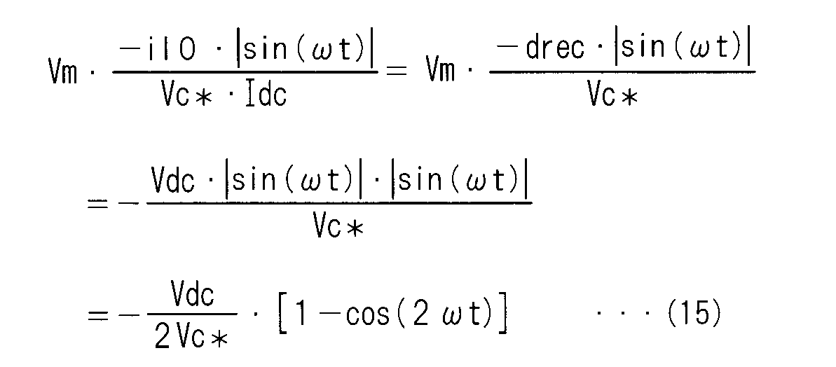
- the second aspect of the control device outputs a discharge switch signal (SSc) for conducting the first switch based on the discharge duty (dc ′), and the discharge duty is a voltage across the capacitor (Vc). , Vc *) and a product of a third ratio (Vdc / Vc) of the predetermined voltage (Vdc) and a cosine value (cos (2 ⁇ t)) that is twice the phase ( ⁇ t) of the AC voltage, and the both ends. Based on the product of the fourth ratio (Vm / Vc) of the amplitude (Vm) to the voltage, the second ratio (il / Idc), and the absolute value (
- the third current is the fourth current (il).
- the third aspect of the control device outputs a discharge switch signal (SSc) for conducting the first switch based on the discharge duty (dc ′′), and the discharge duty is a voltage across the capacitor ( Product of the third ratio (Vdc / Vc) of the predetermined voltage (Vdc) with respect to Vc, Vc *) and the square of the cosine value of the phase ( ⁇ t) of the AC voltage (cos 2 ( ⁇ t)), and the both-ends voltage Is set based on the product of the fourth ratio (Vm / Vc), the second ratio (il ′ / Idc), and the absolute value (
- the third current is the reduction amount (il ′) of the harmonic component of the fourth current (il).
- control device (10) further includes a correction amount generation unit (1025) that obtains the reduction amount (il ′) based on the harmonic component of the input current (Iin) input to the converter (3).
- control device (10) further includes a correction amount generator (1026) that obtains the reduction amount (il ′) based on the harmonic component of the fourth current (il).
- the duty generation unit includes an original rectification duty (drec) that is a product of the first ratio (Vdc / Vm) and the absolute value (
- a fourth aspect of the control device for a direct power converter according to the present invention is the second aspect or the third aspect thereof.
- the charging circuit (4b) includes the capacitor ( A diode (D40) including a cathode connected to C4) and an anode; a reactor (L4) connected between the first DC power supply line (LH; LH1, LH2) and the anode; And a second switch (S1, D41) connected between the two DC power supply lines (LL) and the anode.
- the third aspect of the control device includes a switch control signal generator (SS1) that generates a control signal (SSl) that causes the second switch to turn on and off once in one cycle of the rectified voltage (Vrec). 1031).
- the distortion of the waveform of the input current with respect to the sine wave is reduced regardless of the waveform of the third current.
- the power output from the inverter is smoothed regardless of the waveform of the third current.
- noise generated by the second switch is reduced.
- the block diagram which shows the structure of the direct power converter which can apply the control technique concerning this invention The block diagram which illustrates the composition of a control device.
- movement of a direct form power converter The graph which shows the waveform of a buffer current when adopting simple switching.
- movement of a direct form power converter The graph which shows operation
- movement of a direct form power converter The graph which shows operation
- movement of a direct form power converter The graph which shows operation
- movement of a direct form power converter The graph which shows the waveform in the half cycle of a single phase alternating voltage of a reactor current.
- FIG. 1 is a block diagram showing a configuration of a direct power converter to which a control technique according to the present invention can be applied.
- the direct power converter includes a converter 3, a power buffer circuit 4, an inverter 5, and a DC link 7.
- the power buffer circuit 4 functions as the above-described active buffer.
- the converter 3 is connected to the single-phase AC power source 1 through the filter 2, for example.
- the filter 2 includes a reactor L2 and a capacitor C2.
- Reactor L ⁇ b> 2 is provided between one of the two output ends of single-phase AC power supply 1 and converter 3.
- the capacitor C2 is provided between the two output terminals of the single-phase AC power source 1.
- the filter 2 removes high-frequency components mainly derived from the switching operation of the inverter 5 from the current.
- the filter 2 may be omitted. Alternatively, it may be provided between the converter 3 and the power buffer circuit 4.
- the position of the filter 2 will be described later in the second modification. For the sake of simplicity, the following description will be made ignoring the function of the filter 2.
- DC link 7 has DC power supply lines LH and LL.
- the converter 3 employs a diode bridge, for example, and includes diodes D31 to D34.
- ; Vin Vm ⁇ sin ( ⁇ t)), which is output between the DC power supply lines LH and LL.
- a higher potential than the DC power supply line LL is applied to the DC power supply line LH.
- ; Iin Im ⁇ sin ( ⁇ t)).
- the power buffer circuit 4 includes a discharge circuit 4a, a charging circuit 4b, and a current blocking circuit 4c, and exchanges power with the DC link 7.
- the discharge circuit 4a includes a capacitor C4 as a buffer capacitor, and the charging circuit 4b boosts the rectified voltage Vrec to charge the capacitor C4.
- the current blocking circuit 4c blocks current flowing from the discharging circuit 4a to the charging circuit 4b.
- the discharge circuit 4a further includes a diode D42 and a transistor (herein, insulated gate bipolar transistor: hereinafter abbreviated as “IGBT”) Sc connected in antiparallel with the diode D42.
- the transistor Sc is connected in series between the DC power supply lines LH and LL on the DC power supply line LH side with respect to the capacitor C4.
- reverse parallel connection means that the forward directions are opposite to each other and connected in parallel.
- the forward direction of the transistor Sc is a direction from the DC power supply line LL to the DC power supply line LH
- the forward direction of the diode D42 is a direction from the DC power supply line LH to the DC power supply line LL.
- the transistor Sc and the diode D42 can be collectively understood as one switch element (switch Sc).
- Capacitor C4 is discharged by conduction of switch Sc, and power is given to DC link 7.
- the charging circuit 4b includes, for example, a diode D40, a reactor L4, and a transistor (IGBT here) Sl.
- the diode D40 includes a cathode and an anode, and the cathode is connected between the switch Sc and the capacitor C4.
- Such a configuration is known as a so-called boost chopper.
- Reactor L4 is connected between DC power supply line LH and the anode of diode D40.
- Transistor S1 is connected between DC power supply line LL and the anode of diode D40.
- a diode D41 is connected in reverse parallel to the transistor Sl, and both of them can be grasped as one switch element (switch Sl). Specifically, the forward direction of the transistor S1 is a direction from the DC power supply line LH to the DC power supply line LL, and the forward direction of the diode D41 is a direction from the DC power supply line LL to the DC power supply line LH.
- the capacitor C4 is charged by the charging circuit 4b, and a both-end voltage Vc higher than the rectified voltage Vrec is generated. Specifically, energy is accumulated in the reactor L4 by flowing a current from the DC power supply line LH to the DC power supply line LL via the switch Sl, and then the energy passes through the diode D40 by turning off the switch Sl. And stored in the capacitor C4.
- the diode D42 secures a reverse breakdown voltage when the voltage Vc at both ends is lower than the rectified voltage Vrec, and reversely conducts a current flowing back from the inductive load 6 to the DC link 7 when the inverter 5 is abnormally stopped.
- the diode D41 is a diode for causing reverse breakdown voltage and reverse conduction, and is exemplified as a diode built in the transistor S1 realized by the IGBT, but the diode D41 itself is not involved in the circuit operation.
- the current blocking circuit 4c is provided on the DC power supply line LH between the charging circuit 4b and the discharging circuit 4a, and is realized by a diode D43, for example.
- the anode of the diode D43 is connected to the reactor L4 on the side opposite to the switch Sl (that is, on the converter 3 side).
- the cathode of the diode D43 is connected to the switch Sc on the side opposite to the capacitor C4 (that is, on the inverter 5 side).
- Such a current blocking circuit 4c is known from Patent Document 5, for example.
- the inverter 5 converts the DC voltage between the DC power supply lines LH and LL into an AC voltage and outputs it to the output terminals Pu, Pv and Pw.
- the inverter 5 includes six switching elements Sup, Svp, Swp, Sun, Svn, and Swn.
- the switching elements Sup, Svp, Swp are respectively connected between the output terminals Pu, Pv, Pw and the DC power supply line LH, and the switching elements Sun, Svn, Swn are respectively connected to the output terminals Pu, Pv, Pw and the DC power supply line LL. Connected between.
- the inverter 5 constitutes a so-called voltage source inverter and includes six diodes Dup, Dvp, Dwp, Dun, Dvn, Dwn.
- the diodes Dup, Dvp, Dwp, Dun, Dvn, and Dwn are all arranged with the cathode facing the DC power supply line LH and the anode facing the DC power supply line LL.
- the diode Dup is connected in parallel with the switching element Sup between the output terminal Pu and the DC power supply line LH.
- the diodes Dvp, Dwp, Dun, Dvn, Dwn are connected in parallel with the switching elements Svp, Swp, Sun, Svn, Swn, respectively.
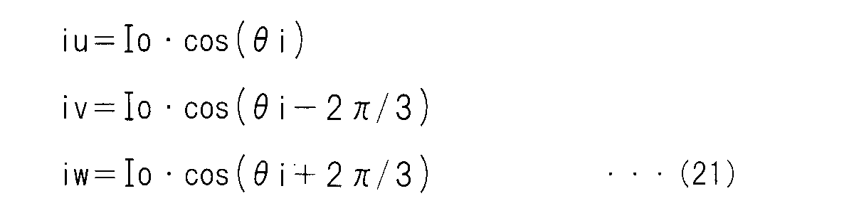
- Load currents iu, iv, and iw are output from the output terminals Pu, Pv, and Pw, respectively, and constitute a three-phase alternating current.
- IGBTs are employed for the switching elements Sup, Svp, Swp, Sun, Svn, and Swn.
- the inductive load 6 is a rotating machine, for example, and is illustrated by an equivalent circuit indicating that it is an inductive load.
- the reactor Lu and the resistor Ru are connected in series with each other, and one end of this series structure is connected to the output end Pu.
- a similar series structure is obtained for reactors Lv, Lw and resistors Rv, Rw. The other ends of these series structures are connected to each other.
- the speed detection unit 9 detects the load currents iu, iv, iw flowing through the inductive load 6, and the rotational angular speed ⁇ m and the q-axis current Iq obtained from them.
- the d-axis current Id (to be precise, information indicating them; the same applies hereinafter) is supplied to the control device 10 for the direct power converter.
- the current Ish is an instantaneous value of the current flowing through the inverter 5, and is measured by a well-known technique in one of the DC power supply lines LL and LH.
- the current il is a reactor current that flows through the reactor L4 and corresponds to the buffer current described above.
- the reactor current il is measured by, for example, a known current protection device. Since the configuration for obtaining the currents Ish and il is a well-known technique, the illustration is omitted.
- FIG. 2 is a block diagram illustrating the configuration of the control device 10.
- the control device 10 includes an inverter control unit 101, a discharge control unit 102, and a charge control unit 103.
- the inverter control unit 101 outputs a discharge duty dc ′, a rectification duty drec ′, and a command value of voltage output from the inverter 5 (hereinafter referred to as “voltage command”) described in “B.
- the inverter control signals SSup, SSvp, SSwp, SSun, SSvn, SSwn are output based on Vu *, Vv *, Vw *.
- the inverter control signals SSup, SSvp, SSwp, SSun, SSvn, and SSwn control the operation of the switching elements Sup, Svp, Swp, Sun, Svn, and Swn, respectively.
- the inverter control unit 101 further includes an amplitude modulation command unit 1012, a product-sum operation unit 1013, a comparison unit 1014, and a logic operation unit 1015.
- the amplitude modulation command unit 1012 controls the operation of the product-sum calculation unit 1013 based on the discharge duty dc 'and the rectification duty drec'.
- the product-sum operation unit 1013 (represented by a symbol only for the multiplier for the sake of simplicity) calculates the product-sum operation of the voltage command values Vu *, Vv *, Vw * and the discharge duty dc ′ and the rectification duty drec ′. To generate a signal wave M.
- the comparison unit 1014 outputs the comparison result of the values of the signal wave M and the carrier CA to the logic operation unit 1015.
- the logic operation unit 1015 performs a logic operation on the comparison result, and outputs inverter control signals SSup, SSvp, SSwp, SSun, SSvn, SSwn.
- the discharge controller 102 includes a duty calculator 1021, a comparator 1022, and a duty corrector 1023.
- the duty calculator 1021 receives the phase ⁇ , the amplitude Vm, the command value Vc * of the both-ends voltage Vc, and the command value Vdc * of the DC voltage Vdc described later, and obtains the original discharge duty dc and the original rectification duty drec.
- the duty correction unit 1023 corrects the original discharge duty dc and the original rectification duty drec to obtain the discharge duty dc ′ and the rectification duty drec ′, respectively.
- the duty calculation unit 1021 and the duty correction unit 1023 can be collectively understood as a duty generation unit that generates the discharge duty dc ′ and the rectification duty drec ′.
- the comparator 1022 compares the discharge duty dc 'with the carrier CA, and generates a discharge switch signal SSc for conducting the switch Sc.
- the charging control unit 103 includes a switch control signal generation unit 1031 that generates a control signal SS1 for controlling on / off of the switch Sl. Since the switch control signal generation unit 1031 is known from Non-Patent Documents 4 and 5, the details thereof will be omitted, but will be briefly described later. For example, the switch control signal generation unit 1031 generates the control signal SSl based on the output power Pout that is the instantaneous power output from the inverter 5 and the amplitude Vm.
- Converter input power Pin has an AC component ( ⁇ 1/2) ⁇ Vm ⁇ Im ⁇ cos (2 ⁇ t) indicated by the second term on the rightmost side of equation (1) (hereinafter also referred to as “AC component Pin ⁇ ”). ). Therefore, hereinafter, the converter input power Pin may be referred to as pulsating power Pin.
- the power converter shown in FIG. 1 can be grasped as follows.
- the converter 3 receives a single-phase AC voltage Vin and outputs a pulsating power Pin:
- the power buffer circuit 4 inputs the instantaneous power P1 (hereinafter also referred to as “accepted power P1”) from the DC link 7 and outputs the instantaneous power Pc (hereinafter also referred to as “provided power Pc”) to the DC link 7:
- FIG. 3 is a block diagram schematically showing the power balance in the direct power converter shown in FIG.
- the buffered instantaneous power Pbuf (hereinafter also referred to as “buffering power Pbuf”) is equal to the power difference (Pc ⁇ Pl) obtained by subtracting the received power Pl from the given power Pc.
- FIG. 4 is shown as an equivalent circuit of the direct power converter shown in FIG.
- the equivalent circuit is introduced in Patent Documents 1 and 2, for example.
- the current irec1 is equivalently represented as a current irec1 passing through the switch Srec when it is turned on.
- the discharge current ic is equivalently expressed as a current ic passing through the switch Sc when it is conductive.
- the switch Sz also conducts current that flows to the inductive load 6 via the inverter 5. Is equivalently expressed as a zero-phase current iz that flows through this.
- FIG. 4 the reactor L4, the diode D40, and the switch Sl constituting the charging circuit 4b are shown, and the reactor current il flowing through the reactor L4 is appended.
- the duty drec ' is a duty that sets a period in which the converter 3 is connected to the DC link 7 and a current can flow to the inverter 5, it indicates the above-described rectification duty drec'.
- the duty dz ′ is a duty through which the zero-phase current iz always flows regardless of the voltage output from the inverter 5, it may be referred to as a zero duty dz ′.
- the direct current Idc is a current that flows to the inductive load 6 via the inverter 5 and can be obtained from the current Ish as described later.
- the currents irec1, ic, and iz are obtained by multiplying the direct current Idc by the duties drec ', dc', and dz ', respectively. Therefore, these are average values in the switching period of the switches Srec, Sc, Sz.
- the duties drec ', dc', and dz ' can also be regarded as the current distribution ratio of the direct current Idc with respect to the currents irec1, ic, and iz.
- the current irec1 can be obtained by switching the inverter 5 and the switch Sc according to the zero duty dz 'and the discharge duty dc'.
- the inverter 5 cannot use the DC voltage in the DC link 7 during the period in which the zero-phase current iz flows. Therefore, the DC voltage used for power supply to the inverter 5 in the DC link 7 has a meaning in power conversion. In other words, an instantaneous DC voltage that the inverter 5 does not use for power conversion has no meaning.
- the direct current Idc can be expressed by the following expression (3) in consideration of the expression (2) by introducing a DC voltage Vdc which has meaning in power conversion.
- the DC voltage Vdc can be expressed by the following equation (4).
- the DC voltage Vdc can be grasped as a voltage applied to the DC link 7 as an average value of the maximum value of the voltage that can be output from the inverter 5 with respect to the cycle for controlling the switching of the switches Sc and Sl and the inverter 5. it can.
- the inverter 5 can contribute to the voltage of the DC link 7 at a ratio of zero duty dz ′, the inverter 5 is insulated from one of the DC power supply lines LL and LH during the period corresponding to the zero duty dz ′. It is.
- the DC voltage Vdc is added as a voltage generated at both ends of a current source Idc (which flows the DC current Idc) representing the inverter 5 and the inductive load 6 in FIG.
- the inverter input power Pdc can be obtained as follows.
- control for realizing the expressions (3) and (4) can be performed by controlling the pulsation (AC component) of the expression (6) to zero.
- FIG. 5 An example of a configuration for performing the above control is shown in FIG. 5 as a block diagram. This configuration is provided, for example, in the configuration shown as the output voltage command generation unit 1011 in FIG.
- the inductive load 6 is a rotating machine
- its rotating angular velocity ⁇ m, field magnetic flux ⁇ a of the rotating machine d-axis inductance Ld and q-axis inductance Lq of the rotating machine
- q-axis current command values Iq * and d A q-axis voltage command value Vq * and a d-axis voltage command value Vd * are obtained based on the shaft current command value Id *, the q-axis current Iq, and the d-axis current Id.
- Voltage command values Vu *, Vv *, and Vw * for controlling the inverter 5 are generated from the q-axis voltage command value Vq * and the d-axis voltage command value Vd *.
- the speed detector 9 detects the load currents iu, iv, iw flowing through the inductive load 6, and the rotational angular speed ⁇ m, q-axis current Iq, and d-axis current Id obtained from these are detected. This is given to the control device 10.
- the DC power calculation unit 711 receives the q-axis voltage command value Vq * and the d-axis voltage command value Vd *, the q-axis current Iq and the d-axis current Id, and inputs the inverter input power based on the above equation (6).
- Pdc is calculated and given to the pulsation extraction unit 712.
- the pulsation extraction unit 712 extracts and outputs the alternating current component of Expression (6).
- the pulsation extraction unit 712 is realized by, for example, a high-pass (high-pass transmission) filter HPF.
- HPF high-pass transmission filter
- the subtractor 715 performs a process of correcting the current command value Ia * in the normal process with the output of the PI processing unit 716. Specifically, first, as a normal process for obtaining the current command value Ia *, a subtractor 701 obtains a deviation between the rotational angular velocity ⁇ m and the command value ⁇ m *. The deviation is subjected to proportional-integral control in the PI processing unit 702, and the current command value Ia * is obtained once. Then, the subtractor 715 performs processing for reducing the current command value Ia * by the output from the PI processing unit 716.
- the above-described known technique is applied to the current command value Ia * corrected by the processing unit 71 in this way to generate the q-axis voltage command value Vq * and the d-axis voltage command value Vd *.
- control is performed with feedback on the q-axis voltage command value Vq * and the d-axis voltage command value Vd *, the q-axis current Iq, and the d-axis current Id, and the inverter input power Pdc is AC.
- the component is converged to 0.
- the commutation duty drec ′ and the discharge duty dc ′ are determined without particularly setting the distinction between the acceptance period and the grant period.
- the original rectification duty drec and the original discharge duty dc are defined by equations (7) and (8), respectively.
- the command value Vdc * can be adopted as the DC voltage Vdc. That is, hereinafter, the DC voltage Vdc is treated as a predetermined voltage.
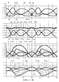
- the dutys drec, dc, and dz are shown at the top, the DC voltage Vdc and the voltages drec ⁇ Vrec, dc ⁇ Vc (see equation (4)) and the DC current Idc that constitute this are shown at the second level from the top, Currents irec, ic, il and irec1 are shown in the third stage from the top, and instantaneous powers Pin, Pdc, Pbuf, Pc, -Pl and Prec are shown in the bottom stage. It is assumed that the voltage Vc at both ends accurately follows the command value Vc *.
- the horizontal axis indicates the phase ⁇ t in units of “degrees”.
- the currents Idc, irec, ic, il, and irec1 were converted with the amplitude Im as ⁇ 2.
- the instantaneous powers Pin, Pout, Pbuf, Pc, -Pl, Prec are obtained as the product of the voltage converted as described above and the current.
- FIG. 6 illustrates the case where the reactor current il takes the value il0, and the waveform of the current irec exhibits an absolute value of a sine wave.
- the direct power converter is controlled using the rectification duty drec 'obtained by correcting the original rectification duty drec as follows.
- the direct power converter is controlled using the discharge duty dc 'obtained by correcting the original discharge duty dc as follows.
- the following equation (18) is obtained from the equations (16) and (17), and the second term enclosed in square brackets (symbol “[” and symbol “]”) on the right side is a correction term for the original discharge duty dc.
- the correction term is a value obtained by adding the first value to the original discharge duty dc.
- the first value is a value obtained by dividing the second value by the command value Vc *, and the second value is a ratio (il / Idc) is a value obtained by subtracting the DC voltage Vdc from the product of the rectified voltage Vrec.
- the output power Pout is smoothed and the pulsation is removed regardless of the waveform of the reactor current il.
- the corrections shown in the expressions (13) and (18) are performed based on the ratio (il / Idc). Moreover, the amplitude Im of the input current is not necessary not only for generating the original rectification duty drec and the original discharge duty dc, but also for correcting for obtaining the rectification duty drec 'and the discharge duty dc'.
- Period T0 is one period of carrier CA.
- Periods ⁇ 4 and ⁇ 6 indicate the lengths of periods in which the first state and the second state are realized in the period T0, respectively.
- the first state and the second state will be described by focusing on the period in which the switching element Swp is kept off and the switching element Swn is kept on in the inverter 5 in one period of the carrier CA.
- the first state is a state in which the switching elements Sup and Svn are turned on and the switching elements Sun and Svp are turned off.
- the second state is a state in which the switching elements Sup and Svp are turned on and the switching elements Sun and Svn are turned off. It is known that Expression (20) is established by introducing a phase ⁇ v of the voltage output from the inverter 5 and a coefficient of 0 ⁇ k ⁇ 1 (see, for example, Patent Document 4).
- the load currents iu, iv and iw are three-phase alternating current, and the equation (21) is established.
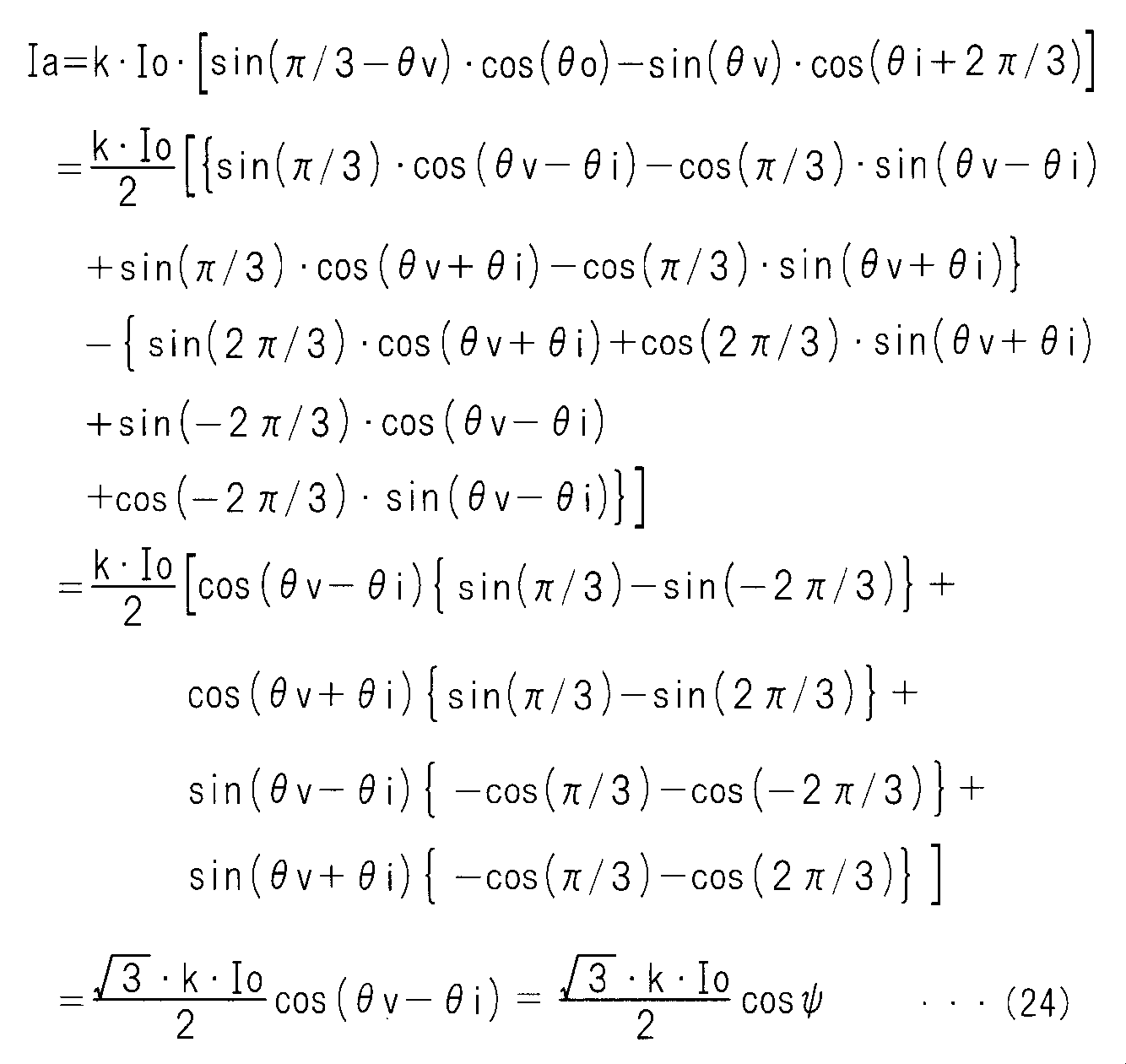
- the direct current Idc the current Ia shown in the equation (22) is used.
- the period T0 is one period of the carrier CA, and the periods ⁇ 4 and ⁇ 6 indicate the lengths of the periods in which the first state and the second state are realized in the period T0, respectively.
- currents Ish (t4) and Ish (t6) indicate the values of the current Ish measured at times t4 and t6, respectively. Times t4 and t6 are selected from the time points when the first state and the second state are realized, respectively.
- the load current iu flows from the output terminal Pu to the inductive load 6 and flows from the output terminals Pv and Pw to the DC power supply line LL.
- Expression (22) is transformed into Expression (24) below.
- ⁇ ⁇ v ⁇ i is a phase difference between the voltage and current output from the inverter 5
- cos ⁇ indicates the power factor of the inverter 5.
- Formula (25) will be materialized.
- the voltage Vr and the current ir are the effective values of the voltage and current output from the inverter 5, respectively.
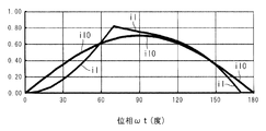
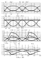
- Example of reactor current il As described above, even when the waveform of the reactor current il does not exhibit the absolute value of a sine wave, power buffering can be performed while making the input current Iin a sine wave. Therefore, in the following, the operation of the present embodiment will be described taking the reactor current il when simple switching is employed as an example. By causing the reactor current il to flow by simple switching, the generation of noise generated by the switch Sl is reduced, and by reducing distortion from the sine wave of the input current Iin, the power supply harmonics can be reduced.
- FIG. 7 is a graph showing the waveform of the reactor current il when simple switching is employed.
- an area of 0 to 180 degrees is shown as the phase ⁇ t.
- the waveform of the value il0 is also shown.
- Non-Patent Document 5 shows the relationship among the value Ts, the voltage Vc at both ends, the power factor, and the output power corresponding to the period during which the switch Sl is turned on in FIG.
- the inductance of the reactor L4 is 1H
- Vm 1V
- Vc 1.14V
- 45 mW is adopted as the power that maximizes the power factor.
- Ts 0.194.
- This is ⁇ 70 (degrees) in terms of phase. Therefore, in the graph shown in FIG. 7, the reactor current il increases when the phase ⁇ t is 0 to 70 degrees.
- the reactor current il decreases when the phase ⁇ t is 70 to 180 degrees, and when it reaches the value 0, the value 0 is maintained even if the phase ⁇ t advances.
- the phase at which the reactor current il decreases to reach the value 0 is about 170 degrees.
- Non-Patent Document 4 a more specific waveform of the reactor current il is calculated.
- il Ip ⁇ (1 ⁇ cos ( ⁇ t))
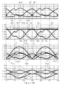
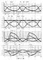
- the dutys drec ′, dc ′, and dz ′ are at the uppermost stage, the DC voltage Vdc is at the second stage from the top, and the voltages drec ′, Vrec, dc ′, and Vc that form the DC voltage Vdc (see Expression (19))
- the direct current Idc, the currents irec, ic, il, and irec1 in the third stage from the top and the instantaneous powers Pin, Pdc, Pbuf, Pc, -Pl, and Prec in the bottom stage, respectively.
- the control using the rectification duty drec ′ and the discharge duty dc ′ is performed, so that not only the inverter input power Pdc but also the DC voltage Vdc and the DC current are controlled.
- Idc is constant and the waveform of the current irec is an absolute value of a sine wave. This shows that the waveform of the input current Iin is a sine wave.
- the power buffer circuit 4 functions as a power buffer.
- the zero duty can be made non-negative by another method.
- the waveform shown in FIG. 7 was adopted as the reactor current il.
- FIG. 10 also shows various amounts as in FIG.
- the amplitude Im is set to ⁇ 2 and the amplitude Vm is set to 1, respectively.
- Vc 1.14 Vm
- Non-Patent Document 5 exemplifies a case where a DC voltage of 270 V is obtained by voltage doubler rectification from a 100 V power supply (single phase, effective voltage value 100 V).
- Vc 270/2 / (100 ⁇ ⁇ 2) ⁇ 0.95.
- the power that maximizes the power factor is about 30 mW.
- the inductance value is listed as 6.2 mH.
- the power is 45/30 times.
- Vm 230V. Therefore, compared with the double voltage rectification employed in Non-Patent Document 5, the effect of full wave rectification employed in the present embodiment on the inductance is (230/100) 2 times. Therefore, the required inductance value is 6.5 [mH] ⁇ 45/30 ⁇ (230/100) 2 ⁇ 52 [mH].
- Non-Patent Document 4 introduces a technique for delaying the start time of conduction of a switching element. According to such a technique, a high power factor can be obtained even with a small inductance.
- the inductance L has a value that maximizes the power factor.
- Data in which the power factor has the maximum value in each of the graphs G0, G1, G2, and G3 is plotted as white.
- the power factor becomes maximum when the inductance L is 51.37 mH.
- the reactor L4 is set to have an inductance of 15 mH to 30 mH. It is desirable to be adopted.
- the conduction start phase is desirably 45 degrees (see graph G3) from the viewpoint of flat power factor characteristics.
- the conduction start phase is 36 degrees (see graph G2). In the following description, 36 degrees is used for the conduction start phase.
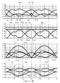
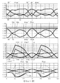
- FIG. 12 also shows various amounts as in FIG. Specifically, the dutys drec ′, dc ′, dz ′ are shown at the top, the DC voltage Vdc and the voltages drec ′ / Vrec, dc ′ / Vc and the DC current Idc constituting the DC voltage Vdc are shown at the top from the top.
- the currents irec, ic, il, and irec1 are shown in the third stage, and the instantaneous powers Pin, Pdc, Pbuf, Pc, -Pl, and Prec are shown in the bottom stage.
- FIG. 13 shows various amounts as in FIG.
- the minimum value of the DC voltage Vdc is 0.72 Vm in FIG. 13 and is lower than the minimum value 0.80 Vm in FIG.
- Such a decrease in the minimum value of the DC voltage Vdc that fluctuates and a decrease in the maximum value of the DC voltage Vdc that can be made constant reduce the period in which the reactor current il flows due to the decrease in the inductance L, and the reactor current il has harmonics. This is considered to be derived from the fact that many components (specifically, odd-order components of the third or higher order of the frequency of the single-phase AC voltage Vin) are included.
- FIG. 15 is a graph showing a waveform of the reactor current il exemplified in FIGS. 12 to 14 for a half cycle of the single-phase AC voltage Vin, specifically, when the phase ⁇ t is 0 to 180 degrees. Even when the phase ⁇ t is 180 to 360 degrees, the reactor current il shows the same waveform. As described above, 1.84 kW of electric power (effective voltage value 230 V, effective current value 8 A) was adopted, and the inductance L was 28.54 mH. The reactor current il is shown with an amplitude Im of ⁇ 2.
- the standard IEC61000-3-2 allows third harmonic components up to an effective value of 2.30A under the condition of a rated voltage of 230V.
- FIG. 16 is a graph showing the waveform of the input current Iin when the correction amount is subtracted from the reactor current il as described above.
- Vc 1.14 Vm was set
- the amplitude Vm was set to 1
- the amplitude Im of the input current Iin before subtracting the correction amount was set to ⁇ 2.
- the harmonics of the input current lin fall within the allowable range of the standard IEC61000-3-2.
- the rectification duty drec ′′, the discharge duty dc ′′, and the zero duty dz ′′ are set as follows.
- a correction amount il ′ for the reactor current il is introduced.
- the correction amount il ′ is the reduction amount (0.571 A) of the third harmonic component of the reactor current il.
- the deviation amount (il-i0) from the value il0 of the reactor current il is used. Therefore, in order to obtain the rectification duty drec ′′ from the original rectification duty drec by subtracting the correction amount il ′, the rectification duty drec ′ is formally changed to the rectification duty drec ′′ in the equation (12), and the deviation amount (il ⁇ i0 ) May be replaced with the value ( ⁇ il ′). Further, considering equation (7), equation (27) is obtained.
- formula (28) is obtained by replacing the discharge duty dc ′ with the discharge duty dc ′′ and the deviation (il ⁇ i0) with the value ( ⁇ il ′). . Further, considering equation (8), equation (29) is obtained.
- Equation (19) Equation (30) is obtained. That is, it can be understood that the DC voltage Vdc can be controlled to be constant by employing the rectification duty drec "and the discharge duty dc".
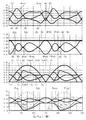
- FIG. 17 aligns the description using FIG. 12 with the values of the specifications, sets the rectification duty drec ′′ and the discharge duty dc ′′ by the equations (27) and (29), respectively, and sets the zero duty dz ′′ to 1.
- 10 is a graph showing various quantities when set with ⁇ drec ′′ ⁇ dc ′′. It can be seen that there is a phase region where dz ′′ ⁇ 0.
- FIG. 18 shows the description using FIG. 13 and the values of specifications, and sets the rectification duty drec ′′ and the discharge duty dc ′′ by the equations (27) and (29), respectively, and sets the zero duty dz ′′ to 1.
- FIG. 19 is a graph showing various amounts when the rectification duty drec ′′, the discharge duty dc ′′, and the zero duty dz ′′ are set in the same manner as FIG.
- Vdc 0.82 Vm
- the inductance L is reduced to reduce the size of the reactor L4, and by suppressing the harmonic component of the reactor current il associated therewith, the harmonics of the input current Iin are reduced and the waveform of the input current Iin is reduced.
- the DC voltage Vdc that the inverter 5 can use for power conversion is increased while allowing distortion from the sine wave.
- FIG. 20 is a graph showing a waveform of the reactor current il in a half cycle of the single-phase AC voltage Vin, and more specifically, a graph showing a waveform when the phase ⁇ t is 0 to 180 degrees. Even when the phase ⁇ t is 180 to 360 degrees, the reactor current il shows the same waveform.
- the phase at which the switch Sl shifts from conduction to non-conduction is about 61 (360 ⁇ 0.17) degrees.
- the reactor current il takes a maximum value, and is about 141 The reactor current il becomes 0 at (360 ⁇ 0.394) degrees.
- the third harmonic component, the seventh harmonic component, and the eleventh harmonic component are effective values 2.30 A, 0.77 A, and 0, respectively. Allow up to 33A.
- the reactor current il shown in FIG. 20 has a third harmonic component having an effective value of 3.66A, a seventh harmonic component having an effective value of 1.17A, and an effective value of 0.2 when the voltage effective value is 230V.
- Each of the harmonic components of the other orders is within the allowable range of the standard IEC61000-3-2.
- FIG. 21 is a graph showing the waveform of the input current Iin when the correction amount il ′ is subtracted from the reactor current il as described above.
- Vc 1.14 Vm was set
- the amplitude Vm was set to 1
- the amplitude Im of the input current Iin before subtraction of the correction amount il ′ was set to ⁇ 2.
- the harmonic component of the input current lin falls within the allowable range of the standard IEC61000-3-2.
- FIG. 22 shows the description using FIG. 18 and the values of specifications other than the inductance L, and sets the rectification duty drec ′′ and the discharge duty dc ′′ by the equations (27) and (29), respectively.
- the minimum value of the zero duty dz ′′ can be set to 0 instead of a positive value. That is, if the rectification duty drec ′′, the discharge duty dc ′′, and the zero duty dz ′′ are employed, even if the inductance L is as small as 18 mH, the inductance L is about 51 mH, the rectification duty drec ′, and the discharge duty dc.
- the harmonic component of the input current Iin can be within the allowable range of the standard.
- the commutation duty (drec ', drec'') is The product of the ratio Vdc / Vm of the DC voltage Vdc to the amplitude Vm and the absolute value
- the above product indicates the original rectification duty drec (see equation (7)).
- the above “current” is the reactor current il for the rectification duty drec ′ and the correction amount il ′ for the rectification duty drec ′′.
- the correction amount il ′ is a reduction amount of the higher order harmonic component to be reduced.
- the rectification duty drec ′ takes a value obtained by subtracting the ratio il / Idc from twice the product (Vdc / Vm) ⁇
- the rectification duty drec ′′ is a value obtained by adding the ratio il ′ / Idc to the product (Vdc / Vm) ⁇
- the discharge duty dc ′ can be expressed as follows based on equation (16): The product of the ratio Vdc / Vc of the DC voltage Vdc to the voltage Vc across the capacitor C4 (which accurately follows the command value Vc *) and the cosine value cos (2 ⁇ t) that is twice the phase ⁇ t (Vdc / Vc) ⁇ cos (2 ⁇ t); and the product (Vm / Vc) ⁇ (il / Idc) of the ratio Vm / Vc of the amplitude Vm to the both-ends voltage Vc, the ratio il / Idc, and the absolute value
- the discharge duty dc ′′ can be expressed as follows based on equation (29): A first product (Vdc) of the ratio Vdc / Vc of the DC voltage Vdc to the voltage Vc across the capacitor C4 (which accurately follows the command value Vc *) and the square cosine 2 of the cosine value of the phase ⁇ t ( ⁇ t).
- the value of the discharge duty dc ′′ is a value obtained by subtracting the second product from the first product.
- the first product indicates the original discharge duty (see equation (8)).
- FIG. 24 is a block diagram illustrating a first configuration of the discharge control unit 102 for obtaining the rectification duty drec ′′ and the discharge duty dc ′′ and the vicinity thereof.
- the discharge control unit 102 also constitutes the control device 10 together with the inverter control unit 101 and the charge control unit 103 shown in FIG.
- the discharge control unit 102 includes a correction amount generation unit 1025 in addition to the duty calculation unit 1021, the comparator 1022, the duty correction unit 1023, and the link current calculation unit 1024 described with reference to FIG.
- the duty correction unit 1023 obtains the rectification duty drec ′′ and the discharge duty dc ′′ from the original rectification duty drec and the original discharge duty dc, respectively, according to the equations (27) and (29) (particularly the first equations). .
- FIG. 25 is a block diagram illustrating the configuration of the correction amount generation unit 1025.
- the correction amount generation unit 1025 includes an input current estimation unit 1025a and a correction harmonic table 1025b.
- the input current estimation unit 1025a obtains an estimated value Is of the input current Iin based on the output power Pout, the amplitude Vm, and the phase ⁇ t. For example, the following formula can be adopted.
- the correction harmonic table 1025b stores a table indicating the relationship between the input current Iin and the regulated amount of the harmonic component, searches the table using the estimated value Is as the input current Iin, and corresponding correction amount il ′. Is output.
- the correction amount il ′ is obtained based on the distortion of the input current Iin. Therefore, in the first configuration, the reactor 10 does not require the reactor current il.
- FIG. 26 is a block diagram illustrating a second configuration of the discharge control unit 102 for obtaining the rectification duty drec ′′ and the discharge duty dc ′′ and the vicinity thereof.
- the discharge control unit 102 also constitutes the control device 10 together with the inverter control unit 101 and the charge control unit 103 shown in FIG.
- the discharge control unit 102 includes a correction amount generation unit 1026 in addition to the duty calculation unit 1021, the comparator 1022, the duty correction unit 1023, and the link current calculation unit 1024 described with reference to FIG.
- the duty correction unit 1023 obtains the rectification duty drec ′′ and the discharge duty dc ′′ according to the equations (27) and (29) (particularly the first equations of the respective equations).
- FIG. 27 is a block diagram illustrating the configuration of the correction amount generation unit 1026.
- the correction amount generation unit 1026 includes an FFT calculation unit 1026a, a correction harmonic selection unit 1026b, and an inverse FFT calculation unit 1026c.
- the FFT operation unit 1026a performs a fast Fourier transform on the reactor current il to obtain an amplitude Ilh (n) for each component of the nth order frequency.
- the corrected harmonic selection unit 1026b selects a harmonic order that exceeds the upper limit set for each order.
- the ⁇ -order harmonic correction amount Il is the amount by which the amplitude Ilh ( ⁇ ) of the ⁇ -order harmonic component exceeds the upper limit set for the ⁇ -order harmonic.
- the correction amount Il ′ ( ⁇ ) ( ⁇ ⁇ ⁇ ) of the order not selected is set to 0.
- the inverse FFT operation unit 1026c performs an inverse fast Fourier transform using the correction amount Il ′ (n) or the correction amount Il ′ ( ⁇ ) to obtain the correction amount il ′.
- the correction amount il ′ is obtained based on the distortion of the reactor current il (see FIGS. 15 and 20).
- FIG. 28 is a circuit diagram showing only the vicinity when the converter 3 is replaced with diode bridges 3a and 3b as a first modification of the power converter. Such a configuration itself is known from Non-Patent Document 1, for example.
- the diode bridge 3a has diodes D31, D32, D33, and D34 as in the converter 3 described in the above embodiment, and these constitute a bridge circuit.
- the diode bridge 3b includes diodes D35, D36, D32, and D34, which constitute a bridge circuit. That is, the diode bridges 3a and 3b share the diodes D32 and D34.
- the DC power supply line LH shown in the above embodiment is replaced with two DC power supply lines LH1 and LH2.
- the DC power supply line LL is connected to the anodes of the diodes D32 and D34, the switch S1 on the side opposite to the reactor L4, the capacitor C4 on the side opposite to the switch Sc, and the inverter 5 as in the above embodiment. Each is connected.
- the DC power supply line LH1 is connected to the switch Sc and the inverter 5 on the opposite side of the capacitor C4, with the cathodes of the diodes D31 and D33 connected in common as in the DC power supply line LH.
- the cathodes of the diodes D35 and D36 are connected in common to the DC power supply line LH2, and are connected to the reactor L4 on the side opposite to the switch Sl.
- the power supply from the diode bridge 3a and the discharge circuit 4a to the DC power supply line LH1 is equivalent to the power supply from the converter 3 and the discharge circuit 4a to the DC power supply line LH in the above embodiment.
- the transfer of power from the DC power supply line LH2 to the charging circuit 4b via the diode bridge 3b is performed by connecting the converter 3 from the DC power supply line LH in the above embodiment. This is equivalent to the transfer of electric power to the charging circuit 4b via (the reception of electric power by the charging circuit 4b).
- the current blocking circuit 4c shown in the above embodiment is not necessary in the first modification.
- the current blocking circuit 4c also has a function of blocking current flowing from the discharge circuit 4a to the converter 3. Therefore, the filter 2 can be disposed between the converter 3 and the current blocking circuit 4c.
- 29 and 30 are circuit diagrams showing a configuration on the single-phase AC power source 1 side of the inverter 5 when the filter 2 is arranged between the converter 3 and the current blocking circuit 4c in the power conversion device.
- the reactor L4 is connected to the end of the reactor L2 on the converter 3 side.
- the filter 2 is disposed between the converter 3 and the current blocking circuit 4c, it can be considered to be included in the charging circuit 4b.
- the reactor L2 is provided on the DC power supply line LH on the side opposite to the converter 3 with respect to the reactor L4.
- Capacitor C2 is connected between DC power supply lines LH and LL on the side opposite to converter 3 with respect to reactor L2, and constitutes a filter together with reactor L2.
Landscapes
- Engineering & Computer Science (AREA)
- Power Engineering (AREA)
- Rectifiers (AREA)
- Inverter Devices (AREA)
Abstract
Description
図1は、本発明にかかる制御技術を適用することができる、直接形電力変換器の構成を示すブロック図である。当該直接形電力変換器は、コンバータ3と、電力バッファ回路4と、インバータ5と、直流リンク7とを備えている。電力バッファ回路4は上述のアクティブバッファとして機能する。
コンバータ3に入力する瞬時電力たるコンバータ入力電力Pinは、入力電流Iinの振幅Imを導入し、入力力率を1として、下式(1)で表される。

電力バッファ回路4は、瞬時電力Pl(以下「受納電力Pl」とも称す)を直流リンク7から入力し、瞬時電力Pc(以下「授与電力Pc」とも称す)を直流リンク7へ出力する:
インバータ5は直流リンク7から、脈動電力Pinと授与電力Pcとの和から受納電力Plを引いた瞬時電力であるインバータ入力電力Pdc(=Pin+Pc-Pl)を入力し、負荷電流iu,iv,iwを出力する。インバータ5の損失を無視すればインバータ入力電力Pdcは出力電力Poutと等しい。

図1に示された直接形電力変換器の等価回路として図4を示す。当該等価回路は、例えば特許文献1,2で紹介されている。当該等価回路において電流irec1は、スイッチSrecが導通するときにこれを経由する電流irec1として等価的に表されている。同様に、放電電流icは、スイッチScが導通するときにこれを経由する電流icとして等価的に表されている。


特許文献1,2等で示される様に、本実施の形態でも受納期間、授与期間の区別を特に設定すること無く整流デューティdrec’、放電デューティdc’を定める。まず、一旦、原整流デューティdrec及び原放電デューティdcを、それぞれ式(7),(8)で定義する。但し直流電圧Vdcにはその指令値Vdc*を採用することができる。つまり以下において直流電圧Vdcは所定電圧として取り扱う。


上述の様に、直流電流Idcは電流Ishの測定値から求めることができる。その説明の準備のため、以下の諸量を導入する。周期T0はキャリアCAの一周期である。期間τ4,τ6はそれぞれ第1状態及び第2状態が周期T0において実現される期間の長さを示す。


上述のようにして、リアクトル電流ilの波形が正弦波の絶対値を呈さなくても、入力電流Iinを正弦波にしつつ、電力のバッファリングを行うことができる。そこで、以下では、簡易スイッチングを採用したときのリアクトル電流ilを例にとって、本実施の形態の動作を説明する。簡易スイッチングによってリアクトル電流ilを流すことにより、スイッチSlが発生するノイズの発生が低減され、入力電流Iinの正弦波からの歪みを小さくすることにより、電源高調波を低減することができる。
図8は、図1に示された直接形電力変換器の動作を示すグラフであり、本実施の形態に基づいてデューティdrec’,dc’,dz’(=1-drec’-dc’)を設定した場合の動作を示している。リアクトル電流ilとして図7に示された波形を採用した。
(h-1)昇圧動作とインダクタンスとの関係.
本実施の形態において簡易スイッチングを採用すると、非特許文献5で例示された技術と比較して、リアクトルに要求されるインダクタンスは増大する。これは非特許文献5で例示される技術とは異なり、本実施の形態では簡易スイッチングにおいて昇圧動作を行うことに由来する。
非特許文献4では、スイッチング素子の導通の開始時期を遅延させる技術を紹介する。かかる技術によれば、小さなインダクタンスでも高い力率が得られる。
高調波は、例えば規格IEC61000-3-2によって規制される。例えば図12~図14で例示されたリアクトル電流ilでは、3次高調波成分の大きさが、規格IEC61000-3-2を上回る。irec=irec1+il(図1、図4参照)であるので、リアクトル電流ilの3次高調波成分はそのまま電流irecに反映され、ひいては入力電流Iinの3次高調波成分に影響することになる。そこで以下では、リアクトル電流ilに含まれる高調波を低減する技術を考察する。


整流デューティ(drec’,drec’’)は、
振幅Vmに対する直流電圧Vdcの比Vdc/Vmと、位相ωtの正弦値の絶対値|sin(ωt)|との積(Vdc/Vm)・|sin(ωt)|;及び
“電流”(il,il’)の直流電流Idcに対する比(il/Idc,il’/Idc)に基づいて設定される。
コンデンサC4の両端電圧Vc(これは指令値Vc*に正確に追従する)に対する直流電圧Vdcの比Vdc/Vcと、位相ωtの二倍の値の余弦値cos(2ωt)との積(Vdc/Vc)・cos(2ωt);及び
両端電圧Vcに対する振幅Vmの比Vm/Vcと、比il/Idcと、絶対値|sin(ωt)|との積(Vm/Vc)・(il/Idc)・|sin(ωt)|
に基づいて設定される。具体的には、放電デューティdc’の値はこれら二つの積の和に等しい。
コンデンサC4の両端電圧Vc(これは指令値Vc*に正確に追従する)に対する直流電圧Vdcの比Vdc/Vcと、位相ωtの余弦値の二乗cos2(ωt)との第1の積(Vdc/Vc)・cos2(ωt);及び
両端電圧Vcに対する振幅Vmの比Vm/Vcと、比il’/Idcと、絶対値|sin(ωt)|との第2の積(Vm/Vc)・(il’/Idc)・|sin(ωt)|
に基づいて設定される。具体的には、放電デューティdc’’の値は第1の積から第2の積を差し引いた値をとる。第1の積は原放電デューティを示す(式(8)参照)。
図24は、整流デューティdrec’’、放電デューティdc’’を得るための放電制御部102の第1の構成及びその近傍を例示するブロック図である。かかる放電制御部102も、図2に示されたインバータ制御部101、充電制御部103と共に、制御装置10を構成する。

(i-1)第1の変形.
図28は電力変換装置の第1の変形として、コンバータ3をダイオードブリッジ3a,3bに置換した場合の、それらの近傍のみを示す回路図である。かかる構成それ自体は例えば非特許文献1によって公知である。
電流阻止回路4cは、放電回路4aからコンバータ3へ向かう電流を阻止する機能も有する。よって、フィルタ2をコンバータ3と電流阻止回路4cとの間に配置することができる。
Claims (7)
- 直接形電力変換器を制御する制御装置(10)であって、
前記直接形電力変換器は、
第1直流電源線(LH;LH1,LH2)及び第2直流電源線を含む直流リンク(7)と、
単相交流電圧(Vin)を入力し、前記直流リンクに脈動電力(Pin)を出力するコンバータ(3)と、
前記直流リンクの間で電力(Pc,Pl)を授受する電力バッファ回路(4)と
前記第1直流電源線と前記第2直流電源線との間の直流電圧を交流電圧に変換するインバータ(5)と
を備え、
前記コンバータ(3)は、前記単相交流電圧(Vin)を全波整流して得られる整流電圧(Vrec)を、前記第1直流電源線(LH;LH1,LH2)を前記第2直流電源線(LL)よりも高電位として前記直流リンク(7)に印加し、
前記制御装置は、
前記コンバータから前記直流リンクに第1電流(irec1)が流れるデューティである整流デューティ(drec’,drec’’)と、前記電力バッファ回路から前記直流リンクに第2電流(ic)が流れるデューティである放電デューティ(dc’,dc’’)とを生成するデューティ生成部(1021,1023)と、
前記整流デューティ及び前記放電デューティと、前記インバータが出力する電圧の指令値(Vu*,Vv*,Vw*)とに基づいて、前記インバータの動作を制御するインバータ制御信号(SSup,SSvp,SSwp,SSun,SSvn,SSwn)を出力するインバータ制御部(101)と
を備え、
前記整流デューティは、前記交流電圧の振幅(Vm)に対する所定電圧(Vdc)の第1比(Vdc/Vm)と前記交流電圧の位相(ωt)の正弦値の絶対値(|sin(ωt)|)との積、及び第3電流(il,il’)の前記インバータに流れる直流電流(Idc)に対する第2比(il/Idc,il’/Idc)に基づいて設定され、
前記第3電流は前記直流リンクから前記電力バッファ回路に入力する第4電流(il)もしくは前記第4電流の高調波成分の低減量(il’)である、直接形電力変換器用の制御装置。 - 前記コンバータ(3)は、前記単相交流電圧(Vin)を全波整流して得られる整流電圧(Vrec)を、前記第1直流電源線(LH;LH1,LH2)を前記第2直流電源線(LL)よりも高電位として前記直流リンク(7)に印加し、
前記第3電流は前記第4電流(il)であり、
前記電力バッファ回路(4)は、
コンデンサ(C4)と、前記コンデンサに対して前記第1直流電源線側で前記第1直流電源線と前記第2直流電源線との間で前記コンデンサに対して直列に接続された第1スイッチ(Sc,D42)とを有する放電回路(4a)と、
前記コンデンサを充電する充電回路(4b)と
を含み、
前記制御装置は、
前記放電デューティ(dc’)に基づいて前記第1スイッチを導通させる放電スイッチ信号(SSc)を出力し、
前記放電デューティは、前記コンデンサの両端電圧(Vc,Vc*)に対する前記所定電圧(Vdc)の第3比(Vdc/Vc)と前記交流電圧の位相(ωt)の二倍の値の余弦値(cos(2ωt))との積、及び前記両端電圧に対する前記振幅(Vm)の第4比(Vm/Vc)と前記第2比(il/Idc)と前記正弦値の前記絶対値(|sin(ωt)|)との積とに基づいて設定される、請求項1記載の直接形電力変換器用の制御装置。 - 前記コンバータ(3)は、前記単相交流電圧(Vin)を全波整流して得られる整流電圧(Vrec)を、前記第1直流電源線(LH;LH1,LH2)を前記第2直流電源線(LL)よりも高電位として前記直流リンク(7)に印加し、
前記第3電流は前記第4電流(il)の前記高調波成分の前記低減量(il’)であり、
前記電力バッファ回路(4)は、
コンデンサ(C4)と、前記コンデンサに対して前記第1直流電源線側で前記第1直流電源線と前記第2直流電源線との間で前記コンデンサに対して直列に接続された第1スイッチ(Sc,D42)とを有する放電回路(4a)と、
前記コンデンサを充電する充電回路(4b)と
を含み、
前記制御装置は、
前記放電デューティ(dc’’)に基づいて前記第1スイッチを導通させる放電スイッチ信号(SSc)を出力し、
前記放電デューティは、前記コンデンサの両端電圧(Vc,Vc*)に対する前記所定電圧(Vdc)の第3比(Vdc/Vc)と前記交流電圧の位相(ωt)の余弦値の二乗(cos2(ωt))との積、及び前記両端電圧に対する前記振幅(Vm)の第4比(Vm/Vc)と前記第2比(il’/Idc)と前記正弦値の前記絶対値(|sin(ωt)|)との積とに基づいて設定される、請求項1記載の直接形電力変換器用の制御装置。 - 前記制御装置(10)は、
前記コンバータ(3)に入力する入力電流(Iin)の高調波成分に基づいて前記低減量(il’)を得る補正量生成部(1025)
を更に備える、請求項3記載の直接形電力変換器用の制御装置。 - 前記制御装置(10)は、
前記第4電流(il)の前記高調波成分に基づいて前記低減量(il’)を得る補正量生成部(1026)
を更に備える、請求項3記載の直接形電力変換器用の制御装置。 - 前記デューティ生成部は、
前記第1比(Vdc/Vm)と前記正弦値の前記絶対値(|sin(ωt)|)との積である原整流デューティ(drec)と、前記第3比(Vdc/Vc)と前記交流電圧の位相(ωt)の余弦値の二乗(cos2(ωt))との積である原放電デューティ(dc)とを得るデューティ演算部(1021)と、
前記第2比(il/Idc,il’/Idc)に基づく補正によって、前記原整流デューティから前記整流デューティ(drec’,drec’’)を、前記原放電デューティから前記放電デューティ(dc’,dc’’)を、それぞれ得るデューティ補正部(1023)と
を有する、請求項2~請求項5のいずれか一つに記載の直接形電力変換器用の制御装置。 - 前記充電回路(4b)は、
前記コンデンサ(C4)に接続されたカソードと、アノードとを含むダイオード(D40)と、
前記第1直流電源線(LH;LH1,LH2)と前記アノードとの間に接続されるリアクトル(L4)と、
前記第2直流電源線(LL)と前記アノードとの間に接続される第2スイッチ(Sl,D41)と
を有し、
前記第2スイッチに、前記整流電圧(Vrec)の一周期においてオン、オフを一回ずつ行わせる制御信号(SSl)を生成するスイッチ制御信号生成部(1031)
を更に備える、請求項2~請求項6のいずれか一つに記載の直接形電力変換器用の制御装置。
Priority Applications (4)
| Application Number | Priority Date | Filing Date | Title |
|---|---|---|---|
| EP17856210.4A EP3522355B1 (en) | 2016-09-30 | 2017-09-27 | Control device for direct power converter |
| AU2017337434A AU2017337434B2 (en) | 2016-09-30 | 2017-09-27 | Control device for direct power converter |
| US16/336,586 US10804811B2 (en) | 2016-09-30 | 2017-09-27 | Control device for direct power converter for reduction of harmonic distortion |
| CN201780059229.4A CN109874384B (zh) | 2016-09-30 | 2017-09-27 | 直接型电力转换器用的控制装置 |
Applications Claiming Priority (2)
| Application Number | Priority Date | Filing Date | Title |
|---|---|---|---|
| JP2016192704 | 2016-09-30 | ||
| JP2016-192704 | 2016-09-30 |
Publications (1)
| Publication Number | Publication Date |
|---|---|
| WO2018062261A1 true WO2018062261A1 (ja) | 2018-04-05 |
Family
ID=61020790
Family Applications (1)
| Application Number | Title | Priority Date | Filing Date |
|---|---|---|---|
| PCT/JP2017/034929 WO2018062261A1 (ja) | 2016-09-30 | 2017-09-27 | 直接形電力変換器用の制御装置 |
Country Status (6)
| Country | Link |
|---|---|
| US (1) | US10804811B2 (ja) |
| EP (1) | EP3522355B1 (ja) |
| JP (1) | JP6265297B1 (ja) |
| CN (1) | CN109874384B (ja) |
| AU (1) | AU2017337434B2 (ja) |
| WO (1) | WO2018062261A1 (ja) |
Cited By (1)
| Publication number | Priority date | Publication date | Assignee | Title |
|---|---|---|---|---|
| EP3859963A4 (en) * | 2018-09-27 | 2022-07-27 | Daikin Industries, Ltd. | DIRECT POWER CONVERTER AND CONTROL DEVICE |
Families Citing this family (11)
| Publication number | Priority date | Publication date | Assignee | Title |
|---|---|---|---|---|
| JP6394741B1 (ja) * | 2017-05-30 | 2018-09-26 | ダイキン工業株式会社 | 電力変換装置、冷凍装置 |
| JP6418287B1 (ja) * | 2017-06-30 | 2018-11-07 | ダイキン工業株式会社 | 直接形電力変換器用制御装置 |
| US11152780B2 (en) * | 2017-08-31 | 2021-10-19 | Eaton Intelligent Power Limited | Adjustable speed drive with integrated solid-state circuit breaker and method of operation thereof |
| JP6993925B2 (ja) * | 2018-04-20 | 2022-01-14 | 株式会社デンソー | 電力変換装置の制御装置 |
| JP6913056B2 (ja) * | 2018-05-29 | 2021-08-04 | 株式会社Soken | 電力変換装置の制御装置 |
| JP7161110B2 (ja) * | 2019-03-14 | 2022-10-26 | ダイキン工業株式会社 | 直接形電力変換器用の制御装置 |
| JP7206491B2 (ja) * | 2019-03-28 | 2023-01-18 | ダイキン工業株式会社 | 直接形電力変換器用の制御装置 |
| JP7436783B2 (ja) * | 2019-09-30 | 2024-02-22 | ダイキン工業株式会社 | 電力変換装置 |
| JP7130024B2 (ja) * | 2020-11-12 | 2022-09-02 | 三菱電機株式会社 | 電力変換装置 |
| CN113612402A (zh) * | 2021-08-09 | 2021-11-05 | 山特电子(深圳)有限公司 | 一种三相逆变控制系统和控制方法 |
| US11664757B1 (en) * | 2022-05-16 | 2023-05-30 | Forcecon Technology Co., Ltd. | Motor control system with adjustable voltage harmonic and method for correcting the motor control system |
Citations (4)
| Publication number | Priority date | Publication date | Assignee | Title |
|---|---|---|---|---|
| JP2014096976A (ja) * | 2012-10-10 | 2014-05-22 | Daikin Ind Ltd | 直接形電力変換装置および直接形電力変換装置の制御方法 |
| JP2015065731A (ja) * | 2013-09-24 | 2015-04-09 | ダイキン工業株式会社 | 直接形電力変換装置の制御方法 |
| JP2016082680A (ja) * | 2014-10-15 | 2016-05-16 | ダイキン工業株式会社 | 直接型電力変換器用制御装置 |
| JP2016119835A (ja) * | 2014-12-17 | 2016-06-30 | ダイキン工業株式会社 | 充放電回路、充放電回路の制御方法、充放電回路の制御装置、及び直接形電力変換器 |
Family Cites Families (16)
| Publication number | Priority date | Publication date | Assignee | Title |
|---|---|---|---|---|
| KR100351140B1 (ko) * | 1999-01-08 | 2002-09-09 | 엘지전자주식회사 | 인버터의 역률보정장치 |
| US6636107B2 (en) * | 2000-03-28 | 2003-10-21 | International Rectifier Corporation | Active filter for reduction of common mode current |
| JP3699663B2 (ja) * | 2001-05-24 | 2005-09-28 | 勲 高橋 | インバータ制御方法およびその装置 |
| JP5045716B2 (ja) * | 2009-08-26 | 2012-10-10 | ダイキン工業株式会社 | 単相/三相直接変換装置の制御方法 |
| JP4735761B1 (ja) * | 2010-01-19 | 2011-07-27 | ダイキン工業株式会社 | 電力変換装置 |
| JP5925526B2 (ja) * | 2012-02-29 | 2016-05-25 | サンデンホールディングス株式会社 | モータ制御装置、モータ制御プログラム |
| JP5765287B2 (ja) * | 2012-04-12 | 2015-08-19 | 三菱電機株式会社 | コンバータ制御装置及びコンバータ制御装置を備えた空気調和機 |
| JP5804167B2 (ja) | 2013-09-19 | 2015-11-04 | ダイキン工業株式会社 | 電力変換装置 |
| JP5794273B2 (ja) | 2013-10-07 | 2015-10-14 | ダイキン工業株式会社 | 直接形電力変換装置の制御方法 |
| EP3171502B1 (en) * | 2014-07-18 | 2021-01-20 | Daikin Industries, Ltd. | Direct-type ac power conversion device |
| JP5930108B2 (ja) * | 2014-09-25 | 2016-06-08 | ダイキン工業株式会社 | 電力変換装置 |
| JP6094615B2 (ja) | 2014-11-18 | 2017-03-15 | ダイキン工業株式会社 | インバータの制御装置 |
| DE102015200249A1 (de) * | 2015-01-12 | 2016-07-14 | Otto Bihler Handels-Beteiligungs-Gmbh | Versorgungsschaltung zur Versorgung eines Schweißgerätes |
| WO2017056298A1 (ja) * | 2015-10-01 | 2017-04-06 | 三菱電機株式会社 | 電力変換装置及びこれを用いた空気調和装置 |
| JP6702209B2 (ja) * | 2017-01-26 | 2020-05-27 | 株式会社デンソー | 電力変換装置 |
| WO2019088678A1 (en) * | 2017-11-02 | 2019-05-09 | Samsung Electronics Co., Ltd. | Air conditioner and rectifier |
-
2017
- 2017-09-26 JP JP2017184866A patent/JP6265297B1/ja active Active
- 2017-09-27 EP EP17856210.4A patent/EP3522355B1/en active Active
- 2017-09-27 AU AU2017337434A patent/AU2017337434B2/en active Active
- 2017-09-27 US US16/336,586 patent/US10804811B2/en active Active
- 2017-09-27 CN CN201780059229.4A patent/CN109874384B/zh active Active
- 2017-09-27 WO PCT/JP2017/034929 patent/WO2018062261A1/ja unknown
Patent Citations (4)
| Publication number | Priority date | Publication date | Assignee | Title |
|---|---|---|---|---|
| JP2014096976A (ja) * | 2012-10-10 | 2014-05-22 | Daikin Ind Ltd | 直接形電力変換装置および直接形電力変換装置の制御方法 |
| JP2015065731A (ja) * | 2013-09-24 | 2015-04-09 | ダイキン工業株式会社 | 直接形電力変換装置の制御方法 |
| JP2016082680A (ja) * | 2014-10-15 | 2016-05-16 | ダイキン工業株式会社 | 直接型電力変換器用制御装置 |
| JP2016119835A (ja) * | 2014-12-17 | 2016-06-30 | ダイキン工業株式会社 | 充放電回路、充放電回路の制御方法、充放電回路の制御装置、及び直接形電力変換器 |
Non-Patent Citations (1)
| Title |
|---|
| See also references of EP3522355A4 * |
Cited By (2)
| Publication number | Priority date | Publication date | Assignee | Title |
|---|---|---|---|---|
| EP3859963A4 (en) * | 2018-09-27 | 2022-07-27 | Daikin Industries, Ltd. | DIRECT POWER CONVERTER AND CONTROL DEVICE |
| US11437921B2 (en) | 2018-09-27 | 2022-09-06 | Daikin Industries, Ltd. | Direct power converter and control device to improve an input power factor |
Also Published As
| Publication number | Publication date |
|---|---|
| JP2018061422A (ja) | 2018-04-12 |
| AU2017337434B2 (en) | 2020-05-07 |
| US20190222135A1 (en) | 2019-07-18 |
| US10804811B2 (en) | 2020-10-13 |
| JP6265297B1 (ja) | 2018-01-24 |
| EP3522355A4 (en) | 2020-06-03 |
| CN109874384A (zh) | 2019-06-11 |
| EP3522355A1 (en) | 2019-08-07 |
| EP3522355B1 (en) | 2022-10-26 |
| CN109874384B (zh) | 2020-06-16 |
| AU2017337434A1 (en) | 2019-05-16 |
Similar Documents
| Publication | Publication Date | Title |
|---|---|---|
| JP6265297B1 (ja) | 直接形電力変換器用の制御装置 | |
| AU2014322275B2 (en) | Power Converter | |
| JP5664733B1 (ja) | 直接形電力変換装置の制御方法 | |
| JP5874800B1 (ja) | 直接型電力変換器用制御装置 | |
| JP5794273B2 (ja) | 直接形電力変換装置の制御方法 | |
| EP3200337B1 (en) | Power conversion device | |
| JP6103031B1 (ja) | 電力変換装置の制御装置 | |
| WO2020184538A1 (ja) | 直接形電力変換器用の制御装置 |
Legal Events
| Date | Code | Title | Description |
|---|---|---|---|
| 121 | Ep: the epo has been informed by wipo that ep was designated in this application |
Ref document number: 17856210 Country of ref document: EP Kind code of ref document: A1 |
|
| NENP | Non-entry into the national phase |
Ref country code: DE |
|
| ENP | Entry into the national phase |
Ref document number: 2017856210 Country of ref document: EP Effective date: 20190430 |
|
| ENP | Entry into the national phase |
Ref document number: 2017337434 Country of ref document: AU Date of ref document: 20170927 Kind code of ref document: A |