WO2017168968A1 - 熱電変換素子および熱電変換素子の製造方法 - Google Patents
熱電変換素子および熱電変換素子の製造方法 Download PDFInfo
- Publication number
- WO2017168968A1 WO2017168968A1 PCT/JP2017/001562 JP2017001562W WO2017168968A1 WO 2017168968 A1 WO2017168968 A1 WO 2017168968A1 JP 2017001562 W JP2017001562 W JP 2017001562W WO 2017168968 A1 WO2017168968 A1 WO 2017168968A1
- Authority
- WO
- WIPO (PCT)
- Prior art keywords
- thermoelectric conversion
- conversion element
- insulator
- electrode
- paste layer
- Prior art date
- Legal status (The legal status is an assumption and is not a legal conclusion. Google has not performed a legal analysis and makes no representation as to the accuracy of the status listed.)
- Ceased
Links
Images








Classifications
-
- H—ELECTRICITY
- H10—SEMICONDUCTOR DEVICES; ELECTRIC SOLID-STATE DEVICES NOT OTHERWISE PROVIDED FOR
- H10N—ELECTRIC SOLID-STATE DEVICES NOT OTHERWISE PROVIDED FOR
- H10N10/00—Thermoelectric devices comprising a junction of dissimilar materials, i.e. devices exhibiting Seebeck or Peltier effects
- H10N10/10—Thermoelectric devices comprising a junction of dissimilar materials, i.e. devices exhibiting Seebeck or Peltier effects operating with only the Peltier or Seebeck effects
- H10N10/17—Thermoelectric devices comprising a junction of dissimilar materials, i.e. devices exhibiting Seebeck or Peltier effects operating with only the Peltier or Seebeck effects characterised by the structure or configuration of the cell or thermocouple forming the device
-
- H—ELECTRICITY
- H10—SEMICONDUCTOR DEVICES; ELECTRIC SOLID-STATE DEVICES NOT OTHERWISE PROVIDED FOR
- H10N—ELECTRIC SOLID-STATE DEVICES NOT OTHERWISE PROVIDED FOR
- H10N10/00—Thermoelectric devices comprising a junction of dissimilar materials, i.e. devices exhibiting Seebeck or Peltier effects
- H10N10/80—Constructional details
- H10N10/85—Thermoelectric active materials
- H10N10/851—Thermoelectric active materials comprising inorganic compositions
- H10N10/855—Thermoelectric active materials comprising inorganic compositions comprising compounds containing boron, carbon, oxygen or nitrogen
-
- H—ELECTRICITY
- H10—SEMICONDUCTOR DEVICES; ELECTRIC SOLID-STATE DEVICES NOT OTHERWISE PROVIDED FOR
- H10N—ELECTRIC SOLID-STATE DEVICES NOT OTHERWISE PROVIDED FOR
- H10N10/00—Thermoelectric devices comprising a junction of dissimilar materials, i.e. devices exhibiting Seebeck or Peltier effects
- H10N10/01—Manufacture or treatment
Definitions
- the present invention relates to a thermoelectric conversion element and a method for manufacturing the thermoelectric conversion element.
- thermoelectric conversion element in which a plurality of N-type thermoelectric conversion units and a plurality of P-type thermoelectric conversion units are alternately arranged has been proposed (see, for example, Patent Document 1).
- This thermoelectric conversion element has a structure in which a part of each thermoelectric conversion part is exposed on the outer surface of the thermoelectric conversion element.
- an N-type thermoelectric conversion part is formed from an N-type oxide semiconductor material containing an oxide
- a P-type thermoelectric conversion part is formed from a P-type semiconductor material containing a metal. There is something.
- thermoelectric conversion element described above when used in an atmosphere in which a corrosive gas such as hydrogen sulfide is dispersed, a portion of the P-type thermoelectric conversion portion exposed to the outer surface of the thermoelectric conversion element is exposed to the corrosive gas. Will be.
- the metal contained in the P-type thermoelectric conversion portion reacts with the corrosive gas, and in the P-type thermoelectric conversion portion, an impurity containing a component of the corrosive gas is exposed on the outer surface of the thermoelectric conversion element. Will be formed. In this case, the carrier movement in the P-type thermoelectric conversion unit is hindered, and the output voltage of the thermoelectric conversion element is lowered.
- the present invention has been made in view of the above-described reason, and even if the P-type thermoelectric conversion part is made of a material containing a metal, the thermoelectric conversion element capable of suppressing deterioration of electrical characteristics in the thermoelectric conversion element. And it aims at providing the manufacturing method of a thermoelectric conversion element.
- thermoelectric conversion element is: A plurality of first thermoelectric conversion units, a plurality of second thermoelectric conversion units, and an insulator layer;
- the first thermoelectric conversion unit and the second thermoelectric conversion unit are alternately arranged and joined in one direction,
- the first thermoelectric conversion unit and the second thermoelectric conversion unit are directly bonded in a partial region of the bonding surface between the first thermoelectric conversion unit and the second thermoelectric conversion unit, and the other region of the bonding surface
- the first thermoelectric conversion portion and the second thermoelectric conversion portion are joined via the insulator layer,
- a laminate having a first main surface and a second main surface located at both ends in the one direction, and end surfaces located at both ends in a direction perpendicular to the one direction;
- the insulator layer covers an end face of the second thermoelectric conversion unit.
- the thermoelectric conversion element according to the present invention is The electrode further includes electrodes provided on the first main surface and the second main surface of the laminate,
- the electrode includes a virtual line that passes through the center of a line segment that connects the pair of opposed end surfaces of the stacked body and is parallel to at least one of the end surfaces of the stacked body in plan view from the one direction.
- the imaginary line passing through the center of the electrode and parallel to the at least one end face may be provided differently.
- thermoelectric conversion element according to the present invention is It may further comprise an electrode protection member covering the periphery of the electrode.
- thermoelectric conversion element is In the end face of the insulator layer, a recess is formed that is recessed from an end face in a direction perpendicular to the one direction in the first thermoelectric converter to an end face facing the end face of the laminate. Good.
- thermoelectric conversion element according to the present invention is The distance from the end surface in the direction orthogonal to the one direction in the first thermoelectric converter to the end surface in the direction orthogonal to the one direction in the insulator layer may be 10 ⁇ m or less.
- thermoelectric conversion element is The first thermoelectric converter is an oxide semiconductor
- the second thermoelectric conversion unit is a semiconductor containing a metal
- the insulator layer may be an oxide insulator.
- the thermoelectric conversion element according to the present invention is
- the oxide semiconductor is an N-type semiconductor including a complex oxide
- the semiconductor containing the metal is a P-type semiconductor containing Ni, Mo, and the composite oxide
- the oxide insulator includes ZrO 2 ;
- the composite oxide may include at least one of Sr, La, and Ti.
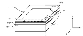
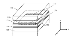
- the manufacturing method of the thermoelectric conversion element according to the present invention is as follows: Forming a first insulator paste layer provided with a first slit on an oxide thermoelectric conversion material sheet to be a base of the first thermoelectric conversion part; Forming a metal thermoelectric conversion material paste layer covering the first slit on the first insulator paste layer; Forming a second insulator paste layer around the metal thermoelectric conversion material paste layer on the first insulator paste layer; Covering the metal thermoelectric conversion material paste layer and the second insulator paste layer, forming a third insulator paste layer provided with a second slit; Producing a laminate including the oxide thermoelectric conversion material sheet, the metal thermoelectric conversion material paste layer, the first insulator paste layer, the second insulator paste layer, and the third insulator paste layer; Firing the laminate.
- the insulator layer covers the end face of the second thermoelectric conversion part, and the second thermoelectric conversion part is not exposed to the outer surface of the thermoelectric conversion element.
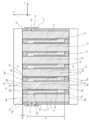
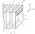
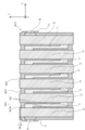
- FIG. 2 is a cross-sectional view of the thermoelectric conversion element according to the embodiment, taken along line AA in FIG. 1.
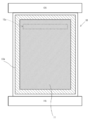
- FIG. 3 is a cross-sectional view of the thermoelectric conversion element according to the embodiment, taken along line BB in FIG. 1.
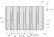
- 6 is a cross-sectional view of a thermoelectric conversion element according to Comparative Example 1.
- FIG. 6 is a cross-sectional view of a thermoelectric conversion element according to Comparative Example 2.
- FIG. 4 is a partial SEM photograph of a thermoelectric conversion element according to Comparative Example 1. It is a perspective view which shows each process of the manufacturing method of the thermoelectric conversion element which concerns on embodiment.
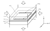
- thermoelectric conversion element which concerns on embodiment. It is a perspective view which shows each process of the manufacturing method of the thermoelectric conversion element which concerns on embodiment. It is a perspective view which shows each process of the manufacturing method of the thermoelectric conversion element which concerns on embodiment. It is a perspective view which shows each process of the manufacturing method of the thermoelectric conversion element which concerns on embodiment. It is a perspective view which shows each process of the manufacturing method of the thermoelectric conversion element which concerns on embodiment. It is a perspective view which shows each process of the manufacturing method of the thermoelectric conversion element which concerns on embodiment. 10 is a cross-sectional view of a thermoelectric conversion element according to Comparative Example 3.
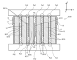
- FIG. It is a partial perspective view of the thermoelectric conversion element which concerns on a modification. It is a partial cross section figure of the thermoelectric conversion element which concerns on a modification. It is sectional drawing of the thermoelectric conversion element which concerns on a modification. It is sectional drawing of the thermoelectric conversion element which concerns on a modification. It is a side view at the time of seeing the thermoelectric conversion element concerning
- thermoelectric conversion element according to an embodiment of the present invention will be described in detail with reference to the drawings.
- the thermoelectric conversion element 10 includes a plurality of first thermoelectric conversion units 13, a plurality of second thermoelectric conversion units 11, a plurality of insulator layers 15, A laminate including the electrode 16 and the electrode protection member 17.
- the + Z direction in FIG. 1 is described as an upward direction
- the ⁇ Z direction is defined as a downward direction.
- the thermoelectric conversion element 10 includes a heat source HS located on the lower side ( ⁇ Z direction side) and a cold source CS located on the upper side (+ Z direction side in FIG. 1) and having a lower temperature than the heat source. It generates electricity in a state where it is thermally coupled to each.
- the heat source HS and the cold source CS will be described on the assumption that the contact surface with the thermoelectric conversion element 10 is flat.
- a heat sink having a metal flat plate thermally coupled to a heat radiating fin or a refrigerant pipe is employed.
- a metal flat plate thermally coupled to an exhaust heat pipe installed in a factory or the like is employed.
- the some thermoelectric conversion element 10 may be used in the state connected in series or parallel.
- the plurality of first thermoelectric converters 13 are foil-shaped.
- the several 2nd thermoelectric conversion part 11 is foil shape.
- the plurality of first thermoelectric converters 11 and the plurality of second thermoelectric converters 13 are alternately arranged and joined via insulator layers 15 in one direction (Y-axis direction in FIG. 1). Specifically, the first thermoelectric conversion unit 11 and the front second thermoelectric conversion unit 13 are directly joined in a partial region of the joint surface between the first thermoelectric conversion unit 13 and the front second thermoelectric conversion unit 11. In the other region of the joining surface, the first thermoelectric conversion unit 11 and the second thermoelectric conversion unit 13 are joined via the insulator layer 15.
- the 2nd thermoelectric conversion part 11 is electrically connected to the lower end part 13a of the 1st thermoelectric conversion part 13 which the lower end part (end part by the side of the 2nd direction) 11a adjoins by + Y direction.
- the second thermoelectric conversion unit 11 has an upper end (end on the third direction side) 11b electrically connected to the upper end 13b of the first thermoelectric conversion unit 13 adjacent in the ⁇ Y direction. Then, two surfaces (first main surface and second main surface) located at both ends in the Y-axis direction from the plurality of first thermoelectric conversion units 13, the plurality of second thermoelectric conversion units 11 and the insulator layer 15.
- the first thermoelectric converter 13 has end faces 13c and 13d orthogonal to the Z-axis direction at both ends in the Z-axis direction.
- the end faces 13c and 13d of each of the plurality of first thermoelectric converters 13 are formed so that they exist in the same plane. That is, the end faces 13c and 13d of each of the plurality of first thermoelectric converters 13 are flush with each other.
- the first thermoelectric conversion unit 13 is an oxide semiconductor.
- the oxide semiconductor includes, for example, a composite oxide represented by a composition formula: ATiO 3 having a perovskite structure. Such a composition is defined as an N-type semiconductor.
- a in the composition formula: ATiO 3 is the one in which Sr is replaced with La in La 1-x Sr x in the range of 0 ⁇ x ⁇ 0.2, for example (Sr 0.965 La 0.035 ) TiO 3 may be used.
- An N-type semiconductor containing this composite oxide is chemically stable against corrosive gases such as hydrogen sulfide and oxidizing gases.
- the second thermoelectric conversion unit 11 includes, for example, a NiMo alloy and a composite oxide represented by a composition formula: ATiO 3 having a perovskite structure. Such a composition is defined as a P-type semiconductor. In other words, the second thermoelectric conversion unit 11 is defined as a semiconductor containing a metal.
- a in the composition formula: ABO 3 is obtained by replacing Sr with La in the range of 0 ⁇ x ⁇ 0.2 in La 1-x Sr x , for example, (Sr 0.965 La 0.035 ) TiO 3 3 may be sufficient.
- the insulator layer 15 includes a first insulator portion 15b and a second insulator portion 15a.
- the first insulator portion 15b and the second insulator portion 15a are integrally molded.
- the second insulator portion 15a is interposed between the first thermoelectric conversion portion 13 and the second thermoelectric conversion portion 11 that are adjacent in the Y-axis direction.
- the 1st thermoelectric conversion part 13 and the 2nd thermoelectric conversion part 11 are mutually joined through the through-hole 15c formed in the insulator part 15a.
- the first insulator portion 15b covers the ends of the second thermoelectric conversion portion 11 in the ⁇ X direction and ⁇ Z direction.
- the first insulator portion 15b is disposed so as to surround the second thermoelectric conversion portion 11 as shown in FIG. 3 when viewed in a section taken along line BB in FIG. Further, the first insulator portion 15b has a concave portion 15d that is recessed toward the center portion side in the Z-axis direction of the second thermoelectric conversion portion 11 from both end faces 13c and 13d in the Z-axis direction of the first thermoelectric conversion portion 13. Have.
- the end surface of the insulator layer 15 is formed with a recess 15d that is recessed toward the center in the X-axis direction and the Z-axis direction of the laminate from the end surface in the X-axis direction and the Z-axis direction of the first thermoelectric conversion unit 13. ing.
- the depth D1 from the end surfaces 13c and 13d to the deepest part of the recessed part 15d is set to 10 micrometers or less, for example.
- each 1st insulator part 15b does not contact cold source CS and heat source HS by having crevice 15d.
- the end surfaces 13c and 13d of the plurality of first thermoelectric conversion units 13 are flush with each other, the end surfaces 13c of the plurality of first thermoelectric conversion units 13 are in surface contact with the heat source HS. And the end surface 13d of each of the plurality of first thermoelectric converters 13 is in surface contact with the cold source CS.
- the insulator layer 15 is formed from an oxide insulator material having electrical insulation.
- this oxide insulator material for example, ZrO 2 (yttria stabilized zirconia) to which Y 2 O 3 is added as a stabilizer is employed.
- the oxide insulator material containing ZrO 2 is chemically stable against a corrosive gas such as hydrogen sulfide or an oxidizing gas.
- the electrode 16 includes a first thermoelectric conversion unit 13 positioned at the end in the + Y direction among the plurality of first thermoelectric conversion units 13 and a first thermoelectric conversion unit 13 positioned at the end in the ⁇ Y direction (fourth direction). 1 thermoelectric conversion unit 13 is provided.
- the electrodes 16 are respectively provided on both end surfaces (first main surface and second main surface) in the Y-axis direction of the multilayer body.
- the center C1 of the electrode 16 is located on the + Z direction side of the first thermoelectric converter 13 in the Z-axis direction, that is, on the side closer to the cold source CS.
- the electrode 16 passes through the center of the line segment connecting the both end surfaces in the Z-axis direction of the first thermoelectric converter 13 on both end surfaces in the Y-axis direction of the multilayer body in plan view from the Y-axis direction and the first.
- a virtual line parallel to both end faces in the Z-axis direction of the thermoelectric conversion element 13 and a virtual line passing through the center C1 of the electrode 16 and parallel to both end faces in the Z-axis direction of the first thermoelectric conversion element 13 are positioned differently. It is provided to do.
- the electrode 16 includes a base layer made of Ni and a contact layer that covers the base layer.
- the contact layer has a stacked structure of a Ni layer and a Sn layer.
- the thickness of the Ni layer is set to 3 to 5 ⁇ m, and the thickness of the Sn layer is set to 4 to 6 ⁇ m.
- a lead wire (not shown) for taking out electric power generated by the thermoelectric conversion element 10 is bonded to the electrode 16.
- the lead wire connected to the electrode 16 is connected to, for example, a power management circuit or a wireless communication circuit.
- the thermoelectric conversion element 10 functions as a driving power source for the power management circuit and the wireless communication circuit.
- the electrode protection member 17 covers the periphery of the electrode 16. Specifically, the electrode protection member 17 covers the periphery of the electrode 16 and the first main surface and the second main surface of the laminate.
- the electrode protection member 17 is formed from an oxide insulator material having electrical insulation.
- this oxide insulator material for example, ZrO 2 (yttria-stabilized zirconia) to which Y 2 O 3 is added as a stabilizer is employed as in the insulator layer 15.
- thermoelectric conversion element 10 in the ⁇ Z direction
- the cold source CS is in contact with the end surface of the thermoelectric conversion element 10 in the + Z direction.
- electrons move in the + Z direction in the first thermoelectric conversion unit 13 to generate a current flowing in the ⁇ Z direction
- holes move in the + Z direction in the second thermoelectric conversion element 11 and flow in the + Z direction. Occurs.
- a current flowing in the + Y direction is generated in the thermoelectric conversion element 10.
- thermoelectric conversion element 10 The inventors evaluated the corrosion resistance and the electrode shape dependency of the power generation amount of the thermoelectric conversion element 10 according to the present embodiment and the thermoelectric conversion elements according to Comparative Examples 1 and 2 described later.
- the evaluation of the adhesion strength of the electrode was performed using two types of evaluation samples. One of them is a first sample simulating the first thermoelectric converter 13 provided with the electrode 16 of the thermoelectric conversion element 10, and the other is the first thermoelectric converter 13 provided with the electrode 16. 2 is a second sample simulating a configuration without the electrode protection member 17.
- the evaluation thermoelectric conversion element, the first sample, and the second sample prepared by the inventors will be described.
- thermoelectric conversion element 10 As the thermoelectric conversion element 10 according to the present embodiment, the length in the X-axis direction is about 6 mm, the length in the Y-axis direction is about 7 mm, and the length in the Z-axis direction is about 2.7 mm.
- a portion 11 having 50 layers and a first thermoelectric conversion portion 13 having 51 layers was prepared.
- the thickness of the second thermoelectric conversion part 11 was set to about 200 ⁇ m, the thickness of the first thermoelectric conversion part 13 was set to about 30 ⁇ m, and the thickness of the second insulator part 15a was set to about 5 ⁇ m.
- thermoelectric conversion element 9010 in the thermoelectric conversion element 9010 according to Comparative Example 1, a part of the second thermoelectric conversion unit 9011 is exposed on the outer surface of the thermoelectric conversion element 9010.
- FIG. 4A the same components as those in the embodiment are given the same reference numerals as those in FIG.
- the external dimensions of the thermoelectric conversion element 9010, the number of the first thermoelectric conversion sections 13, and the thickness of the first thermoelectric conversion sections 13 were the same as those of the thermoelectric conversion element 10 for evaluation described above.
- the number of second thermoelectric conversion units 9011, the thickness of the second thermoelectric conversion units 9011, and the insulator layer 9015 are the same as the number of second thermoelectric conversion units 11 of the thermoelectric conversion element 10 for evaluation described above, and the second thermoelectric conversion.
- the thickness is the same as that of the portion 11 and the second insulator portion 15a.
- thermoelectric conversion element 9110 according to Comparative Example 2 is provided so that the electrode 9116 covers the entire surface of the first thermoelectric conversion unit 13 that is orthogonal to the Y-axis direction.
- FIG. 4B the same configurations as those in Comparative Example 1 are denoted by the same reference numerals as in FIG. 4A.
- the external dimensions of the thermoelectric conversion element 9110, the number of the second thermoelectric conversion units 9011 and the first thermoelectric conversion units 13, and the thicknesses of the second thermoelectric conversion units 9011, the first thermoelectric conversion units 13 and the insulator layer 9015 are as described above.
- the thermoelectric conversion element 9010 for evaluation was used.
- the first sample includes a base material made of an N-type oxide semiconductor material, an electrode having a rectangular shape in plan view provided on one surface of the base material, a peripheral edge of the electrode, a first main surface of the laminate, and a second main surface.
- An electrode protection member formed to cover the surface.
- This first sample was fired after applying a later-described Ni paste to be a base for an electrode underlayer and an insulator paste to be a base for an electrode protection member to an N-type oxide semiconductor material sheet to be described later. It was produced by forming a contact layer covering the underlayer by electroplating.
- the shape of the electrode was a square shape in plan view, and its dimensions were 2 mm ⁇ 2 mm.
- the second sample includes a base material made of an N-type oxide semiconductor material and a rectangular electrode in plan view provided on one surface of the base material.
- This second sample is a N-type oxide semiconductor sheet, which will be described later, applied with a Ni paste, which will be described later, which serves as the base of the electrode, and then fired, and then a contact layer that covers the underlying layer by electroplating. It was produced by forming.
- the shape of the electrode was a square shape in plan view, and its dimensions were 2 mm ⁇ 2 mm.
- thermoelectric conversion element 10 and thermoelectric conversion element 9010 in which second thermoelectric conversion portion 9011 is exposed to the outside.
- twelve thermoelectric conversion elements 10 and 9010 for evaluation were prepared, and a gas corrosion test was performed on them.
- an output voltage (initial voltage) before exposure to a corrosive gas is measured, and then a test tank maintained in an atmosphere in which the corrosive gas is dispersed. The sample was allowed to stand for 240 hours, and then the output voltage (post-exposure voltage) was measured again.
- the average value of the initial voltage was compared with the average value of the voltage after exposure.
- H 2 S and SO 2 were adopted as corrosive gases. Further, the inside of the test tank was maintained in an atmosphere having a H 2 S concentration of 3 ppm, a SO 2 concentration of 10 ppm, a temperature of 40 ° C., and a humidity of 85%.
- the conditions of this gas corrosion test are conditions assuming general outdoor use (excluding use in areas with a large environmental load such as a hot spring area) defined by the technical standard DN8J112A.
- the output voltage is measured by maintaining the temperature of the heat source in contact with the lower side of the thermoelectric conversion elements 10 and 9010 at 30 ° C. and the temperature of the cold source CS in contact with the upper side of the thermoelectric conversion elements 10 and 9010 at 20 ° C. It was done in a maintained state.
- thermoelectric conversion elements 10 and 9010 after being exposed to a corrosive gas by SEM observation, analysis of precipitates using ⁇ -XRD (X-Ray Diffractometry), and WDX (wavelength-dispersive). Component analysis was performed using X-ray (spectrometry). In component analysis using WDX, the upper end surface of the thermoelectric conversion element 9010 is polished by a predetermined depth, and then the distribution of S (sulfur) component on the polished surface is repeatedly measured by WDX. The penetration depth into the thermoelectric conversion element 9010 was examined.
- thermoelectric conversion element 9010 As a result of measuring the output voltage, in the thermoelectric conversion element 9010, the average value of the initial voltage was 66 mV, and the average value of the post-exposure voltage was 10 mV. On the other hand, in the thermoelectric conversion element 10, the average value of the initial voltage was 63 mV, and the average value of the post-exposure voltage was 63 mV. As described above, in the thermoelectric conversion element 9010, the average value of the post-exposure voltage is 56 mV lower than the average value of the initial voltage, whereas in the thermoelectric conversion element 10, the average value of the post-exposure voltage and the average value of the initial voltage are reduced. And the same.
- the average value of the initial voltage of the thermoelectric conversion element 10 is 3 mV lower than the average value of the initial voltage of the thermoelectric conversion element 9010 because the length L1 of the second thermoelectric conversion unit 11 in the Z-axis direction is the second thermoelectric conversion unit. This is because 9011 is shorter than the length L2 in the Z-axis direction. If the length L1 of the second thermoelectric conversion unit 11 in the Z-axis direction is equal to the length L2 of the second thermoelectric conversion unit 9011 in the Z-axis direction, the output voltage of the thermoelectric conversion element 10 is also the output voltage of the thermoelectric conversion element 9010. Is equivalent to
- thermoelectric conversion element 9010 when the surface of the thermoelectric conversion element 9010 was observed by SEM, it was confirmed that precipitates exist on the surface of the thermoelectric conversion element 9010 as shown by SC in FIG. This precipitate was confirmed to be nickel sulfate hydrate by analysis using ⁇ -XRD. Further, from component analysis using WDX, S element contained in the nickel sulfate hydrate is present in the entire second thermoelectric conversion unit 9011, and S element is present in the first thermoelectric conversion unit 13 and the insulator layer 9015. It was confirmed not to. On the other hand, observation of the surface of the thermoelectric conversion element 10 by SEM confirmed that no precipitate was present on the surface of the thermoelectric conversion element 10. Moreover, in the component analysis using WDX, it was confirmed that S element does not exist in any of the 2nd thermoelectric conversion part 11, the 1st thermoelectric conversion part 13, and the insulator layer 15. FIG.
- thermoelectric conversion element 9010 the second thermoelectric conversion part 9011 containing Ni is exposed on the outer surface of the thermoelectric conversion element 9010, as shown in a portion AR1 surrounded by a broken line in FIG. 4A. Therefore, when the thermoelectric conversion element 9010 is exposed to a corrosive gas such as sulfur, Ni contained in the second thermoelectric conversion portion 9011 reacts with the corrosive gas to form nickel sulfate hydrate. End up. When such impurities are formed in the second thermoelectric conversion unit 9011, the movement of carriers in the second thermoelectric conversion unit 9011 is hindered, and the output voltage of the thermoelectric conversion element 9010 decreases.
- a corrosive gas such as sulfur
- thermoelectric conversion element 10 in the case of the thermoelectric conversion element 10, as shown in FIG. 1 and FIG. 2, the ends of the second thermoelectric conversion unit 11 in the ⁇ X direction and ⁇ Y direction are covered with the first insulator 15b. It is not exposed on the outer surface of the thermoelectric conversion element 10.
- the first thermoelectric conversion unit 13 and the insulator layer 15 do not contain the S element, the second thermoelectric conversion unit 13 and the insulator layer The material forming 15 is less likely to react with corrosive gases. Thereby, since it is difficult for impurities to be formed in the second thermoelectric conversion unit 11, fluctuations in the output voltage of the thermoelectric conversion element 10 before and after exposure to the corrosive gas are suppressed.
- thermoelectric conversion elements 10 and 9110 for evaluation were prepared, and the output voltage was measured for them.
- the twelve thermoelectric conversion elements 10 for evaluation are prepared separately from the twelve thermoelectric conversion elements 10 used for evaluation of corrosion resistance.
- the shapes of the electrodes 16 and 9116 are different from each other as described above.
- the output voltage is measured by maintaining the temperature of the heat source HS in contact with the lower side of the thermoelectric conversion elements 10 and 9110 at 30 ° C. and the temperature of the cold source CS in contact with the upper side of the thermoelectric conversion elements 10 and 9010 at 20 ° C. It was done in a maintained state.
- thermoelectric conversion element 9110 As a result of measuring the output voltage, in the thermoelectric conversion element 9110, the average value of the output voltage was 66 mV. On the other hand, in the thermoelectric conversion element 10, the average value of the output voltage was 70 mV. Thus, it was found that the output voltage of the thermoelectric conversion element 10 was higher by about 4 mV than the output voltage of the thermoelectric conversion element 9110.
- thermoelectric conversion element 9110 As shown in FIG. 4B, electrode 9116 is provided so as to cover the entire surface orthogonal to the Y-axis direction of first thermoelectric conversion unit 13.
- the material forming the electrode 9116 is metal, and the thermal conductivity thereof is higher than the thermal conductivity of the material forming the second thermoelectric conversion unit 9011 and the first thermoelectric conversion unit 13.
- the electrode 16 of the thermoelectric conversion element 10 is provided in a part of the first thermoelectric conversion unit 13, and the end of the thermoelectric conversion element 10 from the ⁇ Z direction end to the + Z direction end. Not a heat transport route to.
- the amount of heat transported from the ⁇ Z direction end of the thermoelectric conversion element 9110 to the + Z direction end is + Z from the ⁇ Z direction end of the thermoelectric conversion element 10 by the amount of the electrode 9116 interposed. Larger than the amount of heat transported to the end of the direction.
- the electrode 16 is located on the + Z direction side of the first thermoelectric conversion unit 13 in the Z-axis direction, that is, on the side closer to the cold source CS. Thereby, the heat at the end in the + Z direction of the thermoelectric conversion element 10 is easily radiated to the outside through the electrode 16, and accordingly, the temperature at the end in the + Z direction of the thermoelectric conversion element 10 is hardly increased. It has become.
- thermoelectric conversion element 10 the temperature difference between the ⁇ Z direction end of the thermoelectric conversion element 10 and the + Z direction end is the temperature difference between the ⁇ Z direction end and the + Z direction end of the thermoelectric conversion element 9110. Compared to larger. Therefore, the output voltage of the thermoelectric conversion element 10 is higher than the output voltage of the thermoelectric conversion element 9110.
- the electrode protection member 17 is provided, so that the peeling of the electrode 16 is suppressed as compared with the case where the electrode protection member 17 is not provided.
- thermoelectric conversion element 10 As described above, according to the thermoelectric conversion element 10 according to the present embodiment, as shown in FIGS. 1 and 2, the ends of the second thermoelectric conversion unit 11 in the ⁇ X direction and the ⁇ Z direction are corroded.
- the second thermoelectric conversion portion 11 is not exposed to the outer surface of the thermoelectric conversion element 10 because it is covered with the first insulator portion 15 b that is chemically stable against the reactive gas. This prevents the material forming the second thermoelectric conversion part 11 from chemically reacting with the corrosive gas existing around the thermoelectric conversion element 10 to form impurities in the second thermoelectric conversion part 11. . Accordingly, the deterioration of the electrical characteristics of the thermoelectric conversion element 10 due to the corrosive gas existing around the thermoelectric conversion element 10 is suppressed.
- thermoelectric conversion element 9010 which concerns on the comparative example 1
- the structure provided with the insulator layer which is chemically stable with respect to corrosive gas and covers the whole thermoelectric conversion element 9010 can be considered.
- the insulating layer prevents the corrosive gas existing around the thermoelectric conversion element 9010 from contacting the second thermoelectric conversion unit 9011.
- a step of forming an insulator layer covering the entire thermoelectric conversion element 9010 is required, and the number of steps increases.
- thermoelectric conversion element 10 since the insulator layer that covers the entire thermoelectric conversion element 10 is not provided, the step of forming the insulator layer that covers the entire thermoelectric conversion element 10 is formed. Is unnecessary. This can simplify the manufacturing method by reducing the number of steps.
- the electrode 16 of the thermoelectric conversion element 10 is provided in a part of the first thermoelectric conversion unit 13, and the end of the thermoelectric conversion element 10 in the ⁇ Z direction. It does not become a heat transport path from to the end in the + Z direction. Further, the electrode 16 is located on the + Z direction side of the first thermoelectric conversion unit 13 in the Z-axis direction, that is, on the side closer to the cold source CS. Thereby, the heat at the end in the + Z direction of the thermoelectric conversion element 10 is easily radiated to the outside through the electrode 16, and accordingly, the temperature at the end in the + Z direction of the thermoelectric conversion element 10 is hardly increased. It has become.
- thermoelectric conversion element 10 the temperature difference between the ⁇ Z direction end of the thermoelectric conversion element 10 and the + Z direction end is the temperature difference between the ⁇ Z direction end and the + Z direction end of the thermoelectric conversion element 9110. Compared to larger. Therefore, the output voltage of the thermoelectric conversion element 10 is higher than the output voltage of the thermoelectric conversion element 9110.
- the electrode protection member 17 is provided so as to cover the periphery of the electrode 16. Since it is firmly fixed by the first thermoelectric conversion unit 13 via the protective member 17, peeling of the electrode 16 is suppressed.
- the electrode protection member 17 is provided so as to cover the periphery of the electrode 16 in order to suppress peeling from the periphery of the electrode 16. Thereby, the periphery of the electrode 16 is firmly fixed to the first thermoelectric conversion unit 13 via the electrode protection member 17. Thereby, peeling of the electrode 16 when a thermal shock is applied to the thermoelectric conversion element 10 is suppressed.
- the first insulator portion 15b is formed of an oxide insulator material containing ZrO 2 that is chemically stable against a corrosive gas such as hydrogen sulfide.
- the first thermoelectric converter 13 is also formed of an N-type semiconductor containing a complex oxide that is chemically stable to corrosive gases. Thereby, even if the thermoelectric conversion element 10 is used in an atmosphere in which hydrogen sulfide is dispersed, the formation of sulfide in the second thermoelectric conversion unit 11 is prevented.
- thermoelectric conversion element 10 Next, a method for manufacturing the thermoelectric conversion element 10 according to the present embodiment will be described with reference to FIGS. 6A to 6C and FIGS. 7A to 7C.
- this manufacturing method first, an N-type oxide semiconductor material sheet that is the basis of the first thermoelectric conversion portion 13, a P-type semiconductor material paste that is the basis of the second thermoelectric conversion portion 11, the insulator layer 15 and the electrode protection An insulating paste as a base of the member 17 is generated.
- the N-type oxide semiconductor material sheet In the production of the N-type oxide semiconductor material sheet, first, La 2 O 3 , SrCO 3 , and TiO 2 are weighed so that their molar ratio is 0.965: 0.035: 1. Next, pure water is added to the weighed powder materials of La 2 O 3 , SrCO 3 , and TiO 2 and then pulverized and mixed using a ball mill to obtain a slurry containing La 2 O 3 , SrCO 3 , and TiO 2. Generate. Then, after drying the produced
- the particle size of the powder material is not particularly limited, but is preferably determined so that La 2 O 3 , SrCO 3 , and TiO 2 are uniformly mixed.
- the method of calcination is not particularly limited.
- the temperature of calcination is not limited to 1300 degreeC, Other temperature may be sufficient as long as it is 1000 degreeC or more.
- the aforementioned (Sr 0.965 La 0.035 ) TiO 3 powder material, Ni powder material, and Mo powder material are weighed. Specifically, the molar ratio of Ni and Mo is 0.9: 0.1, the combined weight ratio of Ni and Mo is 80 wt%, and (Sr 0.965 La 0.035 ) TiO 3 powder material. Weigh so that the weight ratio is 20 wt%. Subsequently, (Sr 0.965 La 0.035 ) TiO 3 powder material, Ni powder material, Mo powder material, and organic solvent such as varnish are mixed using a roll machine or the like, thereby (2) A P-type semiconductor material paste that is the basis of the thermoelectric conversion unit 11 is generated.
- the particle sizes of the Ni powder material and the Mo powder material are not particularly limited, but the powder material of (Sr 0.965 La 0.035 ) TiO 3 , the Ni powder material, and the Mo powder material are uniformly mixed. It is preferable to be determined as follows.
- Insulating paste is weighed Y 2 O 3 ZrO 2 powder material that has been added, and the ZrO 2 powder material Y 2 O 3 is added, and an organic solvent varnish, using a roll mill or the like And mixed.
- the average particle diameter of the ZrO 2 powder material is set so that the time until the sintering of the insulator paste is completed is longer than the time until the sintering of the N-type oxide semiconductor sheet is completed during firing. .
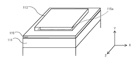
- a first insulator paste layer 115 is formed on the N-type oxide semiconductor material sheet 111.
- the thickness of the first insulator paste layer 115 is, for example, 5 ⁇ m.
- the first insulator paste layer 115 is formed such that the first slit 115a is provided in a portion corresponding to the joint portion between the first thermoelectric conversion portion 13 and the second thermoelectric conversion portion 11 in the N-type oxide semiconductor material sheet 111. Is done.
- a P-type semiconductor material paste layer 113 is formed on the first insulator paste layer 115 as shown in FIG. 6B.
- the thickness of the P-type semiconductor material paste layer 113 is, for example, 50 ⁇ m.
- the P-type semiconductor material paste layer 113 is formed so as to cover the first slit 115 a of the first insulator paste layer 115.
- a second insulator paste layer 116 is formed around the P-type semiconductor material paste layer 113 on the first insulator paste layer 115.
- the second insulator paste layer 116 has the same thickness as the P-type semiconductor material paste layer 113.
- a third insulator paste layer 117 is formed so as to cover the P-type semiconductor material paste layer 113 and the second insulator paste layer 116.
- the thickness of the third insulator paste layer 117 is 5 ⁇ m, for example.
- the portion corresponding to the joint portion between the first thermoelectric conversion unit 13 and the second thermoelectric conversion unit 11 located at the ⁇ Z direction end of the P-type semiconductor material paste layer 113 of the third insulator paste layer 117 includes the first Two slits 117a are formed.
- an N-type oxide semiconductor material sheet 111 is laminated on the third insulator paste layer 117.
- a plurality of sheets are laminated.
- the N-type oxide semiconductor material sheets 111 corresponding to the first thermoelectric conversion portions 13 positioned at both ends in the Y-axis direction of the thermoelectric conversion element 10 are preliminarily provided.
- the Ni paste as the base of the electrode 16 and the insulator paste as the base of the electrode protection member 17 are applied. These are the bases of the electrode protection member 17 so as to cover the periphery of the portion where the Ni paste is applied after applying the Ni paste which is the base of the electrode 16 to the N-type oxide semiconductor material sheet 111 and drying it.
- the insulating paste is applied and then dried.
- the Ni paste is generated by mixing Ni powder material and an organic solvent such as varnish.
- an N-type oxide semiconductor material sheet in which a P-type semiconductor material paste layer 113 and insulator paste layers 115, 116, and 117 are formed using an isotropic isostatic pressing method.
- a laminated body is produced by pressure bonding 111.
- This stacked body includes an N-type oxide semiconductor material sheet 111, a P-type semiconductor material paste layer 113, a first insulator paste layer 115, a second insulator paste layer 116, and a third insulator paste layer 117.
- generated laminated body is cut
- the individual pieces of the laminated body are formed in a rectangular parallelepiped shape of 4 mm ⁇ 3.2 mm ⁇ 3.2 mm, for example.
- the individual pieces of the laminate are subjected to a reducing atmosphere with an oxygen partial pressure of 10 ⁇ 10 to 10 ⁇ 15 MPa and a temperature of 1200 ° C. to 1400 ° C. Bake.
- a firing method a hot press sintering method, an SPS (Spark Plasma Sintering) sintering method, an HIP (Hot Isostatic Pressing) sintering method, or the like may be employed.
- the oxygen partial pressure may be another oxygen partial pressure as long as Ni is not oxidized and the thermoelectric characteristics of the first thermoelectric conversion unit 13 are not greatly reduced.
- the firing temperature is such that the relative density of the main components of the second thermoelectric conversion unit 11, the first thermoelectric conversion unit 13, and the insulator layer 15 is 80% or more, and the N-type oxide semiconductor material sheet 111, P-type Other temperatures may be used as long as the semiconductor material paste layer 113 and the insulator paste layers 115, 116, and 117 are co-sintered.
- the average particle diameter of the ZrO 2 powder material contained in the insulator paste is such that the time until the sintering of the insulator paste is completed is the time when the N-type oxide semiconductor material sheet 111 is sintered. It is set to be longer than the time until completion.
- the outer surface of the first insulator portion 15 b has a shape that is recessed toward the inside of the thermoelectric conversion element 10 from the outer surface of the first thermoelectric conversion portion 13.
- thermoelectric conversion element 10 is completed.
- the number of firings can be reduced to one, so that the manufacturing process can be simplified.
- thermoelectric conversion element 9010 which concerns on the comparative example 1 is produced with the following manufacturing methods.
- an insulating paste is applied to the N-type oxide semiconductor material sheet and the P-type semiconductor material sheet using a printing technique.
- the N-type oxide semiconductor material sheet and the P-type semiconductor material sheet coated with the insulator paste are alternately laminated, and then the Ni paste as the basis of the electrode 16 and the insulator as the basis of the electrode protection member 17 Paste Ni paste is applied and these are pressure-bonded to produce a laminate. Thereafter, the laminate is cut into individual pieces and fired.
- the periphery of the 2nd thermoelectric conversion part 9211 may be in the state which protruded from the outer surface of the thermoelectric conversion element 9210 like the thermoelectric conversion element 9210 which concerns on the comparative example 3 shown in FIG.
- the protruding portion of the second thermoelectric conversion portion 9211 (see the portion Po2 surrounded by the broken line in FIG. 8) is in contact with the heat source HS and the cold source CS, but the area of this contact portion is relatively small and is from the heat source HS.
- the heat transfer efficiency to the end in the ⁇ Z direction of the thermoelectric conversion element 9210 and the heat transfer efficiency from the end in the + Z direction of the thermoelectric conversion element 9210 to the cold source CS are low.
- the temperature difference between both ends in the Z-axis direction of the thermoelectric conversion element 9210 becomes smaller than the temperature difference between the heat source HS and the cold source CS, and the output voltage of the thermoelectric conversion element 9210 decreases accordingly. End up.
- thermoelectric conversion element 9010 in the method for manufacturing the thermoelectric conversion element 9010 according to Comparative Example 1, a polishing step is performed in which the both ends in the Z-axis direction of the thermoelectric conversion element 9210 are flattened after firing.
- output voltages in a state before polishing both ends in the Z-axis direction were measured. In the measurement of the output voltage, the temperature of the heat source in contact with the lower side of the thermoelectric conversion elements 10 and 9010 was maintained at 30 ° C., and the temperature of the cold source in contact with the upper side of the thermoelectric conversion elements 10 and 9010 was maintained at 20 ° C. Made in state.
- the average value of the output voltage obtained by the measurement was 35 mV, which was about half the average value 66 mV of the output voltage of the thermoelectric conversion element 9010 after the above-described polishing. From this, it can be seen that in the method for manufacturing the thermoelectric conversion element 9010 according to Comparative Example 1, the above-described polishing step is essential.
- thermoelectric conversion element 10 by adjusting the average particle diameter of the ZrO 2 powder material included in the insulator paste, it is shown in FIG.
- the outer surface of the first insulator portion 15 b is shaped to be recessed toward the inner side of the thermoelectric conversion element 10 than the outer surface of the first thermoelectric conversion portion 13.
- the end surfaces 13c and 13d of the first thermoelectric converter 13 are in surface contact with the heat source HS and the cold source CS.
- the area of the contact portion of the first thermoelectric conversion unit 13 is larger than the area of the contact portion of the thermoelectric conversion element 9010, and the heat transfer efficiency and thermoelectric power from the heat source HS to the end in the ⁇ Z direction of the thermoelectric conversion element 10 are increased.
- the heat transfer efficiency from the + Z direction end of the conversion element 10 to the cold source CS is relatively high.
- the average value of the output voltages of the twelve evaluation thermoelectric conversion elements 10 according to the present embodiment is 63 mV, which is approximately the same as the average value 66 mV of the output voltage of the thermoelectric conversion element 9010. It can also be seen that the heat transfer efficiency between the thermoelectric conversion element 10, the heat source HS, and the cold source CS is relatively high. Accordingly, the manufacturing method of the thermoelectric conversion element 10 eliminates the above-described polishing step, which is essential in the manufacturing method of the thermoelectric conversion element 9010, and thus the manufacturing method can be simplified correspondingly.
- the present invention is not limited to the configuration of the above-described embodiment.
- the electrode protection member 2017 may be formed so that the thickness of the end in the + Z direction is thick.
- the same reference numerals as those in FIGS. 1 and 2 are assigned to the same configurations as those in the embodiment.
- the heat at the periphery of the electrode 16 is transmitted to the cold source CS via the electrode protection member 2017, as indicated by a broken line arrow A1 in FIG. 9B. Thereby, the temperature fluctuation
- the size of the electrode protection member 17 shown in FIG. 2 is not particularly limited as long as it covers the periphery of the electrode 16.
- the first insulator 4015 b may be a thermoelectric conversion element 4010 that does not cover a part of the side surface (surface in the Y-axis direction) of the first thermoelectric conversion unit 13. That is, the thermoelectric conversion element 4010 in which the side surface of the first thermoelectric conversion unit 13 is exposed may be used.
- the same reference numerals as those in FIG. 2 are assigned to the same configurations as those in the first embodiment.
- a width W2 between the end surface in the Z-axis direction of the first thermoelectric conversion unit 13 and the end surface in the Z-axis direction of the first insulator 4015b can be set to about 10 ⁇ m, for example.
- the first thermoelectric conversion unit 13 is exposed without being covered by the first insulator 4015b.
- the contact area between the heat source HS and the cold source CS can be increased by the presence of the end portion in the direction.
- thermoelectric conversion element 10 including the electrode protection member 17 that covers the entire periphery of the electrode 16
- the electrode protection member is not necessarily limited to the one that covers the entire periphery of the electrode 16.
- the lower end edge (edge on the ⁇ Z direction side) of the periphery of the electrode 5016 may not be covered with the electrode protection member 5017.
- the same reference numerals as those in FIG. 2 are assigned to the same configurations as those in the embodiment.
- the lower end of the electrode 5016 is exposed at the lower end surface (end surface on the ⁇ Z direction side) of the thermoelectric conversion element 5010.
- thermoelectric conversion element 5010 When the thermoelectric conversion element 5010 is mounted on a substrate on which a conductive pattern is formed, the electrode 5016 and the conductive pattern are connected with a conductive member such as solder or silver paste in a state where the lower end portion of the electrode 5016 is in contact with the conductive pattern. Can be connected.
- 11 and 12 show an example in which the end portion of the electrode 5016 is in contact with the cold source CS.
- the configuration is not limited thereto, and the end portion of the electrode 5016 is in contact with the heat source HS, for example. It may be. Even in this case, since the electrode 5016 is in contact with the heat source HS, the temperature change in the electrode 5016 is reduced. Accordingly, deterioration of the electrode 5016 due to thermal stress applied to the electrode 5016 is suppressed.
- thermoelectric conversion element 10 In the method for manufacturing the thermoelectric conversion element 10 according to the embodiment, an oxide (La 2 O 3 , TiO 2 ) and carbonate (SrCO 3 ) are used to generate an N-type oxide semiconductor material sheet and a P-type semiconductor material paste.
- an oxide La 2 O 3 , TiO 2
- SrCO 3 carbonate
- the manufacturing method of the thermoelectric conversion element 10 which concerns on embodiment, although the example which uses Ni and Mo as a metal raw material of P-type semiconductor material paste was demonstrated, it replaced with Mo and replaced with Cr (chromium). ) Or W (tungsten) may be used.
- thermoelectric conversion element 10 In the method of manufacturing the thermoelectric conversion element 10 according to the embodiment, an example in which a powder material of ZrO 2 (yttria stabilized zirconia) to which Y 2 O 3 is added as a stabilizer is used to produce an insulator paste.
- the present invention is not limited to this, and can be sintered together with an N-type oxide semiconductor material and a P-type semiconductor material.
- the insulator When an insulator layer is formed by firing an insulator paste in a reducing atmosphere, the insulator Other types of oxides may be used as long as the layer has electrical insulation.
- the stabilizer is not limited to Y 2 O 3 and may be other stabilizers (for example, Ca, Mg, etc.). However, it is preferable to use Y 2 O 3 or Ca as the stabilizer from the materials used for the N-type oxide semiconductor material sheet and the P-type semiconductor material paste and their thermal expansion coefficients.
- the thickness of the N-type oxide semiconductor material sheet is 200 ⁇ m
- the thickness of the P-type semiconductor material paste layer is 50 ⁇ m
- the thickness of the insulator paste layer is 5 ⁇ m
- the thickness of the N-type oxide semiconductor material sheet, the thickness of the P-type semiconductor material paste layer, the thickness of the insulator paste layer, and the number of stacked N-type oxide semiconductor material sheets are not limited thereto. These may be appropriately changed according to the output voltage, output current, and resistance value of the load connected to the thermoelectric conversion element 10 required for the thermoelectric conversion element 10.
- the type of conductive paste on which the electrode 16 is based is not limited to Ni paste as long as it is a material that can be fired simultaneously with the second thermoelectric conversion unit 11 and the first thermoelectric conversion unit 13.
- a conductive paste containing NiMo, Pt, Pd, NiCr, NiW may be used.
- thermoelectric conversion element 10 in which a plurality of film-shaped first thermoelectric conversion sections 13 and a plurality of film-shaped second thermoelectric conversion sections 11 are alternately arranged in the Y-axis direction.
- the structure of the thermoelectric conversion element is not limited to the laminated type.
- a so-called ⁇ -type thermoelectric conversion in which columnar first thermoelectric conversion portions formed of an N-type oxide semiconductor material and columnar second thermoelectric conversion portions formed of a P-type semiconductor material are alternately arranged. It may be an element.
- the insulator may be configured to cover the surface of the second thermoelectric conversion unit so that the surface of the second thermoelectric conversion unit is not exposed to the outside.
- the present invention includes a combination of the embodiments and modifications as appropriate, and a modification appropriately added thereto.
- thermoelectric conversion element 11: second thermoelectric conversion unit, 11a, 11b, 13a, 13b: end, 13: first thermoelectric conversion unit, 13c, 13d: end face, 15: insulator layer 15a: second insulator part, 15b, 4015b: first insulator part, 15c: through hole, 15d: recess, 115a: first slit, 117a: second slit, 16, 5016: electrode, 17, 2017, 5017: Electrode protection member, 111: N-type oxide semiconductor material sheet, 113: P-type semiconductor material paste layer, 115: First insulator paste layer, 116: Second insulator paste layer, 117: Third insulation Body paste layer, HS: heat source, CS: cold source
Landscapes
- Chemical & Material Sciences (AREA)
- Inorganic Chemistry (AREA)
- Engineering & Computer Science (AREA)
- Manufacturing & Machinery (AREA)
- Measuring Temperature Or Quantity Of Heat (AREA)
- Powder Metallurgy (AREA)
Abstract
熱電変換素子(10)は、複数の第1熱電変換部(13)と、複数の第2熱電変換部(11)と、絶縁体層(15)と、を有する積層体を備える。第1熱電変換部(13)と第2熱電変換部(11)とは、Y軸方向において交互に配列し、第1熱電変換部(13)と第2熱電変換部(11)とのY軸方向の面の一部の領域において、第1熱電変換部(13)と第2熱電変換部(11)とが接合し、Y軸方向の面の他の領域において、第1熱電変換部(13)と第2熱電変換部(11)との間に絶縁体層(15)が介在している。積層体は、Y軸方向における両端の第1の主面および第2の主面と、Y軸方向に垂直な方向における両端面と、を有する。絶縁体層(15)は、第2熱電変換部(11)における端面を覆う。
Description
本発明は、熱電変換素子および熱電変換素子の製造方法に関する。
複数のN型の熱電変換部と複数のP型の熱電変換部とが交互に配列してなる熱電変換素子が提案されている(例えば特許文献1参照)。この熱電変換素子は、各熱電変換部の一部が熱電変換素子の外面に露出した構造を有する。また、この種の熱電変換素子には、例えばN型の熱電変換部が酸化物を含むN型酸化物半導体材料から形成され、P型の熱電変換部が金属を含むP型半導体材料から形成されたものがある。
しかしながら、前述の熱電変換素子は、硫化水素等の腐食性ガスが分散した雰囲気中で使用されると、P型の熱電変換部のうち熱電変換素子の外面に露出した部分が腐食性ガスに曝されることになる。そうすると、P型の熱電変換部に含まれる金属と腐食性ガスとが反応してP型の熱電変換部のうち、熱電変換素子の外面に露出した部分に、腐食性ガスの成分を含む不純物が形成されてしまう。この場合、P型の熱電変換部でのキャリアの移動が阻害され、熱電変換素子の出力電圧が低下してしまう。
本発明は、上記事由に鑑みてなされたものであり、P型の熱電変換部が金属を含む材料からなっていたとしても、熱電変換素子における電気的特性の劣化の抑制が可能な熱電変換素子および熱電変換素子の製造方法を提供することを目的とする。
本発明に係る熱電変換素子は、
複数の第1熱電変換部と、複数の第2熱電変換部と、絶縁体層と、を有し、
前記第1熱電変換部と前記第2熱電変換部とが一方向において交互に配列して接合し、
前記第1熱電変換部と前記第2熱電変換部との接合面の一部の領域において、前記第1熱電変換部と前記第2熱電変換部とが直接接合し、前記接合面の他の領域において、前記第1熱電変換部と前記第2熱電変換部との間に前記絶縁体層を介して接合し、
前記一方向における両端に位置する第1の主面および第2の主面と、前記一方向に垂直な方向における両端に位置する端面と、を有する積層体を備え、
前記絶縁体層は、前記第2熱電変換部における端面を覆う。
複数の第1熱電変換部と、複数の第2熱電変換部と、絶縁体層と、を有し、
前記第1熱電変換部と前記第2熱電変換部とが一方向において交互に配列して接合し、
前記第1熱電変換部と前記第2熱電変換部との接合面の一部の領域において、前記第1熱電変換部と前記第2熱電変換部とが直接接合し、前記接合面の他の領域において、前記第1熱電変換部と前記第2熱電変換部との間に前記絶縁体層を介して接合し、
前記一方向における両端に位置する第1の主面および第2の主面と、前記一方向に垂直な方向における両端に位置する端面と、を有する積層体を備え、
前記絶縁体層は、前記第2熱電変換部における端面を覆う。
また、本発明に係る熱電変換素子は、
前記積層体の前記第1の主面および前記第2の主面にそれぞれ設けられた電極を更に備え、
前記電極は、前記一方向から平面視して、前記積層体の対向する一対の前記端面を結ぶ線分の中心を通り且つ前記積層体の端面のうちの少なくとも一方の端面に平行な仮想線と、前記電極の中心を通り且つ前記少なくとも一方の端面に平行な仮想線と、が異なって位置するように設けられている、ものであってもよい。
前記積層体の前記第1の主面および前記第2の主面にそれぞれ設けられた電極を更に備え、
前記電極は、前記一方向から平面視して、前記積層体の対向する一対の前記端面を結ぶ線分の中心を通り且つ前記積層体の端面のうちの少なくとも一方の端面に平行な仮想線と、前記電極の中心を通り且つ前記少なくとも一方の端面に平行な仮想線と、が異なって位置するように設けられている、ものであってもよい。
また、本発明に係る熱電変換素子は、
前記電極の周縁を覆う電極保護部材を更に備える、ものであってもよい。
前記電極の周縁を覆う電極保護部材を更に備える、ものであってもよい。
また、本発明に係る熱電変換素子は、
前記絶縁体層の端面に、前記第1熱電変換部における前記一方向に垂直な方向における端面から該積層体の端面と対向する端面に向かって凹む凹部が形成されている、ものであってもよい。
前記絶縁体層の端面に、前記第1熱電変換部における前記一方向に垂直な方向における端面から該積層体の端面と対向する端面に向かって凹む凹部が形成されている、ものであってもよい。
また、本発明に係る熱電変換素子は、
前記第1熱電変換部における前記一方向に直交する方向の端面から前記絶縁体層における前記一方向に直交する方向の端面までの距離は、10μm以下であってもよい。
前記第1熱電変換部における前記一方向に直交する方向の端面から前記絶縁体層における前記一方向に直交する方向の端面までの距離は、10μm以下であってもよい。
また、本発明に係る熱電変換素子は、
前記第1熱電変換部は、酸化物半導体であり、
前記第2熱電変換部は、金属を含む半導体であり、
前記絶縁体層は、酸化物絶縁体であってもよい。
前記第1熱電変換部は、酸化物半導体であり、
前記第2熱電変換部は、金属を含む半導体であり、
前記絶縁体層は、酸化物絶縁体であってもよい。
また、本発明に係る熱電変換素子は、
前記酸化物半導体は、複合酸化物を含むN型半導体であり、
前記金属を含む半導体は、NiとMoと前記複合酸化物とを含むP型半導体であり、
前記酸化物絶縁体は、ZrO2を含み、
前記複合酸化物は、SrとLaとTiとの少なくとも1つを含む、ものであってもよい。
前記酸化物半導体は、複合酸化物を含むN型半導体であり、
前記金属を含む半導体は、NiとMoと前記複合酸化物とを含むP型半導体であり、
前記酸化物絶縁体は、ZrO2を含み、
前記複合酸化物は、SrとLaとTiとの少なくとも1つを含む、ものであってもよい。
また、本発明に係る熱電変換素子の製造方法は、
第1熱電変換部の基となる酸化物熱電変換材料シート上に、第1スリットが設けられた第1絶縁体ペースト層を形成する工程と、
前記第1絶縁体ペースト層上に、前記第1スリットを覆う金属熱電変換材料ペースト層を形成する工程と、
前記第1絶縁体ペースト層上における前記金属熱電変換材料ペースト層の周囲に第2絶縁体ペースト層を形成する工程と、
前記金属熱電変換材料ペースト層および第2絶縁体ペースト層を覆い、第2スリットが設けられた第3絶縁体ペースト層を形成する工程と、
前記酸化物熱電変換材料シート、前記金属熱電変換材料ペースト層、前記第1絶縁体ペースト層、前記第2絶縁体ペースト層および前記第3絶縁体ペースト層を含む積層体を生成する工程と、
前記積層体を焼成する工程と、を含む。
第1熱電変換部の基となる酸化物熱電変換材料シート上に、第1スリットが設けられた第1絶縁体ペースト層を形成する工程と、
前記第1絶縁体ペースト層上に、前記第1スリットを覆う金属熱電変換材料ペースト層を形成する工程と、
前記第1絶縁体ペースト層上における前記金属熱電変換材料ペースト層の周囲に第2絶縁体ペースト層を形成する工程と、
前記金属熱電変換材料ペースト層および第2絶縁体ペースト層を覆い、第2スリットが設けられた第3絶縁体ペースト層を形成する工程と、
前記酸化物熱電変換材料シート、前記金属熱電変換材料ペースト層、前記第1絶縁体ペースト層、前記第2絶縁体ペースト層および前記第3絶縁体ペースト層を含む積層体を生成する工程と、
前記積層体を焼成する工程と、を含む。
本発明によれば、絶縁体層が第2熱電変換部における端面を覆っており、第2熱電変換部が熱電変換素子の外面に露出していない。これにより、第2熱電変換部を形成する材料が熱電変換素子周囲に存在する腐食性ガスと化学的に反応して第2熱電変換部内に不純物が形成されることが抑制される。従って、熱電変換素子の周囲に存在する腐食性ガスに起因した熱電変換素子の電気的特性の劣化が抑制される。つまり、P型の熱電変換部が金属を含む材料からなっていたとしても、熱電変換素子における電気的特性の劣化の抑制が可能となる。
以下、本発明の実施の形態に係る熱電変換素子について図面を参照して詳細に説明する。
図1および図2に示すように、本実施の形態に係る熱電変換素子10は、複数の第1熱電変換部13と、複数の第2熱電変換部11と、複数の絶縁体層15と、を含む積層体と、電極16と、電極保護部材17と、を備える。なお、本実施の形態の説明では、図1における+Z方向を上方向、-Z方向を下方向として説明する。熱電変換素子10は、図2に示すように、下側(-Z方向側)に位置する熱源HSと上側(図1の+Z方向側)に位置し熱源よりも温度が低い冷源CSとのそれぞれに熱的に結合した状態で発電する。なお、熱源HSおよび冷源CSは、熱電変換素子10との接触面が平坦であるものとして説明する。冷源CSとしては、例えば放熱フィンや冷媒管と熱的に結合した金属平板を有するヒートシンクが採用される。熱源HSとしては、例えば工場等に設置された排熱管と熱的に結合した金属平板が採用される。また、要求される電力に応じて、複数の熱電変換素子10が直列または並列に接続した状態で使用されることもある。
複数の第1熱電変換部13は、箔状である。複数の第2熱電変換部11は、箔状である。複数の第1熱電変換部11と複数の第2熱電変換部13とは一方向(図1のY軸方向)の面において絶縁体層15を介して交互に配列して接合されている。具体的には、第1熱電変換部13と前第2熱電変換部11との接合面の一部の領域においては、前記第1熱電変換部11と前第2熱電変換部13とが直接接合し、前述の接合面の他の領域においては、第1熱電変換部11と第2熱電変換部13とが、絶縁体層15を介して接合している。即ち、第2熱電変換部11は、下端部(第2方向側の端部)11aが+Y方向で隣り合う第1熱電変換部13の下端部13aに電気的に接続されている。また、第2熱電変換部11は、上端部(第3方向側の端部)11bが-Y方向で隣り合う第1熱電変換部13の上端部13bに電気的に接続されている。そして、複数の第1熱電変換部13、複数の第2熱電変換部11および絶縁体層15から、Y軸方向の両端に位置する2つの面(第1の主面、第2の主面)と、Y軸方向に垂直なZ軸方向の両端に位置する端面と、を有する積層体が構成されている。第1熱電変換部13は、Z軸方向における両端にZ軸方向に直交する端面13c、13dを有する。複数の第1熱電変換部13それぞれの端面13c、13dは、それらが同一平面内に存在するように形成されている。即ち、複数の第1熱電変換部13それぞれの端面13c、13dは、面一となっている。
第1熱電変換部13は、酸化物半導体である。酸化物半導体は、例えばペロブスカイト構造を有する組成式:ATiO3で表される複合酸化物を含む。このような組成のものをN型半導体と定義する。ここで、組成式:ATiO3におけるAは、SrをLa1-xSrxにおいて、0≦x<0.2の範囲でLaに置換されたもの、例えば(Sr0.965La0.035)TiO3であってもよい。この複合酸化物を含むN型半導体は、硫化水素のような腐食性ガスや酸化性ガスに対して化学的に安定である。
第2熱電変換部11は、例えばNiMo合金とペロブスカイト構造を有する組成式:ATiO3で表される複合酸化物とを含む。このような組成のものをP型半導体と定義する。言い換えると、第2熱電変換部11は、金属を含む半導体と定義される。ここで、組成式:ABO3におけるAは、SrをLa1-xSrxにおいて0≦x<0.2の範囲でLaに置換されたもの、例えば(Sr0.965La0.035)TiO3であってもよい。
絶縁体層15は、第1の絶縁体部15bと、第2の絶縁体部15aとを含む。第1の絶縁体部15bと第2の絶縁体部15aとは、一体成型されている。第2の絶縁体部15aは、Y軸方向で隣り合う第1熱電変換部13と第2熱電変換部11との間に介在している。第1熱電変換部13と第2熱電変換部11とは、絶縁体部15aに形成された貫通孔15cを通じて互いに接合されている。
第1の絶縁体部15bは、第2熱電変換部11の±X方向、±Z方向の端部を覆っている。第1の絶縁体部15bは、図1のB-B線での断面で見ると、図3に示すように第2熱電変換部11の周囲を囲むように配置されている。また、第1の絶縁体部15bは、第1熱電変換部13のZ軸方向における両端面13c、13dよりも第2熱電変換部11のZ軸方向での中央部側へ窪む凹部15dを有する。即ち、絶縁体層15の端面には、第1熱電変換部13におけるX軸方向およびZ軸方向の端面よりも積層体のX軸方向およびZ軸方向の中心に向かって凹む凹部15dが形成されている。各凹部15dについて、端面13c、13dから凹部15dの最深部までの深さD1は例えば10μm以下に設定される。このように、各第1の絶縁体部15bは、凹部15dを有することにより、冷源CS、熱源HSに接触しない。そして、前述のように、複数の第1熱電変換部13それぞれの端面13c、13dが面一となっていることにより、複数の第1熱電変換部13それぞれの端面13cは、熱源HSに面接触し、複数の第1熱電変換部13それぞれの端面13dは、冷源CSに面接触する。
絶縁体層15は、電気的絶縁性を有する酸化物絶縁体材料から形成されている。この酸化物絶縁体材料としては、例えば安定化剤としてY2O3が添加されたZrO2(イットリア安定化ジルコニア)が採用される。このZrO2を含む酸化物絶縁体材料は、硫化水素のような腐食性ガスや酸化性ガスに対して化学的に安定である。
電極16は、図2に示すように、複数の第1熱電変換部13のうち+Y方向の端に位置する第1熱電変換部13と、-Y方向(第4方向)の端に位置する第1熱電変換部13と、にそれぞれ設けられている。電極16は、積層体のY軸方向における両端面(第1の主面および第2の主面)にそれぞれ設けられている。電極16の中心C1は、第1熱電変換部13のZ軸方向における中央部よりも+Z方向側、即ち、冷源CSに近い側に位置している。つまり、電極16は、Y軸方向から平面視して、積層体のY軸方向における両端面おける、第1熱電変換部13のZ軸方向の両端面を結ぶ線分の中心を通り且つ第1熱電変換素子13のZ軸方向の両端面に平行な仮想線と、電極16の中心C1を通り且つ第1熱電変換素子13のZ軸方向の両端面に平行な仮想線と、が異なって位置するように設けられている。電極16は、Niから形成された下地層と、この下地層を被覆するコンタクト層と、から構成される。コンタクト層は、Ni層とSn層との積層構造を有する。Ni層の厚さは3~5μmに設定され、Sn層の厚さは4~6μmに設定される。この電極16には、例えば熱電変換素子10で発電された電力を取り出すためのリード線(図示せず)がボンディングされる。この電極16に接続されたリード線は、例えば電源マネジメント回路や無線通信用回路に接続される。この場合、熱電変換素子10は、電源マネジメント回路や無線通信用回路の駆動用電源として機能する。
電極保護部材17は、電極16の周縁を覆っている。具体的には、電極保護部材17は、電極16の周縁及び積層体の第1の主面、第2の主面を覆っている。電極保護部材17は、電気的絶縁性を有する酸化物絶縁体材料から形成されている。この酸化物絶縁体材料としては、絶縁体層15と同様に、例えば安定化剤としてY2O3が添加されたZrO2(イットリア安定化ジルコニア)が採用される。
図2に示すように、熱電変換素子10の-Z方向の端面に熱源HSが接触し、熱電変換素子10の+Z方向の端面に冷源CSが接触しているとする。この場合、ゼーベック効果により、第1熱電変換部13において電子が+Z方向へ移動し-Z方向へ流れる電流が生じ、第2熱電変換素子11において正孔が+Z方向へ移動し+Z方向へ流れる電流が生じる。これにより、熱電変換素子10には、+Y方向へ流れる電流が発生する。
次に、本実施の形態に係る熱電変換素子10について、耐腐食性、発電量の電極形状依存性および電極の付着強度を評価した結果について説明する。発明者らは、前述の本実施の形態に係る熱電変換素子10と後述する比較例1、2に係る熱電変換素子について耐腐食性、発電量の電極形状依存性の評価を実施した。電極の付着強度の評価は、2種類の評価用試料を用いて行った。そのうちの1つは、熱電変換用素子10の電極16が設けられた第1熱電変換部13を模した第1試料であり、もう1つは、電極16が設けられた第1熱電変換部13において電極保護部材17が無い構成を模した第2試料である。まず、発明者らが準備した評価用の熱電変換素子並びに第1試料、第2試料について説明する。
本実施の形態に係る熱電変換素子10として、X軸方向の長さが約6mm、Y軸方向の長さが約7mm、Z軸方向の長さが約2.7mmであり、第2熱電変換部11を50層、第1熱電変換部13を51層備えるものを準備した。また、第2熱電変換部11の厚さは約200μm、第1熱電変換部13の厚さを約30μm、第2の絶縁体部15aの厚さを約5μmに設定した。
図4Aに示すように、比較例1に係る熱電変換素子9010は、第2熱電変換部9011の一部が熱電変換素子9010の外面に露出している。なお、図4Aにおいて実施の形態と同様の構成は図2と同一の符号を付している。熱電変換素子9010の外形寸法、第1熱電変換部13の数および第1熱電変換部13の厚さは、前述の評価用の熱電変換素子10と同じにした。また、第2熱電変換部9011の数、第2熱電変換部9011および絶縁体層9015の厚さは、前述の評価用の熱電変換素子10の第2熱電変換部11の数、第2熱電変換部11および第2の絶縁体部15aの厚さと同じにした。
図4Bに示すように、比較例2に係る熱電変換素子9110は、電極9116が第1熱電変換部13のY軸方向に直交する面全体を覆うように設けられている。なお、図4Bにおいて比較例1と同様の構成は図4Aと同一の符号を付している。また、熱電変換素子9110の外形寸法、第2熱電変換部9011および第1熱電変換部13の数、第2熱電変換部9011、第1熱電変換部13および絶縁体層9015の厚さは、前述の評価用の熱電変換素子9010と同じにした。
第1試料は、N型酸化物半導体材料からなる基材と、基材の一面に設けられた平面視矩形状の電極と、電極の周縁及び積層体の第1の主面、第2の主面を覆うように形成された電極保護部材と、を備える。この第1試料は、後述のN型酸化物半導体材料シートに、電極の下地層の基となる後述のNiペーストと電極保護部材の基となる絶縁体ペーストとを塗布してから焼成し、その後、電界めっき法により下地層を被覆するコンタクト層を形成することにより作製された。電極の形状は平面視正方形状であり、その寸法は2mm×2mmとした。
第2試料は、N型酸化物半導体材料からなる基材と、基材の一面に設けられた平面視矩形状の電極と、を備える。この第2試料は、後述のN型酸化物半導体シートに、電極の下地層の基となる後述のNiペーストを塗布してから焼成し、その後、電界めっき法により下地層を被覆するコンタクト層を形成することにより作製された。電極の形状は平面視正方形状であり、その寸法は2mm×2mmとした。
次に、耐腐食性、発電量の電極形状依存性および電極16の付着強度を評価するための各評価方法と各評価方法を実施することにより得られた評価結果とについて説明する。
耐腐食性の評価は、熱電変換素子10と、第2熱電変換部9011が外部に露出している熱電変換素子9010と、の2種類を用いて行った。この評価では、評価用の熱電変換素子10、9010をそれぞれ12個ずつ準備し、それらについてガス腐食試験を実施した。このガス腐食試験では、評価用の熱電変換素子10、9010について、腐食性ガスへの曝露前での出力電圧(初期電圧)を測定した後、腐食性ガスが分散した雰囲気で維持された試験槽の中に240時間放置し、その後、再度出力電圧(曝露後電圧)を測定した。そして、熱電変換素子10、9010それぞれについて、初期電圧の平均値と曝露後電圧の平均値とを比較した。腐食性ガスとしてH2SとSO2とを採用した。また、試験槽内は、H2Sの濃度が3ppm、SO2の濃度が10ppm、温度40℃、湿度85%の雰囲気で維持された。このガス腐食試験の条件は、技術基準DN8J112Aで定める屋外での一般的な使用(温泉地域等の環境負荷が大きい地域での使用を除く)を想定した条件となっている。また、出力電圧の測定は、熱電変換素子10、9010の下側に接触する熱源の温度を30℃に維持し、熱電変換素子10、9010の上側に接触する冷源CSの温度を20℃に維持した状態で行われた。
また、発明者らは、腐食性ガスに曝露させた後の熱電変換素子10、9010について、SEMによる観察、μ-XRD(X-Ray Diffractometry)を利用した析出物の分析およびWDX(wavelength-dispersive X-ray spectrometry)を利用した成分分析を行った。WDXを利用した成分分析では、熱電変換素子9010の上端面を予め設定された深さだけ研磨してからWDXにより研磨面におけるS(硫黄)成分の分布を測定することを繰り返し行い、S成分の熱電変換素子9010内部への侵入深さを調べた。
出力電圧の測定の結果、熱電変換素子9010では、初期電圧の平均値が66mVであり、曝露後電圧の平均値が10mVであった。一方、熱電変換素子10では、初期電圧の平均値が63mVであり、曝露後電圧の平均値が63mVであった。このように、熱電変換素子9010では、曝露後電圧の平均値が初期電圧の平均値よりも56mV低下したのに対して、熱電変換素子10では、曝露後電圧の平均値と初期電圧の平均値とが同じであった。なお、熱電変換素子10の初期電圧の平均値が熱電変換素子9010の初期電圧の平均値よりも3mV低いのは、第2熱電変換部11のZ軸方向の長さL1が第2熱電変換部9011のZ軸方向の長さL2よりも短いためである。第2熱電変換部11のZ軸方向の長さL1が第2熱電変換部9011のZ軸方向の長さL2と同等であれば、熱電変換素子10の出力電圧も熱電変換素子9010の出力電圧と同等になる。
また、SEMにより熱電変換素子9010の表面を観察すると、図5のSCに示すように熱電変換素子9010の表面に析出物が存在することが確認された。この析出物は、μ-XRDを利用した分析から硫酸ニッケルの水和物であることが確認された。また、WDXを利用した成分分析から、硫酸ニッケルの水和物に含まれるS元素が第2熱電変換部9011全体に存在し、第1熱電変換部13および絶縁体層9015にはS元素が存在しないことが確認された。一方、SEMによる熱電変換素子10の表面の観察では、熱電変換素子10の表面に析出物が存在しないことが確認された。また、WDXを利用した成分分析では、第2熱電変換部11、第1熱電変換部13、絶縁体層15のいずれにもS元素は存在しないことが確認された。
これらの結果について以下のように考察できる。熱電変換素子9010の場合、図4Aの破線で囲んだ部分AR1に示すように、Niを含む第2熱電変換部9011が熱電変換素子9010の外面に露出している。そのため、熱電変換素子9010は、硫黄のような腐食性ガスに曝露されると、その第2熱電変換部9011に含まれるNiと腐食性ガスとが反応して硫酸ニッケルの水和物が形成されてしまう。そして、第2熱電変換部9011にこのような不純物が形成されることにより、第2熱電変換部9011内でのキャリアの移動が阻害され、熱電変換素子9010の出力電圧が低下してしまう。
一方、熱電変換素子10の場合、図1および図2に示すように、第2熱電変換部11の±X方向、±Y方向の端部は、第1の絶縁体部15bで覆われており熱電変換素子10の外面に露出していない。また、WDXを利用した成分分析において、第1熱電変換部13、絶縁体層15にS元素が存在しないことが確認されたことからも判るように、第2熱電変換部13、および絶縁体層15を形成する材料は腐食性ガスと反応しにくい。これにより、第2熱電変換部11内に不純物が形成されにくくなっているので、腐食性ガスへの曝露前後において熱電変換素子10の出力電圧の変動が抑制される。
発電能力の電極形状依存性を評価するために、評価用の熱電変換素子10、9110をそれぞれ12個ずつ準備し、それらについて出力電圧の測定を実施した。この12個の評価用の熱電変換素子10は、耐腐食性の評価に用いた12個の熱電変換素子10とは別に準備されたものである。熱電変換素子10、9110は、前述のように電極16、9116の形状が互いに異なる。この出力電圧の測定は、熱電変換素子10、9110の下側に接触する熱源HSの温度を30℃に維持し、熱電変換素子10、9010の上側に接触する冷源CSの温度を20℃に維持した状態で行われた。
出力電圧の測定の結果、熱電変換素子9110では、出力電圧の平均値が66mVであった。一方、熱電変換素子10では、出力電圧の平均値が70mVであった。このように、熱電変換素子10の出力電圧は、熱電変換素子9110の出力電圧に比べて4mV程度高いことが判った。
この結果について以下のように考察できる。熱電変換素子9110では、図4Bに示すように、電極9116が第1熱電変換部13のY軸方向に直交する面全体を覆うように設けられている。また、電極9116を形成する材料は金属であり、その熱伝導率は第2熱電変換部9011および第1熱電変換部13を形成する材料の熱伝導率に比べて高い。一方、熱電変換素子10の電極16は、図2に示すように、第1熱電変換部13の一部に設けられており、熱電変換素子10の-Z方向の端部から+Z方向の端部への熱の輸送経路とならない。このことから、熱電変換素子9110の-Z方向の端部から+Z方向の端部への熱の輸送量は、電極9116が介在する分だけ、熱電変換素子10の-Z方向の端部から+Z方向の端部への熱の輸送量に比べて大きい。また、熱電変換素子10では、電極16が第1熱電変換部13のZ軸方向における中央部よりも+Z方向側、即ち、冷源CSに近い側に位置している。これにより、熱電変換素子10の+Z方向の端部の熱は、電極16を介して外部へ放熱され易くなっており、その分、熱電変換素子10の+Z方向の端部の温度が上昇しにくくなっている。これらのことから、熱電変換素子10の-Z方向の端部と+Z方向の端部との温度差は、熱電変換素子9110の-Z方向の端部と+Z方向の端部との温度差に比べて大きくなる。従って、熱電変換素子10の出力電圧が熱電変換素子9110の出力電圧に比べて高くなる。
電極16の付着強度を評価するために、前述の第1試料および第2試料の電極にリード線を半田付けしてからリード線を基材から遠ざかる方向へ引っ張り、電極の剥離が生じたときの引っ張り強度を測定した。
第2試料では、電極の剥離が生じたときの引っ張り強度が9.8Nであったのに対して、第1試料では、電極の剥離が生じたときの引っ張り強度の平均値が21Nであった。この結果から、熱電変換素子10では、電極保護部材17が設けられていることにより、電極保護部材17が設けられていない場合に比べて、電極16の剥離が抑制されることが判る。
以上説明したように、本実施の形態に係る熱電変換素子10によれば、図1および図2に示すように、第2熱電変換部11の±X方向、±Z方向の端部は、腐食性ガスに対して化学的に安定している第1の絶縁体部15bで覆われており第2熱電変換部11が熱電変換素子10の外面に露出していない。これにより、第2熱電変換部11を形成する材料が熱電変換素子10周囲に存在する腐食性ガスと化学的に反応して第2熱電変換部11内に不純物が形成されることが防止される。従って、熱電変換素子10の周囲に存在する腐食性ガスに起因した熱電変換素子10の電気的特性の劣化が抑制される。
ところで、比較例1に係る熱電変換素子9010において、腐食性ガスに対して化学的に安定し且つ熱電変換素子9010全体を覆う絶縁体層を備える構成が考えられる。この構成によれば、絶縁体層により、熱電変換素子9010の周囲に存在する腐食性ガスの第2熱電変換部9011への接触が防止される。しかしながら、この構成の場合、その製造方法において、熱電変換素子9010全体を覆う絶縁体層を形成する工程が必要となり、工程数が増加してしまう。これに対して、本実施の形態に係る熱電変換素子10の製造方法では、熱電変換素子10全体を覆う絶縁体層を備えていないため、熱電変換素子10全体を覆う絶縁体層を形成する工程は不要である。これにより、工程数の削減による製造方法の簡素化を図ることができる。
また、本実施の形態に係る熱電変換素子10の電極16は、図2に示すように、第1熱電変換部13の一部に設けられており、熱電変換素子10の-Z方向の端部から+Z方向の端部への熱の輸送経路とならない。また、電極16は、第1熱電変換部13のZ軸方向における中央部よりも+Z方向側、即ち、冷源CSに近い側に位置している。これにより、熱電変換素子10の+Z方向の端部の熱は、電極16を介して外部へ放熱され易くなっており、その分、熱電変換素子10の+Z方向の端部の温度が上昇しにくくなっている。これらのことから、熱電変換素子10の-Z方向の端部と+Z方向の端部との温度差は、熱電変換素子9110の-Z方向の端部と+Z方向の端部との温度差に比べて大きくなる。従って、熱電変換素子10の出力電圧が熱電変換素子9110の出力電圧に比べて高くなる。
更に、本実施の形態に係る熱電変換素子10では、図1および図2に示すように、電極保護部材17が電極16の周縁を覆うように設けられていることにより、電極16の周縁が電極保護部材17を介して第1熱電変換部13により堅固に固定されるので、電極16の剥離が抑制される。
ところで、熱衝撃が加わった場合、熱衝撃による応力は電極16の周縁に集中するために、電極16が剥がれてしまう。これに対して、熱電変換素子10では、電極16の周縁からの剥離を抑制するために電極保護部材17が電極16の周縁を覆うように設けられている。これにより、電極16の周縁が電極保護部材17を介して第1熱電変換部13に堅固に固定されている。これにより、熱電変換素子10に熱衝撃が加わった場合における電極16の剥離が抑制される。
また、本実施の形態に係る第1の絶縁体部15bは、硫化水素等の腐食性ガスに対して化学的に安定であるZrO2を含む酸化物絶縁体材料から形成されている。また、第1熱電変換部13も腐食性ガスに対して化学的に安定である複合酸化物を含むN型半導体から形成されている。これにより、硫化水素が分散した雰囲気中で熱電変換素子10が使用されても第2熱電変換部11内に硫化物が形成されることが防止される。
次に、本実施の形態に係る熱電変換素子10の製造方法について、図6A乃至図6Cおよび図7A乃至図7Cを参照しながら説明する。この製造方法では、まず、第1熱電変換部13の基となるN型酸化物半導体材料シートと、第2熱電変換部11の基となるP型半導体材料ペーストと、絶縁体層15および電極保護部材17の基となる絶縁体ペーストと、を生成する。
N型酸化物半導体材料シートの生成では、まず、La2O3、SrCO3、TiO2を、それらのモル比が0.965:0.035:1となるように秤量する。次に、秤量したLa2O3、SrCO3、TiO2の粉末材料に純水を加えてからボールミルを用いて粉砕混合することにより、La2O3、SrCO3、TiO2を含有するスラリーを生成する。続いて、生成したスラリーを乾燥させてから、それを大気中において1300℃の条件で仮焼する。これにより、(Sr0.965La0.035)TiO3の粉末材料が生成される。なお、この粉末材料の粒径は、特に限定されないが、La2O3、SrCO3、TiO2が均一に混合されるように決定されることが好ましい。また、仮焼の方法は特に限定されるものではない。また、仮焼の温度は1300℃に限定されるものではなく、1000℃以上であれば他の温度であってもよい。
その後、(Sr0.965La0.035)TiO3の粉末材料と、トルエン、エタノール等の有機溶媒と、ポリビニルブチラール等のバインダ材料と、を混合して、(Sr0.965La0.035)TiO3を含む混合物を生成する。次に、生成した混合物をシート状に成型することにより、第1熱電変換部13の基となるN型酸化物半導体材料シートを、例えば200μmの厚さに形成する。
P型半導体材料ペーストの生成では、前述の(Sr0.965La0.035)TiO3の粉末材料と、Ni粉末材料と、Mo粉末材料と、を .量する。具体的には、Ni、Moのモル比が0.9:0.1であり、NiおよびMoを合わせた重量比率が80wt%、(Sr0.965La0.035)TiO3の粉末材料の重量比率が20wt%となるように .量する。続いて、(Sr0.965La0.035)TiO3の粉末材料と、Ni粉末材料と、Mo粉末材料と、ワニス等の有機溶剤とを、ロール機等を用いて混合することにより、第2熱電変換部11の基となるP型半導体材料ペーストを生成する。なお、Ni粉末材料および、Mo粉末材料の粒径は、特に限定されないが、(Sr0.965La0.035)TiO3の粉末材料とNi粉末材料とMo粉末材料とが均一に混合されるように決定されることが好ましい。
絶縁体ペーストは、Y2O3が添加されたZrO2の粉末材料を秤量し、Y2O3が添加されたZrO2の粉末材料と、ワニス等の有機溶剤とを、ロール機等を用いて混合することにより生成される。ZrO2の粉末材料の平均粒径は、焼成時において絶縁体ペーストの焼結が完了するまでの時間がN型酸化物半導体シートの焼結が完了するまでの時間よりも長くなるように設定する。
次に、印刷技術を利用して、図6Aに示すように、N型酸化物半導体材料シート111に第1絶縁体ペースト層115を形成する。第1絶縁体ペースト層115の厚さは例えば5μmである。第1絶縁体ペースト層115は、N型酸化物半導体材料シート111における第1熱電変換部13と第2熱電変換部11との接合部分に対応する部分に第1スリット115aが設けられるように形成される。
続いて、印刷技術を利用して、図6Bに示すように、第1絶縁体ペースト層115上にP型半導体材料ペースト層113を形成する。P型半導体材料ペースト層113の厚さは例えば50μmである。P型半導体材料ペースト層113は、第1絶縁体ペースト層115の第1スリット115aを覆うように形成される。
その後、印刷技術を利用して、図6Cに示すように、第1絶縁体ペースト層115上におけるP型半導体材料ペースト層113の周囲に第2絶縁体ペースト層116を形成する。この第2絶縁体ペースト層116はP型半導体材料ペースト層113と同じ厚さである。
次に、印刷技術を利用して、図7Aに示すように、P型半導体材料ペースト層113および第2絶縁体ペースト層116を覆うように第3絶縁体ペースト層117を形成する。第3絶縁体ペースト層117の厚さは例えば5μmである。第3絶縁体ペースト層117のP型半導体材料ペースト層113の-Z方向の端部に位置する第1熱電変換部13と第2熱電変換部11との接合部分に対応する部分には、第2スリット117aが形成されている。
続いて、図7Bに示すように、第3絶縁体ペースト層117上にN型酸化物半導体材料シート111を積層する。以上図6A乃至図7Bを用いて説明した一連の処理を繰り返すことにより、P型半導体材料ペースト層113と絶縁体ペースト層115、116、117とが形成されたN型酸化物半導体材料シート111を、複数枚積層する。ここで、複数のN型酸化物半導体材料シート111のうち、熱電変換素子10のY軸方向における両端に位置する第1熱電変換部13に対応するN型酸化物半導体材料シート111には、予め、電極16の基となるNiペーストと電極保護部材17の基となる絶縁体ペーストとが塗布されている。これらは、N型酸化物半導体材料シート111に電極16の基となるNiペーストを塗布してから乾燥させた後、Niペーストを塗布した部分の周縁を覆うように電極保護部材17の基となる絶縁体ペーストを塗布してから乾燥させることにより形成される。Niペーストは、Ni粉末材料とワニス等の有機溶剤とを混合することにより生成される。
その後、図7Cの矢印で示すように、等方静水圧プレス法を利用して、P型半導体材料ペースト層113および絶縁体ペースト層115、116、117が形成されたN型酸化物半導体材料シート111を圧着することにより積層体を生成する。この積層体は、N型酸化物半導体材料シート111、P型半導体材料ペースト層113、第1絶縁体ペースト層115、第2絶縁体ペースト層116および第3絶縁体ペースト層117を含む。次に、ダイシングソーを用いて、生成した積層体を1つの熱電変換素子10に対応する個片に切断する。積層体の個片は、例えば4mm×3.2mm×3.2mmの直方体状に形成される。
その後、大気中において積層体の個片の脱脂処理を行ってから、この積層体の個片を、酸素分圧10-10~10-15MPaの還元雰囲気、温度1200℃~1400℃の条件で焼成する。なお、焼成方法としては、ホットプレス焼結法、SPS(Spark Plasma Sintering)焼結法またはHIP(Hot Isostatic Pressing)焼結法等を採用してもよい。また、酸素分圧は、Niが酸化せず第1熱電変換部13の熱電特性が大きく低減しなければ他の酸素分圧であってもよい。更に、焼成時の温度は、第2熱電変換部11、第1熱電変換部13、絶縁体層15の主成分の相対密度が80%以上であり且つN型酸化物半導体材料シート111、P型半導体材料ペースト層113および絶縁体ペースト層115、116、117が共焼結する温度であれば他の温度であってもよい。
ここにおいて、前述のように、絶縁体ペーストに含まれるZrO2の粉末材料の平均粒径は、絶縁体ペーストの焼結が完了するまでの時間がN型酸化物半導体材料シート111の焼結が完了するまでの時間よりも長くなるように設定されている。これにより、図2に示すように、第1の絶縁体部15bの外面は、第1熱電変換部13の外面よりも熱電変換素子10の内側に向かって窪んだ形状となる。
最後に、電界めっき法により、Niから形成された下地層上にNi層とSn層との積層構造を有するコンタクト層を形成して電極16とする。これにより、熱電変換素子10が完成する。
このように、本実施の形態に係る熱電変換素子10の製造方法では、焼成回数を1回にできるので、製造工程の簡素化を図ることができる。
ところで、比較例1に係る熱電変換素子9010は、次のような製造方法で作製される。(Sr0.965La0.035)TiO3の粉末材料と、Ni粉末材料と、Mo粉末材料と、有機溶媒およびバインダ材料と、を混合してNi、Moおよび(Sr0.965La0.035)TiO3を含む混合物を生成する。そして、生成した混合物をシート状に成型して、第2熱電変換部9011の基となるP型半導体材料シートを生成する。次に、印刷技術を利用して、N型酸化物半導体材料シートとP型半導体材料シートに絶縁体ペーストを塗布する。続いて、絶縁体ペーストが塗布されたN型酸化物半導体材料シートとP型半導体材料シートとを交互に積層してから電極16の基となるNiペーストおよび電極保護部材17の基となる絶縁体ペーストNiペーストを塗布し、これらを圧着して積層体を生成する。その後、この積層体を個片にカットしてから焼成する。
焼成後の状態では、例えば図8に示す比較例3に係る熱電変換素子9210のように、第2熱電変換部9211の周縁が、熱電変換素子9210の外面から突出した状態となる場合がある。この場合、第2熱電変換部9211の突出した部分(図8の破線で囲んだ部分Po2参照)が熱源HS、冷源CSと接触するが、この接触部分の面積は比較的小さく、熱源HSから熱電変換素子9210の-Z方向の端部への伝熱効率および熱電変換素子9210の+Z方向の端部から冷源CSへの伝熱効率が低い。そうすると、熱電変換素子9210のZ軸方向における両端部の温度差は、熱源HSと冷源CSとの温度差に比べて小さくなってしまい、その分、熱電変換素子9210の出力電圧が低下してしまう。
従って、比較例1に係る熱電変換素子9010の製造方法では、焼成後に熱電変換素子9210のZ軸方向における両端が平坦になるように研磨する研磨工程を行う。前述の比較例1に係る12個の評価用の熱電変換素子9010について、そのZ軸方向における両端を研磨する前の状態での出力電圧を測定した。この出力電圧の測定は、熱電変換素子10、9010の下側に接触する熱源の温度を30℃で維持し、熱電変換素子10、9010の上側に接触する冷源の温度を20℃で維持した状態で行われた。測定して得られた出力電圧の平均値は、35mVであり、前述の研磨後の熱電変換素子9010の出力電圧の平均値66mVの半分程度であった。このことから、比較例1に係る熱電変換素子9010の製造方法では、前述の研磨工程が必須であることが判る。
これに対して、本実施の形態に係る熱電変換素子10の製造方法では、前述のように、絶縁体ペーストに含まれるZrO2の粉末材料の平均粒径を調整することにより、図2に示すように、第1の絶縁体部15bの外面が第1熱電変換部13の外面よりも熱電変換素子10の内側に向かって窪んだ形状となるようにしている。これにより、第1熱電変換部13の端面13c、13dが熱源HS、冷源CSと面接触する。この場合、第1熱電変換部13の接触部分の面積は、熱電変換素子9010の接触部分の面積に比べて大きく、熱源HSから熱電変換素子10の-Z方向の端部への伝熱効率および熱電変換素子10の+Z方向の端部から冷源CSへの伝熱効率が比較的高い。前述のように、本実施の形態に係る12個の評価用の熱電変換素子10の出力電圧の平均値が63mVであり、熱電変換素子9010の出力電圧の平均値66mVと同程度であることからも熱電変換素子10と熱源HS、冷源CSとの間での伝熱効率が比較的高いことが判る。従って、熱電変換素子10の製造方法では、熱電変換素子9010の製造方法で必須となる前述の研磨工程が不要となるので、その分、製造方法の簡素化を図ることができる。
(変形例)
以上、本発明の実施の形態について説明したが、本発明は前述の実施の形態の構成に限定されるものではない。例えば、図9Aに示す熱電変換素子2010のように、電極保護部材2017が、その+Z方向の端部の厚さが厚くなるように形成されていてもよい。なお、図9Aおよび図9Bにおいて、実施の形態と同様の構成については図1および図2と同一の符号を付している。この熱電変換素子2010では、図9Bの破線矢印A1に示すように、電極16の周縁の熱が電極保護部材2017を介して冷源CSへ伝達される。これにより、電極16の周縁における温度変動が低減される。
以上、本発明の実施の形態について説明したが、本発明は前述の実施の形態の構成に限定されるものではない。例えば、図9Aに示す熱電変換素子2010のように、電極保護部材2017が、その+Z方向の端部の厚さが厚くなるように形成されていてもよい。なお、図9Aおよび図9Bにおいて、実施の形態と同様の構成については図1および図2と同一の符号を付している。この熱電変換素子2010では、図9Bの破線矢印A1に示すように、電極16の周縁の熱が電極保護部材2017を介して冷源CSへ伝達される。これにより、電極16の周縁における温度変動が低減される。
本構成によれば、電極16の周縁における温度変動が低減されるので、電極16の周縁の温度変動に起因して電極16と第1熱電変換部13との接合部分に生じる応力を低減することができる。従って、電極16および電極保護部材2017の第1熱電変換部13からの剥離を抑制することができる。
実施の形態において、図2に示す電極保護部材17の大きさは、電極16の周縁を覆うものであれば特に限定されるものではない。
また、図10に示すように、第1の絶縁体部4015bが、第1熱電変換部13の側面(Y軸方向の面)の一部を覆っていない熱電変換素子4010であってもよい。すなわち、第1熱電変換部13の側面が露出している熱電変換素子4010であってもよい。なお、図10において、実施の形態1と同様の構成については図2と同一の符号を付している。第1熱電変換部13のZ軸方向の端面と、第1の絶縁体部4015bのZ軸方向の端面との間の幅W2は例えば10μm程度に設定できる。
本構成によれば、例えば熱源HSと冷源CSとが弾性材料から形成されている場合、第1熱電変換部13の、第1の絶縁体部4015bで覆われずに露出している±Z方向の端部が存在する分だけ、熱源HSと冷源CSとの接触面積を増大させることができる。これにより、熱電変換素子10と熱源HS、冷源CSとの間での伝熱効率が高くなるので、熱電変換素子10のZ軸方向における両端部の温度差は、熱源HSと冷源CSとの温度差に近づけることができる。
実施の形態では、電極16の周縁全体を覆う電極保護部材17を備える熱電変換素子10の例について説明したが、電極保護部材は、必ずしも電極16の周縁全体を覆うものに限定されるものではない。例えば、図11および図12に示す熱電変換素子5010のように、電極5016の周縁の下端縁(-Z方向側の端縁)が、電極保護部材5017で覆われていない構成であってもよい。なお、図11および図12において、実施の形態と同様の構成については図2と同一の符号を付している。
電極5016の下端部は、熱電変換素子5010の下端面(-Z方向側の端面)に露出している。これにより、電極5016が、例えば冷源CSに接触しているので、電極5016または電極5016で発生した熱が冷源CSへ効率的に伝達される。従って、熱電変換素子5010が、例えばヒートサイクル試験環境のような温度変化の大きい環境で使用される場合、電極5016における温度変化が低減されるので、電極5016に加わる熱応力に起因した電極5016の劣化が抑制される。また、熱電変換素子5010を導電パターンが形成された基板に実装する場合、電極5016の下端部を導電パターンに接触させた状態で、電極5016と導電パターンとを半田や銀ペースト等の導電部材で接続することができる。なお、図11および図12では、電極5016の端部が冷源CSに接触している例を示しているが、これに限らず、例えば電極5016の端部が熱源HSに接触している構成であってもよい。この場合でも、電極5016が熱源HSに接触しているので、電極5016における温度変化が低減される。従って、電極5016に加わる熱応力に起因した電極5016の劣化が抑制される。
実施の形態の熱電変換素子10の製造方法では、N型酸化物半導体材料シートおよびP型半導体材料ペーストを生成するために、酸化物(La2O3、TiO2)と炭酸塩(SrCO3)とを使用する例について説明した。但し、これに限らず、焼成により酸化物熱電変換材料を形成しうるものであれば他の化合物であってもよい。また、実施の形態に係る熱電変換素子10の製造方法では、P型半導体材料ペーストの金属の原料としてNiとMoを使用する例について説明したが、これに限らず、Moに代えてCr(クロム)またはW(タングステン)を使用してもよい。
実施の形態の熱電変換素子10の製造方法では、絶縁体ペーストを生成するために、安定化剤としてY2O3が添加されたZrO2(イットリア安定化ジルコニア)の粉末材料を使用する例について説明した。但し、これに限らず、N型酸化物半導体材料およびP型半導体材料と共に焼結させることが可能であり、絶縁体ペーストを還元雰囲気で焼成して絶縁体層を形成した場合において、その絶縁体層が電気的絶縁性を有するものであれば他の種類の酸化物を使用してもよい。また、安定化剤は、Y2O3に限定されるものではなく、他の安定化剤(例えばCa、Mg等)であってもよい。但し、N型酸化物半導体材料シートおよびP型半導体材料ペーストに使用される材料およびその熱膨張係数から、安定化剤としてはY2O3またはCaを使用することが好ましい。
実施の形態の熱電変換素子10の製造方法では、N型酸化物半導体材料シートの厚さを200μm、P型半導体材料ペースト層の厚さを50μm、絶縁体ペースト層の厚さを5μm、N型酸化物半導体材料シートの積層数を51とする例について説明した。但し、N型酸化物半導体材料シートの厚さ、P型半導体材料ペースト層の厚さ、絶縁体ペースト層の厚さおよびN型酸化物半導体材料シートの積層数はこれに限定されない。これらは、熱電変換素子10に要求される出力電圧、出力電流および熱電変換素子10に接続される負荷の抵抗値等に応じて適宜変更されてもよい。
実施の形態では、電極16がNiペーストを焼成することにより形成される例について説明した。但し、電極16の基となる導電ペーストの種類は、第2熱電変換部11、第1熱電変換部13と同時に焼成できる材料であればNiペーストに限定されるものではない。例えばNiMo、Pt、Pd、NiCr、NiWを含む導電ペーストであってもよい。
実施の形態では、複数の膜状の第1熱電変換部13と複数の膜状の第2熱電変換部11とがY軸方向において交互に配列しているいわゆる積層型の熱電変換素子10の例について説明したが、熱電変換素子の構造は積層型に限定されるものではない。例えば、N型酸化物半導体材料から形成された柱状の第1熱電変換部と、P型半導体材料から形成された柱状の第2熱電変換部と、が交互に配列されたいわゆるπ型の熱電変換素子であってもよい。この場合、絶縁体部が、第2熱電変換部の表面が外部に露出しないように第2熱電変換部の表面を覆うように設けられた構成とすればよい。
以上、本発明の実施の形態および変形例(なお書きに記載したものを含む。以下、同様。)について説明したが、本発明はこれらに限定されるものではない。本発明は、実施の形態および変形例が適宜組み合わされたもの、それに適宜変更が加えられたものを含む。
本出願は、2016年3月31日に出願された日本国特許出願特願2016-071847号に基づく。本明細書中に日本国特許出願特願2016-071847号の明細書、特許請求の範囲および図面全体を参照として取り込むものとする。
10,2010,4010,5010:熱電変換素子、11:第2熱電変換部、11a,11b,13a,13b:端部、13:第1熱電変換部、13c,13d:端面、15:絶縁体層、15a:第2の絶縁体部、15b,4015b:第1の絶縁体部、15c:貫通孔、15d:凹部、115a:第1スリット、117a:第2スリット、16,5016:電極、17,2017,5017:電極保護部材、111:N型酸化物半導体材料シート、113:P型半導体材料ペースト層、115:第1絶縁体ペースト層、116:第2絶縁体ペースト層、117:第3絶縁体ペースト層、HS:熱源、CS:冷源
Claims (8)
- 複数の第1熱電変換部と、複数の第2熱電変換部と、絶縁体層と、を有し、
前記第1熱電変換部と前記第2熱電変換部とが一方向において交互に配列して接合し、
前記第1熱電変換部と前記第2熱電変換部との接合面の一部の領域において、前記第1熱電変換部と前記第2熱電変換部とが直接接合し、前記接合面の他の領域において、前記第1熱電変換部と前記第2熱電変換部との間に前記絶縁体層を介して接合し、
前記一方向における両端に位置する第1の主面および第2の主面と、前記一方向に垂直な方向における両端に位置する端面と、を有する積層体を備え、
前記絶縁体層は、前記第2熱電変換部における端面を覆う、
熱電変換素子。 - 前記積層体の前記第1の主面および前記第2の主面にそれぞれ設けられた電極を更に備え、
前記電極は、前記一方向から平面視して、前記積層体の対向する一対の前記端面を結ぶ線分の中心を通り且つ前記積層体の端面のうちの少なくとも一方の端面に平行な仮想線と、前記電極の中心を通り且つ前記少なくとも一方の端面に平行な仮想線と、が異なって位置するように設けられている、
請求項1に記載の熱電変換素子。 - 前記電極の周縁を覆う電極保護部材を更に備える、
請求項2に記載の熱電変換素子。 - 前記絶縁体層の端面に、前記第1熱電変換部における前記一方向に垂直な方向における端面から該積層体の端面と対向する端面に向かって凹む凹部が形成されている、
請求項1から3のいずれか1項に記載の熱電変換素子。 - 前記第1熱電変換部における前記一方向に直交する方向の端面から前記絶縁体層における前記一方向に直交する方向の端面までの距離は、10μm以下である、
請求項4に記載の熱電変換素子。 - 前記第1熱電変換部は、酸化物半導体であり、
前記第2熱電変換部は、金属を含む半導体であり、
前記絶縁体層は、酸化物絶縁体である、
請求項1から5のいずれか1項に記載の熱電変換素子。 - 前記酸化物半導体は、複合酸化物を含むN型半導体であり、
前記金属を含む半導体は、NiとMoと前記複合酸化物とを含むP型半導体であり、
前記酸化物絶縁体は、ZrO2を含み、
前記複合酸化物は、SrとLaとTiとの少なくとも1つを含む、
請求項6に記載の熱電変換素子。 - 第1熱電変換部の基となる酸化物熱電変換材料シート上に、第1スリットが設けられた第1絶縁体ペースト層を形成する工程と、
前記第1絶縁体ペースト層上に、前記第1スリットを覆う金属熱電変換材料ペースト層を形成する工程と、
前記第1絶縁体ペースト層上における前記金属熱電変換材料ペースト層の周囲に第2絶縁体ペースト層を形成する工程と、
前記金属熱電変換材料ペースト層および第2絶縁体ペースト層を覆い、第2スリットが設けられた第3絶縁体ペースト層を形成する工程と、
前記酸化物熱電変換材料シート、前記金属熱電変換材料ペースト層、前記第1絶縁体ペースト層、前記第2絶縁体ペースト層および前記第3絶縁体ペースト層を含む積層体を生成する工程と、
前記積層体を焼成する工程と、を含む、
熱電変換素子の製造方法。
Priority Applications (3)
| Application Number | Priority Date | Filing Date | Title |
|---|---|---|---|
| CN201780020239.7A CN108886083B (zh) | 2016-03-31 | 2017-01-18 | 热电转换元件以及热电转换元件的制造方法 |
| JP2018508419A JP6399251B2 (ja) | 2016-03-31 | 2017-01-18 | 熱電変換素子および熱電変換素子の製造方法 |
| US16/111,410 US10680153B2 (en) | 2016-03-31 | 2018-08-24 | Thermoelectric conversion element and method for manufacturing thermoelectric conversion element |
Applications Claiming Priority (2)
| Application Number | Priority Date | Filing Date | Title |
|---|---|---|---|
| JP2016-071847 | 2016-03-31 | ||
| JP2016071847 | 2016-03-31 |
Related Child Applications (1)
| Application Number | Title | Priority Date | Filing Date |
|---|---|---|---|
| US16/111,410 Continuation US10680153B2 (en) | 2016-03-31 | 2018-08-24 | Thermoelectric conversion element and method for manufacturing thermoelectric conversion element |
Publications (1)
| Publication Number | Publication Date |
|---|---|
| WO2017168968A1 true WO2017168968A1 (ja) | 2017-10-05 |
Family
ID=59964051
Family Applications (1)
| Application Number | Title | Priority Date | Filing Date |
|---|---|---|---|
| PCT/JP2017/001562 Ceased WO2017168968A1 (ja) | 2016-03-31 | 2017-01-18 | 熱電変換素子および熱電変換素子の製造方法 |
Country Status (4)
| Country | Link |
|---|---|
| US (1) | US10680153B2 (ja) |
| JP (1) | JP6399251B2 (ja) |
| CN (1) | CN108886083B (ja) |
| WO (1) | WO2017168968A1 (ja) |
Cited By (1)
| Publication number | Priority date | Publication date | Assignee | Title |
|---|---|---|---|---|
| CN110690339A (zh) * | 2018-07-06 | 2020-01-14 | 新奥科技发展有限公司 | 温差发电模块及其制造方法 |
Citations (9)
| Publication number | Priority date | Publication date | Assignee | Title |
|---|---|---|---|---|
| JP2003282970A (ja) * | 2002-03-20 | 2003-10-03 | Sony Corp | 熱電変換装置及び熱電変換素子、並びにこれらの製造方法 |
| JP2009124030A (ja) * | 2007-11-16 | 2009-06-04 | Murata Mfg Co Ltd | 熱電変換モジュール |
| JP2009246296A (ja) * | 2008-03-31 | 2009-10-22 | Tdk Corp | 熱電モジュール |
| JP2012516030A (ja) * | 2009-01-20 | 2012-07-12 | シェンジェン ツェイ ホアン エンタープライズ アンド ディベロップメント カンパニー リミテッド | 薄膜熱電発電機及びその製造方法 |
| JP2013131692A (ja) * | 2011-12-22 | 2013-07-04 | Ngk Spark Plug Co Ltd | 積層型熱電変換モジュール |
| JP2015005596A (ja) * | 2013-06-20 | 2015-01-08 | 日本特殊陶業株式会社 | 熱電変換モジュール、及び、熱電変換モジュールの製造方法 |
| JP2015005595A (ja) * | 2013-06-20 | 2015-01-08 | 日本特殊陶業株式会社 | 熱電変換モジュール、及び、熱電変換モジュールの製造方法 |
| WO2015019811A1 (ja) * | 2013-08-09 | 2015-02-12 | 株式会社村田製作所 | 積層型熱電変換素子 |
| JP2015079796A (ja) * | 2013-10-15 | 2015-04-23 | 住友電気工業株式会社 | 熱電素子および熱電素子の製造方法 |
Family Cites Families (12)
| Publication number | Priority date | Publication date | Assignee | Title |
|---|---|---|---|---|
| EP0685893A4 (en) * | 1993-12-16 | 1996-09-11 | Mitsubishi Materials Corp | THERMOELECTRIC CONVERSION ELEMENT, THERMOELECTRIC CONVERSION ELEMENT ARRAY AND THERMAL DISPLACEMENT CONVERTER. |
| JPH11121815A (ja) | 1997-10-17 | 1999-04-30 | Seiko Instruments Inc | 熱電素子 |
| WO2008109564A1 (en) * | 2007-03-02 | 2008-09-12 | The Regents Of The University Of California | Complex oxides useful for thermoelectric energy conversion |
| CN101681977B (zh) * | 2007-06-22 | 2012-05-23 | 株式会社村田制作所 | 热电转换元件、热电转换模块及热电转换元件的制造方法 |
| JP5104875B2 (ja) * | 2007-11-14 | 2012-12-19 | 株式会社村田製作所 | 熱電変換モジュール片、熱電変換モジュールおよびこれらの製造方法 |
| EP2558830A4 (en) * | 2010-04-14 | 2015-03-11 | Excelitas Technologies Singapore Pte Ltd | VERTICALLY STACKED HEATING COLUMN |
| CN103003969B (zh) * | 2010-07-20 | 2015-11-25 | 株式会社村田制作所 | 热电转换元件、其制造方法及通信装置 |
| DE102010043281A1 (de) * | 2010-11-03 | 2012-05-03 | Robert Bosch Gmbh | Thermoelektrischer Generator mit thermoelektrischem Modul mit mäanderförmiger p-n-Anordnung |
| WO2012114650A1 (en) * | 2011-02-22 | 2012-08-30 | Panasonic Corporation | Thermoelectric conversion element and producing method thereof |
| JP6047413B2 (ja) * | 2013-01-29 | 2016-12-21 | 富士フイルム株式会社 | 熱電発電モジュール |
| JP6022419B2 (ja) * | 2013-07-09 | 2016-11-09 | 株式会社Kelk | 熱電発電モジュール |
| JP6078438B2 (ja) * | 2013-08-30 | 2017-02-08 | 株式会社Kelk | 熱電発電モジュール |
-
2017
- 2017-01-18 CN CN201780020239.7A patent/CN108886083B/zh active Active
- 2017-01-18 JP JP2018508419A patent/JP6399251B2/ja active Active
- 2017-01-18 WO PCT/JP2017/001562 patent/WO2017168968A1/ja not_active Ceased
-
2018
- 2018-08-24 US US16/111,410 patent/US10680153B2/en active Active
Patent Citations (9)
| Publication number | Priority date | Publication date | Assignee | Title |
|---|---|---|---|---|
| JP2003282970A (ja) * | 2002-03-20 | 2003-10-03 | Sony Corp | 熱電変換装置及び熱電変換素子、並びにこれらの製造方法 |
| JP2009124030A (ja) * | 2007-11-16 | 2009-06-04 | Murata Mfg Co Ltd | 熱電変換モジュール |
| JP2009246296A (ja) * | 2008-03-31 | 2009-10-22 | Tdk Corp | 熱電モジュール |
| JP2012516030A (ja) * | 2009-01-20 | 2012-07-12 | シェンジェン ツェイ ホアン エンタープライズ アンド ディベロップメント カンパニー リミテッド | 薄膜熱電発電機及びその製造方法 |
| JP2013131692A (ja) * | 2011-12-22 | 2013-07-04 | Ngk Spark Plug Co Ltd | 積層型熱電変換モジュール |
| JP2015005596A (ja) * | 2013-06-20 | 2015-01-08 | 日本特殊陶業株式会社 | 熱電変換モジュール、及び、熱電変換モジュールの製造方法 |
| JP2015005595A (ja) * | 2013-06-20 | 2015-01-08 | 日本特殊陶業株式会社 | 熱電変換モジュール、及び、熱電変換モジュールの製造方法 |
| WO2015019811A1 (ja) * | 2013-08-09 | 2015-02-12 | 株式会社村田製作所 | 積層型熱電変換素子 |
| JP2015079796A (ja) * | 2013-10-15 | 2015-04-23 | 住友電気工業株式会社 | 熱電素子および熱電素子の製造方法 |
Cited By (1)
| Publication number | Priority date | Publication date | Assignee | Title |
|---|---|---|---|---|
| CN110690339A (zh) * | 2018-07-06 | 2020-01-14 | 新奥科技发展有限公司 | 温差发电模块及其制造方法 |
Also Published As
| Publication number | Publication date |
|---|---|
| US20190044043A1 (en) | 2019-02-07 |
| CN108886083A (zh) | 2018-11-23 |
| CN108886083B (zh) | 2022-05-10 |
| JPWO2017168968A1 (ja) | 2018-11-08 |
| JP6399251B2 (ja) | 2018-10-03 |
| US10680153B2 (en) | 2020-06-09 |
Similar Documents
| Publication | Publication Date | Title |
|---|---|---|
| US20100218796A1 (en) | Thermoelectric conversion module | |
| US8703350B2 (en) | Heat-resistant alloy member, alloy member for fuel cell, collector member for fuel cell, cell stack, and fuel cell apparatus | |
| US20120145214A1 (en) | Thermoelectric conversion material, and thermoelectric conversion module using same | |
| JP2014165188A (ja) | 熱電変換素子 | |
| JP2021077880A (ja) | 熱電素子 | |
| US10847703B2 (en) | Thermoelectric conversion element, thermoelectric conversion module, and electrical device | |
| CN103003969B (zh) | 热电转换元件、其制造方法及通信装置 | |
| CN105453286B (zh) | 层叠型热电转换元件 | |
| JP6399251B2 (ja) | 熱電変換素子および熱電変換素子の製造方法 | |
| JP5158200B2 (ja) | 熱電変換モジュールおよび熱電変換モジュールの製造方法 | |
| US11223003B2 (en) | Thermoelectric conversion element and method of manufacturing thermoelectric conversion element | |
| JP5013750B2 (ja) | セルスタック及び燃料電池 | |
| US9960338B2 (en) | Laminated thermoelectric conversion element | |
| WO2019009202A1 (ja) | 熱電変換モジュール、及び、熱電変換モジュールの製造方法 | |
| JP5080749B2 (ja) | 燃料電池用集電部材、セルスタック、及び燃料電池 | |
| JP4932307B2 (ja) | 耐熱性合金部材、燃料電池用合金部材、燃料電池用集電部材、セルスタック、及び燃料電池 | |
| JP5218285B2 (ja) | 熱電変換材料 | |
| TW202002341A (zh) | 熱電變換模組及熱電變換模組之製造方法 |
Legal Events
| Date | Code | Title | Description |
|---|---|---|---|
| ENP | Entry into the national phase |
Ref document number: 2018508419 Country of ref document: JP Kind code of ref document: A |
|
| NENP | Non-entry into the national phase |
Ref country code: DE |
|
| 121 | Ep: the epo has been informed by wipo that ep was designated in this application |
Ref document number: 17773518 Country of ref document: EP Kind code of ref document: A1 |
|
| 122 | Ep: pct application non-entry in european phase |
Ref document number: 17773518 Country of ref document: EP Kind code of ref document: A1 |