WO2017145530A1 - 圧電デバイス - Google Patents
圧電デバイス Download PDFInfo
- Publication number
- WO2017145530A1 WO2017145530A1 PCT/JP2017/000421 JP2017000421W WO2017145530A1 WO 2017145530 A1 WO2017145530 A1 WO 2017145530A1 JP 2017000421 W JP2017000421 W JP 2017000421W WO 2017145530 A1 WO2017145530 A1 WO 2017145530A1
- Authority
- WO
- WIPO (PCT)
- Prior art keywords
- electrode
- piezoelectric device
- ferroelectric layer
- sintered metal
- piezoelectric
- Prior art date
- Legal status (The legal status is an assumption and is not a legal conclusion. Google has not performed a legal analysis and makes no representation as to the accuracy of the status listed.)
- Ceased
Links
Images










Classifications
-
- G—PHYSICS
- G01—MEASURING; TESTING
- G01P—MEASURING LINEAR OR ANGULAR SPEED, ACCELERATION, DECELERATION, OR SHOCK; INDICATING PRESENCE, ABSENCE, OR DIRECTION, OF MOVEMENT
- G01P15/00—Measuring acceleration; Measuring deceleration; Measuring shock, i.e. sudden change of acceleration
- G01P15/02—Measuring acceleration; Measuring deceleration; Measuring shock, i.e. sudden change of acceleration by making use of inertia forces using solid seismic masses
- G01P15/08—Measuring acceleration; Measuring deceleration; Measuring shock, i.e. sudden change of acceleration by making use of inertia forces using solid seismic masses with conversion into electric or magnetic values
- G01P15/09—Measuring acceleration; Measuring deceleration; Measuring shock, i.e. sudden change of acceleration by making use of inertia forces using solid seismic masses with conversion into electric or magnetic values by piezoelectric pick-up
-
- G—PHYSICS
- G01—MEASURING; TESTING
- G01P—MEASURING LINEAR OR ANGULAR SPEED, ACCELERATION, DECELERATION, OR SHOCK; INDICATING PRESENCE, ABSENCE, OR DIRECTION, OF MOVEMENT
- G01P15/00—Measuring acceleration; Measuring deceleration; Measuring shock, i.e. sudden change of acceleration
- G01P15/02—Measuring acceleration; Measuring deceleration; Measuring shock, i.e. sudden change of acceleration by making use of inertia forces using solid seismic masses
- G01P15/04—Measuring acceleration; Measuring deceleration; Measuring shock, i.e. sudden change of acceleration by making use of inertia forces using solid seismic masses for indicating maximum value
-
- G—PHYSICS
- G11—INFORMATION STORAGE
- G11C—STATIC STORES
- G11C11/00—Digital stores characterised by the use of particular electric or magnetic storage elements; Storage elements therefor
- G11C11/21—Digital stores characterised by the use of particular electric or magnetic storage elements; Storage elements therefor using electric elements
- G11C11/22—Digital stores characterised by the use of particular electric or magnetic storage elements; Storage elements therefor using electric elements using ferroelectric elements
-
- G—PHYSICS
- G11—INFORMATION STORAGE
- G11C—STATIC STORES
- G11C11/00—Digital stores characterised by the use of particular electric or magnetic storage elements; Storage elements therefor
- G11C11/21—Digital stores characterised by the use of particular electric or magnetic storage elements; Storage elements therefor using electric elements
- G11C11/22—Digital stores characterised by the use of particular electric or magnetic storage elements; Storage elements therefor using electric elements using ferroelectric elements
- G11C11/221—Digital stores characterised by the use of particular electric or magnetic storage elements; Storage elements therefor using electric elements using ferroelectric elements using ferroelectric capacitors
-
- H—ELECTRICITY
- H10—SEMICONDUCTOR DEVICES; ELECTRIC SOLID-STATE DEVICES NOT OTHERWISE PROVIDED FOR
- H10N—ELECTRIC SOLID-STATE DEVICES NOT OTHERWISE PROVIDED FOR
- H10N30/00—Piezoelectric or electrostrictive devices
- H10N30/30—Piezoelectric or electrostrictive devices with mechanical input and electrical output, e.g. functioning as generators or sensors
-
- H—ELECTRICITY
- H10—SEMICONDUCTOR DEVICES; ELECTRIC SOLID-STATE DEVICES NOT OTHERWISE PROVIDED FOR
- H10N—ELECTRIC SOLID-STATE DEVICES NOT OTHERWISE PROVIDED FOR
- H10N30/00—Piezoelectric or electrostrictive devices
- H10N30/30—Piezoelectric or electrostrictive devices with mechanical input and electrical output, e.g. functioning as generators or sensors
- H10N30/302—Sensors
-
- H—ELECTRICITY
- H10—SEMICONDUCTOR DEVICES; ELECTRIC SOLID-STATE DEVICES NOT OTHERWISE PROVIDED FOR
- H10N—ELECTRIC SOLID-STATE DEVICES NOT OTHERWISE PROVIDED FOR
- H10N30/00—Piezoelectric or electrostrictive devices
- H10N30/80—Constructional details
- H10N30/85—Piezoelectric or electrostrictive active materials
- H10N30/853—Ceramic compositions
-
- H—ELECTRICITY
- H10—SEMICONDUCTOR DEVICES; ELECTRIC SOLID-STATE DEVICES NOT OTHERWISE PROVIDED FOR
- H10N—ELECTRIC SOLID-STATE DEVICES NOT OTHERWISE PROVIDED FOR
- H10N30/00—Piezoelectric or electrostrictive devices
- H10N30/80—Constructional details
- H10N30/87—Electrodes or interconnections, e.g. leads or terminals
Definitions
- the present invention relates to a piezoelectric device, and more particularly to a piezoelectric device that can be used as an impact sensor.
- Patent Document 1 describes a device called “impact detection / recording device”, which can detect and record an applied impact with no power supply.
- an impact sensor and a ferroelectric memory are separately manufactured, and then both electrodes are joined together by a conductive adhesive.
- the impact sensor is generally manufactured by forming an electrode on a piezoelectric ceramic plate molded to a desired thickness.
- a ferroelectric memory is manufactured by forming and patterning on a Si wafer using a thin film process.
- Patent Document 2 Japanese Unexamined Patent Application Publication No. 2007-329393 (Patent Document 2) describes a semiconductor device in which a sensor and a ferroelectric memory are mixedly mounted.
- the piezoelectric material used in the impact sensor described in Patent Document 1 is also a ferroelectric material, if the ferroelectric memory using the polarization inversion of this piezoelectric material is manufactured, the above-described process is greatly shortened. There is a possibility.
- the thickness of the piezoelectric body used in the impact sensor is 100 ⁇ m or more, and the voltage required to reverse the polarization of the piezoelectric body having this thickness is estimated to be 100 V or more.
- the voltage generated between both terminals of the ferroelectric memory becomes a high voltage exceeding 100 V, particularly 40 V, it is necessary to make the peripheral circuit able to withstand the high voltage, and a great deal of labor is required for the reliability design. .
- the thickness of the piezoelectric body needs to be 20 ⁇ m or less. In this case, there is a high possibility that the piezoelectric body itself is damaged in the process of manufacturing the element including the process for thinning the piezoelectric body, and the element cannot withstand actual handling.
- Patent Document 2 since both the pressure sensor and the ferroelectric memory are manufactured by a thin film process, it is expected that the complexity of the manufacturing process concerned in Patent Document 1 is eliminated.
- a pressure sensor that generates a charge sufficient to reverse the polarization of a ferroelectric memory, constraints on the dimensions of the piezoelectric material occur, and a pressure sensor with a thickness that satisfies this condition is fabricated using a thin film process. Attempting to do so requires a lot of effort.
- an object of the present invention is to provide a piezoelectric device that includes a ferroelectric memory capable of reversing polarization at a low voltage, has a thickness that can be handled, and can be easily manufactured.
- a piezoelectric device covers a ferroelectric layer having a first surface and a second surface facing opposite sides, and a part of the first surface.
- a first electrode formed of sintered metal and a portion of the first surface of the first surface that is separated from the first electrode and is not covered with the first electrode, and is formed of sintered metal.
- the fourth electrode is opposed to at least a part of the second electrode with the ferroelectric layer interposed therebetween.
- the ferroelectric layer has a thickness of 1 ⁇ m or more and 100 ⁇ m or less.
- the first electrode is circular, and the second electrode is disposed so as to surround the first electrode.
- the first electrode and the second electrode are electrically connected to each other via a diode.
- a first pad electrode is electrically connected to the third electrode
- a second pad electrode is electrically connected to the fourth electrode
- the first pad electrode and The presence or absence of electrical connection with the second pad electrode can be switched.
- an insulating film covering at least a part of the first electrode and the second electrode is provided.
- a piezoelectric device is a piezoelectric device, and has a first surface and a second surface facing opposite sides when n is an integer of 2 or more.
- the piezoelectric device further includes a k-th first electrode formed of sintered metal on the first surface and a sintered surface on the first surface for each of the integers k from 1 to n.
- the k-th third electrode includes a region facing the k-th first electrode with the ferroelectric layer interposed therebetween, and the k-th fourth electrode is formed of the k-th second electrode. Including a region opposed to at least a part of the ferroelectric layer with the ferroelectric layer interposed therebetween.
- the second electrodes are spaced apart from each other and disposed in different regions, and the first third electrode, the second third electrode, the third third electrode, ..., the nth third electrode, 1st 4th electrode, said 2nd 4th electrode, said 3rd 4th electrode, ..., and said nth 4th electrode are mutually spaced apart and are arrange
- the k1st first electrode and the k2th first electrode have different areas.
- the ferroelectric layer has a thickness of 1 ⁇ m or more and 100 ⁇ m or less.
- the kth first electrode is circular, and the kth second electrode is disposed so as to surround the kth first electrode.
- the kth first electrode and the kth second electrode are electrically connected to each other via a diode.
- the memory part and the sensor part are formed with different parts of one ferroelectric layer 1, it is not necessary to prepare the memory and the sensor separately at the time of assembly, and the polarization can be reversed at a low voltage. It is possible to realize a piezoelectric device that includes a simple ferroelectric memory, has a thickness that can be handled, and can be easily manufactured.
- FIG. 1 shows a perspective view of the piezoelectric device 101 in this embodiment.
- FIG. 2 shows a cross-sectional view taken along the line II-II in FIG.
- the piezoelectric device 101 in the present embodiment covers the ferroelectric layer 1 having the first surface 41 and the second surface 42 facing opposite to each other, and a part of the first surface 41, and is formed of a sintered metal.
- the first electrode 21 and the second electrode 22 that is separated from the first electrode 21 and covers a part of the region of the first surface 41 that is not covered by the first electrode 21 and is formed of sintered metal;
- the second surface 42 covers a part of the second surface 42 so as to include the region facing the first electrode 21, and is separated from the third electrode 23 and the third electrode 23 formed of sintered metal.
- a fourth electrode 24 is provided that covers a part of the region of the second surface 42 that is not covered with the third electrode 23 and is formed of sintered metal.
- the fourth electrode 24 is opposed to at least a part of the second electrode 22 with the ferroelectric layer 1 interposed therebetween.
- the piezoelectric device 101 includes an insulating film 5 so as to cover the first electrode 21 and the second electrode 22.
- the piezoelectric device 101 includes lead electrodes 3 a and 3 b so as to cover a part of the insulating film 5.
- the extraction electrodes 3 a and 3 b are provided apart from each other, but are electrically connected to each other by the wiring 25.
- FIG. 3 shows a state where the extraction electrodes 3a and 3b, the wiring 25 and the insulating film 5 are removed from FIG.
- the second electrode 22 has an opening 22c.
- the first electrode 21 is disposed inside the opening 22c.
- the first electrode 21 has a circular shape and is arranged concentrically with respect to the opening 22c.
- the first electrode 21 is separated from the second electrode 22.
- the fourth electrode 24 is separated from the third electrode 23 via the gap 6.
- the 1st electrode 21 is not restricted to circular shape, For example, elliptical shape and polygonal shape may be sufficient.
- the ferroelectric layer 1 can be formed according to the technique described in International Publication No. 2015/166914 (Patent Document 3). According to this technique, the ferroelectric layer 1 having a thickness of 100 ⁇ m or less can be produced. The ferroelectric layer 1 can be obtained by firing.
- the first electrode 21, the second electrode 22, the third electrode 23, and the fourth electrode 24 can also be obtained by firing.
- the ferroelectric layer 1, the first electrode 21, the second electrode 22, the third electrode 23, and the fourth electrode 24 are fired together in a state where the materials are laminated, so that each of these portions is used as a sintered body. It can be produced at the same time.
- the same ferroelectric layer 1 has a structure serving as both a ferroelectric memory and an impact sensor.
- a portion of one ferroelectric layer 1 in the projection area of the first electrode 21 functions as a ferroelectric memory. This part is hereinafter referred to as “memory part”.
- a portion of the ferroelectric layer 1 in a region sandwiched between the second electrode 22 and the fourth electrode 24 functions as an impact sensor. This part is hereinafter referred to as “sensor part”.
- the memory portion and the sensor portion are formed by using different portions of one ferroelectric layer 1 as described above, it is not necessary to separately prepare the memory and the sensor at the time of assembly.
- the piezoelectric device in this embodiment can be manufactured without going through a process of electrically and mechanically connecting the memory portion and the sensor portion.
- the fact that the connecting step is not necessary can also avoid the problem of reliability related to the connecting portion.
- both the memory portion and the sensor portion can be realized by the thin sintered body, the height of the piezoelectric device can be reduced as compared with the technique of Patent Document 1.
- a part of the ferroelectric layer 1 serves as a sensor unit, and information can be written into the memory unit with charges generated upon impact in the sensor unit. There is no need to supply power from the outside, and the impact can be detected and recorded by itself.
- the shock sensor unit has been described as having a unimorph structure, but is not limited to a unimorph structure.
- the total thickness of the piezoelectric device may be 100 ⁇ m or less, and may have a multimorph structure.
- the ferroelectric layer 1 preferably has a thickness of 1 ⁇ m to 100 ⁇ m.
- the ferroelectric layer 1 serving as both the ferroelectric memory and the impact sensor can be produced by firing by the above-described method.
- the first electrode 21 is preferably circular, and the second electrode 22 is preferably disposed so as to surround the first electrode 21.
- the area of the first electrode 21 can be uniquely determined by the diameter.
- the fact that the ferroelectric layer 1 is covered with any electrode means that in this region, the brittle ceramic is covered with a malleable metal and the mechanical strength of the ferroelectric layer 1 is reinforced.
- the second electrode 22 is arranged so as to surround the first electrode 21, the region reinforced in this way can be enlarged, so that the stress generated Can be mitigated, and the risk of the ferroelectric layer 1 being damaged during electrode processing can be reduced.
- an insulating film 5 that covers at least a part of the first electrode 21 and the second electrode 22.
- ceramic raw materials For example, when the piezoelectric ceramic substrate to be the ferroelectric layer 1 is formed of an alkali niobate compound, a K compound, Na compound, Li compound, Nb compound, etc. are prepared. Or when forming the piezoelectric ceramic base
- the ceramic raw material is weighed so as to have a predetermined blending molar ratio.
- This weighed product is put into a pot mill in which a grinding medium such as a PSZ ball is disposed.
- the pot mill is rotated for a predetermined time in the presence of the solvent.
- the ceramic raw material is sufficiently mixed and pulverized in a wet manner.
- a ceramic raw material powder is obtained by performing a calcination treatment.
- the ceramic slurry is formed by a doctor blade method, and a piezoelectric ceramic sheet is prepared so that the thickness after firing is preferably 100 ⁇ m or less.
- the piezoelectric ceramic sheet 10 is shown in FIG.
- the piezoelectric ceramic sheet 10 is exemplified as a square, but the shape of the piezoelectric ceramic sheet 10 is not limited thereto.
- a conductive material such as Ni or Cu is prepared.
- This conductive material is put together with an organic binder, an organic solvent, a dispersant, and a plasticizer into a pot mill in which a pulverizing medium is disposed, and is sufficiently wet-mixed wetly while rotating the pot mill.
- a conductive slurry is produced.
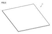
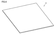
- the conductive slurry is formed by a doctor blade method, and two conductive sheets are produced as shown in FIGS. 5 and 6 so that the thickness after firing is preferably 1 to 40 ⁇ m. .
- FIG. 5 shows the first conductive sheet 11.
- FIG. 6 shows the second conductive sheet 12.
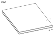
- the piezoelectric ceramic sheet 10 is sandwiched between the first conductive sheet 11 and the second conductive sheet 12 to obtain a laminated body in which these three layers are overlapped.
- This laminate is fired.
- the fired laminate is cut into a desired shape.
- a co-sintered body 15 as shown in FIGS. 8 and 9 is obtained.
- the co-sintered body 15 is produced, for example, so as to be a 40 mm ⁇ 10 mm rectangle when viewed in plan.
- FIG. 9 is a cross-sectional view of the co-sintered body 15 shown in FIG.
- the first conductor layer 16 is formed on the first surface 41 of the ferroelectric body 1
- the second conductor layer 17 is formed on the second surface 42.
- patterning is performed on the first conductor portion layer 16 using a photolithography technique.
- a photoresist is applied to the surface of the first conductor layer 16 and then pre-baked.
- a mask having a predetermined pattern is arranged on the upper side, and exposed by irradiating with ultraviolet rays. Transcript to.
- a pure water is immersed in an etching solution such as a ferric chloride solution to perform wet etching.
- the developed photoresist is stripped using a stripping solution.
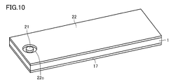
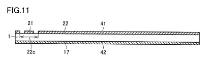
- the first conductor layer 16 is divided into two parts, and the first electrode 21 and the second electrode 22 are formed as shown in FIG. A cross-sectional view of this state is shown in FIG.
- the insulating film 5 is formed so as to cover the first electrode 21 and the second electrode 22.
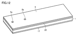
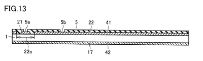
- a portion where the ferroelectric layer 1 is exposed in the opening 22 c of the second electrode 22 is also covered with the insulating film 5.
- openings 5a and 5b are formed in the insulating film 5 so that a part of the first electrode 21 and a part of the second electrode 22 are exposed.
- a cross-sectional view of this state is shown in FIG.
- an insulating solution containing a photosensitive insulating material such as a photosensitive epoxy resin is prepared.
- This insulating solution is applied by a coating method such as spin coating. Then, it prebakes, exposes through a mask of a predetermined pattern, and develops. Furthermore, the insulating film 5 having the openings 5a and 5b can be obtained by post baking.
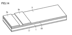
- extraction electrodes 3a and 3b are formed. That is, first, a conductive layer is formed by applying a thin film forming method such as a sputtering method to the surface of the laminate on which the insulating film 5 is formed. Thereafter, extraction electrodes 3a and 3b are formed on the conductive layer by the above-described photolithography technique as shown in FIG. A cross-sectional view of this state is shown in FIG.
- the second conductor layer 17 is divided into two.
- the third electrode 23 and the fourth electrode 24 are formed.
- the extraction electrodes 3a and 3b are electrically connected by an appropriate method. If the signal generated from the sensor unit is to be applied to the memory unit with an alternating current, a low-resistance resistor chip may be mounted to extend between the extraction electrodes 3a and 3b for this connection. Thus, the piezoelectric device 101 as shown in FIGS. 1 and 2 can be obtained.
- the connection means between the extraction electrodes 3 a and 3 b is schematically shown as the wiring 25.
- the extraction electrodes 3a and 3b are formed as separate electrodes when the extraction electrodes 3a and 3b are formed.
- the electrodes may be formed as a connected integral electrode.
- various electrode processing using a photolithography technique is performed after the fired laminated body is cut into a desired shape.
- the process from electrode processing to connection is further maintained in a large format without cutting the fired laminated body. It is good also as performing after that and cutting into a desired shape. In this case, the manufacturing cost can be reduced.
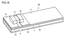
- FIG. 18 A piezoelectric device 102 in the present embodiment is shown in FIG.
- FIG. 19 A cross-sectional view of the piezoelectric device 102 is shown in FIG.
- the extraction electrodes 3a and 3b are connected by the wiring 25.
- the extraction electrodes 3a and 3b are connected by the diode 31. ing.
- the diode 31 has a chip shape.
- the first electrode 21 and the second electrode 22 are electrically connected to each other via a diode 31.
- the AC signal generated from the sensor unit is rectified by the diode 31 and applied to the memory unit.
- FIG. 21 is a cross-sectional view taken along the line XXI-XXI in FIG.
- the piezoelectric device 103 includes a substrate 32.
- a first pad electrode 33 and a second pad electrode 34 are disposed on the surface of the substrate 32.
- the first pad electrode 33 is electrically connected to the third electrode 23
- the second pad electrode 34 is electrically connected to the fourth electrode 24, and the first pad electrode 33 and the second pad electrode 34 can be switched to each other for electrical connection.
- a switch 35 is disposed between the first pad electrode 33 and the second pad electrode 34.
- the switch 35 By operating the switch 35, the presence / absence of electrical connection between the first pad electrode 33 and the second pad electrode 34 can be switched.
- a portion protruding like a cantilever from the substrate 32 causes vibration when an impact is applied to the entire piezoelectric device 103.
- the vibration generated in this portion is converted into an electric signal by the sensor unit in the ferroelectric layer 1.
- This electric signal is rectified by the diode 31, becomes a potential difference between the first electrode 21 and the third electrode 23, and is input to the memory unit in the ferroelectric layer 1.
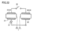
- FIG. 22 is a circuit diagram of the piezoelectric device 103 according to the present embodiment.
- the piezoelectric device 103 includes a sensor unit 51 and a memory unit 52.
- the thickness of the piezoelectric film was 15 ⁇ m, and the thickness of each of the first conductor layer 16 and the second conductor layer 17 was about 2 ⁇ m.
- a constant voltage is applied between the second electrode 22 and the second pad electrode 34 of the piezoelectric device 103 to polarize the region corresponding to the sensor portion in the ferroelectric layer 1.
- the switch 35 turned on, the impact was artificially applied by hitting the impact sensor portion with the handle portion of the tweezers. Due to this impact, a potential difference was generated between the first electrode 21 and the third electrode 23.
- Several impacts were applied, and as a result, a potential difference of about 1 to 20 V was detected depending on the magnitude of the applied impact.
- the piezoelectric device 103 produced by the inventor was connected to a Soya tower circuit with the switch 35 turned off, and a hysteresis loop between the first electrode 21 and the third electrode 23 was measured.
- the positive and negative voltages are defined assuming that the electrical signal generated when the impact is applied is rectified in the negative direction by the diode 31, the voltage sweep during the hysteresis measurement was performed in the order of 0 ⁇ negative ⁇ positive ⁇ 0.
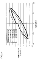
- the potential difference generated between the second electrode 22 and the fourth electrode 24 is large when an impact is applied, the hysteresis shape before and after the impact application is greatly different as shown in FIG.
- the potential difference generated between the second electrode 22 and the fourth electrode 24 is small, as shown in FIG. 24, no difference was found in the hysteresis shape before and after the impact application.
- the case where the sensor portion has a unimorph structure is illustrated, but it is not necessarily limited to the unimorph structure.
- a multimorph structure may be used as long as the total thickness of the ferroelectric layer 1 is 100 ⁇ m or less.
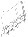
- FIG. 25 shows the piezoelectric device 104 in the present embodiment.
- the piezoelectric device 104 includes a plurality of memory units.
- the piezoelectric device 104 includes a total of n memory units from 1 to n.
- the piezoelectric device 104 includes n sensor units corresponding to the n memory units.
- the ferroelectric layer 1 may be a single layer in common across n memory units and n sensor units.
- the insulating film 5 may be collectively formed as a single film.
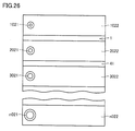
- FIG. 26 shows a view from the upper side in FIG. 25 with the insulating film 5 and the like removed from the piezoelectric device 104.
- the first surface 41 side of the ferroelectric layer 1 is visible.
- the first surface 41 of the ferroelectric layer 1 has the first first electrode 1021, the first second electrode 1022, the second first electrode 2021, the second second electrode 2022, the third The first electrode 3021, the third second electrode 3022,..., The n-th first electrode n 021, and the n-th second electrode n 022 are arranged apart from each other.
- the first first electrode 1021 is formed in an island shape while being surrounded by the first second electrode 1022.
- the second first electrode 2021 is formed in an island shape in a state surrounded by the second second electrode 2022.
- the n-th first electrode n021 is formed in an island shape while being surrounded by the n-th second electrode n022.
- the first first electrode 1021, the second first electrode 2021, the third first electrode 3021,..., And the nth first electrode n021 are all circular and have different diameters. When any two electrodes are taken out from the first first electrode 1021, the second first electrode 2021, the third first electrode 3021,... The electrodes have different areas.
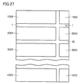
- FIG. 27 shows the piezoelectric device 104 viewed from the lower side in FIG. Since this corresponds to the inverted state compared to FIG. 26, the left end in FIG. 26 is the right end in FIG. In FIG. 27, the second surface 42 side of the ferroelectric layer 1 is visible.
- the first surface 42 of the ferroelectric layer 1 has a first third electrode 1023, a first fourth electrode 1024, a second third electrode 2023, a second fourth electrode 2024, a third The third electrode 3023, the third fourth electrode 3024,..., The n-th third electrode n023, and the n-th fourth electrode n024 are arranged separately from each other.
- the first third electrode 1023, the second third electrode 2023,..., The nth third electrode n023 may have the same shape.
- the first fourth electrode 1024, the second fourth electrode 2024,..., The nth fourth electrode n024 may all have the same shape.
- the piezoelectric device 104 in the present embodiment is a piezoelectric device, and includes a ferroelectric layer 1 having a first surface 41 and a second surface 42 facing opposite sides when n is an integer of 2 or more. Further, the piezoelectric device 104 includes, for each of the integers k from 1 to n, the k-th first electrode formed of the sintered metal on the first surface 41 and the first electrode formed of the sintered metal on the first surface 41.
- the third electrode includes a region facing the kth first electrode with the ferroelectric layer 1 interposed therebetween, and the kth fourth electrode is stronger than at least a part of the kth second electrode. It includes regions that face each other across the dielectric layer 1.
- the first first electrode, the second first electrode, the third first electrode, ..., the n-th first electrode, the first second electrode, the second second electrode, the third second electrode The n-th second electrodes are spaced apart from each other and are disposed in different regions.
- the nth fourth electrodes are spaced apart from each other and arranged in different regions.
- the k1st electrode and the k2 first electrode have different areas.
- n memory units and n sensor units are configured in one piezoelectric device.
- electric charges are generated in each of the n sensor units. This electric charge causes a potential difference between the first electrode and the third electrode in the corresponding memory unit.
- the n memory units have different areas of the first electrode, and thus the voltages applied to the memory units are different. Since the voltage applied to each memory unit is different, a plurality of memory units may include a series circuit capable of polarization reversal and a series circuit capable of polarization reversal. By confirming the presence or absence of polarization reversal for each memory unit later, the magnitude of the impact applied to the piezoelectric device can be quantitatively confirmed.
- the ferroelectric layer 1 may have a thickness of 1 ⁇ m to 100 ⁇ m.
- the k-th first electrode is circular, and the k-th second electrode is arranged to surround the k-th first electrode. May have been.
- this configuration it is easy to adjust the area of the first electrode.
- the fact that the ferroelectric layer 1 is covered with any electrode means that in this region, the brittle ceramic is covered with a malleable metal and the mechanical strength of the ferroelectric layer 1 is reinforced.
- the k-th second electrode is arranged so as to surround the k-th first electrode, the region reinforced in this way can be enlarged, Therefore, the risk of damaging the ferroelectric layer 1 during electrode processing can be reduced.
- the kth first electrode and the kth second electrode may be electrically connected to each other via a diode 31.
- the AC signal generated from each sensor unit is rectified by the diode 31 and applied to the corresponding memory unit.
- FIG. 28 shows the piezoelectric device 105 in the present embodiment.
- FIG. 29 shows a state in which some elements such as the insulating film 5 are removed from FIG.
- the piezoelectric device 105 in the present embodiment is a piezoelectric device, and includes the ferroelectric layer 1 having a first surface 41 and a second surface 42 that face opposite sides. Further, the piezoelectric device 105 includes a first first electrode 1021 formed of a sintered metal on the first surface 41, a first second electrode 1022 formed of a sintered metal on the first surface 41, and a second surface. 42 includes a first third electrode 1023 formed of sintered metal and a first fourth electrode formed of sintered metal on the second surface 42. The first third electrode 1023 includes the first first electrode The first and second electrodes are opposed to at least a part of the first and second electrodes 1022 with the ferroelectric layer 1 interposed therebetween. Includes area.
- the piezoelectric device 105 includes a second first electrode 2021 formed of sintered metal on the first surface 41, a second second electrode 2022 formed of sintered metal on the first surface 41, and a second surface.
- 42 includes a second third electrode 2023 formed of sintered metal, and a second fourth electrode 2024 formed of sintered metal on the second surface 42.
- the second third electrode 2023 includes a region facing the second first electrode 2021 with the ferroelectric layer 1 interposed therebetween.
- the second fourth electrode 2024 includes a region facing at least a part of the second second electrode 2022 with the ferroelectric layer 1 interposed therebetween.
- the first first electrode 1021, the second first electrode 2021, the first second electrode 1022, and the second second electrode 2022 are spaced apart from each other and disposed in different regions.
- the first third electrode 1023, the second third electrode 2023, the first fourth electrode, and the second fourth electrode 2024 are spaced apart from each other and disposed in different regions.
- the first first electrode 1021 and the second first electrode 2021 have different areas.
- the first first pad electrode 1033 is connected to the first third electrode 1023.
- the first second pad electrode 1034 is connected to a first fourth electrode (not shown).
- the second first pad electrode 2033 is connected to the second third electrode 2023.
- the second second pad electrode 2034 is connected to the second fourth electrode 2024.
- two memory units and two sensor units are configured in one piezoelectric device 105.
- the first first electrode 1021 and the second first electrode 2021 have different areas, when one impact is applied to the piezoelectric device, the voltages applied to the two memory units. Will be different.
- polarization inversion occurs in two memory units, polarization inversion occurs in only one memory unit, or polarization inversion does not occur in two memory units 3 It is possible to identify the magnitude of the impact applied to the piezoelectric device 105 by examining later which one of these states is possible.
Landscapes
- Engineering & Computer Science (AREA)
- Physics & Mathematics (AREA)
- General Physics & Mathematics (AREA)
- Computer Hardware Design (AREA)
- Power Engineering (AREA)
- Chemical & Material Sciences (AREA)
- Ceramic Engineering (AREA)
- Semiconductor Memories (AREA)
- General Electrical Machinery Utilizing Piezoelectricity, Electrostriction Or Magnetostriction (AREA)
Abstract
圧電デバイス(101)は、第1面(41)および第2面(42)を有する強誘電体層(1)と、第1面(41)の一部を覆い、焼結金属によって形成された第1電極(21)と、第1電極(21)から離隔しつつ第1面(41)の第1電極(21)に覆われていない領域のうちの一部を覆い、焼結金属によって形成された第2電極(22)と、第2面(42)のうち第1電極(21)に対向する領域を含むように第2面(42)の一部を覆い、焼結金属によって形成された第3電極(23)と、第3電極(23)から離隔しつつ第2面(42)の第3電極(23)に覆われていない領域のうちの一部を覆う第4電極(24)とを備え、第4電極(24)は、第2電極(22)の少なくとも一部に対して強誘電体層(1)を挟んで対向している。
Description
本発明は、圧電デバイスに関し、特に衝撃センサとして使用可能な圧電デバイスに関するものである。
特開2013-96931号公報(特許文献1)には、「衝撃検知・記録装置」と称して、無電源でありながら加わった衝撃を検知し、記録することができる装置が記載されている。特許文献1では、この装置を得るために、衝撃センサと強誘電体メモリとをそれぞれ別々に作製し、その後、両者の電極を導電性接着剤により接合することで一体化している。衝撃センサは、一般的に所望の厚さに成形した圧電セラミック板に対して電極を形成するなどして作製される。一方、強誘電体メモリは、Siウェハー上に薄膜プロセスを用いて成膜、パターニングすることで作製されている。
したがって、特許文献1の装置を実際に作製する際には、焼結した圧電セラミック板の加工を主とする衝撃センサの製造工程と、薄膜プロセスを主とする強誘電体メモリの製造工程と、両者を電気的にも機械的にも接合させる一体化の工程とを実施する必要がある。
特開2007-329393号公報(特許文献2)には、センサと強誘電体メモリとが混載された半導体装置が記載されている。
特許文献1に記載されるような衝撃センサに用いられる圧電体は、強誘電体でもあるので、この圧電体の分極反転を利用した強誘電体メモリを作製すれば、上述の工程を大幅に短縮できる可能性がある。しかし、衝撃センサで用いられている圧電体の厚みは100μm以上であり、この厚みの圧電体を分極反転させるのに必要な電圧は100V以上と見積もられる。強誘電体メモリの両端子間に発生する電極が100V、特に40Vを超える高電圧になると、周辺回路を高電圧に耐えられるようにする必要があり、信頼性設計に多大な労力が必要となる。一方で、衝撃センサで用いられる圧電体を加工して10V程度で分極反転可能になるまで薄くしようとすると、圧電体の厚みは20μm以下とする必要がある。こうなると、圧電体を薄くするための処理を含めた素子の製造過程で圧電体自体が破損してしまう可能性が高く、実際上のハンドリングに素子が耐えられない。
以上のように、製造工程の簡略化のために、衝撃センサで用いられる圧電体と強誘電体メモリで用いられる強誘電体とを共通化しようとしても、信頼性設計や製造工程が難しくなってしまい、実施が不可能であった。
特許文献2では、圧力センサと強誘電体メモリを共に薄膜プロセスで作製していることから、特許文献1で懸念された製造工程の煩雑さは解消されると期待される。一方で、強誘電体メモリを分極反転させる程度の電荷を発生する圧力センサを作製するには、圧電体の寸法に関する制約条件が発生し、この条件をクリアする厚みの圧力センサを薄膜プロセスで作製しようとすると、多大な労力を必要とすることになる。
そこで、本発明は、低い電圧で分極反転可能な強誘電体メモリを備え、ハンドリング可能な程度の厚みを有し、簡便に作製可能な圧電デバイスを提供することを目的とする。
上記目的を達成するため、本発明の第1の局面に基づく圧電デバイスは、互いに逆の側を向く第1面および第2面を有する強誘電体層と、上記第1面の一部を覆い、焼結金属によって形成された第1電極と、上記第1電極から離隔しつつ上記第1面の上記第1電極に覆われていない領域のうちの一部を覆い、焼結金属によって形成された第2電極と、上記第2面のうち上記第1電極に対向する領域を含むように上記第2面の一部を覆い、焼結金属によって形成された第3電極と、上記第3電極から離隔しつつ上記第2面の上記第3電極に覆われていない領域のうちの一部を覆い、焼結金属によって形成された第4電極とを備える。上記第4電極は、上記第2電極の少なくとも一部に対して上記強誘電体層を挟んで対向している。
上記発明において好ましくは、上記強誘電体層は、厚みが1μm以上100μm以下である。
上記発明において好ましくは、上記第1電極は円形であり、上記第2電極は上記第1電極を取り囲むように配置されている。
上記発明において好ましくは、上記第1電極と上記第2電極とは、ダイオードを介して互いに電気的に接続されている。
上記発明において好ましくは、上記第3電極には第1パッド電極が電気的に接続されており、上記第4電極には第2パッド電極が電気的に接続されており、上記第1パッド電極と上記第2パッド電極とは互いに電気的接続の有無が切替え可能である。
上記発明において好ましくは、上記第1電極および上記第2電極の少なくとも一部を覆う絶縁膜を備える。
上記目的を達成するため、本発明の第2の局面に基づく圧電デバイスは、圧電デバイスであって、nを2以上の整数とすると、互いに逆の側を向く第1面および第2面を有する強誘電体層を備え、さらに、上記圧電デバイスは、1からnまでの整数kの各々について、上記第1面に焼結金属によって形成された第k第1電極と、上記第1面に焼結金属によって形成された第k第2電極と、上記第2面に焼結金属によって形成された第k第3電極と、上記第2面に焼結金属によって形成された第k第4電極とを有し、上記第k第3電極は、上記第k第1電極に対して上記強誘電体層を挟んで対向する領域を含み、上記第k第4電極は、上記第k第2電極の少なくとも一部に対して上記強誘電体層を挟んで対向する領域を含み、上記第1第1電極、上記第2第1電極、上記第3第1電極、…、上記第n第1電極、上記第1第2電極、上記第2第2電極、上記第3第2電極、…、上記第n第2電極は、互いに離隔し、互いに異なる領域に配置されており、上記第1第3電極、上記第2第3電極、上記第3第3電極、…、上記第n第3電極、上記第1第4電極、上記第2第4電極、上記第3第4電極、…、上記第n第4電極は、互いに離隔し、互いに異なる領域に配置されており、1からnまでの整数の中から任意に選択される互いに異なる2つの整数k1,k2について、上記第k1第1電極と上記第k2第1電極とは、面積が異なっている。
上記発明において好ましくは、上記強誘電体層は、厚みが1μm以上100μm以下である。
上記発明において好ましくは、1からnまでの整数kの各々について、上記第k第1電極は円形であり、上記第k第2電極は上記第k第1電極を取り囲むように配置されている。
上記発明において好ましくは、1からnまでの整数kの各々について、上記第k第1電極と上記第k第2電極とは、ダイオードを介して互いに電気的に接続されている。
本発明によれば、1つの強誘電体層1の異なる部位を以てメモリ部とセンサ部とが形成されるので、組立時にメモリとセンサとを個別に用意する必要がなく、低い電圧で分極反転可能な強誘電体メモリを備え、ハンドリング可能な程度の厚みを有し、簡便に作製可能な圧電デバイスを実現することができる。
図面において示す寸法比は、必ずしも忠実に現実のとおりを表しているとは限らず、説明の便宜のために寸法比を誇張して示している場合がある。以下の説明において、上または下の概念に言及する際には、絶対的な上または下を意味するものではなく、図示された姿勢の中での相対的な上または下を意味するものである。
(実施の形態1)
図1~図3を参照して、本発明に基づく実施の形態1における圧電デバイスについて説明する。本実施の形態における圧電デバイス101の斜視図を図1に示す。図1におけるII-II線に関する矢視断面図を図2に示す。
図1~図3を参照して、本発明に基づく実施の形態1における圧電デバイスについて説明する。本実施の形態における圧電デバイス101の斜視図を図1に示す。図1におけるII-II線に関する矢視断面図を図2に示す。
本実施の形態における圧電デバイス101は、互いに逆の側を向く第1面41および第2面42を有する強誘電体層1と、第1面41の一部を覆い、焼結金属によって形成された第1電極21と、第1電極21から離隔しつつ第1面41の第1電極21に覆われていない領域のうちの一部を覆い、焼結金属によって形成された第2電極22と、第2面42のうち第1電極21に対向する領域を含むように第2面42の一部を覆い、焼結金属によって形成された第3電極23と、第3電極23から離隔しつつ第2面42の第3電極23に覆われていない領域のうちの一部を覆い、焼結金属によって形成された第4電極24とを備える。第4電極24は、第2電極22の少なくとも一部に対して強誘電体層1を挟んで対向している。
圧電デバイス101は、第1電極21および第2電極22を覆うように絶縁膜5を備えている。圧電デバイス101は、絶縁膜5の一部を覆うように、引出し電極3a,3bを備える。引出し電極3a,3bは、互いに離隔して設けられているが、配線25によって互いに電気的に接続されている。図1から引出し電極3a,3b、配線25および絶縁膜5を取り去った状態を図3に示す。第2電極22は開口部22cを有する。第1電極21は、開口部22cの内部に配置されている。第1電極21は、円形状であって、開口部22cに対して同心円状に配置されている。第1電極21は、第2電極22から離隔している。第4電極24は、間隙6を介して第3電極23から離隔している。なお、第1電極21は、円形状に限られるものではなく、たとえば楕円形状や多角形状であってもよい。
強誘電体層1は、国際公開第2015/166914号(特許文献3)に記載された技術に従って形成することができる。この技術に従えば、厚みが100μm以下である強誘電体層1を作製することができる。強誘電体層1は焼成によって得ることができる。
第1電極21、第2電極22、第3電極23、第4電極24も焼成によって得ることができる。強誘電体層1、第1電極21、第2電極22、第3電極23、第4電極24は、材料を積層した状態で一括して焼成することによって、これらの各部分を焼結体として同時に作製することができる。
本実施の形態における圧電デバイス101では、同一の強誘電体層1が強誘電体メモリと衝撃センサとの両方を兼ねる構造となっている。1つの強誘電体層1のうち第1電極21の投影領域内にある部分が強誘電体メモリとして働いている。この部分を以下「メモリ部」という。一方、強誘電体層1のうち第2電極22と第4電極24とによって挟まれている領域にある部分が衝撃センサとして働いている。この部分を以下「センサ部」という。本実施の形態では、このように1つの強誘電体層1の異なる部位を以てメモリ部とセンサ部とが形成されるので、組立時にメモリとセンサとを個別に用意する必要がない。したがって、本実施の形態における圧電デバイスは、メモリ部とセンサ部とを電気的、機械的に接続する工程を経ることなく作製することができる。接続する工程が不要であるということは、接続部に関する信頼性の問題も回避することができる。薄い焼結体によってメモリ部分とセンサ部分との両方を実現することができるので、特許文献1の技術に比べて圧電デバイスの低背化を図ることができる。本実施の形態によれば、低い電圧で分極反転可能な強誘電体メモリを備え、ハンドリング可能な程度の厚みを有し、簡便に作製可能な、衝撃センサとして使用可能な圧電デバイスを実現することができる。
本実施の形態における圧電デバイス101は、強誘電体層1の一部がセンサ部となっており、このセンサ部で衝撃時に発生する電荷を以て、メモリ部に情報の書き込みを行なうことができるので、外部から電源を供給する必要がなく、衝撃を自ら検知し、記録することができる。
特許文献2で本実施の形態と同様の構成を実現するには、塗布工程、乾燥工程、脱脂熱処理工程を何回も繰り返す必要があるが、本実施の形態では、厚み1μm程度のシートを用意し、これらを積層、焼成することで所望厚みの強誘電体を作製することができ、製造方法を大幅に簡略化することができる。
本実施の形態では、衝撃センサ部がユニモルフ構造であるものとして説明したが、ユニモルフ構造に限らない。圧電デバイスの総厚みが100μm以下であればよく、マルチモルフ構造であってもよい。
強誘電体層1は、厚みが1μm以上100μm以下であることが好ましい。この構成を採用することにより、強誘電体メモリと衝撃センサとの両方を兼ねる強誘電体層1を上述の方法で焼成により作製することができる。
本実施の形態で示したように、第1電極21は円形状であり、第2電極22は第1電極21を取り囲むように配置されていることが好ましい。この構成を採用することにより、第1電極21の面積を直径により一義的に決定することができる。また、この構成を採用することにより、強誘電体層1のうち第1電極21および第2電極22のいずれにも覆われていない領域を小さくすることが可能となる。強誘電体層1がいずれかの電極で覆われているということは、当該領域においては、脆性をもつセラミックが展性をもつ金属で覆われて強誘電体層1の機械的強度が補強されているということに他ならないところであるが、第2電極22が第1電極21を取り囲むように配置することとすれば、このように補強されている領域を大きくすることができるので、発生する応力が緩和され、電極加工時に強誘電体層1が破損するリスクを低減することができる。
第1電極21および第2電極22の少なくとも一部を覆う絶縁膜5を備えることが好ましい。この構成を採用することにより、第1電極21および第2電極22の少なくとも一部が絶縁膜5によって覆われるので、不所望な短絡が生じる確率を減らすことができる。
(製造方法)
本実施の形態における圧電デバイスの具体的な製造方法について説明する。
本実施の形態における圧電デバイスの具体的な製造方法について説明する。
まず、セラミック素原料を用意する。たとえば、強誘電体層1となるべき圧電セラミック基体をニオブ酸アルカリ系化合物で形成する場合、K化合物、Na化合物、Li化合物、Nb化合物などを用意する。あるいは、強誘電体層1となるべき圧電セラミック基体をPZT系化合物で形成する場合は、Pb化合物、Ti化合物、Zr化合物などを用意し、必要に応じて各種添加物を用意する。
次に、所定の配合モル比となるようにセラミック素原料を秤量する。この秤量物をPSZボールなどの粉砕媒体が内部に配置されたポットミルに投入する。溶媒の存在下で所定時間にわたってポットミルを回転させる。こうして、セラミック素原料を湿式で十分に混合粉砕する。さらに粉砕物を乾燥させた後、仮焼処理を行なうことによって、セラミック原料粉末を得る。
このセラミック原料粉末を解砕した後、有機バインダ、有機溶剤、分散剤、可塑剤を先ほどの粉砕媒体と共に、再びポットミルに投入し、このポットミルを回転させながら十分に湿式で混合粉砕することによって、セラミックスラリーを得る。
ドクターブレード法によってセラミックスラリーを成形加工し、焼成後の厚みが、好ましくは100μm以下となるように、圧電セラミックシートを作製する。圧電セラミックシート10を図4に示す。ここでは、圧電セラミックシート10が正方形であるものとして例示しているが、圧電セラミックシート10の形状はこれに限らない。
同様に、Ni、Cuなどの導電性材料を用意する。この導電性材料を有機バインダ、有機溶剤、分散剤、可塑剤と共に、粉砕媒体が内部に配置されたポットミルに投入し、ポットミルを回転させながら湿式で十分に湿式混合する。こうして、導電性スラリーを作製する。次いで、ドクターブレード法により、導電性スラリーを成形加工し、焼成後の厚みが、好ましくは1~40μmとなるように、図5および図6に示すように、2枚の導電性シートを作製する。図5に第1導電性シート11を示す。図6に第2導電性シート12を示す。
図7に示すように、圧電セラミックシート10を第1導電性シート11および第2導電性シート12によって挟み込むことによって、これら3層が重なった積層体を得る。この積層体を焼成する。焼成された積層体を所望の形状に切り分ける。こうして図8および図9に示すような共焼結体15を得る。共焼結体15は、たとえば平面的に見て40mm×10mmの長方形となるように作製される。図9は図8に示す共焼結体15の断面図である。共焼結体15においては、強誘電体1の第1面41に第1導体層16が形成され、第2面42に第2導体層17が形成されている。
次に、フォトリソグラフィ技術を使用して第1導体部層16にパターニング処理を施す。このパターニング処理においては、第1導体層16の表面にフォトレジストを塗布した後、プリベークし、その後、所定パターンを有するマスクを上方に配し、紫外線を照射して露光し、マスクパターンをフォトレジストに転写する。次いで、これを現像した後、純水で洗浄する。その後、これを塩化第二鉄溶液などのエッチング液に浸漬してウェットエッチングを行なう。現像されたフォトレジストを剥離溶液を使用して剥離する。このようなパターニング処理を行なった結果、第1導体層16は2つの部分に分かれ、図10に示すように、第1電極21および第2電極22が形成される。この状態の断面図を図11に示す。
次に、第1電極21および第2電極22を覆うように絶縁膜5を形成する。第2電極22の開口部22c内において強誘電体層1が露出している部分も絶縁膜5によって覆われる。ただし、第1電極21の一部および第2電極22の一部がそれぞれ露出するように、図12に示すように、絶縁膜5に開口部5a,5bを形成する。この状態の断面図を図13に示す。
絶縁膜5の形成のためには、たとえば、感光性エポキシ樹脂などの感光性絶縁性材料を含有した絶縁性溶液を用意する。スピンコート法などの塗布方法により、この絶縁性溶液を塗布する。その後、プリベークし、所定パターンのマスクを介して露光し、現像する。さらに、これをポストベークすることによって、開口部5a,5bを有する絶縁膜5を得ることができる。
次に、引出し電極3a,3bを形成する。すなわち、まず、絶縁膜5が形成された積層体の表面にスパッタリング法などの薄膜形成方法を適用して導電層を形成する。その後、この導電層に対して、上述したフォトリソグラフィ技術により、図14に示すように引出し電極3a,3bを形成する。この状態の断面図を図15に示す。
次に、フォトリソグラフィ技術により第2導体層17にパターニング処理を施す。これにより、第2導体層17が2つに分割される。こうして、図16および図17に示したように、第3電極23と第4電極24とが形成される。
次に、引出し電極3a,3b間を適当な方法で電気的に接続する。センサ部から発生する信号を交流のままメモリ部に印加すべきであれば、この接続のためには、引出し電極3a,3b間にまたがるように低抵抗の抵抗チップを実装してもよい。こうして、図1および図2に示すような圧電デバイス101を得ることができる。ここでは、引出し電極3a,3b間の接続手段については、配線25として模式的に示している。
信号を交流のままメモリ部に印加してよい場合、引出し電極3a,3bを配線25によって接続する代わりに、引出し電極3a,3bを作製する際に引出し電極3a,3bを別々の電極として形成するのではなくつながった一体的な電極として形成してもよい。
なお、ここでは、焼成した積層体を所望の形状に切り分けた後にフォトリソグラフィ技術を用いた各種電極加工を行なっているが、焼成した積層体を切り分けずに大判のままさらに電極加工から接続までを行ない、その後で所望の形状に切り分けることとしてもよい。この場合、製造コストの低減を図ることができる。
(実施の形態2)
図18および図19を参照して、本発明に基づく実施の形態2における圧電デバイスについて説明する。本実施の形態における圧電デバイス102を図18に示す。圧電デバイス102の断面図を図19に示す。
図18および図19を参照して、本発明に基づく実施の形態2における圧電デバイスについて説明する。本実施の形態における圧電デバイス102を図18に示す。圧電デバイス102の断面図を図19に示す。
実施の形態1で説明した圧電デバイス101では、引出し電極3a,3b間を配線25によって接続していたが、本実施の形態における圧電デバイス102では、引出し電極3a,3b間はダイオード31で接続されている。ダイオード31はチップ形状のものである。圧電デバイス102においては、第1電極21と第2電極22とは、ダイオード31を介して互いに電気的に接続されている。
本実施の形態では、第1電極21と第2電極22とがダイオード31を介して接続されているので、センサ部から発生した交流信号はダイオード31によって整流された状態で、メモリ部に印加される。
(実施の形態3)
図20~図22を参照して、本発明に基づく実施の形態3における圧電デバイスについて説明する。本実施の形態における圧電デバイス103を図20に示す。図20におけるXXI-XXI線に関する矢視断面図を図21に示す。圧電デバイス103は、基板32を備えている。基板32の表面には、第1パッド電極33と、第2パッド電極34とが配置されている。圧電デバイス103においては、第3電極23には第1パッド電極33が電気的に接続されており、第4電極24には第2パッド電極34が電気的に接続されており、第1パッド電極33と第2パッド電極34とは互いに電気的接続の有無が切替え可能である。
図20~図22を参照して、本発明に基づく実施の形態3における圧電デバイスについて説明する。本実施の形態における圧電デバイス103を図20に示す。図20におけるXXI-XXI線に関する矢視断面図を図21に示す。圧電デバイス103は、基板32を備えている。基板32の表面には、第1パッド電極33と、第2パッド電極34とが配置されている。圧電デバイス103においては、第3電極23には第1パッド電極33が電気的に接続されており、第4電極24には第2パッド電極34が電気的に接続されており、第1パッド電極33と第2パッド電極34とは互いに電気的接続の有無が切替え可能である。
図20に示すように、第1パッド電極33と第2パッド電極34との間にはスイッチ35が配置されている。スイッチ35を操作することによって、第1パッド電極33と第2パッド電極34との間の電気的接続の有無を切り替えることができる。圧電デバイス103において、基板32から片持ち梁のように張り出している部分は、圧電デバイス103全体に衝撃が加わった際に振動を引き起こす。この部分で発生する振動が、強誘電体層1のうちセンサ部によって電気信号に変換される。この電気信号がダイオード31によって整流されて、第1電極21と第3電極23との間の電位差となって、強誘電体層1のうちメモリ部に入力される。
本実施の形態における圧電デバイス103を回路図で示すと、図22のようになる。圧電デバイス103は、センサ部51と、メモリ部52とを備える。
発明者が作製した圧電デバイス103では、圧電膜の厚さは15μm、第1導体層16および第2導体層17の厚みはそれぞれ約2μmであった。圧電デバイス103の第2電極22と第2パッド電極34との間に一定の電圧を印加し、強誘電体層1のうちセンサ部に相当する領域を分極する。その後で、スイッチ35をONとした状態で、ピンセットの柄の部分で衝撃センサ部を叩くことで衝撃を人為的に印加した。この衝撃により、第1電極21と第3電極23との間に電位差が発生した。いくとおりかの大きさの衝撃を加えたが、その結果、与える衝撃の大きさに応じて1~20V程度の電位差が検出された。
発明者が作製した圧電デバイス103を、スイッチ35をOFFとした状態で、ソーヤタワー回路に接続して、第1電極21と第3電極23との間のヒステリシスループを測定した。衝撃印加時に発生した電気信号をダイオード31で負方向に整流しているものとして電圧の正負を定義すると、ヒステリシス測定の際の電圧の掃引は、0→負→正→0の順で行なった。その結果、衝撃を印加した際に第2電極22と第4電極24との間に発生する電位差が大きい場合には、図23に示すように、衝撃印加前後でのヒステリシス形状が大きく異なっていたのに対して、第2電極22と第4電極24との間に発生した電位差が小さい場合は、図24に示すように、衝撃印加前後でのヒステリシス形状に差異が見られなかった。
この実験からは、強い衝撃をセンサ部に印加することにより、大きな電位差を発生させ、その電位差を以てメモリ部の分極状態を変更できることが確認できた。
ここではセンサ部がユニモルフ構造である場合について例示したが、必ずしもユニモルフ構造に限定するものではない。強誘電体層1の総厚みが100μm以下であればマルチモルフ構造であってもよい。
(実施の形態4)
図25~図27を参照して、本発明に基づく実施の形態4における圧電デバイスについて説明する。本実施の形態における圧電デバイス104を図25に示す。圧電デバイス104は、複数のメモリ部を備える。図25に示した例では、圧電デバイス104は、第1から第nの合計n個のメモリ部を備えている。圧電デバイス104は、n個のメモリ部に対応してn個のセンサ部を備える。圧電デバイス104において、強誘電体層1は、n個のメモリ部およびn個のセンサ部にわたって共通して単一の層であってよい。絶縁膜5についても、同様に単一の膜として一括して形成されていてよい。
図25~図27を参照して、本発明に基づく実施の形態4における圧電デバイスについて説明する。本実施の形態における圧電デバイス104を図25に示す。圧電デバイス104は、複数のメモリ部を備える。図25に示した例では、圧電デバイス104は、第1から第nの合計n個のメモリ部を備えている。圧電デバイス104は、n個のメモリ部に対応してn個のセンサ部を備える。圧電デバイス104において、強誘電体層1は、n個のメモリ部およびn個のセンサ部にわたって共通して単一の層であってよい。絶縁膜5についても、同様に単一の膜として一括して形成されていてよい。
圧電デバイス104から絶縁膜5などを取り去った状態で図25における上側から見たところを図26に示す。図26では、強誘電体層1の第1面41側が見えている。図26に示すように、強誘電体層1の第1面41には、第1第1電極1021、第1第2電極1022、第2第1電極2021、第2第2電極2022、第3第1電極3021、第3第2電極3022、…、第n第1電極n021、第n第2電極n022がそれぞれ離隔した状態で配置されている。第1第1電極1021は、第1第2電極1022に取り囲まれた状態で、アイランド状に形成されている。第2第1電極2021は、第2第2電極2022に取り囲まれた状態で、アイランド状に形成されている。以下同様に続き、第n第1電極n021は、第n第2電極n022に取り囲まれた状態で、アイランド状に形成されている。第1第1電極1021、第2第1電極2021、第3第1電極3021、…、第n第1電極n021は、いずれも円形であり、それぞれ直径が異なっている。第1第1電極1021、第2第1電極2021、第3第1電極3021、…、第n第1電極n021の中からいずれか任意の2個の電極を取り出して注目すると、常に当該2個の電極は面積が異なっている。
圧電デバイス104を図25における下側から見たところを図27に示す。図26に比べて裏返した状態に相当するので、図26における左端は、図27においては右端となっている。図27では、強誘電体層1の第2面42側が見えている。図27に示すように、強誘電体層1の第1面42には、第1第3電極1023、第1第4電極1024、第2第3電極2023、第2第4電極2024、第3第3電極3023、第3第4電極3024、…、第n第3電極n023、第n第4電極n024がそれぞれ離隔した状態で配置されている。第1第3電極1023、第2第3電極2023、…、第n第3電極n023はいずれも同じ形状であってよい。第1第4電極1024、第2第4電極2024、…、第n第4電極n024はいずれも同じ形状であってよい。
以上述べた圧電デバイス104の構成を整理すると、以下のように表現することができる。
本実施の形態における圧電デバイス104は、圧電デバイスであって、nを2以上の整数とすると、互いに逆の側を向く第1面41および第2面42を有する強誘電体層1を備える。さらに、圧電デバイス104は、1からnまでの整数kの各々について、第1面41に焼結金属によって形成された第k第1電極と、第1面41に焼結金属によって形成された第k第2電極と、第2面42に焼結金属によって形成された第k第3電極と、第2面42に焼結金属によって形成された第k第4電極とを有し、前記第k第3電極は、前記第k第1電極に対して強誘電体層1を挟んで対向する領域を含み、前記第k第4電極は、前記第k第2電極の少なくとも一部に対して強誘電体層1を挟んで対向する領域を含む。前記第1第1電極、前記第2第1電極、前記第3第1電極、…、前記第n第1電極、前記第1第2電極、前記第2第2電極、前記第3第2電極、…、前記第n第2電極は、互いに離隔し、互いに異なる領域に配置されている。前記第1第3電極、前記第2第3電極、前記第3第3電極、…、前記第n第3電極、前記第1第4電極、前記第2第4電極、前記第3第4電極、…、前記第n第4電極は、互いに離隔し、互いに異なる領域に配置されている。1からnまでの整数の中から任意に選択される互いに異なる2つの整数k1,k2について、前記第k1第1電極と前記第k2第1電極とは、面積が異なっている。
本実施の形態では、1つの圧電デバイスの中にn個のメモリ部とn個のセンサ部が構成されている。1つの衝撃がこの圧電デバイスに加わったときにはn個のセンサ部の各々で、電荷が発生する。この電荷は、対応するメモリ部における第1電極と第3電極との間に電位差を生じさせることになる。各センサ部によってそれぞれ同等の電荷が発生している場合であっても、n個あるメモリ部は、それぞれ第1電極の面積が異なるので、各メモリ部に印加される電圧は異なる。各メモリ部ごとに印加される電圧が異なることにより、複数あるメモリ部の中には、分極反転が可能な直列回路と、分極反転が不可能な直列回路とが存在しうる。メモリ部ごとの分極反転の有無を後から確認することにより、この圧電デバイスに加わった衝撃の大きさを定量的に確認することができる。
本実施の形態では、強誘電体層1は、厚みが1μm以上100μm以下であってもよい。
本実施の形態で示したように、1からnまでの整数kの各々について、前記第k第1電極は円形であり、前記第k第2電極は前記第k第1電極を取り囲むように配置されていてよい。この構成を採用することにより、第1電極の面積を調整しやすい。また、この構成を採用することにより、強誘電体層1のうち第k第1電極および第k第2電極のいずれにも覆われていない領域を小さくすることが可能となる。強誘電体層1がいずれかの電極で覆われているということは、当該領域においては、脆性をもつセラミックが展性をもつ金属で覆われて強誘電体層1の機械的強度が補強されているということに他ならないところであるが、第k第2電極が第k第1電極を取り囲むように配置することとすれば、このように補強されている領域を大きくすることができるので、発生する応力が緩和され、電極加工時に強誘電体層1が破損するリスクを低減することができる。
図25に示すように、1からnまでの整数kの各々について、前記第k第1電極と前記第k第2電極とは、ダイオード31を介して互いに電気的に接続されていてもよい。この構成を採用することにより、各センサ部から発生した交流信号はダイオード31によって整流された状態で、対応するメモリ部に印加される。
(実施の形態5)
図28~図29を参照して、本発明に基づく実施の形態5における圧電デバイスについて説明する。本実施の形態における圧電デバイス105を図28に示す。本実施の形態における圧電デバイス105は、実施の形態4における圧電デバイス104においてn=2とし、さらにいくつかの部品を追加したものに相当する。図28から絶縁膜5などいくつかの要素を取り去った状態を図29に示す。
図28~図29を参照して、本発明に基づく実施の形態5における圧電デバイスについて説明する。本実施の形態における圧電デバイス105を図28に示す。本実施の形態における圧電デバイス105は、実施の形態4における圧電デバイス104においてn=2とし、さらにいくつかの部品を追加したものに相当する。図28から絶縁膜5などいくつかの要素を取り去った状態を図29に示す。
本実施の形態における圧電デバイス105は、圧電デバイスであって、互いに逆の側を向く第1面41および第2面42を有する強誘電体層1を備える。さらに、圧電デバイス105は、第1面41に焼結金属によって形成された第1第1電極1021と、第1面41に焼結金属によって形成された第1第2電極1022と、第2面42に焼結金属によって形成された第1第3電極1023と、第2面42に焼結金属によって形成された第1第4電極とを有し、第1第3電極1023は、第1第1電極1021に対して強誘電体層1を挟んで対向する領域を含み、第1第4電極は、第1第2電極1022の少なくとも一部に対して強誘電体層1を挟んで対向する領域を含む。さらに、圧電デバイス105は、第1面41に焼結金属によって形成された第2第1電極2021と、第1面41に焼結金属によって形成された第2第2電極2022と、第2面42に焼結金属によって形成された第2第3電極2023と、第2面42に焼結金属によって形成された第2第4電極2024とを有する。第2第3電極2023は、第2第1電極2021に対して強誘電体層1を挟んで対向する領域を含む。第2第4電極2024は、第2第2電極2022の少なくとも一部に対して強誘電体層1を挟んで対向する領域を含む。第1第1電極1021、第2第1電極2021、第1第2電極1022、第2第2電極2022は、互いに離隔し、互いに異なる領域に配置されている。第1第3電極1023、第2第3電極2023、前記第1第4電極、第2第4電極2024は、互いに離隔し、互いに異なる領域に配置されている。第1第1電極1021と第2第1電極2021とは、面積が異なっている。
図28に示すように、第1第1パッド電極1033が第1第3電極1023に接続されている。第1第2パッド電極1034は、図示されない第1第4電極に接続されている。第2第1パッド電極2033が第2第3電極2023に接続されている。第2第2パッド電極2034が第2第4電極2024に接続されている。
本実施の形態では、1つの圧電デバイス105の中に2個のメモリ部と2個のセンサ部が構成されている。本実施の形態では、第1第1電極1021と第2第1電極2021とで面積が異なっているので、1つの衝撃がこの圧電デバイスに加わったときには、2個のメモリ部に印加される電圧は異なったものとなる。圧電デバイス105に衝撃が加わったときに、2個のメモリ部とも分極反転が起こるか、1個のメモリ部のみで分極反転が起こるか、2個のメモリ部とも分極反転が起こらないかの3通りの状態がありえ、このいずれであるかを後から調べることにより、圧電デバイス105に加わった衝撃の大きさがどの程度であったかを識別することができる。
なお、上記実施の形態のうち複数を適宜組み合わせて採用してもよい。
なお、今回開示した上記実施の形態はすべての点で例示であって制限的なものではない。本発明の範囲は上記した説明ではなくて請求の範囲によって示され、請求の範囲と均等の意味および範囲内でのすべての変更を含むものである。
なお、今回開示した上記実施の形態はすべての点で例示であって制限的なものではない。本発明の範囲は上記した説明ではなくて請求の範囲によって示され、請求の範囲と均等の意味および範囲内でのすべての変更を含むものである。
1 強誘電体層、3a,3b 引出し電極、5 絶縁膜、5a,5b (絶縁膜の)開口部、6 間隙、10 圧電セラミックシート、11 第1導電性シート、12 第2導電性シート、15 共焼結体、16 第1導体層、17 第2導体層、21 第1電極、22 第2電極、22c (第2電極の)開口部、23 第3電極、24 第4電極、25 配線、31 ダイオード、32 基板、33 第1パッド電極、34 第2パッド電極、35 スイッチ、41 第1面、42 第2面、51 センサ部、52 メモリ部、101,102,103,104,105 圧電デバイス、1021 第1第1電極、1022 第1第2電極、1023 第1第3電極、1033 第1第1パッド電極、1034 第1第2パッド電極、2021 第2第1電極、2022 第2第2電極、2023 第2第3電極、2024 第2第4電極、2033 第2第1パッド電極、2034 第2第2パッド電極。
Claims (10)
- 互いに逆の側を向く第1面および第2面を有する強誘電体層と、
前記第1面の一部を覆い、焼結金属によって形成された第1電極と、
前記第1電極から離隔しつつ前記第1面の前記第1電極に覆われていない領域のうちの一部を覆い、焼結金属によって形成された第2電極と、
前記第2面のうち前記第1電極に対向する領域を含むように前記第2面の一部を覆い、焼結金属によって形成された第3電極と、
前記第3電極から離隔しつつ前記第2面の前記第3電極に覆われていない領域のうちの一部を覆い、焼結金属によって形成された第4電極とを備え、
前記第4電極は、前記第2電極の少なくとも一部に対して前記強誘電体層を挟んで対向している、圧電デバイス。 - 前記強誘電体層は、厚みが1μm以上100μm以下である、請求項1に記載の圧電デバイス。
- 前記第1電極は円形であり、前記第2電極は前記第1電極を取り囲むように配置されている、請求項1または2に記載の圧電デバイス。
- 前記第1電極と前記第2電極とは、ダイオードを介して互いに電気的に接続されている、請求項1から3のいずれかに記載の圧電デバイス。
- 前記第3電極には第1パッド電極が電気的に接続されており、前記第4電極には第2パッド電極が電気的に接続されており、前記第1パッド電極と前記第2パッド電極とは互いに電気的接続の有無が切替え可能である、請求項1から4のいずれかに記載の圧電デバイス。
- 前記第1電極および前記第2電極の少なくとも一部を覆う絶縁膜を備える、請求項1から5のいずれかに記載の圧電デバイス。
- 圧電デバイスであって、
nを2以上の整数とすると、
互いに逆の側を向く第1面および第2面を有する強誘電体層を備え、
さらに、前記圧電デバイスは、1からnまでの整数kの各々について、
前記第1面に焼結金属によって形成された第k第1電極と、
前記第1面に焼結金属によって形成された第k第2電極と、
前記第2面に焼結金属によって形成された第k第3電極と、
前記第2面に焼結金属によって形成された第k第4電極とを有し、
前記第k第3電極は、前記第k第1電極に対して前記強誘電体層を挟んで対向する領域を含み、
前記第k第4電極は、前記第k第2電極の少なくとも一部に対して前記強誘電体層を挟んで対向する領域を含み、
前記第1第1電極、前記第2第1電極、前記第3第1電極、…、前記第n第1電極、前記第1第2電極、前記第2第2電極、前記第3第2電極、…、前記第n第2電極は、互いに離隔し、互いに異なる領域に配置されており、
前記第1第3電極、前記第2第3電極、前記第3第3電極、…、前記第n第3電極、前記第1第4電極、前記第2第4電極、前記第3第4電極、…、前記第n第4電極は、互いに離隔し、互いに異なる領域に配置されており、
1からnまでの整数の中から任意に選択される互いに異なる2つの整数k1,k2について、前記第k1第1電極と前記第k2第1電極とは、面積が異なっている、圧電デバイス。 - 前記強誘電体層は、厚みが1μm以上100μm以下である、請求項7に記載の圧電デバイス。
- 1からnまでの整数kの各々について、前記第k第1電極は円形であり、前記第k第2電極は前記第k第1電極を取り囲むように配置されている、請求項7または8に記載の圧電デバイス。
- 1からnまでの整数kの各々について、前記第k第1電極と前記第k第2電極とは、ダイオードを介して互いに電気的に接続されている、請求項7から9のいずれかに記載の圧電デバイス。
Priority Applications (3)
| Application Number | Priority Date | Filing Date | Title |
|---|---|---|---|
| CN201780011530.8A CN108700613B (zh) | 2016-02-22 | 2017-01-10 | 压电器件 |
| JP2018501023A JP6583526B2 (ja) | 2016-02-22 | 2017-01-10 | 圧電デバイス |
| US16/057,987 US20190033340A1 (en) | 2016-02-22 | 2018-08-08 | Piezoelectric device |
Applications Claiming Priority (2)
| Application Number | Priority Date | Filing Date | Title |
|---|---|---|---|
| JP2016-030983 | 2016-02-22 | ||
| JP2016030983 | 2016-02-22 |
Related Child Applications (1)
| Application Number | Title | Priority Date | Filing Date |
|---|---|---|---|
| US16/057,987 Continuation US20190033340A1 (en) | 2016-02-22 | 2018-08-08 | Piezoelectric device |
Publications (1)
| Publication Number | Publication Date |
|---|---|
| WO2017145530A1 true WO2017145530A1 (ja) | 2017-08-31 |
Family
ID=59685268
Family Applications (1)
| Application Number | Title | Priority Date | Filing Date |
|---|---|---|---|
| PCT/JP2017/000421 Ceased WO2017145530A1 (ja) | 2016-02-22 | 2017-01-10 | 圧電デバイス |
Country Status (4)
| Country | Link |
|---|---|
| US (1) | US20190033340A1 (ja) |
| JP (1) | JP6583526B2 (ja) |
| CN (1) | CN108700613B (ja) |
| WO (1) | WO2017145530A1 (ja) |
Families Citing this family (4)
| Publication number | Priority date | Publication date | Assignee | Title |
|---|---|---|---|---|
| USD857020S1 (en) * | 2016-05-25 | 2019-08-20 | Tdk Corporation | Piezoelectric element |
| JP1565481S (ja) * | 2016-05-25 | 2016-12-19 | ||
| JP1649916S (ja) * | 2019-05-20 | 2020-01-20 | ||
| CN114214732B (zh) * | 2022-02-22 | 2022-04-29 | 济南晶正电子科技有限公司 | 一种改善复合薄膜表面极化反转现象的方法及复合薄膜 |
Citations (4)
| Publication number | Priority date | Publication date | Assignee | Title |
|---|---|---|---|---|
| US3562792A (en) * | 1968-06-04 | 1971-02-09 | Clevite Corp | Piezoelectric transformer |
| US3764848A (en) * | 1972-03-15 | 1973-10-09 | Venitron Corp | Piezoelectric starter and ballast for gaseous discharge lamps |
| JP2006019597A (ja) * | 2004-07-02 | 2006-01-19 | Ngk Insulators Ltd | 配線基板 |
| WO2013027736A1 (ja) * | 2011-08-24 | 2013-02-28 | 日本電気株式会社 | 圧電振動センサ |
Family Cites Families (58)
| Publication number | Priority date | Publication date | Assignee | Title |
|---|---|---|---|---|
| NL172187B (nl) * | 1951-12-14 | Thomson Csf | Radio-navigatie-inrichting. | |
| US2875355A (en) * | 1954-05-24 | 1959-02-24 | Gulton Ind Inc | Ultrasonic zone plate focusing transducer |
| NL214049A (ja) * | 1956-02-07 | |||
| US2907984A (en) * | 1956-05-10 | 1959-10-06 | Bell Telephone Labor Inc | Ferroelectric storage circuit |
| US2930906A (en) * | 1957-08-08 | 1960-03-29 | Bell Telephone Labor Inc | Ferroelectric counting circuit |
| US2943278A (en) * | 1958-11-17 | 1960-06-28 | Oskar E Mattiat | Piezoelectric filter transformer |
| US2976501A (en) * | 1959-07-30 | 1961-03-21 | Oskar E Mattiat | Impedance transformer |
| US3132326A (en) * | 1960-03-16 | 1964-05-05 | Control Data Corp | Ferroelectric data storage system and method |
| US3384767A (en) * | 1964-05-11 | 1968-05-21 | Stanford Research Inst | Ultrasonic transducer |
| US4129799A (en) * | 1975-12-24 | 1978-12-12 | Sri International | Phase reversal ultrasonic zone plate transducer |
| GB2137056B (en) * | 1983-03-16 | 1986-09-03 | Standard Telephones Cables Ltd | Communications apparatus |
| US4868446A (en) * | 1987-01-22 | 1989-09-19 | Hitachi Maxell, Ltd. | Piezoelectric revolving resonator and ultrasonic motor |
| US4985926A (en) * | 1988-02-29 | 1991-01-15 | Motorola, Inc. | High impedance piezoelectric transducer |
| US5329485A (en) * | 1990-11-01 | 1994-07-12 | Olympus Optical Co., Ltd. | Memory device |
| JP3141645B2 (ja) * | 1993-08-23 | 2001-03-05 | 株式会社村田製作所 | 圧力センサ |
| JPH0946794A (ja) * | 1995-07-31 | 1997-02-14 | Taiyo Yuden Co Ltd | 圧電音響装置 |
| JPH10163541A (ja) * | 1996-11-28 | 1998-06-19 | Nikon Corp | 電気機械変換素子,その製造方法,振動アクチュエータ及びその製造方法 |
| CH691519A5 (fr) * | 1997-08-15 | 2001-07-31 | Ebauchesfabrik Eta Ag | Transformateur piézo-électrique. |
| US5814922A (en) * | 1997-11-18 | 1998-09-29 | The Penn State Research Foundation | Annular piezoelectric transformer |
| JP3780713B2 (ja) * | 1998-08-25 | 2006-05-31 | 富士通株式会社 | 強誘電体メモリ、強誘電体メモリの製造方法及び強誘電体メモリの試験方法 |
| US6362559B1 (en) * | 1999-02-12 | 2002-03-26 | Face International Corp. | Piezoelectric transformer with segmented electrodes |
| JP2000350293A (ja) * | 1999-03-29 | 2000-12-15 | Taiyo Yuden Co Ltd | 圧電振動体、圧電音響装置及びその製造方法 |
| US6275408B1 (en) * | 1999-06-30 | 2001-08-14 | Texas Instruments Incorporated | Ferroelectric memory and method |
| JP2001244778A (ja) * | 1999-12-22 | 2001-09-07 | Toyo Commun Equip Co Ltd | 高周波圧電振動子 |
| KR100349126B1 (ko) * | 2000-05-04 | 2002-08-17 | 삼성전기주식회사 | 형광등용 압전트랜스포머 |
| US6346764B1 (en) * | 2000-12-15 | 2002-02-12 | Face International Corp. | Multilayer piezoelectric transformer |
| JP2002197854A (ja) * | 2000-12-22 | 2002-07-12 | Matsushita Electric Ind Co Ltd | 強誘電体メモリ装置 |
| KR100428652B1 (ko) * | 2001-03-28 | 2004-04-29 | 주식회사 하이닉스반도체 | 인접 셀간에 셀 플레이트를 공유하는 강유전체 메모리 소자 |
| TW571403B (en) * | 2001-06-22 | 2004-01-11 | Matsushita Electric Industrial Co Ltd | Semiconductor device and the driving method |
| NO315959B1 (no) * | 2002-04-16 | 2003-11-17 | Thin Film Electronics Asa | Fremgangsmåter til lagring av data i et ikke-flyktig minne |
| US6928376B2 (en) * | 2002-10-03 | 2005-08-09 | Texas Instruments Incorporated | Apparatus and methods for ferroelectric ram fatigue testing |
| US7053532B2 (en) * | 2003-12-18 | 2006-05-30 | Palo Alto Research Center Incorporated | Radially poled piezoelectric diaphragm structures |
| KR100546120B1 (ko) * | 2004-01-13 | 2006-01-24 | 주식회사 하이닉스반도체 | 다층 직렬 다이오드 셀 및 이를 이용한 불휘발성 메모리장치 |
| KR100527556B1 (ko) * | 2004-01-29 | 2005-11-09 | 주식회사 하이닉스반도체 | 직렬 다이오드 셀을 이용한 불휘발성 메모리 장치 |
| KR100596850B1 (ko) * | 2004-02-05 | 2006-07-04 | 주식회사 하이닉스반도체 | 하이브리드 스위치 셀을 이용한 불휘발성 메모리 장치 |
| KR100527559B1 (ko) * | 2004-02-05 | 2005-11-09 | 주식회사 하이닉스반도체 | 직렬 다이오드 셀을 이용한 불휘발성 메모리 장치 |
| JP4496091B2 (ja) * | 2004-02-12 | 2010-07-07 | 株式会社東芝 | 薄膜圧電アクチュエータ |
| KR100546114B1 (ko) * | 2004-05-17 | 2006-01-24 | 주식회사 하이닉스반도체 | 피엔피엔 다이오드 특성을 이용한 불휘발성 강유전체 셀어레이 회로 |
| KR100695727B1 (ko) * | 2005-06-10 | 2007-03-15 | (주)피에조랩 | 압전 복합체 센서 |
| JP2007123483A (ja) * | 2005-10-27 | 2007-05-17 | Kyocera Corp | 圧電アクチュエータ及び液体吐出装置 |
| US7209384B1 (en) * | 2005-12-08 | 2007-04-24 | Juhan Kim | Planar capacitor memory cell and its applications |
| JP2007266494A (ja) * | 2006-03-29 | 2007-10-11 | Toshiba Corp | 半導体記憶装置 |
| US7579753B2 (en) * | 2006-11-27 | 2009-08-25 | Avago Technologies Wireless Ip (Singapore) Pte. Ltd. | Transducers with annular contacts |
| US7538477B2 (en) * | 2006-11-27 | 2009-05-26 | Avago Technologies Wireless Ip (Singapore) Pte. Ltd. | Multi-layer transducers with annular contacts |
| DE102007009230A1 (de) * | 2007-02-26 | 2008-08-28 | Epcos Ag | Transformatoranordnung mit einem piezoelektrischen Transformator |
| US8303613B2 (en) * | 2007-12-07 | 2012-11-06 | Zevex, Inc. | Ultrasonic instrument using langevin type transducers to create transverse motion |
| US8102101B2 (en) * | 2008-01-25 | 2012-01-24 | University Of South Carolina | Piezoelectric sensors |
| DE102008029185A1 (de) * | 2008-06-19 | 2009-12-24 | Epcos Ag | Piezoelektrisches Bauelement und Verfahren zur Herstellung eines elektrischen Kontaktes |
| CN104602170B (zh) * | 2008-06-30 | 2019-08-13 | 密歇根大学董事会 | 压电mems麦克风 |
| JP2010118128A (ja) * | 2008-11-14 | 2010-05-27 | Toshiba Corp | 強誘電体メモリ |
| US9327316B2 (en) * | 2009-06-30 | 2016-05-03 | Avago Technologies General Ip (Singapore) Pte. Ltd. | Multi-frequency acoustic array |
| KR20120036631A (ko) * | 2010-10-08 | 2012-04-18 | 삼성전자주식회사 | 압전형 마이크로 스피커 및 그 제조방법 |
| JP5543537B2 (ja) * | 2012-07-24 | 2014-07-09 | 太陽誘電株式会社 | 圧電素子 |
| CN105264350B (zh) * | 2013-06-04 | 2017-07-18 | 日本写真印刷株式会社 | 压电传感器和压力检测装置 |
| JP2015122141A (ja) * | 2013-12-20 | 2015-07-02 | アイシン精機株式会社 | 静電容量センサ電極 |
| US10043565B2 (en) * | 2014-03-14 | 2018-08-07 | The United States Of America As Represented By The Secretary Of The Army | Ferroelectric mechanical memory based on remanent displacement and method |
| CN108291795A (zh) * | 2015-11-13 | 2018-07-17 | 株式会社村田制作所 | 压电挠曲传感器 |
| JP6932935B2 (ja) * | 2017-02-01 | 2021-09-08 | Tdk株式会社 | 圧電アクチュエータ |
-
2017
- 2017-01-10 WO PCT/JP2017/000421 patent/WO2017145530A1/ja not_active Ceased
- 2017-01-10 CN CN201780011530.8A patent/CN108700613B/zh active Active
- 2017-01-10 JP JP2018501023A patent/JP6583526B2/ja active Active
-
2018
- 2018-08-08 US US16/057,987 patent/US20190033340A1/en not_active Abandoned
Patent Citations (4)
| Publication number | Priority date | Publication date | Assignee | Title |
|---|---|---|---|---|
| US3562792A (en) * | 1968-06-04 | 1971-02-09 | Clevite Corp | Piezoelectric transformer |
| US3764848A (en) * | 1972-03-15 | 1973-10-09 | Venitron Corp | Piezoelectric starter and ballast for gaseous discharge lamps |
| JP2006019597A (ja) * | 2004-07-02 | 2006-01-19 | Ngk Insulators Ltd | 配線基板 |
| WO2013027736A1 (ja) * | 2011-08-24 | 2013-02-28 | 日本電気株式会社 | 圧電振動センサ |
Also Published As
| Publication number | Publication date |
|---|---|
| JP6583526B2 (ja) | 2019-10-02 |
| CN108700613B (zh) | 2021-02-09 |
| US20190033340A1 (en) | 2019-01-31 |
| JPWO2017145530A1 (ja) | 2018-09-13 |
| CN108700613A (zh) | 2018-10-23 |
Similar Documents
| Publication | Publication Date | Title |
|---|---|---|
| JP6583526B2 (ja) | 圧電デバイス | |
| JP6233581B2 (ja) | 超音波センサー及びその製造方法 | |
| US6545395B2 (en) | Piezoelectric conversion element having an electroded surface with a non-electrode surface portion at an end thereof | |
| WO2003069688A1 (en) | Multilayer piezoelectric transformer | |
| JP2013026608A (ja) | アクチュエータの製造方法、スイッチ装置、伝送路切替装置、および試験装置 | |
| US11195984B2 (en) | Piezoelectric transformer | |
| KR100880306B1 (ko) | 압전 소자의 제조 방법 | |
| CN102468423B (zh) | 压电元件的制造方法 | |
| JP2010161286A (ja) | 積層型圧電素子及びその製造方法 | |
| JP6693154B2 (ja) | 超音波トランスデューサー、超音波プローブ、超音波装置、超音波トランスデューサーの製造方法、及び振動装置 | |
| JP6672877B2 (ja) | 超音波デバイス、超音波プローブ、超音波装置、及び超音波デバイスの製造方法 | |
| JP4185486B2 (ja) | 積層型圧電素子 | |
| JP5491465B2 (ja) | スイッチ装置、スイッチ装置の製造方法、伝送路切替装置、および試験装置 | |
| JP3944796B2 (ja) | 積層型アクチュエータとその圧電素子の製造方法 | |
| KR101081740B1 (ko) | 압전 세라믹 소자를 포함하는 회로 장치 및 상기 소자의 제조 방법 | |
| CN102742160B (zh) | 驱动非易失性逻辑电路的方法 | |
| KR100828846B1 (ko) | 압전 트랜스 및 그 제조 방법 | |
| JP2012199389A (ja) | 圧電装置の製造方法 | |
| JP4815743B2 (ja) | 圧電素子の製造方法 | |
| KR20150064816A (ko) | 압전 세라믹 파이버 적층형 복합소자 및 그 제조방법 | |
| JP4818853B2 (ja) | 超音波モータ素子 | |
| JP5466674B2 (ja) | スイッチ装置、伝送路切替装置、および試験装置 | |
| CN113126278A (zh) | 扫描机构及扫描机构的形成方法 | |
| RU2279156C1 (ru) | Монолитный пьезоэлектрический исполнительный элемент | |
| JP2014154812A (ja) | 固体撮像装置、撮像装置、および固体撮像装置の製造方法 |
Legal Events
| Date | Code | Title | Description |
|---|---|---|---|
| ENP | Entry into the national phase |
Ref document number: 2018501023 Country of ref document: JP Kind code of ref document: A |
|
| NENP | Non-entry into the national phase |
Ref country code: DE |
|
| 121 | Ep: the epo has been informed by wipo that ep was designated in this application |
Ref document number: 17755972 Country of ref document: EP Kind code of ref document: A1 |
|
| 122 | Ep: pct application non-entry in european phase |
Ref document number: 17755972 Country of ref document: EP Kind code of ref document: A1 |