WO2017130945A1 - 多層プリント配線板及び多層金属張積層板 - Google Patents
多層プリント配線板及び多層金属張積層板 Download PDFInfo
- Publication number
- WO2017130945A1 WO2017130945A1 PCT/JP2017/002295 JP2017002295W WO2017130945A1 WO 2017130945 A1 WO2017130945 A1 WO 2017130945A1 JP 2017002295 W JP2017002295 W JP 2017002295W WO 2017130945 A1 WO2017130945 A1 WO 2017130945A1
- Authority
- WO
- WIPO (PCT)
- Prior art keywords
- layer
- resin layer
- printed wiring
- wiring board
- layers
- Prior art date
- Legal status (The legal status is an assumption and is not a legal conclusion. Google has not performed a legal analysis and makes no representation as to the accuracy of the status listed.)
- Ceased
Links
Images


Classifications
-
- H—ELECTRICITY
- H05—ELECTRIC TECHNIQUES NOT OTHERWISE PROVIDED FOR
- H05K—PRINTED CIRCUITS; CASINGS OR CONSTRUCTIONAL DETAILS OF ELECTRIC APPARATUS; MANUFACTURE OF ASSEMBLAGES OF ELECTRICAL COMPONENTS
- H05K1/00—Printed circuits
- H05K1/02—Details
- H05K1/0213—Electrical arrangements not otherwise provided for
- H05K1/0237—High frequency adaptations
- H05K1/024—Dielectric details, e.g. changing the dielectric material around a transmission line
-
- H—ELECTRICITY
- H05—ELECTRIC TECHNIQUES NOT OTHERWISE PROVIDED FOR
- H05K—PRINTED CIRCUITS; CASINGS OR CONSTRUCTIONAL DETAILS OF ELECTRIC APPARATUS; MANUFACTURE OF ASSEMBLAGES OF ELECTRICAL COMPONENTS
- H05K3/00—Apparatus or processes for manufacturing printed circuits
- H05K3/46—Manufacturing multilayer circuits
- H05K3/4644—Manufacturing multilayer circuits by building the multilayer layer by layer, i.e. build-up multilayer circuits
- H05K3/4652—Adding a circuit layer by laminating a metal foil or a preformed metal foil pattern
- H05K3/4655—Adding a circuit layer by laminating a metal foil or a preformed metal foil pattern by using a laminate characterized by the insulating layer
-
- B—PERFORMING OPERATIONS; TRANSPORTING
- B32—LAYERED PRODUCTS
- B32B—LAYERED PRODUCTS, i.e. PRODUCTS BUILT-UP OF STRATA OF FLAT OR NON-FLAT, e.g. CELLULAR OR HONEYCOMB, FORM
- B32B15/00—Layered products comprising a layer of metal
- B32B15/04—Layered products comprising a layer of metal comprising metal as the main or only constituent of a layer, which is next to another layer of the same or of a different material
- B32B15/08—Layered products comprising a layer of metal comprising metal as the main or only constituent of a layer, which is next to another layer of the same or of a different material of synthetic resin
-
- B—PERFORMING OPERATIONS; TRANSPORTING
- B32—LAYERED PRODUCTS
- B32B—LAYERED PRODUCTS, i.e. PRODUCTS BUILT-UP OF STRATA OF FLAT OR NON-FLAT, e.g. CELLULAR OR HONEYCOMB, FORM
- B32B27/00—Layered products comprising a layer of synthetic resin
- B32B27/28—Layered products comprising a layer of synthetic resin comprising synthetic resins not wholly covered by any one of the sub-groups B32B27/30 - B32B27/42
- B32B27/281—Layered products comprising a layer of synthetic resin comprising synthetic resins not wholly covered by any one of the sub-groups B32B27/30 - B32B27/42 comprising polyimides
-
- B—PERFORMING OPERATIONS; TRANSPORTING
- B32—LAYERED PRODUCTS
- B32B—LAYERED PRODUCTS, i.e. PRODUCTS BUILT-UP OF STRATA OF FLAT OR NON-FLAT, e.g. CELLULAR OR HONEYCOMB, FORM
- B32B27/00—Layered products comprising a layer of synthetic resin
- B32B27/32—Layered products comprising a layer of synthetic resin comprising polyolefins
-
- H—ELECTRICITY
- H01—ELECTRIC ELEMENTS
- H01B—CABLES; CONDUCTORS; INSULATORS; SELECTION OF MATERIALS FOR THEIR CONDUCTIVE, INSULATING OR DIELECTRIC PROPERTIES
- H01B1/00—Conductors or conductive bodies characterised by the conductive materials; Selection of materials as conductors
- H01B1/02—Conductors or conductive bodies characterised by the conductive materials; Selection of materials as conductors mainly consisting of metals or alloys
- H01B1/026—Alloys based on copper
-
- H—ELECTRICITY
- H01—ELECTRIC ELEMENTS
- H01B—CABLES; CONDUCTORS; INSULATORS; SELECTION OF MATERIALS FOR THEIR CONDUCTIVE, INSULATING OR DIELECTRIC PROPERTIES
- H01B3/00—Insulators or insulating bodies characterised by the insulating materials; Selection of materials for their insulating or dielectric properties
- H01B3/18—Insulators or insulating bodies characterised by the insulating materials; Selection of materials for their insulating or dielectric properties mainly consisting of organic substances
- H01B3/30—Insulators or insulating bodies characterised by the insulating materials; Selection of materials for their insulating or dielectric properties mainly consisting of organic substances plastics; resins; waxes
- H01B3/308—Wires with resins
-
- H—ELECTRICITY
- H01—ELECTRIC ELEMENTS
- H01B—CABLES; CONDUCTORS; INSULATORS; SELECTION OF MATERIALS FOR THEIR CONDUCTIVE, INSULATING OR DIELECTRIC PROPERTIES
- H01B3/00—Insulators or insulating bodies characterised by the insulating materials; Selection of materials for their insulating or dielectric properties
- H01B3/18—Insulators or insulating bodies characterised by the insulating materials; Selection of materials for their insulating or dielectric properties mainly consisting of organic substances
- H01B3/30—Insulators or insulating bodies characterised by the insulating materials; Selection of materials for their insulating or dielectric properties mainly consisting of organic substances plastics; resins; waxes
- H01B3/42—Insulators or insulating bodies characterised by the insulating materials; Selection of materials for their insulating or dielectric properties mainly consisting of organic substances plastics; resins; waxes polyesters; polyethers; polyacetals
-
- H—ELECTRICITY
- H05—ELECTRIC TECHNIQUES NOT OTHERWISE PROVIDED FOR
- H05K—PRINTED CIRCUITS; CASINGS OR CONSTRUCTIONAL DETAILS OF ELECTRIC APPARATUS; MANUFACTURE OF ASSEMBLAGES OF ELECTRICAL COMPONENTS
- H05K1/00—Printed circuits
- H05K1/02—Details
- H05K1/0213—Electrical arrangements not otherwise provided for
- H05K1/0237—High frequency adaptations
-
- H—ELECTRICITY
- H05—ELECTRIC TECHNIQUES NOT OTHERWISE PROVIDED FOR
- H05K—PRINTED CIRCUITS; CASINGS OR CONSTRUCTIONAL DETAILS OF ELECTRIC APPARATUS; MANUFACTURE OF ASSEMBLAGES OF ELECTRICAL COMPONENTS
- H05K1/00—Printed circuits
- H05K1/02—Details
- H05K1/0213—Electrical arrangements not otherwise provided for
- H05K1/0237—High frequency adaptations
- H05K1/0243—Printed circuits associated with mounted high frequency components
-
- H—ELECTRICITY
- H05—ELECTRIC TECHNIQUES NOT OTHERWISE PROVIDED FOR
- H05K—PRINTED CIRCUITS; CASINGS OR CONSTRUCTIONAL DETAILS OF ELECTRIC APPARATUS; MANUFACTURE OF ASSEMBLAGES OF ELECTRICAL COMPONENTS
- H05K1/00—Printed circuits
- H05K1/02—Details
- H05K1/0284—Details of three-dimensional rigid printed circuit boards
-
- H—ELECTRICITY
- H05—ELECTRIC TECHNIQUES NOT OTHERWISE PROVIDED FOR
- H05K—PRINTED CIRCUITS; CASINGS OR CONSTRUCTIONAL DETAILS OF ELECTRIC APPARATUS; MANUFACTURE OF ASSEMBLAGES OF ELECTRICAL COMPONENTS
- H05K1/00—Printed circuits
- H05K1/02—Details
- H05K1/0296—Conductive pattern lay-out details not covered by sub groups H05K1/02 - H05K1/0295
- H05K1/0298—Multilayer circuits
-
- H—ELECTRICITY
- H05—ELECTRIC TECHNIQUES NOT OTHERWISE PROVIDED FOR
- H05K—PRINTED CIRCUITS; CASINGS OR CONSTRUCTIONAL DETAILS OF ELECTRIC APPARATUS; MANUFACTURE OF ASSEMBLAGES OF ELECTRICAL COMPONENTS
- H05K1/00—Printed circuits
- H05K1/02—Details
- H05K1/03—Use of materials for the substrate
- H05K1/0313—Organic insulating material
- H05K1/0353—Organic insulating material consisting of two or more materials, e.g. two or more polymers, polymer + filler, + reinforcement
- H05K1/036—Multilayers with layers of different types
-
- H—ELECTRICITY
- H05—ELECTRIC TECHNIQUES NOT OTHERWISE PROVIDED FOR
- H05K—PRINTED CIRCUITS; CASINGS OR CONSTRUCTIONAL DETAILS OF ELECTRIC APPARATUS; MANUFACTURE OF ASSEMBLAGES OF ELECTRICAL COMPONENTS
- H05K1/00—Printed circuits
- H05K1/02—Details
- H05K1/09—Use of materials for the conductive, e.g. metallic pattern
-
- H—ELECTRICITY
- H05—ELECTRIC TECHNIQUES NOT OTHERWISE PROVIDED FOR
- H05K—PRINTED CIRCUITS; CASINGS OR CONSTRUCTIONAL DETAILS OF ELECTRIC APPARATUS; MANUFACTURE OF ASSEMBLAGES OF ELECTRICAL COMPONENTS
- H05K1/00—Printed circuits
- H05K1/02—Details
- H05K1/03—Use of materials for the substrate
- H05K1/0313—Organic insulating material
- H05K1/0353—Organic insulating material consisting of two or more materials, e.g. two or more polymers, polymer + filler, + reinforcement
-
- H—ELECTRICITY
- H05—ELECTRIC TECHNIQUES NOT OTHERWISE PROVIDED FOR
- H05K—PRINTED CIRCUITS; CASINGS OR CONSTRUCTIONAL DETAILS OF ELECTRIC APPARATUS; MANUFACTURE OF ASSEMBLAGES OF ELECTRICAL COMPONENTS
- H05K2201/00—Indexing scheme relating to printed circuits covered by H05K1/00
- H05K2201/01—Dielectrics
- H05K2201/0137—Materials
- H05K2201/0154—Polyimide
-
- H—ELECTRICITY
- H05—ELECTRIC TECHNIQUES NOT OTHERWISE PROVIDED FOR
- H05K—PRINTED CIRCUITS; CASINGS OR CONSTRUCTIONAL DETAILS OF ELECTRIC APPARATUS; MANUFACTURE OF ASSEMBLAGES OF ELECTRICAL COMPONENTS
- H05K2201/00—Indexing scheme relating to printed circuits covered by H05K1/00
- H05K2201/01—Dielectrics
- H05K2201/0137—Materials
- H05K2201/0158—Polyalkene or polyolefin, e.g. polyethylene [PE], polypropylene [PP]
-
- H—ELECTRICITY
- H05—ELECTRIC TECHNIQUES NOT OTHERWISE PROVIDED FOR
- H05K—PRINTED CIRCUITS; CASINGS OR CONSTRUCTIONAL DETAILS OF ELECTRIC APPARATUS; MANUFACTURE OF ASSEMBLAGES OF ELECTRICAL COMPONENTS
- H05K2201/00—Indexing scheme relating to printed circuits covered by H05K1/00
- H05K2201/01—Dielectrics
- H05K2201/0183—Dielectric layers
- H05K2201/0195—Dielectric or adhesive layers comprising a plurality of layers, e.g. in a multilayer structure
-
- H—ELECTRICITY
- H05—ELECTRIC TECHNIQUES NOT OTHERWISE PROVIDED FOR
- H05K—PRINTED CIRCUITS; CASINGS OR CONSTRUCTIONAL DETAILS OF ELECTRIC APPARATUS; MANUFACTURE OF ASSEMBLAGES OF ELECTRICAL COMPONENTS
- H05K3/00—Apparatus or processes for manufacturing printed circuits
- H05K3/46—Manufacturing multilayer circuits
- H05K3/4611—Manufacturing multilayer circuits by laminating two or more circuit boards
Definitions
- the present invention relates to a multilayer printed wiring board and a multilayer metal-clad laminate, and more particularly to a multilayer printed wiring board and a multilayer metal-clad laminate used for electronic equipment that processes high-speed signals.
- PPE polyphenylene ether
- PAI polyamideimide
- PI polyimide
- a multilayer metal-clad laminate is manufactured using an adhesive material such as a bonding sheet or a prepreg in addition to the substrate material having excellent high-frequency characteristics, and the multilayer printed circuit board is made from the multilayer metal-clad laminate as a material. Is manufactured.
- An object of the present invention is to provide a multilayer printed wiring board and a multilayer metal-clad laminate having excellent high frequency characteristics.
- One aspect of the multilayer printed wiring board according to the present invention has one or more conductor layers and one or more insulating layers,
- the multilayer printed wiring board is formed by alternately laminating the one or more conductor layers and the one or more insulating layers,
- Each insulating layer of the one or more insulating layers consists of one or more of a polyolefin resin layer, a fluorine resin layer, a polyphenylene ether resin layer, a polyamideimide resin layer, a polyimide resin layer, At least one insulating layer of the one or more insulating layers includes a polyolefin resin layer.
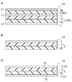
- FIG. 1A to 1C are schematic sectional views showing a multilayer printed wiring board according to an embodiment of the present invention.
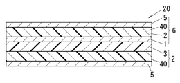
- FIG. 2 is a schematic cross-sectional view showing a multilayer metal-clad laminate according to an embodiment of the present invention.
- 3A to 3E are schematic cross-sectional views showing a plurality of examples of the insulating layer of the above multilayer printed wiring board or multilayer metal-clad laminate.
- 4A is a schematic cross-sectional view showing an example of a metal-clad laminate that can be a material of the multilayer printed wiring board or the multilayer metal-clad laminate
- FIG. 4B is a material of the multilayer printed wiring board or the multilayer metal-clad laminate. It is a schematic sectional drawing which shows an example of the printed wiring board which can become.
- the multilayer metal-clad laminate 20 of this embodiment will be described.
- the multilayer metal-clad laminate 20 can be used as a material for a multilayer printed wiring board 10 described later.
- FIG. 2 shows an example of the multilayer metal-clad laminate 20.
- the multilayer metal-clad laminate 20 has one or more conductor layers 1 and one or more insulating layers 2.
- the multilayer metal-clad laminate 20 shown in FIG. 2 has one conductor layer 1 and two insulating layers 2, but the number of each of the conductor layer 1 and the insulating layer 2 is at least one or more. If it is, it will not specifically limit.
- the multilayer metal-clad laminate 20 may have one conductor layer 1 and one insulating layer 2, or two conductor layers 1 and one insulating layer 2. You may have.
- the conductor layer 1 is actually formed by providing predetermined conductor patterns constituting various circuits, but FIG. 2 shows the conductor layer 1 in a simplified manner.
- the insulating layer 2 is a layer having electrical insulation. As will be described later, the insulating layer 2 may be formed of one type of resin layer, or two or more types of resin layers may be formed adjacent to each other. Thus, the insulating layer 2 may be expressed as the insulating portion 2 because two or more types of resin layers may be formed adjacent to each other.
- the multilayer metal-clad laminate 20 is formed by alternately laminating one or a plurality of conductor layers 1 and one or a plurality of insulating layers 2 and providing a metal layer 5 on one or both outermost layers.
- the outermost layer is the outermost layer. In this case, the outermost layer is the insulating layer 2.
- this one insulating layer 2 is the outermost layer. Therefore, one conductor layer 1 is provided on one surface of the one insulating layer 2, and one metal layer 5 is provided on the other surface.
- FIG. 2 when the multilayer metal-clad laminate 20 has one conductor layer and two insulating layers 2, each of the two insulating layers 2 is the outermost layer.
- the multilayer metal-clad laminate 20 shown in FIG. 2 has one metal layer 5 on each of the two insulating layers 2 and has a total of two metal layers 5, but only one metal layer 5. It may be.
- the metal layer 5 is, for example, a layer made of metal spreading over one surface.
- the multilayer metal-clad laminate 20 shown in FIG. 2 has at least one conductor layer 1 inside, and has a metal layer 5 on one side or both sides.
- the insulating layer 2 is laminated so as to sandwich the conductor layer 1, and the metal layer 5 is arranged on both outermost insulating layers 2 in the thickness direction (lamination direction). ing.
- the multilayer metal-clad laminate 20 can be manufactured using, for example, a printed wiring board 6 described later, a resin base material, and a metal foil such as a copper foil.
- the insulating layer 2 is formed by the resin base material.
- a metal layer 5 is formed by the metal foil. By removing unnecessary portions of the metal layer 5, the conductor layer 1 is formed.
- the resin base material examples include polyolefin resin sheets and non-polyolefin resin sheets.
- the non-polyolefin resin sheet include a fluororesin film, a polyphenylene ether (PPE) resin film, a polyamideimide (PAI) resin film, and a polyimide (PI) resin film. Note that there is no substantial difference between the sheet and the film in concept.
- the polyolefin resin sheet is formed into a sheet shape with a polyolefin resin.
- the polyolefin resin sheet 3 can be formed on the polyolefin resin sheet.
- the polyolefin resin sheet is used as an adhesive sheet.
- the adhesive sheet is a sheet having adhesiveness.
- the polyolefin resin sheet may have a glass cloth inside and be reinforced with the glass cloth.
- the non-polyolefin resin sheet is formed of a non-polyolefin resin into a sheet shape.
- Non-polyolefin resin is resin except polyolefin resin.
- Specific examples of the non-polyolefin resin include a fluororesin, a polyphenylene ether resin, a polyamideimide resin, and a polyimide resin.
- the non-polyolefin resin sheet can form the non-polyolefin resin layer 40.
- the non-polyolefin resin layer 40 is a resin layer excluding the polyolefin resin layer 3.
- the non-polyolefin resin layer 40 is one or more resin layers selected from the group consisting of a fluororesin layer, a polyphenylene ether resin layer, a polyamideimide resin layer, and a polyimide resin layer.
- the non-polyolefin resin sheet may have a glass cloth inside and be reinforced with the glass cloth.
- the fluororesin film is formed of a fluororesin into a film shape.
- the fluororesin film can form a fluororesin layer.
- the fluororesin film has a glass cloth inside and is reinforced with the glass cloth.
- the fluororesin film reinforced with glass cloth can achieve both reduction in dielectric constant and reduction in dielectric loss tangent and improvement in dimensional stability.
- the fluororesin is a synthetic resin obtained by polymerizing an olefin containing fluorine. Specific examples of the fluororesin include polytetrafluoroethylene.
- the polyphenylene ether resin film is formed into a film with polyphenylene ether resin.
- the polyphenylene ether resin film can form a polyphenylene ether resin layer.
- the polyphenylene ether resin film has a glass cloth inside and is reinforced with the glass cloth.
- the polyphenylene ether resin film reinforced with glass cloth can achieve both reduction in dielectric constant and reduction in dielectric loss tangent and improvement in dimensional stability.
- the polyphenylene ether resin is a polymer of 2,6-dimethylphenylene oxide.
- the polyphenylene ether resin includes a modified polyphenylene ether resin.
- the modified polyphenylene ether resin is a polymer alloy of a polyphenylene ether resin and another resin such as a polystyrene resin.
- the polyamide-imide resin film is formed into a film with a polyamide-imide resin.
- the polyamide-imide resin film can form a polyamide-imide resin layer.
- the polyamideimide resin film has a glass cloth inside and may be reinforced with the glass cloth.
- the polyimide resin film is formed of a polyimide resin into a film shape.
- the polyimide resin film can form a polyimide resin layer.
- the polyimide resin film has a glass cloth inside and may be reinforced with the glass cloth.
- each insulating layer 2 of the one or more insulating layers 2 is composed of a polyolefin resin layer 3, a fluororesin layer, a polyphenylene ether resin layer, a polyamideimide resin layer, and a polyimide resin layer. It consists of one or more layers. That is, each insulating layer 2 may have only one layer, or may have two or more adjacent layers.
- One insulating layer 2 is composed of one or more of a polyolefin resin layer 3 and a non-polyolefin resin layer 40 (four types). That is, one insulating layer 2 is composed of one or more of five types of resin layers (polyolefin resin layer 3, fluororesin layer, polyphenylene ether resin layer, polyamideimide resin layer, polyimide resin layer).
- one insulating layer 2 is formed with one kind of resin layer
- one insulating layer 2 is composed of one layer.
- one insulating layer 2 is not necessarily composed of two layers, and may be composed of three or more layers (for example, FIG. 3C described later). And FIG. 3D).
- one insulating layer 2 when one insulating layer 2 is formed with three types of resin layers, one insulating layer 2 is not necessarily composed of three layers, and may be composed of four or more layers. Similarly, when one insulating layer 2 is formed of four types of resin layers, one insulating layer 2 is not necessarily composed of four layers, and may be composed of five or more layers. Similarly, when one insulating layer 2 is formed of five types of resin layers, one insulating layer 2 is not necessarily composed of five layers, and may be composed of six or more layers. That is, when one insulating layer 2 is formed of two or more types of resin layers, the number of types of resin layers may or may not match. When one insulating layer 2 is formed of two or more types of resin layers, the arrangement in the thickness direction (stacking direction) is not particularly limited.
- At least one insulating layer 2 among the one or more insulating layers 2 includes a polyolefin resin layer 3. That is, when the multilayer metal-clad laminate 20 has only one insulating layer 2, the one insulating layer 2 includes the polyolefin resin layer 3. When the multilayer metal-clad laminate 20 has a plurality of insulating layers 2, it is sufficient that at least one insulating layer 2 includes the polyolefin resin layer 3. Of course, all the insulating layers 2 may include the polyolefin resin layer 3. Good.
- the polyolefin resin layer 3 has good adhesion to the non-polyolefin resin layer 40. That is, the polyolefin resin layer 3 has good adhesion to each of the fluororesin layer, polyphenylene ether resin layer, polyamideimide resin layer, and polyimide resin layer.
- FIG. 3A to 3E show specific examples of specific layer structures of one insulating layer 2.
- FIG. 3A to 3E show specific examples of specific layer structures of one insulating layer 2.
- the insulating layer 2 shown in FIG. 3A consists of one kind of resin layer. Specifically, FIG. 3A shows the insulating layer 2 formed of only the polyolefin resin layer 3.
- This insulating layer 2 can be formed by heat-curing a polyolefin resin sheet. In this case, only one polyolefin resin sheet can be used, or two or more can be stacked and used.
- the polyolefin resin layer 3 formed by stacking two or more polyolefin resin sheets is a single layer.
- the insulating layer 2 shown in FIG. 3B is also made of one type of resin layer. Specifically, FIG. 3B shows the insulating layer 2 formed of only the non-polyolefin resin layer 40. More specifically, FIG. 3B shows the insulating layer 2 formed of only one of a fluororesin layer, a polyphenylene ether resin layer, a polyamideimide resin layer, and a polyimide resin layer.
- This insulating layer 2 is made of a fluororesin film, a fluororesin film reinforced with glass cloth, a polyphenylene ether resin film, a polyphenylene ether resin film reinforced with glass cloth, a polyamideimide resin film, and a polyimide resin film as a resin base material.
- the resin film can form only with the resin film in any one of them.
- only one resin base material can be used, or two or more resin base materials can be used in an overlapping manner.
- the resin layer formed by overlapping two or more of the same resin base materials is one layer.
- the insulating layer 2 shown in FIG. 3C comprises two types of resin layers, and has a three-layer structure in which one type of resin layer is sandwiched between other types of resin layers.
- FIG. 3C shows the insulating layer 2 formed by laminating the non-polyolefin resin layer 40 on both sides of the polyolefin resin layer 3.
- FIG. 3C shows an insulating layer 2 formed by laminating one of a fluororesin layer, a polyphenylene ether resin layer, a polyamideimide resin layer, and a polyimide resin layer on both sides of the polyolefin resin layer 3. Indicates.
- This insulating layer 2 is one of a fluororesin film, a fluororesin film reinforced with glass cloth, a polyphenylene ether resin film, a polyphenylene ether resin film reinforced with glass cloth, a polyamideimide resin film, and a polyimide resin film.
- a resin sheet can be laminated on both sides of a polyolefin resin sheet to form a composite sheet, which can be formed by heat curing.
- the insulating layer 2 shown in FIG. 3D is also composed of two types of resin layers, and has a three-layer structure in which a certain type of resin layer is sandwiched between different types of resin layers.
- FIG. 3D shows the insulating layer 2 formed by laminating the polyolefin resin layer 3 on both sides of the non-polyolefin resin layer 40.
- FIG. 3D shows an insulating layer 2 formed by laminating a polyolefin resin layer 3 on both sides of any one of a fluororesin layer, a polyphenylene ether resin layer, a polyamideimide resin layer, and a polyimide resin layer. Indicates.
- This insulating layer 2 is one of a fluororesin film, a fluororesin film reinforced with glass cloth, a polyphenylene ether resin film, a polyphenylene ether resin film reinforced with glass cloth, a polyamideimide resin film, and a polyimide resin film. It can be formed by laminating a polyolefin resin sheet on both sides of the resin film to form a composite sheet and then heat-curing it.
- the insulating layer 2 shown in FIG. 3E is also composed of two types of resin layers, and has a two-layer structure in which these resin layers are stacked.
- FIG. 3E shows an insulating layer 2 formed by laminating a non-polyolefin resin layer 40 and a polyolefin resin layer 3.
- FIG. 3E shows an insulating layer 2 formed by laminating one of a fluororesin layer, a polyphenylene ether resin layer, a polyamideimide resin layer, and a polyimide resin layer and a polyolefin resin layer 3. Indicates.
- This insulating layer 2 is one of a fluororesin film, a fluororesin film reinforced with glass cloth, a polyphenylene ether resin film, a polyphenylene ether resin film reinforced with glass cloth, a polyamideimide resin film, and a polyimide resin film.
- a composite film can be formed by laminating a resin film and a polyolefin resin sheet, and this can be formed by heat curing.
- polyolefin resin sheet, fluororesin film, fluororesin film reinforced with glass cloth, polyphenylene ether resin film, polyphenylene ether resin film reinforced with glass cloth, polyamideimide resin film, polyimide resin film Can be used only one each, or two or more can be used in an overlapping manner.
- the resin layer formed by overlapping two or more of the same resin base materials is one layer.
- the polyolefin resin layer 3 contains the component (A) polyolefin elastomer and the component (B) thermosetting resin, and the proportion of the component (A) polyolefin elastomer in the entire polyolefin resin layer 3 is 50 to 95% by mass. Preferably there is.
- the polyolefin resin layer 3 contains many component (A) polyolefin-type elastomers, the heat resistance of the multilayer metal-clad laminate 20 and the multilayer printed wiring board 10 manufactured by using this is improved. In particular, it is effective for improving solder heat resistance after moisture absorption. Furthermore, the flexibility of the multilayer metal-clad laminate 20 and the multilayer printed wiring board 10 is increased, and the flexibility is further improved.
- Polyolefin elastomer is polystyrene-poly (ethylene / propylene) block-polystyrene copolymer, polystyrene-poly (ethylene-ethylene / propylene) block-polystyrene copolymer, polystyrene-poly (ethylene / butylene) block.
- polystyrene-polyisoprene block copolymer polystyrene-polyisoprene block copolymer, hydrogenated polystyrene-polyisoprene-polybutadiene block copolymer, polystyrene-poly (butadiene / butylene) block-polystyrene copolymer, ethylene-glycidyl methacrylate copolymer
- thermosetting resin is preferably one or more selected from the group consisting of epoxy resins, phenol resins, bismaleimide resins, and polyphenylene ether oligomers having vinyl groups at both ends.
- epoxy resin include a dicyclopentadiene type epoxy resin.
- the polyolefin resin layer 3 can further contain a component (C) curing accelerator.
- C component (C) curing accelerator.
- the curing accelerator include 2-ethyl-4-methylimidazole.
- the polyolefin resin layer 3 can further contain a component (D) filler.
- a component (D) filler is silica.
- the multilayer metal-clad laminate 20 can be manufactured as follows, for example.
- the metal-clad laminate 60 has fewer layers than the multilayer metal-clad laminate 20 and is a material for the multilayer metal-clad laminate 20.
- the metal-clad laminate 60 include a single-sided metal-clad laminate or a double-sided metal-clad laminate in which a metal foil is attached to one or both sides of the insulating layer 2 shown in FIGS. 3A to 3E.
- FIG. 4A shows a metal-clad laminate 60 (double-sided metal-clad laminate) formed by providing metal layers 5 on both sides of the insulating layer 2 shown in FIG. 3B.
- the insulating layer 2 is made of one type of resin layer.
- the insulating layer 2 is formed of a non-polyolefin resin layer 40 (a resin layer of any one of a fluororesin layer, a polyphenylene ether resin layer, a polyamideimide resin layer, and a polyimide resin layer), and the metal layer 5 is a metal It is made of foil.
- a non-polyolefin resin layer 40 a resin layer of any one of a fluororesin layer, a polyphenylene ether resin layer, a polyamideimide resin layer, and a polyimide resin layer
- the metal layer 5 is a metal It is made of foil.
- a metal-clad laminate 60 in which a metal foil is bonded to both surfaces of a non-polyolefin resin layer 40 (a resin layer of a fluororesin layer, a polyphenylene ether resin layer, a polyamideimide resin layer, or a polyimide resin layer) (see FIG. 4A)
- a non-polyolefin resin layer 40 a resin layer of a fluororesin layer, a polyphenylene ether resin layer, a polyamideimide resin layer, or a polyimide resin layer
- the unnecessary portion of the metal layer 5 on one side of the metal-clad laminate 60 shown in FIG. 4A is removed to form the conductor layer 1, and the metal-clad laminate 60 is processed into a printed wiring board 6 as shown in FIG. 4B. More specifically, in FIG. 4B, an unnecessary portion of one outermost metal layer 5 of the metal-clad laminate 60 is removed by etching or the like to form the conductor layer 1, and the other outermost metal layer 5 is left as it is. ing.
- the conductor layer 1 is formed by providing predetermined conductor patterns constituting various circuits. In FIG. 4B, the conductor layer 1 is shown in a simplified manner.
- the conductor layer 1 When forming the conductor layer 1 including a circuit that requires high-speed signal transmission or a circuit that has a long transmission distance, the conductor layer 1 includes a non-polyolefin resin layer 40 (a fluororesin layer, It is preferably formed in contact with a resin layer of any one of a polyphenylene ether resin layer, a polyamideimide resin layer, and a polyimide resin layer. Thereby, the transmission loss of the high-speed signal of the multilayer printed wiring board 10 can be reduced.
- a non-polyolefin resin layer 40 a fluororesin layer, It is preferably formed in contact with a resin layer of any one of a polyphenylene ether resin layer, a polyamideimide resin layer, and a polyimide resin layer.
- a multilayer metal-clad laminate 20 as shown in FIG. 2 can be obtained by laminating a resin film and a resin film of any one of a polyimide resin film) and heating and pressing it.
- the multilayer metal-clad laminate 20 shown in FIG. 2 includes a polyolefin resin sheet for forming the polyolefin resin layer 3 and a non-polyolefin resin layer 40 on the conductor layer 1 of the printed wiring board 6 shown in FIG. 4B.
- Non-polyolefin resin sheet for forming fluorine resin film for forming fluororesin layer, polyphenylene ether resin film for forming polyphenylene ether resin layer, polyamideimide resin film and polyimide for forming polyamideimide resin layer
- Any one of the polyimide resin films for forming the resin layer) and the metal foil for forming the metal layer 5 are stacked in this order, and can be manufactured by heating and pressing.
- Two insulating layers 2 adjacent to the polyolefin resin layer 3 and the non-polyolefin resin layer 40 (a resin layer selected from a fluororesin layer, a polyphenylene ether resin layer, a polyamideimide resin layer, and a polyimide resin layer). Is formed.
- a printed wiring board 6 a polyolefin resin sheet, a non-polyolefin resin sheet (fluorine resin film, polyphenylene ether resin film, polyamideimide resin film, polyimide resin film), metal foil
- a polyolefin resin sheet fluorine resin film, polyphenylene ether resin film, polyamideimide resin film, polyimide resin film
- metal foil By increasing the number of sheets, it is possible to increase the number of layers of the multilayer metal-clad laminate 20 and realize further multilayering.
- the 2 has a layer structure in which the printed wiring board 6 is disposed outside.
- the conductor layer 1 is provided on one outermost layer of the printed wiring board 6 to be used, and the metal layer 5 is provided on the other outermost layer (see FIG. 4B).
- the conductor layer 1 includes predetermined conductor patterns constituting various circuits.
- the metal layer 5 is a layer made of, for example, a metal spreading over one surface. Then, at the time of manufacturing the multilayer metal-clad laminate 20, the printed wiring board 6 is arranged so that the conductor layer 1 is on the inner side and the metal layer 5 is on the outer side.
- the multilayer metal-clad laminate 20 may have a layer configuration in which the entire printed wiring board 6 is disposed inside.
- the conductor layer 1 is provided on both outermost layers of the printed wiring board 6 to be used. All of these conductor layers 1 are included in the multilayer metal-clad laminate 20.
- each insulating layer 2 of the one or more insulating layers 2 is composed of a polyolefin resin layer 3, a fluororesin layer, a polyphenylene ether resin layer, a polyamideimide resin layer, and a polyimide resin layer. It consists of one or a plurality of layers, and at least one of the one or more insulating layers 2 includes a polyolefin resin layer 3.
- the polyolefin resin layer 3, the fluororesin layer, the polyphenylene ether resin layer, the polyamideimide resin layer, and the polyimide resin layer are all excellent in high frequency characteristics, and the polyolefin resin layer 3 is composed of the other four types of resins. Adhesion with the layer (non-polyolefin resin layer 40) is good. Thereby, the transmission loss of the high-speed signal of the multilayer printed wiring board 10 obtained by processing the multilayer metal-clad laminate 20 can be reduced.
- the multilayer metal-clad laminate 20 shown in FIG. 2 has two insulating layers 2.
- the first insulating layer 2 is made of one type of resin layer. Specifically, the first insulating layer 2 is composed of only the non-polyolefin resin layer 40. More specifically, the first insulating layer 2 is composed of one of a fluororesin layer, a polyphenylene ether resin layer, a polyamideimide resin layer, and a polyimide resin layer.
- the second insulating layer 2 consists of two types of resin layers. Specifically, the second insulating layer 2 includes two layers including a polyolefin resin layer 3 and a non-polyolefin resin layer 40. More specifically, the second insulating layer 2 includes a polyolefin resin layer 3 and further includes two layers including one of a fluororesin layer, a polyphenylene ether resin layer, a polyamideimide resin layer, and a polyimide resin layer. Consists of.
- the conductor layer 1 including a circuit that requires transmission of a high-speed signal or a circuit with a long transmission distance is composed of a non-polyolefin resin layer 40 (a fluororesin layer, a polyphenylene ether resin layer, a polyamideimide resin layer, a polyimide resin layer). It is preferable to contact any one of the resin layers. Thereby, the transmission loss of the high-speed signal of the multilayer printed wiring board 10 obtained by processing the multilayer metal-clad laminate 20 can be reduced.
- the multi-layering can be performed only once or divided into two or more times. Further, the number of layers is not particularly limited and is not limited according to the design of the target multilayer metal-clad laminate 20.
- the multilayer printed wiring board 10 of this embodiment is demonstrated.
- the multilayer printed wiring board 10 can be manufactured, for example, by forming the conductor layer 1 by removing unnecessary portions of one or both of the outermost metal layers 5 of the multilayer metal-clad laminate 20 by etching or the like.
- FIG. 1A shows an example of the multilayer printed wiring board 10 of the present embodiment.
- the multilayer printed wiring board 10 has one or more conductor layers 1 and one or more insulating layers 2.
- the multilayer printed wiring board 10 shown in FIG. 1A has three conductor layers 1 and two insulating layers 2. However, the number of each of the conductor layers 1 and the insulating layers 2 is at least one or more. If there is no particular limitation.
- the multilayer printed wiring board 10 is formed by alternately laminating one or more conductor layers 1 and one or more insulating layers 2.
- the conductor layer 1 includes, for example, a signal layer, a power supply layer, and a ground layer.
- the conductor layer 1 is formed by providing predetermined conductor patterns constituting various circuits.
- the conductor layer 1 is illustrated in a simplified manner. .
- via holes for example, through-hole plating for electrically connecting different conductor layers 1 are not shown.
- each insulating layer 2 of the one or more insulating layers 2 is one of a polyolefin resin layer 3, a fluororesin layer, a polyphenylene ether resin layer, a polyamideimide resin layer, and a polyimide resin layer. It consists of one or a plurality of layers, and at least one insulating layer 2 of the one or more insulating layers 2 includes a polyolefin resin layer 3.
- the multilayer printed wiring board 10 shown in FIG. 1A has two insulating layers 2.
- the first insulating layer 2 is made of one type of resin layer. Specifically, the first insulating layer 2 is composed of only the non-polyolefin resin layer 40. More specifically, the first insulating layer 2 is composed of one of a fluororesin layer, a polyphenylene ether resin layer, a polyamideimide resin layer, and a polyimide resin layer.
- the second insulating layer 2 consists of two types of resin layers. Specifically, the second insulating layer 2 includes two layers including a polyolefin resin layer 3 and a non-polyolefin resin layer 40. More specifically, the second insulating layer 2 includes a polyolefin resin layer 3 and further includes two layers including one of a fluororesin layer, a polyphenylene ether resin layer, a polyamideimide resin layer, and a polyimide resin layer. Consists of.
- the polyolefin resin layer 3, the fluororesin layer, the polyphenylene ether resin layer, the polyamideimide resin layer, and the polyimide resin layer are all excellent in high frequency characteristics, and the polyolefin resin layer 3 is composed of the other four types of resins. Adhesion with the layer (non-polyolefin resin layer 40) is good. Thereby, the multilayer printed wiring board 10 has excellent high frequency characteristics. That is, the transmission loss of the high-speed signal of the multilayer printed wiring board 10 can be reduced.
- the polyolefin resin layer 3 preferably has a storage elastic modulus of 10 5 to 10 8 Pa at 25 ° C. to 150 ° C. after being treated at 180 ° C. for 60 minutes. Thereby, the thermal shock resistance of the multilayer printed wiring board 10 can be improved, disconnection such as via-hole plating or through-hole plating can be suppressed, and the effect of improving solder heat resistance during reflow can be achieved.
- the multilayer printed wiring board 10 has two insulating layers 2, one insulating layer 2 (first insulating layer 201) of the two insulating layers 2 is provided.
- the non-polyolefin resin layer 40 is included, and the remaining one insulating layer 2 (second insulating layer 202) of the two insulating layers 2 includes the polyolefin resin layer 3.
- the first insulating layer 201 includes one or more of a fluororesin layer, a polyphenylene ether resin layer, a polyamideimide resin layer, and a polyimide resin layer
- the second insulating layer 202 is a polyolefin resin layer. 3 is included.
- the first insulating layer 201 may further include the polyolefin resin layer 3
- the second insulating layer 202 may further include the non-polyolefin resin layer 40.
- the first insulating layer 201 includes one or more of a fluororesin layer, a polyphenylene ether resin layer, a polyamideimide resin layer, and a polyimide resin layer, and the second insulating layer 202.
- the transmission loss of a high-speed signal can be reduced by including the polyolefin resin layer 3.
- FIG. 1B shows another example of the multilayer printed wiring board 10 of the present embodiment.
- the multilayer printed wiring board 10 has one insulating layer 2 as one or a plurality of insulating layers 2. Furthermore, this multilayer printed wiring board 10 has one conductor layer 1 laminated on one side of one insulating layer 2 as one or a plurality of conductor layers 1.
- One insulating layer 2 includes a non-polyolefin resin layer 40 and a polyolefin resin layer 3. That is, one insulating layer 2 includes one or more of a fluororesin layer, a polyphenylene ether resin layer, a polyamideimide resin layer, and a polyimide resin layer, and includes a polyolefin resin layer 3.
- one insulating layer 2 includes one or more of a fluororesin layer, a polyphenylene ether resin layer, a polyamideimide resin layer, and a polyimide resin layer, and includes a polyolefin resin layer 3.
- a fluororesin layer As described above, one insulating layer 2 includes one or more of a fluororesin layer, a polyphenylene ether resin layer, a polyamideimide resin layer, and a polyimide resin layer, and includes a polyolefin resin layer 3.
- FIG. 1C shows still another example of the multilayer printed wiring board 10 of the present embodiment.
- the multilayer printed wiring board 10 has one insulating layer 2 as one or a plurality of insulating layers 2. Further, the multilayer printed wiring board 10 includes, as one or a plurality of conductor layers 1, a first conductor layer 11 laminated on a first surface 21 of both surfaces of one insulating layer 2, and one insulating layer 2. The second conductor layer 12 is laminated on the second surface 22 of the two surfaces.
- One insulating layer 2 includes a non-polyolefin resin layer 40 and a polyolefin resin layer 3. That is, one insulating layer 2 includes one or more of a fluororesin layer, a polyphenylene ether resin layer, a polyamideimide resin layer, and a polyimide resin layer, and includes a polyolefin resin layer 3.
- one insulating layer 2 includes one or more of a fluororesin layer, a polyphenylene ether resin layer, a polyamideimide resin layer, and a polyimide resin layer, and includes a polyolefin resin layer 3.
- a fluororesin layer As described above, one insulating layer 2 includes one or more of a fluororesin layer, a polyphenylene ether resin layer, a polyamideimide resin layer, and a polyimide resin layer, and includes a polyolefin resin layer 3.
- the multilayer printed wiring board (10) includes one or more conductor layers (1) and one or more insulating layers (2). ).
- the multilayer printed wiring board (10) is formed by alternately laminating the one or more conductor layers (1) and the one or more insulating layers (2).
- Each insulating layer (2) of the one or more insulating layers (2) is a polyolefin resin layer (3), a fluororesin layer, a polyphenylene ether resin layer, a polyamideimide resin layer, or a polyimide resin layer. It consists of one or more layers.
- the at least one insulating layer (2) of the one or more insulating layers (2) includes a polyolefin resin layer (3).
- each insulating layer (2) of the one or more insulating layers (2) is a polyolefin resin layer (3), a fluororesin layer, a polyphenylene ether resin layer, a polyamideimide resin layer, It consists of one or a plurality of polyimide resin layers, and at least one insulating layer (2) of the one or more insulating layers (2) includes a polyolefin resin layer (3). Signal transmission loss can be reduced.
- the one or more insulating layers (2) have one insulating layer (2), As one or a plurality of conductor layers (1), one conductor layer (1) laminated on one side of the one insulating layer (2) is provided.
- the one insulating layer (2) includes one or more of a fluororesin layer, a polyphenylene ether resin layer, a polyamideimide resin layer, and a polyimide resin layer, and includes a polyolefin resin layer (3).
- one insulating layer (2) includes one or more of a fluororesin layer, a polyphenylene ether resin layer, a polyamideimide resin layer, a polyimide resin layer, and a polyolefin resin.
- the one or more insulating layers (2) have one insulating layer (2), As the one or more conductor layers (1), the first conductor layer (11) laminated on the first surface (21) of both surfaces of the one insulating layer (2), and the one insulating layer And a second conductor layer (12) laminated on the second surface (22) of both surfaces of the layer (2).
- the one insulating layer (2) includes one or more of a fluororesin layer, a polyphenylene ether resin layer, a polyamideimide resin layer, and a polyimide resin layer, and includes a polyolefin resin layer (3).
- one insulating layer (2) includes one or more of a fluororesin layer, a polyphenylene ether resin layer, a polyamideimide resin layer, a polyimide resin layer, and a polyolefin resin.
- the one or the plurality of insulating layers (2) has two insulating layers (2), The one or more conductor layers (1) alternately stacked with the two insulating layers (2).
- One insulating layer (2) of the two insulating layers (2) includes one or more of a fluororesin layer, a polyphenylene ether resin layer, a polyamideimide resin layer, and a polyimide resin layer.
- the remaining one insulating layer (2) of the two insulating layers (2) includes a polyolefin resin layer (3).
- one of the two insulating layers (2) is one of a fluororesin layer, a polyphenylene ether resin layer, a polyamideimide resin layer, a polyimide resin layer, or By including a plurality of layers and the remaining one insulating layer (2) of the two insulating layers (2) includes the polyolefin resin layer (3), transmission loss of high-speed signals can be reduced.
- the polyolefin resin layer (3) comprises a component (A) a polyolefin-based elastomer and a component (B) heat.
- a curable resin a component (A) a polyolefin-based elastomer and a component (B) heat.
- the proportion of the component (A) polyolefin elastomer in the entire polyolefin resin layer (3) is 50 to 95% by mass.
- the polyolefin resin layer (3) contains a large amount of the component (A) polyolefin-based elastomer
- the multilayer metal-clad laminate (20) and the multilayer printed wiring board (10) manufactured using the multilayer metal-clad laminate (20) The heat resistance of is improved. In particular, it is effective for improving solder heat resistance after moisture absorption. Furthermore, the flexibility of the multilayer metal-clad laminate (20) and the multilayer printed wiring board (10) is increased, and the flexibility is further improved.
- the component (A) polyolefin elastomer is a polystyrene-poly (ethylene / propylene) block-polystyrene copolymer, polystyrene.
- thermosetting resin is an epoxy resin, a phenol resin, a bismaleimide resin, and both ends. It is one or more selected from the group consisting of vinyl group polyphenylene ether oligomers.
- the polyolefin resin layer (3) further contains a component (C) curing accelerator.
- the polyolefin resin layer (3) further includes a component (D) filler.
- the polyolefin resin layer (3) has a storage elasticity after being treated at 180 ° C. for 60 minutes.
- the rate is 10 5 to 10 8 Pa at 25 ° C. to 150 ° C.
- the multilayer metal-clad laminate (20) of one aspect according to the present invention has one or a plurality of conductor layers (1) and one or a plurality of insulating layers (2).
- the multilayer metal-clad laminate (20) is formed by alternately laminating the one or more conductor layers (1) and the one or more insulating layers (2), and one or both outermost layers have metal layers ( 5) is provided.
- Each insulating layer (2) of the one or more insulating layers (2) is a polyolefin resin layer (3), a fluororesin layer, a polyphenylene ether resin layer, a polyamideimide resin layer, or a polyimide resin layer. It consists of one or more layers.
- the at least one insulating layer (2) of the one or more insulating layers (2) includes a polyolefin resin layer (3).
- each insulating layer (2) of one or a plurality of insulating layers (2) includes a polyolefin resin layer (3), a fluororesin layer, and a polyphenylene ether resin. It consists of one or a plurality of layers, a polyamideimide resin layer, a polyimide resin layer, and at least one insulating layer (2) of the one or more insulating layers (2) is a polyolefin resin layer (3 ), The transmission loss of high-speed signals can be reduced.
- Examples 1 to 5 and Comparative Example 1 a three-layer printed wiring board as shown in FIG. 1A was manufactured.
- the three conductor layers 1 are distinguished from each other by naming them L1 to L3 in order from one outermost layer.
- PCB configuration means the layer configuration of a three-layer printed wiring board.
- L1 / L2 copper-clad laminate (or printed wiring board) means a copper-clad laminate (or printed wiring board) including the conductor layers 1 of L1 and L2.
- expressions such as “three-layer printed wiring board of L1 to L3” mean a three-layer printed wiring board including all the conductor layers 1 of L1 to L3.
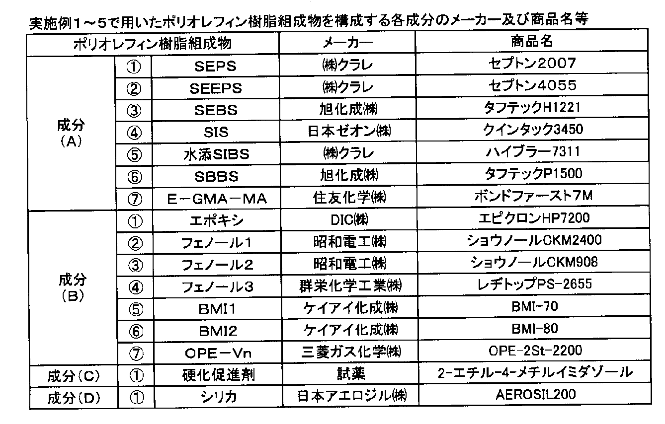
- Table 7 shows a composition table of polyolefin resin compositions for forming the polyolefin resin sheets used in Examples 1 to 5.
- Table 8 shows manufacturers and trade names of the components constituting the polyolefin resin composition.
- Example 1 is composed of eleven types of examples from Example 1- (1) to Example 1- (11). These examples are the same except for the polyolefin resin sheet described later.
- a single-sided copper-clad laminate in which the copper foil on one side of the L1 / L2 high-frequency substrate (double-sided copper-clad laminate) was removed by etching was prepared as an L3 high-frequency substrate.
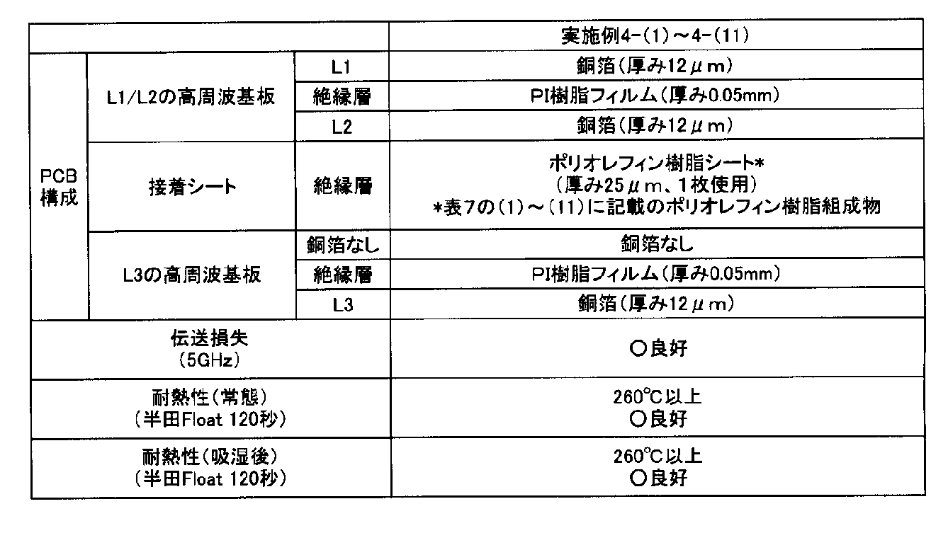
- a polyolefin resin sheet having a thickness of 25 ⁇ m is formed from each type of resin composition of (1) to (11) shown in Table 7, and this polyolefin resin sheet (one sheet) is connected to a printed wiring board of L1 to L2.
- a three-layer metal-clad laminate was produced by interposing between the L3 single-sided copper-clad laminate and heat-pressing it at 180 ° C. for 60 minutes.
- a three-layer printed wiring board was manufactured by forming a ground layer on L1 and L3 of the three-layer metal-clad laminate.
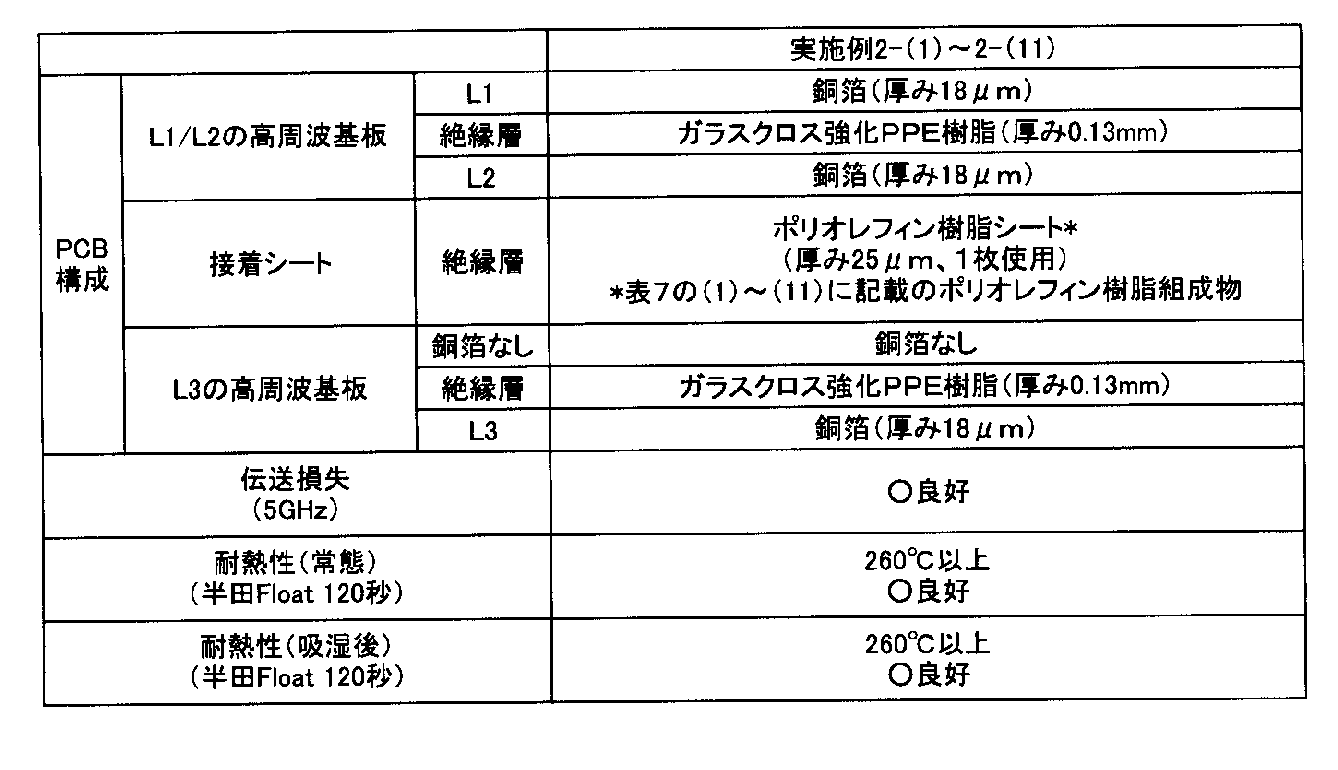
- Example 2 The second embodiment is composed of eleven types of embodiments from the embodiment 2- (1) to the embodiment 2- (11). These examples are the same except for the polyolefin resin sheet described later.
- a copper-clad laminate “R-5775K MEGRON6” (copper foil thickness 18 ⁇ m, glass cloth reinforced PPE resin thickness 0.13 mm) manufactured by Panasonic Corporation was prepared as an L1 / L2 high-frequency substrate.
- a single-sided copper-clad laminate in which the copper foil on one side of the L1 / L2 high-frequency substrate (double-sided copper-clad laminate) was removed by etching was prepared as an L3 high-frequency substrate.
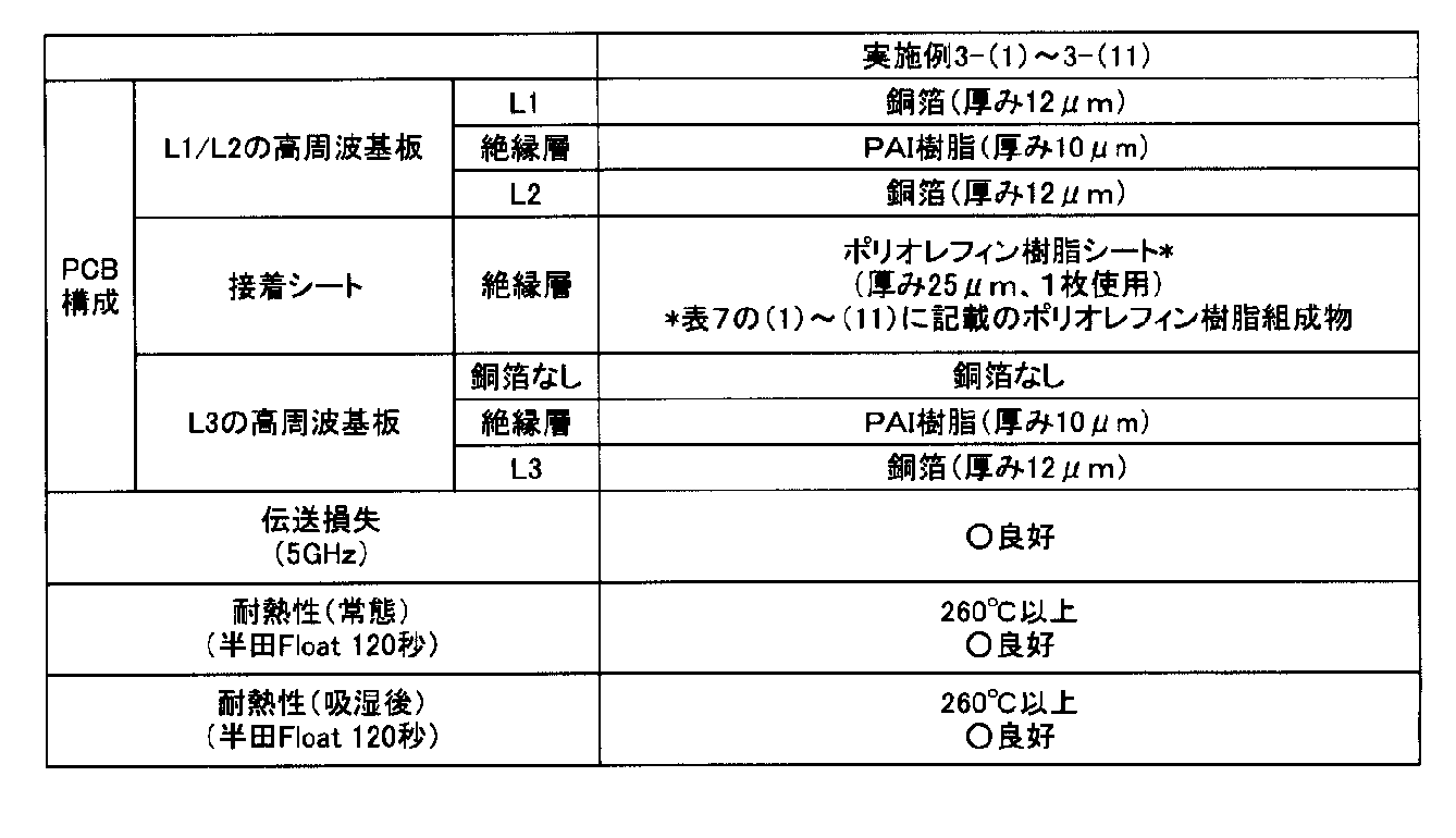
- Example 3 The third embodiment is composed of eleven types of embodiments from the embodiment 3- (1) to the embodiment 3- (11). These examples are the same except for the polyolefin resin sheet described later.
- a L1 / L2 high frequency substrate was manufactured and prepared as follows. First, a PAI resin described later was applied on a copper foil having a thickness of 12 ⁇ m so as to have a thickness of 5 ⁇ m and dried to prepare a substrate. Another sheet of the same substrate was produced. Next, the PAI resins of these substrates were overlapped and heated and pressed to bond the two substrates to produce a double-sided copper-clad laminate (copper foil thickness 12 ⁇ m, PAI resin thickness 10 ⁇ m). This double-sided copper-clad laminate was prepared as an L1 / L2 high-frequency substrate.
- the above PAI resin was prepared as follows. 192 g of trimellitic anhydride (manufactured by Nacalai Tesque), 211 g of 4,4′-diisocyanato-3,3′-dimethylbiphenyl, 35 g of tolylene 2,4-diisocyanate, 1 g of diazabicycloundecene (manufactured by San Apro) , And 2482 g of N, N-dimethylacetamide (DMAC, manufactured by Nacalai Tesque Co., Ltd.), the polymer concentration was adjusted to 15% by mass, and the resulting mixture was heated to 100 ° C. over 1 hour.
- trimellitic anhydride manufactured by Nacalai Tesque
- DMAC N-dimethylacetamide
- the reaction was allowed to proceed by allowing it to warm, followed by maintaining the mixture at 100 ° C. for 6 hours.
- the polymer concentration was then adjusted to 10 wt% by adding an additional 1460 g of DMAC to the mixture, and the mixture was subsequently cooled to room temperature.
- a resin solution in which polyamideimide was dissolved was obtained. This was used as a PAI resin for the production of the above L1 / L2 high-frequency substrate.
- a single-sided copper-clad laminate in which the copper foil on one side of the L1 / L2 high-frequency substrate (double-sided copper-clad laminate) was removed by etching was prepared as an L3 high-frequency substrate.
- Example 4 The fourth embodiment is composed of eleven types of embodiments of the embodiment 4- (1) to the embodiment 4- (11). These examples are the same except for the polyolefin resin sheet described later.
- a copper-clad laminate “R-F775 23EJ-M” (copper foil thickness 12 ⁇ m, PI resin thickness 0.05 mm) manufactured by Panasonic Corporation was prepared as an L1 / L2 high-frequency substrate.
- a single-sided copper-clad laminate in which the copper foil on one side of the L1 / L2 high-frequency substrate (double-sided copper-clad laminate) was removed by etching was prepared as an L3 high-frequency substrate.
- Example 5 Example 1 except that a polyolefin resin sheet (1 sheet) having a thickness of 25 ⁇ m formed of the resin composition of (12) shown in Table 7 was used as the polyolefin resin sheet instead of the polyolefin resin sheet of Example 1.
- a three-layer printed wiring board was manufactured by the same method as described above.
- Example 1 A three-layer printed wiring board is manufactured in the same manner as in Example 2, except that a glass cloth reinforced polyphenylene ether resin prepreg (prepreg reinforced with glass cloth and containing polyphenylene ether resin) having a thickness of 100 ⁇ m is used as the adhesive sheet. did.
- Examples 1 to 4 were superior in solder heat resistance after moisture absorption compared to Example 5. This result is considered to be because the proportion of the component (A) polyolefin-based elastomer is higher in Examples 1 to 4 than in Example 5.
Landscapes
- Engineering & Computer Science (AREA)
- Microelectronics & Electronic Packaging (AREA)
- Physics & Mathematics (AREA)
- Spectroscopy & Molecular Physics (AREA)
- Manufacturing & Machinery (AREA)
- Laminated Bodies (AREA)
- Production Of Multi-Layered Print Wiring Board (AREA)
Abstract
Description
前記多層プリント配線板は、前記1つ又は複数の導体層及び前記1つ又は複数の絶縁層を交互に積層して形成され、
前記1つ又は複数の絶縁層のうちの各絶縁層が、ポリオレフィン樹脂層、フッ素樹脂層、ポリフェニレンエーテル樹脂層、ポリアミドイミド樹脂層、ポリイミド樹脂層のうちの1つ又は複数の層からなり、
前記1つ又は複数の絶縁層のうちの少なくとも1つの絶縁層が、ポリオレフィン樹脂層を含む。
まず本実施形態の多層金属張積層板20について説明する。多層金属張積層板20は、後述の多層プリント配線板10の材料として用いることができる。
多層金属張積層板20は、例えば、次のようにして製造することができる。
次に本実施形態の多層プリント配線板10について説明する。多層プリント配線板10は、例えば、多層金属張積層板20の一方又は両方の最外層の金属層5の不要部分をエッチングなどにより除去して導体層1を形成することによって製造することができる。
前記1つ又は複数の導体層(1)として、前記1つの絶縁層(2)の片面に積層された1つの導体層(1)を有する。
前記1つ又は複数の導体層(1)として、前記1つの絶縁層(2)の両面のうちの第1面(21)に積層された第1の導体層(11)と、前記1つの絶縁層(2)の両面のうちの第2面(22)に積層された第2の導体層(12)とを有する。
前記2つの絶縁層(2)と交互に積層された前記1つ又は複数の導体層(1)を有する。
実施例1は、実施例1-(1)~実施例1-(11)の11種類の実施例で構成される。これらの実施例は、後述のポリオレフィン樹脂シートのみが異なるだけで、その他は同じである。
実施例2は、実施例2-(1)~実施例2-(11)の11種類の実施例で構成される。これらの実施例は、後述のポリオレフィン樹脂シートのみが異なるだけで、その他は同じである。
実施例3は、実施例3-(1)~実施例3-(11)の11種類の実施例で構成される。これらの実施例は、後述のポリオレフィン樹脂シートのみが異なるだけで、その他は同じである。
実施例4は、実施例4-(1)~実施例4-(11)の11種類の実施例で構成される。これらの実施例は、後述のポリオレフィン樹脂シートのみが異なるだけで、その他は同じである。
ポリオレフィン樹脂シートとして、表7に示す(12)の樹脂組成物で形成された厚み25μmのポリオレフィン樹脂シート(1枚)を、実施例1のポリオレフィン樹脂シートの代わりに用いた以外は、実施例1と同じ方法で3層プリント配線板を製造した。
接着シートとして、厚み100μmのガラスクロス強化ポリフェニレンエーテル樹脂プリプレグ(ガラスクロスで強化され、ポリフェニレンエーテル樹脂を含有するプリプレグ)を用いたこと以外は、実施例2と同じ方法で3層プリント配線板を製造した。
各3層プリント配線板について、L2の信号層の5GHzでの伝送損失を測定した。その結果を表1~表6に示す。
各3層プリント配線板について、L1に25mm角の銅パターンを形成し、常態(30℃以下、60%Rh以下)及び吸湿(60℃、60%Rh、120H)後の半田Floatでの耐熱性(JIS C 5012 10.4.1)を測定した。その結果を表1~表6に示す。



2 絶縁層
3 ポリオレフィン樹脂層
5 金属層
10 多層プリント配線板
11 第1の導体層
12 第2の導体層
20 多層金属張積層板
21 第1面
22 第2面
40 非ポリオレフィン樹脂層
201 第1の絶縁層
202 第2の絶縁層
Claims (11)
- 多層プリント配線板であって、
前記多層プリント配線板は、1つ又は複数の導体層と、1つ又は複数の絶縁層とを有し、
前記多層プリント配線板は、前記1つ又は複数の導体層及び前記1つ又は複数の絶縁層を交互に積層して形成され、
前記1つ又は複数の絶縁層のうちの各絶縁層が、ポリオレフィン樹脂層、フッ素樹脂層、ポリフェニレンエーテル樹脂層、ポリアミドイミド樹脂層、ポリイミド樹脂層のうちの1つ又は複数の層からなり、
前記1つ又は複数の絶縁層のうちの少なくとも1つの絶縁層が、ポリオレフィン樹脂層を含む、
多層プリント配線板。 - 前記多層プリント配線板は、
前記1つ又は複数の絶縁層として、1つの絶縁層を有し、
前記1つ又は複数の導体層として、前記1つの絶縁層の片面に積層された1つの導体層を有し、
前記1つの絶縁層が、フッ素樹脂層、ポリフェニレンエーテル樹脂層、ポリアミドイミド樹脂層、ポリイミド樹脂層のうちの1つ又は複数の層を含み、かつ、ポリオレフィン樹脂層を含む、
請求項1に記載の多層プリント配線板。 - 前記多層プリント配線板は、
前記1つ又は複数の絶縁層として、1つの絶縁層を有し、
前記1つ又は複数の導体層として、前記1つの絶縁層の両面のうちの第1面に積層された第1の導体層と、前記1つの絶縁層の両面のうちの第2面に積層された第2の導体層とを有し、
前記1つの絶縁層が、フッ素樹脂層、ポリフェニレンエーテル樹脂層、ポリアミドイミド樹脂層、ポリイミド樹脂層のうちの1つ又は複数の層を含み、かつ、ポリオレフィン樹脂層を含む、
請求項1に記載の多層プリント配線板。 - 前記多層プリント配線板は、
前記1つ又は複数の絶縁層として、2つの絶縁層を有し、
前記2つの絶縁層と交互に積層された前記1つ又は複数の導体層を有し、
前記2つの絶縁層のうちの1つの絶縁層が、フッ素樹脂層、ポリフェニレンエーテル樹脂層、ポリアミドイミド樹脂層、ポリイミド樹脂層のうちの1つ又は複数の層を含み、
前記2つの絶縁層のうちの残りの1つの絶縁層が、ポリオレフィン樹脂層を含む、
請求項1に記載の多層プリント配線板。 - 前記ポリオレフィン樹脂層が、成分(A)ポリオレフィン系エラストマーと、成分(B)熱硬化性樹脂とを含み、
前記ポリオレフィン樹脂層全体に占める前記成分(A)ポリオレフィン系エラストマーの割合が50~95質量%である、
請求項1乃至4のいずれか一項に記載の多層プリント配線板。 - 前記成分(A)ポリオレフィン系エラストマーが、ポリスチレン-ポリ(エチレン/プロピレン)ブロック-ポリスチレン共重合体、ポリスチレン-ポリ(エチレン-エチレン/プロピレン)ブロック-ポリスチレン共重合体、ポリスチレン-ポリ(エチレン/ブチレン)ブロック-ポリスチレン共重合体、ポリスチレン-ポリイソプレンブロック共重合体、水添ポリスチレン-ポリイソプレン-ポリブタジエンブロック共重合体、ポリスチレン-ポリ(ブタジエン/ブチレン)ブロック-ポリスチレン共重合体、エチレン-グリシジルメタクリレート共重合体、エチレン-グリシジルメタクリレート-アクリル酸メチル共重合体及びエチレン-グリシジルメタクリレート-酢酸ビニル共重合体からなる群より選択される1種又は2種以上である、
請求項5に記載の多層プリント配線板。 - 前記成分(B)熱硬化性樹脂が、エポキシ樹脂、フェノール樹脂、ビスマレイミド樹脂及び両末端ビニル基のポリフェニレンエーテルオリゴマーからなる群より選択される1種又は2種以上である、
請求項5又は6に記載の多層プリント配線板。 - 前記ポリオレフィン樹脂層が、成分(C)硬化促進剤をさらに含む、
請求項1乃至7のいずれか一項に記載の多層プリント配線板。 - 前記ポリオレフィン樹脂層が、成分(D)充填材をさらに含む、
請求項1乃至8のいずれか一項に記載の多層プリント配線板。 - 前記ポリオレフィン樹脂層が、180℃で60分間処理した後の貯蔵弾性率が25℃~150℃において105~108Paである、
請求項1乃至9のいずれか一項に記載の多層プリント配線板。 - 多層金属張積層板であって、
前記多層金属張積層板は、1つ又は複数の導体層と、1つ又は複数の絶縁層とを有し、
前記多層金属張積層板は、前記1つ又は複数の導体層及び前記1つ又は複数の絶縁層を交互に積層し、一方又は両方の最外層に金属層を設けて形成され、
前記1つ又は複数の絶縁層のうちの各絶縁層が、ポリオレフィン樹脂層、フッ素樹脂層、ポリフェニレンエーテル樹脂層、ポリアミドイミド樹脂層、ポリイミド樹脂層のうちの1つ又は複数の層からなり、
前記1つ又は複数の絶縁層のうちの少なくとも1つの絶縁層が、ポリオレフィン樹脂層を含む、
多層金属張積層板。
Priority Applications (4)
| Application Number | Priority Date | Filing Date | Title |
|---|---|---|---|
| KR1020187021524A KR102858498B1 (ko) | 2016-01-26 | 2017-01-24 | 다층 프린트 배선판 및 다층 금속 클래드 적층판 |
| US16/072,680 US10568201B2 (en) | 2016-01-26 | 2017-01-24 | Multilayer printed wiring board and multilayer metal clad laminated board |
| CN201780008200.3A CN108605416B (zh) | 2016-01-26 | 2017-01-24 | 多层印刷线路板和多层覆金属层压板 |
| JP2017564258A JPWO2017130945A1 (ja) | 2016-01-26 | 2017-01-24 | 多層プリント配線板及び多層金属張積層板 |
Applications Claiming Priority (2)
| Application Number | Priority Date | Filing Date | Title |
|---|---|---|---|
| JP2016012062 | 2016-01-26 | ||
| JP2016-012062 | 2016-01-26 |
Publications (1)
| Publication Number | Publication Date |
|---|---|
| WO2017130945A1 true WO2017130945A1 (ja) | 2017-08-03 |
Family
ID=59397847
Family Applications (1)
| Application Number | Title | Priority Date | Filing Date |
|---|---|---|---|
| PCT/JP2017/002295 Ceased WO2017130945A1 (ja) | 2016-01-26 | 2017-01-24 | 多層プリント配線板及び多層金属張積層板 |
Country Status (6)
| Country | Link |
|---|---|
| US (1) | US10568201B2 (ja) |
| JP (1) | JPWO2017130945A1 (ja) |
| KR (1) | KR102858498B1 (ja) |
| CN (1) | CN108605416B (ja) |
| TW (1) | TWI713682B (ja) |
| WO (1) | WO2017130945A1 (ja) |
Families Citing this family (3)
| Publication number | Priority date | Publication date | Assignee | Title |
|---|---|---|---|---|
| WO2021095865A1 (ja) * | 2019-11-13 | 2021-05-20 | パナソニックIpマネジメント株式会社 | 多層プリント配線板の製造方法及び多層プリント配線板 |
| CN114075408A (zh) * | 2020-08-20 | 2022-02-22 | 浙江华正新材料股份有限公司 | 粘结片、多层印制电路板 |
| CN116367409B (zh) * | 2023-02-07 | 2025-10-14 | 福建福强精密印制线路板有限公司 | 一种基于叠构设计的十层厚铜印制线路板及其实现方法 |
Citations (3)
| Publication number | Priority date | Publication date | Assignee | Title |
|---|---|---|---|---|
| JP2007515496A (ja) * | 2003-01-29 | 2007-06-14 | テサ・アクチエンゲゼルシヤフト | Fpcbの接着法 |
| JP2007324236A (ja) * | 2006-05-30 | 2007-12-13 | Nof Corp | プリント配線板用フィルムに用いる樹脂組成物及びその用途 |
| JP2011148156A (ja) * | 2010-01-20 | 2011-08-04 | Kaneka Corp | 積層体 |
Family Cites Families (9)
| Publication number | Priority date | Publication date | Assignee | Title |
|---|---|---|---|---|
| US7514637B1 (en) * | 1999-08-06 | 2009-04-07 | Ibiden Co., Ltd. | Electroplating solution, method for fabricating multilayer printed wiring board using the solution, and multilayer printed wiring board |
| US7371974B2 (en) * | 2001-03-14 | 2008-05-13 | Ibiden Co., Ltd. | Multilayer printed wiring board |
| US7413791B2 (en) | 2003-01-28 | 2008-08-19 | Matsushita Electric Works, Ltd. | Poly (phenylene ether) resin composition, prepreg, and laminated sheet |
| TW200505304A (en) * | 2003-05-20 | 2005-02-01 | Matsushita Electric Industrial Co Ltd | Multilayer circuit board and method for manufacturing the same |
| US7626829B2 (en) * | 2004-10-27 | 2009-12-01 | Ibiden Co., Ltd. | Multilayer printed wiring board and manufacturing method of the multilayer printed wiring board |
| JP5138267B2 (ja) * | 2007-04-18 | 2013-02-06 | 日立化成工業株式会社 | プリプレグ、それを用いた多層基配線板及び電子部品 |
| JP5419441B2 (ja) * | 2008-12-26 | 2014-02-19 | 富士フイルム株式会社 | 多層配線基板の形成方法 |
| JP5775494B2 (ja) * | 2012-02-28 | 2015-09-09 | 富士フイルム株式会社 | 銀イオン拡散抑制層形成用組成物、銀イオン拡散抑制層用フィルム、配線基板、電子機器、導電膜積層体、およびタッチパネル |
| CN103327755B (zh) * | 2012-03-19 | 2016-06-15 | 北大方正集团有限公司 | 一种阶梯板的制作方法以及阶梯板 |
-
2017
- 2017-01-24 US US16/072,680 patent/US10568201B2/en active Active
- 2017-01-24 WO PCT/JP2017/002295 patent/WO2017130945A1/ja not_active Ceased
- 2017-01-24 JP JP2017564258A patent/JPWO2017130945A1/ja active Pending
- 2017-01-24 KR KR1020187021524A patent/KR102858498B1/ko active Active
- 2017-01-24 CN CN201780008200.3A patent/CN108605416B/zh active Active
- 2017-01-25 TW TW106102893A patent/TWI713682B/zh active
Patent Citations (3)
| Publication number | Priority date | Publication date | Assignee | Title |
|---|---|---|---|---|
| JP2007515496A (ja) * | 2003-01-29 | 2007-06-14 | テサ・アクチエンゲゼルシヤフト | Fpcbの接着法 |
| JP2007324236A (ja) * | 2006-05-30 | 2007-12-13 | Nof Corp | プリント配線板用フィルムに用いる樹脂組成物及びその用途 |
| JP2011148156A (ja) * | 2010-01-20 | 2011-08-04 | Kaneka Corp | 積層体 |
Also Published As
| Publication number | Publication date |
|---|---|
| TW201739613A (zh) | 2017-11-16 |
| US10568201B2 (en) | 2020-02-18 |
| JPWO2017130945A1 (ja) | 2018-11-15 |
| TWI713682B (zh) | 2020-12-21 |
| KR102858498B1 (ko) | 2025-09-10 |
| CN108605416B (zh) | 2021-04-27 |
| KR20180104631A (ko) | 2018-09-21 |
| CN108605416A (zh) | 2018-09-28 |
| US20180376579A1 (en) | 2018-12-27 |
Similar Documents
| Publication | Publication Date | Title |
|---|---|---|
| JP7113297B2 (ja) | 多層プリント配線板、多層金属張積層板、樹脂付き金属箔 | |
| JP5399995B2 (ja) | 多層プリント配線板及び多層金属張積層板 | |
| CN1163958C (zh) | 多层印刷电路中的层压品 | |
| WO2015141004A1 (ja) | 多層回路基板、半導体装置、及びその多層回路基板の製造方法 | |
| WO2017130945A1 (ja) | 多層プリント配線板及び多層金属張積層板 | |
| TWI302080B (ja) | ||
| JP5955331B2 (ja) | 新規なプリント回路基板及びその製造方法 | |
| JP2000200976A (ja) | 多層プリント配線板およびその製造方法 | |
| JP2014207297A (ja) | フレキシブルプリント回路及びその製造方法 | |
| JP6890301B2 (ja) | プリント配線板及びプリント配線板の製造方法 | |
| JP6183743B2 (ja) | プリプレグ、金属張積層板、プリント配線板 | |
| WO2018037434A1 (ja) | 回路基板の製造方法 | |
| KR101257413B1 (ko) | 내열성이 우수한 양면 금속 적층판 및 이의 제조방법 | |
| KR20160055539A (ko) | 인쇄회로기판 및 그 제조방법 | |
| JP2016164934A (ja) | 回路基板の製造方法 | |
| JPS63224934A (ja) | 積層板 | |
| JPH01313998A (ja) | 金属複合積層板の製造方法 | |
| CN207939821U (zh) | 一种高速软板结构 | |
| WO2015083222A1 (ja) | 多層基板、及び、その製造方法 | |
| JP2019197934A (ja) | 回路基板の製造方法 | |
| JPS634944A (ja) | 紙基材多層積層板 | |
| JPS63224935A (ja) | 積層板 | |
| JPS61106234A (ja) | 多層印刷配線板の製造法 |
Legal Events
| Date | Code | Title | Description |
|---|---|---|---|
| 121 | Ep: the epo has been informed by wipo that ep was designated in this application |
Ref document number: 17744175 Country of ref document: EP Kind code of ref document: A1 |
|
| WWE | Wipo information: entry into national phase |
Ref document number: 2017564258 Country of ref document: JP |
|
| ENP | Entry into the national phase |
Ref document number: 20187021524 Country of ref document: KR Kind code of ref document: A |
|
| NENP | Non-entry into the national phase |
Ref country code: DE |
|
| 122 | Ep: pct application non-entry in european phase |
Ref document number: 17744175 Country of ref document: EP Kind code of ref document: A1 |
|
| WWR | Wipo information: refused in national office |
Ref document number: 1020187021524 Country of ref document: KR |
|
| WWC | Wipo information: continuation of processing after refusal or withdrawal |
Ref document number: 1020187021524 Country of ref document: KR |