WO2017115604A1 - 表面実装インダクタ及びその製造方法 - Google Patents
表面実装インダクタ及びその製造方法 Download PDFInfo
- Publication number
- WO2017115604A1 WO2017115604A1 PCT/JP2016/085626 JP2016085626W WO2017115604A1 WO 2017115604 A1 WO2017115604 A1 WO 2017115604A1 JP 2016085626 W JP2016085626 W JP 2016085626W WO 2017115604 A1 WO2017115604 A1 WO 2017115604A1
- Authority
- WO
- WIPO (PCT)
- Prior art keywords
- plating layer
- conductive paste
- exposed
- mount inductor
- molded body
- Prior art date
- Legal status (The legal status is an assumption and is not a legal conclusion. Google has not performed a legal analysis and makes no representation as to the accuracy of the status listed.)
- Ceased
Links
Images











Classifications
-
- H—ELECTRICITY
- H01—ELECTRIC ELEMENTS
- H01F—MAGNETS; INDUCTANCES; TRANSFORMERS; SELECTION OF MATERIALS FOR THEIR MAGNETIC PROPERTIES
- H01F41/00—Apparatus or processes specially adapted for manufacturing or assembling magnets, inductances or transformers; Apparatus or processes specially adapted for manufacturing materials characterised by their magnetic properties
- H01F41/02—Apparatus or processes specially adapted for manufacturing or assembling magnets, inductances or transformers; Apparatus or processes specially adapted for manufacturing materials characterised by their magnetic properties for manufacturing cores, coils, or magnets
- H01F41/04—Apparatus or processes specially adapted for manufacturing or assembling magnets, inductances or transformers; Apparatus or processes specially adapted for manufacturing materials characterised by their magnetic properties for manufacturing cores, coils, or magnets for manufacturing coils
- H01F41/10—Connecting leads to windings
-
- H—ELECTRICITY
- H01—ELECTRIC ELEMENTS
- H01F—MAGNETS; INDUCTANCES; TRANSFORMERS; SELECTION OF MATERIALS FOR THEIR MAGNETIC PROPERTIES
- H01F27/00—Details of transformers or inductances, in general
- H01F27/28—Coils; Windings; Conductive connections
- H01F27/29—Terminals; Tapping arrangements for signal inductances
- H01F27/292—Surface mounted devices
-
- H—ELECTRICITY
- H01—ELECTRIC ELEMENTS
- H01F—MAGNETS; INDUCTANCES; TRANSFORMERS; SELECTION OF MATERIALS FOR THEIR MAGNETIC PROPERTIES
- H01F17/00—Fixed inductances of the signal type
- H01F17/04—Fixed inductances of the signal type with magnetic core
-
- H—ELECTRICITY
- H01—ELECTRIC ELEMENTS
- H01F—MAGNETS; INDUCTANCES; TRANSFORMERS; SELECTION OF MATERIALS FOR THEIR MAGNETIC PROPERTIES
- H01F27/00—Details of transformers or inductances, in general
- H01F27/28—Coils; Windings; Conductive connections
-
- H—ELECTRICITY
- H01—ELECTRIC ELEMENTS
- H01F—MAGNETS; INDUCTANCES; TRANSFORMERS; SELECTION OF MATERIALS FOR THEIR MAGNETIC PROPERTIES
- H01F27/00—Details of transformers or inductances, in general
- H01F27/28—Coils; Windings; Conductive connections
- H01F27/2823—Wires
-
- H—ELECTRICITY
- H01—ELECTRIC ELEMENTS
- H01F—MAGNETS; INDUCTANCES; TRANSFORMERS; SELECTION OF MATERIALS FOR THEIR MAGNETIC PROPERTIES
- H01F27/00—Details of transformers or inductances, in general
- H01F27/28—Coils; Windings; Conductive connections
- H01F27/2823—Wires
- H01F27/2828—Construction of conductive connections, of leads
-
- H—ELECTRICITY
- H01—ELECTRIC ELEMENTS
- H01F—MAGNETS; INDUCTANCES; TRANSFORMERS; SELECTION OF MATERIALS FOR THEIR MAGNETIC PROPERTIES
- H01F41/00—Apparatus or processes specially adapted for manufacturing or assembling magnets, inductances or transformers; Apparatus or processes specially adapted for manufacturing materials characterised by their magnetic properties
- H01F41/02—Apparatus or processes specially adapted for manufacturing or assembling magnets, inductances or transformers; Apparatus or processes specially adapted for manufacturing materials characterised by their magnetic properties for manufacturing cores, coils, or magnets
- H01F41/0206—Manufacturing of magnetic cores by mechanical means
- H01F41/0246—Manufacturing of magnetic circuits by moulding or by pressing powder
-
- H—ELECTRICITY
- H01—ELECTRIC ELEMENTS
- H01F—MAGNETS; INDUCTANCES; TRANSFORMERS; SELECTION OF MATERIALS FOR THEIR MAGNETIC PROPERTIES
- H01F41/00—Apparatus or processes specially adapted for manufacturing or assembling magnets, inductances or transformers; Apparatus or processes specially adapted for manufacturing materials characterised by their magnetic properties
- H01F41/02—Apparatus or processes specially adapted for manufacturing or assembling magnets, inductances or transformers; Apparatus or processes specially adapted for manufacturing materials characterised by their magnetic properties for manufacturing cores, coils, or magnets
- H01F41/04—Apparatus or processes specially adapted for manufacturing or assembling magnets, inductances or transformers; Apparatus or processes specially adapted for manufacturing materials characterised by their magnetic properties for manufacturing cores, coils, or magnets for manufacturing coils
-
- H—ELECTRICITY
- H01—ELECTRIC ELEMENTS
- H01F—MAGNETS; INDUCTANCES; TRANSFORMERS; SELECTION OF MATERIALS FOR THEIR MAGNETIC PROPERTIES
- H01F17/00—Fixed inductances of the signal type
- H01F17/04—Fixed inductances of the signal type with magnetic core
- H01F2017/048—Fixed inductances of the signal type with magnetic core with encapsulating core, e.g. made of resin and magnetic powder
Definitions
- the present disclosure relates to a surface-mount inductor and a method for manufacturing the same, and more particularly to a surface-mount inductor in which at least one coil is embedded in a resin molded body containing metal magnetic powder and a method for manufacturing the same.
- the surface-mount inductor includes a pair of external terminals formed on the surface of a resin molded body 262, in which a coil 261 wound with a conductive wire is embedded in a resin molded body 262 formed of a sealing material containing resin and magnetic powder. A pair of leading end portions 261b and 261b of the coil 261 are connected to 264 and 264 (for example, Patent Document 1).
- This surface mount inductor is manufactured by forming a resin molded body 262 containing a coil 261 by a resin molding method or a powder molding method, and applying an electrically conductive paste to the resin molded body to form an external terminal 264. ing.
- a paste in which metal particles such as Ag are dispersed in a thermosetting resin such as an epoxy resin is used.
- This conductive paste uses the shrinkage stress caused by the curing of the thermosetting resin to bring the metal particles dispersed in the resin into contact with each other or between the metal particles and the conductive wire.
- the conventional surface-mount inductor has a problem that since the bonding between the conducting wire and the external terminal is weak, the initial resistance is high and the joining between the conducting wire and the external terminal is unstable.
- forming an external terminal using a conductive paste containing metal fine particles having a particle size smaller than 100 nm has been proposed (for example, Patent Document 2).
- the metal fine particles constituting the conductive paste are sintered at a low temperature. Resistance can be improved.
- the bonding strength between the resin molded body and the external terminal is weak, and the external terminal is easily peeled off from the resin molded body due to thermal shock.
- the conductive paste containing fine metal particles having a fine particle size is expensive, there is a problem that the manufacturing cost increases.
- the present inventor removes the resin on the surface of the resin molded body to expose the metal magnetic body powder on the surface of the resin molded body, and the exposed portion of the metal magnetic body powder is exposed. It has been proposed to grow plating to form an L-shaped external terminal (Japanese Patent Application No. 2014-180928).
- an object of the present disclosure is to provide a surface mount inductor having an external terminal with high connection reliability and a method for manufacturing the same.
- a surface-mount inductor includes a resin molded body including metal magnetic powder and at least one coil, and at least one of leading ends at both ends of the coil.
- the coil embedded in the resin molded body so that the portion is exposed on the surface of the resin molded body, and the exposed surface of the lead-out end portion and the metal magnetic substance powder exposed portion formed at least around the exposed surface
- an external terminal formed across the metal terminal, and the external terminal is formed across the metal magnetic powder exposed portion and the exposed surface of the lead-out end portion.
- at least a conductive paste layer formed on the first plating layer and formed by solidifying the conductive paste.
- Another aspect of the present disclosure is a method for manufacturing a surface-mount inductor in which at least one coil is embedded in a resin molded body containing metal magnetic powder, and the at least one coil is a molding die.
- the coil is embedded in the resin molded body so as to be exposed on the surface of the resin, and the exposed surface of the drawer end and the exposed portion of the metal magnetic powder formed at least around the exposed surface are straddled.
- Forming the external terminal wherein the step of forming the external terminal extends across the exposed portion of the metal magnetic powder and the exposed surface of the leading end.
- Forming the first and the first Conductive paste on the plating layer comprises at least a step of forming a conductive paste layer was solidified, characterized in that.
- FIG. 10 is a schematic perspective view in one manufacturing process of the surface-mount inductor according to the first embodiment of the present disclosure.
- FIG. 10 is a schematic perspective view in one manufacturing process of the surface-mount inductor according to the first embodiment of the present disclosure.
- 1 is a schematic perspective view of a surface mount inductor according to a first embodiment of the present disclosure.
- FIG. 3 is a partially cutaway schematic cross-sectional view of the surface mount inductor according to the first embodiment of the present disclosure.
- FIG. 1 It is a model perspective view in one manufacturing process of the surface mount inductor concerning Embodiment 2 of this indication. It is a model perspective view in one manufacturing process of the surface mount inductor concerning Embodiment 2 of this indication. It is a model perspective view of the surface mount inductor concerning Embodiment 2 of this indication. It is a model side view in one manufacturing process of the surface mount inductor concerning Embodiment 3 of this indication. It is a see-through
- FIG. 9 is a schematic perspective view of a surface mount inductor according to a fourth embodiment of the present disclosure. It is a model side view in one manufacturing process of the surface mount inductor concerning Embodiment 5 of this indication.
- FIG. 10 is a perspective schematic side view of a surface mount inductor according to a fifth embodiment of the present disclosure. It is a model side view in one manufacturing process of the surface mount inductor concerning Embodiment 6 of this indication.
- FIG. 10 is a perspective schematic side view of a surface mount inductor according to a sixth embodiment of the present disclosure. It is a partial notch schematic cross section figure of the surface mount inductor which concerns on Embodiment 7 of this indication.
- FIG. 24 is a perspective schematic top view of a surface-mount inductor according to an eleventh embodiment of the present disclosure.
- FIG. 22 is a schematic side view of a surface mount inductor according to an eleventh embodiment of the present disclosure.
- FIG. 24 is a schematic bottom view of a surface mount inductor according to an eleventh embodiment of the present disclosure. It is a see-through
- the surface-mount inductor according to the present embodiment includes a resin molded body containing metal magnetic powder and at least one coil, and at least a part of the drawn end portions at both ends of the coil is the surface of the resin molded body. Formed between the coil embedded in the resin molded body so as to be exposed, and the exposed surface of the lead-out end portion and the metal magnetic powder exposed portion formed at least around the exposed surface. An external terminal, and the external terminal is formed across the exposed portion of the metal magnetic powder and the exposed end surface of the lead-out end, and the first plated layer And at least a conductive paste layer formed by solidifying the conductive paste.
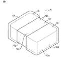
- FIG. 1 is a perspective schematic perspective view showing the internal structure of the surface mount inductor A.
- the surface-mount inductor A includes a resin molded body 12 having a substantially rectangular parallelepiped shape and external terminals 15 and 15 formed at both ends thereof.
- the resin molded body 12 has an upper surface 12c and a bottom surface 12d facing each other, and four side surfaces 12e, 12f, 12g, and 12h adjacent to the upper surface 12c and the bottom surface 12d.
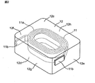
- FIG. 2 is a perspective schematic perspective view showing the structure of the resin molded body 12 and shows a state before the external terminals of FIG. 1 are formed.
- the coil 11 has a so-called “outer / outer winding” winding portion 11a in which a conductive wire is wound so that both ends thereof are positioned in opposite directions along the outer peripheral surface of the coil, and both ends of the winding portion 11a. It is a coil provided with a pair of drawer
- FIG. 2 shows an example of two-stage outer and outer windings. A pair of lead-out ends 11b and 11b of the coil 11 are exposed at the opposing first side surface 12e and second side surface 12f, which are located in the length direction of the resin molded body 12, respectively.
- the plating layer mentioned later is formed in the whole surface of the 1st side surface 12e and the 2nd side surface 12f including the exposed surface of the drawer
- a pair of conductive paste layers 14 and 14 formed by solidifying the conductive paste covering the five surfaces of 12h are formed.
- the leading end portions 11b and 11b at both ends of the coil 11 are connected to the pair of conductive paste layers 14 and 14 via plating layers, respectively.
- the plating layer and the conductive paste layer constitute the external terminals 15 and 15.
- the 1st side surface and 2nd side surface which oppose in a resin molding are opposing side surfaces, Comprising: The side surface where the straight line which connects the drawer
- FIG. 2 shows an elliptical coil in a top view, but is not limited thereto, and the shape of the coil may be a circular shape or a substantially rectangular shape in a top view.
- the lead-out end portions 11b and 11b are exposed at the first side surface 12e and the second side surface 12f, respectively, but the exposed area is not particularly limited as long as electrical connection with an external terminal is possible.
- drawing-out edge part may protrude from the 1st side surface and the 2nd side surface to such an extent that formation of the plating layer formed on it is not inhibited.
- the resin molded body contains metal magnetic powder, a binder resin, and additives such as a moldability improver and a release agent as necessary.
- the metal magnetic powder include iron-based metal magnetic powders such as Fe, Fe-Si-Cr, Fe-Si-Al, Fe-Ni-Al, and Fe-Cr-Al, and metal magnetism such as amorphous. Examples thereof include body powder, metal magnetic powder whose surface is coated with an insulator such as glass, and metal magnetic powder whose surface is modified.
- the binder resin include thermosetting resins such as epoxy resins, polyimide resins, and phenol resins, and thermoplastic resins such as polyethylene resins and polyamide resins.
- FIG. 2 although the case where the resin molding has a rectangular parallelepiped shape was shown, other rectangular body shapes, for example, a cube shape, may be sufficient.
- the surface mount inductor A can be manufactured using, for example, the following manufacturing method. That is, the manufacturing method is a method for manufacturing a surface mount inductor in which at least one coil is embedded in a resin molded body containing metal magnetic powder, and the at least one coil is disposed in a molding die. A molding step of filling the molding die material into the molding die to obtain the resin molding, wherein at least a part of the drawn end portions at both ends of the coil is on the surface of the resin molding.
- the step of forming the external terminal forms a first plating layer across the exposed portion of the metal magnetic powder and the exposed surface of the lead-out end.
- a step and the first Conductive paste on top of Tsu Ki layer contains at least a step of forming a conductive paste layer was solidified.
- At least one coil is disposed in a molding die, a resin molding material is filled in the molding die, and a rectangular body shape having opposing top and bottom surfaces and four side surfaces is formed.
- the winding part 11a is formed at both ends of the conducting wire.
- the coil 11 is formed by pulling out in the opposite direction from the outer periphery of the winding portion to form the pull-out end portions 11b and 11b at both ends.
- the resin used for the insulating coating preferably has a high heat resistance temperature, and examples thereof include polyamide resins, polyester resins, and imide-modified polyurethane resins. Moreover, not only a rectangular conductor with a flat cross section but also a round wire or a polygonal cross section can be used as the conductor.
- iron-based metal magnetic powders such as Fe, Fe—Si—Cr, Fe—Si—Al, Fe—Ni—Al, Fe—Cr—Al, and amorphous metal magnetic materials
- an epoxy resin is used as a binder resin, and these are mixed to produce a sealing material (resin molded body material).
- the coil 11 is placed in a predetermined molding die, and a resin molding material is filled in the die and compression molded.
- the drawing end portions at both ends of the coil By arranging the coil in the mold so that at least a part of the drawing end portions at both ends of the coil is exposed at the first side surface and the second side surface facing the resin molded body, respectively, the drawing end portions at both ends of the coil
- the resin molded body 12 in which at least a part of the resin molded body is exposed on the first side surface and the second side surface facing each other can be molded.
- the molding method is not limited to the compression molding method, and a powder molding method can also be used.
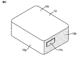
- the metal magnetic substance powder exposed portion 12b is formed on the entire surface of the first side face 12e and the second side face 12f.
- the metal magnetic substance powder exposed portion 12b has at least the leading end portions 11b at both ends. , 11b may be formed around the exposed surface.
- plating is performed on the exposed surfaces of the leading end portions 11b and 11b at both ends and the exposed metal magnetic powder portion 12b to form a plating layer 13 as shown in FIG.
- the plating layer 13 is formed on the entire first side surface 12e and the second side surface 12f. Thereby, the lead-out end portions 11 b and 11 b are connected to the plating layer 13.
- the conductive material used for the plating process is not particularly limited as long as it can be plated.
- a material containing at least one metal material selected from the group consisting of Cu, Ni, and Sn can be used.
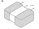
- the conductive paste is applied across the first side surface 12e and the four surfaces of the top surface 12c, the bottom surface 12d, the third side surface 12g, and the fourth side surface 12h adjacent to the first side surface 12e. Further, the conductive paste is applied across the second side surface 12f and the four surfaces of the upper surface 12c, the bottom surface 12d, the third side surface 12e, and the fourth side surface 12f adjacent to the second side surface 12f. Thereafter, heat treatment is performed to dry and solidify the conductive paste to form the conductive paste layers 14 and 14, thereby forming the external terminals 15 and 15. Thereby, the surface mount inductor A shown in the schematic perspective view of FIG. 5 is obtained.
- the conductive paste a paste in which metal particles such as Au and Ag are dispersed in a thermosetting resin such as an epoxy resin can be used.
- FIG. 6 is a partially cutaway schematic cross-sectional view of the obtained surface mount inductor A.
- the surface of the leading end portion 11b is exposed on the first side surface 12e.
- a plating layer 13 is formed so as to cover the surface of the leading end portion 11b and the exposed metal magnetic substance powder portion 12b. Further, the plating layer 13 is covered with a conductive paste layer 14.
- the external terminal 15 includes a plating layer 13 and a conductive paste layer 14.
- the metal magnetic powder exposed portion is formed at least around the exposed surface of the coil drawing end portion, it is easy for the plating to grow on the metal magnetic powder exposed portion, and the drawing end portion And the plating layer can be firmly bonded.
- the bonding area between the conductive paste layer and the leading end can be increased via the plating layer, not only the bonding strength between the leading end and the external terminal, but also the resin molded body and the external terminal Bonding strength can also be increased, and the external terminals can be prevented from peeling off due to thermal shock or physical stress. As a result, it is possible to provide a surface mount inductor having an external terminal with high connection reliability.
- the external terminal when forming the external terminal, it is only necessary to expose the metal magnetic powder on the exposed side surface of the lead end of the coil. Therefore, a method in which the metal magnetic powder on the other surface needs to be exposed, for example, L In the case of a letter-shaped external terminal, the workability of the external terminal can be improved.
- Embodiment 2 The surface mount inductor according to the present embodiment is the same as that of the first embodiment, except that the metal magnetic powder is exposed only around the exposed surface of the lead end portion on the exposed side surface of the lead end portion of the coil. It has a structure. Although description will be given with reference to FIGS. 7 to 9, the description of the parts common to the surface mount inductor of the first embodiment will be omitted.
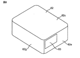
- FIG. 7 is a schematic perspective view in one manufacturing process of the surface-mount inductor B according to the present embodiment.
- FIG. 8 is a schematic perspective view in one manufacturing process of the surface mount inductor B.
- FIG. 9 is a schematic perspective view of the surface mount inductor B.
- the resin molded body 62 has an upper surface 62c and a bottom surface 62d facing each other, and four side surfaces 62e, 62f, 62g, and 62h that are in direct contact with the upper surface 62c and the bottom surface 62d.
- the drawn end portions 61b and 61b at both ends of the coil 61 are exposed on the first side surface 62e and the second side surface 62f, which are side surfaces facing each other in the length direction of the resin molded body 62.
- Metal magnetic powder exposed portions 62b and 62b are formed around the exposed surfaces of the drawer end portions 61b and 61b at both ends.
- a plating layer 63 is formed across the exposed surface of the lead-out end portion 61b of the coil 61 and the metal magnetic substance powder exposed portion 62b.
- a conductive paste layer is formed in an L shape across the first side surface 62e and the bottom surface 62d, and the external terminal 65 is formed. Further, an L-shaped conductive paste layer is formed across the second side surface 62f and the bottom surface 62d to form the external terminal 65. Thereby, the drawer
- the same effect as in the first embodiment can be obtained. Furthermore, since it is sufficient to remove the resin component only around the exposed surface of the drawer end, the workability of the external terminal can be further improved.
- Embodiment 3 The surface mount inductor according to the present embodiment has the same structure as that of the first embodiment except that a mesh-structured plating layer is used. Although description will be made with reference to FIGS. 10A to 10B, description of portions common to the surface-mount inductor of Embodiment 1 is omitted.
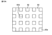
- FIG. 10A is a schematic side view in one manufacturing process of the surface-mount inductor C according to the present embodiment, and shows a state before the external terminals are formed.
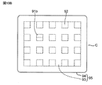
- FIG. 10B is a perspective schematic side view of the surface-mount inductor C.
- the lead-out end 91b is exposed on the first side surface 92e of the resin molded body 92.
- a plating layer 93 having a mesh structure is formed on the entire surface of the first side surface 92e.
- a conductive paste layer 94 is formed so as to cover the plating layer 93.
- the external terminal 94 is formed across the first side surface 92e and four surfaces adjacent to the first side surface 92e.
- the conductive paste layer 94 is bonded to the lead-out end portion 91b through the plating layer 93.
- the plating layer 93 having a mesh structure is formed by removing the resin component on the surface of the first side surface 92e into a mesh shape by laser irradiation to form a metal magnetic powder exposed portion having a mesh structure, and performing a plating process. Can be formed.
- a mesh-structured plating layer is also formed on the entire surface of the second side surface facing the first side surface 92e, and on the plating layer, adjacent to the second side surface and the second side surface.
- a conductive paste layer is formed across the four surfaces.
- the same effect as in the first embodiment can be obtained. Furthermore, the bonding strength between the resin molded body and the external terminal can be further improved by the anchor effect of the conductive paste that has entered the gap of the mesh structure of the plating layer 93.
- Embodiment 4 The surface mount inductor according to the present embodiment has the same structure as that of the first embodiment except that a plated layer having a slit structure is used. Although description will be given with reference to FIG. 11A to FIG. 11B, description of portions common to the surface-mount inductor of Embodiment 1 is omitted.
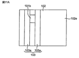
- FIG. 11A is a schematic side view in one manufacturing process of the surface-mount inductor D according to the present embodiment, and shows a state before the external terminals are formed.
- FIG. 11B is a perspective schematic side view of the surface-mount inductor D.
- the leading end portion 101b is exposed on the first side surface 102e of the resin molded body 102.
- a plating layer 103 having a slit structure is formed on the entire first side surface 102e.
- the conductive paste layer 104 is formed so that the plating layer 103 may be covered.
- the external terminal 104 is formed across the first side surface 102e and four surfaces adjacent to the first side surface 102e. As a result, the conductive paste layer 104 is bonded to the lead-out end portion 101 b through the plating layer 103.
- the plating layer 103 having the slit structure is formed by removing the resin component on the surface of the first side surface 102e into a slit shape by laser irradiation, and the metal magnetism of the plurality of protrusions extending in the lateral direction of the first side surface 102e.
- the body powder exposed portion By forming the body powder exposed portion and performing a plating process, it is possible to form a plating layer 103 in which a plurality of protrusion platings 103a are arranged in the lateral direction of the first side surface 102e.
- a plated layer having a slit structure is also formed on the entire surface of the second side surface facing the first side surface 102e, and on the plated layer, adjacent to the second side surface and the second side surface. External terminals are formed across the four surfaces.
- the same effect as in the first embodiment can be obtained. Furthermore, the bonding strength between the resin molded body and the external terminal can be further improved by the anchor effect of the conductive paste that has entered the gap of the slit structure of the plating layer 103.
- Embodiment 5 The surface mount inductor according to the present embodiment has the same structure as that of the first embodiment except that a plated layer having a slit structure is used. Although description will be made with reference to FIGS. 12A to 12B, description of portions common to the surface-mount inductor of Embodiment 1 is omitted.
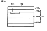
- FIG. 12A is a schematic side view in one manufacturing process of the surface-mount inductor E according to the present embodiment, and shows a state before the external terminals are formed.
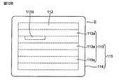
- 12B is a perspective schematic side view of the surface-mount inductor E.
- the leading end 111b is exposed on the first side surface 112e of the resin molded body 112.
- a plating layer 113 having a slit structure is formed on the entire surface of the first side surface 112e.
- a conductive paste layer 114 is formed so as to cover the plating layer 113.
- the conductive paste layer 114 is formed across the first side surface 112e and four surfaces adjacent to the first side surface 112e. As a result, the conductive paste layer 114 is bonded to the lead-out end portion 111b through the plating layer 113.
- the plating layer 113 having a slit structure removes the resin component on the surface of the first side surface 112e into a slit shape by laser irradiation, and the metal magnetism of the plurality of protrusions extending in the lateral direction of the first side surface 112e.
- the plating layer 113 By forming the body powder exposed portion and performing the plating process, it is possible to form the plating layer 113 in which a plurality of strip-like plating layers 113a are arranged in the vertical direction of the first side surface 112e.
- a plating layer having a slit structure is formed on the second side surface facing the first side surface 112e, and the second side surface and 4 adjacent to the second side surface are further formed on the plating layer.
- a conductive paste layer is formed across the two surfaces.
- the same effect as in the first embodiment can be obtained. Furthermore, the bonding strength between the resin molded body and the external terminal can be further improved by the anchor effect of the conductive paste that has entered the gap of the slit structure of the plating layer 113.
- Embodiment 6 The surface mount inductor according to the present embodiment is the same as that of the first embodiment except that the plating layers are formed in the vertical direction of the first side surface and the second side surface so as to overlap at least a part of the exposed surface of the lead-out end portion. It has the same structure. Although description will be made with reference to FIGS. 13A to 13B, description of portions common to the surface-mount inductor of Embodiment 1 is omitted.
- FIG. 13A is a schematic side view in one manufacturing process of the surface-mount inductor F according to the present embodiment, and shows a state before the external terminals are formed.
- FIG. 13B is a perspective schematic side view of the surface-mount inductor F.
- the lead-out end 121b is exposed on the first side surface 122e of the resin molded body 122.
- the plating layer 123 is formed in the vertical direction of the 1st side surface 122e so that it may overlap with the approximate center part of the exposed surface of the drawer
- a conductive paste layer 124 is formed so as to cover the plating layer 123.
- the conductive paste layer 124 is formed across the first side surface 122e and four surfaces adjacent to the first side surface 122e. Thereby, the conductive paste layer 124 is joined to the lead-out end part 121b through the plating layer 123.
- a plating layer is formed in the vertical direction of the second side surface on the second side surface facing the first side surface 122e so as to overlap with the substantially central portion of the exposed surface of the drawer end,
- external terminals are formed across the second side surface and four surfaces adjacent to the second side surface.
- 13A and 13B show an example in which the plating layer 123 is formed in the vertical direction of the first side surface 122e so as to overlap the substantially central portion of the exposed surface of the leading end 121b. Need only overlap with at least part of the exposed surface of the drawer end 121b.
- the same effect as in the first embodiment can be obtained. Furthermore, by forming the plating layer directly on the exposed surface of the leading end, the bonding strength between the plating layer and the leading end can be further improved.
- the external terminal includes a first plating layer, a conductive paste layer, and a second plating layer formed on the conductive paste layer.
- Embodiment 1 except that the conductive paste layer has one conductive paste layer non-formation region, and the first plating layer and the second plating layer are directly bonded in the conductive paste layer non-formation region. It has the same structure. Although described with reference to FIG. 14, description of portions common to the surface mount inductor of the first embodiment is omitted.
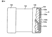
- FIG. 14 is a partially cutaway schematic cross-sectional view of the surface mount inductor G according to the present embodiment.
- the external terminal 135 includes a first plating layer 133a, a conductive paste layer 134, and a second plating layer 133b.
- a first plating layer 133a is formed on the leading end 131b, and a conductive paste layer 134 having one conductive paste layer non-formation region 134a is formed on the first plating layer 133a.
- a second plating layer 133 b is formed on the conductive paste layer 134 so as to cover the conductive paste layer 134.
- the first plating layer 133a and the second plating layer 133b are directly joined at a conductive paste layer non-formation region 134a provided substantially at the center of the first plating layer 133a.
- the first plating layer 133a is formed on the entire surface of the first side surface 132e.
- the conductive paste layer 134 is formed across the first side surface 132e and four surfaces adjacent to the first side surface 132e.
- a metal material such as Cu, Ni, or Sn can be used for the plating layer, it is preferable to use Cu for the first plating layer and Ni for the second plating layer.
- the external terminals are also formed on the first plating layer, the conductive paste layer, and the second paste layer formed on the conductive paste layer on the second side surface facing the first side surface 132e.
- the conductive paste layer has one conductive paste layer non-formation region, and the first plating layer and the second plating layer are directly joined in the conductive paste layer non-formation region. ing.
- the conductive paste layer non-formation region can be formed by applying using a predetermined mask pattern.
- region extended in the horizontal direction of the 1st plating layer 133a can be used for an electroconductive paste layer non-formation area
- the same effect as in the first embodiment can be obtained.
- the conductive paste layer is sandwiched between the first plating layer and the second plating layer, and the first plating layer and the second plating layer are directly joined in the conductive paste layer non-formation region, thereby providing conductivity. It becomes possible to improve the adhesiveness of the paste layer to the resin molded body, and further improve the connection reliability.
- the example in which the first plating layer 133a is formed on the substantially entire surface of the first side surface 132e is shown, but the mesh structure described in the third to fifth embodiments is used.
- a plating layer having a slit structure can be used. This case also has the same effect as the present embodiment.
- a conductive paste layer is formed so that the conductive paste layer covers the first plating layer 133a around the first side surface that is exposed, and a second plating layer is formed on the conductive paste layer.
- the first plating layer and the second plating layer can be directly joined. This case also has the same effect as the present embodiment.
- the conductive paste layer has a plurality of conductive paste layer non-formation regions, and the first plating layer and the second plating are formed in the plurality of conductive paste layer non-formation regions.
- the structure is the same as that of Embodiment 7 except that the layers are directly bonded.
- FIG. 15 is a partially cutaway schematic cross-sectional view of the surface mount inductor H according to the present embodiment.
- the leading end portion 141b is exposed on the first side surface 142e of the resin molded body 142.
- the external terminal 145 includes a first plating layer 143a, a conductive paste layer 144, and a second plating layer 143b.
- a first plating layer 143a is formed on the leading end portion 141b, and a conductive paste layer 144 having a plurality of conductive paste layer non-forming regions 144a is formed on the first plating layer 143a.
- a second plating layer 143b is formed on the conductive paste layer 144 so as to cover the conductive paste layer 144.
- the first plating layer 143a and the second plating layer 143b are directly bonded to each other at a conductive paste layer non-formation region 144a arranged in the vertical direction of the first plating layer 143a.
- a strip-like region extending in the lateral direction of the first plating layer 143a can be used for each conductive paste layer non-formation region.
- the same effect as in the seventh embodiment can be obtained. Furthermore, by directly joining the first plating layer and the second plating layer in a plurality of conductive paste layer non-formation regions, it becomes possible to further improve the adhesion of the conductive paste layer to the resin molded body, Furthermore, connection reliability can be improved.
- the example in which the first plating layer 143a is formed on the substantially entire surface of the first side surface 142e is shown.
- the mesh structure described in the third to fifth embodiments is used.
- a plating layer having a slit structure can be used. This case also has the same effect as the present embodiment.
- a conductive paste layer is formed so that the conductive paste layer covers the first plating layer 143a on the first side surface that is exposed, and a second plating layer is formed on the conductive paste layer.
- the first plating layer and the second plating layer can be directly joined. This case also has the same effect as the present embodiment.
- Embodiment 9 The surface mount inductor according to the present embodiment is the same as that of the first embodiment except that the conductive paste layer is formed on the upper and lower edges of the plating layer and the four surfaces adjacent to the first side surface. It has the structure of. A description will be given with reference to FIG. 16, but a description of portions common to the surface mount inductor of the first embodiment will be omitted.
- FIG. 16 is a partially cutaway schematic cross-sectional view of the surface mount inductor I according to the present embodiment.
- the leading end 151b is exposed on the first side surface 152e of the resin molded body 152.
- a plating layer 153 is formed on the leading end 141b.
- a conductive paste layer 154 is formed on the upper and lower edges of the plating layer 153 and on the four surfaces adjacent to the first side surface.
- the same effect as in the first embodiment can be obtained. Furthermore, since the conductive paste layer is formed on the upper edge and the lower edge of the plating layer instead of the entire surface of the plating layer, the amount of expensive conductive paste used can be reduced.
- Embodiment 10 In the surface mount inductor according to the present embodiment, the lead end portion of the coil is pulled out from the first side surface, and the leading end portion is bent so as to be in contact with the exposed portion of the metal magnetic powder formed on the first side surface.
- the bent portion has a structure similar to that of the first embodiment except that the bent end portion is fixed to the resin molded body and the insulating coating of the bent portion is removed to form a plating layer. is doing.
- the same effect as in the seventh embodiment can be obtained. Furthermore, by forming a plating layer in the bent portion, the bonding area can be increased, and the bonding strength can be further improved. Further, since the tolerance for the arrangement of the lead-out end portion is larger during the production of the resin molded body than in the case where the coil is exposed to the first side surface of the lead-out end portion, the effect of facilitating the production of the resin molded body can be obtained. .
- the bent end portion can be formed by pulling out the lead end portion of the coil from the first side surface. This case also has the same effect as the present embodiment.
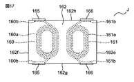
- Embodiment 11 is an example of a surface mount inductor J in which two coils are embedded in a resin molded body. 17, 18, and 19 show a perspective schematic top view, a schematic side view, and a schematic bottom view of the surface-mount inductor J, respectively.
- two coils 160 and 161 around which conductive wires are wound are embedded in the length direction of the resin molded body 162.
- One coil 160 has a winding portion 160a in which the conductive wire is wound so that both ends thereof are positioned in opposite directions along the outer peripheral surface of the coil, and a non-winding portion provided at both ends of the winding portion 160a. It is a coil provided with a pair of drawer
- the other coil 161 includes a winding portion 161a and a pair of lead-out end portions 161b and 161b each having a non-winding portion provided at both ends of the winding portion 161a.
- the length direction of the resin molding in this Embodiment refers to the direction where the straight line which cross
- a pair of leading end portions 160b and 160b of the coil 160 are exposed to the opposing third side surface 162g and fourth side surface 12h, which are located in the width direction of the resin molded body 162, while a pair of leading end portions of the coil 161 are exposed. 161b and 161b are also exposed.
- a plating layer (not shown) is formed across the exposed surfaces of the leading end portions 160b and 160b, the third side surface 162g, and a part of the fourth side surface 162h.
- a pair of conductive paste layers (not shown) formed by solidifying the conductive paste extending in a band shape on the upper surface 162c and the side surfaces 162g and 162h of the resin molded body 162 and reaching the bottom surface 162d.
- plating layers are respectively formed across the exposed surfaces of the lead-out end portions 161b and 161b, the third side surface 162g, and a part of the fourth side surface 162h.
- a pair of conductive paste layers (not shown) formed by solidifying the conductive paste extending in a band shape on the upper surface 162c and the side surfaces 162g and 162h of the resin molded body 162 and reaching the bottom surface 162d. Is formed.
- the leading end portions 160b and 160b at both ends of the coil 160 are connected to the pair of conductive paste layers through the plating layers, respectively.
- the plating layer and the conductive paste layer constitute a pair of external terminals 165 and 165.
- the lead-out end portions 161b and 161b at both ends of the coil 161 are connected to a pair of conductive paste layers through a plating layer, respectively, and the plating layer and the conductive paste layer constitute a pair of external terminals 166 and 166.
- the third side surface 162g and the fourth side surface 162h are opposite side surfaces, and mean the side surfaces where the straight lines connecting the leading end portions at both ends of the coil intersect.
Landscapes
- Engineering & Computer Science (AREA)
- Power Engineering (AREA)
- Manufacturing & Machinery (AREA)
- Microelectronics & Electronic Packaging (AREA)
- Coils Or Transformers For Communication (AREA)
- Manufacturing Cores, Coils, And Magnets (AREA)
Abstract
Description
本実施の形態に係る表面実装インダクタは、金属磁性体粉末を含む樹脂成形体と、少なくとも1つのコイルであって、該コイルの両端の引き出し端部の少なくとも一部が、前記樹脂成形体の表面に露出するように前記樹脂成形体に埋設された該コイルと、前記引き出し端部の露出面と該露出面の少なくとも周囲に形成された金属磁性体粉末露出部とに跨がって形成された外部端子と、を有し、前記外部端子が、金属磁性体粉末露出部と前記の引き出し端部の露出面とに跨がって形成された第1のめっき層と、該第1のめっき層の上に形成された、導電性ペーストが固化した導電性ペースト層とを少なくとも含むことを特徴とするものである。
本工程は、少なくとも1つのコイルを成形用金型内に配置し、樹脂成形体用材料を成形用金型内に充填して、対向する上面と底面、および4つの側面を有する矩形体形状を有する、前記樹脂成形体を得る成形工程であって、前記コイルの両端の引き出し端部の少なくとも一部が、対向する第1側面と第2側面でそれぞれ露出するように前記コイルを前記樹脂成形体内に埋設する。
コイル11の両端の引き出し端部11b,11bの表面の被膜を機械剥離によって除去する。その後、図3に示す様に、樹脂成形体12の対向する第1側面12eと第2側面12fの表面に存在する樹脂成分をレーザー照射、ブラスト処理、研磨等を用いて除去する。これにより、両端の引き出し端部11b,11bの露出面以外の第1側面12eと第2側面12fに、樹脂成形体12を構成する金属磁性体粉末が露出した金属磁性体粉末露出部12bを形成する。図3では、金属磁性体粉末露出部12bを、第1側面12eと第2側面12fの全面に形成した例を示したが、金属磁性体粉末露出部12bは、少なくとも、両端の引き出し端部11b,11bの露出面の周囲に形成されていればよい。
本実施の形態に係る表面実装インダクタは、コイルの引き出し端部の露出した側面において、引き出し端部の露出面の周囲のみに金属磁性体粉末を露出させた以外は、実施の形態1と同様の構造を有している。図7~図9を参照して説明するが、実施の形態1の表面実装インダクタと共通する部分については説明を省略する。
本実施の形態に係る表面実装インダクタは、メッシュ構造のめっき層を用いた以外は、実施の形態1と同様の構造を有している。図10A~図10Bを参照して説明するが、実施の形態1の表面実装インダクタと共通する部分については説明を省略する。
本実施の形態に係る表面実装インダクタは、スリット構造のめっき層を用いた以外は、実施の形態1と同様の構造を有している。図11A~図11Bを参照して説明するが、実施の形態1の表面実装インダクタと共通する部分については説明を省略する。
本実施の形態に係る表面実装インダクタは、スリット構造のめっき層を用いた以外は、実施の形態1と同様の構造を有している。図12A~図12Bを参照して説明するが、実施の形態1の表面実装インダクタと共通する部分については説明を省略する。
本実施の形態に係る表面実装インダクタは、引き出し端部の露出面の少なくとも一部と重なるように、第1側面および第2側面の縦方向にめっき層を形成した以外は、実施の形態1と同様の構造を有している。図13A~図13Bを参照して説明するが、実施の形態1の表面実装インダクタと共通する部分については説明を省略する。
本実施の形態に係る表面実装インダクタは、外部端子が、第1のめっき層と、導電性ペースト層と、該導電性ペースト層の上に形成された第2のめっき層とを含むとともに、導電性ペースト層が1の導電性ペースト層非形成領域を有し、該導電性ペースト層非形成領域で第1のめっき層と第2のめっき層が直接接合している以外は、実施の形態1と同様の構造を有している。図14を参照して説明するが、実施の形態1の表面実装インダクタと共通する部分については説明を省略する。
本実施の形態に係る表面実装インダクタは、導電性ペースト層が複数の導電性ペースト層非形成領域を有し、該複数の導電性ペースト層非形成領域で第1のめっき層と第2のめっき層が直接接合している以外は、実施の形態7と同様の構造を有している。
本実施の形態に係る表面実装インダクタは、導電性ペースト層を、めっき層の上方縁部と下方縁部、および第1側面と隣接する4つの面に形成した以外は、実施の形態1と同様の構造を有している。図16を参照して説明するが、実施の形態1の表面実装インダクタと共通する部分については説明を省略する。
本実施の形態に係る表面実装インダクタは、コイルの引き出し端部を第1側面から引き出して、引き出した先端部を、第1側面上に形成した金属磁性体粉末露出部に接するように折り曲げて折り曲げ部を形成し、この折り曲げ部により引き出し端部を樹脂成形体に固定した状態で、その折り曲げ部の絶縁被覆を除去してめっき層を形成した以外は、実施の形態1と同様の構造を有している。
本実施の形態は、2つのコイルを樹脂成形体に埋設した表面実装インダクタJの一例である。図17,18,19は、それぞれ、表面実装インダクタJの透視模式上面図、模式側面図、および模式底面図を示す。
11a,61a,160a,161a 巻回部
11b,61b,91b,101b,111b,121b,131b,141b,151b,160b,161b 引き出し端部
12,62,92,102,112,122,132,142,152,
162 樹脂成形体
12b,62b 金属磁性体粉末露出部
12c,62c,162c 上面
12d,62d,162d 底面
12e,62e,92e,102e,112e,122e,132e,142e,162e 第1側面
12f,62f,162f 第2側面
12g,62g,162g 第3側面
12h,62h,162h 第4側面
13,63,93,113,123,153,103a,113a
めっき層
133a,143a, 第1のめっき層
133b,143b 第2のめっき層
14,94,104,114,124,134,144,154
導電性ペースト層
134a,144a 導電性ペースト層非形成領域
15,65,95,105,115,125,135,145,155,165,166 外部端子
Claims (15)
- 金属磁性体粉末を含む樹脂成形体と、
少なくとも1つのコイルであって、該コイルの両端の引き出し端部の少なくとも一部が、前記樹脂成形体の表面に露出するように前記樹脂成形体に埋設された該コイルと、
前記引き出し端部の露出面と該露出面の少なくとも周囲に形成された金属磁性体粉末露出部とに跨がって形成された外部端子と、を有し、
前記外部端子が、金属磁性体粉末露出部と前記の引き出し端部の露出面とに跨がって形成された第1のめっき層と、該第1のめっき層の上に形成された、導電性ペーストが固化した導電性ペースト層とを少なくとも含む、表面実装インダクタ。 - 前記外部端子が、前記第1のめっき層と、前記導電性ペースト層と、前記導電性ペースト層の上に形成された第2のめっき層とを含む、請求項1記載の表面実装インダクタ。
- 前記導電性ペースト層が1つ以上の導電性ペースト層非形成領域を有し、該導電性ペースト層非形成領域で前記第1のめっき層と前記第2のめっき層が直接接合している、請求項2記載の表面実装インダクタ。
- 前記樹脂成形体が、対向する上面と底面、および4つの側面を有する矩形体形状を有し、前記両端の引き出し端部の各引き出し端部が、対向する第1側面と第2側面にそれぞれ露出している、請求項1から3のいずれか1項に記載の表面実装インダクタ。
- 前記金属磁性体粉末露出部が、前記の引き出し端部の露出面以外の前記第1側面と前記第2側面の全面に形成され、前記第1のめっき層と前記導電性ペースト層が、前記の引き出し端部の露出面を含む前記第1側面と前記第2側面の全面に形成されている、請求項4に記載の表面実装インダクタ。
- 前記コイルの両端の前記引き出し端部が、前記対向する第1側面と第2側面から引き出されている請求項4または5に記載の表面実装インダクタ。
- 前記第1のめっき層がメッシュ構造を有する請求項1から6のいずれか1項に記載の表面実装インダクタ。
- 前記第1のめっき層がスリット構造を有する請求項1から6のいずれか1項に記載の表面実装インダクタ。
- 少なくとも1つのコイルが、金属磁性体粉末を含む樹脂成形体に埋設されている表面実装インダクタの製造方法であって、
前記少なくとも1つのコイルを成形用金型内に配置し、樹脂成形体用材料を前記成形用金型内に充填して前記樹脂成形体を得る成形工程であって、前記コイルの両端の引き出し端部の少なくとも一部が前記樹脂成形体の表面に露出するように前記コイルを前記樹脂成形体内に埋設する該成形工程と、
前記引き出し端部の露出面と該露出面の少なくとも周囲に形成された金属磁性体粉末露出部とに跨がる外部端子を形成する工程と、を有し、
前記の外部端子を形成する工程が、前記金属磁性体粉末露出部と前記の引き出し端部の露出面とに跨がって第1のめっき層を形成する工程と、該第1のめっき層の上に導電性ペーストが固化した導電性ペースト層を形成する工程を少なくとも含む、該表面実装インダクタの製造方法。 - 前記樹脂成形体が、対向する上面と底面、および4つの側面を有する矩形体形状を有し、前記成形工程において、前記両端の引き出し端部の各引き出し端部が、対向する第1側面と第2側面にそれぞれ露出するように前記樹脂成形体を成形する、請求項9に記載の製造方法。
- 前記金属磁性体粉末露出部を、前記の引き出し端部の露出面以外の前記第1側面と前記第2側面の全面に形成する、請求項10記載の製造方法。
- 前記の外部端子を形成する工程が、前記導電性ペースト層の上に第2のめっき層を形成する工程を含む、請求項9から11のいずれか1項に記載の製造方法。
- 前記導電性ペースト層に1つ以上の導電性ペースト層非形成領域を形成し、該導電性ペースト層非形成領域で前記第1のめっき層と前記第2のめっき層とを直接接合させる、請求項12記載の製造方法。
- 前記の第1のめっき層を形成する工程において、メッシュ構造の前記第1のめっき層を形成する、請求項9から13のいずれか1項に記載の製造方法。
- 前記の第1のめっき層を形成する工程において、スリット構造の前記第1のめっき層を形成する、請求項9から13のいずれか1項に記載の製造方法。
Priority Applications (5)
| Application Number | Priority Date | Filing Date | Title |
|---|---|---|---|
| JP2017558899A JP6460264B2 (ja) | 2015-12-28 | 2016-11-30 | 表面実装インダクタ及びその製造方法 |
| KR1020187018016A KR102077952B1 (ko) | 2015-12-28 | 2016-11-30 | 표면 실장 인덕터 및 그 제조 방법 |
| CN201680076180.9A CN108431911B (zh) | 2015-12-28 | 2016-11-30 | 表面安装电感器及其制造方法 |
| US16/019,399 US11456114B2 (en) | 2015-12-28 | 2018-06-26 | Surface-mount inductor and manufacturing method thereof |
| US17/820,196 US12597553B2 (en) | 2015-12-28 | 2022-08-16 | Manufacturing method of surface-mount inductor |
Applications Claiming Priority (2)
| Application Number | Priority Date | Filing Date | Title |
|---|---|---|---|
| JP2015-256012 | 2015-12-28 | ||
| JP2015256012 | 2015-12-28 |
Related Child Applications (1)
| Application Number | Title | Priority Date | Filing Date |
|---|---|---|---|
| US16/019,399 Continuation US11456114B2 (en) | 2015-12-28 | 2018-06-26 | Surface-mount inductor and manufacturing method thereof |
Publications (1)
| Publication Number | Publication Date |
|---|---|
| WO2017115604A1 true WO2017115604A1 (ja) | 2017-07-06 |
Family
ID=59224978
Family Applications (1)
| Application Number | Title | Priority Date | Filing Date |
|---|---|---|---|
| PCT/JP2016/085626 Ceased WO2017115604A1 (ja) | 2015-12-28 | 2016-11-30 | 表面実装インダクタ及びその製造方法 |
Country Status (5)
| Country | Link |
|---|---|
| US (2) | US11456114B2 (ja) |
| JP (1) | JP6460264B2 (ja) |
| KR (1) | KR102077952B1 (ja) |
| CN (1) | CN108431911B (ja) |
| WO (1) | WO2017115604A1 (ja) |
Cited By (4)
| Publication number | Priority date | Publication date | Assignee | Title |
|---|---|---|---|---|
| JP2019036649A (ja) * | 2017-08-17 | 2019-03-07 | 株式会社村田製作所 | インダクタ |
| EP3480845A1 (en) * | 2017-11-07 | 2019-05-08 | Walsin Technology Corporation | Leadless electronic component and an encapsulation method thereof |
| JP2023154653A (ja) * | 2022-04-07 | 2023-10-20 | 株式会社村田製作所 | インダクタ |
| US12340931B2 (en) | 2022-03-30 | 2025-06-24 | Taiyo Yuden Co., Ltd | Coil component, circuit board arrangement, electronic device and method of manufacturing coil component |
Families Citing this family (8)
| Publication number | Priority date | Publication date | Assignee | Title |
|---|---|---|---|---|
| JP6673161B2 (ja) * | 2016-11-24 | 2020-03-25 | 株式会社村田製作所 | コイル部品 |
| JP6958525B2 (ja) * | 2018-09-25 | 2021-11-02 | 株式会社村田製作所 | インダクタ部品 |
| JP7124757B2 (ja) * | 2019-02-20 | 2022-08-24 | 株式会社村田製作所 | インダクタ |
| JP7188258B2 (ja) * | 2019-04-22 | 2022-12-13 | Tdk株式会社 | コイル部品及びその製造方法 |
| JP7322919B2 (ja) * | 2021-03-30 | 2023-08-08 | 株式会社村田製作所 | インダクタおよびインダクタの製造方法 |
| JP7384187B2 (ja) * | 2021-03-30 | 2023-11-21 | 株式会社村田製作所 | インダクタおよびインダクタの製造方法 |
| KR20230053181A (ko) * | 2021-10-14 | 2023-04-21 | 삼성전기주식회사 | 코일 부품 |
| KR102482949B1 (ko) * | 2022-02-15 | 2023-01-02 | 아비코전자 주식회사 | 인덕터 및 그 제조방법 |
Citations (3)
| Publication number | Priority date | Publication date | Assignee | Title |
|---|---|---|---|---|
| JP2001052937A (ja) * | 1999-08-13 | 2001-02-23 | Murata Mfg Co Ltd | インダクタ及びその製造方法 |
| WO2012105489A1 (ja) * | 2011-01-31 | 2012-08-09 | 東光株式会社 | 面実装インダクタと面実装インダクタの製造方法 |
| JP2014225590A (ja) * | 2013-05-17 | 2014-12-04 | 東光株式会社 | 面実装インダクタの製造方法 |
Family Cites Families (13)
| Publication number | Priority date | Publication date | Assignee | Title |
|---|---|---|---|---|
| JP3395759B2 (ja) * | 2000-04-12 | 2003-04-14 | 松下電器産業株式会社 | チップインダクタの製造方法 |
| JP2005116708A (ja) | 2003-10-06 | 2005-04-28 | Tdk Corp | チップインダクタ及びその製造方法 |
| JP5084459B2 (ja) * | 2007-11-15 | 2012-11-28 | 太陽誘電株式会社 | インダクタ及びその製造方法 |
| JP4714779B2 (ja) * | 2009-04-10 | 2011-06-29 | 東光株式会社 | 表面実装インダクタの製造方法とその表面実装インダクタ |
| JP4905498B2 (ja) * | 2009-04-22 | 2012-03-28 | 株式会社村田製作所 | 積層型セラミック電子部品 |
| US8299882B2 (en) * | 2009-07-22 | 2012-10-30 | Volterra Semiconductor Corporation | Low profile inductors for high density circuit boards |
| KR101872525B1 (ko) * | 2011-11-30 | 2018-08-03 | 삼성전기주식회사 | 인쇄회로기판 및 그 제조 방법 |
| JP5832355B2 (ja) | 2012-03-30 | 2015-12-16 | 東光株式会社 | 面実装インダクタの製造方法 |
| KR101688299B1 (ko) * | 2012-08-10 | 2016-12-20 | 가부시키가이샤 무라타 세이사쿠쇼 | 자성체 조성물 및 코일 부품 |
| JP2014067991A (ja) * | 2012-09-06 | 2014-04-17 | Toko Inc | 面実装インダクタ |
| KR20140038914A (ko) * | 2013-10-29 | 2014-03-31 | 삼성전기주식회사 | 적층 세라믹 커패시터 및 그 실장 기판 |
| US20150162122A1 (en) * | 2013-12-09 | 2015-06-11 | Joinset Co., Ltd. | Surface mount device type inductor and method of manufacturing the same |
| JP6179491B2 (ja) | 2014-09-05 | 2017-08-16 | 株式会社村田製作所 | 表面実装インダクタ及びその製造方法 |
-
2016
- 2016-11-30 JP JP2017558899A patent/JP6460264B2/ja active Active
- 2016-11-30 KR KR1020187018016A patent/KR102077952B1/ko active Active
- 2016-11-30 CN CN201680076180.9A patent/CN108431911B/zh active Active
- 2016-11-30 WO PCT/JP2016/085626 patent/WO2017115604A1/ja not_active Ceased
-
2018
- 2018-06-26 US US16/019,399 patent/US11456114B2/en active Active
-
2022
- 2022-08-16 US US17/820,196 patent/US12597553B2/en active Active
Patent Citations (3)
| Publication number | Priority date | Publication date | Assignee | Title |
|---|---|---|---|---|
| JP2001052937A (ja) * | 1999-08-13 | 2001-02-23 | Murata Mfg Co Ltd | インダクタ及びその製造方法 |
| WO2012105489A1 (ja) * | 2011-01-31 | 2012-08-09 | 東光株式会社 | 面実装インダクタと面実装インダクタの製造方法 |
| JP2014225590A (ja) * | 2013-05-17 | 2014-12-04 | 東光株式会社 | 面実装インダクタの製造方法 |
Cited By (5)
| Publication number | Priority date | Publication date | Assignee | Title |
|---|---|---|---|---|
| JP2019036649A (ja) * | 2017-08-17 | 2019-03-07 | 株式会社村田製作所 | インダクタ |
| EP3480845A1 (en) * | 2017-11-07 | 2019-05-08 | Walsin Technology Corporation | Leadless electronic component and an encapsulation method thereof |
| US12340931B2 (en) | 2022-03-30 | 2025-06-24 | Taiyo Yuden Co., Ltd | Coil component, circuit board arrangement, electronic device and method of manufacturing coil component |
| JP2023154653A (ja) * | 2022-04-07 | 2023-10-20 | 株式会社村田製作所 | インダクタ |
| JP7613409B2 (ja) | 2022-04-07 | 2025-01-15 | 株式会社村田製作所 | インダクタ |
Also Published As
| Publication number | Publication date |
|---|---|
| CN108431911B (zh) | 2020-10-23 |
| US20180308628A1 (en) | 2018-10-25 |
| US11456114B2 (en) | 2022-09-27 |
| JP6460264B2 (ja) | 2019-01-30 |
| US12597553B2 (en) | 2026-04-07 |
| KR20180085010A (ko) | 2018-07-25 |
| JPWO2017115604A1 (ja) | 2018-10-18 |
| KR102077952B1 (ko) | 2020-02-14 |
| CN108431911A (zh) | 2018-08-21 |
| US20220392694A1 (en) | 2022-12-08 |
Similar Documents
| Publication | Publication Date | Title |
|---|---|---|
| JP6460264B2 (ja) | 表面実装インダクタ及びその製造方法 | |
| JP3593986B2 (ja) | コイル部品及びその製造方法 | |
| JP6409328B2 (ja) | コイル部品 | |
| JP7124757B2 (ja) | インダクタ | |
| JP5832355B2 (ja) | 面実装インダクタの製造方法 | |
| JP6060116B2 (ja) | 表面実装インダクタ及びその製造方法 | |
| JP7052238B2 (ja) | コイル装置 | |
| JP6179491B2 (ja) | 表面実装インダクタ及びその製造方法 | |
| US20090160596A1 (en) | Magnetic device | |
| JP2014225590A (ja) | 面実装インダクタの製造方法 | |
| JP7132745B2 (ja) | 表面実装インダクタ | |
| JP2011216681A (ja) | コイル部品 | |
| JP6455561B2 (ja) | 電子部品 | |
| JP2016219781A (ja) | コイル電子部品及びその製造方法 | |
| WO2013018755A1 (ja) | コイル部品及びその製造方法 | |
| JP6323365B2 (ja) | 表面実装インダクタ及びその製造方法 | |
| JP5233558B2 (ja) | コイル部品 | |
| JP6409765B2 (ja) | 表面実装インダクタ | |
| JP2017191941A (ja) | 表面実装インダクタ及びその製造方法 | |
| JP6897619B2 (ja) | 表面実装インダクタおよびその製造方法 | |
| JP6379468B2 (ja) | 巻線型電子部品 | |
| KR101792279B1 (ko) | 인덕터 및 인덕터 제조 방법 | |
| WO2017115603A1 (ja) | 表面実装インダクタ及びその製造方法 | |
| JP2005217084A (ja) | インダクタ及びその製造方法 | |
| JP2008210978A (ja) | 巻線型電子部品 |
Legal Events
| Date | Code | Title | Description |
|---|---|---|---|
| 121 | Ep: the epo has been informed by wipo that ep was designated in this application |
Ref document number: 16881584 Country of ref document: EP Kind code of ref document: A1 |
|
| ENP | Entry into the national phase |
Ref document number: 2017558899 Country of ref document: JP Kind code of ref document: A |
|
| ENP | Entry into the national phase |
Ref document number: 20187018016 Country of ref document: KR Kind code of ref document: A |
|
| WWE | Wipo information: entry into national phase |
Ref document number: 1020187018016 Country of ref document: KR |
|
| NENP | Non-entry into the national phase |
Ref country code: DE |
|
| 122 | Ep: pct application non-entry in european phase |
Ref document number: 16881584 Country of ref document: EP Kind code of ref document: A1 |