WO2017002704A1 - はんだ材料、はんだ継手およびはんだ材料の検査方法 - Google Patents
はんだ材料、はんだ継手およびはんだ材料の検査方法 Download PDFInfo
- Publication number
- WO2017002704A1 WO2017002704A1 PCT/JP2016/068673 JP2016068673W WO2017002704A1 WO 2017002704 A1 WO2017002704 A1 WO 2017002704A1 JP 2016068673 W JP2016068673 W JP 2016068673W WO 2017002704 A1 WO2017002704 A1 WO 2017002704A1
- Authority
- WO
- WIPO (PCT)
- Prior art keywords
- core
- solder
- ball
- solder material
- oxide film
- Prior art date
Links
Images


Classifications
-
- B—PERFORMING OPERATIONS; TRANSPORTING
- B23—MACHINE TOOLS; METAL-WORKING NOT OTHERWISE PROVIDED FOR
- B23K—SOLDERING OR UNSOLDERING; WELDING; CLADDING OR PLATING BY SOLDERING OR WELDING; CUTTING BY APPLYING HEAT LOCALLY, e.g. FLAME CUTTING; WORKING BY LASER BEAM
- B23K35/00—Rods, electrodes, materials, or media, for use in soldering, welding, or cutting
- B23K35/02—Rods, electrodes, materials, or media, for use in soldering, welding, or cutting characterised by mechanical features, e.g. shape
- B23K35/0222—Rods, electrodes, materials, or media, for use in soldering, welding, or cutting characterised by mechanical features, e.g. shape for use in soldering, brazing
- B23K35/0244—Powders, particles or spheres; Preforms made therefrom
-
- B—PERFORMING OPERATIONS; TRANSPORTING
- B22—CASTING; POWDER METALLURGY
- B22F—WORKING METALLIC POWDER; MANUFACTURE OF ARTICLES FROM METALLIC POWDER; MAKING METALLIC POWDER; APPARATUS OR DEVICES SPECIALLY ADAPTED FOR METALLIC POWDER
- B22F1/00—Metallic powder; Treatment of metallic powder, e.g. to facilitate working or to improve properties
- B22F1/06—Metallic powder characterised by the shape of the particles
- B22F1/065—Spherical particles
-
- B—PERFORMING OPERATIONS; TRANSPORTING
- B22—CASTING; POWDER METALLURGY
- B22F—WORKING METALLIC POWDER; MANUFACTURE OF ARTICLES FROM METALLIC POWDER; MAKING METALLIC POWDER; APPARATUS OR DEVICES SPECIALLY ADAPTED FOR METALLIC POWDER
- B22F1/00—Metallic powder; Treatment of metallic powder, e.g. to facilitate working or to improve properties
- B22F1/10—Metallic powder containing lubricating or binding agents; Metallic powder containing organic material
- B22F1/102—Metallic powder coated with organic material
-
- B—PERFORMING OPERATIONS; TRANSPORTING
- B22—CASTING; POWDER METALLURGY
- B22F—WORKING METALLIC POWDER; MANUFACTURE OF ARTICLES FROM METALLIC POWDER; MAKING METALLIC POWDER; APPARATUS OR DEVICES SPECIALLY ADAPTED FOR METALLIC POWDER
- B22F1/00—Metallic powder; Treatment of metallic powder, e.g. to facilitate working or to improve properties
- B22F1/14—Treatment of metallic powder
- B22F1/142—Thermal or thermo-mechanical treatment
-
- B—PERFORMING OPERATIONS; TRANSPORTING
- B22—CASTING; POWDER METALLURGY
- B22F—WORKING METALLIC POWDER; MANUFACTURE OF ARTICLES FROM METALLIC POWDER; MAKING METALLIC POWDER; APPARATUS OR DEVICES SPECIALLY ADAPTED FOR METALLIC POWDER
- B22F1/00—Metallic powder; Treatment of metallic powder, e.g. to facilitate working or to improve properties
- B22F1/17—Metallic particles coated with metal
-
- B—PERFORMING OPERATIONS; TRANSPORTING
- B22—CASTING; POWDER METALLURGY
- B22F—WORKING METALLIC POWDER; MANUFACTURE OF ARTICLES FROM METALLIC POWDER; MAKING METALLIC POWDER; APPARATUS OR DEVICES SPECIALLY ADAPTED FOR METALLIC POWDER
- B22F1/00—Metallic powder; Treatment of metallic powder, e.g. to facilitate working or to improve properties
- B22F1/18—Non-metallic particles coated with metal
-
- B—PERFORMING OPERATIONS; TRANSPORTING
- B23—MACHINE TOOLS; METAL-WORKING NOT OTHERWISE PROVIDED FOR
- B23K—SOLDERING OR UNSOLDERING; WELDING; CLADDING OR PLATING BY SOLDERING OR WELDING; CUTTING BY APPLYING HEAT LOCALLY, e.g. FLAME CUTTING; WORKING BY LASER BEAM
- B23K35/00—Rods, electrodes, materials, or media, for use in soldering, welding, or cutting
- B23K35/02—Rods, electrodes, materials, or media, for use in soldering, welding, or cutting characterised by mechanical features, e.g. shape
- B23K35/0222—Rods, electrodes, materials, or media, for use in soldering, welding, or cutting characterised by mechanical features, e.g. shape for use in soldering, brazing
- B23K35/0227—Rods, wires
-
- B—PERFORMING OPERATIONS; TRANSPORTING
- B23—MACHINE TOOLS; METAL-WORKING NOT OTHERWISE PROVIDED FOR
- B23K—SOLDERING OR UNSOLDERING; WELDING; CLADDING OR PLATING BY SOLDERING OR WELDING; CUTTING BY APPLYING HEAT LOCALLY, e.g. FLAME CUTTING; WORKING BY LASER BEAM
- B23K35/00—Rods, electrodes, materials, or media, for use in soldering, welding, or cutting
- B23K35/02—Rods, electrodes, materials, or media, for use in soldering, welding, or cutting characterised by mechanical features, e.g. shape
- B23K35/0222—Rods, electrodes, materials, or media, for use in soldering, welding, or cutting characterised by mechanical features, e.g. shape for use in soldering, brazing
- B23K35/0233—Sheets, foils
- B23K35/0238—Sheets, foils layered
-
- B—PERFORMING OPERATIONS; TRANSPORTING
- B23—MACHINE TOOLS; METAL-WORKING NOT OTHERWISE PROVIDED FOR
- B23K—SOLDERING OR UNSOLDERING; WELDING; CLADDING OR PLATING BY SOLDERING OR WELDING; CUTTING BY APPLYING HEAT LOCALLY, e.g. FLAME CUTTING; WORKING BY LASER BEAM
- B23K35/00—Rods, electrodes, materials, or media, for use in soldering, welding, or cutting
- B23K35/02—Rods, electrodes, materials, or media, for use in soldering, welding, or cutting characterised by mechanical features, e.g. shape
- B23K35/0222—Rods, electrodes, materials, or media, for use in soldering, welding, or cutting characterised by mechanical features, e.g. shape for use in soldering, brazing
- B23K35/0244—Powders, particles or spheres; Preforms made therefrom
- B23K35/025—Pastes, creams, slurries
-
- B—PERFORMING OPERATIONS; TRANSPORTING
- B23—MACHINE TOOLS; METAL-WORKING NOT OTHERWISE PROVIDED FOR
- B23K—SOLDERING OR UNSOLDERING; WELDING; CLADDING OR PLATING BY SOLDERING OR WELDING; CUTTING BY APPLYING HEAT LOCALLY, e.g. FLAME CUTTING; WORKING BY LASER BEAM
- B23K35/00—Rods, electrodes, materials, or media, for use in soldering, welding, or cutting
- B23K35/22—Rods, electrodes, materials, or media, for use in soldering, welding, or cutting characterised by the composition or nature of the material
- B23K35/24—Selection of soldering or welding materials proper
- B23K35/26—Selection of soldering or welding materials proper with the principal constituent melting at less than 400 degrees C
- B23K35/262—Sn as the principal constituent
-
- B—PERFORMING OPERATIONS; TRANSPORTING
- B23—MACHINE TOOLS; METAL-WORKING NOT OTHERWISE PROVIDED FOR
- B23K—SOLDERING OR UNSOLDERING; WELDING; CLADDING OR PLATING BY SOLDERING OR WELDING; CUTTING BY APPLYING HEAT LOCALLY, e.g. FLAME CUTTING; WORKING BY LASER BEAM
- B23K35/00—Rods, electrodes, materials, or media, for use in soldering, welding, or cutting
- B23K35/22—Rods, electrodes, materials, or media, for use in soldering, welding, or cutting characterised by the composition or nature of the material
- B23K35/24—Selection of soldering or welding materials proper
- B23K35/30—Selection of soldering or welding materials proper with the principal constituent melting at less than 1550 degrees C
- B23K35/302—Cu as the principal constituent
-
- B—PERFORMING OPERATIONS; TRANSPORTING
- B23—MACHINE TOOLS; METAL-WORKING NOT OTHERWISE PROVIDED FOR
- B23K—SOLDERING OR UNSOLDERING; WELDING; CLADDING OR PLATING BY SOLDERING OR WELDING; CUTTING BY APPLYING HEAT LOCALLY, e.g. FLAME CUTTING; WORKING BY LASER BEAM
- B23K35/00—Rods, electrodes, materials, or media, for use in soldering, welding, or cutting
- B23K35/22—Rods, electrodes, materials, or media, for use in soldering, welding, or cutting characterised by the composition or nature of the material
- B23K35/24—Selection of soldering or welding materials proper
- B23K35/30—Selection of soldering or welding materials proper with the principal constituent melting at less than 1550 degrees C
- B23K35/3033—Ni as the principal constituent
-
- B—PERFORMING OPERATIONS; TRANSPORTING
- B23—MACHINE TOOLS; METAL-WORKING NOT OTHERWISE PROVIDED FOR
- B23K—SOLDERING OR UNSOLDERING; WELDING; CLADDING OR PLATING BY SOLDERING OR WELDING; CUTTING BY APPLYING HEAT LOCALLY, e.g. FLAME CUTTING; WORKING BY LASER BEAM
- B23K35/00—Rods, electrodes, materials, or media, for use in soldering, welding, or cutting
- B23K35/22—Rods, electrodes, materials, or media, for use in soldering, welding, or cutting characterised by the composition or nature of the material
- B23K35/24—Selection of soldering or welding materials proper
- B23K35/30—Selection of soldering or welding materials proper with the principal constituent melting at less than 1550 degrees C
- B23K35/3046—Co as the principal constituent
-
- B—PERFORMING OPERATIONS; TRANSPORTING
- B23—MACHINE TOOLS; METAL-WORKING NOT OTHERWISE PROVIDED FOR
- B23K—SOLDERING OR UNSOLDERING; WELDING; CLADDING OR PLATING BY SOLDERING OR WELDING; CUTTING BY APPLYING HEAT LOCALLY, e.g. FLAME CUTTING; WORKING BY LASER BEAM
- B23K35/00—Rods, electrodes, materials, or media, for use in soldering, welding, or cutting
- B23K35/22—Rods, electrodes, materials, or media, for use in soldering, welding, or cutting characterised by the composition or nature of the material
- B23K35/36—Selection of non-metallic compositions, e.g. coatings, fluxes; Selection of soldering or welding materials, conjoint with selection of non-metallic compositions, both selections being of interest
- B23K35/3601—Selection of non-metallic compositions, e.g. coatings, fluxes; Selection of soldering or welding materials, conjoint with selection of non-metallic compositions, both selections being of interest with inorganic compounds as principal constituents
- B23K35/3602—Carbonates, basic oxides or hydroxides
-
- B—PERFORMING OPERATIONS; TRANSPORTING
- B23—MACHINE TOOLS; METAL-WORKING NOT OTHERWISE PROVIDED FOR
- B23K—SOLDERING OR UNSOLDERING; WELDING; CLADDING OR PLATING BY SOLDERING OR WELDING; CUTTING BY APPLYING HEAT LOCALLY, e.g. FLAME CUTTING; WORKING BY LASER BEAM
- B23K35/00—Rods, electrodes, materials, or media, for use in soldering, welding, or cutting
- B23K35/22—Rods, electrodes, materials, or media, for use in soldering, welding, or cutting characterised by the composition or nature of the material
- B23K35/36—Selection of non-metallic compositions, e.g. coatings, fluxes; Selection of soldering or welding materials, conjoint with selection of non-metallic compositions, both selections being of interest
- B23K35/365—Selection of non-metallic compositions of coating materials either alone or conjoint with selection of soldering or welding materials
-
- B—PERFORMING OPERATIONS; TRANSPORTING
- B32—LAYERED PRODUCTS
- B32B—LAYERED PRODUCTS, i.e. PRODUCTS BUILT-UP OF STRATA OF FLAT OR NON-FLAT, e.g. CELLULAR OR HONEYCOMB, FORM
- B32B15/00—Layered products comprising a layer of metal
- B32B15/01—Layered products comprising a layer of metal all layers being exclusively metallic
-
- B—PERFORMING OPERATIONS; TRANSPORTING
- B32—LAYERED PRODUCTS
- B32B—LAYERED PRODUCTS, i.e. PRODUCTS BUILT-UP OF STRATA OF FLAT OR NON-FLAT, e.g. CELLULAR OR HONEYCOMB, FORM
- B32B15/00—Layered products comprising a layer of metal
- B32B15/04—Layered products comprising a layer of metal comprising metal as the main or only constituent of a layer, which is next to another layer of the same or of a different material
- B32B15/043—Layered products comprising a layer of metal comprising metal as the main or only constituent of a layer, which is next to another layer of the same or of a different material of metal
-
- C—CHEMISTRY; METALLURGY
- C22—METALLURGY; FERROUS OR NON-FERROUS ALLOYS; TREATMENT OF ALLOYS OR NON-FERROUS METALS
- C22C—ALLOYS
- C22C13/00—Alloys based on tin
-
- C—CHEMISTRY; METALLURGY
- C23—COATING METALLIC MATERIAL; COATING MATERIAL WITH METALLIC MATERIAL; CHEMICAL SURFACE TREATMENT; DIFFUSION TREATMENT OF METALLIC MATERIAL; COATING BY VACUUM EVAPORATION, BY SPUTTERING, BY ION IMPLANTATION OR BY CHEMICAL VAPOUR DEPOSITION, IN GENERAL; INHIBITING CORROSION OF METALLIC MATERIAL OR INCRUSTATION IN GENERAL
- C23C—COATING METALLIC MATERIAL; COATING MATERIAL WITH METALLIC MATERIAL; SURFACE TREATMENT OF METALLIC MATERIAL BY DIFFUSION INTO THE SURFACE, BY CHEMICAL CONVERSION OR SUBSTITUTION; COATING BY VACUUM EVAPORATION, BY SPUTTERING, BY ION IMPLANTATION OR BY CHEMICAL VAPOUR DEPOSITION, IN GENERAL
- C23C28/00—Coating for obtaining at least two superposed coatings either by methods not provided for in a single one of groups C23C2/00 - C23C26/00 or by combinations of methods provided for in subclasses C23C and C25C or C25D
- C23C28/02—Coating for obtaining at least two superposed coatings either by methods not provided for in a single one of groups C23C2/00 - C23C26/00 or by combinations of methods provided for in subclasses C23C and C25C or C25D only coatings only including layers of metallic material
- C23C28/021—Coating for obtaining at least two superposed coatings either by methods not provided for in a single one of groups C23C2/00 - C23C26/00 or by combinations of methods provided for in subclasses C23C and C25C or C25D only coatings only including layers of metallic material including at least one metal alloy layer
-
- C—CHEMISTRY; METALLURGY
- C23—COATING METALLIC MATERIAL; COATING MATERIAL WITH METALLIC MATERIAL; CHEMICAL SURFACE TREATMENT; DIFFUSION TREATMENT OF METALLIC MATERIAL; COATING BY VACUUM EVAPORATION, BY SPUTTERING, BY ION IMPLANTATION OR BY CHEMICAL VAPOUR DEPOSITION, IN GENERAL; INHIBITING CORROSION OF METALLIC MATERIAL OR INCRUSTATION IN GENERAL
- C23C—COATING METALLIC MATERIAL; COATING MATERIAL WITH METALLIC MATERIAL; SURFACE TREATMENT OF METALLIC MATERIAL BY DIFFUSION INTO THE SURFACE, BY CHEMICAL CONVERSION OR SUBSTITUTION; COATING BY VACUUM EVAPORATION, BY SPUTTERING, BY ION IMPLANTATION OR BY CHEMICAL VAPOUR DEPOSITION, IN GENERAL
- C23C28/00—Coating for obtaining at least two superposed coatings either by methods not provided for in a single one of groups C23C2/00 - C23C26/00 or by combinations of methods provided for in subclasses C23C and C25C or C25D
- C23C28/02—Coating for obtaining at least two superposed coatings either by methods not provided for in a single one of groups C23C2/00 - C23C26/00 or by combinations of methods provided for in subclasses C23C and C25C or C25D only coatings only including layers of metallic material
- C23C28/023—Coating for obtaining at least two superposed coatings either by methods not provided for in a single one of groups C23C2/00 - C23C26/00 or by combinations of methods provided for in subclasses C23C and C25C or C25D only coatings only including layers of metallic material only coatings of metal elements only
-
- C—CHEMISTRY; METALLURGY
- C23—COATING METALLIC MATERIAL; COATING MATERIAL WITH METALLIC MATERIAL; CHEMICAL SURFACE TREATMENT; DIFFUSION TREATMENT OF METALLIC MATERIAL; COATING BY VACUUM EVAPORATION, BY SPUTTERING, BY ION IMPLANTATION OR BY CHEMICAL VAPOUR DEPOSITION, IN GENERAL; INHIBITING CORROSION OF METALLIC MATERIAL OR INCRUSTATION IN GENERAL
- C23C—COATING METALLIC MATERIAL; COATING MATERIAL WITH METALLIC MATERIAL; SURFACE TREATMENT OF METALLIC MATERIAL BY DIFFUSION INTO THE SURFACE, BY CHEMICAL CONVERSION OR SUBSTITUTION; COATING BY VACUUM EVAPORATION, BY SPUTTERING, BY ION IMPLANTATION OR BY CHEMICAL VAPOUR DEPOSITION, IN GENERAL
- C23C30/00—Coating with metallic material characterised only by the composition of the metallic material, i.e. not characterised by the coating process
- C23C30/005—Coating with metallic material characterised only by the composition of the metallic material, i.e. not characterised by the coating process on hard metal substrates
-
- G—PHYSICS
- G01—MEASURING; TESTING
- G01N—INVESTIGATING OR ANALYSING MATERIALS BY DETERMINING THEIR CHEMICAL OR PHYSICAL PROPERTIES
- G01N21/00—Investigating or analysing materials by the use of optical means, i.e. using sub-millimetre waves, infrared, visible or ultraviolet light
- G01N21/17—Systems in which incident light is modified in accordance with the properties of the material investigated
- G01N21/25—Colour; Spectral properties, i.e. comparison of effect of material on the light at two or more different wavelengths or wavelength bands
-
- G—PHYSICS
- G01—MEASURING; TESTING
- G01N—INVESTIGATING OR ANALYSING MATERIALS BY DETERMINING THEIR CHEMICAL OR PHYSICAL PROPERTIES
- G01N21/00—Investigating or analysing materials by the use of optical means, i.e. using sub-millimetre waves, infrared, visible or ultraviolet light
- G01N21/84—Systems specially adapted for particular applications
- G01N21/88—Investigating the presence of flaws or contamination
- G01N21/95—Investigating the presence of flaws or contamination characterised by the material or shape of the object to be examined
- G01N21/951—Balls
-
- G—PHYSICS
- G01—MEASURING; TESTING
- G01N—INVESTIGATING OR ANALYSING MATERIALS BY DETERMINING THEIR CHEMICAL OR PHYSICAL PROPERTIES
- G01N21/00—Investigating or analysing materials by the use of optical means, i.e. using sub-millimetre waves, infrared, visible or ultraviolet light
- G01N21/84—Systems specially adapted for particular applications
- G01N21/88—Investigating the presence of flaws or contamination
- G01N21/95—Investigating the presence of flaws or contamination characterised by the material or shape of the object to be examined
- G01N21/956—Inspecting patterns on the surface of objects
- G01N21/95684—Patterns showing highly reflecting parts, e.g. metallic elements
-
- H—ELECTRICITY
- H01—ELECTRIC ELEMENTS
- H01L—SEMICONDUCTOR DEVICES NOT COVERED BY CLASS H10
- H01L23/00—Details of semiconductor or other solid state devices
- H01L23/48—Arrangements for conducting electric current to or from the solid state body in operation, e.g. leads, terminal arrangements ; Selection of materials therefor
- H01L23/488—Arrangements for conducting electric current to or from the solid state body in operation, e.g. leads, terminal arrangements ; Selection of materials therefor consisting of soldered or bonded constructions
- H01L23/498—Leads, i.e. metallisations or lead-frames on insulating substrates, e.g. chip carriers
- H01L23/49811—Additional leads joined to the metallisation on the insulating substrate, e.g. pins, bumps, wires, flat leads
- H01L23/49816—Spherical bumps on the substrate for external connection, e.g. ball grid arrays [BGA]
-
- H—ELECTRICITY
- H01—ELECTRIC ELEMENTS
- H01L—SEMICONDUCTOR DEVICES NOT COVERED BY CLASS H10
- H01L24/00—Arrangements for connecting or disconnecting semiconductor or solid-state bodies; Methods or apparatus related thereto
- H01L24/01—Means for bonding being attached to, or being formed on, the surface to be connected, e.g. chip-to-package, die-attach, "first-level" interconnects; Manufacturing methods related thereto
- H01L24/10—Bump connectors ; Manufacturing methods related thereto
- H01L24/11—Manufacturing methods
-
- H—ELECTRICITY
- H01—ELECTRIC ELEMENTS
- H01L—SEMICONDUCTOR DEVICES NOT COVERED BY CLASS H10
- H01L24/00—Arrangements for connecting or disconnecting semiconductor or solid-state bodies; Methods or apparatus related thereto
- H01L24/01—Means for bonding being attached to, or being formed on, the surface to be connected, e.g. chip-to-package, die-attach, "first-level" interconnects; Manufacturing methods related thereto
- H01L24/10—Bump connectors ; Manufacturing methods related thereto
- H01L24/12—Structure, shape, material or disposition of the bump connectors prior to the connecting process
- H01L24/13—Structure, shape, material or disposition of the bump connectors prior to the connecting process of an individual bump connector
-
- H—ELECTRICITY
- H05—ELECTRIC TECHNIQUES NOT OTHERWISE PROVIDED FOR
- H05K—PRINTED CIRCUITS; CASINGS OR CONSTRUCTIONAL DETAILS OF ELECTRIC APPARATUS; MANUFACTURE OF ASSEMBLAGES OF ELECTRICAL COMPONENTS
- H05K3/00—Apparatus or processes for manufacturing printed circuits
- H05K3/30—Assembling printed circuits with electric components, e.g. with resistor
- H05K3/32—Assembling printed circuits with electric components, e.g. with resistor electrically connecting electric components or wires to printed circuits
- H05K3/34—Assembling printed circuits with electric components, e.g. with resistor electrically connecting electric components or wires to printed circuits by soldering
-
- B—PERFORMING OPERATIONS; TRANSPORTING
- B22—CASTING; POWDER METALLURGY
- B22F—WORKING METALLIC POWDER; MANUFACTURE OF ARTICLES FROM METALLIC POWDER; MAKING METALLIC POWDER; APPARATUS OR DEVICES SPECIALLY ADAPTED FOR METALLIC POWDER
- B22F2999/00—Aspects linked to processes or compositions used in powder metallurgy
-
- G—PHYSICS
- G01—MEASURING; TESTING
- G01N—INVESTIGATING OR ANALYSING MATERIALS BY DETERMINING THEIR CHEMICAL OR PHYSICAL PROPERTIES
- G01N21/00—Investigating or analysing materials by the use of optical means, i.e. using sub-millimetre waves, infrared, visible or ultraviolet light
- G01N21/84—Systems specially adapted for particular applications
- G01N21/88—Investigating the presence of flaws or contamination
- G01N21/95—Investigating the presence of flaws or contamination characterised by the material or shape of the object to be examined
- G01N21/956—Inspecting patterns on the surface of objects
- G01N2021/95638—Inspecting patterns on the surface of objects for PCB's
- G01N2021/95646—Soldering
-
- H—ELECTRICITY
- H01—ELECTRIC ELEMENTS
- H01L—SEMICONDUCTOR DEVICES NOT COVERED BY CLASS H10
- H01L2224/00—Indexing scheme for arrangements for connecting or disconnecting semiconductor or solid-state bodies and methods related thereto as covered by H01L24/00
- H01L2224/01—Means for bonding being attached to, or being formed on, the surface to be connected, e.g. chip-to-package, die-attach, "first-level" interconnects; Manufacturing methods related thereto
- H01L2224/10—Bump connectors; Manufacturing methods related thereto
- H01L2224/12—Structure, shape, material or disposition of the bump connectors prior to the connecting process
- H01L2224/13—Structure, shape, material or disposition of the bump connectors prior to the connecting process of an individual bump connector
- H01L2224/13001—Core members of the bump connector
- H01L2224/1301—Shape
- H01L2224/13016—Shape in side view
-
- H—ELECTRICITY
- H01—ELECTRIC ELEMENTS
- H01L—SEMICONDUCTOR DEVICES NOT COVERED BY CLASS H10
- H01L2224/00—Indexing scheme for arrangements for connecting or disconnecting semiconductor or solid-state bodies and methods related thereto as covered by H01L24/00
- H01L2224/01—Means for bonding being attached to, or being formed on, the surface to be connected, e.g. chip-to-package, die-attach, "first-level" interconnects; Manufacturing methods related thereto
- H01L2224/10—Bump connectors; Manufacturing methods related thereto
- H01L2224/12—Structure, shape, material or disposition of the bump connectors prior to the connecting process
- H01L2224/13—Structure, shape, material or disposition of the bump connectors prior to the connecting process of an individual bump connector
- H01L2224/1354—Coating
- H01L2224/13575—Plural coating layers
- H01L2224/1358—Plural coating layers being stacked
- H01L2224/13582—Two-layer coating
-
- H—ELECTRICITY
- H01—ELECTRIC ELEMENTS
- H01L—SEMICONDUCTOR DEVICES NOT COVERED BY CLASS H10
- H01L2224/00—Indexing scheme for arrangements for connecting or disconnecting semiconductor or solid-state bodies and methods related thereto as covered by H01L24/00
- H01L2224/01—Means for bonding being attached to, or being formed on, the surface to be connected, e.g. chip-to-package, die-attach, "first-level" interconnects; Manufacturing methods related thereto
- H01L2224/10—Bump connectors; Manufacturing methods related thereto
- H01L2224/12—Structure, shape, material or disposition of the bump connectors prior to the connecting process
- H01L2224/13—Structure, shape, material or disposition of the bump connectors prior to the connecting process of an individual bump connector
- H01L2224/1354—Coating
- H01L2224/13599—Material
- H01L2224/136—Material with a principal constituent of the material being a metal or a metalloid, e.g. boron [B], silicon [Si], germanium [Ge], arsenic [As], antimony [Sb], tellurium [Te] and polonium [Po], and alloys thereof
- H01L2224/13601—Material with a principal constituent of the material being a metal or a metalloid, e.g. boron [B], silicon [Si], germanium [Ge], arsenic [As], antimony [Sb], tellurium [Te] and polonium [Po], and alloys thereof the principal constituent melting at a temperature of less than 400°C
- H01L2224/13611—Tin [Sn] as principal constituent
-
- H—ELECTRICITY
- H01—ELECTRIC ELEMENTS
- H01L—SEMICONDUCTOR DEVICES NOT COVERED BY CLASS H10
- H01L2224/00—Indexing scheme for arrangements for connecting or disconnecting semiconductor or solid-state bodies and methods related thereto as covered by H01L24/00
- H01L2224/01—Means for bonding being attached to, or being formed on, the surface to be connected, e.g. chip-to-package, die-attach, "first-level" interconnects; Manufacturing methods related thereto
- H01L2224/10—Bump connectors; Manufacturing methods related thereto
- H01L2224/12—Structure, shape, material or disposition of the bump connectors prior to the connecting process
- H01L2224/13—Structure, shape, material or disposition of the bump connectors prior to the connecting process of an individual bump connector
- H01L2224/1354—Coating
- H01L2224/13599—Material
- H01L2224/136—Material with a principal constituent of the material being a metal or a metalloid, e.g. boron [B], silicon [Si], germanium [Ge], arsenic [As], antimony [Sb], tellurium [Te] and polonium [Po], and alloys thereof
- H01L2224/13638—Material with a principal constituent of the material being a metal or a metalloid, e.g. boron [B], silicon [Si], germanium [Ge], arsenic [As], antimony [Sb], tellurium [Te] and polonium [Po], and alloys thereof the principal constituent melting at a temperature of greater than or equal to 950°C and less than 1550°C
- H01L2224/13655—Nickel [Ni] as principal constituent
-
- H—ELECTRICITY
- H01—ELECTRIC ELEMENTS
- H01L—SEMICONDUCTOR DEVICES NOT COVERED BY CLASS H10
- H01L2224/00—Indexing scheme for arrangements for connecting or disconnecting semiconductor or solid-state bodies and methods related thereto as covered by H01L24/00
- H01L2224/01—Means for bonding being attached to, or being formed on, the surface to be connected, e.g. chip-to-package, die-attach, "first-level" interconnects; Manufacturing methods related thereto
- H01L2224/10—Bump connectors; Manufacturing methods related thereto
- H01L2224/12—Structure, shape, material or disposition of the bump connectors prior to the connecting process
- H01L2224/13—Structure, shape, material or disposition of the bump connectors prior to the connecting process of an individual bump connector
- H01L2224/1354—Coating
- H01L2224/13599—Material
- H01L2224/136—Material with a principal constituent of the material being a metal or a metalloid, e.g. boron [B], silicon [Si], germanium [Ge], arsenic [As], antimony [Sb], tellurium [Te] and polonium [Po], and alloys thereof
- H01L2224/13638—Material with a principal constituent of the material being a metal or a metalloid, e.g. boron [B], silicon [Si], germanium [Ge], arsenic [As], antimony [Sb], tellurium [Te] and polonium [Po], and alloys thereof the principal constituent melting at a temperature of greater than or equal to 950°C and less than 1550°C
- H01L2224/13657—Cobalt [Co] as principal constituent
-
- H—ELECTRICITY
- H01—ELECTRIC ELEMENTS
- H01L—SEMICONDUCTOR DEVICES NOT COVERED BY CLASS H10
- H01L2224/00—Indexing scheme for arrangements for connecting or disconnecting semiconductor or solid-state bodies and methods related thereto as covered by H01L24/00
- H01L2224/01—Means for bonding being attached to, or being formed on, the surface to be connected, e.g. chip-to-package, die-attach, "first-level" interconnects; Manufacturing methods related thereto
- H01L2224/10—Bump connectors; Manufacturing methods related thereto
- H01L2224/15—Structure, shape, material or disposition of the bump connectors after the connecting process
- H01L2224/16—Structure, shape, material or disposition of the bump connectors after the connecting process of an individual bump connector
- H01L2224/161—Disposition
- H01L2224/16151—Disposition the bump connector connecting between a semiconductor or solid-state body and an item not being a semiconductor or solid-state body, e.g. chip-to-substrate, chip-to-passive
- H01L2224/16221—Disposition the bump connector connecting between a semiconductor or solid-state body and an item not being a semiconductor or solid-state body, e.g. chip-to-substrate, chip-to-passive the body and the item being stacked
- H01L2224/16225—Disposition the bump connector connecting between a semiconductor or solid-state body and an item not being a semiconductor or solid-state body, e.g. chip-to-substrate, chip-to-passive the body and the item being stacked the item being non-metallic, e.g. insulating substrate with or without metallisation
- H01L2224/16227—Disposition the bump connector connecting between a semiconductor or solid-state body and an item not being a semiconductor or solid-state body, e.g. chip-to-substrate, chip-to-passive the body and the item being stacked the item being non-metallic, e.g. insulating substrate with or without metallisation the bump connector connecting to a bond pad of the item
-
- H—ELECTRICITY
- H01—ELECTRIC ELEMENTS
- H01L—SEMICONDUCTOR DEVICES NOT COVERED BY CLASS H10
- H01L2224/00—Indexing scheme for arrangements for connecting or disconnecting semiconductor or solid-state bodies and methods related thereto as covered by H01L24/00
- H01L2224/80—Methods for connecting semiconductor or other solid state bodies using means for bonding being attached to, or being formed on, the surface to be connected
- H01L2224/81—Methods for connecting semiconductor or other solid state bodies using means for bonding being attached to, or being formed on, the surface to be connected using a bump connector
- H01L2224/818—Bonding techniques
- H01L2224/81801—Soldering or alloying
- H01L2224/81815—Reflow soldering
-
- H—ELECTRICITY
- H01—ELECTRIC ELEMENTS
- H01L—SEMICONDUCTOR DEVICES NOT COVERED BY CLASS H10
- H01L24/00—Arrangements for connecting or disconnecting semiconductor or solid-state bodies; Methods or apparatus related thereto
- H01L24/01—Means for bonding being attached to, or being formed on, the surface to be connected, e.g. chip-to-package, die-attach, "first-level" interconnects; Manufacturing methods related thereto
- H01L24/10—Bump connectors ; Manufacturing methods related thereto
- H01L24/15—Structure, shape, material or disposition of the bump connectors after the connecting process
- H01L24/16—Structure, shape, material or disposition of the bump connectors after the connecting process of an individual bump connector
-
- H—ELECTRICITY
- H01—ELECTRIC ELEMENTS
- H01L—SEMICONDUCTOR DEVICES NOT COVERED BY CLASS H10
- H01L24/00—Arrangements for connecting or disconnecting semiconductor or solid-state bodies; Methods or apparatus related thereto
- H01L24/80—Methods for connecting semiconductor or other solid state bodies using means for bonding being attached to, or being formed on, the surface to be connected
- H01L24/81—Methods for connecting semiconductor or other solid state bodies using means for bonding being attached to, or being formed on, the surface to be connected using a bump connector
-
- H—ELECTRICITY
- H01—ELECTRIC ELEMENTS
- H01L—SEMICONDUCTOR DEVICES NOT COVERED BY CLASS H10
- H01L2924/00—Indexing scheme for arrangements or methods for connecting or disconnecting semiconductor or solid-state bodies as covered by H01L24/00
- H01L2924/15—Details of package parts other than the semiconductor or other solid state devices to be connected
- H01L2924/151—Die mounting substrate
- H01L2924/153—Connection portion
- H01L2924/1531—Connection portion the connection portion being formed only on the surface of the substrate opposite to the die mounting surface
- H01L2924/15311—Connection portion the connection portion being formed only on the surface of the substrate opposite to the die mounting surface being a ball array, e.g. BGA
-
- H—ELECTRICITY
- H01—ELECTRIC ELEMENTS
- H01L—SEMICONDUCTOR DEVICES NOT COVERED BY CLASS H10
- H01L2924/00—Indexing scheme for arrangements or methods for connecting or disconnecting semiconductor or solid-state bodies as covered by H01L24/00
- H01L2924/20—Parameters
- H01L2924/201—Temperature ranges
- H01L2924/20105—Temperature range 150 C=<T<200 C, 423.15 K =< T < 473.15K
-
- H—ELECTRICITY
- H01—ELECTRIC ELEMENTS
- H01L—SEMICONDUCTOR DEVICES NOT COVERED BY CLASS H10
- H01L2924/00—Indexing scheme for arrangements or methods for connecting or disconnecting semiconductor or solid-state bodies as covered by H01L24/00
- H01L2924/30—Technical effects
- H01L2924/37—Effects of the manufacturing process
- H01L2924/37001—Yield
-
- Y—GENERAL TAGGING OF NEW TECHNOLOGICAL DEVELOPMENTS; GENERAL TAGGING OF CROSS-SECTIONAL TECHNOLOGIES SPANNING OVER SEVERAL SECTIONS OF THE IPC; TECHNICAL SUBJECTS COVERED BY FORMER USPC CROSS-REFERENCE ART COLLECTIONS [XRACs] AND DIGESTS
- Y10—TECHNICAL SUBJECTS COVERED BY FORMER USPC
- Y10T—TECHNICAL SUBJECTS COVERED BY FORMER US CLASSIFICATION
- Y10T428/00—Stock material or miscellaneous articles
- Y10T428/12—All metal or with adjacent metals
- Y10T428/12222—Shaped configuration for melting [e.g., package, etc.]
-
- Y—GENERAL TAGGING OF NEW TECHNOLOGICAL DEVELOPMENTS; GENERAL TAGGING OF CROSS-SECTIONAL TECHNOLOGIES SPANNING OVER SEVERAL SECTIONS OF THE IPC; TECHNICAL SUBJECTS COVERED BY FORMER USPC CROSS-REFERENCE ART COLLECTIONS [XRACs] AND DIGESTS
- Y10—TECHNICAL SUBJECTS COVERED BY FORMER USPC
- Y10T—TECHNICAL SUBJECTS COVERED BY FORMER US CLASSIFICATION
- Y10T428/00—Stock material or miscellaneous articles
- Y10T428/12—All metal or with adjacent metals
- Y10T428/12229—Intermediate article [e.g., blank, etc.]
-
- Y—GENERAL TAGGING OF NEW TECHNOLOGICAL DEVELOPMENTS; GENERAL TAGGING OF CROSS-SECTIONAL TECHNOLOGIES SPANNING OVER SEVERAL SECTIONS OF THE IPC; TECHNICAL SUBJECTS COVERED BY FORMER USPC CROSS-REFERENCE ART COLLECTIONS [XRACs] AND DIGESTS
- Y10—TECHNICAL SUBJECTS COVERED BY FORMER USPC
- Y10T—TECHNICAL SUBJECTS COVERED BY FORMER US CLASSIFICATION
- Y10T428/00—Stock material or miscellaneous articles
- Y10T428/12—All metal or with adjacent metals
- Y10T428/12493—Composite; i.e., plural, adjacent, spatially distinct metal components [e.g., layers, joint, etc.]
- Y10T428/12708—Sn-base component
- Y10T428/12715—Next to Group IB metal-base component
-
- Y—GENERAL TAGGING OF NEW TECHNOLOGICAL DEVELOPMENTS; GENERAL TAGGING OF CROSS-SECTIONAL TECHNOLOGIES SPANNING OVER SEVERAL SECTIONS OF THE IPC; TECHNICAL SUBJECTS COVERED BY FORMER USPC CROSS-REFERENCE ART COLLECTIONS [XRACs] AND DIGESTS
- Y10—TECHNICAL SUBJECTS COVERED BY FORMER USPC
- Y10T—TECHNICAL SUBJECTS COVERED BY FORMER US CLASSIFICATION
- Y10T428/00—Stock material or miscellaneous articles
- Y10T428/12—All metal or with adjacent metals
- Y10T428/12493—Composite; i.e., plural, adjacent, spatially distinct metal components [e.g., layers, joint, etc.]
- Y10T428/12708—Sn-base component
- Y10T428/12722—Next to Group VIII metal-base component
-
- Y—GENERAL TAGGING OF NEW TECHNOLOGICAL DEVELOPMENTS; GENERAL TAGGING OF CROSS-SECTIONAL TECHNOLOGIES SPANNING OVER SEVERAL SECTIONS OF THE IPC; TECHNICAL SUBJECTS COVERED BY FORMER USPC CROSS-REFERENCE ART COLLECTIONS [XRACs] AND DIGESTS
- Y10—TECHNICAL SUBJECTS COVERED BY FORMER USPC
- Y10T—TECHNICAL SUBJECTS COVERED BY FORMER US CLASSIFICATION
- Y10T428/00—Stock material or miscellaneous articles
- Y10T428/12—All metal or with adjacent metals
- Y10T428/12493—Composite; i.e., plural, adjacent, spatially distinct metal components [e.g., layers, joint, etc.]
- Y10T428/12771—Transition metal-base component
- Y10T428/12861—Group VIII or IB metal-base component
- Y10T428/12931—Co-, Fe-, or Ni-base components, alternative to each other
-
- Y—GENERAL TAGGING OF NEW TECHNOLOGICAL DEVELOPMENTS; GENERAL TAGGING OF CROSS-SECTIONAL TECHNOLOGIES SPANNING OVER SEVERAL SECTIONS OF THE IPC; TECHNICAL SUBJECTS COVERED BY FORMER USPC CROSS-REFERENCE ART COLLECTIONS [XRACs] AND DIGESTS
- Y10—TECHNICAL SUBJECTS COVERED BY FORMER USPC
- Y10T—TECHNICAL SUBJECTS COVERED BY FORMER US CLASSIFICATION
- Y10T428/00—Stock material or miscellaneous articles
- Y10T428/12—All metal or with adjacent metals
- Y10T428/12493—Composite; i.e., plural, adjacent, spatially distinct metal components [e.g., layers, joint, etc.]
- Y10T428/12771—Transition metal-base component
- Y10T428/12861—Group VIII or IB metal-base component
- Y10T428/12937—Co- or Ni-base component next to Fe-base component
-
- Y—GENERAL TAGGING OF NEW TECHNOLOGICAL DEVELOPMENTS; GENERAL TAGGING OF CROSS-SECTIONAL TECHNOLOGIES SPANNING OVER SEVERAL SECTIONS OF THE IPC; TECHNICAL SUBJECTS COVERED BY FORMER USPC CROSS-REFERENCE ART COLLECTIONS [XRACs] AND DIGESTS
- Y10—TECHNICAL SUBJECTS COVERED BY FORMER USPC
- Y10T—TECHNICAL SUBJECTS COVERED BY FORMER US CLASSIFICATION
- Y10T428/00—Stock material or miscellaneous articles
- Y10T428/12—All metal or with adjacent metals
- Y10T428/12493—Composite; i.e., plural, adjacent, spatially distinct metal components [e.g., layers, joint, etc.]
- Y10T428/12771—Transition metal-base component
- Y10T428/12861—Group VIII or IB metal-base component
- Y10T428/12944—Ni-base component
-
- Y—GENERAL TAGGING OF NEW TECHNOLOGICAL DEVELOPMENTS; GENERAL TAGGING OF CROSS-SECTIONAL TECHNOLOGIES SPANNING OVER SEVERAL SECTIONS OF THE IPC; TECHNICAL SUBJECTS COVERED BY FORMER USPC CROSS-REFERENCE ART COLLECTIONS [XRACs] AND DIGESTS
- Y10—TECHNICAL SUBJECTS COVERED BY FORMER USPC
- Y10T—TECHNICAL SUBJECTS COVERED BY FORMER US CLASSIFICATION
- Y10T428/00—Stock material or miscellaneous articles
- Y10T428/12—All metal or with adjacent metals
- Y10T428/12993—Surface feature [e.g., rough, mirror]
Definitions
- the present invention relates to a solder material, a solder joint, and a solder material inspection method.
- BGA ball grid array
- An electronic component to which BGA is applied includes, for example, a semiconductor package.
- the semiconductor package is configured, for example, by bonding a semiconductor chip having an electrode to a conductive land of a printed circuit board via a solder bump and sealing them with a resin.
- three-dimensional high-density mounting in which semiconductor packages are stacked in the height direction has been developed to meet the demand for further high-density mounting.
- Patent Document 1 describes a Cu core ball including a Cu ball serving as a core and a solder layer covering the surface of the Cu ball.
- Solder bumps composed of Cu core balls support the semiconductor package with Cu balls that do not melt at the melting point of the solder, even when the weight of the semiconductor package is added to the solder bump when an electronic component is mounted on a printed circuit board. Is possible. As a result, it is possible to prevent the solder bumps from being crushed by the weight of the semiconductor package.
- an oxide film may be formed on the solder surface of the Cu core ball. Due to the influence of this oxide film, a wetting defect occurs between the solder and the electrode, and as a result, a defective mounting of the Cu core ball occurs, resulting in a problem that the productivity and yield of the semiconductor package are significantly reduced. Therefore, oxidation resistance is required for the Cu core ball.
- the problem of the oxide film of the Cu core ball may be caused by the temperature and humidity of the storage environment after the preparation of the Cu core ball. Even when the Cu core ball formed with the oxide film is mounted on the electrode of the semiconductor package and then reflow-treated, poor solder wetting occurs, and the solder constituting the Cu core ball does not spread over the entire electrode, There is a problem that the electrode is exposed, and the mounting failure of the Cu core ball occurs due to the positional deviation of the Cu core ball with respect to the electrode. Therefore, management of the oxide film thickness after the production of the Cu core ball is also an important problem.
- the present applicant pays attention to two indexes of yellowness and lightness as indexes for managing the oxide film thickness in advance before melting of the solder, and uses Cu core balls corresponding to values set in advance in yellowness and lightness.
- a method for accurately managing the oxide film thickness formed on the surface of the Cu core ball by selection is proposed.
- the semiconductor chip can be satisfactorily bonded to the printed circuit board.
- an organic complexing agent such as brightener, semi-brightener, and smoothing agent.
- plating solution residues such as brightener, semi-brightener, and smoothing agent.
- the Cu core ball corresponding to the values set in advance for the yellowness and lightness after preparation is insufficient, the plating solution residue remains on the surface of the Cu core ball, and appropriate storage conditions are maintained.
- the oxidation of the solder on the surface of the Cu core ball may be promoted more than usual after a long period of storage of the Cu core ball depending on the amount of the remaining plating solution residue.
- the present invention has been made in view of the above problems, and an object thereof is to provide a solder material and a solder joint that are not easily oxidized even after long-term storage. Another object of the present invention is to provide a method for inspecting a solder material that can accurately identify a solder material that is difficult to oxidize even after long-term storage.
- the baking test is a test for intentionally accelerating the growth of an oxide film formed according to the amount of plating solution remaining after cleaning of the Cu core ball 1, for example, a Cu core ball after fabrication. Is a test that is heated and stored for 72 hours in a thermostatic chamber at 150 ° C. in a room with a temperature of 25 ° C. and a humidity of 40%.
- the Cu core ball after fabrication includes, for example, those subjected to an acceleration test or the like.
- solder material provided with a core that secures a gap between a bonded object and an object to be bonded, and a coating layer that is composed of Sn or a solder alloy mainly composed of Sn that covers the core, Is a lightness in the L * a * b * color system after a baking test for 72 hours in a thermostatic chamber at 150 ° C. in a room with a humidity of 40% and a humidity of 40%, and the brightness before the baking test is A solder material characterized in that the brightness of the solder material in the L * a * b * color system is 65 or more and the yellowness in the L * a * b * color system is 7.0 or less.
- solder material according to (1) wherein the core covered with a layer made of one or more elements selected from Ni and Co is covered with the solder layer.
- the brightness in the L * a * b * color system after the baking test is 70.2 or more in the solder material.
- the nucleus is spherical Cu, Ni, Ag, Bi, Pb, Al, Sn, Fe, Zn, In, Ge, Sb, Co , Mn, Au, Si, Pt, Cr, La, Mo, Nb, Pd, Ti, Zr, Mg, and at least one element selected from the group, or a resin material .
- the core is a columnar Cu, Ni, Ag, Bi, Pb, Al, Sn, Fe, Zn, In, Ge, Sb, It is composed of at least one element selected from the group consisting of Co, Mn, Au, Si, Pt, Cr, La, Mo, Nb, Pd, Ti, Zr, and Mg, or a resin material. To do.
- solder material including a core that secures a gap between a bonded object and a bonded object, and a coating layer that is composed of Sn or a solder alloy mainly composed of Sn that covers the nucleus
- Solder material characterized by having an oxide film thickness of 4.9 nm or less after heating for 72 hours in a thermostatic chamber at 150 ° C. in a room with a humidity of 25 ° C. and a humidity of 40%.
- solder material according to (7) wherein the core covered with a layer composed of one or more elements selected from Ni and Co is covered with the solder layer.
- the nucleus is spherical Cu, Ni, Ag, Bi, Pb, Al, Sn, Fe, Zn, In, Ge, Sb, Co , Mn, Au, Si, Pt, Cr, La, Mo, Nb, Pd, Ti, Zr, Mg, and at least one element selected from the group, or a resin material .
- the core has a columnar shape of Cu, Ni, Ag, Bi, Pb, Al, Sn, Fe, Zn, In, Ge, Sb, It is composed of at least one element selected from the group consisting of Co, Mn, Au, Si, Pt, Cr, La, Mo, Nb, Pd, Ti, Zr, and Mg, or a resin material. To do.
- a solder material including a core that secures a gap between the bonded object and the object to be bonded, and a coating layer that is composed of Sn or a solder alloy mainly composed of Sn that covers the core, Is heated in a thermostat set at 150 ° C. in a room with a humidity of 40% and a humidity of 40% for 72 hours, and the brightness of the solder material heated in the step in the L * a * b * color system is And a step of obtaining a solder material of 62.5 or more.
- solder material the solder joint, and the inspection method of the solder material according to the present invention
- Cu core balls that are difficult to oxidize after long-term storage can be identified accurately and in a short time.
- FIG. 1 is a cross-sectional view showing an example of the configuration of a Cu core ball 1 according to the present invention.
- a Cu core ball 1 according to the present invention has a predetermined size and a Cu ball that secures a gap between a semiconductor package (bonded object) and a printed circuit board (bonded object) ( (Nucleus) 2 and a solder layer (coating layer) 3 covering the Cu ball 2.
- the Cu core ball 1 has a lightness in the L * a * b * color system before the baking test of 65 or more and a yellowness in the L * a * b * color system of 7.0 or less. .
- the oxide film thickness formed on the surface of the solder layer 3 can be managed at a certain value or less.
- the oxide film thickness cannot be accurately managed with one index of only yellowness or brightness, and therefore, the Cu core ball 1 is determined by two indices of yellowness and brightness.
- the oxide film thickness is managed.
- the reason why the oxide film thickness of the Cu core ball 1 cannot be managed only by the yellowness will be described.
- FIG. 2 is a diagram showing the relationship between the yellowness (b * value) and the oxide film thickness in the Cu core ball 1 and the solder ball.
- the vertical axis indicates yellowness
- the horizontal axis indicates the oxide film thickness.
- the yellowness increases as the oxide thickness on the surface increases, and the oxide thickness and the yellowness are approximately proportional to each other. Therefore, in the case of a solder ball, the oxide film thickness can be managed by the yellowness up to a certain film thickness.
- the oxidation proceeds faster than the solder ball, and the yellowness increases accordingly, but thereafter the yellowness decreases regardless of the increase in the oxide film thickness.
- Thickness and yellowness are not proportional. For example, when the oxide film thickness is 4 nm, the yellowness is 7.2, but when the oxide film thickness is 8.7 nm, the yellowness is 2.9, which is between the oxide film thickness and the yellowness. There is no correlation. This is considered to be caused by impurities in the solder plating that covers the surface of the Cu ball. Therefore, there is a problem that the oxide film thickness cannot be accurately managed only by management based on yellowness.
- FIG. 3 is a graph showing the relationship between the oxide film thickness and the brightness of the Cu core ball 1 and the solder ball.
- the vertical axis indicates the brightness
- the horizontal axis indicates the oxide film thickness.
- the oxide film thickness and brightness of the Cu core ball 1 have a correlation that the brightness decreases as the oxide film becomes thicker.
- the correlation coefficient R between the oxide film thickness and lightness at this time was determined.
- the correlation coefficient R is obtained in the range of ⁇ 1 to 1.
- determine the contribution ratio R 2 of the calculated correlation coefficient squared. Contribution R 2 is determined in the range of 0 to 1, the closer to 1, indicating that there is a correlation lightness and the oxide film thickness.
- the contribution ratio R 2 of the oxide film thickness and brightness of the Cu core ball 1 is 0.8229, which is a relatively smaller value than 1.
- the Cu core ball 1 according to the present invention has a lightness in the L * a * b * color system after the baking test of 62.5 or more.
- the reason why the Cu core ball 1 is heated for 72 hours under atmospheric humidity of 150 ° C. is that the oxide film formed according to the amount of plating solution residue remaining after the cleaning of the Cu core ball 1 is extended over a long period, for example, one month. This is because it can be formed in a short time without a storage test.
- the reason why the brightness of the Cu core ball 1 is 62.5 or more is to accurately identify and manage the Cu core ball 1 whose oxide film has exceeded a predetermined thickness (4.9 nm) by a baking test. .
- the lightness in the L * a * b * color system of the Cu core ball 1 is more preferably 70.2 or more.
- the oxide film thickness can be managed more strictly.
- the oxide film thickness of the Cu core ball 1 after the baking test the oxide film thickness can be accurately managed with only one index of brightness, and therefore the oxide film thickness of the Cu core ball 1 is managed only with brightness.
- the reason why the index of yellowness cannot manage the oxide film thickness of the Cu core ball 1 will be described.
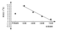
- FIG. 4 is a diagram showing the relationship between the yellowness of the Cu core ball 1 and the storage period.
- the vertical axis indicates yellowness
- the horizontal axis indicates the storage period.
- the contribution rate R 2 of the storage days and yellowness of the Cu nucleus ball 1 storage period at after 1 day 0.589, and the becomes a value away from the 1. Therefore, in the management based on yellowness, there is a problem that there are many variations in measured values, and the oxide film thickness cannot be managed with high accuracy.
- FIG. 4 is a graph showing the relationship between the oxide film thickness and the brightness of the Cu core ball 1.
- the vertical axis indicates the brightness
- the horizontal axis indicates the oxide film thickness.
- the oxide film thickness and brightness of the Cu core ball 1 have a correlation that the brightness decreases as the oxide film becomes thicker.
- Oxide film thickness and the contribution ratio R 2 of the brightness of Cu nuclei ball 1 0.9332, and becomes a value close to 1. Therefore, according to the management based on the brightness, there is little variation in the measured value, and the oxide film thickness can be managed with high accuracy.
- the measured value Prior to the baking test, the measured value has a large variation only by the management based on the brightness, and the oxide film thickness of the Cu core ball 1 cannot be managed with high accuracy.
- the reason why the oxide film thickness of the core ball 1 can be managed with high accuracy is considered as follows. In tests conducted before the firing test, details will be described later, but various conditions such as temperature, humidity, and heating time are changed, and various types of oxidation behavior are assumed.
- the object is to manufacture a Cu core ball that can suppress the formation of an oxide film thickness if it is mounted immediately after.
- the firing test of the present invention assumes Cu core balls that can suppress the growth of the oxide film thickness “after long-term storage”, and therefore it is necessary to assume various oxidation behaviors as in the test performed before the firing test.
- the fact that the growth behavior of the oxide film thickness is similar means that the change in brightness is also similar, and the correlation between the brightness and the oxide film thickness is improved. Therefore, in the present invention, the brightness is used as one index to accurately control the oxide film thickness of the Cu core ball 1 after the baking test.
- the Cu ball 2 constituting the Cu core ball 1 according to the present invention will be described in detail.
- bowl 2 since the structure of the Cu ball
- the Cu ball 2 does not melt at the soldering temperature when the Cu core ball 1 is used for a solder bump, and thus has a function of suppressing the height variation of the solder joint. Therefore, the Cu ball 2 preferably has a high sphericity and a small variation in diameter.
- the Cu ball 2 can be constituted by a composition of Cu alone or an alloy composition containing Cu as a main component. When the Cu ball 2 is made of an alloy, the Cu content is 50% by mass or more.
- Ni, Ag, Bi, Pb, Al, Sn, Fe, Zn, In, Ge, Sb, Co, Mn, Au, Si, Pt, Cr, La, Mo, Nb, Pd, Ti, Zr, and Mg may be composed of simple metals or alloys, metal oxides, or mixed metal oxides.
- the purity of the Cu ball 2 is not particularly limited, but is 99.9% or more from the viewpoint of suppressing deterioration of the electrical conductivity and thermal conductivity of the Cu ball 2 due to a decrease in purity, and suppressing the ⁇ dose as necessary. It is.
- the impurity element contained in the Cu ball 2 include Sn, Sb, Bi, Ni, Zn, Fe, Al, As, Ag, In, Cd, Pb, Au, P, S, and Co.
- the sphericity of the Cu ball 2 is 0.95 or more from the viewpoint of controlling the standoff height. If the sphericity of the Cu ball 2 is less than 0.95, the Cu ball 2 has an indefinite shape, so that bumps with non-uniform height are formed during bump formation, and the possibility of poor bonding is increased. Furthermore, when the Cu core ball 1 is mounted on the electrode and reflow is performed, the Cu core ball 1 is displaced and the self-alignment property is also deteriorated.
- the sphericity is more preferably 0.990 or more. In the present invention, the sphericity represents a deviation from the sphere.
- the sphericity is obtained by various methods such as a least square center method (LSC method), a minimum region center method (MZC method), a maximum inscribed center method (MIC method), and a minimum circumscribed center method (MCC method).
- LSC method least square center method
- MZC method minimum region center method
- MIC method maximum inscribed center method
- MCC method minimum circumscribed center method
- the sphericity is an arithmetic average value calculated when, for example, the diameter of each of the 500 Cu balls 2 is divided by the major axis, and the closer the value is to the upper limit of 1.00, the closer to the true sphere. Represents that.
- the length of the major axis and the length of the diameter mean a length measured by an ultra quick vision, ULTRA QV350-PRO measuring device manufactured by Mitutoyo Corporation.
- the diameter of the Cu ball 2 is 1 to 1000 ⁇ m. When the diameter of the Cu ball 2 is within this range, the spherical Cu ball 2 can be stably manufactured, and connection short-circuiting when the terminals are at a narrow pitch can be suppressed.
- the aggregate of “Cu core balls” can be called “Cu core powder”.
- the “Cu core powder” is an aggregate of a large number of Cu core balls 1 in which the individual Cu core balls 1 have the above-described characteristics. For example, it is distinguished from the single Cu core ball 1 in the form of use, such as being blended as a powder in a solder paste. Similarly, when used for forming solder bumps, the “Cu core powder” used in such a form is distinguished from a single Cu core ball 1 because it is normally handled as an aggregate.
- solder layer 3 constituting the Cu core ball 1 according to the present invention will be described in detail.
- the solder layer 3 melts due to the temperature during reflow, and functions as a bonding member that electrically bonds the electrode of the semiconductor package and the electrode of the printed circuit board.
- the solder layer 3 may have a composition of Sn alone, an alloy composition of a lead-free solder alloy containing Sn as a main component, or a composition of an Sn—Pb solder alloy.
- the Sn content is 40% by mass or more.
- the lead-free solder composition include, for example, Sn, Sn—Ag alloy, Sn—Cu alloy, Sn—Bi alloy, Sn—Ag—Cu alloy, Sn—In alloy, and predetermined alloy elements added thereto. Things. Examples of alloy elements to be added include Ag, Cu, In, Ni, Co, Sb, P, and Fe.
- the alloy composition of the solder layer 3 is preferably a Sn-3Ag-0.5Cu alloy from the viewpoint of thermal fatigue life.
- the thickness of the solder layer 3 is not particularly limited, but for example, 100 ⁇ m (one side) or less is sufficient. Generally, it may be 20 to 50 ⁇ m.
- Sn content of the lead-free solder alloy which has Sn as a main component in this invention Preferably Sn is 80% or more, More preferably, Sn is 90% or more.
- a layer made of one or more elements selected from Ni and Co covering the Cu ball 2, such as a Ni plating layer or a Co plating layer, may be provided between the surface of the Cu ball 2 and the solder layer 3. .
- the film thickness of the Ni plating layer, the Co plating layer, etc. is, for example, 0.1 to 20 ⁇ m on one side.
- the surface of the Cu core ball 1 may be coated with a flux.
- a heat-resistant plate such as a ceramic, which is provided with a plurality of circular grooves having a hemispherical shape at the bottom, is prepared.
- the diameter and depth of the groove are appropriately set according to the particle diameter of the Cu ball 2, and for example, the diameter is 0.8 mm and the depth is 0.88 mm.
- chip-shaped Cu materials hereinafter referred to as “chip materials” obtained by cutting the Cu thin wires as materials are put into the grooves of the heat-resistant plate one by one.
- the heat-resistant plate in which the chip material is put in the groove is heated to 1100 to 1300 ° C. in a furnace filled with a reducing gas, for example, ammonia decomposition gas, and heat-treated for 30 to 60 minutes.
- a reducing gas for example, ammonia decomposition gas
- the chip material melts and becomes spherical.
- bowl 2 is shape
- the formed Cu ball 2 is heat-treated again at 800 to 1000 ° C., which is a temperature lower than the melting point of Cu.
- molten Cu is dropped from an orifice provided at the bottom of the crucible, and this droplet is cooled to form a Cu ball 2, or a Cu cut metal is formed by thermal plasma with 1000 ⁇ m.
- a method of making a ball by heating to a temperature of °C or higher.
- the Cu balls 2 thus formed may be reheated at a temperature of 800 to 1000 ° C. for 30 to 60 minutes.
- the Cu material as the raw material of the Cu ball 2 may be heat-treated at 800 to 1000 ° C.
- the Cu material that is a raw material of the Cu ball 2 for example, pellets, wires, pillars, and the like can be used.
- the purity of the Cu material may be 99.9 to 99.99% from the viewpoint of preventing the purity of the Cu balls 2 from being lowered too much.
- the heat treatment described above may not be performed, and the molten Cu holding temperature may be lowered to about 1000 ° C. as in the prior art.
- the above-mentioned heat treatment may be omitted or changed as appropriate according to the purity of the Cu material.
- a known electrolytic plating method such as barrel plating, or a pump connected to a plating tank is used.
- a method of forming the solder layer 3 on the Cu ball 2 by turbulent flow of the plating solution is used.
- a Cu ball 2 having a diameter of 100 ⁇ m is coated with Ni plating having a film thickness (one side) of 2 ⁇ m, and then a Sn—Ag—Cu solder layer 3 having a film thickness (one side) of 18 ⁇ m is formed. Ball 1 is produced.
- the Sn—Ag—Cu-containing plating solution according to an embodiment of the present invention contains Sn, Ag, and Cu as essential components as a sulfonic acid and a metal component in a medium mainly composed of water.
- the plating solution is obtained by mixing a plating mother solution mainly composed of water and sulfonic acids and a metal compound, and preferably contains an organic complexing agent for the stability of metal ions.
- Examples of the metal compound in the plating solution include the following.
- Specific examples of the Sn compound include tin salts of organic sulfonic acids such as methanesulfonic acid, ethanesulfonic acid, 2-propanolsulfonic acid, p-phenolsulfonic acid, tin sulfate, tin oxide, tin nitrate, tin chloride, bromide.
- the 1st Sn compound of these is mentioned. These Sn compounds can be used individually by 1 type or in mixture of 2 or more types.
- examples include copper, copper gluconate, copper tartrate, copper lactate, copper succinate, copper sulfamate, copper borofluoride, copper silicofluoride and the like.
- These Cu compounds can be used individually by 1 type or in mixture of 2 or more types.
- Examples of the Ag compound include silver salts of the above organic sulfonic acids, silver sulfate, silver oxide, silver chloride, silver nitrate, silver bromide, silver iodide, silver phosphate, silver pyrophosphate, silver acetate, silver formate, silver citrate, Examples include silver gluconate, silver tartrate, silver lactate, silver succinate, silver sulfamate, silver borofluoride, and silver silicofluoride. These Ag compounds can be used individually by 1 type or in mixture of 2 or more types.
- the amount of each metal in the plating solution is 0.21 to 2 mol / L, preferably 0.25 to 1 mol / L as Sn 2+ , and 0.01 to 0.1 mol / L as Ag + , preferably 0.8. 02 to 0.05 mol / L, and Cu 2+ is 0.002 to 0.02 mol / L, preferably 0.003 to 0.01 mol / L.
- the amount of Sn 2+ may be adjusted in the present invention.
- the Ag ion concentration (Ag / Cu molar ratio) with respect to the Cu ion concentration is preferably in the range of 4.5 to 5.58. Within this range, the Sn—Ag—Cu solder layer 3 having a low melting point such as an Sn-3Ag—0.5Cu alloy can be formed.
- the deposition amount of a desired solder plating is estimated by the following formula (1) according to Faraday's law of electrolysis, the amount of electricity is calculated, and an electric current is passed through the plating solution so that the calculated amount of electricity is obtained. 2 and the plating process is performed while flowing the plating solution. The capacity of the plating tank can be determined according to the total amount of the Cu balls 2 and the plating solution.
- w (g) (I ⁇ t ⁇ M) / (Z ⁇ F) (1)
- w is the amount of electrolytic deposition (g)
- I is the current (A)
- t is the energization time (seconds)
- M is the atomic weight of the deposited element (118.71 in the case of Sn)
- Z is The valence (divalent in the case of Sn)
- F is the Faraday constant (96500 coulomb)
- Q (A ⁇ sec) is represented by (I ⁇ t).
- the Cu ball 2 and the plating solution are plated while flowing, but the method of flowing is not particularly limited.
- the Cu ball 2 and the plating solution can be caused to flow by rotation of the barrel as in the barrel electrolytic plating method.
- the Cu core ball 1 according to the present invention can be obtained by drying in the air or N 2 atmosphere.
- the cleaning liquid for example, pure water, an alcohol such as isopropyl alcohol, an organic solvent such as ketone (acetone), an acidic cleaning liquid such as trisodium phosphate, a basic cleaning liquid, or the like can be used.
- the cleaning liquid may be used alone or in combination with a plurality of cleaning liquids.
- cleaning methods for example, immersion cleaning, ultrasonic cleaning, spray cleaning, shower cleaning, jet cleaning, vacuum cleaning, degassing cleaning, barrel cleaning, rocking brush cleaning, jet bubbling cleaning, micro bubbling cleaning, etc. should be adopted. Can do. As the cleaning method, a single cleaning method may be employed or a plurality of cleaning methods may be combined depending on the required cleaning effect. Depending on the cleaning method, cleaning solution, and cleaning time, the plating residue remaining on the surface of the Cu core ball 1 after cleaning differs, and the oxidation level during storage also differs. It is possible to obtain a Cu core ball 1 that is difficult to perform.
- the nucleus which comprises Cu core ball 1 concerning the present invention can also be constituted by a resin ball.
- resin materials include amino resins, acrylic resins, ethylene-vinyl acetate resins, styrene-butadiene block copolymers, polyester resins, melamine resins, phenol resins, alkyd resins, polyimide resins, urethane resins, epoxy resins, and cross-linked resins.
- conductive plastics such as polyacetylene, polypyrrole, polythiophene, and polyaniline.
- the Cu core ball can be constituted by a resin ball and a Sn—Ag—Cu solder plating layer (coating layer) covering the surface of the resin ball.
- the kind of coating layer mentioned above and laminated structure are not limited to the said example.
- the oxidation level of the Cu core ball 1 is managed based on the brightness and the yellowness.
- the present invention is not limited to this.
- the oxidation level of the Cu core ball after cleaning may be controlled by directly managing the film thickness of the oxide film formed on the surface of the Cu core ball.
- Another Cu core ball according to the present invention includes a Cu ball that secures a gap between the semiconductor package and the printed circuit board, and a solder layer that covers the Cu ball, and is baked for 72 hours under an atmospheric humidity of 150 degrees.
- the oxide film thickness after the test is 4.9 nm or less.
- the oxide film thickness of the Cu core ball after the baking test is more preferably 3.1 nm or less.
- the oxide film thickness of the Cu core ball is more preferably 3.1 nm or less.
- solder material part 3
- the present invention can also be applied to the case where the shape of the solder material is a column type.
- the solder material has a column shape
- the solder material includes a column having a columnar shape and a solder layer covering the surface of the column.
- the solder material has a brightness 62.5 or higher at 0.99 ° C. 72 hours L * a * b * color system after baked test under atmospheric humidity, the solder material before tempering test L * a * b *
- the brightness in the color system is 65 or more, and the yellowness in the L * a * b * color system is 7.0 or less.
- Column materials include Cu, Ni, Ag, Bi, Pb, Al, Sn, Fe, Zn, In, Ge, Sb, Co, Mn, Au, Si, Pt, Cr, La, Mo, Nb, Pd, A single metal of Ti, Zr, or Mg, an alloy, a metal oxide, a mixed metal oxide, or a resin material can be used.
- the solder layer may have a composition of Sn alone, an alloy composition of a lead-free solder alloy containing Sn as a main component, or a composition of an Sn—Pb solder alloy. When the solder layer is made of an alloy, the Sn content is 40% by mass or more.
- Examples of the lead-free solder composition include, for example, Sn, Sn—Ag alloy, Sn—Cu alloy, Sn—Bi alloy, Sn—Ag—Cu alloy, Sn—In alloy, and predetermined alloy elements added thereto. Things. Examples of alloy elements to be added include Ag, Cu, In, Ni, Co, Sb, P, and Fe.
- the above-described Cu core ball 1 has substantially the same configuration function except for the shape (sphericity), and therefore the description is omitted for the sake of convenience.
- the Cu core ball 1 according to the present invention can be used for a solder joint of an electronic component.
- the solder joint refers to a structure in which, for example, a solder bump is mounted on an electrode of a printed board.
- the solder bump refers to a structure in which the Cu core ball 1 is mounted on an electrode of a semiconductor chip, for example.
- ⁇ Cu ball production A Cu wire having a purity of 99.995% or less was prepared. After putting each prepared in a crucible, the temperature of the crucible was raised to 1200 ° C. and a heat treatment was performed for 45 minutes. Subsequently, molten Cu droplets were dropped from an orifice provided at the bottom of the crucible, and the dropped droplets were cooled to form Cu balls having an average particle diameter of 100 ⁇ m.
- the sphericity of the produced Cu ball was measured using a CNC image measurement system. Specifically, an ultra quick vision, ULTRA QV350-PRO measuring device manufactured by Mitutoyo Corporation was used. In this example, the length of the major diameter of the Cu ball and the length of the diameter are measured by the measuring device, and the arithmetic average value of the value obtained by dividing the diameter of each of the 500 Cu balls by the major diameter is calculated to calculate the sphericity. Asked. The closer the value is to the upper limit of 1.00, the closer to a true sphere.
- a Ni plating layer having a film thickness (one side) of 2 ⁇ m is formed on the surface of the Cu ball having a diameter of 100 ⁇ m to prepare a Ni plating Cu ball having a diameter of 104 ⁇ m, and further a solder having a film thickness of 18 ⁇ m is formed on the surface of the Ni plating layer.
- a layer was formed to prepare a Cu core ball having a diameter of 140 ⁇ m.
- Sn-3Ag-0.5Cu alloy was used.
- the produced Cu core ball was put into a beaker containing pure water, and washed with stirring by a stirrer for 10 minutes.
- the oxide film thickness, brightness, and yellowness of the Cu core ball were measured under the conditions shown in the following examples and comparative examples.
- Example 1 Cu core balls immediately after cleaning were used.
- Example 2 Cu core balls that were stirred and washed were stored at room temperature (exposure to the atmosphere) and at a humidity of 30 to 40% for 2 days.
- Example 3 the Cu core balls that were stirred and washed were stored at room temperature and humidity of 30 to 40% for 5 days.
- Example 4 the Cu core ball that was stirred and washed was stored for 7 days at room temperature and humidity of 30 to 40%.
- Example 5 the Cu core ball that had been washed by stirring was stored at room temperature and humidity of 30 to 40% for 10 days.
- Example 6 the stirred and washed Cu core ball was stored for 14 days at room temperature and humidity of 30 to 40%.
- Example 7 the Cu core ball that was stirred and washed was stored at 40 ° C.
- Example 8 the stirred and washed Cu core ball was stored at room temperature and humidity of 30 to 40% for 20 days.
- stirred and washed Cu core balls were stored at 40 ° C. and 90% humidity for 2 days.
- the Cu core ball that was stirred and washed was stored at 200 ° C. for 1 hour. The room temperature is 20-30 ° C.
- Comparative Example 1 the stirred and washed Cu core ball was stored at 40 ° C. and 90% humidity for 5 days.
- the stirred and washed Cu core ball was stored for 7 days at 40 ° C. and 90% humidity.
- Comparative Example 3 the stirred and washed Cu core ball was stored at 40 ° C. and 90% humidity for 10 days.
- the Cu core ball that was stirred and washed was stored at 40 ° C. and a humidity of 90% for 14 days.
- Comparative Example 5 the stirred and washed Cu core ball was stored at 200 ° C. for 1 day.
- Comparative Example 6 the stirred and washed Cu core ball was stored at 200 ° C. for 2 days.
- the Cu core balls of Examples 1 to 10 and Comparative Examples 1 to 6 stored under the above conditions were recovered, and the brightness, yellowness, and oxide film thickness of each recovered Cu core ball were measured.
- the brightness and yellowness of the Cu core ball were measured using a CM-2600d spectrocolorimeter manufactured by Konica Minolta.
- the oxide film thickness of the Cu ball was measured using a FE-AES measuring device of ULVAC PHI700.
- the acceleration voltage of the measuring device was 10 kV, and the irradiation current was 10 nA.
- the oxide film thickness (depth) was determined from the speed (etching rate) of cutting the sample surface with ions (Ar), and the etching depth at which the half peak value of oxygen-derived intensity was used as the approximate oxide film thickness.
- the etching rate is a value converted to SiO 2 in terms of the cutting speed of the SiO 2 standard sample.
- Table 1 shows the relationship between the measured brightness and yellowness of Cu core balls and the oxide film thickness in each of Examples 1 to 10 and Comparative Examples 1 to 6. In Table 1, the unit of the oxide film thickness is (nm).
- the oxide film thickness is 3.8 nm. It became the following. Further, as shown in Examples 1 to 5 in Table 1, when a Cu core ball having a brightness of 70 or more and a yellowness of 5.1 or less is selected, the oxide film thickness is 1.9 nm. Thus, Cu core balls having a thinner oxide film thickness than those of other Examples 6 to 10 were obtained.
- the redness (a * value) was also measured, the correlation coefficient with the oxide film thickness and the contribution ratio were smaller than 1, and it was confirmed that the redness could not be used as an index for managing the oxide film thickness.
- the ⁇ dose of the Cu core balls of Examples 1 to 10 is 0.0010 cph / cm 2 or less, Lower than 0.0200 cph / cm 2 .
- Example 1A the Cu core ball that was stirred and cleaned was further cleaned by the first cleaning method, and then the cleaned Cu core ball was placed in the thermostat and stored at 150 ° C. for 3 days.
- Example 1B the Cu core ball that was stirred and cleaned was further cleaned by the second cleaning method, and then the cleaned Cu core ball was placed in the thermostat and stored at 150 ° C. for 3 days.
- Example 1C the Cu core ball that was stirred and cleaned was further cleaned by the third cleaning method, and then the cleaned Cu core ball was placed in the thermostat and stored at 150 ° C. for 3 days.
- Comparative Example 1A the above-described stirred and cleaned Cu core ball was placed in the thermostat and stored at 150 ° C. for 3 days.
- the prepared Cu core ball is put into a beaker containing pure water, the beaker containing the Cu core ball is set in an ultrasonic cleaner, and ultrasonic cleaning is performed for 10 seconds. It was.
- the prepared Cu core ball was put into a beaker containing pure water, the beaker containing the Cu core ball was set in an ultrasonic cleaner, and ultrasonic cleaning was performed for 60 seconds.
- the prepared Cu core ball was put into a beaker containing pure water, the beaker containing the Cu core ball was set in an ultrasonic cleaner, and ultrasonic cleaning was performed for 180 seconds.
- the first to third cleaning methods are classified into cleaning methods having a high cleaning effect that can sufficiently remove the plating solution residue. Moreover, the cleaning method only with stirring cleaning was classified as a cleaning method with a low cleaning effect in which the plating solution residue could not be sufficiently removed.
- each Cu core ball in Examples 1A, 1B, 1C and Comparative Example 1A cleaned and stored under the above conditions was recovered, and the brightness, yellowness, and oxide film thickness of each recovered Cu core ball were respectively determined. It was measured.
- the brightness and yellowness of the Cu core ball were measured using a CM-2600d spectrocolorimeter manufactured by Konica Minolta.
- the oxide film thickness of the Cu ball was measured using a FE-AES measuring device of ULVAC PHI700.
- the acceleration voltage of the measuring device was 10 kV, and the irradiation current was 10 nA.
- the oxide film thickness (depth) was determined from the speed (etching rate) of cutting the sample surface with ions (Ar), and the etching depth at which the half peak value of oxygen-derived intensity was used as the approximate oxide film thickness.
- the etching rate is a value converted to SiO 2 in terms of the cutting speed of the SiO 2 standard sample.
- Table 2 shows the relationship between the brightness, yellowness, and oxide film thickness of the Cu core balls measured in each of Examples 1A, 1B, 1C and Comparative Example 1A. In Table 2, the unit of the oxide film thickness is (nm).
- Comparative Example 1A of Table 2 when only stirring cleaning was performed as the cleaning condition, the brightness in the Cu core ball after the baking test was less than 62.5, and the oxide film thickness of the Cu core ball was It was over 4.9 nm. As a result, when a Cu core ball satisfying a condition that the lightness after heating and storage is less than 62.5 is selected, the cleaning is insufficient and the amount of solder plating solution residue increases. It has been found that Cu core balls are easily formed (thick oxide film).
- the example using the Cu core ball of Example 1 shown in Table 1 has been described, but the invention is not limited thereto. Even when the Cu core balls of Examples 2 to 10 shown in Table 1 were used, it was found that the same results as those obtained using the Cu core balls of Example 1 were obtained although not shown in the table. . Specifically, the brightness of the Cu core ball after the baking test was 62.5 or more, and the oxide film thickness of the Cu core ball was 4.9 nm or less.
- Table 3 shows the relationship between the brightness, yellowness and oxide film thickness of the Cu core ball immediately after the cleaning of the Cu core ball before heating and storage.
- the unit of the oxide film thickness is (nm).
- the brightness of the Cu core ball immediately after cleaning of the Cu core ball before the baking test was 71.2 or more, and the oxide film thickness was 1.2 nm or less. In this way, in the state immediately after cleaning and before performing the baking test, the growth of the oxide film due to the plating solution residue is not promoted, so even if the cleaning conditions are different, the oxide film thickness does not differ so much. Was confirmed.
- Table 4 shows the relationship between the brightness and yellowness of the Cu core ball and the oxide film thickness when a baking test is performed at a temperature of 150 ° C. for 5 days (120 hours).
- the unit of the oxide film thickness is (nm).
- Table 5 shows the relationship between the brightness and yellowness of the Cu core ball and the oxide film thickness when a baking test was performed at a temperature of 150 ° C. for 7 days (168 hours).
- the unit of the oxide film thickness is (nm).
Abstract
Description
図1は、本発明に係るCu核ボール1の構成の一例を示す断面図である。図1に示すように、本発明に係るCu核ボール1は、所定の大きさを有して半導体パッケージ(接合物)とプリント基板(被接合物)との間で間隔を確保するCuボール(核)2と、Cuボール2を被覆するはんだ層(被覆層)3とを備えている。
本発明に係るCu核ボール1は、焼き試験前のL*a*b*表色系における明度が65以上、かつ、L*a*b*表色系における黄色度が7.0以下である。明度および黄色度が上記範囲内のCu核ボール1を選定することにより、はんだ層3の表面に形成される酸化膜厚を一定値以下で管理することができる。
本発明に係るCu核ボール1は、焼き試験後のL*a*b*表色系における明度が62.5以上である。150℃の大気湿度下で72時間、Cu核ボール1を加熱する理由は、Cu核ボール1の洗浄後に残るめっき液残渣量に応じて形成される酸化膜を、長期間、例えば1か月間にわたる保管試験を行わなくても短時間で形成することができるからである。また、Cu核ボール1の明度が62.5以上とする理由は、焼き試験により酸化膜が所定の膜厚(4.9nm)を超えたCu核ボール1を正確に見分けて管理するためである。なお、Cu核ボール1のL*a*b*表色系における明度は、より好ましくは70.2以上である。この場合には、より酸化膜厚を厳しく管理できる。上述した2つの条件を満たすことで、Cu核ボール1の洗浄後におけるめっき液残渣量が少なく、長期保管後に酸化し難いCu核ボール1を簡易かつ容易に見分けることができる。
次に、本発明に係るCu核ボール1を構成するCuボール2について詳しく説明する。なお、Cuボール2の構成等は、焼き試験前後において共通しているため、以下にまとめて説明する。Cuボール2は、Cu核ボール1がはんだバンプに用いられる際、はんだ付けの温度で溶融しないため、はんだ継手の高さばらつきを抑制する機能を有する。したがって、Cuボール2は、真球度が高く直径のバラツキが少ない方が好ましい。
Cuボール2は、Cu単体の組成により構成することもできるし、Cuを主成分とする合金組成により構成することもできる。Cuボール2を合金により構成する場合、Cuの含有量は50質量%以上である。また、核となるボールとしては、Cu以外にも、Ni、Ag、Bi、Pb、Al、Sn、Fe、Zn、In、Ge、Sb、Co、Mn、Au、Si、Pt、Cr、La、Mo、Nb、Pd、Ti、Zr、Mgの金属単体や合金、金属酸化物、あるいは金属混合酸化物により構成しても良い。
Cuボール2の純度は特に限定されないが、純度の低下によるCuボール2の電気伝導度や熱伝導率の劣化を抑制し、また必要に応じてα線量を抑制する観点から、99.9%以上である。Cuボール2に含まれる不純物元素としては、Sn、Sb、Bi、Ni、Zn、Fe、Al、As、Ag、In、Cd、Pb、Au、P、S、Coなどが挙げられる。
Cuボール2の真球度は、スタンドオフ高さを制御する観点から0.95以上である。Cuボール2の真球度が0.95未満であると、Cuボール2が不定形状になるため、バンプ形成時に高さが不均一なバンプが形成され、接合不良が発生する可能性が高まる。さらに、Cu核ボール1を電極に搭載してリフローを行う際、Cu核ボール1が位置ずれを起こしてしまい、セルフアライメント性も悪化する。真球度は、より好ましくは0.990以上である。本発明において、真球度とは真球からのずれを表す。真球度は、例えば、最小二乗中心法(LSC法)、最小領域中心法(MZC法)、最大内接中心法(MIC法)、最小外接中心法(MCC法)など種々の方法で求められる。詳しくは、真球度とは、例えば500個の各Cuボール2の直径を長径で割った際に算出される算術平均値であり、値が上限である1.00に近いほど真球に近いことを表す。本発明での長径の長さ、および直径の長さとは、ミツトヨ社製のウルトラクイックビジョン、ULTRA QV350-PRO測定装置によって測定された長さをいう。
Cuボール2の直径は、1~1000μmである。Cuボール2の直径がこの範囲にあると、球状のCuボール2を安定して製造でき、また、端子間が狭ピッチである場合の接続短絡を抑制することができる。
次に、本発明に係るCu核ボール1を構成するはんだ層3について詳しく説明する。なお、はんだ層3の構成等は、焼き試験前後において共通しているため、以下にまとめて説明する。はんだ層3は、Cu核ボール1がはんだバンプに用いられる際、リフロー時の温度により溶融し、半導体パッケージの電極とプリント基板の電極とを電気的に接合する接合部材として機能する。
はんだ層3は、Sn単体の組成とすることもできるし、Snを主成分とする鉛フリーはんだ合金の合金組成とすることもできるし、Sn-Pbはんだ合金の組成とすることもできる。はんだ層3を合金により構成する場合、Snの含有量は40質量%以上である。鉛フリーはんだ組成の一例としては、例えば、Sn、Sn-Ag合金、Sn-Cu合金、Sn-Bi合金、Sn-Ag-Cu合金、Sn-In合金、およびこれらに所定の合金元素を添加したものが挙げられる。添加する合金元素としては、例えばAg、Cu、In、Ni、Co、Sb、P、Fe等が挙げられる。添加する合金元素の添加量については、鉛フリーはんだ合金の黄色度と明度がSn単体の黄色度と明度とほぼ同程度となる量に抑えるのが好ましい。これらの中でも、はんだ層3の合金組成は、熱疲労寿命の観点から、Sn-3Ag-0.5Cu合金が好ましい。はんだ層3の厚さは、特に制限されないが、例えば100μm(片側)以下であれば十分である。一般には20~50μmであれば良い。なお、本発明におけるSnを主成分とする鉛フリーはんだ合金のSnの含有量は、好ましくはSnが80%以上、より好ましくはSnが90%以上である。
次に、本発明に係るCu核ボール1の製造方法の一例を説明する。まず、セラミックのような耐熱性の板であって、底部に半球状をなす多数の円形の溝が設けられた耐熱板を用意する。溝の直径や深さは、Cuボール2の粒径に応じて適宜設定されており、例えば、直径が0.8mmであり、深さが0.88mmである。次に、材料となるCu細線を切断することで得られたチップ形状のCu材(以下、「チップ材」という。)を、耐熱板の溝内に一個ずつ投入する。
式(1)中、wは電解析出量(g)、Iは電流(A)、tは通電時間(秒)、Mは析出する元素の原子量(Snの場合、118.71)、Zは原子価(Snの場合は2価)、Fはファラデー定数(96500クーロン)であり、電気量Q(A・秒)は(I×t)で表される。
また、本発明に係るCu核ボール1を構成する核は、樹脂ボールにより構成することもできる。樹脂材料としては、例えばアミノ樹脂、アクリル樹脂、エチレン-酢酸ビニル樹脂、スチレン-ブタジエンブロック共重合体、ポリエステル樹脂、メラミン樹脂、フェノール樹脂、アルキド樹脂、ポリイミド樹脂、ウレタン樹脂、エポキシ樹脂、架橋樹脂等からなるものが挙げられる。中でもポリアセチレン、ポリピロール、ポリチオフェン、ポリアニリンなどの導電性プラスチック等を使用するのが好ましい。核を樹脂材料とした場合、樹脂ボールと、樹脂ボールの表面を被覆するSn-Ag-Cu系はんだめっき層(被覆層)によりCu核ボールを構成することができる。なお、上述した被覆層の種類や積層構造は、上記例に限定されるものではない。
上述した実施の形態では、明度と黄色度によりCu核ボール1の酸化レベルを管理した例について説明したが、これに限定されることはない。例えば、Cu核ボールの表面に形成される酸化膜の膜厚を直接管理することにより、洗浄後におけるCu核ボールの酸化レベルを管理しても良い。本発明に係る他のCu核ボールは、半導体パッケージとプリント基板との間で間隔を確保するCuボールと、Cuボールを被覆するはんだ層とを備え、150度の大気湿度下で72時間の焼き試験後の酸化膜厚が4.9nm以下である。焼き試験後におけるCu核ボールの酸化膜厚を4.9nm以下で管理することで、洗浄が十分に実施されており、酸化し難い(酸化膜の薄い)Cu核ボールを見分けて取得することができる。Cu核ボールの酸化膜厚は、より好ましくは3.1nm以下である。なお、上述したCu核ボール1と実質的に同一の構成機能については、便宜上説明を省略する。
上述した実施の形態では、はんだ材料の形状がボール型の場合について説明したが、はんだ材料の形状がカラム型の場合にも、本発明を適用することができる。はんだ材料をカラム形状とする場合、はんだ材料は、円柱状をなすカラムと、カラムの表面を被覆するはんだ層とから構成される。このはんだ材料は、150℃の大気湿度下で72時間の焼き試験後のL*a*b*表色系における明度が62.5以上であり、焼き試験前のはんだ材料のL*a*b*表色系における明度が65以上、かつ、L*a*b*表色系における黄色度が7.0以下である。
純度が99.995%以下のCuワイヤを準備した。準備した各々をるつぼの中に投入した後、るつぼの温度を1200℃に昇温し、45分間加熱処理を行った。続けて、るつぼ底部に設けたオリフィスから溶融Cuの液滴を滴下し、滴下した液滴を冷却して平均粒径が100μmのCuボールを造球した。
作製したCuボールの真球度は、CNC画像測定システムを使用して測定した。具体的には、ミツトヨ社製のウルトラクイックビジョン、ULTRA QV350-PRO測定装置を使用した。本実施例では、上記測定装置によりCuボールの長径の長さと直径の長さを測定し、500個の各Cuボールの直径を長径で割った値の算術平均値を算出して真球度を求めた。値が上限である1.00に近いほど真球に近いことを表す。
次に、作製した直径100μmのCuボールの表面に膜厚(片側)2μmのNiめっき層を形成して直径104μmのNiめっきCuボールを作製し、さらにNiめっき層の表面に膜厚18μmのはんだ層を形成して直径140μmのCu核ボールを作製した。はんだ層には、Sn-3Ag-0.5Cu合金を使用した。続けて、作製したCu核ボールを純水を入れたビーカーの中に投入し、攪拌機により10分間撹拌洗浄した。そして、Cu核ボールの酸化膜厚、明度および黄色度を、下記の各実施例および比較例に示す条件でそれぞれ測定した。

続けて、上述した実施例1の焼き試験前のCu核ボールを使用し、このCu核ボールに対して、短い期間にてCu核ボールを長期間保管した状態とするために焼き試験を実施した。続けて、焼き試験を行った後のCu核ボールの酸化膜厚、明度および黄色度をそれぞれ測定した。なお、使用するCu核ボールは、上述したように、10分間の撹拌洗浄が実施されている。
まず、温度25℃(室温)、湿度40%において、恒温槽を150℃に設定し、その状態を1時間以上維持した。実施例1Aでは、撹拌洗浄したCu核ボールをさらに第1の洗浄方法で洗浄した後、洗浄したCu核ボールを上記恒温槽に入れて150℃で3日間保管した。実施例1Bでは、撹拌洗浄したCu核ボールをさらに第2の洗浄方法で洗浄した後、洗浄したCu核ボールを上記恒温槽に入れて150℃で3日間保管した。実施例1Cでは、撹拌洗浄したCu核ボールをさらに第3の洗浄方法で洗浄した後、洗浄したCu核ボールを上記恒温槽に入れて150℃で3日間保管した。比較例1Aでは、上述した撹拌洗浄したCu核ボールを上記恒温槽に入れて150℃で3日間保管した。
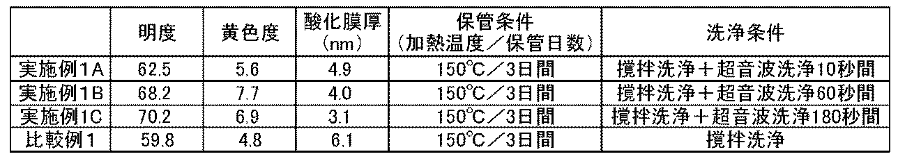
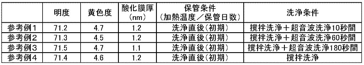


2 Cuボール(核)
3 はんだ層(被覆層)
Claims (13)
- 接合物と被接合物との間で間隔を確保する核と、
前記核を被覆するSnまたはSnを主成分とするはんだ合金から構成される被覆層とを備えたはんだ材料において、
温度が25℃、湿度が40%の室内における150℃の恒温槽での72時間の焼き試験後のL*a*b*表色系における明度が62.5以上であり、
前記焼き試験前の前記はんだ材料のL*a*b*表色系における明度が65以上、かつ、L*a*b*表色系における黄色度が7.0以下である
ことを特徴とするはんだ材料。 - Ni及びCoから選択される1元素以上からなる層で被覆された前記核が、前記はんだ層で被覆される
ことを特徴とする請求項1に記載のはんだ材料。 - 前記はんだ材料において、前記焼き試験後のL*a*b*表色系における前記明度が70.2以上である
ことを特徴とする請求項1または2に記載のはんだ材料。 - 前記核が球状のCu、Ni、Ag、Bi、Pb、Al、Sn、Fe、Zn、In、Ge、Sb、Co、Mn、Au、Si、Pt、Cr、La、Mo、Nb、Pd、Ti、Zr、Mgからなる群から選択される少なくとも1種類の元素、または樹脂材料によって構成されている
ことを特徴とする請求項1~3のいずれか1項に記載のはんだ材料。 - 前記核が円柱状のCu、Ni、Ag、Bi、Pb、Al、Sn、Fe、Zn、In、Ge、Sb、Co、Mn、Au、Si、Pt、Cr、La、Mo、Nb、Pd、Ti、Zr、Mgからなる群から選択される少なくとも1種類の元素、または樹脂材料によって構成されている
ことを特徴とする請求項1~3のいずれか1項に記載のはんだ材料。 - 請求項1~5のいずれか1項に記載のはんだ材料を使用したはんだ継手。
- 接合物と被接合物との間で間隔を確保する核と、
前記核を被覆するSnまたはSnを主成分とするはんだ合金から構成される被覆層とを備えたはんだ材料において、
温度が25℃、湿度が40%の室内における150℃の恒温槽での72時間の焼き試験後の酸化膜厚が4.9nm以下である
ことを特徴とするはんだ材料。 - Ni及びCoから選択される1元素以上からなる層で被覆された前記核が、前記はんだ層で被覆される
ことを特徴とする請求項7に記載のはんだ材料。 - 前記焼き試験後の前記酸化膜厚が3.1nm以下である
ことを特徴とする請求項7または8に記載のはんだ材料。 - 前記核が球状のCu、Ni、Ag、Bi、Pb、Al、Sn、Fe、Zn、In、Ge、Sb、Co、Mn、Au、Si、Pt、Cr、La、Mo、Nb、Pd、Ti、Zr、Mgからなる群から選択される少なくとも1種類の元素、または樹脂材料によって構成されている
ことを特徴とする請求項7~9のいずれか1項に記載のはんだ材料。 - 前記核が円柱状のCu、Ni、Ag、Bi、Pb、Al、Sn、Fe、Zn、In、Ge、Sb、Co、Mn、Au、Si、Pt、Cr、La、Mo、Nb、Pd、Ti、Zr、Mgからなる群から選択される少なくとも1種類の元素、または樹脂材料によって構成されている
ことを特徴とする請求項7~9のいずれか1項に記載のはんだ材料。 - 請求項7~11のいずれか1項に記載のはんだ材料を使用したはんだ継手。
- 接合物と被接合物との間で間隔を確保する核と、当該核を被覆するSnまたはSnを主成分とするはんだ合金から構成される被覆層とを備えたはんだ材料を、温度が25℃、湿度が40%の室内にて150℃に設定された恒温槽で72時間、加熱する工程と、
前記工程において加熱した前記はんだ材料のL*a*b*表色系における明度が62.5以上となるはんだ材料を取得する工程と、
を有することを特徴とするはんだ材料の検査方法。
Priority Applications (4)
| Application Number | Priority Date | Filing Date | Title |
|---|---|---|---|
| KR1020187002608A KR101867796B1 (ko) | 2015-06-29 | 2016-06-23 | 땜납 재료, 땜납 이음 및 땜납 재료의 검사 방법 |
| US15/740,484 US10888957B2 (en) | 2015-06-29 | 2016-06-23 | Soldering material |
| EP16817812.7A EP3315245A4 (en) | 2015-06-29 | 2016-06-23 | Soldering material, soldered joint, and method for inspecting soldering material |
| CN201680039077.7A CN107735212B (zh) | 2015-06-29 | 2016-06-23 | 软钎料材料、焊接接头和软钎料材料的检查方法 |
Applications Claiming Priority (2)
| Application Number | Priority Date | Filing Date | Title |
|---|---|---|---|
| JP2015129649A JP5850199B1 (ja) | 2015-06-29 | 2015-06-29 | はんだ材料、はんだ継手およびはんだ材料の検査方法 |
| JP2015-129649 | 2015-06-29 |
Publications (1)
| Publication Number | Publication Date |
|---|---|
| WO2017002704A1 true WO2017002704A1 (ja) | 2017-01-05 |
Family
ID=55237944
Family Applications (1)
| Application Number | Title | Priority Date | Filing Date |
|---|---|---|---|
| PCT/JP2016/068673 WO2017002704A1 (ja) | 2015-06-29 | 2016-06-23 | はんだ材料、はんだ継手およびはんだ材料の検査方法 |
Country Status (7)
| Country | Link |
|---|---|
| US (1) | US10888957B2 (ja) |
| EP (1) | EP3315245A4 (ja) |
| JP (1) | JP5850199B1 (ja) |
| KR (1) | KR101867796B1 (ja) |
| CN (1) | CN107735212B (ja) |
| TW (1) | TWI680194B (ja) |
| WO (1) | WO2017002704A1 (ja) |
Families Citing this family (13)
| Publication number | Priority date | Publication date | Assignee | Title |
|---|---|---|---|---|
| KR101904884B1 (ko) * | 2016-10-27 | 2018-10-10 | 덕산하이메탈(주) | 솔더볼 및 이를 이용한 반도체 패키지 |
| KR101904891B1 (ko) * | 2016-11-14 | 2018-10-10 | 덕산하이메탈(주) | 솔더볼 및 이를 이용한 임베디드 칩 패키지 |
| US10730150B2 (en) * | 2017-08-07 | 2020-08-04 | Honeywell International Inc. | Flowable brazing compositions and methods of brazing metal articles together using the same |
| CN107793758B (zh) * | 2017-11-15 | 2020-08-07 | 江苏亚宝绝缘材料股份有限公司 | 一种碳纳米管复合聚酰亚胺树脂的聚合物及其制备与应用 |
| JP6439893B1 (ja) * | 2018-05-25 | 2018-12-19 | 千住金属工業株式会社 | ハンダボール、ハンダ継手および接合方法 |
| JP6579253B1 (ja) * | 2018-11-09 | 2019-09-25 | 千住金属工業株式会社 | ハンダボール、ハンダ継手および接合方法 |
| US20220105583A1 (en) * | 2019-01-18 | 2022-04-07 | Mitsubishi Electric Corporation | Solder joint life predictor and solder joint life prediction method |
| CN110202295B (zh) * | 2019-05-24 | 2021-10-26 | 浙江强力控股有限公司 | 一种低温铝软钎焊锡膏及其制备方法 |
| JP7381267B2 (ja) * | 2019-09-18 | 2023-11-15 | ナブテスコ株式会社 | 金属付加製造用粉粒体、その製造方法、その選別装置、その選別方法、粉体の純度判定装置、粉体の純度判定方法、粉体の保管方法、粉体の保管容器、金属造形物の製造方法、および、金属造形物の製造装置 |
| CN111458328B (zh) * | 2020-04-26 | 2021-03-19 | 电子科技大学 | 一种检测印制电路板残留铜层分布的方法 |
| CN111560530A (zh) * | 2020-06-12 | 2020-08-21 | 无锡隆达金属材料有限公司 | 一种白铜合金熔液熔炼工艺 |
| CN111996413B (zh) * | 2020-08-21 | 2021-07-09 | 中国电子科技集团公司第三十八研究所 | 一种铅锡基焊料合金的制备方法及制得的焊料合金 |
| JP6892621B1 (ja) * | 2020-09-10 | 2021-06-23 | 千住金属工業株式会社 | 核材料、電子部品及びバンプ電極の形成方法 |
Citations (5)
| Publication number | Priority date | Publication date | Assignee | Title |
|---|---|---|---|---|
| WO2009090776A1 (ja) * | 2008-01-17 | 2009-07-23 | Horizon Technology Laboratory Co., Ltd. | 半導体装置およびその製造方法 |
| WO2012118202A1 (ja) * | 2011-03-02 | 2012-09-07 | セントラル硝子株式会社 | 導電部付きガラス板用端子構造体及びこれを用いたガラス板物品 |
| WO2014109052A1 (ja) * | 2013-01-11 | 2014-07-17 | 千住金属工業株式会社 | Cuボール |
| JP5585751B1 (ja) * | 2014-02-04 | 2014-09-10 | 千住金属工業株式会社 | Cuボール、Cu核ボール、はんだ継手、はんだペースト、およびフォームはんだ |
| JP5590259B1 (ja) * | 2014-01-28 | 2014-09-17 | 千住金属工業株式会社 | Cu核ボール、はんだペーストおよびはんだ継手 |
Family Cites Families (12)
| Publication number | Priority date | Publication date | Assignee | Title |
|---|---|---|---|---|
| WO1995024113A1 (fr) | 1994-03-01 | 1995-09-08 | Sumitomo Special Metals Company Limited | Boule en cuivre et procede de production de cette derniere |
| JP2007160401A (ja) | 2005-11-15 | 2007-06-28 | Hitachi Metals Ltd | はんだ合金、はんだボールおよびそれを用いたはんだ接合部 |
| JP5071802B2 (ja) * | 2008-04-08 | 2012-11-14 | 日立金属株式会社 | はんだボール、はんだ層及びはんだバンプ |
| JP5221231B2 (ja) * | 2008-07-18 | 2013-06-26 | 日立電線株式会社 | 太陽電池用リード線の製造方法 |
| CN106098829A (zh) | 2008-11-27 | 2016-11-09 | 日立金属株式会社 | 太阳能电池用导线和太阳能电池的制造方法 |
| JP5418894B2 (ja) * | 2009-07-24 | 2014-02-19 | 日立金属株式会社 | 電子部品用複合ボールの製造方法 |
| CN102166691A (zh) | 2010-02-25 | 2011-08-31 | 东莞市万丰纳米材料有限公司 | 一种微焊接材料 |
| JP5606994B2 (ja) | 2010-09-30 | 2014-10-15 | 株式会社神戸製鋼所 | 肉盛溶接材料及び肉盛溶接金属が溶接された機械部品 |
| CN103831543B (zh) | 2012-11-23 | 2016-08-24 | 吴永恒 | 无铅焊接材料及其制备方法 |
| JP5652560B1 (ja) | 2014-02-04 | 2015-01-14 | 千住金属工業株式会社 | Cu核ボール、はんだペースト、フォームはんだ及びはんだ継手 |
| WO2016071971A1 (ja) * | 2014-11-05 | 2016-05-12 | 千住金属工業株式会社 | はんだ材料、はんだペースト、フォームはんだ、はんだ継手、およびはんだ材料の管理方法 |
| JP6892568B2 (ja) * | 2015-12-21 | 2021-06-23 | ニホンハンダ株式会社 | 表面性に優れたSnを主成分とするはんだ合金の選別方法 |
-
2015
- 2015-06-29 JP JP2015129649A patent/JP5850199B1/ja active Active
-
2016
- 2016-06-23 EP EP16817812.7A patent/EP3315245A4/en not_active Withdrawn
- 2016-06-23 US US15/740,484 patent/US10888957B2/en active Active
- 2016-06-23 KR KR1020187002608A patent/KR101867796B1/ko active IP Right Grant
- 2016-06-23 WO PCT/JP2016/068673 patent/WO2017002704A1/ja active Application Filing
- 2016-06-23 CN CN201680039077.7A patent/CN107735212B/zh active Active
- 2016-06-28 TW TW105120278A patent/TWI680194B/zh active
Patent Citations (5)
| Publication number | Priority date | Publication date | Assignee | Title |
|---|---|---|---|---|
| WO2009090776A1 (ja) * | 2008-01-17 | 2009-07-23 | Horizon Technology Laboratory Co., Ltd. | 半導体装置およびその製造方法 |
| WO2012118202A1 (ja) * | 2011-03-02 | 2012-09-07 | セントラル硝子株式会社 | 導電部付きガラス板用端子構造体及びこれを用いたガラス板物品 |
| WO2014109052A1 (ja) * | 2013-01-11 | 2014-07-17 | 千住金属工業株式会社 | Cuボール |
| JP5590259B1 (ja) * | 2014-01-28 | 2014-09-17 | 千住金属工業株式会社 | Cu核ボール、はんだペーストおよびはんだ継手 |
| JP5585751B1 (ja) * | 2014-02-04 | 2014-09-10 | 千住金属工業株式会社 | Cuボール、Cu核ボール、はんだ継手、はんだペースト、およびフォームはんだ |
Non-Patent Citations (1)
| Title |
|---|
| See also references of EP3315245A4 * |
Also Published As
| Publication number | Publication date |
|---|---|
| EP3315245A4 (en) | 2018-11-21 |
| TW201715047A (zh) | 2017-05-01 |
| KR20180014217A (ko) | 2018-02-07 |
| CN107735212A (zh) | 2018-02-23 |
| KR101867796B1 (ko) | 2018-06-15 |
| TWI680194B (zh) | 2019-12-21 |
| CN107735212B (zh) | 2019-03-08 |
| JP5850199B1 (ja) | 2016-02-03 |
| US10888957B2 (en) | 2021-01-12 |
| EP3315245A1 (en) | 2018-05-02 |
| US20180281118A1 (en) | 2018-10-04 |
| JP2017013080A (ja) | 2017-01-19 |
Similar Documents
| Publication | Publication Date | Title |
|---|---|---|
| JP5850199B1 (ja) | はんだ材料、はんだ継手およびはんだ材料の検査方法 | |
| JP5846341B1 (ja) | はんだ材料、はんだペースト、フォームはんだ、はんだ継手、およびはんだ材料の管理方法 | |
| JP5408401B1 (ja) | Cu核ボール | |
| JP5590259B1 (ja) | Cu核ボール、はんだペーストおよびはんだ継手 | |
| JP5967316B2 (ja) | Cu核ボール、はんだペースト、フォームはんだ及びはんだ継手 | |
| JP6217836B1 (ja) | 核材料および半導体パッケージおよびバンプ電極の形成方法 | |
| JP6485580B1 (ja) | Cu核ボール、はんだ継手、はんだペースト及びフォームはんだ | |
| JP5652560B1 (ja) | Cu核ボール、はんだペースト、フォームはんだ及びはんだ継手 | |
| TWI761683B (zh) | Cu核球、焊接頭、焊膏及泡沫焊料 | |
| JP5510623B1 (ja) | Niボール、Ni核ボール、はんだ継手、フォームはんだ、はんだペースト | |
| JP5585750B1 (ja) | Cu核ボール、はんだ継手、フォームはんだ、およびはんだペースト | |
| JP6376266B1 (ja) | 核材料およびはんだ継手およびバンプ電極の形成方法 | |
| JP6572997B1 (ja) | Cu核ボール、はんだ継手、はんだペースト及びフォームはんだ | |
| JP6493604B1 (ja) | Cu核ボール、はんだ継手、はんだペースト及びフォームはんだ | |
| JP6572996B1 (ja) | Cu核ボール、はんだ継手、はんだペースト及びフォームはんだ | |
| JP6572998B1 (ja) | Cu核ボール、はんだ継手、はんだペースト及びフォームはんだ | |
| JP6485581B1 (ja) | Cu核ボール、はんだ継手、はんだペースト及びフォームはんだ |
Legal Events
| Date | Code | Title | Description |
|---|---|---|---|
| 121 | Ep: the epo has been informed by wipo that ep was designated in this application |
Ref document number: 16817812 Country of ref document: EP Kind code of ref document: A1 |
|
| NENP | Non-entry into the national phase |
Ref country code: DE |
|
| ENP | Entry into the national phase |
Ref document number: 20187002608 Country of ref document: KR Kind code of ref document: A |
|
| WWE | Wipo information: entry into national phase |
Ref document number: 2016817812 Country of ref document: EP |
|
| WWE | Wipo information: entry into national phase |
Ref document number: 15740484 Country of ref document: US |