WO2016203534A1 - 挿入部品位置決め検査方法及び挿入部品実装方法並びに挿入部品位置決め検査装置及び挿入部品実装装置 - Google Patents
挿入部品位置決め検査方法及び挿入部品実装方法並びに挿入部品位置決め検査装置及び挿入部品実装装置 Download PDFInfo
- Publication number
- WO2016203534A1 WO2016203534A1 PCT/JP2015/067241 JP2015067241W WO2016203534A1 WO 2016203534 A1 WO2016203534 A1 WO 2016203534A1 JP 2015067241 W JP2015067241 W JP 2015067241W WO 2016203534 A1 WO2016203534 A1 WO 2016203534A1
- Authority
- WO
- WIPO (PCT)
- Prior art keywords
- positioning
- component
- circuit board
- insertion component
- mounting
- Prior art date
Links
Images


Classifications
-
- H—ELECTRICITY
- H05—ELECTRIC TECHNIQUES NOT OTHERWISE PROVIDED FOR
- H05K—PRINTED CIRCUITS; CASINGS OR CONSTRUCTIONAL DETAILS OF ELECTRIC APPARATUS; MANUFACTURE OF ASSEMBLAGES OF ELECTRICAL COMPONENTS
- H05K13/00—Apparatus or processes specially adapted for manufacturing or adjusting assemblages of electric components
- H05K13/08—Monitoring manufacture of assemblages
- H05K13/081—Integration of optical monitoring devices in assembly lines; Processes using optical monitoring devices specially adapted for controlling devices or machines in assembly lines
- H05K13/0815—Controlling of component placement on the substrate during or after manufacturing
-
- H—ELECTRICITY
- H05—ELECTRIC TECHNIQUES NOT OTHERWISE PROVIDED FOR
- H05K—PRINTED CIRCUITS; CASINGS OR CONSTRUCTIONAL DETAILS OF ELECTRIC APPARATUS; MANUFACTURE OF ASSEMBLAGES OF ELECTRICAL COMPONENTS
- H05K13/00—Apparatus or processes specially adapted for manufacturing or adjusting assemblages of electric components
- H05K13/04—Mounting of components, e.g. of leadless components
- H05K13/0404—Pick-and-place heads or apparatus, e.g. with jaws
- H05K13/0413—Pick-and-place heads or apparatus, e.g. with jaws with orientation of the component while holding it; Drive mechanisms for gripping tools, e.g. lifting, lowering or turning of gripping tools
-
- H—ELECTRICITY
- H05—ELECTRIC TECHNIQUES NOT OTHERWISE PROVIDED FOR
- H05K—PRINTED CIRCUITS; CASINGS OR CONSTRUCTIONAL DETAILS OF ELECTRIC APPARATUS; MANUFACTURE OF ASSEMBLAGES OF ELECTRICAL COMPONENTS
- H05K13/00—Apparatus or processes specially adapted for manufacturing or adjusting assemblages of electric components
- H05K13/08—Monitoring manufacture of assemblages
- H05K13/081—Integration of optical monitoring devices in assembly lines; Processes using optical monitoring devices specially adapted for controlling devices or machines in assembly lines
- H05K13/0813—Controlling of single components prior to mounting, e.g. orientation, component geometry
Definitions
- the present invention provides a circuit in which an insertion part provided with a positioning projection and a surface mounting electrode is provided with a positioning hole for inserting the positioning projection and a land for connecting the surface mounting electrode.
- the present invention relates to an insertion component positioning inspection method, an insertion component mounting method, an insertion component positioning inspection device, and an insertion component mounting device that inspect whether or not they can be mounted on a substrate.
- Patent Document 1 Japanese Patent Laid-Open No. 9-35882
- Patent Document 2 Japanese Patent Laid-Open No. 8-69838
- the bonding strength of components such as connectors mounted on a circuit board is increased.
- a plurality of parts of the circuit board are provided with positioning protrusions projecting downward at a plurality of parts of the component, and the positioning protrusions are inserted into positioning holes formed in the plurality of parts of the circuit board.
- the component is positioned with reference to the positioning hole, and the surface mounting electrode portion (lead tip, bump, etc.) of the component is aligned with the land of the circuit board and reflow soldered. is there.
- a component provided with the positioning projection is referred to as an “insertion component”.
- the insertion component supplied by a component feeder such as a tray feeder is picked up by the mounting head of the component mounter and moved upwards of the circuit board. Then, the insertion component is imaged from the lower surface side by a component imaging camera, and the captured image is processed to recognize the position of the positioning projection of the insertion component, and based on the recognition result
- the insertion is performed based on the positioning holes at a plurality of positions on the circuit board.
- the method of confirming the position of the positioning hole of the circuit board is to image the reference mark of the circuit board clamped at the component mounting position in the component mounter with the mark imaging camera, and to detect the position of the reference mark of the circuit board.
- positioning is performed using the specification data (position data of positioning holes, lands, etc. based on the position of the reference mark) provided by the circuit board manufacturer based on the position of the reference mark. The position of the hole is judged.
- the positional relationship between the positioning projection of the insertion part and the surface mounting electrode part may vary due to manufacturing variations of the insertion part and deformation of the surface mounting electrode part such as leads.
- the position of the positioning projection on the circuit board is recognized, and the positioning projection on the insertion component is inserted into the positioning hole on the circuit board.
- the insertion part is positioned with reference to the positioning hole of the board, and the surface mounting electrode portion of the insertion part is aligned with the land of the circuit board.
- the surface mount electrode part may be displaced from the circuit board land due to deformation of the surface mount electrode part, etc., which causes poor connection between the surface mount electrode part of the insertion part and the circuit board land. Or reduced the connection reliability.
- the present invention connects an insertion part provided with a positioning projection and a surface mounting electrode, and connects the positioning hole into which the positioning projection is inserted and the surface mounting electrode.
- the positioning projection and the surface mounting electrode portion of the insertion component are separately provided.
- the captured image is processed to recognize the position of the positioning projection and the position of the surface mounting electrode, and the positioning projection of the insertion component Assuming that is inserted into the positioning hole of the circuit board, the amount of positional deviation between the surface mounting electrode portion of the insertion component and the land of the circuit board is calculated, and the positional deviation is calculated.
- the insertion part on whether is within the allowable range was made to check whether mountable on the circuit board.
- the amount of positional deviation between the surface mounting electrode portion and the land when the positioning projection of the insertion component is inserted into the positioning hole of the circuit board is within an allowable range. Only when the amount of positional deviation is within an allowable range, the insertion component can be mounted on the circuit board, and the surface mounting electrode portion of the insertion component and the circuit board can be mounted. Connection failure with the land can be prevented and connection reliability can be improved.
- the position hole position data and the land position data of the circuit board are the specification data (circuit board) provided by the circuit board manufacturer.
- Position data of positioning holes, lands and the like based on the position of the reference mark) may be used. In this case, it is only necessary to recognize an image of the position of the reference mark on the circuit board, and the image recognition of the position of the reference mark is performed to determine the component mounting position on the circuit board in the component mounting machine before component mounting. Therefore, it is sufficient to use the image recognition result as it is, and there is no need to newly add an image recognition process.
- the positioning hole and the land of the circuit board are imaged separately or simultaneously by the substrate imaging camera, and the captured image is processed to calculate the position displacement amount and the position of the positioning hole.
- the position of the land may be recognized. In this way, even if there are variations in the positions of the positioning holes and lands due to manufacturing variations in the circuit board, the variations in the positions of the positioning holes and lands can be image-recognized. It is possible to accurately inspect whether or not the positional deviation amount between the surface mounting electrode part and the land when the insertion part positioning protrusion is inserted into the positioning hole of the circuit board is within an allowable range. it can.
- the inner diameter of the positioning hole of the circuit board is slightly larger than the outer diameter of the positioning projection to facilitate the insertion of the positioning projection of the insertion component.
- a clearance (clearance) is formed between them, and the positioning projection can be shifted within the range of the clearance.
- the insertion component may be positioned so that the center of the positioning projection is aligned with the center of the positioning hole.
- an image including the positioning projections captured by the component imaging camera is processed to recognize the outer diameter of the positioning projections, and the positioning is captured by the board imaging camera.
- An image including the hole is processed to recognize the inner diameter of the positioning hole, and based on the recognition result, assuming that the positioning projection of the insertion part is inserted into the positioning hole of the circuit board, The positioning projection is shifted within the range to search for the minimum value of the positional deviation between the surface mounting electrode part of the inserted component and the land of the circuit board, and whether the minimum value of the positional deviation is within the allowable range. If it is determined whether or not the insertion component can be mounted on the circuit board, and if it is determined that mounting is possible, the position correction amount of the insertion component is determined so that the positional deviation amount is a minimum value. Also good.
- the positioning projection is shifted within the gap between the two, so that the surface mounting electrode portion of the inserted component and the circuit board land
- the positioning projection is shifted within the gap between the two, so that the surface mounting electrode portion of the inserted component and the circuit board land
- the surface mounting is performed when mounting the insertion component on the circuit board in order to obtain the position correction amount of the insertion component that minimizes the amount of displacement between the surface mounting electrode section and the land.
- the inserted component can be mounted on the circuit board so that the amount of positional deviation between the electrode portion for use and the land is minimized, and the connection reliability between the surface mount electrode portion and the land can be improved.
- the above-described insertion component positioning inspection method is used to inspect whether the insertion component can be mounted on the circuit board.
- the determined insertion component may be discarded at a predetermined disposal location or collection location, and only the insertion component determined to be mountable may be mounted on the circuit board.
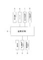
- FIG. 1 is a perspective view showing a configuration of a module type component mounting system in Embodiment 1 of the present invention.
- FIG. 2 is a perspective view showing a positional relationship among a mounting head, a component imaging camera, a coaxial incident illumination light source, and a side illumination laser light source.
- FIG. 3 is a block diagram showing the configuration of the control system of the component mounter.
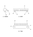
- 4A is a front view of the insertion part
- FIG. 4B is a bottom view of the insertion part
- FIG. 4C is a left side view of the insertion part.
- FIG. 5 is a diagram illustrating a configuration example of a circuit board on which an insertion component is mounted.
- FIG. 5 is a diagram illustrating a configuration example of a circuit board on which an insertion component is mounted.
- FIG. 6 is a plan view showing a mounting example when the amount of positional deviation between the surface mounting electrode portion of the insertion component and the land of the circuit board is within an allowable range.
- FIG. 7 is a plan view showing an example in which the amount of positional deviation between the surface mounting electrode portion of the insertion component and the land of the circuit board exceeds the allowable range, resulting in mounting failure.
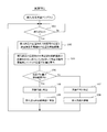
- FIG. 8 is a flowchart illustrating a flow of processing of the insertion component mounting program according to the first embodiment.
- FIG. 9 is a flowchart illustrating a flow of processing of the insertion component mounting program according to the third embodiment.
- FIGS. 1 to 3 A first embodiment in which the present invention is applied to a modular component mounting system will be described with reference to FIGS. First, the configuration of the modular component mounting system will be described with reference to FIGS. 1 to 3.
- Each component mounting machine 12 includes a component feeder 14 such as a tape feeder and a tray feeder, a conveyor 15 that conveys a circuit board 43 (see FIGS. 5 to 7), and one or a plurality of ones on a main body bed 13.
- a mounting head 17 that holds the suction nozzle 21 (see FIG.
- a head moving device 22 that moves the mounting head 17 in the X and Y directions, and a suction nozzle 21 of the mounting head 17 or
- a component imaging camera 16 or the like that images components (such as an insertion component 41 described later) held by the chuck from the lower surface side is mounted, and a display device such as a liquid crystal display or CRT is provided on the front surface of the upper frame 18.
- 19 and an operation unit 20 such as an operation key and a touch panel are provided.
- a substrate imaging camera 23 (see FIG. 3) for imaging a reference mark (not shown) on the circuit board 43 is attached to the head moving device 22 so as to move integrally with the mounting head 17 in the XY directions. ing.
- the circuit board 43 shown in FIGS. 5 to 7 shows only the portion on which the insertion component 41 is mounted, and the portion on which other electronic components are mounted is not shown.
- the mounting head 17 is rotatably assembled to a support bracket 24 that moves in the XY directions by a head moving device 22, and a suction nozzle moves around the central axis of the mounting head 17 by a head rotating motor 25.
- the suction nozzle 21 is configured to rotate intermittently (pitch drive) by 21 arrangement pitch angles, and to rotate the suction nozzle 21 integrally with the rotation of the mounting head 17.
- a plurality of nozzle holders 26 that hold the suction nozzle 21 are assembled to the mounting head 17 so as to be movable up and down (Z direction), and the mounting head 17 rotates at a predetermined rotation during a component suction operation or a component mounting operation.
- One nozzle holder 26 (suction nozzle 21) located at a position is moved up and down by a nozzle lifting mechanism 28 using a nozzle lifting motor 27 as a drive source.
- the suction nozzle 21 of each nozzle holder 26 is configured to be rotated (spinned) by a nozzle rotation motor 29, and the inclination (shift in the horizontal rotation angle) of the component sucked by each suction nozzle 21 is determined as component mounting. Correction is made by rotation of each suction nozzle 21 before.
- the component imaging camera 16 is arranged upward near the component suction position of the component supply device 14.
- a coaxial epi-illumination light source 32 is mounted upward via a lens 31 above the component imaging camera 16.
- the coaxial epi-illumination light source 32 is configured by arranging light emitting elements such as LEDs in an annular shape coaxial with the optical axis of the component imaging camera 16, and the component held on the suction nozzle 21 or the chuck at the time of component imaging is on its lower surface side. It comes to illuminate from.
- On the upper surface side of the frame-shaped illumination cover 33 of the coaxial epi-illumination light source 32 four laser light sources 34 that emit laser light in the horizontal direction toward the optical axis of the component imaging camera 16 are assembled at 90 ° intervals. ing.
- an illumination light source for imaging the positioning projection 42 of the insertion component 41 from below by the component imaging camera 16 The four laser light sources 34 are used, and the insertion component 41 held by the suction nozzle 21 or the chuck is lowered until the height position of the positioning projection 42 is the same height position as the optical axis of the laser light source 34. Then, the laser light emitted in the horizontal direction from the four laser light sources 34 is irradiated to the outer peripheral surface of the positioning projection 42 of the insertion component 41, and an image including the positioning projection 42 is captured by the component imaging camera 16.
- the shape of the lower end surface of the positioning projection 42 is distinguished from the lower surface of the insertion component 41 and can be clearly recognized from the image.
- the positioning projection is formed from an image obtained by illuminating the lower surface side of the insertion component 41 with the coaxial incident illumination light source 32 such that the lower end surface of the positioning projection 42 is colored differently from the lower surface of the insertion component 41. If the shape of the lower end surface of the part 42 can be recognized separately from the lower surface of the insertion part 41, the lower surface side of the insertion part 41 is illuminated by the coaxial incident illumination light source 32 and an image including the positioning protrusion 42 is captured. Then, the position of the positioning projection 42 may be recognized from the image.
- Each component mounter 12 transports the circuit board 43 conveyed from the upstream component mounter 12 to a predetermined position by the conveyor 15, and clamps and positions the circuit board 43 by a clamp mechanism (not shown). Thereafter, the reference mark on the circuit board 43 is imaged by the board imaging camera 23, the captured image is processed to recognize the position of the reference mark on the circuit board 43, and the component supplied by the component supply device 14. Is held by the suction nozzle 21 or the chuck of the mounting head 17, the part is moved to the imaging position, the image is picked up by the part imaging camera 16, and the conveyor 15 Mount on the upper circuit board 43.
- the specification data provided by the manufacturer of the circuit board 43 (data on the component mounting position of the circuit board 43 based on the position of the reference mark) is used.
- the component mounting position of the circuit board 43 is determined, and the positional deviation and inclination (horizontal rotation angle deviation) of the component held by the suction nozzle 21 or the chuck of the mounting head 17 are corrected to place the component on the circuit board 43. Mount at the component mounting position.
- the insertion component 41 is a large component such as a connector component, for example.
- a plurality of insertion components 41 are provided on the lower surface of the insertion component 41.
- Positioning projections 42 (for example, bosses, pins, etc.) projecting downward are provided at locations (for example, two locations), and the positioning projections 42 are formed in positioning holes 44 formed at a plurality of locations (for example, two locations) of the circuit board 43.
- the insertion component 41 when the insertion component 41 is mounted on the circuit board 43 by the component mounter 12, the insertion component 41 supplied by the component feeder 14 such as a tray feeder is picked up by the mounting head 17 of the component mounter 12, and the circuit is mounted. While moving the board 43 upward, the insertion component 41 is imaged from the lower surface side by the component imaging camera 16 and the captured image is processed, whereby the position of the positioning projection 42 of the insertion component 41 is determined. , And the positional deviation and inclination (horizontal rotation angle deviation) of the insertion part 41 are corrected based on the recognition result, and the positioning projection 42 of the insertion part 41 is positioned on the circuit board 43.
- the insertion component 41 By inserting into the hole 44, the insertion component 41 is positioned with reference to the positioning holes 44 at a plurality of locations of the circuit board 43, and the surface arranged in line with the insertion component 41 (Tip of the example lead, bump, etc.) wearing electrode portion 45 so as to reflow soldering by aligning the land 46 of the circuit board 43.
- the insertion component 41 may be positioned with reference to the positioning hole 44 of the circuit board 43 and the surface mounting electrode portion 45 of the insertion component 41 is aligned with the land 46 of the circuit board 43, the insertion component 41
- the surface mounting electrode portion 45 may be displaced from the land 46 of the circuit board 43 due to manufacturing variations of the surface mounting and deformation of the surface mounting electrode portion 45, and this may cause the surface mounting electrode portion 45 of the insertion component 41 and the circuit board 43 to be displaced. This may cause a connection failure with the land 46 or reduce connection reliability.
- the control device 51 that controls the operation of each mechanism of the component mounting machine 12 also functions as an insertion component positioning inspection device by executing the insertion component mounting program of FIG.
- the component picked up at 17 is the insertion component 41
- the positioning projection 42 and the surface mounting electrode portion 45 of the insertion component 41 are imaged separately or simultaneously by the component imaging camera 16, and the captured image
- it functions as an image processing means for recognizing the position of the positioning projection 42 and the position of the surface mounting electrode 45, and the positioning projection 42 of the insertion component 41 is positioned in the positioning hole 44 of the circuit board 43.
- misregistration amount calculating means for calculating the misregistration amount between the surface mounting electrode portion 45 of the insertion component 41 and the land 46 of the circuit board 43. And ability, further, the calculated position shift amount is inserted part 41 whether it is within the allowable range also functions as a check means for checking whether mountable on a circuit board 43. Further, when the control device 51 of the component mounting machine 12 determines that the positional displacement amount between the surface mounting electrode portion 45 of the insertion component 41 and the land 46 of the circuit board 43 exceeds the allowable range and mounting is impossible, the insertion is performed. Control is performed so that the component 41 is discarded at a predetermined disposal location or collection location, and only the insertion component 41 determined to be mountable is mounted on the circuit board 43.
- step 101 it is determined whether or not the component picked up by the suction nozzle 21 or the chuck of the mounting head 17 is the insertion component 41, and the insertion component. If not 41, it waits until the insertion part 41 is picked up.
- step 102 the mounting head 17 is moved above the component imaging camera 16 by the head moving device 22, and the insertion component 41 is moved.
- the four laser light sources 34 are used as illumination light sources when the component projection camera 42 is imaged from below with the component imaging camera 16, and the insertion component 41 held by the suction nozzle 21 or the chuck is placed on the positioning projection 42.
- the component imaging camera 16 captures an image including the positioning protrusion 42, and the image is processed to determine the positioning protrusion. It recognizes the position of 42. Further, the coaxial epi-illumination light source 3 is used as an illumination light source when the surface-mounting electrode portion 45 of the insertion component 41 is imaged by the component imaging camera 16 from below, and the lower surface side of the insertion component 41 is disposed on the coaxial epi-illumination light source 32. The component imaging camera 16 captures an image including the surface mounting electrode unit 45, and the image is processed to recognize the position of the surface mounting electrode unit 45.
- the positioning projection is formed from an image obtained by illuminating the lower surface side of the insertion component 41 with the coaxial incident illumination light source 32 such that the lower end surface of the positioning projection 42 is colored differently from the lower surface of the insertion component 41.
- the shape of the lower end surface of the portion 42 can be recognized separately from the lower surface of the insertion component 41, the lower surface side of the insertion component 41 is illuminated by the coaxial incident illumination light source 32, and the positioning projection 42 and the surface mounting electrode An image including both of the portions 45 may be taken, and the positions of both the positioning projections 42 and the surface mounting electrode portions 45 may be recognized from the images.
- the reference mark of the circuit board 43 is imaged by the board imaging camera 23 and the captured image is obtained. To recognize the position of the reference mark on the circuit board 43. Since the image recognition of the position of the reference mark is performed to determine the component mounting position of the circuit board 43 in the component mounter 12 before component mounting, the image recognition result may be used as it is, and a new image recognition is performed. There is no need to add processing.
- step 103 After recognizing the position of the positioning projection 42 and the position of the surface mounting electrode unit 45 in step 102, the process proceeds to step 103, and the recognition result of the position of the positioning projection 42 and the position of the surface mounting electrode unit 45 is obtained. Based on the above, it is assumed that the positioning projection 42 of the insertion component 41 is inserted into the positioning hole 44 of the circuit board 43, and the positional deviation between the surface mounting electrode portion 45 of the insertion component 41 and the land 46 of the circuit board 43. Calculate the amount. At this time, the insertion component 41 is positioned so that the center of the positioning protrusion 42 is aligned with the center of the positioning hole 44.
- the data of the position of the positioning hole 44 of the circuit board 43 and the position of the land 46 are the positions of the reference marks of the circuit board 43 recognized from the image obtained by previously imaging the reference marks of the circuit board 43 by the board imaging camera 23. Based on the specification data provided by the manufacturer of the circuit board 43 (data on the position of the positioning hole 44 and the position of the land 46 on the basis of the position of the reference mark).
- step 104 it is determined whether or not the positional deviation amount calculated in step 103 is within an allowable range. As a result, if it is determined that the positional deviation amount is within the allowable range, step 105 is performed. Then, it is determined that the insertion part 41 can be mounted on the circuit board 43. In the next step 106, the insertion part 41 is mounted on the circuit board 43, and the process returns to step 101 to repeat the above-described processing.
- step 104 determines whether the amount of displacement calculated in step 103 exceeds the allowable range. If it is determined in step 104 that the amount of displacement calculated in step 103 exceeds the allowable range, the process proceeds to step 107, where it is determined that mounting is not possible. 41 is discarded at a predetermined disposal place or collection place, the process returns to the step 101 and the above-described processing is repeated.
- the positioning projection 42 and the surface mounting electrode portion 45 of the insertion component 41 are imaged separately or simultaneously by the component imaging camera 16, and the position of the positioning projection 42 is detected. Assuming that the position of the surface mounting electrode portion 45 is recognized and the positioning projection 42 of the insertion component 41 is inserted into the positioning hole 44 of the circuit board 43, the surface mounting electrode portion 45 of the insertion component 41 and the circuit Since the amount of displacement of the substrate 43 from the land 46 is calculated and whether or not the insertion component 41 can be mounted on the circuit board 43 is determined based on whether or not the amount of displacement is within an allowable range.
- the positional deviation amount between the surface mounting electrode portion 45 and the land 46 when the positioning projection 42 of the insertion component 41 is inserted into the positioning hole 44 of the circuit board 43 is reduced.
- the insertion component 41 can be mounted on the circuit board 43 only when the amount of positional deviation is within an allowable range.
- the surface mounting electrode portion 45 of the insertion component 41 and the circuit can be mounted. Connection failure of the substrate 43 with the land 46 can be prevented in advance, and connection reliability can be improved.
- Example 2 of the present invention will be described.
- substantially the same parts as those in the first embodiment are denoted by the same reference numerals, description thereof is omitted or simplified, and different parts are mainly described.
- the data of the position of the positioning hole 44 and the position of the land 46 of the circuit board 43 is based on the position of the reference mark of the circuit board 43 recognized from the image captured by the board imaging camera 23 in advance.
- the data is obtained from the specification data provided by the manufacturer of the circuit board 43 (data on the position of the positioning hole 44 and the position of the land 46 on the basis of the position of the reference mark).
- the positioning holes 44 and the lands 46 of the circuit board 43 are imaged separately or simultaneously by the substrate imaging camera 23, and the captured images are processed, whereby the positional deviation between the surface mounting electrode unit 45 and the lands 46 is achieved.
- the position of the positioning hole 44 and the position of the land 46 of the circuit board 43 used when calculating the quantity are recognized.
- the variations in the positions of the positioning holes 44 and lands 46 can be recognized, so that the positioning holes 44 and the lands 46 can be recognized.
- the positional deviation amount between the surface mounting electrode portion 45 and the land 46 when the positioning projection 42 of the insertion component 41 is inserted into the positioning hole 44 of the circuit board 43 is allowed. It is possible to accurately inspect whether it is within the range.
- Embodiment 3 of the present invention will be described with reference to FIG.
- substantially the same parts as those in the first and second embodiments are denoted by the same reference numerals, description thereof is omitted or simplified, and different parts are mainly described.
- the inner diameter of the positioning hole 44 of the circuit board 41 is formed to be slightly larger than the outer diameter of the positioning projection 42 in order to facilitate the insertion of the positioning projection 42 of the insertion component 41. Therefore, when the positioning projection 42 of the insertion component 41 is inserted into the positioning hole 44 of the circuit board 43, a clearance (clearance) is formed between them, and the positioning projection 42 can be shifted within the range of the clearance. it can. When ignoring the effect of this gap, the insertion component 41 may be positioned so that the center of the positioning projection 42 coincides with the center of the positioning hole 44 as in the first embodiment.
- the control device 51 of the component mounting machine 12 executes the insertion component mounting program shown in FIG.
- the image including the portion 42 is processed to recognize the outer diameter of the positioning projection 42, and the image including the positioning hole 44 imaged by the board imaging camera 23 is processed by another program to obtain the inner diameter of the positioning hole 44.
- the positioning projections 42 of the insertion component 41 are inserted into the positioning holes 44 of the circuit board 43 based on the recognition results, the positioning projections 42 are moved within the gap between the two.
- the minimum value of the positional deviation amount between the surface mounting electrode portion 45 of the insertion component 41 and the land 46 of the circuit board 43 is searched for, and the insertion is performed depending on whether or not the minimum value of the positional deviation amount is within an allowable range. Part If it is determined whether or not 41 can be mounted on the circuit board 43 and it is determined that mounting is possible, the position correction amount of the insertion component 41 at which the positional deviation amount becomes the minimum value is obtained, and the position correction amount is determined according to the position correction amount. The mounting position of the insertion component 41 is corrected and mounted on the circuit board 43.
- step 201 it is determined whether or not the component picked up by the suction nozzle 21 or the chuck of the mounting head 17 is the insertion component 41, and the insertion component. If not 41, it waits until the insertion part 41 is picked up.
- step 202 where the mounting head 17 is moved above the component imaging camera 16 by the head moving device 22, and the insertion component 41 is moved.
- the four laser light sources 34 are used as illumination light sources when the component projection camera 42 is imaged from below with the component imaging camera 16, and the insertion component 41 held by the suction nozzle 21 or the chuck is placed on the positioning projection 42.
- the part imaging camera 16 captures an image including the positioning projection 42 and the position and position of the positioning projection 42. Recognize. Further, the lower surface side of the insertion component 41 is illuminated by the coaxial incident illumination light source 32, and an image including the surface mounting electrode unit 45 is captured by the component imaging camera 16 to recognize the position of the surface mounting electrode unit 45.
- the reference mark of the circuit board 43 is imaged by the board imaging camera 23 and the circuit board 43 is captured.
- the substrate imaging camera 23 captures an image including the positioning hole 44 to recognize the inner diameter of the positioning hole 44.
- the reference mark and the positioning hole 44 of the circuit board 43 may be imaged simultaneously by the board imaging camera 23 or may be separately imaged.
- the data of the position of the land 46 of the circuit board 43 may be obtained from the specification data provided from the manufacturer of the circuit board 43 as in the first embodiment, or the board imaging as in the second embodiment.
- the camera 23 may pick up an image and recognize it.
- step 203 After recognizing the position and outer diameter of the positioning protrusion 42 and the position of the surface mounting electrode section 45 in step 202, the process proceeds to step 203, where the position and outer diameter of the positioning protrusion 42 and the surface mounting electrode section are moved. Assuming that the positioning projection 42 of the insertion component 41 is inserted into the positioning hole 44 of the circuit board 43 based on the recognition result of the position 45, the positioning projection 42 is shifted within the gap between the two. The minimum value of the positional deviation amount between the surface mounting electrode portion 45 of the insertion component 41 and the land 46 of the circuit board 43 is searched.
- step 204 it is determined whether or not the searched minimum value of the positional deviation amount is within the allowable range. As a result, if it is determined that the minimum value of the positional deviation amount is within the allowable range, Proceeding to 205, it is determined that the insertion component 41 can be mounted on the circuit board 43. In this case, in the next step 206, after obtaining the position correction amount of the insertion part 41 at which the positional deviation amount becomes the minimum value, the process proceeds to step 207, where the insertion part 41 is mounted according to the position correction amount of the insertion part 41. The position is corrected and mounted on the circuit board 43, the process returns to step 201, and the above-described processing is repeated.
- step 204 determines whether the searched minimum value of the positional deviation amount exceeds the allowable range. If it is determined in step 204 that the searched minimum value of the positional deviation amount exceeds the allowable range, the process proceeds to step 208, where it is determined that mounting is impossible, and in the next step 209, the inserted component 41 is determined. Is discarded at a predetermined disposal place or collection place, the process returns to step 201 and the above-described processing is repeated.
- the positioning projection 42 of the insertion component 41 is inserted into the positioning hole 44 of the circuit board 43, the positioning projection 42 is placed within the gap between the two.
- the minimum value of the positional deviation amount between the surface mounting electrode portion 45 of the insertion component 41 and the land 46 of the circuit board 43 is searched for, and the insertion is performed depending on whether or not the minimum value of the positional deviation amount is within an allowable range.
- the gap between the positioning projection 42 and the positioning hole 44 is used effectively, and the surface mounting electrode portion 45 of the insertion component 41 and Inspecting whether or not the insertion component 41 can be mounted on the circuit board 43 by minimizing the amount of positional deviation of the circuit board 43 from the land 46 and determining whether the minimum value of the positional deviation is within an allowable range.
- the positioning projection 42 and Accurate inspection is possible in consideration of the gap between the-decided Me holes 44.
- the insertion component 41 is mounted on the circuit board 43 in order to obtain the position correction amount of the insertion component 41 at which the positional deviation amount between the surface mounting electrode portion 45 and the land 46 is minimized.
- the insertion component 41 can be mounted on the circuit board 43 so that the positional deviation between the surface mounting electrode section 45 and the land 46 is minimized, and the connection reliability between the surface mounting electrode section 45 and the land 46 is reliable. Can be improved.
- the present invention is not limited to the first to third embodiments.
- the configuration of the component mounting machine 12 may be changed as appropriate, or the configuration of the insertion component 41 and the circuit board 43 may be changed as appropriate. It goes without saying that various modifications can be made without departing from the scope.
- SYMBOLS 12 ... Component mounting machine, 14 ... Component supply apparatus, 15 ... Conveyor, 16 ... Component imaging camera, 17 ... Mounting head, 21 ... Adsorption nozzle, 22 ... Head moving device, 23 ... Board imaging camera, 32 ... Coaxial incident light Illumination light source 34 ... laser light source 41 ... insertion part 42 ... positioning projection 43 ... circuit board 44 ... positioning hole 45 ... surface mounting electrode part 46 ... land 51 ... control device (image processing means) , Position deviation calculation means, inspection means)
Abstract
Description
まず、図1乃至図3を用いてモジュール型部品実装システムの構成を説明する。
Claims (8)
- 位置決め用突起部と表面実装用電極部とが設けられた挿入部品を、前記位置決め用突起部を挿入する位置決め孔と前記表面実装用電極部を接続するランドとが設けられた回路基板に実装可能か否かを検査する挿入部品位置決め検査方法において、
前記挿入部品の前記位置決め用突起部と前記表面実装用電極部とを別々に又は同時に部品撮像用カメラで撮像して、その撮像画像を処理することで、前記位置決め用突起部の位置と前記表面実装用電極部の位置を認識し、
前記挿入部品の前記位置決め用突起部を前記回路基板の前記位置決め孔に挿入したと仮定して、前記挿入部品の前記表面実装用電極部と前記回路基板の前記ランドとの位置ずれ量を算出し、その位置ずれ量が許容範囲内であるか否かで前記挿入部品が前記回路基板に実装可能か否かを検査することを特徴とする挿入部品位置決め検査方法。 - 請求項1に記載の挿入部品位置決め検査方法において、
前記位置ずれ量を算出する際に、前記回路基板の前記位置決め孔の位置と前記ランドの位置のデータとして、前記回路基板の製造元から提供される仕様データを用いることを特徴とする挿入部品位置決め検査方法。 - 請求項1に記載の挿入部品位置決め検査方法において、
前記回路基板の前記位置決め孔と前記ランドとを別々に又は同時に基板撮像用カメラで撮像して、その撮像画像を処理することで、前記位置ずれ量を算出する際に用いる前記位置決め孔の位置と前記ランドの位置を認識することを特徴とする挿入部品位置決め検査方法。 - 請求項3に記載の挿入部品位置決め検査方法において、
前記部品撮像用カメラで撮像した前記位置決め用突起部を含む画像を処理して前記位置決め用突起部の外径を認識し、
前記基板撮像用カメラで撮像した前記位置決め孔を含む画像を処理して前記位置決め孔の孔径を認識し、
前記位置決め用突起部の外径と前記位置決め孔の内径の認識結果に基づいて、前記挿入部品の前記位置決め用突起部を前記回路基板の前記位置決め孔に挿入したと仮定して、両者の隙間の範囲内で前記位置決め用突起部をずらして、前記挿入部品の前記表面実装用電極部と前記回路基板の前記ランドとの位置ずれ量の最小値を探索し、その位置ずれ量の最小値が許容範囲内であるか否かで前記挿入部品が前記回路基板に実装可能か否かを検査し、実装可能と判定した場合には、前記位置ずれ量が最小値となる前記挿入部品の位置補正量を求めることを特徴とする挿入部品位置決め検査方法。 - 部品実装機の実装ヘッドに挿入部品を保持した状態で、請求項1乃至4のいずれかに記載の挿入部品位置決め検査方法により、前記挿入部品が前記回路基板に実装可能か否かを検査し、実装不可と判定した挿入部品は、所定の廃棄場所又は回収場所に廃棄し、実装可能と判定した挿入部品のみを前記回路基板に実装することを特徴とする挿入部品実装方法。
- 部品実装機の実装ヘッドに挿入部品を保持した状態で、請求項4に記載の挿入部品位置決め検査方法により、前記挿入部品が前記回路基板に実装可能か否かを検査し、実装不可と判定した挿入部品は、所定の廃棄場所又は回収場所に廃棄し、実装可能と判定した挿入部品は、その実装位置を前記位置補正量で補正して前記回路基板に実装することを特徴とする挿入部品実装方法。
- 位置決め用突起部と表面実装用電極部とが設けられた挿入部品を、前記位置決め用突起部を挿入する位置決め孔と前記表面実装用電極部を接続するランドとが設けられた回路基板に実装可能か否かを検査する挿入部品位置決め検査装置において、
前記挿入部品の前記位置決め用突起部と前記表面実装用電極部とを別々に又は同時に撮像する部品撮像用カメラと、
前記部品撮像用カメラで撮像した画像を処理することで、前記位置決め用突起部の位置と前記表面実装用電極部の位置を認識する画像処理手段と、
前記挿入部品の前記位置決め用突起部を前記回路基板の前記位置決め孔に挿入したと仮定して、前記画像処理手段の処理結果に基づいて前記挿入部品の前記表面実装用電極部と前記回路基板の前記ランドとの位置ずれ量を算出する位置ずれ量算出手段と、
前記位置ずれ量算出手段で算出した前記位置ずれ量が許容範囲内であるか否かで前記挿入部品が前記回路基板に実装可能か否かを検査する検査手段と
を備えていることを特徴とする挿入部品位置決め検査装置。 - 請求項7に記載の挿入部品位置決め検査装置を備え、
実装ヘッドに挿入部品を保持した状態で、前記挿入部品位置決め検査装置により、前記挿入部品が前記回路基板に実装可能か否かを検査し、実装不可と判定した挿入部品は、所定の廃棄場所又は回収場所に廃棄し、実装可能と判定した挿入部品のみを前記回路基板に実装することを特徴とする挿入部品実装装置。
Priority Applications (5)
| Application Number | Priority Date | Filing Date | Title |
|---|---|---|---|
| CN201580080920.1A CN108029241B (zh) | 2015-06-16 | 2015-06-16 | 插入元件定位检查方法及装置、插入元件安装方法及装置 |
| EP15895555.9A EP3313162B1 (en) | 2015-06-16 | 2015-06-16 | Method for inspecting positioning of insert component, method for mounting insert component, device for inspecting positioning of insert component, and device for mounting insert component |
| JP2017524170A JP6476294B2 (ja) | 2015-06-16 | 2015-06-16 | 挿入部品位置決め検査方法及び挿入部品実装方法並びに挿入部品位置決め検査装置及び挿入部品実装装置 |
| PCT/JP2015/067241 WO2016203534A1 (ja) | 2015-06-16 | 2015-06-16 | 挿入部品位置決め検査方法及び挿入部品実装方法並びに挿入部品位置決め検査装置及び挿入部品実装装置 |
| US15/735,767 US10575451B2 (en) | 2015-06-16 | 2015-06-16 | Insertion component positioning inspection method and insertion component mounting method, and insertion component positioning inspection device and insertion component mounting device |
Applications Claiming Priority (1)
| Application Number | Priority Date | Filing Date | Title |
|---|---|---|---|
| PCT/JP2015/067241 WO2016203534A1 (ja) | 2015-06-16 | 2015-06-16 | 挿入部品位置決め検査方法及び挿入部品実装方法並びに挿入部品位置決め検査装置及び挿入部品実装装置 |
Publications (1)
| Publication Number | Publication Date |
|---|---|
| WO2016203534A1 true WO2016203534A1 (ja) | 2016-12-22 |
Family
ID=57546351
Family Applications (1)
| Application Number | Title | Priority Date | Filing Date |
|---|---|---|---|
| PCT/JP2015/067241 WO2016203534A1 (ja) | 2015-06-16 | 2015-06-16 | 挿入部品位置決め検査方法及び挿入部品実装方法並びに挿入部品位置決め検査装置及び挿入部品実装装置 |
Country Status (5)
| Country | Link |
|---|---|
| US (1) | US10575451B2 (ja) |
| EP (1) | EP3313162B1 (ja) |
| JP (1) | JP6476294B2 (ja) |
| CN (1) | CN108029241B (ja) |
| WO (1) | WO2016203534A1 (ja) |
Families Citing this family (2)
| Publication number | Priority date | Publication date | Assignee | Title |
|---|---|---|---|---|
| US10834861B2 (en) * | 2016-02-18 | 2020-11-10 | Fuji Corporation | Component determination device and component determination method |
| KR101921021B1 (ko) * | 2018-04-06 | 2018-11-21 | (주)이즈미디어 | 회전식 카메라모듈 검사장치 |
Citations (4)
| Publication number | Priority date | Publication date | Assignee | Title |
|---|---|---|---|---|
| JPS63172500A (ja) * | 1987-01-12 | 1988-07-16 | 沖電気工業株式会社 | 電子部品及びその位置決め実装方法 |
| JPH05251894A (ja) * | 1992-03-04 | 1993-09-28 | Daikin Ind Ltd | 電子部品実装装置 |
| JPH05343897A (ja) * | 1992-06-10 | 1993-12-24 | Fujitsu Ltd | 回路基板へのコネクタ取り付け方法およびその装置 |
| JP2013179190A (ja) * | 2012-02-08 | 2013-09-09 | Juki Corp | 電子部品実装装置、電子部品実装システム及び電子部品実装方法 |
Family Cites Families (11)
| Publication number | Priority date | Publication date | Assignee | Title |
|---|---|---|---|---|
| JP2926209B2 (ja) | 1994-08-30 | 1999-07-28 | 日本航空電子工業株式会社 | コネクタ |
| JPH0935782A (ja) | 1995-07-19 | 1997-02-07 | Japan Aviation Electron Ind Ltd | レセプタクルシェル |
| JP2002529907A (ja) * | 1998-11-05 | 2002-09-10 | サイバーオプティクス コーポレーション | 改良された画像形成システムを備えた電子回路組立装置 |
| JP2001051018A (ja) * | 1999-08-17 | 2001-02-23 | Nec Machinery Corp | Ic試験装置 |
| JP4165538B2 (ja) * | 2004-07-21 | 2008-10-15 | オムロン株式会社 | 部品実装検査方法および部品実装検査装置 |
| US20070054514A1 (en) * | 2005-08-31 | 2007-03-08 | International Business Machines Corporation | Socket measurement apparatus and method |
| JP5517638B2 (ja) * | 2009-01-29 | 2014-06-11 | パナソニック株式会社 | 実装部品検査方法、およびその方法を実施する実装部品検査装置、およびその実装部品検査装置を備えた部品実装機 |
| JP2013115229A (ja) * | 2011-11-29 | 2013-06-10 | Panasonic Corp | 部品実装方法及び部品実装システム |
| WO2014038087A1 (ja) * | 2012-09-10 | 2014-03-13 | 富士機械製造株式会社 | リード矯正方法およびリード矯正装置 |
| TWI493201B (zh) * | 2012-11-09 | 2015-07-21 | Ind Tech Res Inst | 電子零件腳位判斷與插件之方法與系統 |
| WO2015029209A1 (ja) * | 2013-08-30 | 2015-03-05 | ヤマハ発動機株式会社 | 部品実装装置、その制御方法および部品実装装置用プログラム |
-
2015
- 2015-06-16 JP JP2017524170A patent/JP6476294B2/ja active Active
- 2015-06-16 CN CN201580080920.1A patent/CN108029241B/zh active Active
- 2015-06-16 US US15/735,767 patent/US10575451B2/en active Active
- 2015-06-16 WO PCT/JP2015/067241 patent/WO2016203534A1/ja active Application Filing
- 2015-06-16 EP EP15895555.9A patent/EP3313162B1/en active Active
Patent Citations (4)
| Publication number | Priority date | Publication date | Assignee | Title |
|---|---|---|---|---|
| JPS63172500A (ja) * | 1987-01-12 | 1988-07-16 | 沖電気工業株式会社 | 電子部品及びその位置決め実装方法 |
| JPH05251894A (ja) * | 1992-03-04 | 1993-09-28 | Daikin Ind Ltd | 電子部品実装装置 |
| JPH05343897A (ja) * | 1992-06-10 | 1993-12-24 | Fujitsu Ltd | 回路基板へのコネクタ取り付け方法およびその装置 |
| JP2013179190A (ja) * | 2012-02-08 | 2013-09-09 | Juki Corp | 電子部品実装装置、電子部品実装システム及び電子部品実装方法 |
Also Published As
| Publication number | Publication date |
|---|---|
| CN108029241A (zh) | 2018-05-11 |
| EP3313162A1 (en) | 2018-04-25 |
| CN108029241B (zh) | 2019-10-22 |
| JP6476294B2 (ja) | 2019-02-27 |
| US10575451B2 (en) | 2020-02-25 |
| JPWO2016203534A1 (ja) | 2018-03-29 |
| EP3313162A4 (en) | 2018-05-23 |
| US20180177087A1 (en) | 2018-06-21 |
| EP3313162B1 (en) | 2019-04-17 |
Similar Documents
| Publication | Publication Date | Title |
|---|---|---|
| JP6199798B2 (ja) | 電子部品装着装置 | |
| JP5335109B2 (ja) | フィーダならびに電子部品装着装置および装着方法 | |
| JP6476294B2 (ja) | 挿入部品位置決め検査方法及び挿入部品実装方法並びに挿入部品位置決め検査装置及び挿入部品実装装置 | |
| JP6680473B2 (ja) | 挿入部品実装方法及び挿入部品実装装置 | |
| JP6411663B2 (ja) | 部品実装装置 | |
| WO2017126025A1 (ja) | 実装装置および撮像処理方法 | |
| JP4999502B2 (ja) | 部品移載装置及び表面実装機 | |
| JP5830637B1 (ja) | 位置出し穴付き基板の製造方法および製造装置 | |
| JP6475165B2 (ja) | 実装装置 | |
| JP6752706B2 (ja) | 判定装置、及び、表面実装機 | |
| KR101438697B1 (ko) | 부품실장기의 장착정확도 검사방법 | |
| JP5977579B2 (ja) | 基板作業装置 | |
| JPWO2017064777A1 (ja) | 部品実装装置 | |
| JPWO2016143059A1 (ja) | 実装装置、撮像処理方法及び撮像ユニット | |
| JP2005322802A (ja) | 部品搭載装置 | |
| JP6482165B2 (ja) | 認識装置および、認識方法 | |
| JP2020096203A (ja) | 挿入部品の画像処理方法 | |
| JP4457844B2 (ja) | 電子部品実装装置および電子部品実装方法 | |
| JP2005093906A (ja) | 部品認識装置及び同装置を搭載した表面実装機並びに部品試験装置 | |
| WO2021044688A1 (ja) | 実装基板の製造方法および部品実装装置 | |
| JPWO2019030875A1 (ja) | 画像処理システムおよび部品実装機 | |
| WO2019138469A1 (ja) | 作業機、及び極性の判定方法 | |
| KR20160137834A (ko) | 카메라 모듈 실장 장치 | |
| JP2005072426A (ja) | 電子部品装着装置 | |
| JP2005101211A (ja) | 部品認識装置及び同装置を搭載した表面実装機並びに部品試験装置 |
Legal Events
| Date | Code | Title | Description |
|---|---|---|---|
| 121 | Ep: the epo has been informed by wipo that ep was designated in this application |
Ref document number: 15895555 Country of ref document: EP Kind code of ref document: A1 |
|
| ENP | Entry into the national phase |
Ref document number: 2017524170 Country of ref document: JP Kind code of ref document: A |
|
| WWE | Wipo information: entry into national phase |
Ref document number: 15735767 Country of ref document: US |
|
| NENP | Non-entry into the national phase |
Ref country code: DE |
|
| WWE | Wipo information: entry into national phase |
Ref document number: 2015895555 Country of ref document: EP |