WO2016190006A1 - 原子層成長装置および原子層成長装置排気部 - Google Patents
原子層成長装置および原子層成長装置排気部 Download PDFInfo
- Publication number
- WO2016190006A1 WO2016190006A1 PCT/JP2016/062401 JP2016062401W WO2016190006A1 WO 2016190006 A1 WO2016190006 A1 WO 2016190006A1 JP 2016062401 W JP2016062401 W JP 2016062401W WO 2016190006 A1 WO2016190006 A1 WO 2016190006A1
- Authority
- WO
- WIPO (PCT)
- Prior art keywords
- exhaust
- inert gas
- deposition
- exhaust pipe
- connection part
- Prior art date
- Legal status (The legal status is an assumption and is not a legal conclusion. Google has not performed a legal analysis and makes no representation as to the accuracy of the status listed.)
- Ceased
Links
Images


Classifications
-
- C—CHEMISTRY; METALLURGY
- C23—COATING METALLIC MATERIAL; COATING MATERIAL WITH METALLIC MATERIAL; CHEMICAL SURFACE TREATMENT; DIFFUSION TREATMENT OF METALLIC MATERIAL; COATING BY VACUUM EVAPORATION, BY SPUTTERING, BY ION IMPLANTATION OR BY CHEMICAL VAPOUR DEPOSITION, IN GENERAL; INHIBITING CORROSION OF METALLIC MATERIAL OR INCRUSTATION IN GENERAL
- C23C—COATING METALLIC MATERIAL; COATING MATERIAL WITH METALLIC MATERIAL; SURFACE TREATMENT OF METALLIC MATERIAL BY DIFFUSION INTO THE SURFACE, BY CHEMICAL CONVERSION OR SUBSTITUTION; COATING BY VACUUM EVAPORATION, BY SPUTTERING, BY ION IMPLANTATION OR BY CHEMICAL VAPOUR DEPOSITION, IN GENERAL
- C23C16/00—Chemical coating by decomposition of gaseous compounds, without leaving reaction products of surface material in the coating, i.e. chemical vapour deposition [CVD] processes
- C23C16/44—Chemical coating by decomposition of gaseous compounds, without leaving reaction products of surface material in the coating, i.e. chemical vapour deposition [CVD] processes characterised by the method of coating
- C23C16/455—Chemical coating by decomposition of gaseous compounds, without leaving reaction products of surface material in the coating, i.e. chemical vapour deposition [CVD] processes characterised by the method of coating characterised by the method used for introducing gases into reaction chamber or for modifying gas flows in reaction chamber
- C23C16/45523—Pulsed gas flow or change of composition over time
- C23C16/45525—Atomic layer deposition [ALD]
- C23C16/45544—Atomic layer deposition [ALD] characterized by the apparatus
-
- C—CHEMISTRY; METALLURGY
- C23—COATING METALLIC MATERIAL; COATING MATERIAL WITH METALLIC MATERIAL; CHEMICAL SURFACE TREATMENT; DIFFUSION TREATMENT OF METALLIC MATERIAL; COATING BY VACUUM EVAPORATION, BY SPUTTERING, BY ION IMPLANTATION OR BY CHEMICAL VAPOUR DEPOSITION, IN GENERAL; INHIBITING CORROSION OF METALLIC MATERIAL OR INCRUSTATION IN GENERAL
- C23C—COATING METALLIC MATERIAL; COATING MATERIAL WITH METALLIC MATERIAL; SURFACE TREATMENT OF METALLIC MATERIAL BY DIFFUSION INTO THE SURFACE, BY CHEMICAL CONVERSION OR SUBSTITUTION; COATING BY VACUUM EVAPORATION, BY SPUTTERING, BY ION IMPLANTATION OR BY CHEMICAL VAPOUR DEPOSITION, IN GENERAL
- C23C16/00—Chemical coating by decomposition of gaseous compounds, without leaving reaction products of surface material in the coating, i.e. chemical vapour deposition [CVD] processes
- C23C16/44—Chemical coating by decomposition of gaseous compounds, without leaving reaction products of surface material in the coating, i.e. chemical vapour deposition [CVD] processes characterised by the method of coating
- C23C16/4401—Means for minimising impurities, e.g. dust, moisture or residual gas, in the reaction chamber
-
- C—CHEMISTRY; METALLURGY
- C23—COATING METALLIC MATERIAL; COATING MATERIAL WITH METALLIC MATERIAL; CHEMICAL SURFACE TREATMENT; DIFFUSION TREATMENT OF METALLIC MATERIAL; COATING BY VACUUM EVAPORATION, BY SPUTTERING, BY ION IMPLANTATION OR BY CHEMICAL VAPOUR DEPOSITION, IN GENERAL; INHIBITING CORROSION OF METALLIC MATERIAL OR INCRUSTATION IN GENERAL
- C23C—COATING METALLIC MATERIAL; COATING MATERIAL WITH METALLIC MATERIAL; SURFACE TREATMENT OF METALLIC MATERIAL BY DIFFUSION INTO THE SURFACE, BY CHEMICAL CONVERSION OR SUBSTITUTION; COATING BY VACUUM EVAPORATION, BY SPUTTERING, BY ION IMPLANTATION OR BY CHEMICAL VAPOUR DEPOSITION, IN GENERAL
- C23C16/00—Chemical coating by decomposition of gaseous compounds, without leaving reaction products of surface material in the coating, i.e. chemical vapour deposition [CVD] processes
- C23C16/44—Chemical coating by decomposition of gaseous compounds, without leaving reaction products of surface material in the coating, i.e. chemical vapour deposition [CVD] processes characterised by the method of coating
- C23C16/4412—Details relating to the exhausts, e.g. pumps, filters, scrubbers, particle traps
-
- C—CHEMISTRY; METALLURGY
- C23—COATING METALLIC MATERIAL; COATING MATERIAL WITH METALLIC MATERIAL; CHEMICAL SURFACE TREATMENT; DIFFUSION TREATMENT OF METALLIC MATERIAL; COATING BY VACUUM EVAPORATION, BY SPUTTERING, BY ION IMPLANTATION OR BY CHEMICAL VAPOUR DEPOSITION, IN GENERAL; INHIBITING CORROSION OF METALLIC MATERIAL OR INCRUSTATION IN GENERAL
- C23C—COATING METALLIC MATERIAL; COATING MATERIAL WITH METALLIC MATERIAL; SURFACE TREATMENT OF METALLIC MATERIAL BY DIFFUSION INTO THE SURFACE, BY CHEMICAL CONVERSION OR SUBSTITUTION; COATING BY VACUUM EVAPORATION, BY SPUTTERING, BY ION IMPLANTATION OR BY CHEMICAL VAPOUR DEPOSITION, IN GENERAL
- C23C16/00—Chemical coating by decomposition of gaseous compounds, without leaving reaction products of surface material in the coating, i.e. chemical vapour deposition [CVD] processes
- C23C16/44—Chemical coating by decomposition of gaseous compounds, without leaving reaction products of surface material in the coating, i.e. chemical vapour deposition [CVD] processes characterised by the method of coating
- C23C16/455—Chemical coating by decomposition of gaseous compounds, without leaving reaction products of surface material in the coating, i.e. chemical vapour deposition [CVD] processes characterised by the method of coating characterised by the method used for introducing gases into reaction chamber or for modifying gas flows in reaction chamber
- C23C16/45502—Flow conditions in reaction chamber
-
- C—CHEMISTRY; METALLURGY
- C23—COATING METALLIC MATERIAL; COATING MATERIAL WITH METALLIC MATERIAL; CHEMICAL SURFACE TREATMENT; DIFFUSION TREATMENT OF METALLIC MATERIAL; COATING BY VACUUM EVAPORATION, BY SPUTTERING, BY ION IMPLANTATION OR BY CHEMICAL VAPOUR DEPOSITION, IN GENERAL; INHIBITING CORROSION OF METALLIC MATERIAL OR INCRUSTATION IN GENERAL
- C23C—COATING METALLIC MATERIAL; COATING MATERIAL WITH METALLIC MATERIAL; SURFACE TREATMENT OF METALLIC MATERIAL BY DIFFUSION INTO THE SURFACE, BY CHEMICAL CONVERSION OR SUBSTITUTION; COATING BY VACUUM EVAPORATION, BY SPUTTERING, BY ION IMPLANTATION OR BY CHEMICAL VAPOUR DEPOSITION, IN GENERAL
- C23C16/00—Chemical coating by decomposition of gaseous compounds, without leaving reaction products of surface material in the coating, i.e. chemical vapour deposition [CVD] processes
- C23C16/44—Chemical coating by decomposition of gaseous compounds, without leaving reaction products of surface material in the coating, i.e. chemical vapour deposition [CVD] processes characterised by the method of coating
- C23C16/455—Chemical coating by decomposition of gaseous compounds, without leaving reaction products of surface material in the coating, i.e. chemical vapour deposition [CVD] processes characterised by the method of coating characterised by the method used for introducing gases into reaction chamber or for modifying gas flows in reaction chamber
- C23C16/45523—Pulsed gas flow or change of composition over time
- C23C16/45525—Atomic layer deposition [ALD]
- C23C16/45527—Atomic layer deposition [ALD] characterized by the ALD cycle, e.g. different flows or temperatures during half-reactions, unusual pulsing sequence, use of precursor mixtures or auxiliary reactants or activations
- C23C16/45536—Use of plasma, radiation or electromagnetic fields
Definitions
- the present invention relates to an atomic layer growth apparatus for forming a thin film on a substrate.
- Atomic layer growth is known as a technique for uniformly forming a thin film by alternately supplying the gas of the elements that make up the thin film to be formed onto the substrate and forming the thin film in atomic layers on the substrate. ing.
- the atomic layer growth method is superior in step coverage and film thickness controllability as compared with a general CVD (Chemical Vapor Deposition) method.
- CVD Chemical Vapor Deposition
- the thin film also adheres to the inner surface of the film formation container.
- the thickness of the thin film adhering to the inner surface of the film formation container is increased, the deposited thin film is peeled off, and a part thereof becomes particles, which causes the quality of the thin film formed on the substrate to deteriorate. Therefore, it is preferable to periodically remove the thin film adhering to the inner surface of the film formation container.
- a vapor deposition apparatus such as a CVD film formation or a sputter film formation uses a deposition plate and further includes a processing method and apparatus for covering deposits deposited on the inner wall of a chamber with an amorphous film. Proposed. Further, in Patent Document 2, in an ALD (Atomic Layer Deposition) vacuum film forming apparatus, an exhaust box through which a source gas discharged from a reaction chamber passes is configured by inserting a deposition plate into the exhaust box. A sealing mechanism is provided on the wall surface, and this sealing mechanism is composed of a hollow sealing member.
- the seal member When a gas is continuously introduced into the sealing member and expanded, the sealing mechanism expands toward the inside of the exhaust box,
- the seal member is configured to abut against the surface of the inserted protection plate and seal a gap between the inner wall of the exhaust box and the surface of the protection plate.
- the seal member has at least one for discharging the introduced gas. Some have been provided with holes.
- Patent Document 1 it is possible to reduce the frequency of cleaning with a conventional vapor phase growth apparatus.
- the thickness of the deposit deposited on the inner wall of the chamber or the amorphous film covering the deposit exceeds a predetermined thickness, it is necessary to perform cleaning using a wet etching method.
- the wet etching method since the film formation container is opened, as the film formation container becomes larger, the labor of opening work increases. Therefore, when the gas etching method can be used, it is preferable to use the gas etching method. .
- the source gas and the reaction gas easily penetrate into fine gaps to form a film.
- the gas that has entered such fine gaps becomes a film or powder, which causes particles. Therefore, by using the deposition preventive plate and supplying the inert gas to the rear surface of the deposition preventive plate, it is possible to suppress the deposition on the film forming chamber and the exhaust box body and avoid the generation of particles.
- Patent Document 2 it is possible to suppress the reaction gas ingress from the downstream side to the upstream side of the exhaust box.
- the gap between the film forming chamber and the exhaust deposition prevention plate and the screws for fixing the adhesion prevention plate are used.
- An object of the present invention is to provide an atomic layer growth apparatus and its exhaust part that can reduce the frequency of cleaning on the exhaust side and improve the maintenance workability.
- the first form is A deposition container; A tubular exhaust pipe connecting portion attached to the outside of the exhaust opening provided in the film forming container, having an outer peripheral surface larger than the opening, and having an exhaust passage located on the tube hole side; , A cylindrical exhaust deposition preventive material that is located inside the film formation container and is inserted and attached to the opening, and in which an exhaust path is positioned on the cylindrical hole side,
- a barrier that is partitioned from the exhaust passage and formed by a gap between the inner peripheral surface of the opening and the inner wall of the film forming container around the opening and the exhaust preventive material, and communicates with the connection portion inert gas supply port.
- the exhaust gas deposition preventive material is obtained by flowing the inert gas flowing through the connection portion inert gas supply path into the deposition material inert gas supply path and into the deposition material inert gas discharge port. Is prevented from forming in the gap between the inner wall of the film formation container, the opening, and the exhaust pipe connection.
- the atomic layer growth apparatus is characterized in that, in the aspect of the present invention, the protective material inert gas discharge port is formed over the entire circumference of the exhaust protective material.
- the atomic layer growth apparatus of the third aspect of the present invention is the atomic layer growth apparatus according to the aspect of the present invention, wherein the gap between the inner peripheral surface of the opening and the outer peripheral surface of the exhaust gas-proofing material inserted into the opening. 10 mm or less.
- the flow of the inert gas is surely ensured by appropriately ensuring a gap between the inner peripheral surface of the opening and the outer peripheral surface of the adhesion preventing material inserted into the opening.
- This gap is desirably 10 mm or less. If the gap exceeds 10 mm, a large gas flow rate is required to obtain an appropriate flow rate. 5 mm or less is more desirable.
- the lower limit of the gap is not particularly limited as long as the inert gas can be flowed out. Even when the members are brought into contact with each other, gas outflow can be obtained by the gap between the rough surfaces.
- the lower limit of the gap can be exemplified by 0.01 mm.
- the atomic layer growth apparatus of the present invention of a fourth aspect is the above-described aspect of the present invention, wherein the gap between the inner wall of the film formation container and the exhaust deposition preventing material around the opening is 10 mm or less. It is characterized by.
- the gap between the inner wall of the film formation container and the anti-adhesion material around the opening portion ensures the flow of the inert gas to prevent the film formation, Makes it easy to obtain flow rates. If the gap exceeds 10 mm, a sufficient gas flow cannot be obtained.
- the lower limit of the gap is not particularly limited as long as it allows gas outflow. Even when the members are brought into contact with each other, gas outflow can be obtained by the gap between the rough surfaces. In this respect, the lower limit of the gap can be exemplified by 0.001 mm or more.
- the atomic layer growth apparatus of the fifth aspect of the present invention is the atomic layer growth apparatus according to the aspect of the present invention, wherein the connection portion inert gas supply path is one or more along the flow direction of the exhaust gas on the outer peripheral side of the exhaust path. Is provided.
- the inert gas can be supplied through one or a plurality of connection portion inert gas supply paths.
- the gas can be supplied as evenly as possible.
- the plurality of connection portion inert gas supply paths can be provided, for example, at least above, below, and on both sides of the exhaust hole.
- An atomic layer growth apparatus is the atomic layer growth apparatus according to the aspect of the present invention, wherein the exhaust deposition preventing material is inserted into a cylindrical hole of the exhaust pipe connecting portion and extends along the cylindrical hole.
- An exhaust pipe which is in communication with a cylinder hole of the exhaust protection material, wherein the cylinder hole and the pipe hole of the deposition exhaust pipe are at least one of the exhaust paths in the length direction. It is characterized by constituting a part.
- the arrangement of the deposition prevention exhaust pipe covers the gap between the exhaust deposition prevention material and the exhaust pipe connection portion and the inner peripheral surface of the exhaust pipe connection portion, thereby preventing film formation.
- the atomic layer growth apparatus is the connection to the tip of the deposition prevention exhaust pipe between the deposition prevention exhaust pipe and the tube hole of the exhaust pipe connection portion in the mode of the present invention.
- a connection part inert gas second supply port from which the inert gas flows out is provided on the tip side of the connection part inert gas second supply path.
- connection part inert gas second supply path suppresses film formation on the front end side of the deposition prevention exhaust pipe and suppresses film formation on the exhaust pipe connection part.
- An atomic layer growth apparatus is characterized in that, in the aspect of the present invention, the connection part inert gas second supply path communicates with the connection part inert gas supply path. .
- a part of the inert gas supplied to the connection part inert gas supply path can be sent out to the connection part inert gas second supply path.
- the ninth aspect of the atomic layer growth apparatus of the present invention is characterized in that, in the embodiment of the present invention, an exhaust pipe is connected to the exhaust pipe connecting portion.
- the exhaust gas can be transferred through the exhaust pipe.
- the exhaust pipe may be one that can be attached to the exhaust pipe connection part, or the exhaust pipe may be integrally connected to the exhaust pipe connection part.
- the deposition exhaust pipe has a length inserted into the exhaust pipe connected to the exhaust pipe connection portion. It is characterized by.
- the deposition exhaust pipe has a deposition prevention exhaust extension pipe, and the deposition prevention exhaust extension pipe is inserted into the exhaust piping.
- the attachment exhaust extension pipe is attachable from a side to which the exhaust pipe is connected.
- the length of the deposition prevention exhaust pipe can be adjusted with the extension pipe, and can be easily attached from the connection side with the exhaust pipe.
- the atomic layer growth apparatus of the twelfth aspect of the present invention is characterized in that, in the form of the present invention, the outer peripheral surface of the deposition prevention exhaust pipe has a gap with the inner peripheral surface of the exhaust pipe.
- a part of the connecting portion inert gas supply path can be constituted by the gap in the width direction between the deposition-proof exhaust pipe and the exhaust pipe, It is possible to prevent film formation in the connection gap. As a result, film formation on the exhaust pipe connection portion can be suppressed.
- the exhaust deposition preventive material is a flange having an inner wall and a gap along the inner wall of the film forming container around the opening.
- the protective material inert gas discharge port is provided between the inner peripheral surface of the flange and the inner wall of the film forming container.
- the inert gas can be discharged from the periphery of the flange to the side, and particles and the like are prevented from entering the exhaust gas along the exhaust gas direction.
- the atomic layer growth apparatus exhaust part of the present invention A tubular exhaust pipe connection portion attached to the outside of the exhaust opening provided in the film formation container, having an outer peripheral surface larger than the opening, and having an exhaust passage on the tube hole side, A cylindrical exhaust deposition preventive material that is located inside the film formation container and is inserted and attached to the opening, and in which an exhaust path is positioned on the cylindrical hole side,
- a barrier that is partitioned from the exhaust passage and formed by a gap between the inner peripheral surface of the opening and the inner wall of the film forming container around the opening and the exhaust preventive material, and communicates with the connection portion inert gas supply port.
- the present invention it is possible to easily remove the exhaust deposition preventive material from the inside of the film formation container, and the gap between the exhaust deposition preventive material and the film deposition container and the clearance between the exhaust deposition preventive material and the exhaust pipe connection portion are not suitable.
- the active gas purge can be performed, and the film formation on the film forming container and the exhaust pipe connecting portion can be suppressed. Thereby, generation
- FIG. 5A, FIG. 5B, FIG. 5C, and FIG. 5D are also diagrams showing a process of forming a thin film on a substrate.
- FIG. 1 is a schematic configuration diagram showing an example of an atomic layer growth apparatus of the present embodiment.
- the atomic layer growth apparatus 10 of the present embodiment alternately supplies a source gas and a reactive gas, and forms a thin film on the substrate 13 in units of atomic layers. At that time, the substrate 13 can be heated to increase the reaction activity.
- TMA Tri-Methyl Aluminum
- plasma can be generated at this time in order to increase the reaction activity.
- parallel plate electrodes are used for generating plasma, but the present invention is not limited to this method.
- the film forming container 11 includes a gas introduction unit 20, an exhaust unit 30, a stage 14 having a heater 14 ⁇ / b> A, an upper electrode 12, and a high-frequency power source 15.
- the temperature of the substrate 13 can be adjusted by the heater 14A.
- the substrate 13 can be heated to 50 to 200.degree.
- the upper electrode 12 is provided so as to be positioned above the substrate 13 installed on the stage 14, and is connected to the high frequency power supply 15. Plasma is generated between the upper electrode 12 and the stage 14 by the high-frequency power supply 15 supplying a high-frequency current having a predetermined frequency.
- a gas introduction part 20 is provided in an opening part 11A where gas introduction is performed.
- a cylindrical injector 21 is disposed outside the film formation container 11, and a cylindrical injector deposition material 22 is inserted and attached from the inside of the film formation container 11 into the opening 11 ⁇ / b> A.
- the injector 21 and the injector adhesion preventing material 22 are provided with gas passages and are installed in association with each other. The number of gas passages is not particularly limited.
- a source gas, a reaction gas, and a purge gas are supplied into the film forming container 11.
- the exhaust part 30 is provided in the opening part 11B from which the gas is discharged.
- a cylindrical exhaust deposition preventive material 31 is inserted and attached from the inside of the film formation container 11 into the opening 11 ⁇ / b> B, and a cylindrical exhaust pipe connection part 32 is attached to the outside of the film formation container 11.
- An exhaust pipe 40 is connected to the exhaust pipe connection portion 32.
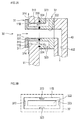
- FIG. 2A is an enlarged view showing the exhaust part 30, that is, the exhaust deposition preventing material 31 and the exhaust pipe connection part 32 when viewed from the side surface of the film forming container parallel to the gas flow direction.
- An opening 11A and an opening 11B are formed so that the gas flow in the exhaust gas deposition material 31 and the exhaust pipe connection portion 32 is parallel to the surface of the substrate 13.
- the atomic layer growth apparatus of this embodiment is a laminar flow type apparatus.
- the atomic layer growth apparatus is not limited to the laminar flow type.
- the exhaust adhesion preventing material 31 has a cylindrical hole 312 and a flange 311 having a size exceeding the opening 11B on the film forming container 11 side.
- the cylindrical adhesion-preventing material main body 310 located outside the flange 311 has a gap over the entire circumference with the inner peripheral surface of the opening 11B, and the gap constitutes the adhesion-inhibiting material inert gas supply path 313. is doing.
- the amount of the gap is not particularly limited in the present invention, but is preferably in the range of 0.01 to 5 mm, and is 1 mm in this embodiment.
- a gap is secured over the entire circumference between the inner surface of the flange 311 and the inner wall of the film forming container 11 around the opening 11B, and this gap is also part of the protective material inert gas supply path 313. Is configured.
- the gap between the flange 311 and the inner wall of the film forming container 11 may be intentionally provided, for example, 10 mm or less, and may be brought into contact with the inner wall of the film forming container 11 if the inner surface of the flange 311 is rough.
- the rough surface shape secures an inert gas supply path 313 for preventing deposition of gas. It is desirable that the protective material inert gas supply path 313 has at least 0.001 mm or more. The same applies to Embodiment 2 below.
- the protective material inert gas supply path 313 is partitioned from the cylindrical hole 312 constituting the exhaust hole by the peripheral wall of the protective material main body 310.
- the protective material inert gas outlet 314 has a shower head structure in which the protective material inert gas supply passages 313 are connected to a plurality of connection portion inert gas supply passages 323 as described later.
- the cylindrical exhaust pipe connecting portion 32 has an outer peripheral shape exceeding the opening portion 11 ⁇ / b> B and a cylindrical hole 322 along the axial direction, and communicates with the cylindrical hole 312 of the exhaust deposition preventive material 31.
- the cylinder holes 312 and 322 constitute exhaust holes.
- it can be set as the structure which does not become an exhaust hole itself but has an exhaust hole inside it. It is desirable that the connecting portion between the cylindrical hole 312 and the cylindrical hole 322 be formed flush.
- the exhaust pipe connection portion 32 is attached to the outer wall of the film forming container 11.
- an O-ring 330 is interposed between the distal end surface of the exhaust pipe connection portion 32 and the outer wall surface of the film forming container 11 to enhance the sealing performance.
- the front end surface of the exhaust deposition preventive material 31 is positioned so as to follow the outer wall of the film forming container 11 in the attached state. As a result, the distal end surface of the exhaust pipe connection portion 32 and the distal end surface of the exhaust gas deposition material 31 are brought together.
- an O-ring 331 is interposed between the front end surfaces to improve the sealing performance.
- An O-ring groove (not shown) for storing the O-ring 331 may be formed only in the exhaust gas-proofing material 31 for maintainability.
- FIG. 2B is a view of the exhaust pipe connecting portion 32 viewed from the inside of the film forming container, with the exhaust deposition preventing material 31 omitted.
- the connection part inert gas supply path 323 is formed along the axial direction of the exhaust pipe connection part 32 along the gas flow direction, and changes its direction in the outer circumferential direction in the middle of the axial direction. Open to the outer peripheral surface.
- each connection part inert gas supply path 323 is formed in the position where the hole surface of an outer peripheral side follows the hole surface of the opening part 11B, and is connected to the protection material inert gas supply path 313. .
- An end portion where the connection part inert gas supply path 323 communicates with the deposition material inert gas supply path 313 constitutes a connection part inert gas supply port 324.
- the cross-sectional shape of the connection part inert gas supply path 323 is not necessarily along the hole surface of the opening 11B.
- the connection part inert gas supply path 323 is partitioned from a cylindrical hole 322 that constitutes an exhaust hole by the inner peripheral wall of the exhaust pipe connection part 32.
- connection part inert gas supply path has one or more places in the exhaust pipe connection part.
- the exhaust pipe connection portion is provided at two locations on the upper side and the lower side, and the shower head structure is formed on the discharge port side It is preferable.
- the gas can be uniformly supplied to the protective material inert gas supply path or the protective material inert gas discharge port. Even when the exhaust pipe connection portion is circular, by providing a plurality of inert gas supply passages, the pressure uniformity in the protective material inert gas supply passage or the protective material inert gas discharge port is improved.
- the exhaust pipe connection portion 32 is connected to an exhaust pipe 40 having an exhaust hole 402 so as to communicate with the cylindrical hole 322.
- the gas exhausted from the film forming container 11 is discharged out of the film forming container 11 through the cylindrical holes 312 and 322 and the exhaust hole 402.
- an inert gas is supplied to the connection portion inert gas supply path 323 from an inert gas supply portion (not shown), and the inert gas passes through the plurality of connection portion inert gas supply paths 323 and is connected to the exhaust gas deposition preventive material.
- the inert gas is discharged into the film forming container 11 from the deposition material inert gas discharge port 314 through the connection portion inert gas supply port 324 and the deposition material inert gas supply path 313.
- nitrogen or argon can be used as the inert gas.
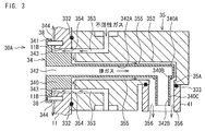
- the exhaust part 30 ⁇ / b> A of this embodiment is attached to the exhaust opening 11 ⁇ / b> B provided in the film forming container 11 as in the first embodiment.
- the exhaust part 30 ⁇ / b> A has a cylindrical exhaust deposition preventing material 34 and a cylindrical exhaust pipe connection part 35.
- the exhaust adhesion preventing material 34 has a cylindrical hole 342 and a flange 341 having a size exceeding the opening 11 ⁇ / b> B on the film forming container 11 side.
- a shim having a thickness of 2 mm is inserted into the flange 341 and the inner wall of the film forming container 11 and fixed with screws 38. Screws 38 are used at a plurality of locations. The number is not particularly limited.
- the cylindrical adhesion-preventing material body 340 located outside the flange 341 has a gap over the entire circumference of the inner peripheral surface of the opening 11B in the axial range of the opening 11B.
- a material inert gas supply path 343 is configured.
- the amount of the gap is not particularly limited in the present invention, but is preferably in the range of 0.01 to 5 mm. In this embodiment, it is 1 mm.
- a gap is secured over the entire circumference between the inner surface of the flange 341 and the inner wall of the film forming container 11 around the opening 11B, and this gap is also a part of the deposition material inert gas supply path 343.
- the gap between the flange 341 and the inner wall of the film forming container 11 may be intentionally provided, for example, 10 mm or less, and may be brought into contact with the inner wall of the film forming container 11 if the inner surface of the flange 341 is rough.
- the rough surface shape secures an inert gas supply path 343 for preventing deposition of gas. It is desirable that the protective material inert gas supply path 343 has at least 0.001 mm or more.
- a clearance over the entire circumference between the inner peripheral surface of the flange 341 and the inner wall of the film forming container 11 constitutes an adhesion preventing material inert gas discharge port 344.
- the protective material inert gas supply path 343 is partitioned from the cylindrical hole 342 by the peripheral wall of the cylindrical protective material main body 340.
- the protective material inert gas discharge port 344 has a shower head structure in which the protective material inert gas supply path 343 is connected to a plurality of connection portion inert gas supply paths 353 as described later. Yes.
- the exhaust prevention material 34 has a prevention exhaust pipe 340 ⁇ / b> A that is continuous with the inner peripheral side of the exhaust prevention material main body 340 and extends outward in the axial direction, and the tube hole 342 ⁇ / b> A communicates with the tube hole 342. ing.
- the cylindrical exhaust pipe connecting portion 35 has an outer peripheral shape exceeding the opening 11B and a cylindrical hole 352 along the axial direction.
- the exhaust pipe connecting portion 35 is attached to the outer wall of the film forming container 11.
- an O-ring 332 is interposed between the front end surface of the exhaust pipe connecting portion 35 and the outer wall surface of the film forming container 11.
- the sealing property is improved.
- the tip end surface of the exhaust gas deposition preventive material 34 is positioned so as to follow the outer wall surface of the film forming container after being attached. As a result, the distal end surface of the exhaust pipe connecting portion 35 and the distal end surface of the exhaust gas deposition material 34 are brought into contact with each other.
- connection portion inert gas supply paths 353 are formed on the periphery of the outer periphery of the cylindrical hole 352, on the exhaust adhesion prevention material 34 side, on the upper side, the lower side, and both side sides, respectively. .
- the connection part inert gas supply path 353 is formed along the axial direction of the exhaust pipe connection part 35 along the gas flow direction, and changes its direction in the outer circumferential direction at a position close to the front in the axial direction, respectively. 35 is open to the outer peripheral surface.
- each connection part inert gas supply path 353 is formed in the position where the hole surface of an outer peripheral side follows the hole surface of the opening part 11B, and is connected to the protection material inert gas supply path 343. .
- An end portion where the connection part inert gas supply path 353 communicates with the deposition material inert gas supply path 343 constitutes a connection part inert gas supply port 354.
- the cross-sectional shape of the connection portion inert gas supply path 353 is not necessarily along the hole surface of the opening 11B.
- the connection part inert gas supply path 353 is partitioned from a cylindrical hole 342 constituting an exhaust hole by the peripheral wall of the exhaust pipe connection part 35 and the deposition exhaust pipe 340A.
- the cylindrical hole 352 is closed at the outer end of the exhaust pipe connection portion 35, and communicates from the side with an attachment hole 35 ⁇ / b> A opened to the side.
- the deposition prevention exhaust pipe 340A extends with a small gap until just before reaching the end, and the end is closed, and near the end, the attachment hole is formed on the side of the protection exhaust pipe 340A.
- a connection hole 340B facing 35A is formed.
- a clearance is provided between the outer peripheral surface of the deposition preventing exhaust pipe 340 ⁇ / b> A and the inner peripheral surface of the cylindrical hole 352 of the exhaust piping connection portion 35, and the clearance constitutes the connection portion inert gas second supply path 355. is doing.
- connection part inert gas second supply path 355 is a connection path connecting to the connection part inert gas supply path 353 at the front surface of the exhaust pipe connection part 35 on the film forming container side and in contact with the exhaust gas prevention material 34. have.
- the ratio of the total gas conductance between the protective material inert gas supply path 343 and the connection part inert gas second supply path 355 is preferably 0.01 to 100, more preferably 1: 1. . This is because an equal amount of inert gas is supplied to the film forming container 11 side and the exhaust pipe 41 side.
- the gas conductance can be controlled by the channel width and channel length of the inert gas supply channel.
- an exhaust pipe 41 is attached to the attachment hole 35A, and an O-ring 333 is interposed between the joint surfaces of both to enhance sealing performance.
- a prevention exhaust extension pipe 340C extending in the direction of the exhaust pipe 41 is connected to the connecting hole 340B.
- the attachment exhaust extension pipe 340 ⁇ / b> C can be easily attached from the attachment side of the exhaust pipe 41 through the attachment hole 35 ⁇ / b> A in a state where the exhaust pipe 41 is removed from the exhaust pipe connection portion 35.
- the tube hole 342B of the deposition-proof exhaust extension tube 340C communicates with the tube hole 342A and the tube hole 342.
- the partial inert gas second supply path 355 extends.
- the connection part inert gas second supply path 355 at the tip position of the deposition preventing extension pipe 340 ⁇ / b> C constitutes a connection part inert gas second supply port 356.
- the exhaust pipe 41 for example, a pipe having an inner diameter of 150 mm can be used.
- a cylinder having an inner diameter of 100 mm and a height of 100 mm can be used as the deposition preventing exhaust extension pipe 340C, and it is desirable to have a flange so that it can be fixed to the deposition preventing exhaust pipe 340A with screws.
- the attachment of the prevention exhaust pipe 340C becomes possible after the attachment prevention exhaust pipe 340A is attached to the film forming container opening 11B side and then the exhaust pipe 41 is removed.
- the gas exhausted from the film forming container 11 is discharged out of the film forming container 11 through the cylindrical hole 342 and the tube holes 342A and 342B.
- the tube hole 342 and the tube holes 342A and 342B constitute an exhaust hole.
- an inert gas is supplied to the connection portion inert gas supply path 353 from an inert gas supply portion (not shown), and the inert gas passes through the plurality of connection portion inert gas supply paths 353 and is used as an exhaust gas deposition preventive material.
- the inert gas is discharged into the film forming container 11 from the deposition material inert gas outlet 344 through the connection portion inert gas supply port 354 and the deposition material inert gas supply path 343.
- nitrogen or argon can be used as the inert gas.
- the inert gas By the discharge of the inert gas, film formation in the gaps between the exhaust deposition preventive material 34, the opening 11B, and the exhaust pipe connection portion 35 is suppressed. Further, the cylinder hole side of the exhaust pipe connection portion 35 is covered with the deposition preventing exhaust pipe 340A, and film formation is prevented. Further, a part of the inert gas sent to the connection part inert gas supply path 353 is sent to the connection part inert gas second supply path 355, and the adhesion prevention exhaust pipe 340A and the adhesion prevention exhaust extension pipe 340C are connected.
- the gas is discharged along the pipe direction of the exhaust pipe 41 from the tip of the deposition-proof exhaust extension pipe 340C through the periphery of the connection part and the periphery of the connection part of the exhaust pipe connection part 35 and the exhaust pipe 41.
- By discharging the inert gas it is possible to suppress film formation in the gap between the deposition prevention exhaust pipe 340A and the exhaust pipe connection portion 35 and the gap between the deposition prevention exhaust pipe 340A and the extension pipe 340C.
- the opening 11B and the exhaust pipe connecting portion 35 can be made maintenance-free.
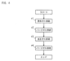
- FIG. 4 is a flowchart showing an example of the atomic layer deposition method of this embodiment.
- 5A to 5D are diagrams showing a process of forming a thin film on the substrate S.
- FIG. 4 is a flowchart showing an example of the atomic layer deposition method of this embodiment.
- 5A to 5D are diagrams showing a process of forming a thin film on the substrate S.
- FIG. 4 is a flowchart showing an example of the atomic layer deposition method of this embodiment.
- 5A to 5D are diagrams showing a process of forming a thin film on the substrate S.
- the source gas supply unit supplies source gas into the film formation container 11 (step s1). Specifically, the source gas is supplied to the gas introduction unit 20 (step s1). The source gas is supplied into the film forming container 11. The source gas is supplied into the film forming container 11 for 0.1 seconds, for example. As shown in FIG. 5A, in step s1, the source gas 110 is supplied to the inside of the film forming container 11, and the source gas 110 is adsorbed on the substrate S, so that the adsorption layer 102 is formed.
- step s 1 an inert gas is supplied to the inner surface of the injector 21 and the outer surface of the injector deposition preventing material 22. Moreover, in the exhaust part 30, an inert gas is supplied also to an exhaust pipe connection part and an exhaust adhesion preventing material. In the present embodiment, the inert gas is always supplied not only in step s1, but also in steps s2 to 4 described later. Therefore, when supplying the source gas into the film forming container 11 in step s1, the raw material is formed in the gap between the film forming container 11 and the injector deposition preventing material 22 and the gap between the film forming container 11 and the exhaust deposition preventing material 31. Gas can be prevented from entering.
- the supply of the source gas is stopped, and the purge gas is supplied at the gas introduction part (step s2).
- the purge gas is supplied into the film forming container 11.
- the source gas is discharged from the exhaust unit 30 to the outside of the film forming container 11.
- the purge gas is supplied into the film forming container 11 for 0.1 seconds, for example.
- the exhaust unit 30 exhausts the source gas 110 and the purge gas 112 inside the film formation container 11.
- the exhaust unit 30 exhausts the source gas 110 and the purge gas 112 inside the film formation container 11 for 2 seconds, for example.
- the purge gas 112 is supplied to the inside of the film forming container 11 and the source gas 110 not adsorbed on the substrate S is purged from the film forming container 11 in step s2.
- a reactive gas is supplied into the film formation container 11 (step s3).
- the reaction gas is supplied through the gas introduction unit 20 (step s3).
- the reaction gas is supplied to the inside of the film forming container 11 through the passage of the gas introduction unit 20.
- the reaction gas is supplied into the film formation container 11 for 1 second, for example.
- the reaction gas 114 is supplied into the film formation container 11 in step s3.
- step s3 an inert gas is supplied from the inner surface of the injector 21, the outer surface of the injector deposition material 22, and the exhaust part 30. Therefore, when the reaction gas is supplied into the film formation container 11 in step s3, the reaction occurs in the gap between the film formation container 11 and the injector adhesion preventing material 22 and the gap between the film formation container 11 and the exhaust adhesion preventing material 31. Gas can be prevented from entering.
- step s4 the supply of the reaction gas is stopped, and the purge gas is supplied to the gas introduction unit 20 (step s4).
- the purge gas is supplied into the film forming container 11.
- the purge gas is discharged from the exhaust unit 30 to the outside of the film formation container 11.
- the purge gas is supplied into the film forming container 11 for 0.1 seconds, for example.
- the exhaust unit 30 exhausts the reaction gas 114 and the purge gas 112 inside the film formation container 11. As shown in FIG. 5D, in step s 4, the purge gas 112 is supplied into the film formation container 11 and the reaction gas 114 is purged from the film formation container 11.
- the thin film layer 104 for one atomic layer is formed on the substrate S by the steps s1 to s4 described above. Thereafter, the thin film layer 104 having a desired film thickness can be formed by repeating steps s1 to s4 a predetermined number of times.
- the source gas and the reactive gas are in the gap between the film forming container 11 and the injector 21. Intrusion can be suppressed. Therefore, it is possible to suppress the thin film from adhering to the gap between the film forming container 11 and the injector 21. Similarly, the exhaust portion 30 is also prevented from attaching a thin film.
- an alumina film formed using TMA as a source gas and O 3 as a reaction gas can be subjected to gas etching using BCl 3 gas.
- gas-etch the alumina film with BCl 3 gas it is necessary to heat it to a high temperature of about 500 ° C., for example.
- the inner wall of the film forming container 11 located in the vicinity of the heater 14A can be heated to a high temperature of about 500 ° C. by the heater 14A. Therefore, the thin film adhering to the inner wall of the film forming container 11 located in the vicinity of the heater 14A can be removed by gas etching.
- An AlON thin film was formed on a 370 mm ⁇ 470 mm G2 glass substrate using the structure of the film forming container 11 of Embodiment 1 and the exhaust part 30A shown in FIG. TMA (trimethylaluminum) was used as the liquid source (Al source), and oxygen plasma and nitrogen plasma were used as the reaction gas.
- TMA trimethylaluminum
- Al source oxygen plasma and nitrogen plasma were used as the reaction gas.
- the film formation was performed in the sequence shown in FIG.
- the inert gas was supplied at a flow rate of 500 sccm (80 ° C.) and was always supplied during the film forming sequence.
- the protective material inert gas supply path, the connection part inert gas supply path, the exhaust gas protection material corresponding to the connection part inert gas second supply path part, and the film on the inner wall of the exhaust pipe connection part When the thickness was visually observed, the interference film of the AlON thin film visually observed was not observed, and it was confirmed that the deposition amount was 50 nm or less.
- the maintenance of the exhaust part is only the exhaust prevention material and screw, the exhaust pipe, and the prevention exhaust extension pipe, and the opening part and the exhaust pipe connection part can be made maintenance-free.
Landscapes
- Chemical & Material Sciences (AREA)
- General Chemical & Material Sciences (AREA)
- Chemical Kinetics & Catalysis (AREA)
- Engineering & Computer Science (AREA)
- Materials Engineering (AREA)
- Mechanical Engineering (AREA)
- Metallurgy (AREA)
- Organic Chemistry (AREA)
- Chemical Vapour Deposition (AREA)
Abstract
成膜容器に設けられた排気用の開口部の外側に取り付けられ、外周面が開口部を超える大きさを有し、筒穴側に排気路が位置する筒状の排気配管接続部と、 成膜容器内側に位置して開口部に挿入して取り付けられ、筒穴側に排気路が位置する筒状の排気防着材を備え、排気配管接続部に、排気路と区画されて、不活性ガスが流れる接続部不活性ガス供給路と、接続部不活性ガス供給路に設けられて不活性ガスが開口部側に流れ出る接続部不活性ガス供給口が設けられ、排気防着材に排気路と区画されて、開口部内周面および開口部周りの成膜容器内壁と防着材の間の隙間により形成され、接続部不活性ガス供給口に連通する防着材不活性ガス供給路と、防着材不活性ガス供給路に設けられて不活性ガスが成膜容器内部に流れ出る防着材不活性ガス排出口を設ける。
Description
本発明は、基板上に薄膜を形成する原子層成長装置に関する。
原子層成長法は、形成しようとする薄膜を構成する元素のガスを基板上に交互に供給し、基板上に原子層単位で薄膜を形成するもので、薄膜を均一に形成する技術として知られている。原子層成長法は、一般的なCVD(Chemical Vapor Deposition)法と比較して、段差被覆性や膜厚制御性に優れている。
原子層成長法により薄膜の形成を繰り返し行うと、成膜容器の内表面にも薄膜が付着する。成膜容器内表面に付着した薄膜の厚さが厚くなると、堆積した薄膜が剥離し、その一部分がパーティクルとなり、基板上に形成される薄膜の質が劣化する原因となる。そのため、成膜容器の内表面に付着した薄膜を定期的に除去することが好ましい。
原子層成長法により薄膜の形成を繰り返し行うと、成膜容器の内表面にも薄膜が付着する。成膜容器内表面に付着した薄膜の厚さが厚くなると、堆積した薄膜が剥離し、その一部分がパーティクルとなり、基板上に形成される薄膜の質が劣化する原因となる。そのため、成膜容器の内表面に付着した薄膜を定期的に除去することが好ましい。
特許文献1では、CVD成膜やスパッタ成膜などの気相成長装置において、防着板を使用するとともに、さらに、チャンバの内壁に堆積した堆積物を非晶質膜で覆う処理方法および装置が提案されている。
さらに、特許文献2では、ALD(Atomic Layer Deposition)真空成膜装置において、反応室から排出される原料ガスが通過する排気ボックスがその内部に防着板が挿入されて構成され、排気ボックスの内壁面にシール機構が設けられ、このシール機構は、中空のシール部材からなり、該シール部材の内部にガスを連続的に導入して膨張させると、該排気ボックスの内部に向かって膨張して、挿入された防着板の表面に当接し、該排気ボックスの内壁と防着板の表面との隙間をシールするよう構成され、このシール部材には、導入したガスを吐出するための少なくとも1つの孔が設けられているものが提案されている。
さらに、特許文献2では、ALD(Atomic Layer Deposition)真空成膜装置において、反応室から排出される原料ガスが通過する排気ボックスがその内部に防着板が挿入されて構成され、排気ボックスの内壁面にシール機構が設けられ、このシール機構は、中空のシール部材からなり、該シール部材の内部にガスを連続的に導入して膨張させると、該排気ボックスの内部に向かって膨張して、挿入された防着板の表面に当接し、該排気ボックスの内壁と防着板の表面との隙間をシールするよう構成され、このシール部材には、導入したガスを吐出するための少なくとも1つの孔が設けられているものが提案されている。
特許文献1では、従来の気相成長装置であれば、クリーニングの頻度を低減することは可能である。しかし、チャンバの内壁に堆積した堆積物や堆積物を覆う非晶質膜の厚さが所定の厚さ以上になった場合、ウェットエッチング方法を用いてクリーニングを行う必要がある。ウェットエッチング方法では、成膜容器を開放するため、成膜容器が大型になるにつれて、開放作業の手間が大きくなるため、ガスエッチング方法を用いることができる場合は、ガスエッチング方法を用いることが好ましい。しかし、ガスエッチング方法によりエッチングを行うためには、成膜容器の内壁面の薄膜の付着部分を所定の温度以上に加熱する必要があるが、ヒーターから離れた部分では、必要な加熱温度に達せず、ガスエッチングを行うのが困難になる。そのため、ガスエッチングを行いにくい場所にある程度の量の薄膜が付着した場合、成膜容器を開放してウェットエッチングを行う必要が生じるという問題がある。
ALD装置では、原料ガス及び反応ガスは微細な隙間へ容易に侵入し、膜を形成する。このような微細な隙間に侵入したガスは、膜や粉となり、パーティクルの要因となる。よって、防着板を利用し、防着板裏面に不活性ガスを供給することで成膜室、排気ボックス本体への着膜を抑制し、パーティクル発生を回避することが可能となる。特許文献2の手法によれば、排気ボックスの下流側から上流側への反応ガス進入を抑制することが可能であるが、成膜室と排気防着板の隙間や防着板を固定するビス穴から進入する反応ガスを抑制するのは困難となるため、成膜室側の排気ボックス導入口へ膜や粉が堆積し、パーティクルの要因となる。また、着膜抑制がトラップボックス中流部のみであるため、排気配管周辺のトラップボックス下流の着膜は回避することが不可能となるため、排気ボックスのメンテナンスも必要となる。
本発明は、排気側のクリーニングの頻度を低減し、メンテナンス作業性を向上させることができる原子層成長装置およびその排気部を提供することを目的の一つとする。
すなわち、本発明の原子層成長装置のうち、第1の形態は、
成膜容器と、
前記成膜容器に設けられた排気用の開口部の外側に取り付けられ、外周面が前記開口部を超える大きさを有し、筒穴側に排気路が位置する筒状の排気配管接続部と、
前記成膜容器内側に位置して前記開口部に挿入して取り付けられ、筒穴側に排気路が位置する筒状の排気防着材と、を備え、
前記排気配管接続部に、
前記排気路と区画されて、不活性ガスが流れる接続部不活性ガス供給路と、前記接続部不活性ガス供給路に設けられて前記不活性ガスが前記開口部側に流れ出る接続部不活性ガス供給口と、が設けられ、
前記排気防着材に、
前記排気路と区画されて、前記開口部内周面および前記開口部周りの前記成膜容器内壁と前記排気防着材の間の隙間により形成され、前記接続部不活性ガス供給口に連通する防着材不活性ガス供給路と、前記防着材不活性ガス供給路に設けられて前記不活性ガスが前記成膜容器内部に流れ出る防着材不活性ガス排出口と、が設けられていることを特徴とする。
成膜容器と、
前記成膜容器に設けられた排気用の開口部の外側に取り付けられ、外周面が前記開口部を超える大きさを有し、筒穴側に排気路が位置する筒状の排気配管接続部と、
前記成膜容器内側に位置して前記開口部に挿入して取り付けられ、筒穴側に排気路が位置する筒状の排気防着材と、を備え、
前記排気配管接続部に、
前記排気路と区画されて、不活性ガスが流れる接続部不活性ガス供給路と、前記接続部不活性ガス供給路に設けられて前記不活性ガスが前記開口部側に流れ出る接続部不活性ガス供給口と、が設けられ、
前記排気防着材に、
前記排気路と区画されて、前記開口部内周面および前記開口部周りの前記成膜容器内壁と前記排気防着材の間の隙間により形成され、前記接続部不活性ガス供給口に連通する防着材不活性ガス供給路と、前記防着材不活性ガス供給路に設けられて前記不活性ガスが前記成膜容器内部に流れ出る防着材不活性ガス排出口と、が設けられていることを特徴とする。
上記形態の本発明によれば、接続部不活性ガス供給路を流れる不活性ガスが防着材不活性ガス供給路に流れ、防着材不活性ガス排出口に流れ出すことで、排気防着材と成膜容器内壁や開口部、排気配管接続部との隙間に着膜が生じるのを抑止する。
第2の形態の本発明の原子層成長装置は、前記本発明の形態において、前記防着材不活性ガス排出口が、前記排気防着材の全周に亘って形成されていることを特徴とする。
上記形態の本発明によれば、排気防着材と成膜容器内壁との隙間に着膜を生じるのを全周に亘り確実に防止することができる。
第3の形態の本発明の原子層成長装置は、前記本発明の形態において、前記開口部の内周面と前記開口部に挿入された前記排気防着材の外周面との間の隙間が、10mm以下であることを特徴とする。
上記形態の本発明によれば、開口部の内周面と開口部に挿入された防着材外周面との間の隙間を適切に確保することで、不活性ガスの流れを確実に確保して着膜を防止し、適正なガスの流速を得ることを容易にする。この隙間は、10mm以下が望ましい。上記隙間が10mmを超えると、適正な流速を得るためにガスの流量が多く必要になる。5mm以下が一層望ましい。隙間の下限は特に限定されず、不活性ガスの流出が得られるものであればよい。部材同士を当接させる場合にも、粗面同士であれば、その隙間によりガス流出が得られる。例えば、防着材外周面を、敢えて粗面(例えばRa(算術平均粗さ)=3~6μm)として、防着材外周面を成膜容器に当接させて取り付けるようにしてもよい。この点で、隙間の下限は、0.01mmを例示することができる。
第4の形態の本発明の原子層成長装置は、前記本発明の形態において、前記開口部の周りの前記成膜容器内壁と前記排気防着材との間の隙間が、10mm以下であることを特徴とする。
上記形態の本発明によれば、開口部の周りの成膜容器内壁と防着材との間の隙間により、不活性ガスの流れを確実に確保して着膜を防止し、適正なガスの流速を得ることを容易にする。上記隙間が10mmを超えると、ガスの流れが十分に得られない。一方、隙間の下限は特に限定されず、ガスの流出が得られるものであればよい。部材同士を当接させる場合にも、粗面同士であれば、その隙間によりガス流出が得られる。この点で、隙間の下限は、0.001mm以上を例示することができる。
第5の形態の本発明の原子層成長装置は、前記本発明の形態において、前記接続部不活性ガス供給路は、前記排気路の外周側で、排気ガスの流れ方向に沿って1または複数が設けられていることを特徴とする。
上記形態の本発明によれば、1または複数の接続部不活性ガス供給路を通して、不活性ガスを供給することができる。特に複数を設ければ、できるだけ均等にガスを供給することができる。複数の接続部不活性ガス供給路は、例えば、少なくとも排気穴の上方、下方、両側方に設けることができる。
第6の形態の本発明の原子層成長装置は、前記本発明の形態において、前記排気防着材は、前記排気配管接続部の筒穴内に挿入され、前記筒穴に沿って伸長する防着排気配管を有し、該防着排気配管は前記排気防着材の筒穴に連通しており、前記筒穴および前記防着排気配管の管穴が、長さ方向において前記排気路の少なくとも一部を構成していることを特徴とする。
上記形態の本発明によれば、防着排気配管の配置により、排気防着材と排気配管接続部との隙間および排気配管接続部の内周面が覆われて着膜が防止される。
第7の形態の本発明の原子層成長装置は、前記本発明の形態において、前記防着排気配管と前記排気配管接続部の筒穴との間に、前記防着排気配管の先端に至る接続部不活性ガス第2供給路を有し、該接続部不活性ガス第2供給路の先端側に、不活性ガスが流れ出る接続部不活性ガス第2供給口が設けられていることを特徴とする。
上記形態の本発明によれば、接続部不活性ガス第2供給路によって、防着排気配管の先端側への着膜を抑止され、排気配管接続部への着膜を抑止する。
第8の形態の本発明の原子層成長装置は、前記本発明の形態において、前記接続部不活性ガス第2供給路が前記接続部不活性ガス供給路に連通していることを特徴とする。
上記形態の本発明によれば、接続部不活性ガス供給路に供給された不活性ガスの一部を接続部不活性ガス第2供給路に送り出すことができる。
第9の形態の本発明の原子層成長装置は、前記本発明の形態において、前記排気配管接続部に排気配管が接続されていることを特徴とする。
上記形態の本発明によれば、排気配管を通して排ガスを移送することができる。
排気配管は、排気配管接続部に取り付け可能なものであってもよく、また、排気配管接続部に排気配管が一体になって接続されているものであってもよい。
排気配管は、排気配管接続部に取り付け可能なものであってもよく、また、排気配管接続部に排気配管が一体になって接続されているものであってもよい。
第10の形態の本発明の原子層成長装置は、前記本発明の形態において、前記防着排気配管は、前記排気配管接続部に接続された前記排気配管内に挿入される長さを有していることを特徴とする。
上記形態の本発明によれば、排気配管接続部での着膜を抑止する。
第11の形態の本発明の原子層成長装置は、前記本発明の形態において、前記防着排気配管は、防着排気延長管を有し、該防着排気延長管は前記排気配管に挿入される長さを有し、前記防着排気延長管は、前記排気配管が接続される側から取り付け可能であることを特徴とする。
上記形態の本発明によれば、防着排気配管の長さを延長管で調整することができ、排気配管との接続側から容易に取り付けすることができる。
第12の形態の本発明の原子層成長装置は、前記本発明の形態において、前記防着排気配管外周面は、前記排気配管内周面と隙間を有していることを特徴とする。
上記形態の本発明によれば、防着排気配管と排気配管との幅方向の隙間によって、接続部不活性ガス供給路の一部を構成することができ、防着排気配管と排気配管との接続隙間への着膜を防止することができる。結果、排気配管接続部への着膜を抑止することができる。
第13の形態の本発明の原子層成長装置は、前記本発明の形態において、前記排気防着材は、前記開口部の周りの前記成膜容器内壁に沿い、かつ前記内壁と間隙を有するフランジを有しており、該フランジ周縁内面と前記成膜容器内壁との間に前記防着材不活性ガス排出口が設けられていることを特徴とする。
上記形態の本発明によれば、フランジ周辺から側方に不活性ガスを排出することができ、粒子などが排ガス方向に沿って内部に侵入するのを抑止する。
本発明の原子層成長装置排気部は、
成膜容器に設けられた排気用の開口部の外側に取り付けられ、外周面が前記開口部を超える大きさを有し、筒穴側に排気路が位置する筒状の排気配管接続部と、
前記成膜容器内側に位置して前記開口部に挿入して取り付けられ、筒穴側に排気路が位置する筒状の排気防着材と、を備え、
前記排気配管接続部に、
前記排気路と区画されて、不活性ガスが流れる接続部不活性ガス供給路と、前記接続部不活性ガス供給路に設けられて前記不活性ガスが前記開口部側に流れ出る接続部不活性ガス供給口と、が設けられ、
前記排気防着材に、
前記排気路と区画されて、前記開口部内周面および前記開口部周りの前記成膜容器内壁と前記排気防着材の間の隙間により形成され、前記接続部不活性ガス供給口に連通する防着材不活性ガス供給路と、前記防着材不活性ガス供給路に設けられて前記不活性ガスが前記成膜容器内部に流れ出る防着材不活性ガス排出口と、が設けられていることを特徴とする。
成膜容器に設けられた排気用の開口部の外側に取り付けられ、外周面が前記開口部を超える大きさを有し、筒穴側に排気路が位置する筒状の排気配管接続部と、
前記成膜容器内側に位置して前記開口部に挿入して取り付けられ、筒穴側に排気路が位置する筒状の排気防着材と、を備え、
前記排気配管接続部に、
前記排気路と区画されて、不活性ガスが流れる接続部不活性ガス供給路と、前記接続部不活性ガス供給路に設けられて前記不活性ガスが前記開口部側に流れ出る接続部不活性ガス供給口と、が設けられ、
前記排気防着材に、
前記排気路と区画されて、前記開口部内周面および前記開口部周りの前記成膜容器内壁と前記排気防着材の間の隙間により形成され、前記接続部不活性ガス供給口に連通する防着材不活性ガス供給路と、前記防着材不活性ガス供給路に設けられて前記不活性ガスが前記成膜容器内部に流れ出る防着材不活性ガス排出口と、が設けられていることを特徴とする。
本発明によれば、排気防着材を成膜容器内側から簡単に取り外すことが可能であり、排気防着材と成膜容器の隙間及び、排気防着材と排気配管接続部の隙間に不活性ガスパージを行うことができ、成膜容器及び排気配管接続部への着膜を抑制することが可能となる。これにより、パーティクル発生の抑制と成膜容器及び排気配管接続部のクリーニング頻度低減が可能となる。
(実施形態1)
まず、図1を参照して、本実施形態の原子層成長装置の構成を説明する。
図1は、本実施形態の原子層成長装置の一例を示す概略構成図である。
本実施形態の原子層成長装置10は、原料ガスと反応ガスとを交互に供給し、基板13上に原子層単位で薄膜を形成する。その際、反応活性を高めるため、基板13を加熱させることができる。特に、本実施形態では原料ガスとしてTMA(Tri-Methyl Aluminum)を用い、その際、反応活性を高めるため、プラズマを発生させることもできる。本実施形態では、プラズマの発生に平行平板電極を用いるが、この方式に限定されない。
まず、図1を参照して、本実施形態の原子層成長装置の構成を説明する。
図1は、本実施形態の原子層成長装置の一例を示す概略構成図である。
本実施形態の原子層成長装置10は、原料ガスと反応ガスとを交互に供給し、基板13上に原子層単位で薄膜を形成する。その際、反応活性を高めるため、基板13を加熱させることができる。特に、本実施形態では原料ガスとしてTMA(Tri-Methyl Aluminum)を用い、その際、反応活性を高めるため、プラズマを発生させることもできる。本実施形態では、プラズマの発生に平行平板電極を用いるが、この方式に限定されない。
成膜容器11は、ガス導入部20と、排気部30と、ヒーター14Aを有するステージ14と、上部電極12と、高周波電源15と、を備える。ヒーター14Aにより、基板13の温度を調整することができる。例えば、プラズマALDの場合、基板13を50~200℃に加熱することができる。
上部電極12は、ステージ14上に設置した基板13の上方に位置するように設けられ、高周波電源15と接続されている。高周波電源15が所定の周波数の高周波電流を供給することにより、上部電極12とステージ14との間でプラズマが生成される。
上部電極12は、ステージ14上に設置した基板13の上方に位置するように設けられ、高周波電源15と接続されている。高周波電源15が所定の周波数の高周波電流を供給することにより、上部電極12とステージ14との間でプラズマが生成される。
成膜容器11では、ガス導入が行われる開口部11Aに、ガス導入部20が設けられている。ガス導入部20では、成膜容器11外側に筒状のインジェクタ21が配置され、成膜容器11内側から筒状のインジェクタ防着材22が開口部11A内に挿入されて取り付けられている。インジェクタ21とインジェクタ防着材22とは、ガス通路が設けられており、互いに付き合わせて設置されている。ガス通路の数は特に限定されるものではない。
ガス導入部20では、原料ガス、反応ガス、パージガスを成膜容器11内に供給する。
ガス導入部20では、原料ガス、反応ガス、パージガスを成膜容器11内に供給する。
また、成膜容器11では、ガス排出が行われる開口部11Bに、排気部30が設けられている。排気部30では、成膜容器11内側から筒状の排気防着材31が開口部11B内に挿入されて取り付けられ、成膜容器11外側に筒状の排気配管接続部32が取り付けられている。排気配管接続部32には、排気配管40が接続される。
図2Aは、ガス流れ方向に平行な成膜容器側面から見た場合の排気部30、すなわち排気防着材31および排気配管接続部32を示す拡大図である。
排気防着材31および排気配管接続部32のガスの流れは、基板13面に平行になるように開口部11Aおよび開口部11Bが形成されている。すなわち、この実施形態の原子層成長装置は、ラミナーフロー型の装置である。ただし、本発明としては、原子層成長装置がラミナーフロー型に限定されるものではない。
排気防着材31および排気配管接続部32のガスの流れは、基板13面に平行になるように開口部11Aおよび開口部11Bが形成されている。すなわち、この実施形態の原子層成長装置は、ラミナーフロー型の装置である。ただし、本発明としては、原子層成長装置がラミナーフロー型に限定されるものではない。
排気防着材31には、図2Aに示すように、筒穴312を有し、成膜容器11側に開口部11Bを超える大きさのフランジ311を有している。
フランジ311の外側に位置する筒状の防着材本体310は、開口部11B内周面と全周に亘って隙間を有しており、該隙間が防着材不活性ガス供給路313を構成している。この隙間の量は、本発明としては特に限定されるものではないが、0.01~5mmの範囲が好適であり、この実施形態では1mmとする。
フランジ311の外側に位置する筒状の防着材本体310は、開口部11B内周面と全周に亘って隙間を有しており、該隙間が防着材不活性ガス供給路313を構成している。この隙間の量は、本発明としては特に限定されるものではないが、0.01~5mmの範囲が好適であり、この実施形態では1mmとする。
また、フランジ311の内面と開口部11Bの周りの成膜容器11内壁との間には全周に亘って隙間が確保されており、該隙間も防着材不活性ガス供給路313の一部を構成している。フランジ311と成膜容器11内壁との隙間は、意図的に例えば10mm以下で設けてもよく、フランジ311の内面が粗面であれば、成膜容器11内壁に当接させてもよい。
例えば、フランジ311の内面を、敢えて粗面とし(例えばRa(算術平均粗さ)=3~6μm)として、フランジ311内面を成膜容器11内壁に当接させて取り付けるようにしてもよい。
この粗面形状によってガスが流れる防着材不活性ガス供給路313が確保される。防着材不活性ガス供給路313は、少なくとも0.001mm以上を有するのが望ましい。
以下の実施形態2でも同様である。
例えば、フランジ311の内面を、敢えて粗面とし(例えばRa(算術平均粗さ)=3~6μm)として、フランジ311内面を成膜容器11内壁に当接させて取り付けるようにしてもよい。
この粗面形状によってガスが流れる防着材不活性ガス供給路313が確保される。防着材不活性ガス供給路313は、少なくとも0.001mm以上を有するのが望ましい。
以下の実施形態2でも同様である。
フランジ311周縁内面と成膜容器11内壁との全周に亘る隙間は、防着材不活性ガス排出口314を構成する。
なお、防着材不活性ガス供給路313は、防着材本体310の周壁によって、排気穴を構成する筒穴312とは区画されている。
防着材不活性ガス排出口314は、後述するように、防着材不活性ガス供給路313が複数本の接続部不活性ガス供給路323に接続されたシャワーヘッド構造を有している。
なお、防着材不活性ガス供給路313は、防着材本体310の周壁によって、排気穴を構成する筒穴312とは区画されている。
防着材不活性ガス排出口314は、後述するように、防着材不活性ガス供給路313が複数本の接続部不活性ガス供給路323に接続されたシャワーヘッド構造を有している。
筒状の排気配管接続部32は、開口部11Bを超える外周形状と、軸方向に沿った筒穴322を有しており、排気防着材31の筒穴312に連通している。この実施形態では、筒穴312、322は排気穴を構成する。なお、筒穴そのものが排気穴とならず、その内側に排気穴を有する構成とすることができる。筒穴312と筒穴322との接続部分は、面一に形成するのが望ましい。
排気配管接続部32は、成膜容器11の外壁に取り付けられる。取り付けに際しては、排気配管接続部32の先端面と成膜容器11の外壁面との間には、Oリング330を介在させて封止性を高めている。また、排気防着材31の先端面は、取り付けた状態で、成膜容器11の外壁に倣うように位置する。これにより排気配管接続部32の先端面と排気防着材31の先端面とが付き合わせ状態になる。その際に、先端面間にOリング331を介在させてシール性を高めている。Oリング331を収納するOリング溝(図示しない)は、メンテナンス性のため排気防着材31のみに形成するようにしてもよい。
また、排気配管接続部32では、図2Bに示すように、筒穴322の周囲に、開口部11Bの内周面に外側の穴面が沿うように、上方側、下方側、両側方側に、それぞれ接続部不活性ガス供給路323が設けられている。図2Bは、排気防着材31を省略して、成膜容器内側から排気配管接続部32を見た図である。
接続部不活性ガス供給路323は、ガスの流れ方向に沿って排気配管接続部32の軸方向に沿って形成され、軸方向中程でそれぞれ外周方向に向きを変えて排気配管接続部32の外周面に開口している。
接続部不活性ガス供給路323は、ガスの流れ方向に沿って排気配管接続部32の軸方向に沿って形成され、軸方向中程でそれぞれ外周方向に向きを変えて排気配管接続部32の外周面に開口している。
また、各接続部不活性ガス供給路323は、外周側の穴面が開口部11Bの穴面に沿う位置に形成されており、かつ、防着材不活性ガス供給路313に連通している。接続部不活性ガス供給路323が防着材不活性ガス供給路313に連通する端部は、接続部不活性ガス供給口324を構成する。なお、接続部不活性ガス供給路323断面形状は、必ずしも開口部11Bの穴面に沿う必要はない。
接続部不活性ガス供給路323は、排気配管接続部32の内周壁によって排気穴を構成する筒穴322と区画されている。
接続部不活性ガス供給路323は、排気配管接続部32の内周壁によって排気穴を構成する筒穴322と区画されている。
接続部不活性ガス供給路は、排気配管接続部に1箇所以上を備えるのが望ましい。例えば、排気配管接続部の幅と高さのアスペクト比が10:1のような直方体形状では、排気配管接続部の上部側と下部側の2箇所に設け、排出口側でシャワーヘッド構造とすることが好ましい。これにより防着材不活性ガス供給路もしくは防着材不活性ガス排出口に均一にガスを供給することが可能となる。排気配管接続部が円形である場合においても、複数箇所の不活性ガス供給路を備えることで防着材不活性ガス供給路もしくは防着材不活性ガス排出口内の圧力均一性は向上する。
排気配管接続部32には、筒穴322に連通するように排気穴402を有する排気配管40が接続されている。
上記構成によって、成膜容器11から排気されるガスは、筒穴312、322、排気穴402を通して成膜容器11外に排出される。
また、接続部不活性ガス供給路323には、図示しない不活性ガス供給部から不活性ガスが供給され、該不活性ガスは、複数の接続部不活性ガス供給路323を通して、排気防着材側に送られ、接続部不活性ガス供給口324、防着材不活性ガス供給路313を通して防着材不活性ガス排出口314から成膜容器11内に不活性ガスが排出される。不活性ガスには例えば窒素、アルゴンなどを用いることができる。
上記不活性ガスの排出によって、排気防着材31と開口部11Bとの隙間への着膜が抑止され、さらに、排気配管接続部32と排気防着材31との隙間への着膜が抑止される。
また、接続部不活性ガス供給路323には、図示しない不活性ガス供給部から不活性ガスが供給され、該不活性ガスは、複数の接続部不活性ガス供給路323を通して、排気防着材側に送られ、接続部不活性ガス供給口324、防着材不活性ガス供給路313を通して防着材不活性ガス排出口314から成膜容器11内に不活性ガスが排出される。不活性ガスには例えば窒素、アルゴンなどを用いることができる。
上記不活性ガスの排出によって、排気防着材31と開口部11Bとの隙間への着膜が抑止され、さらに、排気配管接続部32と排気防着材31との隙間への着膜が抑止される。
(実施形態2)
次に、排気部の構成を変更した他の実施形態を図3に基づいて説明する。なお、排気部を除く他の構成は、実施形態1と同様であり、ここではその説明を省略する。
この実施形態の排気部30Aは、前記実施形態1と同様に、成膜容器11に設けられた排気用の開口部11Bに取り付けられる。排気部30Aは、筒状の排気防着材34と筒状の排気配管接続部35とを有している。
次に、排気部の構成を変更した他の実施形態を図3に基づいて説明する。なお、排気部を除く他の構成は、実施形態1と同様であり、ここではその説明を省略する。
この実施形態の排気部30Aは、前記実施形態1と同様に、成膜容器11に設けられた排気用の開口部11Bに取り付けられる。排気部30Aは、筒状の排気防着材34と筒状の排気配管接続部35とを有している。
排気防着材34は、筒穴342を有し、成膜容器11側に開口部11Bを超える大きさのフランジ341を有している。
排気防着材34の成膜容器11への固定は、例えば2mm厚さのシムをフランジ341と成膜容器11内壁とに挿入し、ビス38で固定する。ビス38は、複数箇所で用いられる。その数は特に限定されない。
フランジ341外側に位置する筒状の防着材本体340は、開口部11Bの軸方向範囲で、開口部11Bの内周面と全周に亘って隙間を有しており、該隙間が防着材不活性ガス供給路343を構成している。この隙間の量は、本発明としては特に限定されるものではないが、0.01~5mmの範囲内が好適である。この実施形態では1mmとする。
排気防着材34の成膜容器11への固定は、例えば2mm厚さのシムをフランジ341と成膜容器11内壁とに挿入し、ビス38で固定する。ビス38は、複数箇所で用いられる。その数は特に限定されない。
フランジ341外側に位置する筒状の防着材本体340は、開口部11Bの軸方向範囲で、開口部11Bの内周面と全周に亘って隙間を有しており、該隙間が防着材不活性ガス供給路343を構成している。この隙間の量は、本発明としては特に限定されるものではないが、0.01~5mmの範囲内が好適である。この実施形態では1mmとする。
また、フランジ341の内面と開口部11Bの周りの成膜容器11内壁との間には、全周に亘って隙間が確保されており、該隙間も防着材不活性ガス供給路343の一部を構成している。フランジ341と成膜容器11内壁との隙間は、意図的に例えば10mm以下で設けてもよく、フランジ341の内面が粗面であれば、成膜容器11内壁に当接させてもよい。この粗面形状によってガスが流れる防着材不活性ガス供給路343が確保される。防着材不活性ガス供給路343は、少なくとも0.001mm以上を有するのが望ましい。
フランジ341周縁内面と成膜容器11内壁との全周に亘る隙間は、防着材不活性ガス排出口344を構成する。
防着材不活性ガス供給路343は、筒状の防着材本体340の周壁によって筒穴342とは区画されている。
なお、防着材不活性ガス排出口344は、後述するように、防着材不活性ガス供給路343が複数本の接続部不活性ガス供給路353に接続されたシャワーヘッド構造を有している。
さらに、排気防着材34は、排気防着材本体340の内周側に連なって軸方向外側に伸長する防着排気配管340Aを有しており、その管穴342Aは筒穴342に連通している。
防着材不活性ガス供給路343は、筒状の防着材本体340の周壁によって筒穴342とは区画されている。
なお、防着材不活性ガス排出口344は、後述するように、防着材不活性ガス供給路343が複数本の接続部不活性ガス供給路353に接続されたシャワーヘッド構造を有している。
さらに、排気防着材34は、排気防着材本体340の内周側に連なって軸方向外側に伸長する防着排気配管340Aを有しており、その管穴342Aは筒穴342に連通している。
一方、筒状の排気配管接続部35は、開口部11Bを超える外周形状と、軸方向に沿った筒穴352を有している。
排気配管接続部35は、成膜容器11の外壁に取り付けられ、取り付けに際しては、排気配管接続部35の先端面と成膜容器11の外壁面との間には、Oリング332を介在させて封止性を高めている。また、排気防着材34の先端面は、取り付け後に、成膜容器外壁面に倣うように位置する。これにより排気配管接続部35の先端面と排気防着材34の先端面とが付き合わせ状態になる。
排気配管接続部35は、成膜容器11の外壁に取り付けられ、取り付けに際しては、排気配管接続部35の先端面と成膜容器11の外壁面との間には、Oリング332を介在させて封止性を高めている。また、排気防着材34の先端面は、取り付け後に、成膜容器外壁面に倣うように位置する。これにより排気配管接続部35の先端面と排気防着材34の先端面とが付き合わせ状態になる。
また、排気配管接続部35では、筒穴352の外周側周囲で排気防着材34側に、上方側、下方側、両側方側に、それぞれ接続部不活性ガス供給路353が形成されている。接続部不活性ガス供給路353は、ガスの流れ方向に沿って排気配管接続部35の軸方向に沿って形成され、軸方向前方に近い位置でそれぞれ外周方向に向きを変えて排気配管接続部35の外周面に開口している。
また、各接続部不活性ガス供給路353は、外周側の穴面が開口部11Bの穴面に沿う位置に形成されており、かつ、防着材不活性ガス供給路343に連通している。接続部不活性ガス供給路353が防着材不活性ガス供給路343に連通する端部は、接続部不活性ガス供給口354を構成する。なお、接続部不活性ガス供給路353断面形状は、必ずしも開口部11Bの穴面に沿う必要はない。
接続部不活性ガス供給路353は、排気配管接続部35の周壁および防着排気配管340Aによって、排気穴を構成する筒穴342と区画されている。
接続部不活性ガス供給路353は、排気配管接続部35の周壁および防着排気配管340Aによって、排気穴を構成する筒穴342と区画されている。
排気配管接続部35では、筒穴352は、排気配管接続部35の外側端で閉じられており、側方に空けた取り付け穴35Aに側方から連通している。
筒穴352内には、終端に至る直前まで小隙間を残して防着排気配管340Aが伸長して、その終端が閉じられており、終端近くで、防着排気配管340A側方に、取り付け穴35Aに向けた連結穴340Bが形成されている。
防着排気配管340Aの外周面と、排気配管接続部35の筒穴352の内周面との間には隙間が設けられており、該隙間が接続部不活性ガス第2供給路355を構成している。
筒穴352内には、終端に至る直前まで小隙間を残して防着排気配管340Aが伸長して、その終端が閉じられており、終端近くで、防着排気配管340A側方に、取り付け穴35Aに向けた連結穴340Bが形成されている。
防着排気配管340Aの外周面と、排気配管接続部35の筒穴352の内周面との間には隙間が設けられており、該隙間が接続部不活性ガス第2供給路355を構成している。
接続部不活性ガス第2供給路355は、排気配管接続部35の成膜容器側先端であって、排気防着材34との接面部に接続部不活性ガス供給路353と連結する連結路を有している。
防着材不活性ガス供給路343と、接続部不活性ガス第2供給路355との合計ガスコンダクタンスの比は0.01~100であることが好ましく、さらには1:1であることが好ましい。成膜容器11側と排気配管41側へ等量の不活性ガスを供給するためである。ガスコンダクタンスは不活性ガス供給路の流路幅と流路長により制御することが可能である。
防着材不活性ガス供給路343と、接続部不活性ガス第2供給路355との合計ガスコンダクタンスの比は0.01~100であることが好ましく、さらには1:1であることが好ましい。成膜容器11側と排気配管41側へ等量の不活性ガスを供給するためである。ガスコンダクタンスは不活性ガス供給路の流路幅と流路長により制御することが可能である。
さらに、取り付け穴35Aには、排気配管41が取り付けられており、両者の接合面間には、Oリング333が介在されて封止性を高めている。防着排気配管340Aでは、連結穴340Bに排気配管41の方向に伸びる防着排気延長管340Cが接続されている。防着排気延長管340Cは、排気配管41を排気配管接続部35から取り外した状態で、排気配管41の取り付け側から取り付け穴35Aを通して容易に取り付けを行うことができる。防着排気延長管340Cの管穴342Bは、管穴342A、筒穴342に連通している。
防着排気延長管340C外周面と、筒穴352内周面、取り付け穴35A内周面、排気配管41内周面との間には、隙間が確保されており、これら隙間まで、前記した接続部不活性ガス第2供給路355が延伸している.防着排気延長管340Cの先端位置にある接続部不活性ガス第2供給路355は、接続部不活性ガス第2供給口356を構成する。
排気配管41は、例えば内径150mmの配管を用いることができる。この場合、防着排気延長管340Cは、例えば内径100mm、高さ100mmの円筒を用いることができ、防着排気配管340Aとビスで固定可能なようにフランジを有するのが望ましい。防着排気延長管340Cの取り付けは、防着排気配管340Aを成膜容器開口部11B側に取り付けた後、排気配管41を取り外した後に可能となる。
上記構成によって、成膜容器11から排気されるガスは、筒穴342、管穴342A、342Bを通して成膜容器11外に排出される。筒穴342、管穴342A、342Bは、排気穴を構成する。
また、接続部不活性ガス供給路353には、図示しない不活性ガス供給部から不活性ガスが供給され、該不活性ガスは、複数の接続部不活性ガス供給路353を通して、排気防着材側に送られ、接続部不活性ガス供給口354、防着材不活性ガス供給路343を通して防着材不活性ガス排出口344から成膜容器11内に不活性ガスが排出される。不活性ガスには例えば窒素、アルゴンなどを用いることができる。
また、接続部不活性ガス供給路353には、図示しない不活性ガス供給部から不活性ガスが供給され、該不活性ガスは、複数の接続部不活性ガス供給路353を通して、排気防着材側に送られ、接続部不活性ガス供給口354、防着材不活性ガス供給路343を通して防着材不活性ガス排出口344から成膜容器11内に不活性ガスが排出される。不活性ガスには例えば窒素、アルゴンなどを用いることができる。
上記不活性ガスの排出によって、排気防着材34、開口部11B、排気配管接続部35との隙間への着膜が抑止される。また、排気配管接続部35の筒穴側は、防着排気配管340Aで覆われており、着膜が防止される。
さらに、接続部不活性ガス供給路353に送られた不活性ガスの一部は、接続部不活性ガス第2供給路355に送られ、防着排気配管340Aと防着排気延長管340Cとの接続部の隙間周辺、排気配管接続部35と排気配管41との接続部の隙間周辺を通って、防着排気延長管340Cの先端から排気配管41の管路方向に沿って排出される。
上記不活性ガスの排出によって、防着排気配管340Aと排気配管接続部35との隙間、防着排気配管340Aと延長管340Cとの隙間に対する着膜を抑制することができる。
この結果、開口部11B及び排気配管接続部35をメンテナンスフリーとすることができる。
さらに、接続部不活性ガス供給路353に送られた不活性ガスの一部は、接続部不活性ガス第2供給路355に送られ、防着排気配管340Aと防着排気延長管340Cとの接続部の隙間周辺、排気配管接続部35と排気配管41との接続部の隙間周辺を通って、防着排気延長管340Cの先端から排気配管41の管路方向に沿って排出される。
上記不活性ガスの排出によって、防着排気配管340Aと排気配管接続部35との隙間、防着排気配管340Aと延長管340Cとの隙間に対する着膜を抑制することができる。
この結果、開口部11B及び排気配管接続部35をメンテナンスフリーとすることができる。
次に、上記原子層成長装置10における処理手順を説明する。
図4は、本実施形態の原子層堆積方法の一例を示すフローチャートである。図5A~Dは、基板Sの上に薄膜が形成される工程を示す図である。
図4は、本実施形態の原子層堆積方法の一例を示すフローチャートである。図5A~Dは、基板Sの上に薄膜が形成される工程を示す図である。
まず、原料ガス供給部が成膜容器11の内部に原料ガスを供給する(ステップs1)。具体的には、ガス導入部20に原料ガスを供給する(ステップs1)。原料ガスは、成膜容器11の内部に供給される。原料ガスは、例えば、0.1秒間、成膜容器11の内部に供給する。図5Aに示されるように、ステップs1によって、成膜容器11の内部に原料ガス110が供給され、基板Sの上に原料ガス110が吸着して、吸着層102が形成される。
また、ステップs1において、インジェクタ21の内表面およびインジェクタ防着材22の外表面に不活性ガスを供給する。また、排気部30では、排気配管接続部および排気防着材にも不活性ガスを供給する。
本実施形態では、ステップs1のみでなく、後述するステップs2~4も含めて、常に不活性ガスを供給する。そのため、ステップs1において、成膜容器11の内部に原料ガスを供給する際に、成膜容器11とインジェクタ防着材22との隙間および成膜容器11と排気防着材31との隙間に原料ガスが入り込むのを抑制することができる。
本実施形態では、ステップs1のみでなく、後述するステップs2~4も含めて、常に不活性ガスを供給する。そのため、ステップs1において、成膜容器11の内部に原料ガスを供給する際に、成膜容器11とインジェクタ防着材22との隙間および成膜容器11と排気防着材31との隙間に原料ガスが入り込むのを抑制することができる。
次に、原料ガスの供給を停止し、ガス導入部でパージガスを供給する(ステップs2)。パージガスは、成膜容器11の内部に供給される。原料ガスは、排気部30から成膜容器11の外部に排出される。
パージガスは、例えば、0.1秒間、成膜容器11の内部に供給する。排気部30が成膜容器11の内部の原料ガス110やパージガス112を排気する。排気部30は、例えば、2秒間、成膜容器11の内部の原料ガス110やパージガス112を排気する。図5Bに示されるように、ステップs2によって、成膜容器11の内部にパージガス112が供給され、基板Sの上に吸着していない原料ガス110が成膜容器11からパージされる。
パージガスは、例えば、0.1秒間、成膜容器11の内部に供給する。排気部30が成膜容器11の内部の原料ガス110やパージガス112を排気する。排気部30は、例えば、2秒間、成膜容器11の内部の原料ガス110やパージガス112を排気する。図5Bに示されるように、ステップs2によって、成膜容器11の内部にパージガス112が供給され、基板Sの上に吸着していない原料ガス110が成膜容器11からパージされる。
次に、成膜容器11の内部に反応ガスを供給する(ステップs3)。具体的には、ガス導入部20を通して反応ガスを供給する(ステップs3)。反応ガスは、ガス導入部20の通路を通って、成膜容器11の内部に供給される。反応ガスは、例えば、1秒間、成膜容器11の内部に供給される。図5Cに示されるように、ステップs3によって、成膜容器11の内部に反応ガス114が供給される。
また、ステップs3においても、インジェクタ21の内表面やインジェクタ防着材22の外表面や排気部30で不活性ガスを供給する。そのため、ステップs3において、成膜容器11の内部に反応ガスを供給する際に、成膜容器11とインジェクタ防着材22との隙間および成膜容器11と排気防着材31との隙間に反応ガスが入り込むのを抑制することができる。
次に、反応ガスの供給を停止し、ガス導入部20にパージガスを供給する(ステップs4)。パージガスは、成膜容器11の内部に供給される。パージガスは、排気部30から成膜容器11の外部に排出される。パージガスは、例えば、0.1秒間、成膜容器11の内部に供給される。排気部30が、成膜容器11の内部の反応ガス114やパージガス112を排気する。図5Dに示されるように、ステップs4によって、成膜容器11の内部にパージガス112が供給され、反応ガス114が成膜容器11からパージされる。
以上説明したステップs1~s4により、基板Sの上に一原子層分の薄膜層104が形成される。以下、ステップs1~s4を所定回数繰り返すことにより、所望の膜厚の薄膜層104を形成することができる。
本実施形態の原子層成長装置10では、不活性ガスがインジェクタ21の内表面およびインジェクタ防着材22の外表面を流れるため、成膜容器11とインジェクタ21との隙間に原料ガスや反応ガスが入り込むのを抑制することができる。そのため、成膜容器11とインジェクタ21との隙間に薄膜が付着するのを抑制することができる。また、排気部30も同様に薄膜の付着が防止される。
また、例えば、原料ガスとしてTMAを用い、反応ガスとしてO3を用いて形成されるアルミナ膜は、BCl3ガスによりガスエッチングを行うことができる。BCl3ガスによりアルミナ膜をガスエッチングするためには、例えば、500℃程度の高温に加熱する必要がある。
ヒーター14Aの付近に位置する成膜容器11の内壁は、ヒーター14Aにより500℃程度の高温に加熱することが可能となる。そのため、ヒーター14Aの付近に位置する成膜容器11の内壁に付着した薄膜は、ガスエッチングにより除去することが可能となる。
ヒーター14Aの付近に位置する成膜容器11の内壁は、ヒーター14Aにより500℃程度の高温に加熱することが可能となる。そのため、ヒーター14Aの付近に位置する成膜容器11の内壁に付着した薄膜は、ガスエッチングにより除去することが可能となる。
以上のように、本実施形態によれば、成膜容器11の内壁に薄膜が付着するのを抑制でき、また、内壁に付着した薄膜をガスエッチングにより除去することができるので、ウェットエッチングによるクリーニングの頻度を低減させることができる。
実施形態1の成膜容器11および図3に示す排気部30Aの構造を用いて、370mm×470mmのG2ガラス基板にAlON薄膜を形成した。液体原料(Al源)としてTMA(トリメチルアルミニウム)、反応ガスとして酸素プラズマおよび窒素プラズマを用いた。成膜は図4に示したシーケンスとした。不活性ガスは、流量を500sccm(80℃)とし、成膜シーケンス中、常時供給とした。
20μmの成膜を実施した後、防着材不活性ガス供給路、接続部不活性ガス供給路、接続部不活性ガス第2供給路部分にあたる排気防着材、排気配管接続部の内壁の膜厚を目視にて観察したところ、目視で観察されるAlON薄膜の干渉膜は観測されず、その堆積量は50nm以下であることが確認された。排気部のメンテナンスは排気防着材及びビス、排気配管、防着排気延長管のみであり、開口部、排気配管接続部はメンテナンスフリーとすることが可能となった。
20μmの成膜を実施した後、防着材不活性ガス供給路、接続部不活性ガス供給路、接続部不活性ガス第2供給路部分にあたる排気防着材、排気配管接続部の内壁の膜厚を目視にて観察したところ、目視で観察されるAlON薄膜の干渉膜は観測されず、その堆積量は50nm以下であることが確認された。排気部のメンテナンスは排気防着材及びビス、排気配管、防着排気延長管のみであり、開口部、排気配管接続部はメンテナンスフリーとすることが可能となった。
以上、本発明について、上記実施形態に基づいて説明を行ったが、本発明の範囲を逸脱しない限りは本実施形態に対する適宜の変更が可能である。
本願は、2015年5月26日に日本において特許出願された特願2015-106857号の優先権を主張するものであり、当該出願に記載された全ての内容を参照し、援用する。
10 原子層成長装置
11 成膜容器
11A 開口部
11B 開口部
13 基板
14 ステージ
14A ヒーター
15 高周波電源
20 ガス導入部
21 インジェクタ
22 インジェクタ防着材
30 排気部
30A 排気部
31 排気防着材
32 排気配管接続部
34 排気防着材
35 排気配管接続部
35A 取り付け穴
38 ビス
40 排気配管
41 排気配管
310 防着材本体
311 フランジ
312 筒穴
322 筒穴
313 防着材不活性ガス供給路
314 防着材不活性ガス排出口
323 接続部不活性ガス供給路
324 接続部不活性ガス供給口
330 Oリング
331 Oリング
332 Oリング
333 Oリング
340A 防着排気配管
340B 連結穴
340C 防着排気延長管
341 フランジ
342 筒穴
342A 管穴
342B 管穴
343 防着材不活性ガス供給路
344 防着材不活性ガス排出口
352 筒穴
353 接続部不活性ガス供給路
354 接続部不活性ガス供給口
355 接続部不活性ガス第2供給路
356 接続部不活性ガス第2供給口
S 基板
102 吸着層
104 薄膜層
110 原料ガス
112 パージガス
114 反応ガス
11 成膜容器
11A 開口部
11B 開口部
13 基板
14 ステージ
14A ヒーター
15 高周波電源
20 ガス導入部
21 インジェクタ
22 インジェクタ防着材
30 排気部
30A 排気部
31 排気防着材
32 排気配管接続部
34 排気防着材
35 排気配管接続部
35A 取り付け穴
38 ビス
40 排気配管
41 排気配管
310 防着材本体
311 フランジ
312 筒穴
322 筒穴
313 防着材不活性ガス供給路
314 防着材不活性ガス排出口
323 接続部不活性ガス供給路
324 接続部不活性ガス供給口
330 Oリング
331 Oリング
332 Oリング
333 Oリング
340A 防着排気配管
340B 連結穴
340C 防着排気延長管
341 フランジ
342 筒穴
342A 管穴
342B 管穴
343 防着材不活性ガス供給路
344 防着材不活性ガス排出口
352 筒穴
353 接続部不活性ガス供給路
354 接続部不活性ガス供給口
355 接続部不活性ガス第2供給路
356 接続部不活性ガス第2供給口
S 基板
102 吸着層
104 薄膜層
110 原料ガス
112 パージガス
114 反応ガス
Claims (14)
- 成膜容器と、
前記成膜容器に設けられた排気用の開口部の外側に取り付けられ、外周面が前記開口部を超える大きさを有し、筒穴側に排気路が位置する筒状の排気配管接続部と、
前記成膜容器内側に位置して前記開口部に挿入して取り付けられ、筒穴側に排気路が位置する筒状の排気防着材と、を備え、
前記排気配管接続部に、
前記排気路と区画されて、不活性ガスが流れる接続部不活性ガス供給路と、前記接続部不活性ガス供給路に設けられて前記不活性ガスが前記開口部側に流れ出る接続部不活性ガス供給口と、が設けられ、
前記排気防着材に、
前記排気路と区画されて、前記開口部内周面および前記開口部周りの前記成膜容器内壁と前記排気防着材の間の隙間により形成され、前記接続部不活性ガス供給口に連通する防着材不活性ガス供給路と、前記防着材不活性ガス供給路に設けられて前記不活性ガスが前記成膜容器内部に流れ出る防着材不活性ガス排出口と、が設けられていることを特徴とする原子層成長装置。 - 前記防着材不活性ガス排出口が、前記排気防着材の全周に亘って形成されていることを特徴とする請求項1に記載の原子層成長装置。
- 前記開口部の内周面と前記開口部に挿入された前記排気防着材の外周面との間の隙間が、0.01~5mmの範囲内であることを特徴とする請求項1または2に記載の原子層成長装置。
- 前記開口部周りの前記成膜容器内壁と前記排気防着材との間の隙間が、10mm以下であることを特徴とする請求項1~3のいずれか1項に記載の原子層成長装置。
- 前記接続部不活性ガス供給路は、前記排気路の外周側で、排気ガスの流れ方向に沿って1または複数が設けられていることを特徴とする請求項1~4のいずれか1項に記載の原子層成長装置。
- 前記排気防着材は、前記排気配管接続部の筒穴内に挿入され、前記筒穴に沿って伸長する防着排気配管を有し、該防着排気配管は前記排気防着材の筒穴に連通しており、前記筒穴および前記防着排気配管の管穴が、長さ方向において前記排気路の少なくとも一部を構成していることを特徴とする請求項1~5のいずれか1項に記載の原子層成長装置。
- 前記防着排気配管と前記排気配管接続部の筒穴との間に、前記防着排気配管の先端に至る接続部不活性ガス第2供給路を有し、該接続部不活性ガス第2供給路の先端側に、不活性ガスが流れ出る接続部不活性ガス第2供給口が設けられていることを特徴とする請求項6に記載の原子層成長装置。
- 前記接続部不活性ガス第2供給路が前記接続部不活性ガス供給路に連通していることを特徴とする請求項7記載の原子層成長装置。
- 前記排気配管接続部に排気配管が接続されていることを特徴とする請求項1~8のいずれか1項に記載の原子層成長装置。
- 前記防着排気配管は、前記排気配管接続部に接続された前記排気配管内に挿入される長さを有していることを特徴とする請求項7または8に記載の原子層成長装置。
- 前記防着排気配管は、防着排気延長管の接続により延長されており、該防着排気延長管は前記排気配管に挿入される長さを有し、前記防着排気延長管は、前記排気配管が接続される側から取り付け可能であることを特徴とする請求項10記載の原子層成長装置。
- 前記防着排気配管外周面は、前記排気配管内周面と隙間を有していることを特徴とする請求項10または11に記載の原子層成長装置。
- 前記排気防着材は、前記開口部の周りの前記成膜容器内壁に沿い、かつ前記内壁と間隙を有するフランジを有しており、該フランジ周縁内面と前記成膜容器内壁との間に前記防着材不活性ガス排出口が設けられていることを特徴とする請求項1~12のいずれか1項に記載の原子層成長装置。
- 成膜容器に設けられた排気用の開口部の外側に取り付けられ、外周面が前記開口部を超える大きさを有し、筒穴側に排気路が位置する筒状の排気配管接続部と、
前記成膜容器内側に位置して前記開口部に挿入して取り付けられ、筒穴側に排気路が位置する筒状の排気防着材と、を備え、
前記排気配管接続部に、
前記排気路と区画されて、不活性ガスが流れる接続部不活性ガス供給路と、前記接続部不活性ガス供給路に設けられて前記不活性ガスが前記開口部側に流れ出る接続部不活性ガス供給口と、が設けられ、
前記排気防着材に、
前記排気路と区画されて、前記開口部内周面および前記開口部周りの前記成膜容器内壁と前記排気防着材の間の隙間により形成され、前記接続部不活性ガス供給口に連通する防着材不活性ガス供給路と、前記防着材不活性ガス供給路に設けられて前記不活性ガスが前記成膜容器内部に流れ出る防着材不活性ガス排出口と、が設けられていることを特徴とする原子層成長装置排気部。
Priority Applications (2)
| Application Number | Priority Date | Filing Date | Title |
|---|---|---|---|
| US15/575,359 US10604838B2 (en) | 2015-05-26 | 2016-04-19 | Apparatus for atomic layer deposition and exhaust unit for apparatus for atomic layer deposition |
| CN201680029914.8A CN107614750B (zh) | 2015-05-26 | 2016-04-19 | 原子层成长装置及原子层成长装置排气部 |
Applications Claiming Priority (2)
| Application Number | Priority Date | Filing Date | Title |
|---|---|---|---|
| JP2015-106857 | 2015-05-26 | ||
| JP2015106857A JP6054471B2 (ja) | 2015-05-26 | 2015-05-26 | 原子層成長装置および原子層成長装置排気部 |
Publications (1)
| Publication Number | Publication Date |
|---|---|
| WO2016190006A1 true WO2016190006A1 (ja) | 2016-12-01 |
Family
ID=57393113
Family Applications (1)
| Application Number | Title | Priority Date | Filing Date |
|---|---|---|---|
| PCT/JP2016/062401 Ceased WO2016190006A1 (ja) | 2015-05-26 | 2016-04-19 | 原子層成長装置および原子層成長装置排気部 |
Country Status (5)
| Country | Link |
|---|---|
| US (1) | US10604838B2 (ja) |
| JP (1) | JP6054471B2 (ja) |
| CN (1) | CN107614750B (ja) |
| TW (1) | TWI695904B (ja) |
| WO (1) | WO2016190006A1 (ja) |
Families Citing this family (4)
| Publication number | Priority date | Publication date | Assignee | Title |
|---|---|---|---|---|
| JP5990626B1 (ja) * | 2015-05-26 | 2016-09-14 | 株式会社日本製鋼所 | 原子層成長装置 |
| JP7325256B2 (ja) * | 2019-08-05 | 2023-08-14 | 東京エレクトロン株式会社 | プラズマ処理装置 |
| TWI746222B (zh) | 2020-10-21 | 2021-11-11 | 財團法人工業技術研究院 | 鍍膜設備 |
| JP2025056902A (ja) * | 2023-09-27 | 2025-04-09 | 東京エレクトロン株式会社 | プラズマ源及びプラズマ処理装置 |
Citations (6)
| Publication number | Priority date | Publication date | Assignee | Title |
|---|---|---|---|---|
| JPS61163279A (ja) * | 1985-01-09 | 1986-07-23 | Nec Corp | Cvd装置 |
| JPS6376880A (ja) * | 1986-09-18 | 1988-04-07 | Nec Corp | 薄膜形成装置 |
| JPH01183113A (ja) * | 1988-01-18 | 1989-07-20 | Fujitsu Ltd | 気相成長装置 |
| JPH06140379A (ja) * | 1992-10-23 | 1994-05-20 | Tokyo Electron Ltd | 処理装置 |
| JPH07201754A (ja) * | 1993-12-28 | 1995-08-04 | Ebara Corp | 半導体製造装置 |
| JPH08186081A (ja) * | 1994-12-29 | 1996-07-16 | F T L:Kk | 半導体装置の製造方法及び半導体装置の製造装置 |
Family Cites Families (107)
| Publication number | Priority date | Publication date | Assignee | Title |
|---|---|---|---|---|
| US5044314A (en) | 1986-10-15 | 1991-09-03 | Advantage Production Technology, Inc. | Semiconductor wafer processing apparatus |
| US4793283A (en) | 1987-12-10 | 1988-12-27 | Sarkozy Robert F | Apparatus for chemical vapor deposition with clean effluent and improved product yield |
| JPH0752716B2 (ja) | 1990-06-05 | 1995-06-05 | 松下電器産業株式会社 | 熱分解セル |
| JP2763222B2 (ja) | 1991-12-13 | 1998-06-11 | 三菱電機株式会社 | 化学気相成長方法ならびにそのための化学気相成長処理システムおよび化学気相成長装置 |
| JPH06244269A (ja) | 1992-09-07 | 1994-09-02 | Mitsubishi Electric Corp | 半導体製造装置並びに半導体製造装置におけるウエハ真空チャック装置及びガスクリーニング方法及び窒化膜形成方法 |
| US5326725A (en) | 1993-03-11 | 1994-07-05 | Applied Materials, Inc. | Clamping ring and susceptor therefor |
| US5578132A (en) | 1993-07-07 | 1996-11-26 | Tokyo Electron Kabushiki Kaisha | Apparatus for heat treating semiconductors at normal pressure and low pressure |
| JP2875458B2 (ja) | 1993-07-16 | 1999-03-31 | 大日本スクリーン製造株式会社 | 基板の熱処理装置 |
| US5457298A (en) | 1993-07-27 | 1995-10-10 | Tulip Memory Systems, Inc. | Coldwall hollow-cathode plasma device for support of gas discharges |
| US5665640A (en) | 1994-06-03 | 1997-09-09 | Sony Corporation | Method for producing titanium-containing thin films by low temperature plasma-enhanced chemical vapor deposition using a rotating susceptor reactor |
| US6200389B1 (en) | 1994-07-18 | 2001-03-13 | Silicon Valley Group Thermal Systems Llc | Single body injector and deposition chamber |
| US5643394A (en) | 1994-09-16 | 1997-07-01 | Applied Materials, Inc. | Gas injection slit nozzle for a plasma process reactor |
| US5599371A (en) | 1994-12-30 | 1997-02-04 | Corning Incorporated | Method of using precision burners for oxidizing halide-free, silicon-containing compounds |
| JP3982844B2 (ja) | 1995-01-12 | 2007-09-26 | 株式会社日立国際電気 | 半導体製造装置及び半導体の製造方法 |
| US5772770A (en) | 1995-01-27 | 1998-06-30 | Kokusai Electric Co, Ltd. | Substrate processing apparatus |
| JP3477953B2 (ja) | 1995-10-18 | 2003-12-10 | 東京エレクトロン株式会社 | 熱処理装置 |
| KR100267418B1 (ko) | 1995-12-28 | 2000-10-16 | 엔도 마코토 | 플라스마처리방법및플라스마처리장치 |
| JPH09251935A (ja) | 1996-03-18 | 1997-09-22 | Applied Materials Inc | プラズマ点火装置、プラズマを用いる半導体製造装置及び半導体装置のプラズマ点火方法 |
| US5788799A (en) | 1996-06-11 | 1998-08-04 | Applied Materials, Inc. | Apparatus and method for cleaning of semiconductor process chamber surfaces |
| JP3696983B2 (ja) * | 1996-06-17 | 2005-09-21 | キヤノン株式会社 | プラズマ処理方法およびプラズマ処理装置 |
| US6293310B1 (en) | 1996-10-30 | 2001-09-25 | Unit Instruments, Inc. | Gas panel |
| US5992463A (en) | 1996-10-30 | 1999-11-30 | Unit Instruments, Inc. | Gas panel |
| US5935283A (en) | 1996-12-31 | 1999-08-10 | Atmi Ecosys Corporation | Clog-resistant entry structure for introducing a particulate solids-containing and/or solids-forming gas stream to a gas processing system |
| JPH11335849A (ja) | 1998-05-27 | 1999-12-07 | Ebara Corp | 成膜装置 |
| JP4317608B2 (ja) | 1999-01-18 | 2009-08-19 | 東京エレクトロン株式会社 | 成膜装置 |
| JP2000243711A (ja) | 1999-02-24 | 2000-09-08 | Kokusai Electric Co Ltd | 基板処理装置 |
| JP4252702B2 (ja) * | 2000-02-14 | 2009-04-08 | 株式会社荏原製作所 | 反応副生成物の配管内付着防止装置及び付着防止方法 |
| JP4567148B2 (ja) | 2000-06-23 | 2010-10-20 | 東京エレクトロン株式会社 | 薄膜形成装置 |
| JP2002093598A (ja) | 2000-07-11 | 2002-03-29 | Daihen Corp | プラズマ発生装置 |
| KR100372251B1 (ko) | 2001-02-09 | 2003-02-15 | 삼성전자주식회사 | 반도체 설비용 가스 분배장치 |
| US6852167B2 (en) | 2001-03-01 | 2005-02-08 | Micron Technology, Inc. | Methods, systems, and apparatus for uniform chemical-vapor depositions |
| JP2002302770A (ja) | 2001-04-09 | 2002-10-18 | Hitachi Kokusai Electric Inc | 基板処理装置 |
| JP2002334868A (ja) | 2001-05-10 | 2002-11-22 | Hitachi Kokusai Electric Inc | 基板処理装置および半導体装置の製造方法 |
| JP2002359229A (ja) | 2001-06-01 | 2002-12-13 | Mitsubishi Electric Corp | 半導体装置の製造方法および半導体装置の製造装置 |
| US6527911B1 (en) | 2001-06-29 | 2003-03-04 | Lam Research Corporation | Configurable plasma volume etch chamber |
| JP4963336B2 (ja) | 2001-08-28 | 2012-06-27 | 東京エレクトロン株式会社 | 熱処理装置 |
| JP2003074468A (ja) | 2001-08-31 | 2003-03-12 | Toshiba Corp | 真空排気システム及びその監視・制御方法 |
| US20030047282A1 (en) | 2001-09-10 | 2003-03-13 | Yasumi Sago | Surface processing apparatus |
| JP2003179045A (ja) | 2001-12-13 | 2003-06-27 | Tokyo Electron Ltd | プラズマ処理装置及びその制御方法 |
| US20030124842A1 (en) | 2001-12-27 | 2003-07-03 | Applied Materials, Inc. | Dual-gas delivery system for chemical vapor deposition processes |
| US6827815B2 (en) | 2002-01-15 | 2004-12-07 | Applied Materials, Inc. | Showerhead assembly for a processing chamber |
| US7163587B2 (en) | 2002-02-08 | 2007-01-16 | Axcelis Technologies, Inc. | Reactor assembly and processing method |
| US7160577B2 (en) | 2002-05-02 | 2007-01-09 | Micron Technology, Inc. | Methods for atomic-layer deposition of aluminum oxides in integrated circuits |
| US20030213560A1 (en) | 2002-05-16 | 2003-11-20 | Yaxin Wang | Tandem wafer processing system and process |
| KR100481874B1 (ko) | 2003-02-05 | 2005-04-11 | 삼성전자주식회사 | 집적회로 제조에 사용되는 확산로 및 확산로의 냉각방법 |
| JP4268429B2 (ja) | 2003-03-17 | 2009-05-27 | 東京エレクトロン株式会社 | 基板処理装置および基板処理方法 |
| US7118781B1 (en) | 2003-04-16 | 2006-10-10 | Cree, Inc. | Methods for controlling formation of deposits in a deposition system and deposition methods including the same |
| JP2004339581A (ja) | 2003-05-16 | 2004-12-02 | Matsushita Electric Ind Co Ltd | 薄膜形成装置 |
| EP1661161A2 (en) | 2003-08-07 | 2006-05-31 | Sundew Technologies, LLC | Perimeter partition-valve with protected seals |
| KR20060064067A (ko) | 2003-09-03 | 2006-06-12 | 동경 엘렉트론 주식회사 | 가스 처리 장치 및 처리 가스 토출 기구의 방열 방법 |
| JP4513329B2 (ja) | 2004-01-16 | 2010-07-28 | 東京エレクトロン株式会社 | 処理装置 |
| JP4451221B2 (ja) | 2004-06-04 | 2010-04-14 | 東京エレクトロン株式会社 | ガス処理装置および成膜装置 |
| JP5519105B2 (ja) | 2004-08-02 | 2014-06-11 | ビーコ・インストゥルメンツ・インコーポレイテッド | 化学気相成長の方法及び化学気相成長リアクタ用のガス供給システム |
| JP2006080148A (ja) | 2004-09-07 | 2006-03-23 | Hitachi Kokusai Electric Inc | 基板処理装置 |
| KR100782369B1 (ko) | 2004-11-11 | 2007-12-07 | 삼성전자주식회사 | 반도체 제조장치 |
| US20060185590A1 (en) | 2005-02-18 | 2006-08-24 | General Electric Company | High temperature chemical vapor deposition apparatus |
| US8163087B2 (en) | 2005-03-31 | 2012-04-24 | Tokyo Electron Limited | Plasma enhanced atomic layer deposition system and method |
| JP4492963B2 (ja) | 2005-06-14 | 2010-06-30 | ルネサスエレクトロニクス株式会社 | 薄膜の成膜方法、気相成長装置、プログラム |
| JP4749785B2 (ja) | 2005-07-19 | 2011-08-17 | 東京エレクトロン株式会社 | ガス処理装置 |
| US8454749B2 (en) | 2005-12-19 | 2013-06-04 | Tokyo Electron Limited | Method and system for sealing a first assembly to a second assembly of a processing system |
| JP4877748B2 (ja) | 2006-03-31 | 2012-02-15 | 東京エレクトロン株式会社 | 基板処理装置および処理ガス吐出機構 |
| JP2007281150A (ja) | 2006-04-05 | 2007-10-25 | Tokyo Electron Ltd | 処理装置 |
| KR100850275B1 (ko) | 2006-12-20 | 2008-08-04 | 삼성전자주식회사 | 반도체 디바이스 제조설비의 가스 박스 모듈 |
| US8821637B2 (en) | 2007-01-29 | 2014-09-02 | Applied Materials, Inc. | Temperature controlled lid assembly for tungsten nitride deposition |
| JP5034594B2 (ja) | 2007-03-27 | 2012-09-26 | 東京エレクトロン株式会社 | 成膜装置、成膜方法及び記憶媒体 |
| JP2008270595A (ja) | 2007-04-23 | 2008-11-06 | Texas Instr Japan Ltd | 反応生成物剥離防止構造及びその製作方法、並びに当該構造を用いる半導体装置の製造方法 |
| JP5141141B2 (ja) | 2007-08-23 | 2013-02-13 | 東京エレクトロン株式会社 | 気化器、気化器を用いた原料ガス供給システム及びこれを用いた成膜装置 |
| JP5077748B2 (ja) | 2007-09-06 | 2012-11-21 | 富士電機株式会社 | 成膜装置 |
| JP5347294B2 (ja) | 2007-09-12 | 2013-11-20 | 東京エレクトロン株式会社 | 成膜装置、成膜方法及び記憶媒体 |
| JP2009088229A (ja) | 2007-09-28 | 2009-04-23 | Tokyo Electron Ltd | 成膜装置、成膜方法、記憶媒体及びガス供給装置 |
| JP4929199B2 (ja) | 2008-02-01 | 2012-05-09 | 株式会社日立国際電気 | 基板処理装置および半導体装置の製造方法 |
| FI122941B (fi) | 2008-06-12 | 2012-09-14 | Beneq Oy | Sovitelma ALD-reaktorin yhteydessä |
| US20100047447A1 (en) | 2008-08-25 | 2010-02-25 | Cook Robert C | Multiple substrate item holder and reactor |
| JP5357486B2 (ja) | 2008-09-30 | 2013-12-04 | 東京エレクトロン株式会社 | プラズマ処理装置 |
| US9328417B2 (en) | 2008-11-01 | 2016-05-03 | Ultratech, Inc. | System and method for thin film deposition |
| KR101190750B1 (ko) | 2009-02-19 | 2012-10-12 | 엘지전자 주식회사 | 실리콘 박막 제조방법 및 제조장치 |
| JP4564570B2 (ja) | 2009-03-10 | 2010-10-20 | 三井造船株式会社 | 原子層堆積装置 |
| JP4523661B1 (ja) | 2009-03-10 | 2010-08-11 | 三井造船株式会社 | 原子層堆積装置及び薄膜形成方法 |
| US7985188B2 (en) | 2009-05-13 | 2011-07-26 | Cv Holdings Llc | Vessel, coating, inspection and processing apparatus |
| US9540731B2 (en) | 2009-12-04 | 2017-01-10 | Applied Materials, Inc. | Reconfigurable multi-zone gas delivery hardware for substrate processing showerheads |
| JP5812606B2 (ja) | 2010-02-26 | 2015-11-17 | 株式会社日立国際電気 | 基板処理装置及び半導体装置の製造方法 |
| WO2012008440A1 (ja) | 2010-07-12 | 2012-01-19 | 株式会社アルバック | 成膜装置 |
| JP5743266B2 (ja) | 2010-08-06 | 2015-07-01 | キヤノンアネルバ株式会社 | 成膜装置及びキャリブレーション方法 |
| JP2012126977A (ja) | 2010-12-16 | 2012-07-05 | Ulvac Japan Ltd | 真空成膜装置及び成膜方法 |
| JP2012175055A (ja) | 2011-02-24 | 2012-09-10 | Mitsui Eng & Shipbuild Co Ltd | 原子層堆積装置 |
| TW201331408A (zh) | 2011-10-07 | 2013-08-01 | Tokyo Electron Ltd | 電漿處理裝置 |
| KR20130049364A (ko) * | 2011-11-04 | 2013-05-14 | 피에스케이 주식회사 | 플라스마 공급 유닛 및 이를 포함하는 기판 처리 장치 |
| JP2014158009A (ja) | 2012-07-03 | 2014-08-28 | Hitachi High-Technologies Corp | 熱処理装置 |
| KR101411993B1 (ko) | 2012-09-25 | 2014-06-26 | (주)젠 | 안테나 어셈블리 및 이를 구비한 플라즈마 처리 챔버 |
| JP6123208B2 (ja) | 2012-09-28 | 2017-05-10 | 東京エレクトロン株式会社 | 成膜装置 |
| RU2015129837A (ru) | 2012-12-20 | 2017-01-26 | Раджив Бхушан | Пероральные композиции против зубного налета и бляшек |
| JP6134522B2 (ja) | 2013-01-30 | 2017-05-24 | 株式会社ニューフレアテクノロジー | 気相成長装置および気相成長方法 |
| TWI473903B (zh) | 2013-02-23 | 2015-02-21 | Hermes Epitek Corp | 應用於半導體設備的噴射器與上蓋板總成 |
| JP6040075B2 (ja) | 2013-03-27 | 2016-12-07 | 株式会社アルバック | 真空成膜装置及び成膜方法 |
| US20150004798A1 (en) | 2013-06-28 | 2015-01-01 | Lam Research Corporation | Chemical deposition chamber having gas seal |
| US10781516B2 (en) | 2013-06-28 | 2020-09-22 | Lam Research Corporation | Chemical deposition chamber having gas seal |
| US9018111B2 (en) | 2013-07-22 | 2015-04-28 | Asm Ip Holding B.V. | Semiconductor reaction chamber with plasma capabilities |
| JP2015073020A (ja) | 2013-10-03 | 2015-04-16 | 三井造船株式会社 | 原子層堆積装置および原子層堆積方法 |
| JP6334880B2 (ja) | 2013-10-03 | 2018-05-30 | Jswアフティ株式会社 | 原子層堆積装置および原子層堆積方法 |
| JP2015073021A (ja) | 2013-10-03 | 2015-04-16 | 三井造船株式会社 | 原子層堆積装置および原子層堆積方法 |
| US10167557B2 (en) | 2014-03-18 | 2019-01-01 | Asm Ip Holding B.V. | Gas distribution system, reactor including the system, and methods of using the same |
| JP6354539B2 (ja) | 2014-11-25 | 2018-07-11 | 東京エレクトロン株式会社 | 基板処理装置、基板処理方法、記憶媒体 |
| JP6297509B2 (ja) | 2015-01-26 | 2018-03-20 | 東京エレクトロン株式会社 | 基板処理装置 |
| JP6778553B2 (ja) | 2016-08-31 | 2020-11-04 | 株式会社日本製鋼所 | 原子層成長装置および原子層成長方法 |
| JP6723116B2 (ja) | 2016-08-31 | 2020-07-15 | 株式会社日本製鋼所 | 原子層成長装置および原子層成長方法 |
| JP7235678B2 (ja) | 2017-05-01 | 2023-03-08 | アプライド マテリアルズ インコーポレイテッド | 真空分離及び前処理環境を伴う高圧アニールチャンバ |
| JP2019033236A (ja) | 2017-08-10 | 2019-02-28 | 株式会社日本製鋼所 | 原子層成長装置並びに原子層成長装置を使用した成膜方法および原子層成長装置のクリーニング方法 |
-
2015
- 2015-05-26 JP JP2015106857A patent/JP6054471B2/ja active Active
-
2016
- 2016-04-19 US US15/575,359 patent/US10604838B2/en active Active
- 2016-04-19 CN CN201680029914.8A patent/CN107614750B/zh active Active
- 2016-04-19 WO PCT/JP2016/062401 patent/WO2016190006A1/ja not_active Ceased
- 2016-05-04 TW TW105113802A patent/TWI695904B/zh active
Patent Citations (6)
| Publication number | Priority date | Publication date | Assignee | Title |
|---|---|---|---|---|
| JPS61163279A (ja) * | 1985-01-09 | 1986-07-23 | Nec Corp | Cvd装置 |
| JPS6376880A (ja) * | 1986-09-18 | 1988-04-07 | Nec Corp | 薄膜形成装置 |
| JPH01183113A (ja) * | 1988-01-18 | 1989-07-20 | Fujitsu Ltd | 気相成長装置 |
| JPH06140379A (ja) * | 1992-10-23 | 1994-05-20 | Tokyo Electron Ltd | 処理装置 |
| JPH07201754A (ja) * | 1993-12-28 | 1995-08-04 | Ebara Corp | 半導体製造装置 |
| JPH08186081A (ja) * | 1994-12-29 | 1996-07-16 | F T L:Kk | 半導体装置の製造方法及び半導体装置の製造装置 |
Also Published As
| Publication number | Publication date |
|---|---|
| JP6054471B2 (ja) | 2016-12-27 |
| JP2016222940A (ja) | 2016-12-28 |
| US20180148837A1 (en) | 2018-05-31 |
| CN107614750A (zh) | 2018-01-19 |
| TWI695904B (zh) | 2020-06-11 |
| US10604838B2 (en) | 2020-03-31 |
| TW201641739A (zh) | 2016-12-01 |
| CN107614750B (zh) | 2020-04-24 |
Similar Documents
| Publication | Publication Date | Title |
|---|---|---|
| TWI821285B (zh) | 處理基板的方法及保護處理腔室的方法 | |
| TWI673390B (zh) | 腔室組件之腐蝕控制 | |
| TWI693296B (zh) | 原子層成長裝置 | |
| TWI603782B (zh) | 基板處理系統 | |
| JP2020205431A (ja) | 改良された半導体エッチングおよび部品保護のためのシステムおよび方法 | |
| JP6054470B2 (ja) | 原子層成長装置 | |
| US10519549B2 (en) | Apparatus for plasma atomic layer deposition | |
| JP6054471B2 (ja) | 原子層成長装置および原子層成長装置排気部 | |
| TW201805993A (zh) | 用於改良式半導體蝕刻及部件保護之系統與方法 | |
| CN109314055B (zh) | 原子层生长装置及原子层生长方法 | |
| CN114551206B (zh) | 用以防止hdp-cvd腔室电弧放电的先进涂层方法及材料 | |
| JP6298141B2 (ja) | 原子層成長装置および原子層成長装置排気部 | |
| KR20070098104A (ko) | 가스커튼을 구비한 박막증착장치 | |
| JP2016008315A (ja) | シャワープレートおよびシャワープレートの製造方法 | |
| JP5806095B2 (ja) | プラズマ処理装置 | |
| JP2011228329A (ja) | ガス供給電極の製造方法 | |
| JP2008192802A (ja) | 半導体製造装置およびその製造方法 | |
| KR20070057350A (ko) | 화학기상증착 장비의 웨이퍼 히팅 장치 | |
| CN120883315A (zh) | 具有先进涂层技术的半导体腔室组件 |
Legal Events
| Date | Code | Title | Description |
|---|---|---|---|
| 121 | Ep: the epo has been informed by wipo that ep was designated in this application |
Ref document number: 16799714 Country of ref document: EP Kind code of ref document: A1 |
|
| WWE | Wipo information: entry into national phase |
Ref document number: 15575359 Country of ref document: US |
|
| NENP | Non-entry into the national phase |
Ref country code: DE |
|
| 122 | Ep: pct application non-entry in european phase |
Ref document number: 16799714 Country of ref document: EP Kind code of ref document: A1 |