WO2016143183A1 - 加速度検出装置及びその製造方法 - Google Patents
加速度検出装置及びその製造方法 Download PDFInfo
- Publication number
- WO2016143183A1 WO2016143183A1 PCT/JP2015/079456 JP2015079456W WO2016143183A1 WO 2016143183 A1 WO2016143183 A1 WO 2016143183A1 JP 2015079456 W JP2015079456 W JP 2015079456W WO 2016143183 A1 WO2016143183 A1 WO 2016143183A1
- Authority
- WO
- WIPO (PCT)
- Prior art keywords
- piezoelectric element
- acceleration detection
- detection device
- electrode
- package member
- Prior art date
- Legal status (The legal status is an assumption and is not a legal conclusion. Google has not performed a legal analysis and makes no representation as to the accuracy of the status listed.)
- Ceased
Links
Images






Classifications
-
- G—PHYSICS
- G01—MEASURING; TESTING
- G01P—MEASURING LINEAR OR ANGULAR SPEED, ACCELERATION, DECELERATION, OR SHOCK; INDICATING PRESENCE, ABSENCE, OR DIRECTION, OF MOVEMENT
- G01P15/00—Measuring acceleration; Measuring deceleration; Measuring shock, i.e. sudden change of acceleration
- G01P15/02—Measuring acceleration; Measuring deceleration; Measuring shock, i.e. sudden change of acceleration by making use of inertia forces using solid seismic masses
- G01P15/08—Measuring acceleration; Measuring deceleration; Measuring shock, i.e. sudden change of acceleration by making use of inertia forces using solid seismic masses with conversion into electric or magnetic values
- G01P15/09—Measuring acceleration; Measuring deceleration; Measuring shock, i.e. sudden change of acceleration by making use of inertia forces using solid seismic masses with conversion into electric or magnetic values by piezoelectric pick-up
-
- G—PHYSICS
- G01—MEASURING; TESTING
- G01P—MEASURING LINEAR OR ANGULAR SPEED, ACCELERATION, DECELERATION, OR SHOCK; INDICATING PRESENCE, ABSENCE, OR DIRECTION, OF MOVEMENT
- G01P15/00—Measuring acceleration; Measuring deceleration; Measuring shock, i.e. sudden change of acceleration
- G01P15/02—Measuring acceleration; Measuring deceleration; Measuring shock, i.e. sudden change of acceleration by making use of inertia forces using solid seismic masses
- G01P15/08—Measuring acceleration; Measuring deceleration; Measuring shock, i.e. sudden change of acceleration by making use of inertia forces using solid seismic masses with conversion into electric or magnetic values
- G01P15/09—Measuring acceleration; Measuring deceleration; Measuring shock, i.e. sudden change of acceleration by making use of inertia forces using solid seismic masses with conversion into electric or magnetic values by piezoelectric pick-up
- G01P15/0922—Measuring acceleration; Measuring deceleration; Measuring shock, i.e. sudden change of acceleration by making use of inertia forces using solid seismic masses with conversion into electric or magnetic values by piezoelectric pick-up of the bending or flexing mode type
-
- G—PHYSICS
- G01—MEASURING; TESTING
- G01P—MEASURING LINEAR OR ANGULAR SPEED, ACCELERATION, DECELERATION, OR SHOCK; INDICATING PRESENCE, ABSENCE, OR DIRECTION, OF MOVEMENT
- G01P15/00—Measuring acceleration; Measuring deceleration; Measuring shock, i.e. sudden change of acceleration
- G01P15/02—Measuring acceleration; Measuring deceleration; Measuring shock, i.e. sudden change of acceleration by making use of inertia forces using solid seismic masses
- G01P15/08—Measuring acceleration; Measuring deceleration; Measuring shock, i.e. sudden change of acceleration by making use of inertia forces using solid seismic masses with conversion into electric or magnetic values
- G01P15/0802—Details
-
- G—PHYSICS
- G01—MEASURING; TESTING
- G01P—MEASURING LINEAR OR ANGULAR SPEED, ACCELERATION, DECELERATION, OR SHOCK; INDICATING PRESENCE, ABSENCE, OR DIRECTION, OF MOVEMENT
- G01P1/00—Details of instruments
- G01P1/02—Housings
- G01P1/023—Housings for acceleration measuring devices
-
- G—PHYSICS
- G01—MEASURING; TESTING
- G01P—MEASURING LINEAR OR ANGULAR SPEED, ACCELERATION, DECELERATION, OR SHOCK; INDICATING PRESENCE, ABSENCE, OR DIRECTION, OF MOVEMENT
- G01P15/00—Measuring acceleration; Measuring deceleration; Measuring shock, i.e. sudden change of acceleration
- G01P15/02—Measuring acceleration; Measuring deceleration; Measuring shock, i.e. sudden change of acceleration by making use of inertia forces using solid seismic masses
- G01P15/08—Measuring acceleration; Measuring deceleration; Measuring shock, i.e. sudden change of acceleration by making use of inertia forces using solid seismic masses with conversion into electric or magnetic values
- G01P2015/0805—Measuring acceleration; Measuring deceleration; Measuring shock, i.e. sudden change of acceleration by making use of inertia forces using solid seismic masses with conversion into electric or magnetic values being provided with a particular type of spring-mass-system for defining the displacement of a seismic mass due to an external acceleration
- G01P2015/0822—Measuring acceleration; Measuring deceleration; Measuring shock, i.e. sudden change of acceleration by making use of inertia forces using solid seismic masses with conversion into electric or magnetic values being provided with a particular type of spring-mass-system for defining the displacement of a seismic mass due to an external acceleration for defining out-of-plane movement of the mass
- G01P2015/0825—Measuring acceleration; Measuring deceleration; Measuring shock, i.e. sudden change of acceleration by making use of inertia forces using solid seismic masses with conversion into electric or magnetic values being provided with a particular type of spring-mass-system for defining the displacement of a seismic mass due to an external acceleration for defining out-of-plane movement of the mass for one single degree of freedom of movement of the mass
- G01P2015/0828—Measuring acceleration; Measuring deceleration; Measuring shock, i.e. sudden change of acceleration by making use of inertia forces using solid seismic masses with conversion into electric or magnetic values being provided with a particular type of spring-mass-system for defining the displacement of a seismic mass due to an external acceleration for defining out-of-plane movement of the mass for one single degree of freedom of movement of the mass the mass being of the paddle type being suspended at one of its longitudinal ends
Definitions
- the present invention relates to an acceleration detection device fixed to a package member and a manufacturing method thereof.
- Patent Document 1 discloses an example of an acceleration detection device.
- the piezoelectric element is held by being sandwiched between support frames.
- the piezoelectric element is held by being sandwiched between case members.
- a piezoelectric element is fixed to a base member with an instantaneous adhesive and a conductive adhesive.
- a piezoelectric element is sandwiched between element mounting portions of a case member. Furthermore, the piezoelectric element is fixed with a conductive adhesive and an insulating adhesive.
- the piezoelectric element is firmly held by being directly sandwiched between the support frame or the case member. For this reason, it is highly susceptible to noise caused by the deflection of the support frame and the case member.
- the position and holding angle of the piezoelectric element were liable to shift due to expansion or contraction when the conductive adhesive and the insulating adhesive were cured. Furthermore, since the piezoelectric element is sandwiched between the element mounting portions, the piezoelectric element is easily affected by noise generated by the deflection of the case member.
- An object of the present invention is to provide an acceleration detection device and a method for manufacturing the same, in which the position and holding angle of the piezoelectric element are not easily displaced and are not easily affected by noise.
- the acceleration detecting device includes a piezoelectric element having an upper surface and a lower surface, a sheet-like adhesive provided on the lower surface of the piezoelectric element, and the piezoelectric element joined by the sheet-like adhesive.
- a first package member is a piezoelectric element having an upper surface and a lower surface, a sheet-like adhesive provided on the lower surface of the piezoelectric element, and the piezoelectric element joined by the sheet-like adhesive.
- the said piezoelectric element has a piezoelectric material and the 1st, 2nd electrode provided on the said piezoelectric material, and the said piezoelectric material is an upper surface. And a lower surface, and a first side surface and a second side surface facing the first side surface. In this case, it can be easily electrically connected to the outside.
- the first electrode is provided on the first side surface of the piezoelectric body, and the second electrode is the second side of the piezoelectric body. It is provided on the side. In this case, it can be easily electrically connected to the outside.
- the first electrode is provided on the lower surface of the piezoelectric body, and the second electrode is provided on the upper surface of the piezoelectric body. It has been. In this case, it can be easily electrically connected to the outside.
- the piezoelectric element is connected to the first electrode, and the first extraction electrode is provided on the first side surface of the piezoelectric body.
- a second lead electrode connected to the second electrode and provided on the second side surface of the piezoelectric body. In this case, it can be easily electrically connected to the outside.
- the piezoelectric element has a length direction, the upper surface and the lower surface extend in the length direction, and the piezoelectric element has at least one free position. It is fixed by the sheet-like adhesive so as to have an end. In this case, the displacement of the position of the piezoelectric element and the holding angle are less likely to occur, and the influence of noise is further less likely to occur.
- the piezoelectric element is supported by a cantilever beam by the sheet-like adhesive.
- the displacement of the position of the piezoelectric element and the holding angle is less likely to occur, and the influence of noise is further less likely to occur.
- the sheet-like adhesive reaches one of the end portions in the length direction of the piezoelectric element. In this case, the sensitivity can be effectively increased.
- the acceleration detecting device further includes first and second internal electrodes provided inside the piezoelectric element and facing each other.
- the capacitance is large.
- the sensitivity can be effectively increased.
- the sheet-like adhesive is made of an insulating material.
- the first electrode and the second electrode can be electrically reliably insulated.
- the acceleration detection device further includes a second package member joined to the first package member, and the first and second package members provide the second package member.
- the piezoelectric element is sealed. In this case, the strength can be increased and it is difficult to be affected by external noise.
- the first package member is plate-shaped, and the second package member is cap-shaped.
- the strength can be increased and it is difficult to be affected by external noise.
- the first package member has a recess
- the piezoelectric element is disposed in the recess
- the second package member is the recess.
- the piezoelectric element is sealed by being provided so as to cover. In this case, the strength can be increased and it is difficult to be affected by external noise.
- a method for manufacturing an acceleration detection device is a method for manufacturing an acceleration detection device configured according to the present invention, comprising: preparing the piezoelectric element; and forming the sheet-like element on the lower surface of the piezoelectric element.
- a step of applying an adhesive, and a step of bonding the piezoelectric element onto the first package member via the sheet-like adhesive are examples of the present invention.
- an acceleration detection device and a method for manufacturing the same that are unlikely to cause a shift in the position and holding angle of the piezoelectric element and are less susceptible to noise.
- FIG. 1A is a plan view of the acceleration detection device according to the first embodiment of the present invention, in which the second package member is omitted, and FIG. 1B is the first embodiment.
- FIG. 1 is a figure of the acceleration detection apparatus which abbreviate
- FIG.1 (c) is the 2nd side surface of the piezoelectric material in 1st Embodiment.
- FIG. 1 is a view of the acceleration detection device from which the second package member is omitted
- FIG. 1 (d) is the second package member omitted along the line AA in FIG. 1 (a). It is sectional drawing of an acceleration detection apparatus.
- FIG. 1 is a plan view of the acceleration detection device according to the first embodiment of the present invention, in which the second package member is omitted
- FIG. 1B is the first embodiment.
- FIG. 1 is a figure of the acceleration detection apparatus which abbreviate
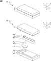
- FIG. 2A is a perspective view of the acceleration detection device according to the first embodiment of the present invention
- FIG. 2B is an exploded perspective view of the acceleration detection device according to the first embodiment
- FIG. 3A to FIG. 3D are perspective views for explaining an example of a method for manufacturing the acceleration detection device according to the first embodiment.
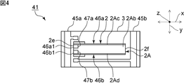
- FIG. 4 is a plan view of the acceleration detection device according to the first modification of the first embodiment of the present invention, in which the second package member is omitted.
- FIG. 5A is a plan view of the acceleration detection device according to the second modification of the first embodiment of the present invention, in which the second package member is omitted
- FIG. FIG. 6 is a cross-sectional view of the acceleration detection device along the line BB in FIG. 5A, with the second package member omitted.
- FIG. 6A is a plan view of the acceleration detection device according to the third modification of the first embodiment of the present invention, in which the second package member is omitted, and FIG. These are sectional drawings of the acceleration detection apparatus which abbreviate
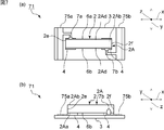
- FIG. 7A is a plan view of the acceleration detection device according to the fourth modification of the first embodiment of the present invention, in which the second package member is omitted, and FIG. These are the figures of the acceleration detection apparatus which abbreviate
- FIG. 8 is a plan view of the acceleration detection device according to the fifth modification of the first embodiment of the present invention, in which the second package member is omitted.
- FIG. 9A is a plan view of the acceleration detection device according to the second embodiment of the present invention, in which the second package member is omitted, and FIG. 9B is the second embodiment.
- FIG. 9C is a view of the acceleration detection device in which the second package member is omitted as viewed from the first side surface of the piezoelectric body in the embodiment, and FIG. 9C is a second side surface of the piezoelectric body in the second embodiment. It is the figure of the acceleration detection apparatus which abbreviate
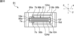
- FIG. 10 is a top view of the acceleration detection apparatus which abbreviate
- FIG. 11A is a plan view of an acceleration detection device in which the second package member is omitted
- FIG. 11B is a third embodiment of the acceleration detection device according to the third embodiment of the present invention.
- FIG. 11C is a view of the acceleration detection device in which the second package member is omitted, as viewed from the first side surface of the piezoelectric body in the embodiment, and FIG. 11C is a second side surface of the piezoelectric body in the third embodiment.
- FIG. 11A is a plan view of an acceleration detection device in which the second package member is omitted
- FIG. 11B is a third embodiment of the acceleration detection device according to the third embodiment of the present invention.
- FIG. 11C is a view of the acceleration detection device in which the second package member is omitted, as viewed from the
- FIG. 11D is a view of the acceleration detection device from which the second package member is omitted as viewed from the side, and FIG. 11D is a second package of the acceleration detection device along the line DD in FIG. It is sectional drawing of the acceleration detection apparatus which abbreviate
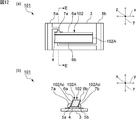
- FIG. 12A is a plan view of an acceleration detection device according to a seventh modification of the first embodiment of the present invention, in which the second package member is omitted
- FIG. FIG. 13 is a cross-sectional view of the acceleration detection device along the line EE in FIG. 12A, with the second package member omitted.
- FIG. 13A is a plan view of an acceleration detection device according to an eighth modification of the third embodiment of the present invention, and FIG.
- FIG. 13B shows an acceleration detection device according to the eighth modification.
- FIG. 13C is a plan view of the acceleration detection device in which the second package member is omitted, and FIG. 13C is an illustration of the second package member as viewed from the first side surface of the piezoelectric body in the eighth modification.
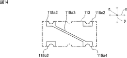
- FIG. FIG. 14 is a schematic plan view showing an electrode structure on the lower surface of the first package member in the eighth modification example of the third embodiment of the present invention.
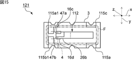
- FIG. 15: is the top view which abbreviate
- FIG. 16 is a side sectional view of an acceleration detection device according to the fourth embodiment of the present invention.
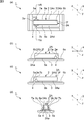
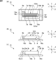
- FIG. 1A is a plan view of an acceleration detection device according to the first embodiment of the present invention.
- FIG. 1B is a diagram of the acceleration detection device viewed from the first side surface side of the piezoelectric body according to the first embodiment.
- FIG.1 (c) is a figure of the acceleration detection apparatus seen from the 2nd side surface side of the piezoelectric material in 1st Embodiment.
- FIG. 1D is a cross-sectional view of the acceleration detecting device along the line AA in FIG. In FIGS. 1A to 1D, a second package member to be described later is omitted.
- the acceleration detection device 1 has a first package member 3.
- the first package member 3 has a flat shape.
- the 1st package member 3 is not specifically limited, For example, it consists of glass epoxy resin. Or you may consist of appropriate ceramics.
- First and second wirings 5a and 5b are provided on the first package member 3. Further, a sheet-like adhesive 4 is provided on the first package member 3. As shown in FIGS. 1B and 1C, the piezoelectric element 2 is bonded onto the first package member 3 by a sheet-like adhesive 4.
- the sheet-like adhesive 4 is made of an insulating material such as an epoxy resin. In addition, the material of the sheet-like adhesive 4 is not specifically limited.
- the piezoelectric element 2 has a piezoelectric body 2A and first and second electrodes 6a and 6b.
- the piezoelectric body 2A has a rectangular parallelepiped shape and has a length direction.
- the piezoelectric body 2A has a lower surface 2Aa and an upper surface 2Ab extending in the length direction.
- the piezoelectric body 2A has a first side surface 2Ac extending in the length direction and a second side surface 2Ad facing the first side surface 2Ac.
- the piezoelectric body 2A is made of, for example, a piezoelectric single crystal or piezoelectric ceramics.
- the piezoelectric body 2A is a single layer piezoelectric body.
- the piezoelectric element 2 may have a plurality of piezoelectric layers.
- the first electrode 6a is provided on the first side surface 2Ac of the piezoelectric body 2A.
- the second electrode 6b is provided on the second side surface 2Ad of the piezoelectric body 2A.
- the piezoelectric element 2 is bonded onto the first package member 3 by a sheet-like adhesive 4 provided on the lower surface 2Aa of the piezoelectric element 2. That is, the piezoelectric element 2 is bonded onto the first package member 3 from the lower surface 2Aa side of the piezoelectric body 2A.
- the piezoelectric element 2 has a first end 2e, which is one end in the length direction.
- the piezoelectric element 2 also has a second end 2f that faces the first end 2e.
- the piezoelectric element 2 is supported by a cantilever with a sheet-like adhesive 4 on the first end 2e side.
- the second end 2 f is a free end of the piezoelectric element 2.
- the sheet-like adhesive 4 reaches the first end 2e. Note that the sheet-like adhesive 4 may not reach the first end 2e.
- the first electrode 6a is electrically connected to the first wiring 5a by a conductive adhesive 7a.
- the second electrode 6b is also electrically connected to the second wiring 5b by the conductive adhesive 7b.
- the piezoelectric element 2 is electrically connected to the outside.
- the conductive adhesives 7 a and 7 b are provided at positions overlapping the sheet-like adhesive 4 in a plan view from the upper surface 2 Ab side of the piezoelectric element 2.
- the position where the first and second electrodes 6a and 6b and the first and second wirings 5a and 5b are connected by the conductive adhesives 7a and 7b is not particularly limited. Although it does not specifically limit as conductive adhesive 7a, 7b, For example, the Si type adhesive agent containing a conductor, etc. can be used.
- the length direction of the piezoelectric element 2 is defined as the x direction.
- the direction perpendicular to the length direction of the piezoelectric element 2 is defined as the y direction.
- the direction perpendicular to the xy plane is taken as the z direction.
- the surface of the first package member 3 to which the piezoelectric element 2 is bonded is parallel to the xy plane.
- the first and second electrodes 6a and 6b face each other in the y direction. That is, the principal axis direction of the acceleration detecting device 1 is 0 ° with respect to the xy plane.
- FIG. 2 (a) is a perspective view of the acceleration detecting device according to the first embodiment of the present invention.
- FIG. 2B is an exploded perspective view of the acceleration detection device according to the first embodiment.
- the acceleration detecting device 1 has a second package member 8 joined to the first package member 3.
- the second package member 8 has a cap shape.
- the piezoelectric element 2 is sealed by the first package member 3 and the second package member 8.
- the acceleration detection device 1 does not necessarily have the second package member 8.
- the piezoelectric element 2 is preferably sealed by the first package member 3 and the second package member 8. Thereby, the strength of the acceleration detecting device 1 can be increased and it is difficult to be affected by external mechanical noise.
- the second package member is made of metal, and this potential is dropped to the ground, so that it is hardly affected by electromagnetic noise.
- the material of the 2nd package member 8 is not specifically limited, For example, you may consist of ceramics.
- the feature of the acceleration detection device 1 of the present embodiment is that the piezoelectric element 2 is bonded onto the first package member 3 by a sheet-like adhesive 4. As a result, the acceleration detection device 1 is less likely to cause a shift in the position and holding angle of the piezoelectric element and is less susceptible to noise. This will be described below.
- the piezoelectric element in an acceleration detection device in which a piezoelectric element is supported by an adhesive, the piezoelectric element has not been sufficiently fixed before the adhesive is cured. For this reason, the holding angle of the piezoelectric element is easily shifted due to the influence of gravity or the like. Further, when the adhesive is cured, the adhesive expands or contracts, and thus the holding angle and position of the piezoelectric element may be shifted.
- the piezoelectric element 2 is supported by a sheet-like adhesive 4.
- the sheet-like adhesive 4 supports the piezoelectric element 2 on the surface. Therefore, the posture of the piezoelectric element 2 can be stabilized. Therefore, it is possible to effectively suppress the shift of the holding angle.
- the piezoelectric element 2 is bonded onto the first package member 3 via a sheet-like adhesive 4. Therefore, the piezoelectric element 2 is not in direct contact with the first package member 3. Furthermore, the piezoelectric element 2 is supported at one place by a sheet-like adhesive 4. Therefore, it is difficult to be affected by noise due to the deflection of the first package member 3 or the like.
- the first and second electrodes 6a and 6b are provided on the first and second side surfaces 2Ac and 2Ad of the piezoelectric body 2A.
- the first and second electrodes 6a and 6b are electrically connected to the first and second wirings 5a and 5b by conductive adhesives 7a and 7b.
- the conductive adhesives 7a and 7b are provided to electrically connect the first and second electrodes 6a and 6b and the first and second wirings 5a and 5b.
- the connection is not strong. That is, it hardly contributes to the support of the piezoelectric element 2. Therefore, the influence of noise due to the deflection of the first package member 3 can be effectively suppressed.
- the piezoelectric element 2 is supported by a cantilever beam.
- the sheet-like adhesive 4 reaches the first end 2 e of the piezoelectric element 2. Thereby, the distance between the portion where the piezoelectric element 2 is supported and the second end 2f which is a free end can be increased. Therefore, the sensitivity of the acceleration detection device 1 can be effectively increased.
- the first and second electrodes 6a and 6b are provided on the first and second side surfaces 2Ac and 2Ad of the piezoelectric body 2A, and are exposed to the outside. Therefore, it can be easily electrically connected to the outside. Furthermore, since the sheet-like adhesive 4 is made of an insulator, the first electrode 6a and the second electrode 6b can be electrically and reliably insulated.
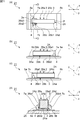
- 3 (a) to 3 (d) are perspective views for explaining an example of a method for manufacturing the acceleration detection device according to the first embodiment.
- a piezoelectric element 2 having a piezoelectric body 2A is prepared.
- a sheet-like adhesive 4 is attached on the lower surface of the piezoelectric element 2.
- a semi-cured sheet-like adhesive 4 is attached so as to reach the first end 2 e of the piezoelectric element 2.
- the piezoelectric element 2 is joined to the first package member 3 by the sheet-like adhesive 4. Since the piezoelectric element 2 can be supported on the surface by the sheet-like adhesive 4, the posture of the piezoelectric element 2 can be stabilized. Therefore, it is possible to effectively suppress the shift of the holding angle.
- the sheet-like adhesive 4 is in a semi-cured state during the above-described joining. Therefore, the shape of the sheet-like adhesive 4 hardly changes during curing. Therefore, it is difficult for the position of the piezoelectric element 2 and the holding angle to shift.
- first and second electrodes 6a and 6b are provided on the first and second side surfaces 2Ac and 2Ad of the piezoelectric body 2A.
- first and second wirings 5a and 5b are provided on the first package member 3.
- the second electrode 6b and the second wiring 5b are electrically connected by the conductive adhesive 7b.
- the first electrode 6a and the first wiring 5a are electrically connected by a conductive adhesive.
- the piezoelectric element is sealed by bonding the second package member 8 onto the first package member 3. Thereby, the acceleration detection apparatus 1 can be obtained.
- the form of electrical connection between the first and second electrodes 6a and 6b and the first and second wirings 5a and 5b is not particularly limited. Even if the form of the connection is another form, as in the first embodiment, the position of the piezoelectric element 2 and the displacement of the holding angle are unlikely to occur. This will be described using the following first to third modifications as examples.
- the first and second electrodes 46a and 46b and the first and second wirings 45a and 45b are electrically connected by bonding wires 47a and 47b. It may be connected to. More specifically, the first electrode 46a includes a first extraction electrode 46a1 that is extracted on the upper surface 2Ab of the piezoelectric body 2A. The second electrode 46b also includes a second extraction electrode 46b1 that is extracted on the upper surface 2Ab of the piezoelectric body 2A. The first lead electrode 46a1 and the first wiring 45a are electrically connected by a bonding wire 47a. The second lead electrode 46b1 and the second wiring 45b are electrically connected by a bonding wire 47b.
- FIG. 5A is a plan view of an acceleration detection device according to a second modification of the first embodiment.
- FIG. 5B is a cross-sectional view of the acceleration detecting device along the line BB in FIG. Note that the second package member is omitted in the drawings other than FIGS. 2 and 3 and FIGS. 13A and 14 described below.
- the first electrode 46a of the acceleration detecting device 51 has a first extraction electrode 46a1 that is extracted on the lower surface 2Aa of the piezoelectric body 2A.
- the second electrode 46b also includes a second extraction electrode 46b1 that is extracted on the lower surface 2Aa of the piezoelectric body 2A.
- the first wiring 55a is routed to a position overlapping the first extraction electrode 46a1 in a plan view from the upper surface 2Ab side of the piezoelectric body 2. Yes.
- the second wiring 55b is also routed to a position overlapping the second extraction electrode 46b1 in plan view.
- the first and second lead electrodes 46a1 and 46b1 and the first and second wirings 55a and 55b are joined by a sheet-like adhesive 54.
- the sheet-like adhesive 54 of the second modified example has anisotropic conductivity. More specifically, the sheet-like adhesive 54 has conductivity only in the thickness direction, that is, the z direction. Therefore, the first extraction electrode 46a1 and the first wiring 55a are electrically connected. The second extraction electrode 46b1 and the second wiring 55b are electrically connected.
- the sheet-like adhesive 54 does not have conductivity in the direction parallel to the xy plane. Therefore, the first extraction electrode 46a1 and the first wiring 55a are not electrically connected to the second extraction electrode 46b1 and the second wiring 55b.
- the sheet-like adhesive 54 may have a conductor penetrating in the thickness direction, for example. Thereby, the anisotropic conductivity can be obtained.
- the piezoelectric element 2 and the first package member 3 are joined at one location by a sheet-like adhesive 54. Therefore, it is difficult to be affected by noise due to the deflection of the first package member 3 or the like.
- FIG. 6A is a plan view of an acceleration detection device according to a third modification of the first embodiment.
- FIG. 6B is a cross-sectional view of the acceleration detecting device taken along the line CC in FIG.
- the acceleration detection device 61 includes first and second lead electrodes 46a1 and 46b1 as in the second modification. As shown in FIGS. 6A and 6B, the first extraction electrode 46a1 and the first wiring 55a are electrically connected by a bump 67a. The second lead electrode 46b1 and the second wiring 55b are electrically connected by a bump 67b.
- a sheet-like adhesive 64 is provided on a portion of the lower surface 2Aa of the piezoelectric body 2 where the first and second lead electrodes 46a1 and 46b1 are not provided.
- the sheet-like adhesive 4 reaches the first end 2e of the piezoelectric element 2. As described above, the sheet-like adhesive 4 does not necessarily have to reach the first end 2e.
- the distance between the portion where the piezoelectric element 2 is supported and the second end 2 f which is a free end can be adjusted. Thereby, the sensitivity of the acceleration detection apparatus 1 can be adjusted.
- the present invention can also be suitably applied to acceleration detection devices other than supporting a piezoelectric element with a cantilever beam.
- the piezoelectric element 2 may be supported at both ends in the length direction as in the acceleration detection device 71 of the fourth modification shown in FIGS. 7A and 7B.
- the acceleration detection device 71 has a sheet-like adhesive 4 that reaches the first end 2e.
- the acceleration detection device 71 also includes a sheet-like adhesive 4 that reaches the second end 2f.
- the piezoelectric element 2 is supported at both ends by a sheet-like adhesive 4 provided at two locations. Note that the sheet-like adhesive 4 does not necessarily reach the first and second ends 2e and 2f of the piezoelectric element 2.
- the first electrode 6a is connected to the first wiring 75a by the conductive adhesive 7a at a position overlapping the sheet-like adhesive 4 in a plan view from the upper surface 2Ab side of the piezoelectric element 2.
- the second electrode 6b is connected to the second wiring 75b by the conductive adhesive 7b at a position overlapping the sheet-like adhesive 4 in plan view.
- the first and second electrodes 6a and 6b and the first and second wirings 75a and 75b are electrically connected.
- the position of the piezoelectric element 2 and the holding angle are not easily displaced and are not easily affected by noise.
- the piezoelectric element 2 may be supported by the sheet-like adhesive 4 in the length direction, that is, in the vicinity of the center in the x direction, like the acceleration detection device 81 of the fifth modification shown in FIG. Even in this case, the same effect as the first embodiment can be obtained.
- FIG. 9A is a plan view of the acceleration detection device according to the second embodiment of the present invention.
- FIG. 9B is a diagram of the acceleration detection device viewed from the first side surface side of the piezoelectric body according to the second embodiment.
- FIG. 9C is a diagram of the acceleration detection device viewed from the second side surface of the piezoelectric body according to the second embodiment.
- the acceleration detecting device 11 is provided inside the piezoelectric element 12, and has a plurality of first and second internal electrodes 19a, 19b facing each other.
- the piezoelectric element 12 is composed of a laminate of piezoelectric materials. Except for the above, the acceleration detection device 11 has the same configuration as the acceleration detection device 1 of the first embodiment. Note that it is sufficient that at least one of the first and second internal electrodes 19a and 19b is provided.
- the plurality of first and second internal electrodes 19a and 19b are also opposed to the first and second electrodes 16a and 16b.
- the plurality of first internal electrodes 19 a and the first electrode 16 a are led out to the first end 12 e of the piezoelectric element 12.
- a first connection electrode 16c is provided on the first end 12e.
- the plurality of first internal electrodes 19a and the first electrode 16a are electrically connected by a first connection electrode 16c.
- a plurality of second internal electrodes 19b and second electrodes 16b are also drawn out to the second end 12f.
- a second connection electrode 16d is provided on the second end 12f.
- the plurality of second internal electrodes 19b and the second electrode 16b are electrically connected by a second connection electrode 16d.
- the acceleration detecting device 11 since the acceleration detecting device 11 includes the first and second internal electrodes 19a and 19b, the capacitance is large. Moreover, the sensitivity can be effectively increased.
- the piezoelectric element 12 is supported by the sheet-like adhesive 4 as in the first embodiment. Accordingly, the position of the piezoelectric element 12 and the holding angle are not easily displaced and are not easily affected by noise.
- the total number of the first and second internal electrodes 19a and 19b is an even number.
- the number of layers of the piezoelectric element 12 is an odd number.
- the total number of the first and second internal electrodes 19 a and 19 b is an odd number, and the number of layers of the piezoelectric elements 12 is May be an even number.
- the form of electrode connection is different from that of the second embodiment. More specifically, the first electrode 96 a is provided on the first end 12 e of the piezoelectric element 12. The first internal electrode 19a reaches the first end 12e, and is physically and electrically connected to the first electrode 96a.
- the second electrode 96b is provided on the first and second side surfaces 12Ac and 12Ad of the piezoelectric body 12A.
- a connection electrode 16 d is provided on the second end portion 12 f of the piezoelectric element 12.
- the second electrodes 96b are connected by a connection electrode 16d.
- the second internal electrode 19b is also electrically connected to the second electrode 96b through the connection electrode 16d.
- the first wiring 95a is electrically connected to the first electrode 96a by the conductive adhesive 7a.
- the second wiring 95b extends toward the first and second side surfaces 12Ac and 12Ad of the piezoelectric body 12, respectively.
- the second wiring 95b is connected to the second electrode 96b on the first and second side faces 12Ac and 12Ad by the conductive adhesive 7b.
- the conductive adhesive 7b may be one place. Accordingly, the second wiring 95b is electrically connected to the second electrode 96b.
- the capacitance of the acceleration detection device 91 is large as in the second embodiment. Therefore, the sensitivity can be effectively increased. Further, the position of the piezoelectric element 12 and the holding angle are not easily displaced and are not easily affected by noise.
- the piezoelectric element 12 is a laminated body.
- the first and second internal electrodes 19a and 19b may be embedded in a piezoelectric element made of a single layer piezoelectric body.
- FIG. 11 (a) is a plan view of an acceleration detection device according to the third embodiment of the present invention.
- FIG. 11B is a diagram of the acceleration detection device viewed from the first side surface of the piezoelectric body according to the third embodiment.
- FIG. 11C is a diagram of the acceleration detection device viewed from the second side surface of the piezoelectric body according to the third embodiment.
- FIG. 11D is a cross-sectional view of the acceleration detecting device along the line DD in FIG.
- the first electrode 26a is provided on the upper surface 2Ab of the piezoelectric body 2.
- the second electrode 26b is provided on the lower surface 2Aa of the piezoelectric body 2A.
- the acceleration detection device 21 has the same configuration as the acceleration detection device 1 of the first embodiment.
- the first electrode 26a has a first extraction electrode 26a1 that is extracted on the first side surface 2Ac of the piezoelectric body 2A.
- the first lead electrode 26a1 is electrically connected to the first wiring 5a by the conductive adhesive 7a.
- the second electrode 26b also includes a second extraction electrode 26b1 that is extracted on the second side surface 2Ad of the piezoelectric body 2A.
- the second lead electrode 26b1 is electrically connected to the second wiring 5b by the conductive adhesive 7b.
- the first electrode 26a is provided with a notch 26a2. Thereby, a gap is arranged between the first electrode 26a and the second extraction electrode 26b1.
- the second electrode 26b is also provided with a notch 26b2. Thereby, a gap is arranged between the second electrode 26b and the first extraction electrode 26a. Therefore, the first electrode 26a and the second electrode 26b are not electrically connected.
- the first electrode 26a and the second electrode 26b may not be electrically connected, and the first and second cutout portions 26a2 and 26b2 are not necessarily provided.
- the first extraction electrode 26a1 may be provided so as not to reach the end portion on the lower surface 2Aa side of the first side surface 2Ac of the piezoelectric body 2A.
- the second extraction electrode 26b1 may also be provided so as not to reach the end portion on the upper surface 2Ab side of the second side surface 2Ad of the piezoelectric body 2A.
- the first and second electrodes 26a and 26b are opposed to each other in the z direction. That is, the principal axis direction of the acceleration detection device 21 is 90 ° with respect to the xy plane.
- the main axis direction of the acceleration detection device of the present invention is not limited to 0 ° or 90 ° with respect to the xy plane. This example is shown by the 7th modification of the following 1st Embodiment.
- FIG. 12 (a) is a plan view of an acceleration detection device according to a seventh modification.
- FIG. 12B is a cross-sectional view of the acceleration detection device taken along line EE in FIG.
- the first and second side surfaces 102Ac and 102Ad of the piezoelectric body 102A in the piezoelectric element 102 are inclined with respect to the z direction. Therefore, the first and second electrodes 6a and 6b are opposed to each other in the direction inclined from the y direction and the z direction.
- the principal axis direction of the acceleration detection device 101 is a direction inclined by 25 ° with respect to the xy plane on the yz plane.
- the main axis direction of the acceleration detection device 101 is not particularly limited.
- FIG. 13A is a plan view of an acceleration detection device according to an eighth modification of the third embodiment.
- FIG. 13B is a plan view of the acceleration detection device according to the eighth modification, in which the second package member is omitted.
- FIG. 13C is a view of the acceleration detection device in which the second package member is omitted, as viewed from the first side surface of the piezoelectric body according to the eighth modification.
- the dashed-dotted line F of FIG.13 (b) shows the part to which the 2nd package member is joined.
- the acceleration detection device 111 may have a ground wiring 115c1 on the upper surface of the first package member 113.
- the ground wiring 115c1 is electrically connected to the second package member 8 via a conductive adhesive.
- FIG. 14 is a schematic plan view showing the electrode structure on the lower surface of the first package member 113.
- a ground terminal 115 c 2 is provided on the lower surface of the first package member 113.
- the ground wiring 115c1 is connected to the ground terminal 115c2 on the lower surface through the side surface from the upper surface of the first package member 113.
- the second package member 8 is connected to the ground potential via the ground wiring 115c1 and the ground terminal 115c2. In this case, it is much less susceptible to electromagnetic noise.
- the second package member 8 is not particularly limited, but may be joined to the first package member 113 by an insulating adhesive other than a portion in contact with the ground wiring 115c1.
- the first and second wirings 115a1 and 1152 connected to the first and second connection electrodes 16c and 16d of the piezoelectric element 112 are formed on the upper surface of the first package member 113.
- 115b1 is provided on the upper surface of the first package member 113.
- a third wiring 115 a 5 is provided on the upper surface of the first package member 113.
- first, second and third terminal electrodes 115a2, 115b2, 115a4 and a third connection electrode 115a3 are provided on the lower surface of the first package member 113.
- the first terminal electrode 115a2 and the third terminal electrode 115a4 are connected to the third connection electrode 115a3.
- the first, second, and third wirings 115a1, 115b1, and 115a5 shown in FIG. 13A pass from the upper surface of the first package member 113 to the side surface, and then the first, second, and third terminal electrodes 115a2. , 115b2 and 115a4.
- the first wiring 115a1 is electrically connected to the third wiring 115a5 through the first terminal electrode 115a2, the third connection electrode 115a3, and the third terminal electrode 115a4.
- the piezoelectric element 112 has a plurality of first and second internal electrodes 119a and 119b facing each other in the thickness direction.
- the stacking direction of the plurality of internal electrodes 119a and 119b may be the thickness direction of the piezoelectric element 112.
- the first package member 113 may be open on the side surface side and may have a plurality of recesses provided continuously in the thickness direction. .
- first, second and third wirings 115a1, 115b1, 115a5 and a ground wiring 115c1 are provided.
- the first connection wiring 16c may be connected to the first wiring 115a1 by a bonding wire 47a.
- the second electrode 26b may be connected to the second wiring 115b1 by a bonding wire 47b.
- FIG. 16 is a side cross-sectional view of an acceleration detection apparatus according to the fourth embodiment of the present invention.
- the first package member 33 of the acceleration detection device 31 has a recess 33a.
- the second package member 38 has a flat plate shape. Except for the above points, the acceleration detection device 31 has the same configuration as the acceleration detection device 1 of the first embodiment.
- the piezoelectric element 2 is located in the recess 33 a of the first package member 33.
- the second package member 38 is joined to the first package member 33 so as to cover the recess 33a.
- the shape of the second package member 38 is not particularly limited as long as it can be joined so as to cover the recess 33a.
- the position of the piezoelectric element 2 and the holding angle are not easily displaced and are not easily affected by noise.
Landscapes
- Physics & Mathematics (AREA)
- General Physics & Mathematics (AREA)
- Pressure Sensors (AREA)
- Force Measurement Appropriate To Specific Purposes (AREA)
Abstract
圧電素子の位置や保持角度のずれが生じ難く、かつノイズの影響を受け難い、加速度検出装置及びその製造方法を提供する。 加速度検出装置1は、上面及び下面を有する圧電素子2と、圧電素子2の下面上に設けられているシート状の接着剤4と、シート状の接着剤4により圧電素子2が接合されている第1のパッケージ部材3とを備える。
Description
本発明は、パッケージ部材に固定されている加速度検出装置及びその製造方法に関する。
下記の特許文献1には、加速度検出装置の一例が開示されている。この加速度検出装置においては、圧電素子が支持枠に挟まれることにより、保持されている。
下記の特許文献2に記載の加速度検出装置においても、圧電素子はケース部材に挟まれることにより保持されている。
下記の特許文献3では、圧電素子が瞬間接着剤及び導電性接着剤により、ベース部材に固定されている。
下記の特許文献4では、圧電素子がケース部材の素子取り付け部に挟まれている。さらに、圧電素子は、導電性接着剤及び絶縁性接着剤により固定されている。
特許文献1及び2における加速度検出装置では、圧電素子が支持枠またはケース部材により直接挟まれることにより強固に保持されていた。そのため、支持枠やケース部材のたわみなどにより生じるノイズの影響を強く受けやすかった。
特許文献3における加速度検出装置では、瞬間接着剤及び導電性接着剤の硬化前に、圧電素子にかかる重力の影響により、圧電素子の位置及び保持角度がずれやすかった。さらに、瞬間接着剤及び導電性接着剤は、硬化するに際して大きく膨張または収縮する。それによっても、圧電素子の位置及び保持角度がずれやすかった。
特許文献4における加速度検出装置においても、導電性接着剤及び絶縁性接着剤が硬化するに際しての膨張または収縮により、圧電素子の位置及び保持角度がずれやすかった。さらに、圧電素子が素子取り付け部に挟まれているため、ケース部材のたわみなどにより生じるノイズの影響を受けやすかった。
本発明の目的は、圧電素子の位置や保持角度のずれが生じ難く、かつノイズの影響を受け難い、加速度検出装置及びその製造方法を提供することにある。
本発明に係る加速度検出装置は、上面及び下面を有する圧電素子と、前記圧電素子の前記下面上に設けられているシート状の接着剤と、前記シート状の接着剤により前記圧電素子が接合されている第1のパッケージ部材とを備える。
本発明に係る加速度検出装置のある特定の局面では、前記圧電素子が、圧電体と、前記圧電体上に設けられている第1,第2の電極とを有し、前記圧電体が、上面及び下面と、第1の側面及び該第1の側面に対向している第2の側面とを有する。この場合には、外部と電気的に容易に接続することができる。
本発明に係る加速度検出装置の他の特定の局面では、前記第1の電極が前記圧電体の前記第1の側面上に設けられており、前記第2の電極が前記圧電体の前記第2の側面上に設けられている。この場合には、外部と電気的に容易に接続することができる。
本発明に係る加速度検出装置のさらに他の特定の局面では、前記第1の電極が前記圧電体の前記下面上に設けられており、前記第2の電極が前記圧電体の前記上面上に設けられている。この場合には、外部と電気的に容易に接続することができる。
本発明に係る加速度検出装置の別の特定の局面では、前記圧電素子が、前記第1の電極に接続されており、前記圧電体の前記第1の側面に設けられている第1の引き出し電極と、前記第2の電極に接続されており、前記圧電体の前記第2の側面に設けられている第2の引き出し電極とを有する。この場合には、外部と電気的に容易に接続することができる。
本発明に係る加速度検出装置のさらに別の特定の局面では、前記圧電素子が長さ方向を有し、前記上面及び下面が前記長さ方向に延びており、前記圧電素子が少なくとも1箇所の自由端を有するように、前記シート状の接着剤により固定されている。この場合には、圧電素子の位置や保持角度のずれがより一層生じ難く、ノイズの影響をより一層受け難い。
本発明に係る加速度検出装置のさらに別の特定の局面では、前記圧電素子が、前記シート状の接着剤により片持ち梁で支持されている。この場合には、圧電素子の位置や保持角度のずれがより一層生じ難く、かつノイズの影響をより一層受け難い。
本発明に係る加速度検出装置のさらに別の特定の局面では、前記シート状の接着剤が、前記圧電素子の前記長さ方向の端部の内の一方に至っている。この場合には、感度を効果的に高めることができる。
本発明に係る加速度検出装置のさらに別の特定の局面では、前記圧電素子の内部に設けられており、互いに対向し合っている第1,第2の内部電極がさらに備えられている。この場合には、静電容量が大きい。また、感度を効果的に高めることができる。
本発明に係る加速度検出装置のさらに別の特定の局面では、前記シート状の接着剤が絶縁性の材料からなる。この場合には、第1の電極と第2の電極とを電気的に確実に絶縁することができる。
本発明に係る加速度検出装置のさらに別の特定の局面では、前記第1のパッケージ部材に接合されている第2のパッケージ部材がさらに備えられており、前記第1,第2のパッケージ部材により前記圧電素子が封止されている。この場合には、強度を高めることができ、かつ外部からのノイズの影響を受け難い。
本発明に係る加速度検出装置のさらに別の特定の局面では、前記第1のパッケージ部材が平板状であり、前記第2のパッケージ部材がキャップ状である。この場合には、強度を高めることができ、かつ外部からのノイズの影響を受け難い。
本発明に係る加速度検出装置のさらに別の特定の局面では、前記第1のパッケージ部材が凹部を有し、前記圧電素子が前記凹部内に配置されており、前記第2のパッケージ部材が前記凹部を覆うように設けられていることにより、前記圧電素子が封止されている。この場合には、強度を高めることができ、かつ外部からのノイズの影響を受け難い。
本発明に係る加速度検出装置の製造方法は、本発明に従い構成されている加速度検出装置の製造方法であって、前記圧電素子を用意する工程と、前記圧電素子の前記下面上に前記シート状の接着剤を貼り付ける工程と、前記圧電素子を、前記シート状の接着剤を介して前記第1のパッケージ部材上に接合する工程とを備える。この場合には、圧電素子の位置や保持角度のずれがより一層生じ難く、かつノイズの影響を受け難い加速度検出装置を得ることができる。
本発明によれば、圧電素子の位置や保持角度のずれが生じ難く、かつノイズの影響を受け難い、加速度検出装置及びその製造方法を提供することができる。
以下、図面を参照しつつ、本発明の具体的な実施形態を説明することにより、本発明を明らかにする。
なお、本明細書に記載の各実施形態は、例示的なものであり、異なる実施形態間において、構成の部分的な置換または組み合わせが可能であることを指摘しておく。
図1(a)は、本発明の第1の実施形態に係る加速度検出装置の平面図である。図1(b)は、第1の実施形態における圧電体の第1の側面側から見た加速度検出装置の図である。図1(c)は、第1の実施形態における圧電体の第2の側面側から見た加速度検出装置の図である。図1(d)は、図1(a)中のA-A線に沿う加速度検出装置の断面図である。なお、図1(a)~図1(d)では、後述する第2のパッケージ部材を省略している。
図1(a)に示すように、加速度検出装置1は、第1のパッケージ部材3を有する。第1のパッケージ部材3は、平板状の形状を有する。第1のパッケージ部材3は、特に限定されないが、例えば、ガラスエポキシ樹脂からなる。あるいは、適宜のセラミックスからなっていてもよい。
第1のパッケージ部材3上には、第1,第2の配線5a,5bが設けられている。さらに、第1のパッケージ部材3上には、シート状の接着剤4が設けられている。図1(b)及び図1(c)に示すように、シート状の接着剤4により、第1のパッケージ部材3上に、圧電素子2が接合されている。シート状の接着剤4は、エポキシ樹脂などの絶縁性の材料からなる。なお、シート状の接着剤4の材料は、特に限定されない。
図1(a)及び図1(d)に示すように、圧電素子2は、圧電体2A及び第1,第2の電極6a,6bを有する。圧電体2Aは直方体状であり、長さ方向を有する。圧電体2Aは、長さ方向に延びる下面2Aa及び上面2Abを有する。さらに、圧電体2Aは、長さ方向に延びる第1の側面2Ac及び第1の側面2Acに対向している第2の側面2Adを有する。圧電体2Aは、例えば、圧電単結晶や圧電セラミックスなどからなる。本実施形態では、圧電体2Aは単層の圧電体である。なお、圧電素子2は、複数の圧電体層を有してもよい。
第1の電極6aは、圧電体2Aの第1の側面2Ac上に設けられている。第2の電極6bは、圧電体2Aの第2の側面2Ad上に設けられている。
圧電素子2は、圧電素子2の下面2Aa上に設けられているシート状の接着剤4により、第1のパッケージ部材3上に接合されている。すなわち、圧電体2Aの下面2Aa側から、圧電素子2は第1のパッケージ部材3上に接合されている。
図1(a)及び図1(b)に示すように、圧電素子2は、長さ方向の一方の端部である、第1の端部2eを有する。圧電素子2は、第1の端部2eに対向している第2の端部2fも有する。圧電素子2は、第1の端部2e側において、シート状の接着剤4により、片持ち梁で支持されている。第2の端部2fは、圧電素子2の自由端である。シート状の接着剤4は、第1の端部2eに至っている。なお、シート状の接着剤4は、第1の端部2eに至っていなくてもよい。
図1(a)及び図1(d)に示すように、第1の電極6aは、導電性接着剤7aにより第1の配線5aに電気的に接続されている。第2の電極6bも、導電性接着剤7bにより第2の配線5bに電気的に接続されている。それによって、圧電素子2は、外部に電気的に接続されている。
導電性接着剤7a,7bは、圧電素子2の上面2Ab側からの平面視において、シート状の接着剤4と重なる位置に設けられている。なお、導電性接着剤7a,7bにより、第1,第2の電極6a,6bと第1,第2の配線5a,5bとを接続する位置は、特に限定されない。導電性接着剤7a,7bとしては、特に限定されないが、例えば、導電体を含むSi系の接着剤などを用いることができる。
図1(a)~図1(d)に示すように、圧電素子2の長さ方向をx方向とする。圧電素子2の長さ方向に垂直な方向をy方向とする。x-y平面に垂直な方向をz方向とする。ここで、圧電素子2が接合されている第1のパッケージ部材3の面はx-y平面に平行である。第1,第2の電極6a,6bは、y方向において対向し合っている。すなわち、加速度検出装置1の主軸方向は、x-y平面に対して0°である。
図2(a)は、本発明の第1の実施形態に係る加速度検出装置の斜視図である。図2(b)は、第1の実施形態に係る加速度検出装置の分解斜視図である。
図2(a)に示すように、加速度検出装置1は、第1のパッケージ部材3上に接合されている第2のパッケージ部材8を有する。第2のパッケージ部材8は、キャップ状の形状を有する。図2(a)及び図2(b)に示すように、第1のパッケージ部材3及び第2のパッケージ部材8により、圧電素子2が封止されている。
加速度検出装置1は、第2のパッケージ部材8を必ずしも有しなくともよい。もっとも、圧電素子2は、第1のパッケージ部材3及び第2のパッケージ部材8により封止されていることが好ましい。それによって、加速度検出装置1の強度を高めることができ、かつ外部からの機械的ノイズの影響を受け難い。また、第2のパッケージ部材を金属で構成し、この電位をグラウンドに落とすことにより、電磁ノイズの影響も受け難い。なお、第2のパッケージ部材8の材料は特に限定されず、例えば、セラミックスからなっていてもよい。
本実施形態の加速度検出装置1の特徴は、圧電素子2がシート状の接着剤4により第1のパッケージ部材3上に接合されていることにある。これにより、加速度検出装置1は、圧電素子の位置や保持角度のずれが生じ難く、かつノイズの影響を受け難い。これを、以下において説明する。
従来、接着剤により圧電素子が支持されている加速度検出装置では、接着剤を硬化させる前においては、圧電素子が充分に固定されていなかった。そのため、重力などの影響により、圧電素子の保持角度がずれ易かった。さらに、接着剤が硬化するに際し、接着剤が膨張または収縮するため、圧電素子の保持角度及び位置がずれることがあった。
あるいは、圧電素子がケース部材などにより挟まれることによって支持されている場合、ケース部材から圧電素子に振動などが伝わり易かった。よって、ケース部材のたわみなどにより生じるノイズの影響を受け易かった。
これに対して、本実施形態では、図1(a)~図1(d)に示すように、圧電素子2はシート状の接着剤4により支持されている。シート状の接着剤4は、圧電素子2を面で支持している。そのため、圧電素子2の姿勢を安定させることができる。よって、保持角度のずれを効果的に抑制することができる。
圧電素子2は、シート状の接着剤4を介して第1のパッケージ部材3上に接合されている。よって、圧電素子2は、第1のパッケージ部材3に直接接触していない。さらに、圧電素子2は、シート状の接着剤4により、1箇所で支持されている。従って、第1のパッケージ部材3のたわみなどによるノイズの影響を受け難い。
なお、上述したように、圧電体2Aの第1,第2の側面2Ac,2Ad上には、第1,第2の電極6a,6bが設けられている。第1,第2の電極6a,6bは、導電性接着剤7a,7bにより第1,第2の配線5a,5bに電気的に接続されている。ここで、導電性接着剤7a,7bは、第1,第2の電極6a,6bと第1,第2の配線5a,5bとを電気的に接続するために設けられているが、物理的に強固に接続はしていない。すなわち、圧電素子2の支持には、ほぼ寄与していない。よって、第1のパッケージ部材3のたわみなどによるノイズの影響を効果的に抑制することができる。
圧電素子2は、片持ち梁で支持されている。シート状の接着剤4は、圧電素子2の第1の端部2eに至っている。それによって、圧電素子2が支持されている部分と、自由端である第2の端部2fとの距離を長くすることができる。よって、加速度検出装置1の感度を効果的に高めることができる。
さらに、上記のように、圧電素子2の保持角度のずれが生じ難いため、加速度検出装置1の主軸からのずれも生じ難い。従って、感度の低下を効果的に抑制することができる。
第1,第2の電極6a,6bは、圧電体2Aの第1,第2の側面2Ac,2Ad上に設けられており、外部に露出している。そのため、外部と電気的に容易に接続することができる。さらに、シート状の接着剤4が絶縁体からなるため、第1の電極6aと第2の電極6bとを電気的に確実に絶縁することができる。
以下において、第1の実施形態に係る加速度検出装置の製造方法の一例を説明する。
図3(a)~図3(d)は、第1の実施形態に係る加速度検出装置の製造方法の一例を説明するための斜視図である。
図3(a)に示すように、圧電体2Aを有する圧電素子2を用意する。次に、圧電素子2の下面上にシート状の接着剤4を貼り付ける。このとき、圧電素子2の第1の端部2eに至るように半硬化状態のシート状の接着剤4を貼り付ける。なお、第1の端部2eに至らない位置にシート状の接着剤4を設けてもよい。シート状の接着剤4は流動し難いため、貼り付ける位置を容易に、かつ確実に調整することができる。それによって、感度を容易に、かつ確実に調整することができる。
次に、図3(b)に示すように、シート状の接着剤4により、第1のパッケージ部材3に圧電素子2を接合する。シート状の接着剤4により圧電素子2を面で支持することができるため、圧電素子2の姿勢を安定にすることができる。よって、保持角度のずれを効果的に抑制することができる。
さらに、上記の接合に際し、シート状の接着剤4は、半硬化状態である。そのため、シート状の接着剤4は、硬化に際し、形状が変化し難い。よって、圧電素子2の位置及び保持角度のずれが生じ難い。
ここで、上述したように、圧電体2Aの第1,第2の側面2Ac,2Ad上には、第1,第2の電極6a,6bが設けられている。第1のパッケージ部材3上には、第1,第2の配線5a,5bが設けられている。
次に、図3(c)に示すように、第2の電極6bと第2の配線5bとを、導電性接着剤7bにより電気的に接続する。図示されていないが、第1の電極6aと第1の配線5aとを、導電性接着剤により電気的に接続する。
次に、図3(d)に示すように、第2のパッケージ部材8を、第1のパッケージ部材3上に接合することにより、圧電素子を封止する。これにより、加速度検出装置1を得ることができる。
ところで、第1,第2の電極6a,6bと第1,第2の配線5a,5bとの電気的な接続の形態は、特に限定されない。上記接続の形態が別の形態であっても、第1の実施形態と同様に、圧電素子2の位置や保持角度のずれが生じ難い。これを下記の第1~第3の変形例を例にとり、説明する。
図4に示す第1の変形例の加速度検出装置41のように、第1,第2の電極46a,46bと第1,第2の配線45a,45bとは、ボンディングワイヤ47a,47bにより電気的に接続されていてもよい。より具体的には、第1の電極46aは、圧電体2Aの上面2Ab上に引き出されている第1の引き出し電極46a1を有する。第2の電極46bも、圧電体2Aの上面2Ab上に引き出されている第2の引き出し電極46b1を有する。第1の引き出し電極46a1と第1の配線45aとが、ボンディングワイヤ47aにより電気的に接続されている。第2の引き出し電極46b1と第2の配線45bとが、ボンディングワイヤ47bにより電気的に接続されている。
図5(a)は、第1の実施形態の第2の変形例に係る加速度検出装置の平面図である。図5(b)は、図5(a)中のB-B線に沿う加速度検出装置の断面図である。なお、上記の図2及び図3並びに下記の図13(a)及び図14以外の図面においては、第2のパッケージ部材は省略している。
図5(b)に示すように、加速度検出装置51の第1の電極46aは、圧電体2Aの下面2Aa上に引き出されている第1の引き出し電極46a1を有する。第2の電極46bも、圧電体2Aの下面2Aa上に引き出されている第2の引き出し電極46b1を有する。図5(a)及び図5(b)に示すように、圧電体2の上面2Ab側からの平面視において、第1の配線55aは、第1の引き出し電極46a1と重なる位置まで引き回されている。第2の配線55bも、平面視において、第2の引き出し電極46b1と重なる位置まで引き回されている。
第1,第2の引き出し電極46a1,46b1と第1,第2の配線55a,55bとは、シート状の接着剤54により接合されている。ここで、第2の変形例のシート状の接着剤54は、異方導電性を有する。より具体的には、シート状の接着剤54は、厚み方向、すなわちz方向にのみ導電性を有する。よって、第1の引き出し電極46a1と第1の配線55aとは電気的に接続されている。第2の引き出し電極46b1と第2の配線55bとは、電気的に接続されている。
他方、シート状の接着剤54は、x-y平面に平行な方向には導電性を有しない。よって、第1の引き出し電極46a1及び第1の配線55aは、第2の引き出し電極46b1及び第2の配線55bに電気的に接続されていない。
なお、シート状の接着剤54は、例えば、厚み方向に貫通する導電体を有していてもよい。それによって、上記異方導電性を得ることができる。
第2の変形例では、圧電素子2と第1のパッケージ部材3とは、シート状の接着剤54により1箇所で接合されている。よって、第1のパッケージ部材3のたわみなどによるノイズの影響を受け難い。
図6(a)は、第1の実施形態の第3の変形例に係る加速度検出装置の平面図である。図6(b)は、図6(a)中のC-C線に沿う加速度検出装置の断面図である。
加速度検出装置61は、第2の変形例と同様に、第1,第2の引き出し電極46a1,46b1を有する。図6(a)及び図6(b)に示すように、第1の引き出し電極46a1と第1の配線55aとは、バンプ67aにより電気的に接続されている。第2の引き出し電極46b1と第2の配線55bとは、バンプ67bにより電気的に接続されている。
圧電体2の下面2Aaの、第1,第2の引き出し電極46a1,46b1が設けられていない部分に、シート状の接着剤64が設けられている。
図1(b)及び図1(c)に戻り、シート状の接着剤4は、圧電素子2の第1の端部2eに至っている。シート状の接着剤4は、上述したように、必ずしも第1の端部2eに至っている必要はない。シート状の接着剤4の位置を調整することにより、圧電素子2が支持されている部分と、自由端である第2の端部2fとの距離を調整することができる。それによって、加速度検出装置1の感度を調整することができる。
本発明は、圧電素子を片持ち梁で支持する以外の加速度検出装置にも好適に適用することができる。例えば、図7(a)及び図7(b)に示す第4の変形例の加速度検出装置71のように、圧電素子2が長さ方向の両端で支持されていてもよい。
より具体的には、加速度検出装置71は、第1の端部2eに至っている、シート状の接着剤4を有する。加速度検出装置71は、第2の端部2fに至っている、シート状の接着剤4も有する。圧電素子2は、2箇所に設けられたシート状の接着剤4により、両持ちで支持されている。なお、シート状の接着剤4は、必ずしも圧電素子2の第1,第2の端部2e,2fに至っていなくともよい。
圧電素子2の上面2Ab側からの平面視においてシート状の接着剤4と重なる位置で、第1の電極6aは、導電性接着剤7aにより第1の配線75aに接続されている。同様に、平面視においてシート状の接着剤4と重なる位置で、第2の電極6bは、導電性接着剤7bにより第2の配線75bに接続されている。それによって、第1,第2の電極6a,6bと第1,第2の配線75a,75bとが電気的に接続されている。
この場合においても、圧電素子2の位置や保持角度のずれが生じ難く、かつノイズの影響を受け難い。
図8に示す第5の変形例の加速度検出装置81のように、圧電素子2が長さ方向、すなわちx方向の中央付近において、シート状の接着剤4により支持されていてもよい。この場合においても、第1の実施形態と同様の効果を得ることができる。
図9(a)は、本発明の第2の実施形態に係る加速度検出装置の平面図である。図9(b)は、第2の実施形態における圧電体の第1の側面側から見た加速度検出装置の図である。図9(c)は、第2の実施形態における圧電体の第2の側面側から見た加速度検出装置の図である。
加速度検出装置11は、圧電素子12の内部に設けられており、互いに対向し合っている複数の第1,第2の内部電極19a,19bを有する。圧電素子12は、圧電体の積層体からなる。上記以外の点においては、加速度検出装置11は、第1の実施形態の加速度検出装置1と同様の構成を有する。なお、第1,第2の内部電極は19a,19bは、少なくともそれぞれ1枚設けられていればよい。
図9(a)に示すように、複数の第1,第2の内部電極19a,19bは、第1,第2の電極16a,16bにも対向している。複数の第1の内部電極19a及び第1の電極16aは、圧電素子12の第1の端部12eに引き出されている。第1の端部12e上には、第1の接続電極16cが設けられている。複数の第1の内部電極19aと第1の電極16aとは、第1の接続電極16cにより電気的に接続されている。複数の第2の内部電極19b及び第2の電極16bも、第2の端部12fに引き出されている。第2の端部12f上には、第2の接続電極16dが設けられている。複数の第2の内部電極19bと第2の電極16bとは、第2の接続電極16dにより電気的に接続されている。
このように、加速度検出装置11は、第1,第2の内部電極19a,19bを有するため、静電容量が大きい。また、感度を効果的に高めることができる。
さらに、本実施形態においても、第1の実施形態と同様に、シート状の接着剤4により圧電素子12が支持されている。従って、圧電素子12の位置や保持角度のずれが生じ難く、かつノイズの影響を受け難い。
本実施形態では、第1,第2の内部電極19a,19bの合計枚数は偶数である。圧電素子12の層数は、奇数である。図10に示す第2の実施形態の第6の変形例に係る加速度検出装置91のように、第1,第2の内部電極19a,19bの合計枚数が奇数であり、圧電素子12の層数が偶数であってもよい。
この場合、第2の実施形態とは、電極の接続の形態が異なる。より具体的には、第1の電極96aは、圧電素子12の第1の端部12e上に設けられている。第1の内部電極19aは、第1の端部12eに至っており、第1の電極96aに物理的及び電気的に接続されている。第2の電極96bは、圧電体12Aの第1,第2の側面12Ac,12Ad上に設けられている。圧電素子12の第2の端部12f上には、接続電極16dが設けられている。第2の電極96b同士は、接続電極16dにより接続されている。さらに、第2の内部電極19bも、接続電極16dを介して、第2の電極96bに電気的に接続されている。
第1の配線95aは、導電性接着剤7aにより、第1の電極96aに電気的に接続されている。第2の配線95bは、圧電体12の第1,第2の側面12Ac,12Adのそれぞれに向かって延びている。第2の配線95bは、導電性接着剤7bにより、第1,第2の側面12Ac、12Ad上の第2の電極96bにそれぞれ接続されている。なお、導電性接着剤7bは1箇所であってもよい。それによって、第2の配線95bは、第2の電極96bに電気的に接続されている。
この場合においても、第2の実施形態と同様に、加速度検出装置91の静電容量は大きい。よって、感度を効果的に高めることができる。さらに、圧電素子12の位置や保持角度のずれが生じ難く、かつノイズの影響を受け難い。
第2の実施形態及び第6の変形例の加速度検出装置11及び91では、圧電素子12は積層体であった。なお、単層の圧電体からなる圧電素子に、第1,第2の内部電極19a,19bが埋め込まれていてもよい。
図11(a)は、本発明の第3の実施形態に係る加速度検出装置の平面図である。図11(b)は、第3の実施形態における圧電体の第1の側面側から見た加速度検出装置の図である。図11(c)は、第3の実施形態における圧電体の第2の側面側から見た加速度検出装置の図である。図11(d)は、図11(a)中のD-D線に沿う加速度検出装置の断面図である。
図11(b)及び図11(c)に示すように、加速度検出装置21では、第1の電極26aは、圧電体2の上面2Ab上に設けられている。第2の電極26bは、圧電体2Aの下面2Aa上に設けられている。上記の点以外においては、加速度検出装置21は、第1の実施形態の加速度検出装置1と同様の構成を有する。
図11(d)に示すように、第1の電極26aは、圧電体2Aの第1の側面2Ac上に引き出されている第1の引き出し電極26a1を有する。第1の引き出し電極26a1は、導電性接着剤7aにより、第1の配線5aに電気的に接続されている。第2の電極26bも、圧電体2Aの第2の側面2Ad上に引き出されている第2の引き出し電極26b1を有する。第2の引き出し電極26b1は、導電性接着剤7bにより、第2の配線5bに電気的に接続されている。
図11(a)及び図11(c)に示すように、第1の電極26aには、切り欠き部26a2が設けられている。それによって、第1の電極26aと第2の引き出し電極26b1との間にギャップが配置されている。同様に、図11(a)及び図11(b)に示すように、第2の電極26bにも切り欠き部26b2が設けられている。それによって、第2の電極26bと第1の引き出し電極26aとの間にギャップが配置されている。よって、第1の電極26aと第2の電極26bとは、電気的に接続されていない。
なお、本実施形態では、第1の電極26aと第2の電極26bとが電気的に接続されていなければよく、第1,第2の切り欠き部26a2,26b2は必ずしも設けられていなくともよい。例えば、第1の引き出し電極26a1が、圧電体2Aの第1の側面2Acの下面2Aa側の端部に至らないように設けられていてもよい。第2の引き出し電極26b1も、圧電体2Aの第2の側面2Adの上面2Ab側の端部に至らないように設けられていてもよい。
本実施形態では、図11(b)~図11(d)に示すように、第1,第2の電極26a,26bは、z方向において対向し合っている。すなわち、加速度検出装置21の主軸方向は、x-y平面に対して90°である。
本発明の加速度検出装置の主軸方向は、x-y平面に対して0°あるいは90°には限られない。この例を、以下の第1の実施形態の第7の変形例により示す。
図12(a)は、第7の変形例に係る加速度検出装置の平面図である。図12(b)は、図12(a)中のE-E線に沿う加速度検出装置の断面図である。
図12(a)及び図12(b)に示すように、圧電素子102における圧電体102Aの第1,第2の側面102Ac,102Adは、z方向に対して傾斜している。よって、第1,第2の電極6a,6bは、y方向及びz方向から傾斜した方向において対向している。加速度検出装置101の主軸方向は、第7の変形例では、y-z平面上において、x-y平面に対して25°傾いた方向である。なお、加速度検出装置101の主軸方向は、特に限定されない。
図13(a)は、第3の実施形態の第8の変形例に係る加速度検出装置の平面図である。図13(b)は、第8の変形例に係る加速度検出装置の、第2のパッケージ部材を省略した加速度検出装置の平面図である。図13(c)は、第8の変形例における圧電体の第1の側面側から見た、第2のパッケージ部材を省略した加速度検出装置の図である。なお、図13(b)の一点鎖線Fは、第2のパッケージ部材が接合されている部分を示す。
図13(a)及び図13(b)に示すように、加速度検出装置111は、第1のパッケージ部材113の上面にグラウンド配線115c1を有してもよい。グラウンド配線115c1は、特に限られないが、導電性接着剤を介して第2のパッケージ部材8に電気的に接続されている。
図14は、第1のパッケージ部材113の下面の電極構造を示す模式的平面図である。第1のパッケージ部材113の下面には、グラウンド端子115c2が設けられている。図13(a)、図13(c)及び図14に示すように、グラウンド配線115c1は、第1のパッケージ部材113の上面から側面を経て、下面のグラウンド端子115c2に接続されている。加速度検出装置111が下面から実装された際、グラウンド配線115c1及びグラウンド端子115c2を介して、第2のパッケージ部材8はグラウンド電位に接続される。この場合、電磁ノイズの影響をより一層受け難い。
なお、第2のパッケージ部材8は、特に限られないが、グラウンド配線115c1と接する部分以外においては、絶縁性接着剤により、第1のパッケージ部材113に接合されていてもよい。
図13(a)に示すように、第1のパッケージ部材113の上面には、圧電素子112の第1,第2の接続電極16c,16dに接続されている第1,第2の配線115a1,115b1が設けられている。さらに、第1のパッケージ部材113の上面には、第3の配線115a5が設けられている。図14に示すように、第1のパッケージ部材113の下面には、第1,第2,第3の端子電極115a2,115b2,115a4及び第3の接続電極115a3が設けられている。第1の端子電極115a2及び第3の端子電極115a4は、第3の接続電極115a3に接続されている。図13(a)に示した第1,第2,第3の配線115a1,115b1,115a5は、第1のパッケージ部材113の上面から側面を経て、第1,第2,第3の端子電極115a2,115b2,115a4に接続されている。第1の配線115a1は、第1の端子電極115a2、第3の接続電極115a3及び第3の端子電極115a4を介して、第3の配線115a5に電気的に接続されている。
図13(c)に示すように、圧電素子112は、厚み方向に対向し合っている複数の第1,第2の内部電極119a,119bを有する。このように、複数の内部電極119a,119bの積層方向は、圧電素子112の厚み方向でもよい。
図13(a)~図13(c)に示すように、第1のパッケージ部材113は、側面側に開いており、厚み方向に連続して設けられている複数の凹部を有してもよい。各凹部に沿い、第1,第2,第3の配線115a1,115b1,115a5及びグラウンド配線115c1が設けられている。
図15に示す第9の変形例の加速度検出装置121のように、第1の接続配線16cは、ボンディングワイヤ47aにより第1の配線115a1に接続されていてもよい。同様に、第2の電極26bは、ボンディングワイヤ47bにより第2の配線115b1に接続されていてもよい。
図16は、本発明の第4の実施形態に係る加速度検出装置の側面断面図である。
加速度検出装置31の第1のパッケージ部材33は、凹部33aを有する。第2のパッケージ部材38は、平板状である。上記の点以外においては、加速度検出装置31は、第1の実施形態の加速度検出装置1と同様の構成を有する。
圧電素子2は、第1のパッケージ部材33の凹部33a内に位置している。第2のパッケージ部材38は、凹部33aを覆うように、第1のパッケージ部材33に接合されている。なお、第2のパッケージ部材38の形状は、凹部33aを覆うように接合できれば、特に限定されない。
第4の実施形態においても、圧電素子2の位置や保持角度のずれが生じ難く、かつノイズの影響を受け難い。
1…加速度検出装置
2…圧電素子
2A…圧電体
2e,2f…第1,第2の端部
2Aa…下面
2Ab…上面
2Ac,2Ad…第1,第2の側面
3…第1のパッケージ部材
4…シート状の接着剤
5a,5b…第1,第2の配線
6a,6b…第1,第2の電極
7a,7b…導電性接着剤
8…第2のパッケージ部材
11…加速度検出装置
12…圧電素子
12A…圧電体
12e,12f…第1,第2の端部
12Ac,12Ad…第1,第2の側面
16a,16b…第1,第2の電極
16c,16d…第1,第2の接続電極
19a,19b…第1,第2の内部電極
21…加速度検出装置
26a,26b…第1,第2の電極
26a1,26b1…第1,第2の引き出し電極
26a2,26b2…切り欠き部
31…加速度検出装置
33…第1のパッケージ部材
33a…凹部
38…第2のパッケージ部材
41…加速度検出装置
45a,45b…第1,第2の配線
46a,46b…第1,第2の電極
46a1,46b1…第1,第2の引き出し電極
47a,47b…ボンディングワイヤ
51…加速度検出装置
54…シート状の接着剤
55a,55b…第1,第2の配線
61…加速度検出装置
64…シート状の接着剤
67a,67b…バンプ
71…加速度検出装置
75a,75b…第1,第2の配線
81…加速度検出装置
91…加速度検出装置
95a,95b…第1,第2の配線
96a,96b…第1,第2の電極
101…加速度検出装置
102…圧電素子
102A…圧電体
102Ac,102Ad…第1,第2の側面
111…加速度検出装置
112…圧電素子
113…第1のパッケージ部材
115a1,115b1…第1,第2の配線
115a2,115b2…第1,第2の端子電極
115a3…第3の接続電極
115a4…第3の端子電極
115a5…第3の配線
115c1…グラウンド配線
115c2…グラウンド端子
119a,119b…第1,第2の内部電極
121…加速度検出装置
2…圧電素子
2A…圧電体
2e,2f…第1,第2の端部
2Aa…下面
2Ab…上面
2Ac,2Ad…第1,第2の側面
3…第1のパッケージ部材
4…シート状の接着剤
5a,5b…第1,第2の配線
6a,6b…第1,第2の電極
7a,7b…導電性接着剤
8…第2のパッケージ部材
11…加速度検出装置
12…圧電素子
12A…圧電体
12e,12f…第1,第2の端部
12Ac,12Ad…第1,第2の側面
16a,16b…第1,第2の電極
16c,16d…第1,第2の接続電極
19a,19b…第1,第2の内部電極
21…加速度検出装置
26a,26b…第1,第2の電極
26a1,26b1…第1,第2の引き出し電極
26a2,26b2…切り欠き部
31…加速度検出装置
33…第1のパッケージ部材
33a…凹部
38…第2のパッケージ部材
41…加速度検出装置
45a,45b…第1,第2の配線
46a,46b…第1,第2の電極
46a1,46b1…第1,第2の引き出し電極
47a,47b…ボンディングワイヤ
51…加速度検出装置
54…シート状の接着剤
55a,55b…第1,第2の配線
61…加速度検出装置
64…シート状の接着剤
67a,67b…バンプ
71…加速度検出装置
75a,75b…第1,第2の配線
81…加速度検出装置
91…加速度検出装置
95a,95b…第1,第2の配線
96a,96b…第1,第2の電極
101…加速度検出装置
102…圧電素子
102A…圧電体
102Ac,102Ad…第1,第2の側面
111…加速度検出装置
112…圧電素子
113…第1のパッケージ部材
115a1,115b1…第1,第2の配線
115a2,115b2…第1,第2の端子電極
115a3…第3の接続電極
115a4…第3の端子電極
115a5…第3の配線
115c1…グラウンド配線
115c2…グラウンド端子
119a,119b…第1,第2の内部電極
121…加速度検出装置
Claims (14)
- 上面及び下面を有する圧電素子と、
前記圧電素子の前記下面上に設けられているシート状の接着剤と、
前記シート状の接着剤により前記圧電素子が接合されている第1のパッケージ部材と、を備える、加速度検出装置。 - 前記圧電素子が、圧電体と、前記圧電体上に設けられている第1,第2の電極と、を有し、
前記圧電体が、上面及び下面と、第1の側面及び該第1の側面に対向している第2の側面と、を有する、請求項1に記載の加速度検出装置。 - 前記第1の電極が前記圧電体の前記第1の側面上に設けられており、前記第2の電極が前記圧電体の前記第2の側面上に設けられている、請求項2に記載の加速度検出装置。
- 前記第1の電極が前記圧電体の前記下面上に設けられており、前記第2の電極が前記圧電体の前記上面上に設けられている、請求項2に記載の加速度検出装置。
- 前記圧電素子が、前記第1の電極に接続されており、前記圧電体の前記第1の側面に設けられている第1の引き出し電極と、前記第2の電極に接続されており、前記圧電体の前記第2の側面に設けられている第2の引き出し電極と、を有する、請求項4に記載の加速度検出装置。
- 前記圧電素子が長さ方向を有し、前記上面及び下面が前記長さ方向に延びており、
前記圧電素子が少なくとも1箇所の自由端を有するように、前記シート状の接着剤により固定されている、請求項1~5のいずれか1項に記載の加速度検出装置。 - 前記圧電素子が、前記シート状の接着剤により片持ち梁で支持されている、請求項6に記載の加速度検出装置。
- 前記シート状の接着剤が、前記圧電素子の前記長さ方向の端部の内の一方に至っている、請求項7に記載の加速度検出装置。
- 前記圧電素子の内部に設けられており、互いに対向し合っている第1,第2の内部電極をさらに備える、請求項2~8のいずれか1項に記載の加速度検出装置。
- 前記シート状の接着剤が絶縁性の材料からなる、請求項1~9のいずれか1項に記載の加速度検出装置。
- 前記第1のパッケージ部材に接合されている第2のパッケージ部材をさらに備え、
前記第1,第2のパッケージ部材により前記圧電素子が封止されている、請求項1~10のいずれか1項に記載の加速度検出装置。 - 前記第1のパッケージ部材が平板状であり、前記第2のパッケージ部材がキャップ状である、請求項11に記載の加速度検出装置。
- 前記第1のパッケージ部材が凹部を有し、前記圧電素子が前記凹部内に配置されており、前記第2のパッケージ部材が前記凹部を覆うように設けられていることにより、前記圧電素子が封止されている、請求項11に記載の加速度検出装置。
- 請求項1~13のいずれか1項に記載の加速度検出装置の製造方法であって、
前記圧電素子を用意する工程と、
前記圧電素子の前記下面上に前記シート状の接着剤を貼り付ける工程と、
前記圧電素子を、前記シート状の接着剤を介して前記第1のパッケージ部材上に接合する工程と、
を備える、加速度検出装置の製造方法。
Priority Applications (3)
| Application Number | Priority Date | Filing Date | Title |
|---|---|---|---|
| JP2017504559A JP6508326B2 (ja) | 2015-03-12 | 2015-10-19 | 加速度検出装置及びその製造方法 |
| CN201580077456.0A CN107533082A (zh) | 2015-03-12 | 2015-10-19 | 加速度检测装置及其制造方法 |
| US15/691,933 US20170363654A1 (en) | 2015-03-12 | 2017-08-31 | Acceleration detection device and manufacturing method thereof |
Applications Claiming Priority (2)
| Application Number | Priority Date | Filing Date | Title |
|---|---|---|---|
| JP2015049860 | 2015-03-12 | ||
| JP2015-049860 | 2015-03-12 |
Related Child Applications (1)
| Application Number | Title | Priority Date | Filing Date |
|---|---|---|---|
| US15/691,933 Continuation US20170363654A1 (en) | 2015-03-12 | 2017-08-31 | Acceleration detection device and manufacturing method thereof |
Publications (1)
| Publication Number | Publication Date |
|---|---|
| WO2016143183A1 true WO2016143183A1 (ja) | 2016-09-15 |
Family
ID=56880293
Family Applications (1)
| Application Number | Title | Priority Date | Filing Date |
|---|---|---|---|
| PCT/JP2015/079456 Ceased WO2016143183A1 (ja) | 2015-03-12 | 2015-10-19 | 加速度検出装置及びその製造方法 |
Country Status (4)
| Country | Link |
|---|---|
| US (1) | US20170363654A1 (ja) |
| JP (1) | JP6508326B2 (ja) |
| CN (1) | CN107533082A (ja) |
| WO (1) | WO2016143183A1 (ja) |
Citations (7)
| Publication number | Priority date | Publication date | Assignee | Title |
|---|---|---|---|---|
| JPH06230025A (ja) * | 1993-02-03 | 1994-08-19 | Fujikura Ltd | 圧電型振動センサ |
| JPH07202283A (ja) * | 1993-12-28 | 1995-08-04 | Tdk Corp | 圧電センサ及びその製造方法 |
| JPH1062445A (ja) * | 1996-08-13 | 1998-03-06 | Murata Mfg Co Ltd | 加速度センサ |
| JP2001074768A (ja) * | 1999-09-07 | 2001-03-23 | Tdk Corp | 圧電センサおよびその製造方法 |
| JP2003337140A (ja) * | 2002-05-21 | 2003-11-28 | Murata Mfg Co Ltd | 加速度センサ |
| JP2003344438A (ja) * | 2002-05-24 | 2003-12-03 | Matsushita Electric Ind Co Ltd | 衝撃センサ |
| WO2007043140A1 (ja) * | 2005-10-04 | 2007-04-19 | Kyocera Corporation | 加速度センサ |
Family Cites Families (38)
| Publication number | Priority date | Publication date | Assignee | Title |
|---|---|---|---|---|
| US3113223A (en) * | 1960-07-27 | 1963-12-03 | Space Technology Lab Inc | Bender-type accelerometer |
| US4612209A (en) * | 1983-12-27 | 1986-09-16 | Ciba-Geigy Corporation | Process for the preparation of heat-curable adhesive films |
| JPS60190100A (ja) * | 1984-03-09 | 1985-09-27 | Murata Mfg Co Ltd | 圧電スピ−カ |
| DE69211269T2 (de) * | 1991-09-24 | 1997-01-23 | Murata Manufacturing Co | Beschleunigungsmessaufnehmer |
| EP0616221B1 (en) * | 1993-03-19 | 1998-11-25 | Murata Manufacturing Co., Ltd. | Acceleration sensor |
| US5539270A (en) * | 1993-11-19 | 1996-07-23 | Matsushita Electric Works, Ltd. | Acceleration detector |
| US5765046A (en) * | 1994-08-31 | 1998-06-09 | Nikon Corporation | Piezoelectric vibration angular velocity meter and camera using the same |
| JP3114538B2 (ja) * | 1994-12-12 | 2000-12-04 | 株式会社村田製作所 | 圧電体素子及びその製造方法 |
| US6098460A (en) * | 1995-10-09 | 2000-08-08 | Matsushita Electric Industrial Co., Ltd. | Acceleration sensor and shock detecting device using the same |
| JPH1130628A (ja) * | 1997-07-11 | 1999-02-02 | Matsushita Electric Ind Co Ltd | 加速度センサー用バイモルフ型圧電素子とその製造方法 |
| US6550116B2 (en) * | 1997-07-11 | 2003-04-22 | Matsushita Electric Industrial Co., Ltd. | Method for manufacturing a bimorph piezoelectric device for acceleration sensor |
| JP2000002714A (ja) * | 1998-04-13 | 2000-01-07 | Matsushita Electric Ind Co Ltd | 圧電型加速度センサ、加速度検出方法、および圧電型加速度センサの製造方法 |
| JP2001349900A (ja) * | 1999-12-28 | 2001-12-21 | Fujitsu Ltd | 加速度センサ及び加速度センサ装置 |
| JP2001228168A (ja) * | 2000-02-18 | 2001-08-24 | Fujitsu Ltd | 加速度センサ |
| US6700312B2 (en) * | 2000-03-03 | 2004-03-02 | Daishinku Corporation | Quartz oscillator device |
| JP3538710B2 (ja) * | 2000-06-27 | 2004-06-14 | 株式会社村田製作所 | 圧電フィルタ及びその製造方法 |
| US6629462B2 (en) * | 2000-07-24 | 2003-10-07 | Matsushita Electric Industrial Co., Ltd. | Acceleration sensor, an acceleration detection apparatus, and a positioning device |
| JP4020578B2 (ja) * | 2000-09-29 | 2007-12-12 | 株式会社村田製作所 | 加速度センサ |
| JP2002243758A (ja) * | 2001-02-21 | 2002-08-28 | Tdk Corp | 圧電センサ |
| US6895645B2 (en) * | 2003-02-25 | 2005-05-24 | Palo Alto Research Center Incorporated | Methods to make bimorph MEMS devices |
| JP2005033390A (ja) * | 2003-07-10 | 2005-02-03 | Citizen Watch Co Ltd | 圧電デバイスとその製造方法 |
| US20060042455A1 (en) * | 2004-08-31 | 2006-03-02 | Schatten Leslie M | Piezoelectric transducer for stringed musical instruments |
| JP2006153518A (ja) * | 2004-11-25 | 2006-06-15 | Matsushita Electric Works Ltd | 加速度センサ |
| US7394610B2 (en) * | 2005-06-28 | 2008-07-01 | Kyocera Corporation | Acceleration sensor and magnetic disk device using the same |
| JP4766052B2 (ja) * | 2005-11-24 | 2011-09-07 | 株式会社村田製作所 | 電気音響変換器 |
| JPWO2008093680A1 (ja) * | 2007-01-29 | 2010-05-20 | 京セラ株式会社 | 加速度センサ |
| WO2009122704A1 (ja) * | 2008-03-31 | 2009-10-08 | 株式会社村田製作所 | 圧電振動部品 |
| JP2009253883A (ja) * | 2008-04-10 | 2009-10-29 | Nippon Dempa Kogyo Co Ltd | 圧電振動デバイス |
| JP2010183398A (ja) * | 2009-02-06 | 2010-08-19 | Epson Toyocom Corp | 圧電発振器 |
| JP2010187333A (ja) * | 2009-02-13 | 2010-08-26 | Seiko Instruments Inc | 圧電振動子、圧電振動子の製造方法および発振器 |
| CN102484462B (zh) * | 2009-09-14 | 2015-02-18 | 株式会社村田制作所 | 压电振动装置的制造方法 |
| JP5709415B2 (ja) * | 2010-03-25 | 2015-04-30 | 京セラ株式会社 | 圧電電子部品 |
| TWI466437B (zh) * | 2010-03-29 | 2014-12-21 | Kyocera Kinseki Corp | Piezoelectric vibrator |
| JP2013021667A (ja) * | 2011-03-23 | 2013-01-31 | Nippon Dempa Kogyo Co Ltd | 水晶デバイス |
| JP5648021B2 (ja) * | 2012-06-29 | 2015-01-07 | 日立オートモティブシステムズ株式会社 | 熱式空気流量センサ |
| CN103063876B (zh) * | 2013-01-05 | 2014-08-20 | 中国科学院上海微系统与信息技术研究所 | 变面积型电容式横向加速度传感器及制备方法 |
| JP6183156B2 (ja) * | 2013-10-30 | 2017-08-23 | セイコーエプソン株式会社 | パッケージ、振動デバイス、発振器、電子機器及び移動体 |
| JP2016127437A (ja) * | 2015-01-05 | 2016-07-11 | セイコーエプソン株式会社 | 電子デバイス、電子機器及び移動体 |
-
2015
- 2015-10-19 JP JP2017504559A patent/JP6508326B2/ja active Active
- 2015-10-19 WO PCT/JP2015/079456 patent/WO2016143183A1/ja not_active Ceased
- 2015-10-19 CN CN201580077456.0A patent/CN107533082A/zh active Pending
-
2017
- 2017-08-31 US US15/691,933 patent/US20170363654A1/en not_active Abandoned
Patent Citations (7)
| Publication number | Priority date | Publication date | Assignee | Title |
|---|---|---|---|---|
| JPH06230025A (ja) * | 1993-02-03 | 1994-08-19 | Fujikura Ltd | 圧電型振動センサ |
| JPH07202283A (ja) * | 1993-12-28 | 1995-08-04 | Tdk Corp | 圧電センサ及びその製造方法 |
| JPH1062445A (ja) * | 1996-08-13 | 1998-03-06 | Murata Mfg Co Ltd | 加速度センサ |
| JP2001074768A (ja) * | 1999-09-07 | 2001-03-23 | Tdk Corp | 圧電センサおよびその製造方法 |
| JP2003337140A (ja) * | 2002-05-21 | 2003-11-28 | Murata Mfg Co Ltd | 加速度センサ |
| JP2003344438A (ja) * | 2002-05-24 | 2003-12-03 | Matsushita Electric Ind Co Ltd | 衝撃センサ |
| WO2007043140A1 (ja) * | 2005-10-04 | 2007-04-19 | Kyocera Corporation | 加速度センサ |
Also Published As
| Publication number | Publication date |
|---|---|
| US20170363654A1 (en) | 2017-12-21 |
| JPWO2016143183A1 (ja) | 2017-11-24 |
| CN107533082A (zh) | 2018-01-02 |
| JP6508326B2 (ja) | 2019-05-08 |
Similar Documents
| Publication | Publication Date | Title |
|---|---|---|
| JP6248644B2 (ja) | 電子部品 | |
| US9413293B2 (en) | Crystal device | |
| JPH11344507A (ja) | マイクロマシンの構成エレメント | |
| JP6614242B2 (ja) | 圧電たわみセンサ及び検出装置 | |
| JP2018152541A (ja) | 振動デバイス | |
| JPWO2016002262A1 (ja) | 圧電センサおよび圧電素子 | |
| JP6683255B2 (ja) | 弾性波装置及び電子部品 | |
| JP2018042231A (ja) | 振動デバイス | |
| JP6508326B2 (ja) | 加速度検出装置及びその製造方法 | |
| JP5859133B2 (ja) | 半導体装置 | |
| JPWO2018056147A1 (ja) | センサ | |
| JP2018152838A (ja) | 振動デバイス | |
| JP5825445B2 (ja) | 加速度検出装置 | |
| JP5445291B2 (ja) | 角速度センサ、及びその製造方法 | |
| JP2007043017A (ja) | 半導体センサ装置 | |
| JP2010060464A (ja) | 物理量センサ | |
| JPWO2016121453A1 (ja) | 半導体センサ装置 | |
| JP2009008512A (ja) | 加速度センサ | |
| JP4848696B2 (ja) | センサモジュール | |
| JP2011203139A (ja) | 圧力センサー | |
| WO2014171175A1 (ja) | 加速度検出装置 | |
| WO2023079896A1 (ja) | 加速度検出装置 | |
| JP6809898B2 (ja) | センサ用配線基板およびセンサ装置 | |
| KR20150131769A (ko) | 압전 패키지 | |
| JP2011257366A (ja) | 圧力センサー |
Legal Events
| Date | Code | Title | Description |
|---|---|---|---|
| 121 | Ep: the epo has been informed by wipo that ep was designated in this application |
Ref document number: 15884667 Country of ref document: EP Kind code of ref document: A1 |
|
| ENP | Entry into the national phase |
Ref document number: 2017504559 Country of ref document: JP Kind code of ref document: A |
|
| NENP | Non-entry into the national phase |
Ref country code: DE |
|
| 122 | Ep: pct application non-entry in european phase |
Ref document number: 15884667 Country of ref document: EP Kind code of ref document: A1 |