WO2016111332A1 - 半導体レーザ装置 - Google Patents
半導体レーザ装置 Download PDFInfo
- Publication number
- WO2016111332A1 WO2016111332A1 PCT/JP2016/050370 JP2016050370W WO2016111332A1 WO 2016111332 A1 WO2016111332 A1 WO 2016111332A1 JP 2016050370 W JP2016050370 W JP 2016050370W WO 2016111332 A1 WO2016111332 A1 WO 2016111332A1
- Authority
- WO
- WIPO (PCT)
- Prior art keywords
- semiconductor laser
- layer
- liquid crystal
- laser
- ldc
- Prior art date
- Legal status (The legal status is an assumption and is not a legal conclusion. Google has not performed a legal analysis and makes no representation as to the accuracy of the status listed.)
- Ceased
Links
Images


Classifications
-
- G—PHYSICS
- G02—OPTICS
- G02B—OPTICAL ELEMENTS, SYSTEMS OR APPARATUS
- G02B30/00—Optical systems or apparatus for producing three-dimensional [3D] effects, e.g. stereoscopic images
- G02B30/10—Optical systems or apparatus for producing three-dimensional [3D] effects, e.g. stereoscopic images using integral imaging methods
-
- G—PHYSICS
- G02—OPTICS
- G02B—OPTICAL ELEMENTS, SYSTEMS OR APPARATUS
- G02B27/00—Optical systems or apparatus not provided for by any of the groups G02B1/00 - G02B26/00, G02B30/00
- G02B27/10—Beam splitting or combining systems
- G02B27/1006—Beam splitting or combining systems for splitting or combining different wavelengths
- G02B27/102—Beam splitting or combining systems for splitting or combining different wavelengths for generating a colour image from monochromatic image signal sources
- G02B27/1026—Beam splitting or combining systems for splitting or combining different wavelengths for generating a colour image from monochromatic image signal sources for use with reflective spatial light modulators
-
- G—PHYSICS
- G02—OPTICS
- G02B—OPTICAL ELEMENTS, SYSTEMS OR APPARATUS
- G02B30/00—Optical systems or apparatus for producing three-dimensional [3D] effects, e.g. stereoscopic images
- G02B30/20—Optical systems or apparatus for producing three-dimensional [3D] effects, e.g. stereoscopic images by providing first and second parallax images to an observer's left and right eyes
- G02B30/22—Optical systems or apparatus for producing three-dimensional [3D] effects, e.g. stereoscopic images by providing first and second parallax images to an observer's left and right eyes of the stereoscopic type
- G02B30/25—Optical systems or apparatus for producing three-dimensional [3D] effects, e.g. stereoscopic images by providing first and second parallax images to an observer's left and right eyes of the stereoscopic type using polarisation techniques
-
- G—PHYSICS
- G02—OPTICS
- G02F—OPTICAL DEVICES OR ARRANGEMENTS FOR THE CONTROL OF LIGHT BY MODIFICATION OF THE OPTICAL PROPERTIES OF THE MEDIA OF THE ELEMENTS INVOLVED THEREIN; NON-LINEAR OPTICS; FREQUENCY-CHANGING OF LIGHT; OPTICAL LOGIC ELEMENTS; OPTICAL ANALOGUE/DIGITAL CONVERTERS
- G02F1/00—Devices or arrangements for the control of the intensity, colour, phase, polarisation or direction of light arriving from an independent light source, e.g. switching, gating or modulating; Non-linear optics
- G02F1/01—Devices or arrangements for the control of the intensity, colour, phase, polarisation or direction of light arriving from an independent light source, e.g. switching, gating or modulating; Non-linear optics for the control of the intensity, phase, polarisation or colour
- G02F1/13—Devices or arrangements for the control of the intensity, colour, phase, polarisation or direction of light arriving from an independent light source, e.g. switching, gating or modulating; Non-linear optics for the control of the intensity, phase, polarisation or colour based on liquid crystals, e.g. single liquid crystal display cells
- G02F1/133—Constructional arrangements; Operation of liquid crystal cells; Circuit arrangements
- G02F1/1333—Constructional arrangements; Manufacturing methods
- G02F1/1335—Structural association of cells with optical devices, e.g. polarisers or reflectors
- G02F1/133504—Diffusing, scattering, diffracting elements
-
- H—ELECTRICITY
- H01—ELECTRIC ELEMENTS
- H01S—DEVICES USING THE PROCESS OF LIGHT AMPLIFICATION BY STIMULATED EMISSION OF RADIATION [LASER] TO AMPLIFY OR GENERATE LIGHT; DEVICES USING STIMULATED EMISSION OF ELECTROMAGNETIC RADIATION IN WAVE RANGES OTHER THAN OPTICAL
- H01S5/00—Semiconductor lasers
- H01S5/02—Structural details or components not essential to laser action
-
- H—ELECTRICITY
- H01—ELECTRIC ELEMENTS
- H01S—DEVICES USING THE PROCESS OF LIGHT AMPLIFICATION BY STIMULATED EMISSION OF RADIATION [LASER] TO AMPLIFY OR GENERATE LIGHT; DEVICES USING STIMULATED EMISSION OF ELECTROMAGNETIC RADIATION IN WAVE RANGES OTHER THAN OPTICAL
- H01S5/00—Semiconductor lasers
- H01S5/02—Structural details or components not essential to laser action
- H01S5/022—Mountings; Housings
- H01S5/0233—Mounting configuration of laser chips
- H01S5/02335—Up-side up mountings, e.g. epi-side up mountings or junction up mountings
-
- H—ELECTRICITY
- H01—ELECTRIC ELEMENTS
- H01S—DEVICES USING THE PROCESS OF LIGHT AMPLIFICATION BY STIMULATED EMISSION OF RADIATION [LASER] TO AMPLIFY OR GENERATE LIGHT; DEVICES USING STIMULATED EMISSION OF ELECTROMAGNETIC RADIATION IN WAVE RANGES OTHER THAN OPTICAL
- H01S5/00—Semiconductor lasers
- H01S5/02—Structural details or components not essential to laser action
- H01S5/026—Monolithically integrated components, e.g. waveguides, monitoring photo-detectors, drivers
-
- H—ELECTRICITY
- H01—ELECTRIC ELEMENTS
- H01S—DEVICES USING THE PROCESS OF LIGHT AMPLIFICATION BY STIMULATED EMISSION OF RADIATION [LASER] TO AMPLIFY OR GENERATE LIGHT; DEVICES USING STIMULATED EMISSION OF ELECTROMAGNETIC RADIATION IN WAVE RANGES OTHER THAN OPTICAL
- H01S5/00—Semiconductor lasers
- H01S5/04—Processes or apparatus for excitation, e.g. pumping, e.g. by electron beams
- H01S5/042—Electrical excitation ; Circuits therefor
- H01S5/0425—Electrodes, e.g. characterised by the structure
- H01S5/04252—Electrodes, e.g. characterised by the structure characterised by the material
- H01S5/04253—Electrodes, e.g. characterised by the structure characterised by the material having specific optical properties, e.g. transparent electrodes
-
- H—ELECTRICITY
- H01—ELECTRIC ELEMENTS
- H01S—DEVICES USING THE PROCESS OF LIGHT AMPLIFICATION BY STIMULATED EMISSION OF RADIATION [LASER] TO AMPLIFY OR GENERATE LIGHT; DEVICES USING STIMULATED EMISSION OF ELECTROMAGNETIC RADIATION IN WAVE RANGES OTHER THAN OPTICAL
- H01S5/00—Semiconductor lasers
- H01S5/10—Construction or shape of the optical resonator, e.g. extended or external cavity, coupled cavities, bent-guide, varying width, thickness or composition of the active region
- H01S5/18—Surface-emitting [SE] lasers, e.g. having both horizontal and vertical cavities
- H01S5/183—Surface-emitting [SE] lasers, e.g. having both horizontal and vertical cavities having only vertical cavities, e.g. vertical cavity surface-emitting lasers [VCSEL]
- H01S5/18302—Surface-emitting [SE] lasers, e.g. having both horizontal and vertical cavities having only vertical cavities, e.g. vertical cavity surface-emitting lasers [VCSEL] comprising an integrated optical modulator
-
- H—ELECTRICITY
- H01—ELECTRIC ELEMENTS
- H01S—DEVICES USING THE PROCESS OF LIGHT AMPLIFICATION BY STIMULATED EMISSION OF RADIATION [LASER] TO AMPLIFY OR GENERATE LIGHT; DEVICES USING STIMULATED EMISSION OF ELECTROMAGNETIC RADIATION IN WAVE RANGES OTHER THAN OPTICAL
- H01S5/00—Semiconductor lasers
- H01S5/10—Construction or shape of the optical resonator, e.g. extended or external cavity, coupled cavities, bent-guide, varying width, thickness or composition of the active region
- H01S5/18—Surface-emitting [SE] lasers, e.g. having both horizontal and vertical cavities
- H01S5/185—Surface-emitting [SE] lasers, e.g. having both horizontal and vertical cavities having only horizontal cavities, e.g. horizontal cavity surface-emitting lasers [HCSEL]
-
- H—ELECTRICITY
- H01—ELECTRIC ELEMENTS
- H01S—DEVICES USING THE PROCESS OF LIGHT AMPLIFICATION BY STIMULATED EMISSION OF RADIATION [LASER] TO AMPLIFY OR GENERATE LIGHT; DEVICES USING STIMULATED EMISSION OF ELECTROMAGNETIC RADIATION IN WAVE RANGES OTHER THAN OPTICAL
- H01S5/00—Semiconductor lasers
- H01S5/40—Arrangement of two or more semiconductor lasers, not provided for in groups H01S5/02 - H01S5/30
- H01S5/42—Arrays of surface emitting lasers
- H01S5/423—Arrays of surface emitting lasers having a vertical cavity
-
- G—PHYSICS
- G02—OPTICS
- G02F—OPTICAL DEVICES OR ARRANGEMENTS FOR THE CONTROL OF LIGHT BY MODIFICATION OF THE OPTICAL PROPERTIES OF THE MEDIA OF THE ELEMENTS INVOLVED THEREIN; NON-LINEAR OPTICS; FREQUENCY-CHANGING OF LIGHT; OPTICAL LOGIC ELEMENTS; OPTICAL ANALOGUE/DIGITAL CONVERTERS
- G02F1/00—Devices or arrangements for the control of the intensity, colour, phase, polarisation or direction of light arriving from an independent light source, e.g. switching, gating or modulating; Non-linear optics
- G02F1/01—Devices or arrangements for the control of the intensity, colour, phase, polarisation or direction of light arriving from an independent light source, e.g. switching, gating or modulating; Non-linear optics for the control of the intensity, phase, polarisation or colour
- G02F1/13—Devices or arrangements for the control of the intensity, colour, phase, polarisation or direction of light arriving from an independent light source, e.g. switching, gating or modulating; Non-linear optics for the control of the intensity, phase, polarisation or colour based on liquid crystals, e.g. single liquid crystal display cells
- G02F1/133—Constructional arrangements; Operation of liquid crystal cells; Circuit arrangements
- G02F1/1333—Constructional arrangements; Manufacturing methods
- G02F1/1335—Structural association of cells with optical devices, e.g. polarisers or reflectors
- G02F1/133553—Reflecting elements
-
- G—PHYSICS
- G02—OPTICS
- G02F—OPTICAL DEVICES OR ARRANGEMENTS FOR THE CONTROL OF LIGHT BY MODIFICATION OF THE OPTICAL PROPERTIES OF THE MEDIA OF THE ELEMENTS INVOLVED THEREIN; NON-LINEAR OPTICS; FREQUENCY-CHANGING OF LIGHT; OPTICAL LOGIC ELEMENTS; OPTICAL ANALOGUE/DIGITAL CONVERTERS
- G02F1/00—Devices or arrangements for the control of the intensity, colour, phase, polarisation or direction of light arriving from an independent light source, e.g. switching, gating or modulating; Non-linear optics
- G02F1/01—Devices or arrangements for the control of the intensity, colour, phase, polarisation or direction of light arriving from an independent light source, e.g. switching, gating or modulating; Non-linear optics for the control of the intensity, phase, polarisation or colour
- G02F1/13—Devices or arrangements for the control of the intensity, colour, phase, polarisation or direction of light arriving from an independent light source, e.g. switching, gating or modulating; Non-linear optics for the control of the intensity, phase, polarisation or colour based on liquid crystals, e.g. single liquid crystal display cells
- G02F1/133—Constructional arrangements; Operation of liquid crystal cells; Circuit arrangements
- G02F1/1333—Constructional arrangements; Manufacturing methods
- G02F1/1335—Structural association of cells with optical devices, e.g. polarisers or reflectors
- G02F1/13363—Birefringent elements, e.g. for optical compensation
- G02F1/133638—Waveplates, i.e. plates with a retardation value of lambda/n
-
- H—ELECTRICITY
- H01—ELECTRIC ELEMENTS
- H01S—DEVICES USING THE PROCESS OF LIGHT AMPLIFICATION BY STIMULATED EMISSION OF RADIATION [LASER] TO AMPLIFY OR GENERATE LIGHT; DEVICES USING STIMULATED EMISSION OF ELECTROMAGNETIC RADIATION IN WAVE RANGES OTHER THAN OPTICAL
- H01S2301/00—Functional characteristics
- H01S2301/20—Lasers with a special output beam profile or cross-section, e.g. non-Gaussian
-
- H—ELECTRICITY
- H01—ELECTRIC ELEMENTS
- H01S—DEVICES USING THE PROCESS OF LIGHT AMPLIFICATION BY STIMULATED EMISSION OF RADIATION [LASER] TO AMPLIFY OR GENERATE LIGHT; DEVICES USING STIMULATED EMISSION OF ELECTROMAGNETIC RADIATION IN WAVE RANGES OTHER THAN OPTICAL
- H01S3/00—Lasers, i.e. devices using stimulated emission of electromagnetic radiation in the infrared, visible or ultraviolet wave range
- H01S3/10—Controlling the intensity, frequency, phase, polarisation or direction of the emitted radiation, e.g. switching, gating, modulating or demodulating
- H01S3/106—Controlling the intensity, frequency, phase, polarisation or direction of the emitted radiation, e.g. switching, gating, modulating or demodulating by controlling devices placed within the cavity
- H01S3/1065—Controlling the intensity, frequency, phase, polarisation or direction of the emitted radiation, e.g. switching, gating, modulating or demodulating by controlling devices placed within the cavity using liquid crystals
-
- H—ELECTRICITY
- H01—ELECTRIC ELEMENTS
- H01S—DEVICES USING THE PROCESS OF LIGHT AMPLIFICATION BY STIMULATED EMISSION OF RADIATION [LASER] TO AMPLIFY OR GENERATE LIGHT; DEVICES USING STIMULATED EMISSION OF ELECTROMAGNETIC RADIATION IN WAVE RANGES OTHER THAN OPTICAL
- H01S5/00—Semiconductor lasers
- H01S5/02—Structural details or components not essential to laser action
- H01S5/022—Mountings; Housings
- H01S5/023—Mount members, e.g. sub-mount members
-
- H—ELECTRICITY
- H01—ELECTRIC ELEMENTS
- H01S—DEVICES USING THE PROCESS OF LIGHT AMPLIFICATION BY STIMULATED EMISSION OF RADIATION [LASER] TO AMPLIFY OR GENERATE LIGHT; DEVICES USING STIMULATED EMISSION OF ELECTROMAGNETIC RADIATION IN WAVE RANGES OTHER THAN OPTICAL
- H01S5/00—Semiconductor lasers
- H01S5/02—Structural details or components not essential to laser action
- H01S5/022—Mountings; Housings
- H01S5/0235—Method for mounting laser chips
-
- H—ELECTRICITY
- H01—ELECTRIC ELEMENTS
- H01S—DEVICES USING THE PROCESS OF LIGHT AMPLIFICATION BY STIMULATED EMISSION OF RADIATION [LASER] TO AMPLIFY OR GENERATE LIGHT; DEVICES USING STIMULATED EMISSION OF ELECTROMAGNETIC RADIATION IN WAVE RANGES OTHER THAN OPTICAL
- H01S5/00—Semiconductor lasers
- H01S5/04—Processes or apparatus for excitation, e.g. pumping, e.g. by electron beams
- H01S5/042—Electrical excitation ; Circuits therefor
- H01S5/0425—Electrodes, e.g. characterised by the structure
- H01S5/04254—Electrodes, e.g. characterised by the structure characterised by the shape
-
- H—ELECTRICITY
- H01—ELECTRIC ELEMENTS
- H01S—DEVICES USING THE PROCESS OF LIGHT AMPLIFICATION BY STIMULATED EMISSION OF RADIATION [LASER] TO AMPLIFY OR GENERATE LIGHT; DEVICES USING STIMULATED EMISSION OF ELECTROMAGNETIC RADIATION IN WAVE RANGES OTHER THAN OPTICAL
- H01S5/00—Semiconductor lasers
- H01S5/06—Arrangements for controlling the laser output parameters, e.g. by operating on the active medium
- H01S5/062—Arrangements for controlling the laser output parameters, e.g. by operating on the active medium by varying the potential of the electrodes
- H01S5/06233—Controlling other output parameters than intensity or frequency
- H01S5/0624—Controlling other output parameters than intensity or frequency controlling the near- or far field
-
- H—ELECTRICITY
- H01—ELECTRIC ELEMENTS
- H01S—DEVICES USING THE PROCESS OF LIGHT AMPLIFICATION BY STIMULATED EMISSION OF RADIATION [LASER] TO AMPLIFY OR GENERATE LIGHT; DEVICES USING STIMULATED EMISSION OF ELECTROMAGNETIC RADIATION IN WAVE RANGES OTHER THAN OPTICAL
- H01S5/00—Semiconductor lasers
- H01S5/06—Arrangements for controlling the laser output parameters, e.g. by operating on the active medium
- H01S5/062—Arrangements for controlling the laser output parameters, e.g. by operating on the active medium by varying the potential of the electrodes
- H01S5/06233—Controlling other output parameters than intensity or frequency
- H01S5/06243—Controlling other output parameters than intensity or frequency controlling the position or direction of the emitted beam
-
- H—ELECTRICITY
- H01—ELECTRIC ELEMENTS
- H01S—DEVICES USING THE PROCESS OF LIGHT AMPLIFICATION BY STIMULATED EMISSION OF RADIATION [LASER] TO AMPLIFY OR GENERATE LIGHT; DEVICES USING STIMULATED EMISSION OF ELECTROMAGNETIC RADIATION IN WAVE RANGES OTHER THAN OPTICAL
- H01S5/00—Semiconductor lasers
- H01S5/10—Construction or shape of the optical resonator, e.g. extended or external cavity, coupled cavities, bent-guide, varying width, thickness or composition of the active region
- H01S5/11—Comprising a photonic bandgap structure
-
- H—ELECTRICITY
- H01—ELECTRIC ELEMENTS
- H01S—DEVICES USING THE PROCESS OF LIGHT AMPLIFICATION BY STIMULATED EMISSION OF RADIATION [LASER] TO AMPLIFY OR GENERATE LIGHT; DEVICES USING STIMULATED EMISSION OF ELECTROMAGNETIC RADIATION IN WAVE RANGES OTHER THAN OPTICAL
- H01S5/00—Semiconductor lasers
- H01S5/10—Construction or shape of the optical resonator, e.g. extended or external cavity, coupled cavities, bent-guide, varying width, thickness or composition of the active region
- H01S5/14—External cavity lasers
-
- H—ELECTRICITY
- H01—ELECTRIC ELEMENTS
- H01S—DEVICES USING THE PROCESS OF LIGHT AMPLIFICATION BY STIMULATED EMISSION OF RADIATION [LASER] TO AMPLIFY OR GENERATE LIGHT; DEVICES USING STIMULATED EMISSION OF ELECTROMAGNETIC RADIATION IN WAVE RANGES OTHER THAN OPTICAL
- H01S5/00—Semiconductor lasers
- H01S5/10—Construction or shape of the optical resonator, e.g. extended or external cavity, coupled cavities, bent-guide, varying width, thickness or composition of the active region
- H01S5/18—Surface-emitting [SE] lasers, e.g. having both horizontal and vertical cavities
- H01S5/183—Surface-emitting [SE] lasers, e.g. having both horizontal and vertical cavities having only vertical cavities, e.g. vertical cavity surface-emitting lasers [VCSEL]
- H01S5/18361—Structure of the reflectors, e.g. hybrid mirrors
-
- H—ELECTRICITY
- H01—ELECTRIC ELEMENTS
- H01S—DEVICES USING THE PROCESS OF LIGHT AMPLIFICATION BY STIMULATED EMISSION OF RADIATION [LASER] TO AMPLIFY OR GENERATE LIGHT; DEVICES USING STIMULATED EMISSION OF ELECTROMAGNETIC RADIATION IN WAVE RANGES OTHER THAN OPTICAL
- H01S5/00—Semiconductor lasers
- H01S5/30—Structure or shape of the active region; Materials used for the active region
- H01S5/34—Structure or shape of the active region; Materials used for the active region comprising quantum well or superlattice structures, e.g. single quantum well [SQW] lasers, multiple quantum well [MQW] lasers or graded index separate confinement heterostructure [GRINSCH] lasers
- H01S5/343—Structure or shape of the active region; Materials used for the active region comprising quantum well or superlattice structures, e.g. single quantum well [SQW] lasers, multiple quantum well [MQW] lasers or graded index separate confinement heterostructure [GRINSCH] lasers in AIIIBV compounds, e.g. AlGaAs-laser, InP-based laser
- H01S5/34313—Structure or shape of the active region; Materials used for the active region comprising quantum well or superlattice structures, e.g. single quantum well [SQW] lasers, multiple quantum well [MQW] lasers or graded index separate confinement heterostructure [GRINSCH] lasers in AIIIBV compounds, e.g. AlGaAs-laser, InP-based laser with a well layer having only As as V-compound, e.g. AlGaAs, InGaAs
-
- H—ELECTRICITY
- H01—ELECTRIC ELEMENTS
- H01S—DEVICES USING THE PROCESS OF LIGHT AMPLIFICATION BY STIMULATED EMISSION OF RADIATION [LASER] TO AMPLIFY OR GENERATE LIGHT; DEVICES USING STIMULATED EMISSION OF ELECTROMAGNETIC RADIATION IN WAVE RANGES OTHER THAN OPTICAL
- H01S5/00—Semiconductor lasers
- H01S5/40—Arrangement of two or more semiconductor lasers, not provided for in groups H01S5/02 - H01S5/30
- H01S5/4025—Array arrangements, e.g. constituted by discrete laser diodes or laser bar
- H01S5/4087—Array arrangements, e.g. constituted by discrete laser diodes or laser bar emitting more than one wavelength
- H01S5/4093—Red, green and blue [RGB] generated directly by laser action or by a combination of laser action with nonlinear frequency conversion
Definitions
- the present invention relates to a semiconductor laser device that functions as a spatial light modulation light source.
- an integral photography system is known as a stereoscopic display (see Non-Patent Document 1 and Non-Patent Document 2).
- a liquid crystal display panel is arranged on the back side of the lenticular lens so that a plurality of pixels are arranged.
- Light from each liquid crystal display panel belonging to the same lenticular lens travels toward different angles. Therefore, by giving an appropriate image to each liquid crystal display panel, a desired image can be given for each angle, and stereoscopic display by the integral photography system is possible.
- the present invention has been made in view of such problems, and an object thereof is to provide a semiconductor laser device that can be applied to the formation of a natural stereoscopic image.
- a first semiconductor laser device includes a plurality of semiconductor laser units that can be independently driven, and a spatial light modulator optically coupled to a group of the plurality of semiconductor laser units.
- each of the semiconductor laser units includes an active layer, a pair of cladding layers sandwiching the active layer, and a diffraction grating layer optically coupled to the active layer,
- the plurality of semiconductor laser units output laser light along respective thickness directions.
- the spatial light modulator is provided on a side of the liquid crystal layer opposite to the semiconductor laser unit of the liquid crystal layer.
- the semiconductor laser device is disposed between the active layer group of the plurality of semiconductor laser units and the reflective film. It comprises a four-wavelength plate and a polarizing plate disposed between the group of the active layers of the plurality of semiconductor laser units and the light emitting surface.
- the laser light output from the semiconductor laser portion which is a surface emitting laser element is emitted along the thickness direction, reflected by the reflective film of the spatial light modulator, and the phase is modulated by the liquid crystal layer. And output to the outside through the polarizing plate. Therefore, the direction of the output laser light that is phase-modulated from the polarizing plate for each pixel differs depending on the intensity of modulation by the liquid crystal layer.
- Laser light that is about to be emitted from the semiconductor laser unit without passing through the spatial light modulator can be suppressed by the polarizing plate. That is, the laser light that has been incident on the spatial light modulator and reflected to pass through the quarter-wave plate twice has its phase reversed and the polarization orientation rotated by 90 degrees. Transparent.
- the polarization direction of the laser beam in the active layer is the first direction (A)
- the polarization direction (B) transmitted by the polarizing plate is orthogonal to the first direction (A)
- the laser beam is not directly It cannot pass through the wave plate.
- the laser beam that has passed through the quarter-wave plate twice has a polarization orientation (B) orthogonal to the first direction (A) and can pass through the polarizing plate when there is no liquid crystal layer. . Only a polarization component whose phase is adjusted by the liquid crystal layer by applying a bias voltage between the pixel electrode and the common electrode is transmitted through the polarizing plate.
- each pixel electrode is preferably 1 ⁇ 2 or less of the width of each semiconductor laser portion.
- the width of the pixel electrode is smaller than each semiconductor laser part, and two or more pixel electrodes are arranged corresponding to a single semiconductor laser part.
- the light generated in each semiconductor laser unit undergoes two-dimensional phase modulation for each pixel of the spatial light modulator after reciprocating the spatial light modulator, and as a result, the beam pattern is controlled for each semiconductor laser unit. I can do it. Therefore, by giving a signal to the spatial light modulator drive circuit so as to give a direction-controlled single-peak beam as an output beam pattern, it becomes possible to output a single-peak beam in any direction for each semiconductor laser unit.
- the arrangement period L of the semiconductor laser portion By setting the arrangement period L of the semiconductor laser portion to half or less of the pupil diameter of the eye, a natural three-dimensional image by the integral method can be formed.
- the maximum diffraction angle ⁇ of the unidirectional beam in any direction from each semiconductor laser unit can be expressed as ⁇ / d. It is necessary to set a small d appropriately.
- a single peak beam in an arbitrary direction is output for each semiconductor laser unit.
- the pixel pitch d is an appropriate number
- an arbitrary beam pattern can be obtained for each semiconductor laser unit.
- the plurality of semiconductor laser units include a first semiconductor laser unit that outputs laser light of a first wavelength, a second semiconductor laser unit that outputs laser light of a second wavelength, And a third semiconductor laser unit that outputs laser light of three wavelengths, wherein the first, second, and third wavelengths are different from each other.
- various color stereoscopic images can be formed by using laser beams having three or more wavelengths.
- the plurality of semiconductor laser units include a fourth semiconductor laser unit that outputs a laser beam having a fourth wavelength, a fifth semiconductor laser unit that outputs a laser beam having a fifth wavelength, A sixth semiconductor laser unit that outputs laser light of six wavelengths, wherein the first, second, third, fourth, fifth, and sixth wavelengths are different from each other.
- this semiconductor laser device it is possible to form stereoscopic images of various colors by using laser beams having six or more wavelengths.
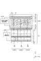
- FIG. 1 is a diagram showing a longitudinal sectional configuration of the semiconductor laser device according to the first embodiment.
- FIG. 2 is a diagram showing a vertical cross-sectional configuration of the semiconductor laser device according to the second embodiment.
- FIG. 3 is a diagram showing a vertical cross-sectional configuration of the semiconductor laser device according to the third embodiment.
- FIG. 4 is a perspective view of the semiconductor laser device (FIG. 4- (A)) and a plan view of the semiconductor laser unit as a unit element (FIG. 4- (B)).
- FIG. 5 is a plan view of the diffraction grating layer.
- FIG. 1 is a diagram showing a vertical cross-sectional configuration of the semiconductor laser device according to the first embodiment.
- the semiconductor laser chip LDC (N) is shown as a completely separated chip, but these may be formed on a common substrate and an isolation structure may be provided between the chips. In both the complete separation and the isolation separation, each semiconductor laser chip LDC (N) functions as a semiconductor laser unit.
- the semiconductor laser chip LDC includes a light emitting layer including the active layer 4, a pair of cladding layers 2 and 7 sandwiching the light emitting layer, and a diffraction grating layer 6 optically coupled to the light emitting layer.
- the light emitting layer includes an active layer 4 and light guide layers 3 and 5 sandwiching the active layer as necessary.
- Each semiconductor laser chip LDC includes a semiconductor substrate 1.
- the thickness direction of the semiconductor substrate 1 is taken as the Z axis, and the two directions perpendicular thereto are taken as the X axis and the Y axis.
- each semiconductor layer is epitaxially grown sequentially on the surface in the ⁇ Z-axis direction of the semiconductor substrate 1.
- the lower clad layer 2 the light emitting layer (light guide layer 3, active layer 4, light guide layer 5), diffraction grating layer 6, upper clad are formed on the semiconductor substrate 1.
- Layer 7 and contact layer 8 are sequentially formed.
- a drive electrode E3 is formed on the surface of the semiconductor substrate 1 on the + Z axis side
- an electrode E2 is formed on the surface of the contact layer 8 on the ⁇ Z axis side.
- These electrodes E3 and E2 are drive electrodes, and the drive electrodes have a plurality of openings such as stripes or meshes extending over the entire surface of the semiconductor substrate, or are made of transparent electrodes.
- each light emitting layer When a current is supplied from the laser drive circuit L-DR between the drive electrode E3 and the second electrode E2 of each semiconductor laser chip LDC, each light emitting layer emits light independently. That is, when a drive current is supplied between the drive electrode E3 and the second electrode E2, recombination of electrons and holes occurs in the active layer 4, and the active layer 4 emits light.
- the carriers contributing to the light emission and the generated light are efficiently confined between the upper and lower light guide layers 3 and 5 and the cladding layers 2 and 7.
- the laser beam LB generated in the light emitting layer propagates in the diffraction grating layer 6, and the diffraction grating layer 6 emits the laser beam in a direction perpendicular to the thickness direction, that is, in the Z-axis direction.
- the laser light emitted from the diffraction grating layer 6 travels in the + Z-axis direction and enters the spatial light modulator SLM via the cladding layer 2 and the semiconductor substrate 1.
- the spatial light modulator SLM is attached to a group of semiconductor laser chips LDC so that the laser light LB output along the thickness direction of the diffraction grating layer 6 is input.
- the laser light is incident on the liquid crystal layer LC via the transparent one of the common electrode 25 and the pixel electrode 21 of the spatial light modulator SLM. These electrode positions can be switched, and the pixel electrode 21 can also be made transparent.
- the spatial light modulator SLM modulates the phase of each minute region of the laser light LB with a drive voltage applied between the pixel electrode and the common electrode, reflects the phase-modulated laser light, and converts the semiconductor laser chip Output to the outside.
- the laser light LB output from the spatial light modulator SLM is superposed with the phase of each minute region adjusted to form various laser beam patterns.
- a far field image of the superimposed laser beam LB can constitute a specific character.
- the beam direction can be changed by the spatial light modulator SLM, and a plurality of deflected laser light beams enter the pupil of the eye.
- the width L (array period) in the X-axis direction of the semiconductor laser chip LDC is set to 2.5 mm or less.
- the width d (pitch) in the X-axis direction of the pixel electrode 21 of the spatial light modulator SLM is set to 60 ⁇ m or less.
- the semiconductor laser device is disposed on the semiconductor laser chip LDC and applies a spatial light modulator drive circuit S-DR (row selection circuit) that selectively applies a drive voltage between a pixel electrode and a common electrode located at a desired address. , Including a column selection circuit).
- S-DR row selection circuit
- the spatial light modulator can be controlled without installing a large-scale external wiring group.
- the spatial light modulator SLM includes a transparent common electrode 25, a plurality of transparent pixel electrodes 21, and a liquid crystal layer LC disposed between the common electrode 25 and the pixel electrode 21.
- the common electrode 25 is formed on the transparent substrate TS.
- the liquid crystal layer LC is made of nematic liquid crystal or ferroelectric liquid crystal.
- a drive current is supplied from the drive circuit to the semiconductor laser chip constituting the semiconductor laser element via the drive electrode.
- the laser beam LB is output from the light emitting layer, and the laser beam LB reaches the liquid crystal layer LC through the pixel electrode 21 of the spatial light modulator and is phase-modulated by the liquid crystal layer LC, and then is reflected by the reflecting mirror or the reflecting film.
- the common electrode 25 is connected to a fixed potential (ground), and the pixel electrode 21 is connected to a row selection circuit via a switch element and a row line.
- a column line extends from the column selection circuit and is connected to the control terminal of the switch element.
- This switch element is a field effect transistor. In this case, the control terminal is the gate of the transistor.
- the spatial light modulator when a specific address (x, y) is designated, an ON signal is output from the column selection circuit to the column line at the coordinate x, and a desired potential is applied from the row selection circuit to the row line at the coordinate y. It is done. In this case, a drive voltage is applied between the pixel electrode 21 at the address (x, y) and the common electrode 25, the refractive index of the liquid crystal layer changes, the optical path length changes, and the laser light The phase is adjusted.
- the row direction and the column direction are determined by the subjectivity, and are directions that can be replaced with each other.
- the magnitude of the drive voltage is determined by the output potential from the row selection circuit and the output potential of the column selection circuit, and can be constant. However, when performing more precise phase control, for example, A variable resistor may be connected to each switch element, and the value of the variable resistor may be controlled by a selection circuit having a similar configuration.
- phase distribution of the spatial light modulator is measured in advance so that the device outputs a desired pattern even when the phase of the spatial light modulator has variations in the plane during manufacturing.
- a drive circuit for a spatial light modulator that generates a drive voltage applied to each pixel electrode via a selection circuit based on data stored in the storage device. That is, this semiconductor laser device measures the phase distribution of the spatial light modulator in advance, stores the initial phase correction value for correcting the in-plane variation of the phase based on the measurement value, and stores the spatial light modulator. It is possible to provide a storage device for providing different initial phases for each pixel electrode. In other words, this device includes a storage device (not shown) that stores the initial correction value of the drive voltage for each pixel electrode.
- the drive voltage is applied from the control device (not shown) to the row selection circuit and the column selection circuit of the spatial light modulator drive circuit S-DR, and the drive voltage and the initial correction value are stored in the storage device. .
- the reference phase distribution and the measured phase distribution are compared, and the drive voltage value corresponding to the phase difference for each pixel can be used as the initial correction value.
- the drive voltage of the initial correction value is applied to the pixel electrode. If given, a reference phase distribution is realized. In order to obtain a desired phase distribution, the desired drive voltage can be superimposed on the drive voltage corresponding to the initial correction value.
- this semiconductor laser device preliminarily assumes each phase of the spatial light modulator, assuming that the polarization state is disturbed by transmitting the liquid crystal, and as a result, the intensity of the light output obtained by transmitting through the polarizing plate changes.
- a correction circuit for correcting the drive current applied to the semiconductor laser chip LDC for each phase pattern on the basis of the storage device for measuring the intensity of the output light and correcting the intensity. You may prepare.
- this apparatus includes a correction circuit (not shown) for correcting a drive current for each semiconductor laser chip, and a semiconductor laser chip for each phase pattern of all pixels included in a range corresponding to each semiconductor laser chip.
- a storage device (not shown) that stores a correction value of a current value for correcting a drive current applied to the LDC can be provided. According to this, at each moment (within each frame), for each semiconductor laser chip LDC, the drive current can be corrected according to the phase pattern of all the pixels corresponding to each semiconductor laser chip LDC, and the liquid crystal It is possible to realize a uniform light amount distribution that is not affected by the disturbance of the polarization state due to transmission.
- the laser light output from the diffraction grating layer 6 in the thickness direction reaches the liquid crystal layer LC via the common electrode 25 (or the pixel electrode 21 when the position is replaced with the pixel electrode).
- the dielectric constant (refractive index) of the liquid crystal layer LC changes depending on the voltage applied to the pixel electrode 21. Therefore, the optical path length of the liquid crystal layer LC with respect to the laser light changes, and the phase changes.
- the phase of the laser beam LB that has passed through the liquid crystal layer LC and reciprocated is modulated for each pixel electrode 21. Therefore, wavefront control can be performed for each minute region, and a desired laser beam pattern that can be changed can be formed by overlapping the wavefronts.
- a transparent insulating film (antireflection film) 9 made of SiO 2 or SiNx is formed on the drive electrode E3.
- the quarter wavelength plate 26, the transparent substrate TS, and the common electrode 25 of the spatial light modulator SLM are disposed.
- a frame-like spacer 24 for holding liquid crystal is provided on the common electrode 25, and a space inside the spacer 24 is filled with a liquid crystal layer LC.
- a reflective film 23 is formed on the spacer 24 and the liquid crystal layer LC, and a plurality of pixel electrodes 21 are disposed on the reflective film 23 with a protective film 22 interposed therebetween.
- the pixel electrode 21 is located between the substrate 20 and the protective film 22.
- the pixel electrode 21 is preferably formed on the substrate 20 made of a semiconductor, and then the protective film 22 is covered with the protective film 22 so that the surface thereof is planarized.
- a reflective film 23 is formed on the film 22, and the intermediate substrate is inverted and placed on the frame-like spacer 24.
- Appropriate alignment films are provided on the upper and lower surfaces of the liquid crystal layer LC.
- the laser beam LB reflected by the reflective film 23 on the liquid crystal layer LC is output to the outside through the common electrode 25 and the semiconductor laser chip LDC.
- the light emitting layer is composed of the active layer 4 and the light guide layers 3 and 5 sandwiching the active layer 4, and the contact layer 8 is provided as necessary.
- the semiconductor laser chip includes a laser light generation region LD in which an active layer 4 is formed, and the diffraction grating layer 6 is located in the laser light generation region LD, and laser is directed toward the thickness direction of the diffraction grating layer 6.
- Light LB is emitted.
- the spatial light modulator SLM is mounted on the laser light generation region LD. In the case of this structure, the apparatus can be reduced in size by arranging the spatial light modulator SLM on the laser light generation region LD.
- a drive electrode E3 is disposed on the + Z side surface of the semiconductor substrate 1.
- This semiconductor laser device includes a semiconductor laser chip LDC and a spatial light modulator SLM optically coupled to the semiconductor laser chip LDC, and converts the laser light LB output along the thickness direction of the semiconductor laser chip LDC into spatial light.
- a semiconductor laser device that modulates with a modulator SLM and outputs to the outside, the semiconductor laser chip LDC is optically connected to the active layer 4, a pair of clad layers 2 and 7 sandwiching the active layer 4, and the active layer 4.
- a driving electrode E3 disposed between the cladding layer 2 on the spatial light modulator SLM side and the spatial light modulator SLM and for supplying a current to the active layer 4. Yes.
- the thickness direction of the semiconductor laser chip LDC is the Z-axis direction
- the plane parallel to the interface between the semiconductor laser chip LDC and the spatial light modulator SLM is the XY plane.
- the drive electrode E3 is located in the XY plane.
- the drive electrode E3 has a plurality of openings as viewed from the Z-axis direction, and the drive electrode E3 has a non-periodic structure, but is composed of a transparent electrode made of ITO or the like (indium tin oxide). You can also
- a metal such as Ag or Au can be used as the material of the conductive region constituting the drive electrode.
- a transparent electrode such as ITO, ZnO, graphene, or Ag nanowire
- a low-resistance material is preferable, so a stripe or mesh-shaped opening is preferable to the transparent electrode.
- an opaque metal material having
- a transparent insulating film 9 is formed on the drive electrode.
- the spatial light modulator SLM is provided on the drive electrode E3.
- the row selection circuit and the column selection circuit (not shown) are located outside the drive electrode E3, appropriate connection wirings are provided from these to the pixel electrode and the common electrode.
- the electrode E2 is configured to transmit part or all of the laser beam LB.
- the electrode E2 can adopt the same structure as that of the drive electrode E3.
- the diffraction grating layer 6 has a structure in which, for example, triangular shapes are arranged in a square lattice pattern, and diffracts linearly polarized light in the vertical direction. If the polarization transmission axis of linearly polarized light output from the diffraction grating layer 6 at this time is the axis A, the polarization transmission axis of the polarizing plate 27 is set in a direction orthogonal to the axis A (referred to as axis B). Further, the fast axis of the quarter wave plate is set in a direction rotated by 45 ° from the axis A.
- the laser beam that has entered the spatial light modulator SLM via the quarter-wave plate 26, reciprocated through the spatial light modulator SLM, and again passed through the quarter-wave plate 26 in the opposite direction has a polarization orientation of 90. Rotate degrees. That is, when the laser beam LB is incident on the quarter-wave plate 26 as linearly polarized light having the first polarization direction (axis A), after passing through the quarter wavelength plate 26, the laser light LB changes in the first polarization direction. On the other hand, it becomes linearly polarized light having the second polarization direction (axis B) rotated by 90 degrees.
- the polarization direction in the polarizing plate 27 is matched with the second polarization direction (axis B)
- only the laser light reciprocating through the spatial light modulator SLM is transmitted through the polarizing plate 27, and components in other polarization directions. Is blocked by the polarizing plate 27. Therefore, noise components that are not modulated by the liquid crystal layer LC are removed from the output image, and the contrast is improved.
- the positions of the common electrode 25 and the quarter-wave plate 26 can be interchanged.
- FIG. 5 is a plan view of the diffraction grating layer.
- the above-described diffraction grating layer 6 includes, for example, a basic layer 6A and a different refractive index region 6B.
- the different refractive index region 6B is embedded in the basic layer 6A at a predetermined depth, and the refractive index is different from this.
- the planar shape of the different refractive index region 6B is circular, but other shapes such as a triangle and an ellipse may be used. For example, in order to increase the intensity in a specific polarization direction, the shape may not have 90 degree rotational symmetry. In order to obtain linearly polarized light, this shape can be, for example, an isosceles triangle, a right triangle, or a right isosceles triangle.
- the different refractive index region 6B is arranged at the lattice point position of the square lattice, but it may be arranged at the lattice point position of the triangular lattice.
- the diffraction grating layer 6 has a periodic structure in which the refractive index changes two-dimensionally by embedding the different refractive index region, it functions as a diffraction grating and also as a photonic crystal layer.
- a periodic structure in which perfect circular holes are arranged in a square lattice is used, but a periodic structure in which triangular holes are arranged in a square lattice may be used, and the semiconductor laser element is a surface emitting laser. Function.
- the semiconductor substrate 1 is made of GaAs
- the lower cladding layer 2 is made of AlGaAs
- the lower light guide layer 3 is made of AlGaAs
- the active layer 4 is a multiquantum.
- the well structure MQW carrier layer: AlGaAs / well layer: InGaAs
- the upper light guide layer 5 is made of lower layer AlGaAs / upper layer GaAs
- the upper cladding layer 7 is made of AlGaAs
- the contact layer 8 is made of GaAs.
- the basic layer 6A is made of GaAs, and the different refractive index region (buried layer) 6B embedded in the basic layer 6A is made of AlGaAs.
- the first conductivity type (N-type) impurity or the second conductivity type (P-type) impurity is added to each layer (impurity concentration is 1 ⁇ 10 17 to 1 ⁇ 10 21 / cm 3 ).
- the semiconductor substrate 1 is N type
- the lower cladding layer 2 is N type
- the lower light guide layer 3 is I type
- the active layer 4 is I type
- the lower layer of the upper light guide layer 5 is P or I type
- the upper layer is I type
- the diffraction grating layer 6 can be I-type
- the upper cladding layer 7 can be P-type
- the contact layer 8 can be P-type.
- a region to which no impurity is intentionally added is intrinsic (I type).
- the I-type impurity concentration is 1 ⁇ 10 16 / cm 3 or less.
- the thickness of the semiconductor substrate 1 is 150 ⁇ m (80 ⁇ m to 350 ⁇ m)
- the thickness of the lower cladding layer 2 is 2 ⁇ 10 3 nm (1 ⁇ 10 3 nm to 3 ⁇ 10 3 nm)
- the thickness of the active layer 4 is 30 nm (10 nm to 100 nm)
- the thickness of the lower layer of the upper light guide layer 5 is 50 nm (10 nm to 100 nm)
- the thickness of the upper layer is 50 nm (10 nm to 200 nm)
- the thickness of the lattice layer 6 is 100 nm (50 nm to 200 nm)
- the thickness of the upper cladding layer 7 is 2 ⁇ 10 3 nm (1 ⁇ 10 3 nm to 3 ⁇ 10 3 nm)
- the thickness of the contact layer 8 is 200 nm (50 nm to 500 nm).
- the energy band gap of the cladding layer is larger than the energy band gap of the light guide layer, and the energy band gap of the light guide layer is set larger than the energy band gap of the well layer of the active layer 4.
- the energy band gap and the refractive index can be easily changed by changing the Al composition ratio.
- Al X Ga 1-X As when the composition ratio X of Al having a relatively small atomic radius is decreased (increased), the energy band gap that is positively correlated with this decreases (increases), and GaAs has an atomic radius. When large In is mixed to make InGaAs, the energy band gap becomes small.
- the Al composition ratio of the cladding layer is larger than the Al composition ratio of the light guide layer, and the Al composition ratio of the light guide layer is equal to or larger than the barrier layer (AlGaAs) of the active layer.
- the Al composition ratio of the cladding layer is set to 0.2 to 0.4, and is 0.3 in this example.
- the Al composition ratio of the barrier layer in the light guide layer and the active layer is set to 0.1 to 0.15, and is 0.1 in this example.
- a layer of about 10 to 100 nm with an Al composition equivalent to that of the cladding layer is inserted between the second conductivity type (p-type) cladding layer. May be.
- a columnar different refractive index region in the diffraction grating layer 6 may be a gap and a gas such as air, nitrogen, or argon may be enclosed.
- a different refractive index region 6 ⁇ / b> B is disposed at a lattice point position of a square lattice or a triangular lattice in the XY plane.
- the interval between the vertical and horizontal lattice lines in this square lattice is about the wavelength of the laser beam divided by the equivalent refractive index, and is specifically set to about 300 nm.
- the different refractive index regions can be arranged not at the lattice point positions of the square lattice but at the lattice point positions of the triangular lattice.
- the interval between the horizontal and oblique lattice lines is a value obtained by dividing the wavelength by the equivalent refractive index and further dividing by Sin 60 °, and is preferably set to about 350 nm.
- the common electrode and the pixel electrode described above are made of ITO or ZnO when they are transparent. Such a material is transparent to the laser beam and can transmit the laser beam.
- the material of the high refractive index material layer (nH) is at least one material (for example, Ta 2 ) selected from an oxide group (insulator group) made of Ta 2 O 5 , TiO 2 , Nb 2 O 5, HfO 2, and the like. O 5 ).
- the material of the low refractive index material layer (nL) includes at least one material (for example, SiO 2 ) selected from an insulator group made of SiO 2, MgF 2, and the like.
- the optical film thicknesses of the high refractive material layer (nH) and the low refractive index material layer (nL) are set to 1 ⁇ 4 of the wavelength ⁇ of the laser light.
- the laminated structure of these dielectric layers the following types can be considered.
- the total number of layers is 2 ⁇ A ⁇ m.
- m is a natural number.
- the lowermost layer is a low refractive index material layer (nL).
- the low refractive index material layer (nL) is further formed on the high refractive material layer (nH) located on the outermost surface.
- the total number of layers is 2 ⁇ A ⁇ m + 1.
- each compound semiconductor layer uses a metal organic chemical vapor deposition (MOCVD) method. Although crystal growth is performed on the (001) plane of the semiconductor substrate 1, it is not limited to this.
- MOCVD metal organic chemical vapor deposition
- the growth temperature of AlGaAs is 500 ° C. to 850 ° C., and 550 to 700 ° C. is used in the experiment, and TMA (trimethylaluminum), gallium raw material is used as the Al raw material during growth.
- TMG trimethyl gallium
- TEG triethyl gallium
- As raw material AsH 3 arsine
- N-type impurity raw material Si 2 H 6 dilane
- P-type impurity raw material DEZn diethyl zinc Is used.
- TMA trimethyl gallium
- TMG triethyl gallium
- AsH 3 arsine
- Si 2 H 6 dilane
- P-type impurity raw material DEZn diethyl zinc
- InGaAs is manufactured using TMG, TMI (trimethylindium), and arsine.
- the insulating film may be formed by sputtering a target using the constituent material as a raw material.
- an N-type cladding layer (AlGaAs) 2 is first formed on an N-type semiconductor substrate (GaAs) 1, and then an optical guide layer (AlGaAs) 3 and a multiple quantum well structure (InGaAs / AlGaAs) 4 and light guide layer (GaAs / AaGaAs) 5 are formed, and then a basic layer (GaAs) 6A to be a photonic crystal layer is epitaxially grown sequentially using MOCVD (metal organic chemical vapor deposition). .
- MOCVD metal organic chemical vapor deposition
- a SiN layer is formed on the basic layer 6A by PCVD (plasma CVD), and then a resist is formed on the SiN layer. Further, the resist is exposed and developed, the SiN layer is etched using the resist as a mask, and a part of the SiN layer is left to form an alignment mark. The remaining resist is removed.
- PCVD plasma CVD
- a two-dimensional fine pattern is formed on the resist by drawing and developing a two-dimensional fine pattern on the resist using an electron beam drawing apparatus with reference to the alignment mark.
- a two-dimensional fine pattern having a depth of about 100 nm is transferred onto the basic layer 6A by dry etching to form a hole (hole), and the resist is removed.
- the depth of the hole is 100 nm.
- the compound semiconductor that becomes the different refractive index region 6B AlGaAs
- an upper cladding layer (AlGaAs) 7 and a contact layer (GaAs) 8 are sequentially formed by MOCVD, and an appropriate electrode material is formed on the upper and lower surfaces of the substrate by vapor deposition or sputtering to form first and second electrodes. Form. Further, if necessary, insulating films can be formed on the upper and lower surfaces of the substrate by sputtering or the like.
- the diffraction grating layer 6 When the diffraction grating layer 6 is provided below the active layer, the diffraction grating layer may be formed on the lower cladding layer before the formation of the active layer and the lower light guide layer.
- a quarter-wave plate 26 is disposed on the semiconductor substrate 1 with an insulating film 9 interposed therebetween, and a polarizing plate 27 is disposed on the surface of the contact layer 8.
- the drive electrode E3 is formed on the semiconductor substrate 1, patterning is performed on the semiconductor substrate 1 using a photolithography method.
- the light generated in the active layer is modulated by the diffraction grating layer and oscillated in a two-dimensional single mode, and a part of the oscillated light is generated by the diffraction grating layer. It receives second-order diffraction and is incident on the liquid crystal layer as a plane wave. Since the liquid crystal has refractive index anisotropy, the equivalent refractive index in the direction parallel to the light output changes according to the rotation angle. At this time, since the physical length of the liquid crystal layer is constant, the optical path length changes as the refractive index changes. Accordingly, when a plane wave is incident on the liquid crystal layer from below, the optical path length can be changed for each pixel.
- FIG. 4 is a perspective view of the semiconductor laser device (FIG. 4- (A)) and a plan view of the semiconductor laser unit as a unit element (FIG. 4- (B)).
- the first laser light LB output from one semiconductor laser chip LDC is incident on the right eye R-Eye of the observer, and the second laser light LB output from another semiconductor laser chip LDC is the observer. Enters the left eye L-Eye. Since the laser beam LB incident on the right eye and the laser beam LB incident on the left eye can be controlled independently, a three-dimensional image can be formed.
- FIG. 2 is a view showing a vertical cross-sectional configuration of the semiconductor laser device according to the second embodiment.
- a plurality of semiconductor laser chips (semiconductor laser units) LDC include a first semiconductor laser unit LDC (1) that outputs laser light LB having a first wavelength (Red), and a second wavelength (Green).
- These first, second, and third wavelengths are different from each other, and three or more types of wavelengths can be used.
- this semiconductor laser device by using laser beams having three or more types of wavelengths, stereoscopic images of various colors can be formed by superimposing the laser beams.
- FIG. 3 is a view showing a vertical cross-sectional configuration of the semiconductor laser device according to the third embodiment.
- the plurality of semiconductor laser chips (semiconductor laser units) LDC are, in addition to those of the second embodiment, a fourth semiconductor laser unit that outputs a laser beam LB having a fourth wavelength (Cyan).
- These first, second, third, fourth, fifth and sixth wavelengths are different from each other, and six or more wavelengths can be used.
- this semiconductor laser device it is possible to form stereoscopic images of various colors by using laser beams having six or more wavelengths.
- the semiconductor laser device described above includes a semiconductor including a plurality of semiconductor laser units LDC that can be independently driven and a spatial light modulator SLM optically coupled to a group of the plurality of semiconductor laser units LDC.
- the laser device includes the following elements.
- Each semiconductor laser unit LDC includes an active layer 4, a pair of cladding layers 2 and 7 sandwiching the active layer 4, and a diffraction grating layer 6 optically coupled to the active layer 4.
- the semiconductor laser unit LDC outputs laser light along each thickness direction.
- the spatial light modulator SLM includes a liquid crystal layer LC, a reflective film 23 provided on the opposite side of the liquid crystal layer LC from the semiconductor laser portion LDC, a plurality of pixel electrodes 21 arranged in a two-dimensional manner, The pixel electrode 21 and a common electrode sandwiching the liquid crystal layer LC are provided, and the width d of each pixel electrode 21 is 1 ⁇ 2 or less of the width L of each semiconductor laser portion LDC.
- each semiconductor laser unit LDC enters the spatial light modulator SLM, and is modulated according to the state of the liquid crystal layer LC by each pixel electrode 21, and the spatial light modulator SLM
- the laser light reflected and modulated by the reflective film 23 passes through each semiconductor laser unit LDC again from the light emitting surface (surface on the ⁇ Z axis side of the polarizing plate 27) of each semiconductor laser unit LEC to the outside. Is output.
- the semiconductor laser device includes a quarter wavelength plate (phase difference plate) 26 disposed between the group of active layers 4 of the plurality of semiconductor laser units LDC and the reflective film 23, and a plurality of semiconductor laser units LDC. And a polarizing plate 27 disposed between the group of active layers 4 and the light exit surface.
- the polarizing plate 27 is a single sheet and covers all the semiconductor laser portions LDC, but this may be separated for each semiconductor laser portion.
- the laser beam output from the semiconductor laser unit LDC which is a surface emitting laser element is emitted along the thickness direction, reflected by the reflection film 23 of the spatial light modulator SLM, and the liquid crystal layer LC. And the phase is modulated and output to the outside via the polarizing plate 27. Therefore, the direction of the output laser light that is phase-modulated from the polarizing plate for each pixel differs depending on the intensity of modulation by the liquid crystal layer LC.
- Laser light that is about to be emitted from the semiconductor laser unit LDC without passing through the spatial light modulator SLM can be suppressed by the polarizing plate 27. In other words, the laser light that has entered the spatial light modulator SLM and reflected to pass through the quarter-wave plate 26 twice has the phase reversed and the polarization orientation rotated by 90 degrees. The light passes through the polarizing plate 27.
- the polarization direction of the laser light in the active layer 4 is the first direction (A)
- the polarization direction (B) transmitted by the polarizing plate 27 is orthogonal to the first direction (A)
- the laser light is directly Cannot pass through the waveplate.
- the laser beam that has passed through the quarter-wave plate twice has a polarization direction (B) orthogonal to the first direction (A) and passes through the polarizing plate 27 in the absence of the liquid crystal layer LC. Can do. Only a polarization component whose phase is adjusted by the liquid crystal layer LC by applying a bias voltage between the pixel electrode 21 and the common electrode 25 is transmitted through the polarizing plate 27.
- the width of the pixel electrode is smaller than each semiconductor laser portion, and two or more pixel electrodes are arranged corresponding to a single semiconductor laser portion.
- the light generated in each semiconductor laser unit LDC undergoes two-dimensional phase modulation for each pixel of the spatial light modulator SLM after reciprocating the spatial light modulator SLM.
- a beam is generated for each semiconductor laser unit LDC.
- the pattern can be controlled. Therefore, it is possible to output a unimodal beam in any direction for each semiconductor laser unit LDC by giving a signal to the spatial light modulator drive circuit S-DR so as to give a unidirectional beam whose direction is controlled as an output beam pattern.
- the arrangement period L of the semiconductor laser portion LDC at this time to half or less of the pupil diameter of the eye, a natural stereoscopic image by the integral method can be formed.
- the maximum diffraction angle ⁇ of the unidirectional beam in any direction from each semiconductor laser unit LDC can be expressed as ⁇ / d. In order to obtain it, it is necessary to set an appropriately small d.
- a single peak beam in an arbitrary direction is output for each semiconductor laser unit LDC.
- the pixel pitch d is an appropriate number
- an arbitrary beam pattern can be obtained for each LDC.
- a plurality of arbitrary direction beams can be obtained for each semiconductor laser unit LDC.
- the number of viewpoints when a natural stereoscopic image display is formed can be increased.
- the frame rate can be increased with the same number of viewpoints.
- the liquid crystal layer LC may be rotated by 90 degrees with no bias or may be rotated by 0 degrees. In either case, it can be adjusted to a desired polarization orientation by applying a bias voltage to the pixel electrode.
- SLM Spatial light modulator
- LDC Semiconductor laser chip (semiconductor laser part)
- 4 Active layer
- 2, 7 Cladding layer
- 6 Diffraction grating layer.
Landscapes
- Physics & Mathematics (AREA)
- General Physics & Mathematics (AREA)
- Optics & Photonics (AREA)
- Condensed Matter Physics & Semiconductors (AREA)
- Electromagnetism (AREA)
- Nonlinear Science (AREA)
- Mathematical Physics (AREA)
- Chemical & Material Sciences (AREA)
- Crystallography & Structural Chemistry (AREA)
- Liquid Crystal (AREA)
- Optical Modulation, Optical Deflection, Nonlinear Optics, Optical Demodulation, Optical Logic Elements (AREA)
- Semiconductor Lasers (AREA)
Abstract
Description
Claims (4)
- 独立駆動可能な複数の半導体レーザ部と、
複数の前記半導体レーザ部のグループに光学的に結合した空間光変調器と、を備えた半導体レーザ装置であって、
個々の前記半導体レーザ部は、
活性層と、
前記活性層を挟む一対のクラッド層と、
前記活性層に光学的に結合した回折格子層と、
を備え、
複数の前記半導体レーザ部は、それぞれの厚み方向に沿ってレーザ光を出力し、
前記空間光変調器は、
液晶層と、
前記液晶層の前記半導体レーザ部とは反対側に設けられた反射膜と、
二次元状に配置された複数の画素電極と、
前記画素電極と共に前記液晶層を挟む共通電極と、
を備え、
それぞれの前記半導体レーザ部から出射されたレーザ光は、前記空間光変調器内に入射し、それぞれの前記画素電極による前記液晶層の状態に応じて変調され、
前記空間光変調器の前記反射膜で反射され、変調されたレーザ光は、それぞれの前記半導体レーザ部を再度介して、それぞれの前記半導体レーザ部の光出射面から外部に出力され、
前記半導体レーザ装置は、
複数の前記半導体レーザ部の前記活性層のグループと前記反射膜との間に配置された1/4波長板と、
複数の前記半導体レーザ部の前記活性層のグループと前記光出射面との間に配置された偏光板と、を備えることを特徴とする半導体レーザ装置。 - 個々の前記画素電極の幅は、個々の半導体レーザ部の幅の1/2以下である、ことを特徴とする請求項1に記載の半導体レーザ装置。
- 複数の前記半導体レーザ部は、
第1波長のレーザ光を出力する第1半導体レーザ部と、
第2波長のレーザ光を出力する第2半導体レーザ部と、
第3波長のレーザ光を出力する第3半導体レーザ部と、
を備え、
前記第1、第2、及び第3波長は、互いに異なっていることを特徴とする請求項1又は2に記載の半導体レーザ装置。 - 複数の前記半導体レーザ部は、
第4波長のレーザ光を出力する第4半導体レーザ部と、
第5波長のレーザ光を出力する第5半導体レーザ部と、
第6波長のレーザ光を出力する第6半導体レーザ部と、
を備え、
前記第1、第2、第3、第4、第5及び第6波長は、互いに異なっていることを特徴とする請求項3に記載の半導体レーザ装置。
Priority Applications (2)
| Application Number | Priority Date | Filing Date | Title |
|---|---|---|---|
| DE112016000302.1T DE112016000302B4 (de) | 2015-01-09 | 2016-01-07 | Halbleiterlaservorrichtung |
| US15/541,515 US10090636B2 (en) | 2015-01-09 | 2016-01-07 | Semiconductor laser device |
Applications Claiming Priority (2)
| Application Number | Priority Date | Filing Date | Title |
|---|---|---|---|
| JP2015-003557 | 2015-01-09 | ||
| JP2015003557A JP6489836B2 (ja) | 2015-01-09 | 2015-01-09 | 半導体レーザ装置 |
Publications (1)
| Publication Number | Publication Date |
|---|---|
| WO2016111332A1 true WO2016111332A1 (ja) | 2016-07-14 |
Family
ID=56356017
Family Applications (1)
| Application Number | Title | Priority Date | Filing Date |
|---|---|---|---|
| PCT/JP2016/050370 Ceased WO2016111332A1 (ja) | 2015-01-09 | 2016-01-07 | 半導体レーザ装置 |
Country Status (4)
| Country | Link |
|---|---|
| US (1) | US10090636B2 (ja) |
| JP (1) | JP6489836B2 (ja) |
| DE (1) | DE112016000302B4 (ja) |
| WO (1) | WO2016111332A1 (ja) |
Cited By (16)
| Publication number | Priority date | Publication date | Assignee | Title |
|---|---|---|---|---|
| WO2018181202A1 (ja) * | 2017-03-27 | 2018-10-04 | 浜松ホトニクス株式会社 | 半導体発光素子およびその製造方法 |
| JP2019106397A (ja) * | 2017-12-08 | 2019-06-27 | 浜松ホトニクス株式会社 | 発光装置 |
| US20190312410A1 (en) * | 2017-03-27 | 2019-10-10 | Hamamatsu Photonics K.K. | Semiconductor light-emitting module and control method therefor |
| CN110383609A (zh) * | 2017-03-27 | 2019-10-25 | 浜松光子学株式会社 | 半导体发光模块及其控制方法 |
| JP2019201065A (ja) * | 2018-05-15 | 2019-11-21 | 浜松ホトニクス株式会社 | 発光デバイス |
| JP2020507202A (ja) * | 2016-12-29 | 2020-03-05 | エックス デベロップメント エルエルシー | 集積デジタルレーザ |
| US10734786B2 (en) | 2016-09-07 | 2020-08-04 | Hamamatsu Photonics K.K. | Semiconductor light emitting element and light emitting device including same |
| US11031747B2 (en) | 2016-08-10 | 2021-06-08 | Hamamatsu Photonics K.K. | Light-emitting device |
| US11031751B2 (en) | 2016-08-10 | 2021-06-08 | Hamamatsu Photonics K.K. | Light-emitting device |
| WO2021149389A1 (ja) * | 2020-01-20 | 2021-07-29 | ソニーセミコンダクタソリューションズ株式会社 | 発光装置 |
| US11626709B2 (en) | 2017-12-08 | 2023-04-11 | Hamamatsu Photonics K.K. | Light-emitting device and production method for same |
| US11646546B2 (en) | 2017-03-27 | 2023-05-09 | Hamamatsu Photonics K.K. | Semiconductor light emitting array with phase modulation regions for generating beam projection patterns |
| US11686956B2 (en) | 2017-06-15 | 2023-06-27 | Hamamatsu Photonics K.K. | Light-emitting device |
| WO2023171629A1 (ja) * | 2022-03-09 | 2023-09-14 | 浜松ホトニクス株式会社 | 半導体発光素子 |
| JP7482202B1 (ja) | 2022-12-22 | 2024-05-13 | エルジー ディスプレイ カンパニー リミテッド | 空間光変調器及び立体映像装置 |
| US12126140B2 (en) | 2018-06-08 | 2024-10-22 | Hamamatsu Photonics K.K. | Light-emitting element |
Families Citing this family (7)
| Publication number | Priority date | Publication date | Assignee | Title |
|---|---|---|---|---|
| JP6747922B2 (ja) * | 2016-09-07 | 2020-08-26 | 浜松ホトニクス株式会社 | 半導体発光素子及び発光装置 |
| US10270221B1 (en) * | 2018-04-27 | 2019-04-23 | Avago Technologies International Sales Pte. Limited | Optical device and system having an array of addressable apertures |
| JP6891870B2 (ja) * | 2018-12-28 | 2021-06-18 | セイコーエプソン株式会社 | プロジェクター |
| US12181273B2 (en) * | 2020-02-21 | 2024-12-31 | Hamamatsu Photonics K.K. | Three-dimensional measurement device |
| US20220344905A1 (en) * | 2021-04-21 | 2022-10-27 | Osram Opto Semiconductors Gmbh | Semiconductor laser device and projection device |
| JP7828198B2 (ja) * | 2022-03-09 | 2026-03-11 | 浜松ホトニクス株式会社 | 位相分布設計方法、位相分布設計装置、位相分布設計プログラム及び記録媒体 |
| US20240396301A1 (en) * | 2023-05-22 | 2024-11-28 | Apple Inc. | Dynamic control of laser transverse mode |
Citations (12)
| Publication number | Priority date | Publication date | Assignee | Title |
|---|---|---|---|---|
| JP2002049002A (ja) * | 2000-08-03 | 2002-02-15 | Hamamatsu Photonics Kk | レーザ加工装置 |
| JP2002055322A (ja) * | 2000-08-09 | 2002-02-20 | Canon Inc | 液晶表示装置 |
| JP2002072206A (ja) * | 2000-09-04 | 2002-03-12 | Seiko Epson Corp | 液晶表示装置 |
| JP2002328630A (ja) * | 2001-02-20 | 2002-11-15 | Sharp Corp | 表示装置 |
| JP2005521197A (ja) * | 2002-03-18 | 2005-07-14 | コーニンクレッカ フィリップス エレクトロニクス エヌ ヴィ | 偏光光放出導波器、照明装置及び斯様な照明装置を有する表示装置 |
| JP2005277080A (ja) * | 2004-03-24 | 2005-10-06 | Toyota Central Res & Dev Lab Inc | 面発光半導体レーザ装置 |
| JP2007052160A (ja) * | 2005-08-17 | 2007-03-01 | Sanyo Epson Imaging Devices Corp | 表示装置 |
| JP2007328336A (ja) * | 2006-05-09 | 2007-12-20 | Victor Co Of Japan Ltd | 照明装置及び表示装置 |
| JP2008502925A (ja) * | 2004-05-28 | 2008-01-31 | イーストマン コダック カンパニー | 垂直キャビティ・レーザー・アレイを使用したディスプレイ・デバイス |
| JP2013522666A (ja) * | 2010-03-11 | 2013-06-13 | ピクストロニクス,インコーポレイテッド | ディスプレイ装置のための反射および半透過動作モード |
| WO2014175447A1 (ja) * | 2013-04-26 | 2014-10-30 | 浜松ホトニクス株式会社 | 半導体レーザ装置 |
| WO2015008627A1 (ja) * | 2013-07-16 | 2015-01-22 | 浜松ホトニクス株式会社 | 半導体レーザ装置 |
Family Cites Families (3)
| Publication number | Priority date | Publication date | Assignee | Title |
|---|---|---|---|---|
| US5301201A (en) * | 1993-03-01 | 1994-04-05 | At&T Bell Laboratories | Article comprising a tunable semiconductor laser |
| US7203210B2 (en) * | 2003-12-29 | 2007-04-10 | The Boeing Company | Methods and devices for forming a high-power coherent light beam |
| TW200641465A (en) * | 2005-05-20 | 2006-12-01 | Sanyo Epson Imaging Devices Co | Display device |
-
2015
- 2015-01-09 JP JP2015003557A patent/JP6489836B2/ja not_active Expired - Fee Related
-
2016
- 2016-01-07 WO PCT/JP2016/050370 patent/WO2016111332A1/ja not_active Ceased
- 2016-01-07 DE DE112016000302.1T patent/DE112016000302B4/de active Active
- 2016-01-07 US US15/541,515 patent/US10090636B2/en active Active
Patent Citations (12)
| Publication number | Priority date | Publication date | Assignee | Title |
|---|---|---|---|---|
| JP2002049002A (ja) * | 2000-08-03 | 2002-02-15 | Hamamatsu Photonics Kk | レーザ加工装置 |
| JP2002055322A (ja) * | 2000-08-09 | 2002-02-20 | Canon Inc | 液晶表示装置 |
| JP2002072206A (ja) * | 2000-09-04 | 2002-03-12 | Seiko Epson Corp | 液晶表示装置 |
| JP2002328630A (ja) * | 2001-02-20 | 2002-11-15 | Sharp Corp | 表示装置 |
| JP2005521197A (ja) * | 2002-03-18 | 2005-07-14 | コーニンクレッカ フィリップス エレクトロニクス エヌ ヴィ | 偏光光放出導波器、照明装置及び斯様な照明装置を有する表示装置 |
| JP2005277080A (ja) * | 2004-03-24 | 2005-10-06 | Toyota Central Res & Dev Lab Inc | 面発光半導体レーザ装置 |
| JP2008502925A (ja) * | 2004-05-28 | 2008-01-31 | イーストマン コダック カンパニー | 垂直キャビティ・レーザー・アレイを使用したディスプレイ・デバイス |
| JP2007052160A (ja) * | 2005-08-17 | 2007-03-01 | Sanyo Epson Imaging Devices Corp | 表示装置 |
| JP2007328336A (ja) * | 2006-05-09 | 2007-12-20 | Victor Co Of Japan Ltd | 照明装置及び表示装置 |
| JP2013522666A (ja) * | 2010-03-11 | 2013-06-13 | ピクストロニクス,インコーポレイテッド | ディスプレイ装置のための反射および半透過動作モード |
| WO2014175447A1 (ja) * | 2013-04-26 | 2014-10-30 | 浜松ホトニクス株式会社 | 半導体レーザ装置 |
| WO2015008627A1 (ja) * | 2013-07-16 | 2015-01-22 | 浜松ホトニクス株式会社 | 半導体レーザ装置 |
Cited By (25)
| Publication number | Priority date | Publication date | Assignee | Title |
|---|---|---|---|---|
| US11031751B2 (en) | 2016-08-10 | 2021-06-08 | Hamamatsu Photonics K.K. | Light-emitting device |
| US11031747B2 (en) | 2016-08-10 | 2021-06-08 | Hamamatsu Photonics K.K. | Light-emitting device |
| US10734786B2 (en) | 2016-09-07 | 2020-08-04 | Hamamatsu Photonics K.K. | Semiconductor light emitting element and light emitting device including same |
| JP2020507202A (ja) * | 2016-12-29 | 2020-03-05 | エックス デベロップメント エルエルシー | 集積デジタルレーザ |
| EP3563455A4 (en) * | 2016-12-29 | 2020-08-26 | X Development LLC | INTEGRATED DIGITAL LASER |
| CN110383610A (zh) * | 2017-03-27 | 2019-10-25 | 浜松光子学株式会社 | 半导体发光元件及其制造方法 |
| JPWO2018181202A1 (ja) * | 2017-03-27 | 2020-02-06 | 浜松ホトニクス株式会社 | 半導体発光素子およびその製造方法 |
| WO2018181202A1 (ja) * | 2017-03-27 | 2018-10-04 | 浜松ホトニクス株式会社 | 半導体発光素子およびその製造方法 |
| CN110383609A (zh) * | 2017-03-27 | 2019-10-25 | 浜松光子学株式会社 | 半导体发光模块及其控制方法 |
| US11637409B2 (en) | 2017-03-27 | 2023-04-25 | Hamamatsu Photonics K.K. | Semiconductor light-emitting module and control method therefor |
| US20190312410A1 (en) * | 2017-03-27 | 2019-10-10 | Hamamatsu Photonics K.K. | Semiconductor light-emitting module and control method therefor |
| US11777276B2 (en) | 2017-03-27 | 2023-10-03 | Hamamatsu Photonics K.K. | Semiconductor light emitting array with phase modulation regions for generating beam projection patterns |
| US11646546B2 (en) | 2017-03-27 | 2023-05-09 | Hamamatsu Photonics K.K. | Semiconductor light emitting array with phase modulation regions for generating beam projection patterns |
| JP7089504B2 (ja) | 2017-03-27 | 2022-06-22 | 浜松ホトニクス株式会社 | 半導体発光素子およびその製造方法 |
| US11686956B2 (en) | 2017-06-15 | 2023-06-27 | Hamamatsu Photonics K.K. | Light-emitting device |
| US11626709B2 (en) | 2017-12-08 | 2023-04-11 | Hamamatsu Photonics K.K. | Light-emitting device and production method for same |
| JP2019106397A (ja) * | 2017-12-08 | 2019-06-27 | 浜松ホトニクス株式会社 | 発光装置 |
| JP7219552B2 (ja) | 2018-05-15 | 2023-02-08 | 浜松ホトニクス株式会社 | 発光デバイス |
| JP2019201065A (ja) * | 2018-05-15 | 2019-11-21 | 浜松ホトニクス株式会社 | 発光デバイス |
| US12046874B2 (en) | 2018-05-15 | 2024-07-23 | Hamamatsu Photonics K.K. | Light-emitting device |
| US12126140B2 (en) | 2018-06-08 | 2024-10-22 | Hamamatsu Photonics K.K. | Light-emitting element |
| WO2021149389A1 (ja) * | 2020-01-20 | 2021-07-29 | ソニーセミコンダクタソリューションズ株式会社 | 発光装置 |
| WO2023171629A1 (ja) * | 2022-03-09 | 2023-09-14 | 浜松ホトニクス株式会社 | 半導体発光素子 |
| JP7482202B1 (ja) | 2022-12-22 | 2024-05-13 | エルジー ディスプレイ カンパニー リミテッド | 空間光変調器及び立体映像装置 |
| JP2024090285A (ja) * | 2022-12-22 | 2024-07-04 | エルジー ディスプレイ カンパニー リミテッド | 空間光変調器及び立体映像装置 |
Also Published As
| Publication number | Publication date |
|---|---|
| JP6489836B2 (ja) | 2019-03-27 |
| US20180006426A1 (en) | 2018-01-04 |
| DE112016000302T5 (de) | 2017-10-05 |
| JP2016129208A (ja) | 2016-07-14 |
| US10090636B2 (en) | 2018-10-02 |
| DE112016000302B4 (de) | 2025-05-28 |
Similar Documents
| Publication | Publication Date | Title |
|---|---|---|
| JP6489836B2 (ja) | 半導体レーザ装置 | |
| JP6401701B2 (ja) | 半導体レーザ装置 | |
| JP6329893B2 (ja) | 半導体レーザ装置 | |
| JP6309947B2 (ja) | 半導体レーザ装置 | |
| JP7105441B2 (ja) | 発光装置およびプロジェクター | |
| TW202007031A (zh) | 發光裝置 | |
| JP2020057640A (ja) | 発光装置およびプロジェクター | |
| JP7188689B2 (ja) | 発光装置およびプロジェクター | |
| JPWO2019111787A1 (ja) | 発光装置およびその製造方法 | |
| CN102792772A (zh) | 发光元件、光源装置和投影显示装置 | |
| TW201841443A (zh) | 整合式數位雷射 | |
| Wang et al. | Micro-resonant cavity organic light-emitting diode with high refractive index contrast dielectric metasurfaces for naked-eye 3D display | |
| JP6162465B2 (ja) | 半導体レーザ装置 | |
| JP5054595B2 (ja) | レーザプロジェクタ | |
| JP2005084634A (ja) | 光源装置、光源装置の製造方法、投射型表示装置 | |
| JP5713002B2 (ja) | 発光素子および該発光素子を用いた画像表示装置 | |
| US8643050B2 (en) | Light emitting element and image display apparatus using the light emitting element | |
| JP5909162B2 (ja) | 発光素子 | |
| US8866172B2 (en) | Light emitting element and image display apparatus using the light emitting element | |
| JP2020140071A (ja) | プロジェクター | |
| JP5912652B2 (ja) | 発光素子 | |
| CN117784467A (zh) | 液晶显示面板及显示装置 |
Legal Events
| Date | Code | Title | Description |
|---|---|---|---|
| 121 | Ep: the epo has been informed by wipo that ep was designated in this application |
Ref document number: 16735071 Country of ref document: EP Kind code of ref document: A1 |
|
| WWE | Wipo information: entry into national phase |
Ref document number: 15541515 Country of ref document: US |
|
| WWE | Wipo information: entry into national phase |
Ref document number: 112016000302 Country of ref document: DE |
|
| 122 | Ep: pct application non-entry in european phase |
Ref document number: 16735071 Country of ref document: EP Kind code of ref document: A1 |
|
| WWG | Wipo information: grant in national office |
Ref document number: 112016000302 Country of ref document: DE |