WO2016111154A1 - キャパシタモジュール - Google Patents
キャパシタモジュール Download PDFInfo
- Publication number
- WO2016111154A1 WO2016111154A1 PCT/JP2015/085650 JP2015085650W WO2016111154A1 WO 2016111154 A1 WO2016111154 A1 WO 2016111154A1 JP 2015085650 W JP2015085650 W JP 2015085650W WO 2016111154 A1 WO2016111154 A1 WO 2016111154A1
- Authority
- WO
- WIPO (PCT)
- Prior art keywords
- capacitor
- case
- circuit board
- press
- capacitor module
- Prior art date
- Legal status (The legal status is an assumption and is not a legal conclusion. Google has not performed a legal analysis and makes no representation as to the accuracy of the status listed.)
- Ceased
Links
Images


Classifications
-
- H—ELECTRICITY
- H01—ELECTRIC ELEMENTS
- H01G—CAPACITORS; CAPACITORS, RECTIFIERS, DETECTORS, SWITCHING DEVICES, LIGHT-SENSITIVE OR TEMPERATURE-SENSITIVE DEVICES OF THE ELECTROLYTIC TYPE
- H01G11/00—Hybrid capacitors, i.e. capacitors having different positive and negative electrodes; Electric double-layer [EDL] capacitors; Processes for the manufacture thereof or of parts thereof
- H01G11/10—Multiple hybrid or EDL capacitors, e.g. arrays or modules
-
- H—ELECTRICITY
- H01—ELECTRIC ELEMENTS
- H01G—CAPACITORS; CAPACITORS, RECTIFIERS, DETECTORS, SWITCHING DEVICES, LIGHT-SENSITIVE OR TEMPERATURE-SENSITIVE DEVICES OF THE ELECTROLYTIC TYPE
- H01G11/00—Hybrid capacitors, i.e. capacitors having different positive and negative electrodes; Electric double-layer [EDL] capacitors; Processes for the manufacture thereof or of parts thereof
- H01G11/08—Structural combinations, e.g. assembly or connection, of hybrid or EDL capacitors with other electric components, at least one hybrid or EDL capacitor being the main component
-
- H—ELECTRICITY
- H01—ELECTRIC ELEMENTS
- H01G—CAPACITORS; CAPACITORS, RECTIFIERS, DETECTORS, SWITCHING DEVICES, LIGHT-SENSITIVE OR TEMPERATURE-SENSITIVE DEVICES OF THE ELECTROLYTIC TYPE
- H01G11/00—Hybrid capacitors, i.e. capacitors having different positive and negative electrodes; Electric double-layer [EDL] capacitors; Processes for the manufacture thereof or of parts thereof
- H01G11/74—Terminals, e.g. extensions of current collectors
-
- H—ELECTRICITY
- H01—ELECTRIC ELEMENTS
- H01G—CAPACITORS; CAPACITORS, RECTIFIERS, DETECTORS, SWITCHING DEVICES, LIGHT-SENSITIVE OR TEMPERATURE-SENSITIVE DEVICES OF THE ELECTROLYTIC TYPE
- H01G11/00—Hybrid capacitors, i.e. capacitors having different positive and negative electrodes; Electric double-layer [EDL] capacitors; Processes for the manufacture thereof or of parts thereof
- H01G11/74—Terminals, e.g. extensions of current collectors
- H01G11/76—Terminals, e.g. extensions of current collectors specially adapted for integration in multiple or stacked hybrid or EDL capacitors
-
- H—ELECTRICITY
- H01—ELECTRIC ELEMENTS
- H01G—CAPACITORS; CAPACITORS, RECTIFIERS, DETECTORS, SWITCHING DEVICES, LIGHT-SENSITIVE OR TEMPERATURE-SENSITIVE DEVICES OF THE ELECTROLYTIC TYPE
- H01G11/00—Hybrid capacitors, i.e. capacitors having different positive and negative electrodes; Electric double-layer [EDL] capacitors; Processes for the manufacture thereof or of parts thereof
- H01G11/78—Cases; Housings; Encapsulations; Mountings
-
- H—ELECTRICITY
- H01—ELECTRIC ELEMENTS
- H01G—CAPACITORS; CAPACITORS, RECTIFIERS, DETECTORS, SWITCHING DEVICES, LIGHT-SENSITIVE OR TEMPERATURE-SENSITIVE DEVICES OF THE ELECTROLYTIC TYPE
- H01G11/00—Hybrid capacitors, i.e. capacitors having different positive and negative electrodes; Electric double-layer [EDL] capacitors; Processes for the manufacture thereof or of parts thereof
- H01G11/78—Cases; Housings; Encapsulations; Mountings
- H01G11/82—Fixing or assembling a capacitive element in a housing, e.g. mounting electrodes, current collectors or terminals in containers or encapsulations
-
- H—ELECTRICITY
- H01—ELECTRIC ELEMENTS
- H01G—CAPACITORS; CAPACITORS, RECTIFIERS, DETECTORS, SWITCHING DEVICES, LIGHT-SENSITIVE OR TEMPERATURE-SENSITIVE DEVICES OF THE ELECTROLYTIC TYPE
- H01G2/00—Details of capacitors not covered by a single one of groups H01G4/00-H01G11/00
- H01G2/02—Mountings
- H01G2/04—Mountings specially adapted for mounting on a chassis
-
- H—ELECTRICITY
- H01—ELECTRIC ELEMENTS
- H01G—CAPACITORS; CAPACITORS, RECTIFIERS, DETECTORS, SWITCHING DEVICES, LIGHT-SENSITIVE OR TEMPERATURE-SENSITIVE DEVICES OF THE ELECTROLYTIC TYPE
- H01G9/00—Electrolytic capacitors, rectifiers, detectors, switching devices, light-sensitive or temperature-sensitive devices; Processes of their manufacture
- H01G9/004—Details
- H01G9/08—Housing; Encapsulation
-
- H—ELECTRICITY
- H01—ELECTRIC ELEMENTS
- H01G—CAPACITORS; CAPACITORS, RECTIFIERS, DETECTORS, SWITCHING DEVICES, LIGHT-SENSITIVE OR TEMPERATURE-SENSITIVE DEVICES OF THE ELECTROLYTIC TYPE
- H01G9/00—Electrolytic capacitors, rectifiers, detectors, switching devices, light-sensitive or temperature-sensitive devices; Processes of their manufacture
- H01G9/28—Structural combinations of electrolytic capacitors, rectifiers, detectors, switching devices with other electric components not covered by this subclass
-
- H—ELECTRICITY
- H05—ELECTRIC TECHNIQUES NOT OTHERWISE PROVIDED FOR
- H05K—PRINTED CIRCUITS; CASINGS OR CONSTRUCTIONAL DETAILS OF ELECTRIC APPARATUS; MANUFACTURE OF ASSEMBLAGES OF ELECTRICAL COMPONENTS
- H05K1/00—Printed circuits
- H05K1/18—Printed circuits structurally associated with non-printed electric components
-
- H—ELECTRICITY
- H05—ELECTRIC TECHNIQUES NOT OTHERWISE PROVIDED FOR
- H05K—PRINTED CIRCUITS; CASINGS OR CONSTRUCTIONAL DETAILS OF ELECTRIC APPARATUS; MANUFACTURE OF ASSEMBLAGES OF ELECTRICAL COMPONENTS
- H05K3/00—Apparatus or processes for manufacturing printed circuits
- H05K3/30—Assembling printed circuits with electric components, e.g. with resistors
- H05K3/301—Assembling printed circuits with electric components, e.g. with resistors by means of a mounting structure
-
- H—ELECTRICITY
- H05—ELECTRIC TECHNIQUES NOT OTHERWISE PROVIDED FOR
- H05K—PRINTED CIRCUITS; CASINGS OR CONSTRUCTIONAL DETAILS OF ELECTRIC APPARATUS; MANUFACTURE OF ASSEMBLAGES OF ELECTRICAL COMPONENTS
- H05K3/00—Apparatus or processes for manufacturing printed circuits
- H05K3/30—Assembling printed circuits with electric components, e.g. with resistors
- H05K3/306—Assembling printed circuits with electric components, e.g. with resistors with lead-in-hole components
-
- H—ELECTRICITY
- H05—ELECTRIC TECHNIQUES NOT OTHERWISE PROVIDED FOR
- H05K—PRINTED CIRCUITS; CASINGS OR CONSTRUCTIONAL DETAILS OF ELECTRIC APPARATUS; MANUFACTURE OF ASSEMBLAGES OF ELECTRICAL COMPONENTS
- H05K5/00—Casings, cabinets or drawers for electric apparatus
- H05K5/0026—Casings, cabinets or drawers for electric apparatus provided with connectors and printed circuit boards [PCB], e.g. automotive electronic control units
-
- H—ELECTRICITY
- H05—ELECTRIC TECHNIQUES NOT OTHERWISE PROVIDED FOR
- H05K—PRINTED CIRCUITS; CASINGS OR CONSTRUCTIONAL DETAILS OF ELECTRIC APPARATUS; MANUFACTURE OF ASSEMBLAGES OF ELECTRICAL COMPONENTS
- H05K5/00—Casings, cabinets or drawers for electric apparatus
- H05K5/0026—Casings, cabinets or drawers for electric apparatus provided with connectors and printed circuit boards [PCB], e.g. automotive electronic control units
- H05K5/0047—Casings, cabinets or drawers for electric apparatus provided with connectors and printed circuit boards [PCB], e.g. automotive electronic control units having a two-part housing enclosing a PCB
- H05K5/0056—Casings, cabinets or drawers for electric apparatus provided with connectors and printed circuit boards [PCB], e.g. automotive electronic control units having a two-part housing enclosing a PCB characterized by features for protecting electronic components against vibration and moisture, e.g. potting, holders for relatively large capacitors
-
- H—ELECTRICITY
- H05—ELECTRIC TECHNIQUES NOT OTHERWISE PROVIDED FOR
- H05K—PRINTED CIRCUITS; CASINGS OR CONSTRUCTIONAL DETAILS OF ELECTRIC APPARATUS; MANUFACTURE OF ASSEMBLAGES OF ELECTRICAL COMPONENTS
- H05K2201/00—Indexing scheme relating to printed circuits covered by H05K1/00
- H05K2201/10—Details of components or other objects attached to or integrated in a printed circuit board
- H05K2201/10007—Types of components
- H05K2201/10015—Non-printed capacitor
-
- H—ELECTRICITY
- H05—ELECTRIC TECHNIQUES NOT OTHERWISE PROVIDED FOR
- H05K—PRINTED CIRCUITS; CASINGS OR CONSTRUCTIONAL DETAILS OF ELECTRIC APPARATUS; MANUFACTURE OF ASSEMBLAGES OF ELECTRICAL COMPONENTS
- H05K2201/00—Indexing scheme relating to printed circuits covered by H05K1/00
- H05K2201/10—Details of components or other objects attached to or integrated in a printed circuit board
- H05K2201/10007—Types of components
- H05K2201/10189—Non-printed connector
-
- H—ELECTRICITY
- H05—ELECTRIC TECHNIQUES NOT OTHERWISE PROVIDED FOR
- H05K—PRINTED CIRCUITS; CASINGS OR CONSTRUCTIONAL DETAILS OF ELECTRIC APPARATUS; MANUFACTURE OF ASSEMBLAGES OF ELECTRICAL COMPONENTS
- H05K2201/00—Indexing scheme relating to printed circuits covered by H05K1/00
- H05K2201/10—Details of components or other objects attached to or integrated in a printed circuit board
- H05K2201/10227—Other objects, e.g. metallic pieces
- H05K2201/10424—Frame holders
-
- H—ELECTRICITY
- H05—ELECTRIC TECHNIQUES NOT OTHERWISE PROVIDED FOR
- H05K—PRINTED CIRCUITS; CASINGS OR CONSTRUCTIONAL DETAILS OF ELECTRIC APPARATUS; MANUFACTURE OF ASSEMBLAGES OF ELECTRICAL COMPONENTS
- H05K2201/00—Indexing scheme relating to printed circuits covered by H05K1/00
- H05K2201/10—Details of components or other objects attached to or integrated in a printed circuit board
- H05K2201/10613—Details of electrical connections of non-printed components, e.g. special leads
- H05K2201/10742—Details of leads
- H05K2201/1075—Shape details
- H05K2201/10757—Bent leads
Definitions
- the present invention relates to a capacitor module.
- An object of the present invention is to downsize a capacitor module.
- a capacitor module according to one aspect of the present invention includes a module case including a lower case and an upper case, a storage case fixed to an inner surface of the upper case, a capacitor stored in the storage case, and the lower case.
- the storage case for storing the capacitor is fixed to the upper case of the module case.
- the circuit board to which the capacitor is connected is fixed to the lower case of the module case. Therefore, since the circuit board and the housing case are separated from each other, the electronic component is mounted in a region where the circuit board and the housing case overlap in plan view, and the circuit board and the module case can be reduced in size.
- the upper case is fixed to the side plate, an upper plate that fixedly supports the housing case, a side plate that extends in an orthogonal direction to the upper plate from an end of the upper plate, It is preferable to have a terminal holding plate that holds the terminals of the capacitor.
- the capacitor is housed in the housing case fixed to the upper plate of the upper case.
- the terminal of the capacitor is fixed to a side plate extending from the upper plate in a direction orthogonal to the upper plate. For this reason, it becomes difficult for the terminal of the capacitor to move relative to the upper case.
- the capacitor has a capacitor main body housed in the housing case and a lead wire protruding from the capacitor main body, and the circuit board is electrically connected to the lead wire of the capacitor. It is preferable to have a connecting hole.
- the capacitor held in the upper case has the capacitor body housed in the housing case and the lead wire protruding from the capacitor body.
- the lead wire is electrically connected to a connection hole formed in the circuit board.
- the lead wire of the capacitor has a press-fit terminal having a press-fit portion that is wider than an inner diameter of the connection hole and elastically deformable at a tip thereof, and the press-fit portion of the press-fit terminal is It is preferable to press-fit into the connection hole of the circuit board.
- the lead wire has a press-fit terminal at the tip thereof, the press-fit terminal is press-fitted into the connection hole of the circuit board, and the capacitor is easily connected to the circuit board.
- the press-fit terminal has a mounting portion that protrudes in a direction orthogonal to the lead wire, and the terminal holding plate is disposed closer to the capacitor body than the mounting portion. It is preferable to hold the fit terminal.
- the press-fit terminal has the mounting portion, and the terminal holding plate fixed to the upper case is arranged on the capacitor body side from the mounting portion. When this terminal holding plate is engaged with the mounting portion, the press-fit terminal is press-fitted into the connection hole.
- the electronic component is an electronic component mounted on the lower case side mounting surface of the circuit board, and an electronic component mounted on the capacitor side mounting surface of the circuit board opposite to the lower case side mounting surface.
- the amount of heat generated by the electronic component mounted on the lower case side mounting surface is greater than the amount of heat generated by the electronic component mounted on the capacitor side mounting surface.
- the electronic components are mounted on both sides of the circuit board, and the electronic component having a large heat generation amount is mounted on the surface of the lower case. For this reason, the heat of the electronic component is not easily transmitted to the capacitor, and the temperature rise of the capacitor is suppressed.
- the housing case and the circuit board face each other with an empty space therebetween, and at least one of the electronic components faces the housing case in the empty space. Is preferred.
- the footprint of a circuit board can be made small and a module case can be reduced in size.
- the capacitor module can be reduced in size.
- the capacitor module includes a module case 10, a circuit board 20 accommodated in the module case 10, and a plurality of capacitors 30.
- Capacitor 30 is, for example, an electric double layer capacitor.
- the module case 10 is formed in a substantially rectangular parallelepiped shape.
- the module case 10 is made of, for example, a synthetic resin.
- the module case 10 can include an attachment portion (not shown) for attachment to the vehicle.
- the module case 10 includes a lower case 11 and an upper case 12 attached to the lower case 11.
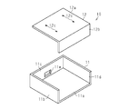
- the lower case 11 includes a rectangular plate-like base plate 11a and side plates 11b, 11c, and 11d that are erected at the end of the base plate 11a.
- a through hole 11e is formed in the side plate 11c, and the external connector 13 shown in FIG. 1 is attached to the through hole 11e.
- the upper case 12 has an upper plate 12a and a side plate 12b, and can be a substantially L-shaped cover.
- the upper case 12 is attached to the lower case 11 by, for example, snap fitting, and defines an internal space of the module case 10.
- a circuit board 20 is attached to the base plate 11 a of the lower case 11.
- the circuit board 20 is supported by being separated from the base plate 11a by a support 25 between the lower case 11 and the base plate 11a, and is fixed to the lower case 11 by screws 26 as fixing members.
- the length of the column 25, that is, the distance between the base plate 11 a of the lower case 11 and the circuit board 20 is set according to the electronic components mounted on the circuit board 20.
- the lead 13a of the external connector 13 is connected to the circuit board 20 by, for example, soldering.
- a plurality of electronic components 21 a and 21 b are mounted on the circuit board 20.
- the electronic components 21 a and 21 b constitute a control circuit that controls the charging current and discharging current for the capacitor 30.
- the electronic component 21a mounted on the upper surface of the circuit board 20 (sometimes referred to as a capacitor side mounting surface) is a macro computer, a logic IC, a small signal system transistor, or the like. These electronic components 21a consume less power and generate little heat.
- the electronic component 21b mounted on the lower surface of the circuit board 20 (sometimes referred to as a lower case side mounting surface) is a switch element such as a MOS transistor, an element constituting a snubber circuit, a rectifier diode, or a bypass capacitor. These electronic components 21b generate a large amount of heat.
- a housing case 40 is fixed to the lower surface of the upper plate 12 a, and a plurality of capacitors 30 are housed in the housing case 40. As shown in FIG. 3, four capacitors 30 are accommodated in the accommodation case 40.
- the capacitor 30 has a capacitor body 31 and a pair of lead wires 32.
- Capacitor body 31 is formed, for example, in a columnar shape and accommodates a power storage element.
- the storage case 40 is formed in a substantially rectangular parallelepiped shape.
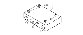
- a plurality (four in FIG. 4) of locking portions 41 are formed to protrude from the upper surface 40a of the housing case 40.
- a plurality of (four in FIG. 5) insertion holes 12 c are formed in the upper plate 12 a of the upper case 12.
- locking part 41 of the storage case 40 is inserted in the insertion hole 12c of the upper case 12 (upper board 12a).
- the locking portion 41 is, for example, a snap fit, engages with the upper plate 12a, and fixes the housing case 40 to the upper case 12 (upper plate 12a).
- the storage case 40 that stores the capacitor 30 is integrated with the upper case 12 (upper plate 12a).
- a plurality of (four) accommodation holes 42 corresponding to the number of capacitors 30 to be accommodated are formed in the accommodation case 40.
- the accommodation hole 42 is formed in a cylindrical shape according to the shape of the capacitor body 31 and holds the inserted capacitor body 31.
- a capacitor corresponding to one accommodation hole 42 is omitted.
- the housing case 40 has ribs (not shown) arranged along the circumferential direction on the inner surface of the housing hole 42. The rib is formed so as to extend along the insertion direction of the capacitor 30.
- the diameter of the circle connecting the apexes of the plurality of ribs is set to be slightly smaller than the diameter of the capacitor body 31. Therefore, the capacitor body 31 inserted into the accommodation hole 42 is held by the accommodation case 40.
- the lead wire 32 of the capacitor 30 is led out from the circular end surface of the capacitor body 31 in a direction perpendicular to the end surface. Further, the pair of lead wires 32 are bent and formed in an L shape in side view so as to extend toward the circuit board 20.
- the lead wire 32 is supported by a mounting portion 14 formed on the inner side surface 12 d of the side plate 12 b of the upper case 12 and a terminal holding plate 15 fixed to the mounting portion 14.
- the terminal holding plate 15 has a slit 15a into which the lead wire 32 is inserted.
- the terminal holding plate 15 in which the lead wire 32 is inserted into the slit 15a is fixed to the attachment portion 14 by, for example, snap fitting.
- the terminal holding plate 15 may be fixed to the attachment portion 14 with, for example, an adhesive, welding, screws, or the like.
- connection hole 22 is a conductive through hole in which a conductor such as plating is formed on the inner surface, and electrically connects the pattern on the circuit board 20 and the lead wire 32.
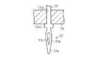
- the lead wire 32 has a press-fit terminal 33 at its tip.
- the press-fit terminal 33 has a guide portion 33a, a press-fit portion 33b, and an attachment portion 33d in order from the tip.
- the guide portion 33a is formed in a tapered shape (tapered shape) with a thin tip. The guide portion 33a facilitates insertion of the lead wire 32 into the connection hole 22 of the circuit board 20 shown in FIG.
- the press-fit portion 33b protrudes in a direction orthogonal to the length direction (vertical direction in FIG. 6).
- the width of the press-fit portion 33b is larger than the inner diameter of the connection hole 22 of the circuit board 20 shown in FIG.
- a window 33c extending in the length direction is formed at the center of the press-fit portion 33b.
- the window portion 33c enables deformation in which the press-fit portion 33b is elastically reduced in diameter.
- the mounting portion 33d protrudes outward on both sides along a direction orthogonal to the direction in which the press-fit terminal 33 extends (the axial direction of the press-fit terminal 33 and the vertical direction in FIG. 6).
- the attachment portion 33d is formed in a rectangular shape, for example.
- the attachment portion 33d engages with the terminal holding plate 15, and press-fits the press-fit portion 33b of the press-fit terminal 33 at the time of connection into the connection hole 22 (see FIG. 2).
- the housing case 40 that houses the capacitor 30 is fixed to the upper case 12 of the module case 10.
- the circuit board 20 to which the capacitor 30 is connected is fixed to the lower case 11 of the module case 10. Therefore, since the circuit board 20 and the housing case 40 are separated from each other, the electronic component 21a is mounted in a region where the circuit board 20 and the housing case 40 overlap in a plan view. Therefore, the area of the circuit board 20 on which the electronic component 21a is mounted can be reduced.
- the area of the module case 10 that accommodates the circuit board 20, that is, the area necessary for fixing the capacitor module can be reduced.
- the capacitor 30 is housed in the housing case 40 fixed to the upper plate 12a of the upper case 12.
- the terminal of the capacitor 30 is fixed to the side plate 12b extending from the upper plate 12a in the direction orthogonal to the upper plate 12a. For this reason, the relative movement of the lead wire 32 of the capacitor 30 with respect to the upper case 12 is prevented or reduced. Relative movement of the lead wire 32 of the capacitor 30 causes disconnection of the lead wire 32 and poor connection with the circuit board. For this reason, generation
- the capacitor 30 held in the upper case 12 has a capacitor body 31 housed in the housing case 40 and lead wires 32 protruding from the capacitor body 31.
- the lead wire 32 is electrically connected to the connection hole 22 formed in the circuit board 20.
- a charging current and a discharging current for the capacitor 30 are controlled by a control circuit configured by the electronic components 21 a and 21 b mounted on the circuit board 20.
- the lead wire 32 has a press-fit terminal 33 at its tip, and the press-fit terminal 33 is press-fitted into the connection hole 22 of the circuit board 20, and the capacitor 30 is easily connected to the circuit board 20.
- the press-fit terminal 33 has a mounting portion 33d, and the terminal holding plate 15 fixed to the upper case 12 is disposed closer to the capacitor body 31 than the mounting portion 33d.
- the terminal holding plate 15 engages with the attachment portion 33 d to restrict the movement of the press fit terminal 33, so that the press fit terminal 33 is press-fitted into the connection hole 22.
- the electronic components 21a and 21b are mounted on both surfaces of the circuit board 20, and the electronic component 21b having a large heat generation amount is mounted on the surface on the lower case 11 side. For this reason, the heat of the electronic component 21b is not easily transmitted to the capacitor 30, and the temperature rise of the capacitor 30 is suppressed.
- the capacitor module has a module case 10 including a lower case 11 and an upper case 12.
- a storage case 40 is fixed to the inner surface of the upper case 12, and the capacitor 30 is stored in the storage case 40.
- a circuit board 20 is fixed to the upper surface of the lower case 11.
- the circuit board 20 has a wiring electrically connected to the capacitor 30, and is mounted with electronic components 21 a and 21 b that constitute a circuit that controls a current to the capacitor 30.
- the circuit board 20 is connected to a device outside the module (for example, a brake control device or the like) via an external connection connector 13 fixed to the lower case 11.
- the housing case 40 that houses the capacitor 30 is fixed to the upper case 12 of the module case 10.
- the circuit board 20 to which the capacitor 30 is connected is fixed to the lower case 11 of the module case 10. Therefore, since the circuit board 20 and the housing case 40 are separated from each other, the electronic component 21a is mounted in a region where the circuit board 20 and the housing case 40 overlap in a plan view, and the circuit board 20 and the module case 10 are downsized. Can do.
- the area of the module case 10 that accommodates the circuit board 20, that is, the area necessary for fixing the capacitor module can be reduced.
- the capacitor 30 is housed in the housing case 40 fixed to the upper plate of the upper case 12.
- the terminal of the capacitor 30 is fixed to a side plate extending from the upper plate in a direction orthogonal to the upper plate. For this reason, the terminal of the capacitor 30 becomes difficult to move relative to the upper case 12.
- the relative movement of the lead wire 32 causes disconnection of the lead wire 32 and poor connection with the circuit board. For this reason, generation
- the capacitor 30 held in the upper case 12 has a capacitor body 31 housed in the housing case 40 and a lead wire protruding from the capacitor body 31.
- the lead wire is electrically connected to a connection hole formed in the circuit board 20.
- a charging circuit and a discharging current for the capacitor 30 can be controlled by a control circuit configured by the electronic components 21 a and 21 b mounted on the circuit board 20.
- the lead wire 32 has a press-fit terminal at its tip, and the press-fit terminal is press-fitted into the connection hole of the circuit board 20. Therefore, the capacitor 30 can be easily connected to the circuit board 20.
- the capacitor 30 is connected to the circuit board 20 when the lower case 11 and the upper case 12 are assembled. That is, since the upper case 12 is assembled to the lower case 11 and the capacitor 30 is connected to the circuit board 20 at the same time, a process for connecting the capacitor 30 to the circuit board 20 is not required. Such time can be reduced.
- the press-fit terminal 33 has a mounting portion 33d, and the terminal holding plate 15 fixed to the upper case 12 is disposed closer to the capacitor body 31 than the mounting portion 33d.
- the terminal holding plate 15 engages with the attachment portion 33d to restrict the movement of the press fit terminal 33, so that the press fit terminal 33 can be surely press-fitted into the connection hole 22.
- the electronic components 21a and 21b are mounted on both surfaces of the circuit board 20, and the electronic component 21b having a large heat generation amount is mounted on the surface on the lower case 11 side. For this reason, the heat of the electronic component 21b is not easily transmitted to the capacitor 30, and the temperature rise of the capacitor 30 can be suppressed. The increase in temperature of the capacitor 30 decreases the characteristics and life. Therefore, by mounting the electronic component 21b in this way, it is possible to suppress the performance degradation of the capacitor 30 and to extend the life.
- the housing case 40 and the circuit board 20 are arranged between the top plate and the bottom plate of the module case 10 (that is, between the upper plate 12a of the upper case 12 and the base plate 11a of the lower case 11).
- the housing case 40 and the circuit board 20 face each other with an empty space between them.
- At least one electronic component 21a mounted on the circuit board 20 faces the housing case 40 in the empty space (see FIG. 1). According to this configuration, the footprint of the circuit board 20 can be reduced, and the module case 10 can be reduced in size.
- the number of capacitors 30 is four, but may be appropriately changed to three or less or five or more.
- the housing case 40 is integrally fixed to the upper case 12 by the locking portion 41 of the upper surface 40a of the housing case 40, but the method of fixing the housing case 40 is not limited to this method.
- the engaging part of the side plate 12b of the upper case 12 and the engaging part on the side surface of the housing case 40 may be fixed by snap fitting.
- the housing case 40 may be fixed to the upper case 12 with screws (bolts and nuts) or the like.
- the housing case 40 is not limited to the case 11 or 12 having the illustrated shape, and may be divided in various ways.
- the storage cases 40 may be divided equally or non-uniformly in the vertical direction of FIG.
Landscapes
- Engineering & Computer Science (AREA)
- Power Engineering (AREA)
- Microelectronics & Electronic Packaging (AREA)
- Manufacturing & Machinery (AREA)
- Electric Double-Layer Capacitors Or The Like (AREA)
- Structures For Mounting Electric Components On Printed Circuit Boards (AREA)
- Details Of Connecting Devices For Male And Female Coupling (AREA)
Abstract
キャパシタモジュールは、下部ケース11と上部ケース12とからなるモジュールケース10を有する。上部ケース12の内側面に収容ケース40が固定され、その収容ケース40にキャパシタ30が収容される。下部ケース11の上面に回路基板20が固定されている。回路基板20は、キャパシタ30に電気的に接続される配線を有し、キャパシタ30に対する電流を制御する回路を構成する電子部品21a,21bが実装されている。
Description
本発明は、キャパシタモジュールに関する。
従来、車両に搭載された各種の負荷装置は、バッテリから供給される電力に基づいて動作する。バッテリの故障あるいは電圧低下などによる電源失陥時には、各負荷装置の動作が保障されない。このため、大容量キャパシタ等の蓄電部材を有するバックアップ用の電源装置が提案されている。大容量キャパシタは、回路基板に固定されたケースに収容され、その回路基板に実装される(たとえば、特許文献1参照)。
ところで、回路基板には、各種の電子部品が搭載される。しかしながら、上記のように、大容量キャパシタを収容するケースを回路基板上に固定すると、ケースにより電子部品の配置が制約される。このような配置の制約は、回路基板の大型化、ひいては回路基板を収容するモジュールの大型化を招く。
本発明の目的は、キャパシタモジュールを小型化することにある。
本発明の一局面に従うキャパシタモジュールは、下部ケースと上部ケースとからなるモジュールケースと、前記上部ケースの内側面に固定された収容ケースと、前記収容ケースに収容されたキャパシタと、前記下部ケースの上面に固定され、前記キャパシタに電気的に接続される配線を有し、前記キャパシタに対する電流を制御する回路を構成する電子部品が実装された回路基板と、前記下部ケースに固定され、前記回路基板の配線に接続された端子を含む外部接続コネクタとを有する。
本発明の一局面に従うキャパシタモジュールは、下部ケースと上部ケースとからなるモジュールケースと、前記上部ケースの内側面に固定された収容ケースと、前記収容ケースに収容されたキャパシタと、前記下部ケースの上面に固定され、前記キャパシタに電気的に接続される配線を有し、前記キャパシタに対する電流を制御する回路を構成する電子部品が実装された回路基板と、前記下部ケースに固定され、前記回路基板の配線に接続された端子を含む外部接続コネクタとを有する。
この構成によれば、キャパシタを収容する収容ケースはモジュールケースの上部ケースに固定される。そして、キャパシタが接続される回路基板は、モジュールケースの下部ケースに固定される。したがって、回路基板と収容ケースとが互いに離間するため、平面視において回路基板と収容ケースとが重なる領域に電子部品が実装され、回路基板とモジュールケースを小型化することができる。
上記のキャパシタモジュールにおいて、前記上部ケースは、前記収容ケースを固定的に支持する上板と、前記上板の端部から前記上板に対して直交方向に延びる側板と、前記側板に固定され、前記キャパシタの端子を保持する端子保持板とを有することが好ましい。
この構成によれば、上部ケースの上板に固定した収容ケースにキャパシタが収容される。そのキャパシタの端子は、上板からその上板の直交方向に延びる側板に固定される。このため、キャパシタの端子は上部ケースに対して相対的に移動し難くなる。
上記のキャパシタモジュールにおいて、前記キャパシタは、前記収容ケースに収容されるキャパシタ本体と、前記キャパシタ本体から突出するリード線とを有し、前記回路基板は、前記キャパシタのリード線が電気的に接続される接続孔を有することが好ましい。
この構成によれば、上部ケースに保持されたキャパシタは、収容ケースに収容されるキャパシタ本体と、そのキャパシタ本体から突出するリード線とを有している。リード線は、回路基板に形成された接続孔に電気的に接続される。
上記のキャパシタモジュールは、前記キャパシタのリード線は、その先端に前記接続孔の内径より幅広であって弾性変形可能な圧入部を有するプレスフィット端子を有し、前記プレスフィット端子の前記圧入部が前記回路基板の前記接続孔に圧入されていることが好ましい。
この構成によれば、リード線はその先端にプレスフィット端子を有し、そのプレスフィット端子が回路基板の接続孔に圧入され、回路基板に対してキャパシタが容易に接続される。
上記のキャパシタモジュールは、前記プレスフィット端子は、前記リード線に対して直交する方向に突出する取付部を有し、前記端子保持板は、前記取付部より前記キャパシタ本体側に配置されて前記プレスフィット端子を保持することが好ましい。
この構成によれば、プレスフィット端子は取付部を有し、上部ケースに固定された端子保持板は取付部よりキャパシタ本体側に配置される。この端子保持板が取付部と係合することで、プレスフィット端子が接続孔に圧入される。
上記のキャパシタモジュールにおいて、前記電子部品は前記回路基板の下部ケース側実装面に実装された電子部品と、前記回路基板において前記下部ケース側実装面の反対側のキャパシタ側実装面に実装された電子部品とを含み、前記下部ケース側実装面に実装された前記電子部品の発熱量が、前記キャパシタ側実装面に実装された前記電子部品の発熱量より大きいことが好ましい。
この構成によれば、回路基板の両面に電子部品が実装され、発熱量の大きい電子部品が下部ケースの側の面に実装される。このため、電子部品の熱がキャパシタに伝わり難く、キャパシタの温度上昇が抑制される。
上記のキャパシタモジュールにおいて、前記収容ケースと前記回路基板とは、それらの間に空きスペースをおいて対面し、前記電子部品のうちの少なくとも一つが前記空きスペースにおいて前記収容ケースと対面していることが好ましい。
この構成によれば、回路基板のフットプリントを小さくすることができ、モジュールケースを小型化することができる。
本発明によれば、キャパシタモジュールを小型化することができる。
本発明によれば、キャパシタモジュールを小型化することができる。
以下、実施形態のキャパシタモジュールを説明する。なお、添付図面は、理解を容易にするために構成要素を拡大して示している場合がある。構成要素の寸法比率は実際のものと、または別の図面中のものと異なる場合がある。
図1に示すように、キャパシタモジュールは、モジュールケース10と、このモジュールケース10に収容された回路基板20及び複数のキャパシタ30を備えている。キャパシタ30は、たとえば電気二重層キャパシタである。
モジュールケース10は略直方体状に形成されている。モジュールケース10は、たとえば合成樹脂製である。モジュールケース10は、車両に取り付けるための図示しない取付部を含むことができる。
モジュールケース10は、下部ケース11と、その下部ケース11に対して取着される上部ケース12とを備えている。図5に示すように、下部ケース11は、矩形板状のベース板11aと、そのベース板11aの端部に立設された側板11b,11c,11dを有している。側板11cには貫通孔11eが形成され、その貫通孔11eに図1に示す外部接続コネクタ13が取着される。
上部ケース12は、上板12aと側板12bとを有しており、略L字状のカバーであり得る。この上部ケース12は、下部ケース11にたとえばスナップフィットにより取着され、モジュールケース10の内部空間を画定する。
図2に示すように、下部ケース11のベース板11aには、回路基板20が取着されている。回路基板20は、下部ケース11のベース板11aとの間の支柱25によりベース板11aから離間して支持され、固定部材としてのネジ26により下部ケース11に固定されている。支柱25の長さ、つまり下部ケース11のベース板11aと回路基板20との間の距離は、回路基板20に実装される電子部品に応じて設定されている。
回路基板20には、外部接続コネクタ13のリード13aがたとえば半田付けにより接続されている。
回路基板20には、複数の電子部品21a,21bが実装されている。電子部品21a,21bは、キャパシタ30に対する充電電流,放電電流を制御する制御回路を構成する。
回路基板20には、複数の電子部品21a,21bが実装されている。電子部品21a,21bは、キャパシタ30に対する充電電流,放電電流を制御する制御回路を構成する。
回路基板20の上面(キャパシタ側実装面と呼ぶことがある)に実装された電子部品21aは、マクロコンピュータ、ロジックIC、小信号系のトランジスタ、等である。これらの電子部品21aは、消費電力が少なく、発熱の小さなものである。
回路基板20の下面(下部ケース側実装面と呼ぶことがある)に実装された電子部品21bは、MOSトランジスタ等のスイッチ素子、スナバ回路を構成する素子、整流ダイオード、バイパスコンデンサなどである。これらの電子部品21bは、発熱の大きなものである。
上部ケース12において、上板12aの下面には、収容ケース40が固定され、その収容ケース40に複数のキャパシタ30が収容されている。
図3に示すように、収容ケース40には4個のキャパシタ30が収容されている。
図3に示すように、収容ケース40には4個のキャパシタ30が収容されている。
キャパシタ30は、キャパシタ本体31と一対のリード線32とを有している。キャパシタ本体31は、たとえば円柱状に形成され、蓄電要素を収容する。
図4に示すように、収容ケース40は略直方体状に形成されている。収容ケース40の上面40aには複数(図4では4個)の係止部41が突出形成されている。図5に示すように、上部ケース12の上板12aには、対応する複数(図5では4個)の挿通孔12cが形成されている。図1に示すように、収容ケース40の係止部41を上部ケース12(上板12a)の挿通孔12cに挿入させる。係止部41はたとえばスナップフィットであり、上板12aと係合し、収容ケース40を上部ケース12(上板12a)に固定する。このように、キャパシタ30を収容した収容ケース40は、上部ケース12(上板12a)と一体化される。
図4に示すように、収容ケース40は略直方体状に形成されている。収容ケース40の上面40aには複数(図4では4個)の係止部41が突出形成されている。図5に示すように、上部ケース12の上板12aには、対応する複数(図5では4個)の挿通孔12cが形成されている。図1に示すように、収容ケース40の係止部41を上部ケース12(上板12a)の挿通孔12cに挿入させる。係止部41はたとえばスナップフィットであり、上板12aと係合し、収容ケース40を上部ケース12(上板12a)に固定する。このように、キャパシタ30を収容した収容ケース40は、上部ケース12(上板12a)と一体化される。
図3に示すように、収容ケース40には、収容するキャパシタ30の数に応じた複数(4個)の収容孔42が形成されている。
図4に示すように、収容孔42は、キャパシタ本体31の形状に応じて円筒状に形成され、内挿されたキャパシタ本体31を保持する。図では、1つの収容孔42に対応するキャパシタを省略している。たとえば、収容ケース40は、収容孔42の内面に、周方向に沿って配列されたリブ(図示略)を有している。リブは、キャパシタ30の挿入方向に沿って延びるように形成されている。複数のリブの頂点を結ぶ円の直径は、キャパシタ本体31の直径よりも僅かに小さく設定されている。したがって、収容孔42に挿入されたキャパシタ本体31は、収容ケース40により保持される。
図4に示すように、収容孔42は、キャパシタ本体31の形状に応じて円筒状に形成され、内挿されたキャパシタ本体31を保持する。図では、1つの収容孔42に対応するキャパシタを省略している。たとえば、収容ケース40は、収容孔42の内面に、周方向に沿って配列されたリブ(図示略)を有している。リブは、キャパシタ30の挿入方向に沿って延びるように形成されている。複数のリブの頂点を結ぶ円の直径は、キャパシタ本体31の直径よりも僅かに小さく設定されている。したがって、収容孔42に挿入されたキャパシタ本体31は、収容ケース40により保持される。
図2に示すように、キャパシタ30のリード線32は、キャパシタ本体31の円形状の端面からこの端面と直交する方向に導出されている。さらに、一対のリード線32は、回路基板20に向かって延びるように、側面視L字状に屈曲形成されている。そのリード線32は、上部ケース12の側板12bの内側面12dに形成された取着部14と、その取着部14に固定された端子保持板15とにより支持されている。
図3に示すように、端子保持板15には、リード線32が挿入されるスリット15aが形成されている。そのスリット15aにリード線32を挿入した端子保持板15は、取着部14にたとえばスナップフィットにより固定されている。なお、端子保持板15は、たとえば接着剤、溶着、ネジ等によって取着部14に固定されてもよい。
図2に示すように、回路基板20には、複数のキャパシタ30の一対のリード線32をそれぞれ接続する接続孔22が形成されている。接続孔22はメッキ等の導体が内面に形成されて導電性を有するスルーホールであり、回路基板20上のパターンとリード線32とを電気的に接続する。
図6に示すように、リード線32はその先端にプレスフィット端子33を有している。プレスフィット端子33は、先端から順に、案内部33a、圧入部33b、取付部33dを有している。案内部33aは先端が細い先細り状(テーパ状)に形成されている。案内部33aは、図2に示す回路基板20の接続孔22へのリード線32の挿入を容易にする。
圧入部33bは、長さ方向(図6の上下方向)と直交する方向へ張り出している。圧入部33bの幅は、図2に示す回路基板20の接続孔22の内径よりも大きい。圧入部33bの中央には、長さ方向に延びる窓部33cが形成されている。窓部33cは、圧入部33bが弾性的に縮径する変形を可能とする。
取付部33dは、プレスフィット端子33の延びる方向(プレスフィット端子33の軸線方向であって、図6の上下方向)と直交する方向に沿って両側外方へ突出している。取付部33dは、たとえば矩形状に形成されている。取付部33dは、端子保持板15と係合し、接続時におけるプレスフィット端子33の圧入部33bを接続孔22(図2参照)へ圧入する。
次に、上記のキャパシタモジュールの作用を説明する。
図1に示すように、キャパシタ30を収容する収容ケース40はモジュールケース10の上部ケース12に固定される。そして、キャパシタ30が接続される回路基板20は、モジュールケース10の下部ケース11に固定される。したがって、回路基板20と収容ケース40とが互いに離間するため、平面視において回路基板20と収容ケース40とが重なる領域に電子部品21aが実装される。したがって、電子部品21aが実装される回路基板20の面積を縮小することができる。そして、この回路基板20を収容するモジュールケース10、つまりキャパシタモジュールの固定に必要な領域の面積の縮小を図ることができる。
図1に示すように、キャパシタ30を収容する収容ケース40はモジュールケース10の上部ケース12に固定される。そして、キャパシタ30が接続される回路基板20は、モジュールケース10の下部ケース11に固定される。したがって、回路基板20と収容ケース40とが互いに離間するため、平面視において回路基板20と収容ケース40とが重なる領域に電子部品21aが実装される。したがって、電子部品21aが実装される回路基板20の面積を縮小することができる。そして、この回路基板20を収容するモジュールケース10、つまりキャパシタモジュールの固定に必要な領域の面積の縮小を図ることができる。
上部ケース12の上板12aに固定した収容ケース40にキャパシタ30が収容される。そのキャパシタ30の端子は、上板12aからその上板12aの直交方向に延びる側板12bに固定される。このため、上部ケース12に対するキャパシタ30のリード線32の相対的な移動が防止または低減される。キャパシタ30のリード線32の相対的な移動は、リード線32の断線や回路基板との接続不良の要因となる。このため、リード線32の相対的な移動を抑制することで、不良の発生が抑制される。
上部ケース12に保持されたキャパシタ30は、収容ケース40に収容されるキャパシタ本体31と、そのキャパシタ本体31から突出するリード線32とを有している。リード線32は、回路基板20に形成された接続孔22に電気的に接続される。回路基板20に実装された電子部品21a,21bにより構成される制御回路により、キャパシタ30に対する充電電流と放電電流が制御される。
リード線32はその先端にプレスフィット端子33を有し、そのプレスフィット端子33が回路基板20の接続孔22に圧入され、回路基板20に対してキャパシタ30が容易に接続される。
プレスフィット端子33は取付部33dを有し、上部ケース12に固定された端子保持板15は取付部33dよりキャパシタ本体31側に配置される。この端子保持板15が取付部33dと係合してプレスフィット端子33の移動を制限することで、プレスフィット端子33が接続孔22に圧入される。
回路基板20の両面に電子部品21a,21bが実装され、発熱量の大きい電子部品21bが下部ケース11の側の面に実装される。このため、電子部品21bの熱がキャパシタ30に伝わり難く、キャパシタ30の温度上昇が抑制される。
以上記述したように、本実施形態によれば、以下の効果を奏する。
(1)キャパシタモジュールは、下部ケース11と上部ケース12とからなるモジュールケース10を有する。上部ケース12の内側面に収容ケース40が固定され、その収容ケース40にキャパシタ30が収容される。下部ケース11の上面に回路基板20が固定されている。回路基板20は、キャパシタ30に電気的に接続される配線を有し、キャパシタ30に対する電流を制御する回路を構成する電子部品21a,21bが実装されている。また、回路基板20は、下部ケース11に固定された外部接続コネクタ13を介してモジュール外部の装置(たとえば、ブレーキ制御装置等)に接続される。
(1)キャパシタモジュールは、下部ケース11と上部ケース12とからなるモジュールケース10を有する。上部ケース12の内側面に収容ケース40が固定され、その収容ケース40にキャパシタ30が収容される。下部ケース11の上面に回路基板20が固定されている。回路基板20は、キャパシタ30に電気的に接続される配線を有し、キャパシタ30に対する電流を制御する回路を構成する電子部品21a,21bが実装されている。また、回路基板20は、下部ケース11に固定された外部接続コネクタ13を介してモジュール外部の装置(たとえば、ブレーキ制御装置等)に接続される。
キャパシタ30を収容する収容ケース40はモジュールケース10の上部ケース12に固定される。そして、キャパシタ30が接続される回路基板20は、モジュールケース10の下部ケース11に固定される。したがって、回路基板20と収容ケース40とが互いに離間するため、平面視において回路基板20と収容ケース40とが重なる領域に電子部品21aが実装され、回路基板20とモジュールケース10を小型化することができる。そして、この回路基板20を収容するモジュールケース10、つまりキャパシタモジュールの固定に必要な領域の面積の縮小を図ることができる。
(2)上部ケース12の上板に固定した収容ケース40にキャパシタ30が収容される。そのキャパシタ30の端子は、上板からその上板の直交方向に延びる側板に固定される。このため、キャパシタ30の端子は上部ケース12に対して相対的に移動し難くなる。キャパシタ30において、リード線32の相対的な移動は、リード線32の断線や回路基板との接続不良の要因となる。このため、リード線32の相対的な移動を抑制することで、不良の発生を抑制することができる。
(3)上部ケース12に保持されたキャパシタ30は、収容ケース40に収容されるキャパシタ本体31と、そのキャパシタ本体31から突出するリード線とを有している。リード線は、回路基板20に形成された接続孔に電気的に接続される。回路基板20に実装された電子部品21a,21bにより構成される制御回路により、キャパシタ30に対する充電電流と放電電流を制御することができる。
(4)リード線32はその先端にプレスフィット端子を有し、そのプレスフィット端子が回路基板20の接続孔に圧入されている。したがって、回路基板20に対してキャパシタ30を容易に接続することができる。この回路基板20に対するキャパシタ30の接続は、下部ケース11と上部ケース12との組み付けの際に行われる。つまり、下部ケース11に対して上部ケース12を組み付けと同時に、回路基板20に対してキャパシタ30を接続するため、キャパシタ30を回路基板20に接続するための工程が不要となり、製造工数や製造に係る時間等を低減することができる。
(5)プレスフィット端子33は取付部33dを有し、上部ケース12に固定された端子保持板15は取付部33dよりキャパシタ本体31側に配置される。この端子保持板15が取付部33dと係合してプレスフィット端子33の移動を制限することで、プレスフィット端子33を接続孔22に確実に圧入することができる。
(6)回路基板20の両面に電子部品21a,21bが実装され、発熱量の大きい電子部品21bが下部ケース11の側の面に実装される。このため、電子部品21bの熱がキャパシタ30に伝わり難く、キャパシタ30の温度上昇を抑制することができる。キャパシタ30の温度上昇は、特性や寿命を低下させる。したがって、このように電子部品21bを実装することで、キャパシタ30の性能低下を抑制し、長寿命化を図ることができる。
(7)収容ケース40及び回路基板20は、モジュールケース10の天板と底板との間(すなわち上部ケース12の上板12aと下部ケース11のベース板11aとの間)に配置されている。収容ケース40と回路基板20とは、それらの間に空きスペース(empty space)をおいて対面している。回路基板20に搭載された少なくとも一つの電子部品21aがその空きスペースにおいて収容ケース40に対面している(図1参照)。この構成によれば、回路基板20のフットプリントを小さくすることができ、モジュールケース10を小型化することができる。
尚、実施形態は、以下の様に変更してもよい。
・上記実施形態では、キャパシタ30は4個としたが、3個以下または5個以上に適宜変更してもよい。
・上記実施形態では、キャパシタ30は4個としたが、3個以下または5個以上に適宜変更してもよい。
・上記実施形態では、収容ケース40の上面40aの係止部41により収容ケース40を上部ケース12に一体的に固定したが、収容ケース40の固定方法はこの方法に限定されない。上部ケース12のたとえば側板12bの係止部と、収容ケース40の側面の係合部とをスナップフィットにより固定してもよい。または、ネジ(ボルトとナット)等により収容ケース40を上部ケース12に固定してもよい。
・収容ケース40は図示した形状のケース11、12に分割されるものに限定されず、様々な様式で分割されてもよい。たとえば図1の上下方向に収容ケース40が均等に又は不均等に分割されてもよい。
本発明は、例示したものに限定されるものではない。例えば、例示した特徴が本発明にとって必須であると解釈されるべきでなく、本発明の主題は、開示した特定の実施形態の全ての特徴より少ない特徴に存在することがある。
10…モジュールケース、11…下部ケース、12…上部ケース、12a…上板、12b…側板、14…取付部、15…端子保持板、20…回路基板、21a,21b…電子部品、22…接続孔、30…キャパシタ、31…キャパシタ本体、32…リード線、33…プレスフィット端子、40…収容ケース、42…収容孔。
Claims (7)
- 下部ケースと上部ケースとからなるモジュールケースと、
前記上部ケースの内側面に固定された収容ケースと、
前記収容ケースに収容されたキャパシタと、
前記下部ケースの上面に固定され、前記キャパシタに電気的に接続される配線を有し、前記キャパシタに対する電流を制御する回路を構成する電子部品が実装された回路基板と、
前記下部ケースに固定され、前記回路基板の配線に接続された端子を含む外部接続コネクタと、
を有することを特徴とするキャパシタモジュール。 - 請求項1に記載のキャパシタモジュールにおいて、
前記上部ケースは、
前記収容ケースを固定的に支持する上板と、
前記上板の端部から前記上板に対して直交方向に延びる側板と、
前記側板に固定され、前記キャパシタの端子を保持する端子保持板と
を有することを特徴とするキャパシタモジュール。 - 請求項2に記載のキャパシタモジュールにおいて、
前記キャパシタは、前記収容ケースに収容されるキャパシタ本体と、前記キャパシタ本体から突出するリード線とを有し、
前記回路基板は、前記キャパシタのリード線が電気的に接続される接続孔を有することを特徴とするキャパシタモジュール。 - 請求項3に記載のキャパシタモジュールにおいて、
前記キャパシタのリード線は、その先端に前記接続孔の内径より幅広であって弾性変形可能な圧入部を有するプレスフィット端子を有し、
前記プレスフィット端子の前記圧入部が前記回路基板の前記接続孔に圧入されていることを特徴とするキャパシタモジュール。 - 請求項4に記載のキャパシタモジュールにおいて、
前記プレスフィット端子は、前記リード線に対して直交する方向に突出する取付部を有し、
前記端子保持板は、前記取付部より前記キャパシタ本体側に配置されて前記プレスフィット端子を保持することを特徴とするキャパシタモジュール。 - 請求項1~5のいずれか一項に記載のキャパシタモジュールにおいて、
前記電子部品は、前記回路基板の下部ケース側実装面に実装された電子部品と、前記回路基板において前記下部ケース側実装面の反対側のキャパシタ側実装面に実装された電子部品とを含み、
前記下部ケース側実装に実装された前記電子部品の発熱量が、前記キャパシタ側実装面に実装された前記電子部品の発熱量より大きいことを特徴とするキャパシタモジュール。 - 請求項1~6のいずれか一項に記載のキャパシタモジュールにおいて、前記収容ケースと前記回路基板とは、それらの間に空きスペースをおいて対面し、前記電子部品のうちの少なくとも一つが前記空きスペースにおいて前記収容ケースと対面していることを特徴とするキャパシタモジュール。
Priority Applications (2)
| Application Number | Priority Date | Filing Date | Title |
|---|---|---|---|
| CN201580071054.XA CN107112141B (zh) | 2015-01-08 | 2015-12-21 | 电容器模块 |
| US15/541,779 US20170352495A1 (en) | 2015-01-08 | 2015-12-21 | Capacitor module |
Applications Claiming Priority (2)
| Application Number | Priority Date | Filing Date | Title |
|---|---|---|---|
| JP2015002101A JP6421601B2 (ja) | 2015-01-08 | 2015-01-08 | キャパシタモジュール |
| JP2015-002101 | 2015-01-08 |
Publications (1)
| Publication Number | Publication Date |
|---|---|
| WO2016111154A1 true WO2016111154A1 (ja) | 2016-07-14 |
Family
ID=56355854
Family Applications (1)
| Application Number | Title | Priority Date | Filing Date |
|---|---|---|---|
| PCT/JP2015/085650 Ceased WO2016111154A1 (ja) | 2015-01-08 | 2015-12-21 | キャパシタモジュール |
Country Status (4)
| Country | Link |
|---|---|
| US (1) | US20170352495A1 (ja) |
| JP (1) | JP6421601B2 (ja) |
| CN (1) | CN107112141B (ja) |
| WO (1) | WO2016111154A1 (ja) |
Families Citing this family (8)
| Publication number | Priority date | Publication date | Assignee | Title |
|---|---|---|---|---|
| JP7336637B2 (ja) * | 2018-05-25 | 2023-09-01 | パナソニックIpマネジメント株式会社 | コンデンサ |
| EP3982384B1 (en) * | 2020-10-06 | 2023-07-26 | Veoneer Passive Co. AB | Electronic control unit |
| CN112768228B (zh) * | 2020-12-18 | 2023-04-07 | 东佳电子(郴州)有限公司 | 一种具有断电保护功能的电容器 |
| JP7491242B2 (ja) * | 2021-03-09 | 2024-05-28 | 住友電装株式会社 | 電子機器 |
| JPWO2022202579A1 (ja) * | 2021-03-25 | 2022-09-29 | ||
| US11839035B2 (en) * | 2021-12-20 | 2023-12-05 | Veoneer Us Safety Systems, Llc | Electronic control unit housing with electronic component holder |
| US11804336B2 (en) * | 2022-03-11 | 2023-10-31 | General Electric Company | Ultracapacitor module with integrated bypass diode and related systems |
| EP4312240B1 (en) * | 2022-07-27 | 2026-04-15 | Veoneer Sweden Safety Systems AB | Mounting structure for a capacitor in a housing part of a housing |
Citations (4)
| Publication number | Priority date | Publication date | Assignee | Title |
|---|---|---|---|---|
| JP2000152662A (ja) * | 1998-11-04 | 2000-05-30 | Denso Corp | 電源平滑用コンデンサ搭載型インバータ装置 |
| JP2000340920A (ja) * | 1999-05-31 | 2000-12-08 | Kyocera Corp | 回路基板および集積回路装置 |
| JP2003031449A (ja) * | 2001-07-11 | 2003-01-31 | Casio Comput Co Ltd | 蓄電構造およびそれを備えた電子機器 |
| JP2007281127A (ja) * | 2006-04-05 | 2007-10-25 | Shindengen Electric Mfg Co Ltd | コンデンサを備える回路装置及びコンデンサモジュール |
Family Cites Families (34)
| Publication number | Priority date | Publication date | Assignee | Title |
|---|---|---|---|---|
| US3087982A (en) * | 1959-12-01 | 1963-04-30 | Northrop Corp | Vacuum tube mounts |
| JPH0530381Y2 (ja) * | 1985-06-12 | 1993-08-03 | ||
| US5204498A (en) * | 1991-12-30 | 1993-04-20 | Therm-O-Disc, Incorporated | Packaging assembly |
| GB2353844B (en) * | 1996-08-29 | 2001-04-11 | Matsushita Electric Industrial Co Ltd | Vibrator holding device |
| DE59812848D1 (de) * | 1997-10-11 | 2005-07-14 | Conti Temic Microelectronic | Gehäuse zur Aufnahme elektronischer Bauelemente |
| DE19813639A1 (de) * | 1998-03-27 | 1999-11-25 | Danfoss As | Leistungsmodul für einen Stromrichter |
| CN1171255C (zh) * | 1998-09-16 | 2004-10-13 | 开利公司 | 电控制箱中电容器的安装装置 |
| US6354674B1 (en) * | 1998-12-11 | 2002-03-12 | Denso Corporation | Hydraulic control apparatus integrated with motor driving circuit unit |
| DE19857840C2 (de) * | 1998-12-15 | 2003-10-02 | Siemens Ag | Elektronische Einrichtung |
| DE19941690C2 (de) * | 1999-09-01 | 2001-12-06 | Siemens Ag | Steuergerät und Lötverfahren |
| DE10162600A1 (de) * | 2001-12-20 | 2003-07-10 | Bosch Gmbh Robert | Gehäuseanordnung für ein elektrisches Gerät |
| JP3864873B2 (ja) * | 2002-08-09 | 2007-01-10 | 株式会社デンソー | 電子制御装置 |
| US6717797B1 (en) * | 2002-11-22 | 2004-04-06 | Tyco Electronics Corporation | Apparatus, methods and articles of manufacture for a module box with integrated components |
| JP2005026270A (ja) * | 2003-06-30 | 2005-01-27 | Murata Mfg Co Ltd | 高圧用可変抵抗器 |
| EP1589547A4 (en) * | 2003-09-18 | 2009-11-25 | Panasonic Corp | CAPACITOR UNIT |
| ITTO20030754A1 (it) * | 2003-09-29 | 2005-03-30 | Gate Srl | Unita' elettronica di controllo, in particolare unita' |
| JP4859443B2 (ja) * | 2005-11-17 | 2012-01-25 | 日立オートモティブシステムズ株式会社 | 電力変換装置 |
| JP4853077B2 (ja) * | 2006-03-29 | 2012-01-11 | 株式会社豊田自動織機 | 電動コンプレッサ |
| DE112007000991B4 (de) * | 2006-04-27 | 2010-10-21 | Komatsu Ltd. | Kondensatormodul |
| US7903417B2 (en) * | 2006-10-10 | 2011-03-08 | Deere & Company | Electrical circuit assembly for high-power electronics |
| JP4751810B2 (ja) * | 2006-11-02 | 2011-08-17 | 日立オートモティブシステムズ株式会社 | 電力変換装置 |
| JP4702311B2 (ja) * | 2007-03-19 | 2011-06-15 | トヨタ自動車株式会社 | コンデンサを備えた電気ユニット |
| US8134343B2 (en) * | 2007-04-27 | 2012-03-13 | Flextronics International Kft | Energy storage device for starting engines of motor vehicles and other transportation systems |
| CN101802952A (zh) * | 2007-09-20 | 2010-08-11 | 松下电工株式会社 | 近程式传感器用的检测部及近程式传感器 |
| JP5095459B2 (ja) * | 2008-03-25 | 2012-12-12 | 株式会社小松製作所 | キャパシタモジュール |
| JP4638923B2 (ja) * | 2008-03-31 | 2011-02-23 | 日立オートモティブシステムズ株式会社 | 制御装置 |
| DE102008023714B4 (de) * | 2008-05-15 | 2011-01-20 | Semikron Elektronik Gmbh & Co. Kg | Anordnung mit einem Hauptträger und einer Leiterplatte mit Bauelementen |
| JP4657329B2 (ja) * | 2008-07-29 | 2011-03-23 | 日立オートモティブシステムズ株式会社 | 電力変換装置および電動車両 |
| JP5232047B2 (ja) * | 2009-03-10 | 2013-07-10 | 矢崎総業株式会社 | コンデンサの取り付け構造 |
| ITTO20100064U1 (it) * | 2010-04-13 | 2011-10-14 | Gate Srl | Unita' elettronica di controllo, in particolare unita' di controllo della velocita' di un elettroventilatore |
| US8149589B2 (en) * | 2010-08-19 | 2012-04-03 | Lien Chang Electronic Enterprise Co., Ltd. | Capacitor holder |
| CN202221699U (zh) * | 2011-08-16 | 2012-05-16 | 许文豪 | 一种电容固定装置及应用该电容固定装置的线路板结构 |
| JP5945710B2 (ja) * | 2011-10-28 | 2016-07-05 | パナソニックIpマネジメント株式会社 | キャパシタモジュール |
| US9974178B2 (en) * | 2014-09-11 | 2018-05-15 | Nsk Ltd. | Multipolar lead parts and board coupling device |
-
2015
- 2015-01-08 JP JP2015002101A patent/JP6421601B2/ja not_active Expired - Fee Related
- 2015-12-21 WO PCT/JP2015/085650 patent/WO2016111154A1/ja not_active Ceased
- 2015-12-21 CN CN201580071054.XA patent/CN107112141B/zh not_active Expired - Fee Related
- 2015-12-21 US US15/541,779 patent/US20170352495A1/en not_active Abandoned
Patent Citations (4)
| Publication number | Priority date | Publication date | Assignee | Title |
|---|---|---|---|---|
| JP2000152662A (ja) * | 1998-11-04 | 2000-05-30 | Denso Corp | 電源平滑用コンデンサ搭載型インバータ装置 |
| JP2000340920A (ja) * | 1999-05-31 | 2000-12-08 | Kyocera Corp | 回路基板および集積回路装置 |
| JP2003031449A (ja) * | 2001-07-11 | 2003-01-31 | Casio Comput Co Ltd | 蓄電構造およびそれを備えた電子機器 |
| JP2007281127A (ja) * | 2006-04-05 | 2007-10-25 | Shindengen Electric Mfg Co Ltd | コンデンサを備える回路装置及びコンデンサモジュール |
Also Published As
| Publication number | Publication date |
|---|---|
| JP2016127227A (ja) | 2016-07-11 |
| CN107112141B (zh) | 2019-03-29 |
| US20170352495A1 (en) | 2017-12-07 |
| CN107112141A (zh) | 2017-08-29 |
| JP6421601B2 (ja) | 2018-11-14 |
Similar Documents
| Publication | Publication Date | Title |
|---|---|---|
| JP6421601B2 (ja) | キャパシタモジュール | |
| CN109980401B (zh) | 电源分配箱的公差吸收结构和车辆电路体 | |
| JP2014187100A (ja) | 電子装置 | |
| US10464510B2 (en) | Power supply device and method for producing the same | |
| US10919564B2 (en) | Motor control device, motor, and electric power steering device | |
| US20150371799A1 (en) | Blinking device | |
| US6717797B1 (en) | Apparatus, methods and articles of manufacture for a module box with integrated components | |
| JP2017158390A (ja) | 電動モータ制御装置 | |
| US9865949B2 (en) | Electronic device and connector | |
| KR102851974B1 (ko) | 직렬연결 및 전압 센싱 방식을 개선한 배터리 팩 | |
| JP2006287100A (ja) | コンデンサモジュール | |
| JP6062637B2 (ja) | モータ制御装置の製造方法 | |
| JP4379713B2 (ja) | モータ制御装置 | |
| JP6606888B2 (ja) | 蓄電装置 | |
| JP2019046611A (ja) | 電池装置 | |
| JP2003282361A (ja) | コンデンサモジュール | |
| JP2013015195A (ja) | 電力変換装置 | |
| US10044143B2 (en) | Multi-functional position holder and connector including same | |
| JP6154254B2 (ja) | 高圧/低圧混載型ハイブリッド集積回路 | |
| JP4302108B2 (ja) | 電子部品用ソケット | |
| JP6656017B2 (ja) | 制御基板及び電気接続箱 | |
| JP4593629B2 (ja) | 回路基板の締結部構造 | |
| JP6240516B2 (ja) | 電力変換装置 | |
| JP2016146445A (ja) | モジュール | |
| JP6002545B2 (ja) | ヒューズ組付構造 |
Legal Events
| Date | Code | Title | Description |
|---|---|---|---|
| 121 | Ep: the epo has been informed by wipo that ep was designated in this application |
Ref document number: 15877027 Country of ref document: EP Kind code of ref document: A1 |
|
| WWE | Wipo information: entry into national phase |
Ref document number: 15541779 Country of ref document: US |
|
| NENP | Non-entry into the national phase |
Ref country code: DE |
|
| 122 | Ep: pct application non-entry in european phase |
Ref document number: 15877027 Country of ref document: EP Kind code of ref document: A1 |