WO2016052012A1 - 位置精度検査方法、位置精度検査装置及び位置検査ユニット - Google Patents
位置精度検査方法、位置精度検査装置及び位置検査ユニット Download PDFInfo
- Publication number
- WO2016052012A1 WO2016052012A1 PCT/JP2015/073923 JP2015073923W WO2016052012A1 WO 2016052012 A1 WO2016052012 A1 WO 2016052012A1 JP 2015073923 W JP2015073923 W JP 2015073923W WO 2016052012 A1 WO2016052012 A1 WO 2016052012A1
- Authority
- WO
- WIPO (PCT)
- Prior art keywords
- substrate
- inspected
- probe
- inspection
- contact
- Prior art date
- Legal status (The legal status is an assumption and is not a legal conclusion. Google has not performed a legal analysis and makes no representation as to the accuracy of the status listed.)
- Ceased
Links
Images




Classifications
-
- G—PHYSICS
- G01—MEASURING; TESTING
- G01R—MEASURING ELECTRIC VARIABLES; MEASURING MAGNETIC VARIABLES
- G01R1/00—Details of instruments or arrangements of the types included in groups G01R5/00 - G01R13/00 and G01R31/00
- G01R1/02—General constructional details
- G01R1/06—Measuring leads; Measuring probes
- G01R1/067—Measuring probes
- G01R1/06794—Devices for sensing when probes are in contact, or in position to contact, with measured object
-
- G—PHYSICS
- G01—MEASURING; TESTING
- G01B—MEASURING LENGTH, THICKNESS OR SIMILAR LINEAR DIMENSIONS; MEASURING ANGLES; MEASURING AREAS; MEASURING IRREGULARITIES OF SURFACES OR CONTOURS
- G01B11/00—Measuring arrangements characterised by the use of optical techniques
-
- G—PHYSICS
- G01—MEASURING; TESTING
- G01R—MEASURING ELECTRIC VARIABLES; MEASURING MAGNETIC VARIABLES
- G01R31/00—Arrangements for testing electric properties; Arrangements for locating electric faults; Arrangements for electrical testing characterised by what is being tested not provided for elsewhere
- G01R31/26—Testing of individual semiconductor devices
- G01R31/2601—Apparatus or methods therefor
-
- G—PHYSICS
- G01—MEASURING; TESTING
- G01R—MEASURING ELECTRIC VARIABLES; MEASURING MAGNETIC VARIABLES
- G01R31/00—Arrangements for testing electric properties; Arrangements for locating electric faults; Arrangements for electrical testing characterised by what is being tested not provided for elsewhere
- G01R31/26—Testing of individual semiconductor devices
- G01R31/27—Testing of devices without physical removal from the circuit of which they form part, e.g. compensating for effects surrounding elements
-
- G—PHYSICS
- G01—MEASURING; TESTING
- G01R—MEASURING ELECTRIC VARIABLES; MEASURING MAGNETIC VARIABLES
- G01R31/00—Arrangements for testing electric properties; Arrangements for locating electric faults; Arrangements for electrical testing characterised by what is being tested not provided for elsewhere
- G01R31/28—Testing of electronic circuits, e.g. by signal tracer
-
- G—PHYSICS
- G01—MEASURING; TESTING
- G01R—MEASURING ELECTRIC VARIABLES; MEASURING MAGNETIC VARIABLES
- G01R31/00—Arrangements for testing electric properties; Arrangements for locating electric faults; Arrangements for electrical testing characterised by what is being tested not provided for elsewhere
- G01R31/28—Testing of electronic circuits, e.g. by signal tracer
- G01R31/2851—Testing of integrated circuits [IC]
- G01R31/2886—Features relating to contacting the IC under test, e.g. probe heads; chucks
- G01R31/2891—Features relating to contacting the IC under test, e.g. probe heads; chucks related to sensing or controlling of force, position, temperature
Definitions
- the present invention relates to a position accuracy inspection method, a position accuracy inspection apparatus, and a position for inspecting a contact position when a contact inspection is performed on a chip to be inspected such as a semiconductor device formed on a substrate to be inspected such as a semiconductor wafer.
- inspection unit Regarding inspection unit.
- a probe apparatus (hereinafter referred to as “prober”) is known as an apparatus for inspecting the electrical characteristics of a semiconductor device as an example of a chip to be inspected formed on a semiconductor wafer (hereinafter referred to as “wafer”) that is an example of a substrate to be inspected. ing.
- the position of the semiconductor device facing the probe needle is changed by moving the stage two-dimensionally, and the semiconductor device to be inspected is sequentially changed and inspected. . Thereby, the electrical characteristics of a part or all of the semiconductor devices formed on the wafer can be inspected.
- the reference wafer is aligned with the stage, the stage is driven so that a predetermined semiconductor device formed on the reference wafer is located directly below the probe needle, and the probe needle is placed on the electrode of the semiconductor device immediately below the probe needle. Press against the pad.
- needle marks remain on the electrode pads, so that it is inspected whether a predetermined semiconductor device is positioned within the allowable area with respect to the probe needle by removing the wafer and visually checking the needle marks. Can do.
- the method of directly attaching a needle mark to a reference wafer has a problem that a semiconductor device once provided with a needle mark cannot be used again, and therefore, it is necessary to periodically create a reference wafer. . Further, as the probe needles are consumed, the probe card has a short life and costs increase. Further, in the visual confirmation of the needle mark, it can be inspected that the probe needle is in contact with the electrode pad or the solder bump, but there is a problem that it is difficult to increase the wafer alignment accuracy from the visual result.
- An object of the present invention is to provide a position accuracy inspection method, a position accuracy inspection apparatus, and a position which can easily and accurately inspect a contact position when performing a contact type inspection of an inspection chip formed on a substrate to be inspected. To provide an inspection unit.
- a position accuracy inspection method for inspecting a contact position when performing a contact-type inspection with a probe for a specific region of a chip to be inspected formed on a substrate to be inspected.
- the placement step of placing the substrate to be inspected on a substrate placement table, and the position of the probe to be brought into contact with the substrate to be inspected instead of the probe at the position where the probe is disposed
- An imaging step of arranging a glass substrate on which a figure indicating the above is formed and imaging the chip to be inspected formed on the inspection substrate through the glass substrate, and from the image obtained by the imaging step, the figure and the An analysis step for analyzing a positional relationship with a specific region is provided.
- the method includes a determination step of determining whether or not the probe can be brought into contact with the specific region based on a positional relationship between the graphic obtained by the analysis step and the specific region. It is preferable.
- the center of the graphic matches the center of the specific area.
- a correction step of correcting the coordinates of the substrate mounting table is provided.
- the imaging step at least two or more inspection chips formed on the inspection substrate are imaged through the glass substrate without moving the substrate mounting table, and for each image obtained, the image is obtained.
- the analysis step and the determination step are performed, and the correction step is executed when it is determined that the center of the graphic and the center of the specific region do not coincide with each other with a predetermined accuracy for at least one image.
- the substrate to be inspected is a semiconductor wafer
- the chip to be inspected is a semiconductor device
- the specific region is an electrode pad or a solder bump of the semiconductor device.
- the unit is disposed in place of the probe at a position where the probe is disposed, and a glass substrate on which a figure indicating the position of the probe to be brought into contact with the substrate to be inspected is formed, and the substrate through the glass substrate
- An image pickup device that picks up an image of the substrate to be inspected placed on a mounting table, and the analysis device obtains an image obtained by imaging the inspection chip formed on the substrate to be inspected through the glass substrate. From Position accuracy inspection apparatus for analyzing a positional relationship between the graphic and the specific area is provided.
- the analysis device determines whether or not the probe can be brought into contact with the specific region based on a positional relationship between the graphic and the specific region.
- a driving device that moves the substrate mounting table in an in-plane direction parallel to the mounting surface of the substrate mounting table and rotates the substrate mounting table about an axis orthogonal to the mounting surface.
- the analysis device determines that the center of the graphic and the center of the specific region do not match with a predetermined accuracy
- the drive of the driving device is performed so that the center of the graphic matches the center of the specific region. It is preferable to correct the coordinates of the substrate mounting table by controlling the apparatus.
- the substrate to be inspected is a semiconductor wafer
- the chip to be inspected is a semiconductor device
- the specific region is an electrode pad or a solder bump of the semiconductor device.
- the electrode pad or A position inspection unit disposed above the semiconductor wafer for inspecting a contact position of the probe needle with respect to the solder bump in advance, the position inspection unit holding an imaging unit and the imaging unit A substrate, and the imaging unit is disposed in place of the probe needle at a position where the probe needle is disposed, and a glass substrate on which a figure showing the position of the probe needle is formed, and the semiconductor through the glass substrate
- a position inspection unit having an image pickup device for picking up an image of the semiconductor device formed on a wafer.
- This enables contact accuracy inspection and pass / fail determination in advance when performing contact inspection on a chip to be inspected at a non-contact and high precision submicron level.
- it is possible to quantitatively grasp the positional deviation between the figure (pattern) formed on the glass substrate and the specific area formed on the substrate to be inspected.
- a probe mark is not actually made in a specific region by a probe, so it is possible to determine the pass / fail accuracy of contact accuracy in advance on a substrate to be inspected without using a reference substrate. Become.
- FIG. 1 is a perspective view showing a schematic configuration of a prober.
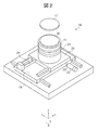
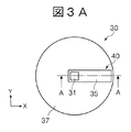
- FIG. 2 is a perspective view showing a schematic structure of a stage and its driving mechanism provided in the prober of FIG. 3A is a diagram showing a schematic configuration of a position inspection unit that can be attached to and detached from the prober of FIG.
- FIG. 3B is a diagram showing a schematic configuration of the position accuracy inspection apparatus according to the embodiment of the present invention.
- FIGS. 4A and 4B are diagrams schematically showing the contents of image processing in the first usage method of the position accuracy inspection apparatus according to the embodiment of the present invention.
- the main body 12 has a hollow casing shape inside.
- the ceiling portion 12 a of the main body 12 is provided with an opening 12 b that opens above the wafer W placed on the stage 11.
- a probe card 17 (see FIG. 2), which will be described later, is disposed in the opening 12b, and the probe card 17 faces the wafer W.
- the wafer W is electrostatically attracted to the stage 11 so that the relative position with respect to the stage 11 does not shift.
- the test head 14 has a rectangular shape and is configured to be rotatable upward by a hinge mechanism 15 provided on the main body 12. When the test head 14 covers the main body 12, the test head 14 is electrically connected to the probe card 17 through a contact ring (not shown).
- the test head 14 also includes a data storage unit (not shown) that stores electrical signals indicating electrical characteristics of the semiconductor device transmitted from the probe card 17 as measurement data, and a semiconductor of the wafer W to be inspected based on the measurement data.
- a determination unit (not shown) that determines the presence or absence of an electrical defect in the device is included.
- a predetermined number of probe needles (not shown) are arranged on the lower surface of the probe card 17 in correspondence with the electrode pads and solder bumps of the semiconductor device formed on the wafer W.
- the stage 11 adjusts the relative positions of the probe card 17 and the wafer W to bring the electrode pads of the semiconductor device into contact with the probe needles.
- FIG. 2 is a perspective view showing a schematic configuration of a moving mechanism of the stage 11 provided in the prober 10.
- the moving mechanism 18 of the stage 11 includes a Y stage 19 that moves along the Y direction shown in FIG. 2, and an X stage 20 that moves along the X direction shown in FIG. And a Z moving part 21 that moves along the Z direction shown in the figure.
- the position accuracy inspection apparatus 100 removes the probe card 17 attached to the prober 10 described with reference to FIGS. 1 and 2, attaches the position inspection unit 30 shown in FIG. 3A instead of the probe card 17,
- the image signal output from the imaging unit 40 provided in the position inspection unit 30 is analyzed by the computer 50.
- the imaging unit 40 is shown in a cross-sectional view taken along the line AA in FIG. 3A.
- the function of the computer 50 can be assigned to a computer that controls the operation of the prober 10.
- the probe card 17 is positioned with extremely high accuracy and is held by the main body 12.
- the position inspection unit 30 is also positioned and held by the main body 12.
- the position inspection unit 30 includes a holding substrate 37 and an imaging unit 40, and the outer diameter of the holding substrate 37 is the same as the outer diameter of the probe card 17.
- the method of holding the imaging unit 40 by the holding substrate 37 is not particularly limited, but a holding method that does not cause the positional shift of the imaging unit 40 with respect to the holding substrate 37 is not used.
- the imaging unit 40 includes a housing 35, a reticle 31, a mirror 32, an imaging element 33, and a lens 34.
- a window portion is formed in a portion corresponding to the center of the holding substrate 37 in the case 35 so as to close the window portion.
- a reticle 31 is attached to the housing 35.
- the reticle 31 is a glass substrate having translucency. As shown in FIG. 4A to be described later, the reticle 31 is formed with a figure (pattern) corresponding to the shape of the electrode pad or solder bump of the semiconductor device to be inspected. The reticle 31 can be exchanged according to the shape of the semiconductor device to be inspected.
- the center of the reticle 31 and the center of the holding substrate 37 coincide with each other with high accuracy when the imaging unit 40 is held on the holding substrate 37.
- the position where the reticle 31 is attached corresponds to the position where the probe needle is arranged in the probe card 17 with high accuracy. That is, when the probe card 17 and the position inspection unit 30 are overlapped in the thickness direction so that the outer circumferences coincide with each other and viewed from the thickness direction, the region where the probe needle is provided and the region of the reticle 31 overlap. .
- the imaging unit 40 performs imaging by observing the wafer W placed on the stage 11 from directly above the stage 11 through the reticle 31.
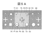
- each of the figures 61 to 64 corresponds to the position of the probe needle.
- the region corresponding to the regions of the figures 61 to 65 is a region that is substantially transparent and transmits light well, and is a region excluding the region 60 from the region 66 (gray) The same applies to the area corresponding to the area indicated by.
- the area corresponding to the area excluding the figures 61 to 65 from the area 60 has a light transmittance smaller than the area of the figures 61 to 65. ing.
- the shapes of the figures 61 to 64 are set to be similar to the shapes of the electrode pads 71 to 74, and the outer shape of the figures 61 to 64 is slightly larger than the outer shape of the electrode pads 71 to 74. Yes.
- the coordinates of the centers of the graphics 61 to 64 and the coordinates of the centers of the electrode pads 71 to 74 are obtained by image processing, regardless of the shapes of the graphics 61 to 64 and the electrode pads 71 to 74. It can be determined separately.
- the shape of the figure 65 is not completely similar to the shape of the electrode pad 75, but the electrode pad 75 is included in the figure 65 when the center coordinates of the figure 65 coincide with the center coordinates of the electrode pad 75. Is set to a size. Further, the figure formed on the reticle 31 is not necessarily similar to the shape of the electrode pad or solder bump, and may be overlapped with the electrode pad or solder bump when imaged by the imaging unit 40 as will be described later. Any shape that can be distinguished from the electrode pads and the solder bumps may be used.
- the electrode pads 71 to 74 and the probe needle may not be in good contact. Therefore, it is determined whether or not the electrode pads 71 to 74 of the semiconductor device are positioned within the allowable region with respect to the probe needle (contact accuracy between the electrode pads and solder bumps formed on the semiconductor device and the probe needle (hereinafter referred to as “the probe needle”).
- the probe needle contact accuracy between the electrode pads and solder bumps formed on the semiconductor device and the probe needle
- the probe needle contact accuracy between the electrode pads and solder bumps formed on the semiconductor device and the probe needle
- a determination criterion is provided for the positional relationship between the figures 61 to 64 and the electrode pads 71 to 74. When this criterion is satisfied, the contact accuracy is determined to be acceptable, and when this criterion is not satisfied, the contact accuracy is determined to be unacceptable.
- the criteria for determining the positional relationship between the figures 61 to 64 and the electrode pads 71 to 74 are not particularly limited. For example, if the electrode pads 71 to 74 are within the respective areas of the figures 61 to 64, contact is made. A criterion for determining the accuracy as acceptable may be used, and according to the criterion, the state of FIG. 4B is determined as acceptable. Further, if the distance between the centers of the electrode pads 71 to 74 and the centers of the figures 61 to 64 is within a predetermined threshold Th, a determination criterion for determining that the contact accuracy is acceptable can be used.
- position control is strictly performed in the manufacturing process of the semiconductor device, so it is not necessary to perform pass / fail determination of the contact accuracy for other semiconductor devices. You may make it perform the pass / fail determination of contact accuracy about several semiconductor devices. As a result of performing the pass / fail judgment of the contact accuracy for a plurality of semiconductor devices, if a semiconductor device that fails the contact accuracy appears, position correction of the stage 11 by the second usage method of the position accuracy inspection apparatus 100 described later I do.
- the position accuracy inspection apparatus 100 it is possible to perform contact accuracy inspection and pass / fail determination at a submicron level with higher accuracy than before. Further, the positional deviation between the figure formed on the reticle 31 and the electrode pad formed on the wafer W can be quantitatively grasped by image processing. Furthermore, since the probe pad needle does not actually mark the electrode pad or the like as in the prior art, it is possible to determine the pass / fail accuracy of the contact accuracy in advance on the wafer W to be inspected without using the reference wafer. .
- the coordinates of P1 and P3 move to P1 ′ (x1 ′, y1 ′) and P3 ′ (x3 ′, y3 ′) by the ⁇ direction correction, respectively.
- the average value of ⁇ X1 and ⁇ X2 as the X direction correction amount ⁇ X An average value of ⁇ Y1 and ⁇ Y2 may be adopted as the Y direction correction amount ⁇ Y.
- the computer 50 stores the obtained X direction correction amount ⁇ X and Y direction correction amount ⁇ Y.
- the computer 50 supplies signals for driving the X-stage motor 25 and the Y-stage motor 23 to the motor control device 27 so that P1 ′ is set to P0 and P3 ′ is set to P2.
- Driving is performed by the direction correction amount ⁇ X and the Y direction correction amount ⁇ Y, and the pass / fail judgment of the contact accuracy by the first usage method described above is performed.
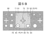
- FIG. 5B shows the positional relationship between the figures 61 to 65 and the electrode pads 71 to 75 after performing the ⁇ direction correction, the X direction correction, and the Y direction correction.
- the coordinates of the stage 11 so that the coordinates of the centers of the figures 61 to 65 coincide with the coordinates of the centers of the electrode pads 71 to 75, and the electrode pads 71 to 75 are positioned at the centers of the figures 61 to 65, respectively. It can be seen that the position of the wafer W) has been corrected. Thus, the contact accuracy is determined to be acceptable.
- the correction parameters ( ⁇ correction amount, X direction correction amount ⁇ X, Y direction correction amount ⁇ Y) obtained by the second usage method of the position accuracy inspection apparatus 100 are used. Using, the position of the wafer W with respect to the probe needle is corrected. Thus, the probe needle can be reliably brought into contact with the electrode pad or solder bump of the semiconductor device formed on the wafer W.
- the centers of the figures 62 and 64 and the centers of the electrode pads 72 and 74 are made coincident with each other at two diagonal positions.
- the present invention is not limited to this, and the other two places are made coincident.
- three or more centers may be matched with a predetermined accuracy.
- the position of the stage 11 is corrected by the second usage method.
- the present invention is not limited to this, and even when the pass / fail judgment of the contact accuracy is passed, when the center of the figure and the center of the electrode pad do not coincide with the predetermined accuracy (accuracy higher than the criterion)
- the position of the stage 11 may be corrected by the second usage method.
- a third method of using the position accuracy inspection apparatus 100 is to sequentially perform the first use of the position accuracy inspection apparatus 100 for a plurality of semiconductor devices formed on the wafer W while scanning the stage 11 in the X direction and the Y direction, respectively. The pass / fail judgment of the contact accuracy described in the method of use is performed.
- the contact accuracy of the semiconductor device at the first measurement point is acceptable, the component accuracy and assembly accuracy of the stage 11, wear of the component due to sliding over time, rattling, and the position where the semiconductor device is formed on the wafer W
- the contact accuracy of the semiconductor device at the measurement point after moving a predetermined distance in the X direction or the Y direction may be rejected due to reasons such as the occurrence of deviation.
- the coordinates of the semiconductor device in which the contact accuracy is determined to be unacceptable are stored, and the position correction of the stage 11 described in the second usage method of the position accuracy inspection apparatus 100 is performed on the semiconductor device. Thereafter, the pass / fail judgment of the contact accuracy described in the first usage method of the position accuracy inspection apparatus 100 is continued for the remaining semiconductor devices in the X direction and the Y direction.
- the drive characteristic data of the stage 11 obtained in this way is used for driving the stage 11 when the prober 10 inspects the electrical characteristics. Accordingly, the probe needle can be reliably brought into contact with the electrode pad of the semiconductor device formed on the wafer W. Further, it can be inspected whether or not the stage 11 is accurately driven in the X direction and the Y direction.
- the pass / fail judgment of contact accuracy is performed for all semiconductor devices formed on the wafer W by the third method of use, and the drive profile of the stage 11 that passes the contact accuracy for all semiconductor devices (the position correction of the stage 11 is performed).
- the electrical characteristics of the prober 10 may be inspected using the stored drive profile of the stage 11.
- the pass / fail judgment of the contact accuracy according to the first usage method of the positional accuracy inspection apparatus 100 is performed on two or more semiconductor devices without moving the stage 11 (wafer W). Against.
- FIG. 6 is a back view showing a schematic configuration of a position inspection unit 30A used for executing the fourth usage method of the position accuracy inspection apparatus 100.
- the position inspection unit 30A includes two imaging units 40 and 40A having the same structure.
- the positions at which the reticles 31 of the imaging units 40 and 40A are arranged are aligned with the positions of the semiconductor devices formed on the wafer W to be inspected.
- the determination accuracy can be improved by performing the pass / fail determination of the contact accuracy for the two semiconductor devices. Note that when the contact accuracy of at least one semiconductor device fails, the position of the stage 11 is corrected by the second usage method of the position accuracy inspection apparatus 100.
- the reticle 31 is arranged at the center and the outer edge of the holding substrate 37.
- the arrangement position of the reticle 31, that is, the observation position of the semiconductor device formed on the wafer W is limited to this.
- the imaging units 40 and 40A may be held by the holding substrate 37 so that the reticles 31 (observation positions) are arranged at two arbitrary positions. Further, a configuration in which three or more imaging units are arranged on the holding substrate 37 may be adopted.
- the coordinate accuracy of the stage 11 and the alignment accuracy of the wafer W with respect to the stage 11 can be inspected without leaving a needle mark on the reference wafer.
- the reference wafer is a wafer in which a semiconductor device equivalent to the wafer W to be inspected for electrical characteristics by the prober 10 (see FIGS. 1 and 2) is formed, and the position (coordinates) of the formed semiconductor device is known. is there.
Landscapes
- Physics & Mathematics (AREA)
- General Physics & Mathematics (AREA)
- Engineering & Computer Science (AREA)
- General Engineering & Computer Science (AREA)
- Computer Hardware Design (AREA)
- Microelectronics & Electronic Packaging (AREA)
- Testing Or Measuring Of Semiconductors Or The Like (AREA)
- Length Measuring Devices By Optical Means (AREA)
- Tests Of Electronic Circuits (AREA)
Abstract
Description
[図2]図1のプローバが備えるステージとその駆動機構の概略構造を示す斜視図である。
[図3A]図1のプローバに着脱可能な位置検査ユニットの概略構成を示す図である。
[図3B]本発明の実施の形態に係る位置精度検査装置の概略構成を示す図である。
[図4A及び図4B]本発明の実施の形態に係る位置精度検査装置の第1の使用方法での画像処理の内容を模式的に示す図である。
[図5A及び図5B]本発明の実施の形態に係る位置精度検査装置の第2の使用方法での画像処理の内容を模式的に示す図である。
[図6]本発明の実施の形態に係る位置精度検査装置の第4の使用方法を実行するために用いられる位置検査ユニットの概略構成を示す裏面図である。
31 レチクル
33 撮像素子
40,40A 撮像ユニット
61,62,63,64.65 図形
71,72,73,74,75 電極パッド
100 位置精度検査装置
Claims (12)
- 被検査基板に形成された被検査チップの特定の領域に対して探針による接触式検査を行う際の接触位置を検査する位置精度検査方法であって、
前記被検査基板を基板載置台に載置する載置ステップと、
前記探針が配置される位置に、前記探針に代えて、前記被検査基板に接触させる前記探針の位置を示す図形が形成されたガラス基板を配置し、前記ガラス基板を通して前記被検査基板に形成された前記被検査チップを撮像する撮像ステップと、
前記撮像ステップにより得られた画像から、前記図形と前記特定の領域との位置関係を解析する解析ステップと、を有することを特徴とする位置精度検査方法。 - 前記解析ステップにより得られた前記図形と前記特定の領域との位置関係に基づいて、前記探針を前記特定の領域に接触させることができるか否かを判定する判定ステップを有することを特徴とする請求項1記載の位置精度検査方法。
- 前記判定ステップでは、前記図形の中心と前記特定の領域の中心との距離が予め定められた所定の閾値以内であるときに、前記探針を前記特定の領域に接触させることができると判定することを特徴とする請求項2記載の位置精度検査方法。
- 前記判定ステップにおいて前記図形の中心と前記特定の領域の中心とが所定の精度で一致しないと判定されたときに、前記図形の中心と前記特定の領域の中心とが一致するように前記基板載置台の座標を補正する補正ステップを有することを特徴とする請求項2又は3記載の位置精度検査方法。
- 前記撮像ステップにおいて、前記基板載置台を動かさずに前記ガラス基板を通して前記被検査基板に形成された前記被検査チップを少なくとも2つ以上撮像し、
得られた各画像に対して前記解析ステップと前記判定ステップを行い、少なくとも1つの画像について前記図形の中心と前記特定の領域の中心とが所定の精度で一致しないと判定されたときに前記補正ステップを実行することを特徴とする請求項4に記載の位置精度検査方法。 - 前記被検査基板は、半導体ウエハであり、
前記被検査チップは、半導体デバイスであり、
前記特定の領域は、前記半導体デバイスの電極パッド又は半田バンプであることを特徴とする請求項1乃至5のいずれか1項に記載の位置精度検査方法。 - 被検査基板に形成された被検査チップの特定の領域に対して探針による接触式検査を行う際の接触位置を検査する位置精度検査装置であって、
前記被検査基板を載置する基板載置台と、
前記基板載置台の上方に配置される撮像ユニットと、
前記撮像ユニットにより撮像された画像を解析する解析装置とを備え、
前記撮像ユニットは、
前記探針が配置される位置に前記探針に代えて配置され、前記被検査基板に接触させる前記探針の位置を示す図形が形成されたガラス基板と、
前記ガラス基板を通して前記基板載置台に載置された前記被検査基板を撮像する撮像素子とを有し、
前記解析装置は、前記ガラス基板を通して前記被検査基板に形成された前記被検査チップを撮像して得られた画像から、前記図形と前記特定の領域との位置関係を解析することを特徴とする位置精度検査装置。 - 複数の前記撮像ユニットを備えることを特徴とする請求項7記載の位置精度検査装置。
- 前記解析装置は、前記図形と前記特定の領域との位置関係に基づいて、前記探針を前記特定の領域に接触させることができるか否かを判定することを特徴とする請求項7又は8記載の位置精度検査装置。
- 前記基板載置台の載置面と平行な面内方向で前記基板載置台を移動させると共に、前記載置面と直交する軸を中心として前記基板載置台を回転させる駆動装置を備え、
前記解析装置は、前記図形の中心と前記特定の領域の中心とが所定の精度で一致しないと判定したときに、前記図形の中心と前記特定の領域の中心とが一致するように前記駆動装置を制御して前記基板載置台の座標を補正することを特徴とする請求項9記載の位置精度検査装置。 - 前記被検査基板は、半導体ウエハであり、
前記被検査チップは、半導体デバイスであり、
前記特定の領域は、前記半導体デバイスの電極パッド又は半田バンプであることを特徴とする請求項7乃至10のいずれか1項に記載の位置精度検査装置。 - 半導体ウエハに形成された半導体デバイスの電極パッド又は半田バンプに対してプローブ針を接触させて電気的特性を検査する際に、前記電極パッド又は前記半田バンプに対する前記プローブ針の接触位置を事前に検査するために前記半導体ウエハの上方に配置される位置検査ユニットであって、
前記位置検査ユニットは、
撮像ユニットと、
前記撮像ユニットを保持する保持基板とを備え、
前記撮像ユニットは、
前記プローブ針が配置される位置に前記プローブ針に代えて配置され、前記プローブ針の位置を示す図形が形成されたガラス基板と、
前記ガラス基板を通して前記半導体ウエハに形成された前記半導体デバイスを撮像する撮像素子とを有することを特徴とする位置検査ユニット。
Priority Applications (4)
| Application Number | Priority Date | Filing Date | Title |
|---|---|---|---|
| CN201580052496.XA CN107078072B (zh) | 2014-09-30 | 2015-08-19 | 位置精度检查方法、位置精度检查装置以及位置检查单元 |
| KR1020177008504A KR101865887B1 (ko) | 2014-09-30 | 2015-08-19 | 위치 정밀도 검사 방법, 위치 정밀도 검사 장치 및 위치 검사 유닛 |
| SG11201702570TA SG11201702570TA (en) | 2014-09-30 | 2015-08-19 | Position accuracy inspecting method, position accuracy inspecting apparatus, and position inspecting unit |
| US15/515,241 US10006941B2 (en) | 2014-09-30 | 2015-08-19 | Position accuracy inspecting method, position accuracy inspecting apparatus, and position inspecting unit |
Applications Claiming Priority (2)
| Application Number | Priority Date | Filing Date | Title |
|---|---|---|---|
| JP2014-200912 | 2014-09-30 | ||
| JP2014200912A JP6462296B2 (ja) | 2014-09-30 | 2014-09-30 | 位置精度検査方法、位置精度検査装置及び位置検査ユニット |
Publications (1)
| Publication Number | Publication Date |
|---|---|
| WO2016052012A1 true WO2016052012A1 (ja) | 2016-04-07 |
Family
ID=55630058
Family Applications (1)
| Application Number | Title | Priority Date | Filing Date |
|---|---|---|---|
| PCT/JP2015/073923 Ceased WO2016052012A1 (ja) | 2014-09-30 | 2015-08-19 | 位置精度検査方法、位置精度検査装置及び位置検査ユニット |
Country Status (7)
| Country | Link |
|---|---|
| US (1) | US10006941B2 (ja) |
| JP (1) | JP6462296B2 (ja) |
| KR (1) | KR101865887B1 (ja) |
| CN (1) | CN107078072B (ja) |
| SG (1) | SG11201702570TA (ja) |
| TW (1) | TWI697970B (ja) |
| WO (1) | WO2016052012A1 (ja) |
Cited By (1)
| Publication number | Priority date | Publication date | Assignee | Title |
|---|---|---|---|---|
| CN107507783A (zh) * | 2016-06-14 | 2017-12-22 | 豪威科技股份有限公司 | 用于重组晶圆的测试系统及其方法 |
Families Citing this family (25)
| Publication number | Priority date | Publication date | Assignee | Title |
|---|---|---|---|---|
| CN108627096A (zh) * | 2017-05-10 | 2018-10-09 | 新疆畜牧科学院畜牧业质量标准研究所 | 毛绒细度长度测量专用毛绒样品成像扫描仪 |
| JP6999321B2 (ja) * | 2017-07-31 | 2022-01-18 | 東京エレクトロン株式会社 | 検査装置、検査方法及び記憶媒体 |
| TWI652483B (zh) * | 2017-12-12 | 2019-03-01 | 穩懋半導體股份有限公司 | 用於晶圓針測系統之非均質性接收器與非等向性發射器之對位方法 |
| JP7018784B2 (ja) * | 2018-02-23 | 2022-02-14 | 東京エレクトロン株式会社 | コンタクト精度保証方法および検査装置 |
| TWI694537B (zh) * | 2018-07-08 | 2020-05-21 | 香港商康代影像技術方案香港有限公司 | 用於失準補償之系統及方法 |
| CN109239422B (zh) * | 2018-10-24 | 2023-11-21 | 安徽爱意爱机电科技有限公司 | 厚膜混合电路烧结后电阻阻值调节过程中使用的探针卡 |
| KR102111095B1 (ko) * | 2018-11-09 | 2020-05-15 | (주)에이앤아이 | 전력전달유닛을 포함하는 무선 로터리 검사장치 |
| CN111223786B (zh) * | 2018-11-27 | 2023-10-27 | 东京毅力科创株式会社 | 检查装置系统 |
| JP2020092140A (ja) * | 2018-12-04 | 2020-06-11 | 東京エレクトロン株式会社 | 位置測定装置、及び、位置測定方法 |
| JP7220554B2 (ja) * | 2018-12-04 | 2023-02-10 | 東京エレクトロン株式会社 | プローブ装置、及び、プローブ装置の調整方法 |
| JP7108527B2 (ja) * | 2018-12-10 | 2022-07-28 | 東京エレクトロン株式会社 | 解析装置及び画像生成方法 |
| KR20200106774A (ko) | 2019-03-05 | 2020-09-15 | 세메스 주식회사 | 반도체 소자 검사 방법 및 장치 |
| KR102696994B1 (ko) | 2019-03-06 | 2024-08-19 | 세메스 주식회사 | 척 구조물 및 이를 포함하는 프로브 스테이션 |
| JP7218909B2 (ja) * | 2019-05-09 | 2023-02-07 | 株式会社昭和真空 | プローブピン位置合せ装置及びプローブピン位置合せ装置を使用した電子デバイスの製造方法 |
| KR102199108B1 (ko) * | 2019-12-03 | 2021-01-06 | 티아이에스 주식회사 | 웨이퍼 검사장치 |
| JP7382888B2 (ja) * | 2020-04-06 | 2023-11-17 | 東京エレクトロン株式会社 | 検査装置、及び、検査装置の制御方法 |
| TWI759902B (zh) * | 2020-10-13 | 2022-04-01 | 豪勉科技股份有限公司 | 點測裝置 |
| JP7638723B2 (ja) * | 2021-02-18 | 2025-03-04 | 東京エレクトロン株式会社 | 検査装置のセットアップ方法及び検査装置 |
| JP7727169B2 (ja) * | 2021-06-04 | 2025-08-21 | 株式会社東京精密 | プローバ制御装置、プローバ制御方法、及びプローバ |
| JP7737852B2 (ja) * | 2021-09-28 | 2025-09-11 | 東京エレクトロン株式会社 | 検査装置及び検査方法 |
| CN113985246B (zh) * | 2021-10-21 | 2024-09-03 | 武汉光谷信息光电子创新中心有限公司 | 一种芯片的测试与封装工装及系统 |
| CN114325351A (zh) * | 2022-03-15 | 2022-04-12 | 武汉普赛斯电子技术有限公司 | 激光器芯片测试装置和激光器芯片测试方法 |
| US12237198B2 (en) | 2022-03-31 | 2025-02-25 | Onto Innovation Inc. | Area camera substrate pre-aligner |
| TWI868854B (zh) * | 2022-09-23 | 2025-01-01 | 旺矽科技股份有限公司 | 探針卡裝置、探針系統及待測物的檢測方法 |
| CN115951103B (zh) * | 2023-01-03 | 2026-04-21 | 矽电半导体设备(深圳)股份有限公司 | 晶圆测试装置及晶圆测试方法 |
Citations (2)
| Publication number | Priority date | Publication date | Assignee | Title |
|---|---|---|---|---|
| JP2001156127A (ja) * | 1999-11-29 | 2001-06-08 | Yokogawa Electric Corp | 半導体製造装置 |
| JP2001264392A (ja) * | 2000-03-21 | 2001-09-26 | Mitsubishi Materials Corp | コンタクトプローブの位置調整装置 |
Family Cites Families (10)
| Publication number | Priority date | Publication date | Assignee | Title |
|---|---|---|---|---|
| JPS63305525A (ja) * | 1987-06-05 | 1988-12-13 | Tokyo Kasoode Kenkyusho:Kk | 半導体ウエハ検査におけるプロ−ブヘツドの位置合わせ方法 |
| US5416592A (en) | 1992-03-23 | 1995-05-16 | Tokyo Electron Kabushiki Kaisha | Probe apparatus for measuring electrical characteristics of objects |
| JP3156192B2 (ja) | 1994-04-19 | 2001-04-16 | 東京エレクトロン株式会社 | プローブ方法及びその装置 |
| US6549649B1 (en) * | 1999-03-04 | 2003-04-15 | Electroglas, Inc. | Apparatus and method for projecting an alignment image |
| US6710798B1 (en) * | 1999-03-09 | 2004-03-23 | Applied Precision Llc | Methods and apparatus for determining the relative positions of probe tips on a printed circuit board probe card |
| US8466703B2 (en) * | 2003-03-14 | 2013-06-18 | Rudolph Technologies, Inc. | Probe card analysis system and method |
| JP4908138B2 (ja) * | 2005-12-09 | 2012-04-04 | ルネサスエレクトロニクス株式会社 | プローブ検査装置 |
| JP4996119B2 (ja) * | 2006-03-30 | 2012-08-08 | 東京エレクトロン株式会社 | プローブの先端位置の検出方法、この方法を記録した記憶媒体、及びプローブ装置 |
| US8159243B2 (en) * | 2008-11-13 | 2012-04-17 | Dcg Systems, Inc. | Probe tip to device pad alignment in obscured view probing applications |
| JP2010182874A (ja) * | 2009-02-05 | 2010-08-19 | Oki Semiconductor Co Ltd | プローブカードのメンテナンス方法 |
-
2014
- 2014-09-30 JP JP2014200912A patent/JP6462296B2/ja active Active
-
2015
- 2015-08-19 CN CN201580052496.XA patent/CN107078072B/zh active Active
- 2015-08-19 US US15/515,241 patent/US10006941B2/en active Active
- 2015-08-19 WO PCT/JP2015/073923 patent/WO2016052012A1/ja not_active Ceased
- 2015-08-19 KR KR1020177008504A patent/KR101865887B1/ko active Active
- 2015-08-19 SG SG11201702570TA patent/SG11201702570TA/en unknown
- 2015-09-22 TW TW104131264A patent/TWI697970B/zh active
Patent Citations (2)
| Publication number | Priority date | Publication date | Assignee | Title |
|---|---|---|---|---|
| JP2001156127A (ja) * | 1999-11-29 | 2001-06-08 | Yokogawa Electric Corp | 半導体製造装置 |
| JP2001264392A (ja) * | 2000-03-21 | 2001-09-26 | Mitsubishi Materials Corp | コンタクトプローブの位置調整装置 |
Cited By (2)
| Publication number | Priority date | Publication date | Assignee | Title |
|---|---|---|---|---|
| CN107507783A (zh) * | 2016-06-14 | 2017-12-22 | 豪威科技股份有限公司 | 用于重组晶圆的测试系统及其方法 |
| CN107507783B (zh) * | 2016-06-14 | 2020-10-13 | 豪威科技股份有限公司 | 用于重组晶圆的测试系统及其方法 |
Also Published As
| Publication number | Publication date |
|---|---|
| TW201631678A (zh) | 2016-09-01 |
| JP6462296B2 (ja) | 2019-01-30 |
| US10006941B2 (en) | 2018-06-26 |
| US20170219625A1 (en) | 2017-08-03 |
| TWI697970B (zh) | 2020-07-01 |
| KR101865887B1 (ko) | 2018-06-08 |
| CN107078072B (zh) | 2019-02-05 |
| SG11201702570TA (en) | 2017-04-27 |
| KR20170061135A (ko) | 2017-06-02 |
| JP2016072455A (ja) | 2016-05-09 |
| CN107078072A (zh) | 2017-08-18 |
Similar Documents
| Publication | Publication Date | Title |
|---|---|---|
| JP6462296B2 (ja) | 位置精度検査方法、位置精度検査装置及び位置検査ユニット | |
| KR100786463B1 (ko) | 두 물체의 위치 정렬 방법, 두 물체의 중첩 상태의 검출방법 및 두 물체의 위치 정렬 장치 | |
| US6549825B2 (en) | Alignment apparatus | |
| JP5193112B2 (ja) | 半導体ウエーハ外観検査装置の検査条件データ生成方法及び検査システム | |
| JP6903270B2 (ja) | 電子部品搬送装置および電子部品検査装置 | |
| TWI484164B (zh) | Optical re - inspection system and its detection method | |
| JP2010522441A (ja) | 半導体ウエハの異物検査及びリペアシステムとその方法 | |
| JPWO2009031612A1 (ja) | 観察装置および観察方法、並びに検査装置および検査方法 | |
| JPWO2007141857A1 (ja) | 外観検査装置 | |
| JP2018195735A (ja) | 半導体製造装置および半導体装置の製造方法 | |
| KR102219110B1 (ko) | 검사 장치, 검사 방법 및 기억 매체 | |
| JP5273926B2 (ja) | 欠陥検査装置 | |
| WO2015174114A1 (ja) | 基板検査装置 | |
| JPWO2009072483A1 (ja) | 観察装置および観察方法 | |
| JP6746744B1 (ja) | 検査装置及び検査方法 | |
| JP5272784B2 (ja) | 光学的検査方法および光学的検査装置 | |
| JP2009052966A (ja) | 基板検査装置 | |
| JP2007234932A (ja) | 外観検査装置 | |
| JP5316924B2 (ja) | 観察装置および観察方法 | |
| JP5455957B2 (ja) | 半導体素子の故障解析方法及び故障解析装置 | |
| JP4981703B2 (ja) | 外観検査装置および外観検査方法 | |
| JP2008261692A (ja) | 基板検査システム及び基板検査方法 | |
| US20100150430A1 (en) | Visual inspection apparatus and visual inspection method for semiconductor laser chip or semiconductor laser bar | |
| JP2009198395A (ja) | 表面検査装置 | |
| JP5319063B2 (ja) | 線幅測定装置 |
Legal Events
| Date | Code | Title | Description |
|---|---|---|---|
| 121 | Ep: the epo has been informed by wipo that ep was designated in this application |
Ref document number: 15848006 Country of ref document: EP Kind code of ref document: A1 |
|
| ENP | Entry into the national phase |
Ref document number: 20177008504 Country of ref document: KR Kind code of ref document: A |
|
| WWE | Wipo information: entry into national phase |
Ref document number: 15515241 Country of ref document: US |
|
| NENP | Non-entry into the national phase |
Ref country code: DE |
|
| 122 | Ep: pct application non-entry in european phase |
Ref document number: 15848006 Country of ref document: EP Kind code of ref document: A1 |