WO2016047216A1 - 光電変換素子 - Google Patents
光電変換素子 Download PDFInfo
- Publication number
- WO2016047216A1 WO2016047216A1 PCT/JP2015/066641 JP2015066641W WO2016047216A1 WO 2016047216 A1 WO2016047216 A1 WO 2016047216A1 JP 2015066641 W JP2015066641 W JP 2015066641W WO 2016047216 A1 WO2016047216 A1 WO 2016047216A1
- Authority
- WO
- WIPO (PCT)
- Prior art keywords
- electrode
- photoelectric conversion
- conversion element
- buffer layer
- element according
- Prior art date
- Legal status (The legal status is an assumption and is not a legal conclusion. Google has not performed a legal analysis and makes no representation as to the accuracy of the status listed.)
- Ceased
Links
Images


Classifications
-
- H—ELECTRICITY
- H10—SEMICONDUCTOR DEVICES; ELECTRIC SOLID-STATE DEVICES NOT OTHERWISE PROVIDED FOR
- H10K—ORGANIC ELECTRIC SOLID-STATE DEVICES
- H10K30/00—Organic devices sensitive to infrared radiation, light, electromagnetic radiation of shorter wavelength or corpuscular radiation
- H10K30/30—Organic devices sensitive to infrared radiation, light, electromagnetic radiation of shorter wavelength or corpuscular radiation comprising bulk heterojunctions, e.g. interpenetrating networks of donor and acceptor material domains
- H10K30/353—Organic devices sensitive to infrared radiation, light, electromagnetic radiation of shorter wavelength or corpuscular radiation comprising bulk heterojunctions, e.g. interpenetrating networks of donor and acceptor material domains comprising blocking layers, e.g. exciton blocking layers
-
- H—ELECTRICITY
- H01—ELECTRIC ELEMENTS
- H01G—CAPACITORS; CAPACITORS, RECTIFIERS, DETECTORS, SWITCHING DEVICES, LIGHT-SENSITIVE OR TEMPERATURE-SENSITIVE DEVICES OF THE ELECTROLYTIC TYPE
- H01G9/00—Electrolytic capacitors, rectifiers, detectors, switching devices, light-sensitive or temperature-sensitive devices; Processes of their manufacture
- H01G9/20—Light-sensitive devices
- H01G9/2004—Light-sensitive devices characterised by the electrolyte, e.g. comprising an organic electrolyte
- H01G9/2018—Light-sensitive devices characterised by the electrolyte, e.g. comprising an organic electrolyte characterised by the ionic charge transport species, e.g. redox shuttles
-
- H—ELECTRICITY
- H10—SEMICONDUCTOR DEVICES; ELECTRIC SOLID-STATE DEVICES NOT OTHERWISE PROVIDED FOR
- H10K—ORGANIC ELECTRIC SOLID-STATE DEVICES
- H10K30/00—Organic devices sensitive to infrared radiation, light, electromagnetic radiation of shorter wavelength or corpuscular radiation
- H10K30/30—Organic devices sensitive to infrared radiation, light, electromagnetic radiation of shorter wavelength or corpuscular radiation comprising bulk heterojunctions, e.g. interpenetrating networks of donor and acceptor material domains
-
- H—ELECTRICITY
- H10—SEMICONDUCTOR DEVICES; ELECTRIC SOLID-STATE DEVICES NOT OTHERWISE PROVIDED FOR
- H10K—ORGANIC ELECTRIC SOLID-STATE DEVICES
- H10K30/00—Organic devices sensitive to infrared radiation, light, electromagnetic radiation of shorter wavelength or corpuscular radiation
- H10K30/80—Constructional details
- H10K30/81—Electrodes
- H10K30/82—Transparent electrodes, e.g. indium tin oxide [ITO] electrodes
-
- H—ELECTRICITY
- H10—SEMICONDUCTOR DEVICES; ELECTRIC SOLID-STATE DEVICES NOT OTHERWISE PROVIDED FOR
- H10K—ORGANIC ELECTRIC SOLID-STATE DEVICES
- H10K30/00—Organic devices sensitive to infrared radiation, light, electromagnetic radiation of shorter wavelength or corpuscular radiation
- H10K30/50—Photovoltaic [PV] devices
-
- H—ELECTRICITY
- H10—SEMICONDUCTOR DEVICES; ELECTRIC SOLID-STATE DEVICES NOT OTHERWISE PROVIDED FOR
- H10K—ORGANIC ELECTRIC SOLID-STATE DEVICES
- H10K85/00—Organic materials used in the body or electrodes of devices covered by this subclass
- H10K85/10—Organic polymers or oligomers
- H10K85/111—Organic polymers or oligomers comprising aromatic, heteroaromatic, or aryl chains, e.g. polyaniline, polyphenylene or polyphenylene vinylene
- H10K85/113—Heteroaromatic compounds comprising sulfur or selene, e.g. polythiophene
- H10K85/1135—Polyethylene dioxythiophene [PEDOT]; Derivatives thereof
-
- H—ELECTRICITY
- H10—SEMICONDUCTOR DEVICES; ELECTRIC SOLID-STATE DEVICES NOT OTHERWISE PROVIDED FOR
- H10K—ORGANIC ELECTRIC SOLID-STATE DEVICES
- H10K85/00—Organic materials used in the body or electrodes of devices covered by this subclass
- H10K85/10—Organic polymers or oligomers
- H10K85/151—Copolymers
-
- H—ELECTRICITY
- H10—SEMICONDUCTOR DEVICES; ELECTRIC SOLID-STATE DEVICES NOT OTHERWISE PROVIDED FOR
- H10K—ORGANIC ELECTRIC SOLID-STATE DEVICES
- H10K85/00—Organic materials used in the body or electrodes of devices covered by this subclass
- H10K85/20—Carbon compounds, e.g. carbon nanotubes or fullerenes
- H10K85/211—Fullerenes, e.g. C60
- H10K85/215—Fullerenes, e.g. C60 comprising substituents, e.g. PCBM
-
- Y—GENERAL TAGGING OF NEW TECHNOLOGICAL DEVELOPMENTS; GENERAL TAGGING OF CROSS-SECTIONAL TECHNOLOGIES SPANNING OVER SEVERAL SECTIONS OF THE IPC; TECHNICAL SUBJECTS COVERED BY FORMER USPC CROSS-REFERENCE ART COLLECTIONS [XRACs] AND DIGESTS
- Y02—TECHNOLOGIES OR APPLICATIONS FOR MITIGATION OR ADAPTATION AGAINST CLIMATE CHANGE
- Y02E—REDUCTION OF GREENHOUSE GAS [GHG] EMISSIONS, RELATED TO ENERGY GENERATION, TRANSMISSION OR DISTRIBUTION
- Y02E10/00—Energy generation through renewable energy sources
- Y02E10/50—Photovoltaic [PV] energy
- Y02E10/542—Dye sensitized solar cells
-
- Y—GENERAL TAGGING OF NEW TECHNOLOGICAL DEVELOPMENTS; GENERAL TAGGING OF CROSS-SECTIONAL TECHNOLOGIES SPANNING OVER SEVERAL SECTIONS OF THE IPC; TECHNICAL SUBJECTS COVERED BY FORMER USPC CROSS-REFERENCE ART COLLECTIONS [XRACs] AND DIGESTS
- Y02—TECHNOLOGIES OR APPLICATIONS FOR MITIGATION OR ADAPTATION AGAINST CLIMATE CHANGE
- Y02E—REDUCTION OF GREENHOUSE GAS [GHG] EMISSIONS, RELATED TO ENERGY GENERATION, TRANSMISSION OR DISTRIBUTION
- Y02E10/00—Energy generation through renewable energy sources
- Y02E10/50—Photovoltaic [PV] energy
- Y02E10/549—Organic PV cells
Definitions
- Embodiments of the present invention relate to a photoelectric conversion element.
- Embodiment of this invention provides the photoelectric conversion element which can suppress the fall of shunt resistance.
- the photoelectric conversion element including the first electrode, the second electrode, the photoelectric conversion layer, the first buffer layer, the second buffer layer, and the third buffer layer.
- the second electrode is provided apart from the first electrode.
- the photoelectric conversion layer is provided between the first electrode and the second electrode.
- the first buffer layer is provided between the first electrode and the photoelectric conversion layer.
- the second buffer layer is provided between the second electrode and the photoelectric conversion layer.
- the third buffer layer is provided at an end of the first electrode.
- FIG. 1A to FIG. 1D are schematic views showing a photoelectric conversion element according to an embodiment.
- 2A and 2B are a table and a graph illustrating a first example of the photoelectric conversion element according to the embodiment.
- FIG. 3 shows an EMS image of the photoelectric conversion element according to the first comparative example.
- FIGS. 4A to 4C are schematic views showing a photoelectric conversion element according to the first comparative example.
- FIG. 5 is a graph illustrating a second example of the photoelectric conversion element according to the embodiment.
- FIG. 6A and FIG. 6B are a table and a graph illustrating a third example of the photoelectric conversion element according to the embodiment.
- FIG. 7A and FIG. 7B are a table and a graph illustrating a third example of the photoelectric conversion element according to the embodiment.
- FIG. 1 is a schematic diagram illustrating a photoelectric conversion element according to an embodiment.
- FIG. 1A is a schematic plan view illustrating a photoelectric conversion element according to an embodiment.
- FIG. 1B is a schematic cross-sectional view taken along the section AA shown in FIG.
- FIG. 1C is a schematic cross-sectional view taken along the line BB shown in FIG.
- FIG.1 (d) is the typical enlarged view to which area
- the photoelectric conversion element 10 includes a first electrode 1, a first buffer layer 2, a photoelectric conversion layer 3, a second buffer layer 4, a second electrode 5, a substrate 6, A third buffer layer 7.
- Examples of the photoelectric conversion element 10 according to the embodiment include a solar cell and a sensor.
- the photoelectric conversion layer 3 is formed by coating and includes at least one of an organic semiconductor material and a perovskite structure material.
- the second electrode 5 is provided separately from the first electrode 1.
- the first electrode 1 is provided between the substrate 6 and the second electrode 5.
- the first buffer layer 2 is provided between the first electrode 1 and the second electrode 5.
- the photoelectric conversion layer 3 is provided between the first buffer layer 2 and the second electrode 5.
- the second buffer layer 4 is provided between the photoelectric conversion layer 3 and the second electrode 5.
- the third buffer layer 7 is provided at the end 1 a of the first electrode 1. More specifically, as shown in FIG. 1D, the second electrode 5 includes a first portion 5a and a second portion 5b. The first portion 5 a is provided on the second buffer layer 4. The second portion 5 b extends from the first portion 5 a to the first electrode 1.
- the third buffer layer has a first buffer portion 7a and a second buffer portion 7b.
- the first electrode 1, the first buffer layer 2, the photoelectric conversion layer 3, and the second buffer layer 4 are provided between the substrate 6 and the first portion 5 a of the second electrode 5.
- the first buffer portion 7 a of the third buffer layer 7 is provided between the first electrode 1 and the first portion 5 a of the second electrode 5.
- the second buffer portion 7 b of the third buffer layer 7 is provided between the first electrode 1 and the second portion 5 b of the second electrode 5.
- One of the first electrode 1 and the second electrode 5 serves as an anode.
- One of the first electrode 1 and the second electrode 5 serves as a cathode. Electricity is taken out by the first electrode 1 and the second electrode 5.
- the photoelectric conversion layer 3 is excited by light incident through the substrate 6, the first electrode 1 and the first buffer layer 2, or light incident through the second electrode 5 and the second buffer layer 4. Electrons are generated in one of the first electrode 1 and the second electrode 5, and holes are generated in the other of the first electrode 1 and the second electrode 5.
- the substrate 6 supports other components (components other than the substrate 6).
- the substrate 6 can form an electrode.
- the substrate 6 is preferably one that is not altered by heat or an organic solvent.
- the material of the substrate 6 include inorganic materials, plastics, polymer films, and metal substrates.
- the inorganic material include alkali-free glass and quartz glass.
- the plastic and polymer film materials include polyethylene, polyethylene terephthalate (PET), polyethylene naphthalate (PEN), polyimide, polyamide, polyamideimide, liquid crystal polymer, cycloolefin polymer, and the like.
- the material for the metal substrate include stainless steel (SUS) and silicon.
- a transparent one is used. That is, when the substrate 6 is disposed on the light incident side, a material having optical transparency is used as the material of the substrate 6.
- the electrode opposite to the substrate 6 is transparent or translucent, an opaque substrate may be used as the substrate 6. If the board
- a moth-eye structure antireflection film is provided on the light incident surface, so that the light can be efficiently captured and the energy conversion efficiency of the cell can be improved.
- the moth-eye structure has a regular protrusion arrangement on the surface of the order of 100 nanometers (nm).
- the refractive index in the thickness direction changes continuously due to the projection structure of the moth-eye structure. Therefore, the discontinuous change surface of the refractive index can be reduced by interposing the non-reflective film. This reduces light reflection and improves cell efficiency.
- First electrode 1 and second electrode 5 In the description of the first electrode 1 and the second electrode 5, when the term “electrode” is simply used, it means at least one of the first electrode 1 and the second electrode 5.
- the first electrode 1 and the second electrode 5 are not particularly limited as long as they have conductivity.
- a transparent or translucent conductive material is used as the material of the electrode on the light transmitting side (for example, the first electrode 1).
- the first electrode 1 and the second electrode 5 are formed by vacuum deposition, sputtering, ion plating, plating, coating, or the like.
- the material of the transparent or translucent electrode include conductive metal oxides and translucent metals.
- conductive glass, gold, platinum, silver, copper, or the like is used as the material for the transparent or translucent electrode.
- the material for the conductive glass examples include indium oxide, zinc oxide, tin oxide, and indium tin oxide (ITO), fluorine-doped tin oxide (FTO), indium zinc oxide and the like that are composites thereof.
- the electrode is manufactured as a film (NESA or the like) or a layer containing conductive glass.
- ITO or FTO is preferable as the electrode material.
- the electrode material may be an organic conductive polymer such as polyaniline and derivatives thereof, polythiophene and derivatives thereof, and the like.
- the thickness of the electrode is preferably 30 nm or more and 300 nm or less. If the thickness of the electrode is less than 30 nm, the conductivity is lowered and the resistance is increased. The decrease in conductivity is one of the causes of a decrease in photoelectric conversion efficiency. When the thickness of the electrode is thicker than 300 nm, the flexibility of ITO is lowered. When the flexibility of ITO decreases, the ITO may crack when stress is applied.
- the sheet resistance of the electrode is preferably as low as possible, and is preferably 10 ⁇ / ⁇ or less.
- the electrode may be a single layer or may have a structure in which layers containing materials having different work functions are stacked.
- the electrode When the electrode is formed in contact with the electron transport layer, it is preferable to use a material having a low work function as the electrode material.
- the material having a low work function include alkali metals and alkaline earth metals.
- examples of the material having a low work function include Li, In, Al, Ca, Mg, Sm, Tb, Yb, Zr, Na, K, Rb, Cs, Ba, and alloys thereof.
- the electrode may be a single layer or may have a structure in which layers containing materials having different work functions are stacked.
- the electrode material is an alloy of at least one of the above-described low work function materials and at least one of gold, silver, platinum, copper, manganese, titanium, cobalt, nickel, tungsten, and tin. But you can.
- the alloy include a lithium-aluminum alloy, a lithium-magnesium alloy, a lithium-indium alloy, a magnesium-silver alloy, a calcium-indium alloy, a magnesium-aluminum alloy, an indium-silver alloy, and a calcium-aluminum alloy.
- the thickness of the electrode is preferably 1 nm or more and 500 nm or less.
- the thickness of the electrode is more preferably 10 nm or more and 300 nm or less.
- the thickness of the electrode is less than 1 nm, the resistance increases compared to the case where the thickness of the electrode is 1 nm or more, and the generated charge may not be sufficiently transmitted to the external circuit.
- the thickness of the electrode is greater than 500 nm, it takes a relatively long time to form the electrode. Therefore, the material temperature rises, and the performance may be deteriorated by damaging other materials. Furthermore, since a large amount of material is used, the occupation time of an electrode forming apparatus (for example, a film forming apparatus) becomes longer, leading to an increase in cost.
- the electrode When the electrode is formed in contact with the hole transport layer, it is preferable to use a material having a high work function as the electrode material.
- the material having a high work function include Au, Ag, Cu, and alloys thereof.
- the electrode may be a single layer or may have a structure in which layers containing materials having different work functions are stacked.
- the thickness of the electrode is preferably 1 nm or more and 500 nm or less.
- the thickness of the electrode is more preferably 10 nm or more and 300 nm or less.
- the thickness of the electrode is less than 1 nm, the resistance increases compared to the case where the thickness of the electrode is 1 nm or more, and the generated charge may not be sufficiently transmitted to the external circuit.
- the thickness of the electrode is greater than 500 nm, it takes a relatively long time to form the electrode. Therefore, the material temperature rises, and the performance may be deteriorated by damaging other materials. Furthermore, since a large amount of material is used, the occupation time of an electrode forming apparatus (for example, a film forming apparatus) becomes longer, leading to an increase in cost.
- First buffer layer 2, second buffer layer 4, third buffer layer 7) One of the first buffer layer 2 and the second buffer layer 4 is provided between the photoelectric conversion layer 3 and the first electrode 1. The other of the first buffer layer 2 and the second buffer layer 4 is provided between the photoelectric conversion layer 3 and the second electrode 5.
- the first buffer layer 2 is provided between the photoelectric conversion layer 3 and the first electrode 1.
- the second buffer layer 4 is provided between the photoelectric conversion layer 3 and the second electrode 5.
- One of the first buffer layer 2 and the second buffer layer 4 is a hole transport layer.
- the other of the first buffer layer 2 and the second buffer layer 4 is an electron transport layer.
- the material of the second buffer layer 4 and the material of the third buffer layer 7 are preferably halogen compounds or metal oxides.
- the material of the second buffer layer 4 is preferably the same as the material of the third buffer layer 7. As shown in FIG. 1D, the thickness D 1 of the first buffer portion 7 a of the third buffer layer 7 is preferably thicker than the thickness D 2 of the second buffer layer 4.
- halogen compound examples include LiF, LiCl, LiBr, LiI, NaF, NaCl, NaBr, NaI, KF, KCl, KBr, KI, and CsF.
- a more preferred example of the halogen compound is LiF.
- the metal oxide include titanium oxide, molybdenum oxide, vanadium oxide, zinc oxide, nickel oxide, lithium oxide, calcium oxide, cesium oxide, and aluminum oxide.
- polythiophene polymers such as PEDOT: PSS (poly (3,4-ethylenedioxythiophene) -poly (styrenesulfonate)), and organic conductive polymers such as polyaniline and polypyrrole should be used.
- PEDOT polythiophene polymers
- PSS poly (3,4-ethylenedioxythiophene) -poly (styrenesulfonate)
- organic conductive polymers such as polyaniline and polypyrrole
- Clevios PH500, CleviosPH, CleviosPV P Al 4083, and CleviosHIL1, 1 from Starck are listed.
- An example of the inorganic material is molybdenum oxide.
- the thickness of the hole transport layer is preferably 20 nm or more and 100 nm or less.
- the thickness of the hole transport layer is thinner than 20 nm, the effect of preventing the lower electrode (first electrode 1 in the embodiment) from being short-circuited is reduced, and a short circuit occurs.
- the thickness of the hole transport layer is greater than 100 nm, the resistance becomes larger than that when the thickness of the hole transport layer is 100 nm or less, and the generated current is limited. Therefore, the light conversion efficiency is lowered.
- the formation method of a positive hole transport layer will not be specifically limited if it is a method which can form a thin film.
- the material for the hole transport layer can be applied by spin coating or the like. After the hole transport layer material is applied to a desired thickness, it is heated and dried with a hot plate or the like. It is preferable to heat and dry the applied hole transport layer material at 140 ° C. or higher and 200 ° C. or lower for several minutes or more and 10 minutes or less. As the solution to be applied, it is desirable to use a solution that has been filtered in advance.
- the electron transport layer has a function of efficiently transporting electrons.
- a metal oxide is mentioned as a material of an electron carrying layer. Examples of the metal oxide include amorphous titanium oxide obtained by hydrolyzing titanium alkoxide by a sol-gel method.
- the method for forming the electron transport layer is not particularly limited as long as it can form a thin film.
- a spin coating method can be given.
- the thickness of the electron transport layer is preferably 5 nm or more and 20 nm or less.
- the hole blocking effect is reduced. Therefore, the generated excitons are deactivated before dissociating into electrons and holes, and current cannot be extracted efficiently.
- the thickness of the electron transport layer is greater than 20 nm, the resistance of the electron transport layer is increased and the generated current is limited as compared with the case where the thickness of the electron transport layer is 20 nm or less. Therefore, the light conversion efficiency is lowered.
- the electron transport layer material After applying the electron transport layer material to the specified thickness, heat and dry using a hot plate.
- the material of the applied electron transport layer is heated and dried at 50 ° C. or more and 100 ° C. or less for several minutes or more and 10 minutes or less while promoting hydrolysis in the air.
- the inorganic material include metallic calcium.
- a heterojunction or a bulk heterojunction made of an organic semiconductor can be used.
- a p-type semiconductor and an n-type semiconductor are mixed in the photoelectric conversion layer 3 to form a micro layer separation structure. This is generally called a bulk heterojunction.
- the mixed p-type semiconductor and n-type semiconductor form a pn junction having a nano-order size in the photoelectric conversion layer 3, and obtain an electric current by utilizing photoelectric charge separation generated at the junction surface.
- the p-type semiconductor includes a material having an electron donating property.
- the n-type semiconductor includes a material having an electron-accepting property.
- at least one of the p-type semiconductor and the n-type semiconductor may be an organic semiconductor.
- Examples of p-type organic semiconductors include polythiophene and derivatives thereof, polypyrrole and derivatives thereof, pyrazoline derivatives, arylamine derivatives, stilbene derivatives, triphenyldiamine derivatives, oligothiophene and derivatives thereof, polyvinylcarbazole and derivatives thereof, polysilane and derivatives thereof.
- Polysiloxane derivatives having aromatic amines in the side chain or main chain, polyaniline and derivatives thereof, phthalocyanine derivatives, porphyrins and derivatives thereof, polyphenylene vinylene and derivatives thereof, polythienylene vinylene and derivatives thereof, and the like can be used, These may be used in combination. Moreover, you may use these copolymers.
- Examples of the copolymer include a thiophene-fluorene copolymer, a phenylene ethynylene-phenylene vinylene copolymer, and the like.
- polythiophene which is a conductive polymer having ⁇ conjugation and derivatives thereof are preferable.
- Polythiophene and its derivatives can ensure relatively good stereoregularity.
- the solubility of polythiophene and its derivatives in the solvent is relatively high.
- Polythiophene and derivatives thereof are not particularly limited as long as they are compounds having a thiophene skeleton. Specific examples of polythiophene and derivatives thereof include polyalkylthiophene; poly-3-phenylthiophene, polyarylthiophene; poly-3-butylisothionaphthene, polyalkylisothionaphthene; polyethylenedioxythiophene and the like.
- Polyalkylthiophene examples include poly-3-methylthiophene, poly-3-butylthiophene, poly-3-hexylthiophene, poly-3-octylthiophene, poly-3-decylthiophene, poly-3-dodecylthiophene, etc. It is done.
- Polyarylthiophene; Examples of poly-3-butylisothionaphthene include poly-3- (p-alkylphenylthiophene).
- Polyalkylisothionaphthene examples include poly-3-hexylisothionaphthene, poly-3-octylisothionaphthene, poly-3-decylisothionaphthene, and the like.
- PCDTBT poly [N-9 "-hepta-decanyl-2,7-carbazole-alt-5,5- (4 ', 7'-di-2), which is a copolymer containing carbazole, benzothiadiazole and thiophene, is also used.
- Derivatives such as -thienyl-2 ′, 1 ′, 3′-benzothiadiazole)]) are known as compounds that can obtain relatively excellent photoelectric conversion efficiency.
- These conductive polymers can be formed as a film or a layer by applying a solution dissolved in a solvent. Therefore, a large-area organic thin film solar cell can be manufactured at low cost with inexpensive equipment by a printing method or the like.
- fullerene and derivatives thereof are preferable.
- the fullerene derivative used here is not particularly limited as long as it is a derivative having a fullerene skeleton. Specific examples include derivatives composed of C 60 , C 70 , C 76 , C 78 , C 84 and the like as a basic skeleton.
- carbon atoms in the fullerene skeleton may be modified with an arbitrary functional group, and these functional groups may be bonded to each other to form a ring.
- Fullerene derivatives include fullerene bonded polymers. A fullerene derivative having a functional group with high affinity for the solvent and high solubility in the solvent is preferred.
- Examples of the functional group in the fullerene derivative include a hydrogen atom; a hydroxyl group; a fluorine atom, a halogen atom; a methyl group, an alkyl group; an alkenyl group; a cyano group; a methoxy group, an alkoxy group; a phenyl group, an aromatic hydrocarbon group, and a thienyl group. And aromatic heterocyclic groups.
- Examples of the halogen atom include a chlorine atom.
- Examples of the alkyl group include an ethyl group.
- Examples of the alkenyl group include a vinyl group.
- Examples of the alkoxy group include an ethoxy group.
- Examples of the aromatic hydrocarbon group include a naphthyl group.
- aromatic heterocyclic group examples include a pyridyl group.
- specific examples include hydrogenated fullerenes such as C 60 H 36 and C 70 H 36 , oxide fullerenes such as C 60 and C 70 , fullerene metal complexes, and the like.
- 60PCBM [6,6] -phenyl C 61 butyric acid methyl ester
- 70PCBM [6,6] -phenyl C 71 butyric acid methyl ester
- the unmodified fullerene when using the unmodified fullerene as n-type organic semiconductor, it is preferred to use a C 70. Generation efficiency of photocarriers of the fullerene C 70 is relatively high. It is preferable to use a fullerene C 70 in the organic thin film solar cell.
- the solvent used therefor include unsaturated hydrocarbon solvents, halogenated aromatic hydrocarbon solvents, halogenated saturated hydrocarbon solvents, ethers, and the like.
- unsaturated hydrocarbon solvent include toluene, xylene, tetralin, decalin, mesitylene, n-butylbenzene, sec-butylbenzene, tert-butylbenzene and the like.
- halogenated aromatic hydrocarbon solvent include chlorobenzene, dichlorobenzene, and trichlorobenzene.
- halogenated saturated hydrocarbon solvent examples include carbon tetrachloride, chloroform, dichloromethane, dichloroethane, chlorobutane, bromobutane, chloropentane, chlorohexane, bromohexane, and chlorocyclohexane.
- ethers include tetrahydrofuran and tetrahydropyran.
- a halogen-based aromatic solvent is more preferable. These solvents can be used alone or in combination.
- Examples of methods for forming a film or layer by applying a solution include spin coating, dip coating, casting, bar coating, roll coating, wire bar coating, spraying, screen printing, gravure printing, flexographic printing. Method, offset printing method, gravure offset printing, dispenser coating, nozzle coating method, capillary coating method, ink jet method and the like. These coating methods can be used alone or in combination.
- Perovskite can be used for the photoelectric conversion layer 3.
- Perovskite can be represented by ABX 3 composed of ions A, ions B, and ions X.
- ABX 3 may have a perovskite structure.
- the perovskite structure has a cubic unit cell. In the perovskite structure, an ion A is arranged at each vertex of a cubic crystal, an ion B is arranged at the body center, and an ion X is arranged at each face center of the cubic crystal around this.
- the orientation of the BX 6 octahedron is easily distorted by the interaction with the ions A.
- the BX 6 octahedron undergoes a Mott transition due to a decrease in symmetry.
- the valence electrons localized in the ions M can spread as a band.
- the ion A is preferably CH 3 NH 3 .
- the ion B is preferably at least one of Pb and Sn.
- the ion X is preferably at least one of Cl, Br, and I.
- the materials constituting the ions A, ions B, and ions X may be single or mixed.
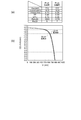
- FIG. 2 is a table and a graph illustrating a first example of the photoelectric conversion element according to the embodiment.
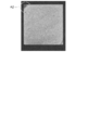
- FIG. 3 shows an EMS (Emission Microscopy) image of the photoelectric conversion element according to the first comparative example.
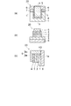
- FIG. 4 is a schematic diagram illustrating a photoelectric conversion element according to a first comparative example.
- FIG. 2 (a) is a table showing the characteristics of the first example and the first comparative example.
- FIG. 2B is a graph illustrating the relationship between voltage and current density. The horizontal axis of the graph shown in FIG. The vertical axis of the graph shown in FIG. 2B represents the current density CD.
- FIG. 4A is a schematic plan view showing the photoelectric conversion element according to the embodiment.
- FIG. 4B is a schematic cross-sectional view taken along a section CC shown in FIG.
- FIG. 4C is a schematic cross-sectional view taken along the section line DD shown in FIG.
- a glass plate is used for the substrate 6 and ITO is used for the first electrode 1.
- PEDOT: PSS is formed as the first buffer layer 2 and LiF is formed as the second buffer layer 4.
- the first buffer layer 2 functions as a hole transport layer.
- the second buffer layer 4 functions as an electron transport layer.
- PTB7 is formed as a p-type organic semiconductor material of the photoelectric conversion layer 3, and [70] PCBM bulk hetero is formed as an n-type organic semiconductor material.
- the solution is CB containing 3% DIO.
- 0.02 nm of LiF is formed by a vapor deposition machine, and as the second electrode 5, 100 nm of AgMg (Mg: 90 wt%) is formed.
- the film thickness of LiF formed here (indicated value of the film thickness meter of the vapor deposition machine) is smaller than the diameter of Li atom 0.34 nm. It is difficult to think of a continuous film, meaning an average film thickness.
- the photoelectric conversion element 20 according to the first comparative example does not have the third buffer layer 7.
- the first buffer layer 2 extends to the end 1 a of the first electrode 1.
- Other structures are the same as those of the photoelectric conversion element 10 according to the first embodiment.
- the conversion efficiency ( ⁇ (%)) of the photoelectric conversion element 20 according to the first comparative example is compared with the conversion efficiency of the photoelectric conversion element 10 according to the first example. It turns out that it is falling.
- region A2 shown in FIG. 3 it can be seen that current leaks at the end 1a of the photoelectric conversion element 20 according to the first comparative example.
- a region A2 illustrated in FIG. 3 corresponds to a region A3 (the end 1a of the first electrode 1) illustrated in FIG.
- the third buffer layer 7 has the end 1a of the first electrode 1 (a portion corresponding to the region A3 shown in FIG. 4C). Is provided. As a result, a decrease in shunt resistance can be suppressed, and current leakage can be suppressed.
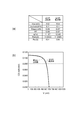
- FIG. 5 is a graph illustrating a second example of the photoelectric conversion element according to the embodiment.
- the structure of the photoelectric conversion element 10 according to the second embodiment is as described above with reference to FIGS. 1 (a) to 1 (b).
- the shape of the photoelectric conversion layer 3 when viewed in the direction of FIG. 1A, the shape of the photoelectric conversion layer 3 is 4.4 millimeters (mm) ⁇ 23 mm, and the first electrode 1 (ITO ) Is set to 4.4 mm. That is, in the photoelectric conversion element 10 according to the first example, the shape of the photoelectric conversion layer 3 and the shape of the first electrode 1 are not square but rectangular (except for a square). Based on the shape of the photoelectric conversion layer 3 and the first electrode 1, the photoelectric conversion element 10 according to the second example having the same configuration as the photoelectric conversion element 10 according to the first example is manufactured.
- the photoelectric conversion element according to the second comparative example has the same structure as the photoelectric conversion element 20 according to the first comparative example. That is, the structure of the photoelectric conversion element according to the second comparative example is as described above with reference to FIGS. 4 (a) to 4 (c).
- the photoelectric conversion layer 3 of the second comparative example has a rectangular shape (excluding a square).
- the first electrode 1 of the second comparative example has a rectangular shape (excluding a square).
- FIG. 5 an example of a result of measuring characteristics generated by incident light of 100 mW / cm 2 at AM 1.5 is shown in FIG. As shown. As shown in FIG. 5, it can be seen that the conversion efficiency of the photoelectric conversion element 10 according to the second example is higher than the conversion efficiency of the photoelectric conversion element according to the second comparative example.
- the photoelectric conversion element 10 according to the second example can suppress the decrease in the shunt resistance and suppress the leakage of the current.
- FIGS. 6 and 7 are a table and a graph for explaining a third example of the photoelectric conversion element according to the embodiment.
- FIG. 6A and FIG. 7A are tables showing the characteristics of the third example and the third comparative example.
- FIG. 6B and FIG. 7B are graphs illustrating the relationship between voltage and current density.
- the horizontal axis of the graphs shown in FIGS. 6B and 7B represents the voltage V.
- the vertical axis of the graphs shown in FIGS. 6B and 7B represents the current density CD.
- the structure of the photoelectric conversion element 10 according to the third embodiment is as described above with reference to FIGS. 1 (a) to 1 (b).
- the first buffer layer 2 is made of ZnO
- the second buffer layer 4 and the third buffer layer 7 are made of V 2 O 5
- the second electrode 5 is made of Ag.
- the first buffer layer 2 functions as an electron transport layer.
- the second buffer layer 4 functions as a hole transport layer.
- the first buffer layer 2 functions as a hole transport layer
- the second buffer layer 4 functions as an electron transport layer.
- the photoelectric conversion element according to the third comparative example has the same structure as the photoelectric conversion element 20 according to the first comparative example. That is, the structure of the photoelectric conversion element according to the third comparative example is as described above with reference to FIGS. 4 (a) to 4 (c).
- the first buffer layer 2 is made of ZnO
- the second buffer layer 4 is made of V 2 O 5
- the second electrode 5 is made of Ag.
- FIG. 10 In the photoelectric conversion element 10 according to the third example and the photoelectric conversion element according to the third comparative example, electrons are extracted from the first electrode 1 and holes are extracted from the second electrode 5.
- FIG. 10 An example of a result of measuring characteristics generated by incident light of 100 mW / cm 2 at AM 1.5 is shown in FIG. It is as having represented to a) and FIG.6 (b).
- FIGS. 7 (a) and 7 (b) an example of the result of measuring the characteristics generated by incident light of indoor light (LED) of 1000 lux (Lux) is as shown in FIGS. 7 (a) and 7 (b).
- the conversion efficiency of the photoelectric conversion element 10 according to the third example is compared with the conversion efficiency of the photoelectric conversion element according to the third comparative example. You can see that it is rising. Thereby, even if the 1st buffer layer 2 is any of a positive hole transport layer and an electron carrying layer, the photoelectric conversion element 10 concerning embodiment can suppress the fall of shunt resistance, and an electric current leaks. That can be suppressed. Moreover, even if the 2nd buffer layer 4 is any of a positive hole transport layer and an electron carrying layer, the photoelectric conversion element 10 concerning embodiment can suppress the fall of shunt resistance, and an electric current leaks. Can be suppressed. According to the embodiment, a photoelectric conversion element that can suppress a decrease in shunt resistance can be provided.
- a photoelectric conversion element capable of suppressing a decrease in shunt resistance.
Landscapes
- Physics & Mathematics (AREA)
- Electromagnetism (AREA)
- Engineering & Computer Science (AREA)
- Power Engineering (AREA)
- Chemical & Material Sciences (AREA)
- Chemical Kinetics & Catalysis (AREA)
- Electrochemistry (AREA)
- Microelectronics & Electronic Packaging (AREA)
- Photovoltaic Devices (AREA)
- Light Receiving Elements (AREA)
- Electroluminescent Light Sources (AREA)
Priority Applications (1)
| Application Number | Priority Date | Filing Date | Title |
|---|---|---|---|
| US15/263,575 US20160379762A1 (en) | 2014-09-22 | 2016-09-13 | Photoelectric conversion element |
Applications Claiming Priority (2)
| Application Number | Priority Date | Filing Date | Title |
|---|---|---|---|
| JP2014-192261 | 2014-09-22 | ||
| JP2014192261A JP6076302B2 (ja) | 2014-09-22 | 2014-09-22 | 光電変換素子 |
Related Child Applications (1)
| Application Number | Title | Priority Date | Filing Date |
|---|---|---|---|
| US15/263,575 Continuation US20160379762A1 (en) | 2014-09-22 | 2016-09-13 | Photoelectric conversion element |
Publications (1)
| Publication Number | Publication Date |
|---|---|
| WO2016047216A1 true WO2016047216A1 (ja) | 2016-03-31 |
Family
ID=55580757
Family Applications (1)
| Application Number | Title | Priority Date | Filing Date |
|---|---|---|---|
| PCT/JP2015/066641 Ceased WO2016047216A1 (ja) | 2014-09-22 | 2015-06-09 | 光電変換素子 |
Country Status (3)
| Country | Link |
|---|---|
| US (1) | US20160379762A1 (enExample) |
| JP (1) | JP6076302B2 (enExample) |
| WO (1) | WO2016047216A1 (enExample) |
Cited By (1)
| Publication number | Priority date | Publication date | Assignee | Title |
|---|---|---|---|---|
| JP2016219793A (ja) * | 2015-05-25 | 2016-12-22 | パナソニック株式会社 | 太陽電池および太陽電池モジュール |
Families Citing this family (3)
| Publication number | Priority date | Publication date | Assignee | Title |
|---|---|---|---|---|
| JP6378383B1 (ja) * | 2017-03-07 | 2018-08-22 | 株式会社東芝 | 半導体素子およびその製造方法 |
| US10553367B2 (en) * | 2017-10-20 | 2020-02-04 | Qatar Foundation | Photovoltaic perovskite oxychalcogenide material and optoelectronic devices including the same |
| JP7745081B2 (ja) * | 2022-03-08 | 2025-09-26 | 株式会社Magnolia White | 検出装置 |
Citations (4)
| Publication number | Priority date | Publication date | Assignee | Title |
|---|---|---|---|---|
| JP2006222384A (ja) * | 2005-02-14 | 2006-08-24 | Matsushita Electric Ind Co Ltd | 集積型薄膜太陽電池及びその製造方法 |
| JP2013069797A (ja) * | 2011-09-21 | 2013-04-18 | Toshiba Corp | 薄膜太陽電池モジュール |
| JP2014017484A (ja) * | 2012-07-06 | 2014-01-30 | Samsung Electronics Co Ltd | 有機光電材料、これを含む有機光電素子、及びイメージセンサー |
| JP2014038975A (ja) * | 2012-08-20 | 2014-02-27 | Idemitsu Kosan Co Ltd | 有機薄膜太陽電池モジュール |
Family Cites Families (14)
| Publication number | Priority date | Publication date | Assignee | Title |
|---|---|---|---|---|
| DE3604917A1 (de) * | 1986-02-17 | 1987-08-27 | Messerschmitt Boelkow Blohm | Verfahren zur herstellung eines integrierten verbandes in reihe geschalteter duennschicht-solarzellen |
| JPS63177476A (ja) * | 1987-01-16 | 1988-07-21 | Sanyo Electric Co Ltd | 光起電力装置の製造方法 |
| JP2986875B2 (ja) * | 1990-09-07 | 1999-12-06 | キヤノン株式会社 | 集積化太陽電池 |
| JPH06291344A (ja) * | 1993-03-31 | 1994-10-18 | Asahi Chem Ind Co Ltd | 光電変換素子集合体 |
| JPH11214719A (ja) * | 1998-01-28 | 1999-08-06 | Citizen Watch Co Ltd | 太陽電池素子の製造方法 |
| JPH11224956A (ja) * | 1998-02-05 | 1999-08-17 | Matsushita Electric Ind Co Ltd | 薄膜太陽電池およびその製造方法 |
| US20070017617A1 (en) * | 2005-07-22 | 2007-01-25 | Lafrique Michel M | Tire with tread of cap/semibase construction |
| CA2662177A1 (en) * | 2006-08-29 | 2008-04-24 | Martin B. Rawls-Meehan | A foam spring mattress configured with variable firmness |
| CN102598339A (zh) * | 2009-10-29 | 2012-07-18 | 住友化学株式会社 | 有机薄膜太阳能电池模块的制造方法 |
| US9059347B2 (en) * | 2010-06-18 | 2015-06-16 | Semiconductor Energy Laboratory Co., Ltd. | Photoelectric conversion device and manufacturing method thereof |
| JP2013026339A (ja) * | 2011-07-19 | 2013-02-04 | Fujifilm Corp | 薄膜太陽電池およびその製造方法 |
| JP2013149699A (ja) * | 2012-01-18 | 2013-08-01 | Fujifilm Corp | 集積化太陽電池の製造方法 |
| JP2013149698A (ja) * | 2012-01-18 | 2013-08-01 | Fujifilm Corp | 集積化太陽電池の製造方法 |
| JP2014041908A (ja) * | 2012-08-22 | 2014-03-06 | Mitsubishi Chemicals Corp | 有機薄膜太陽電池の製造方法 |
-
2014
- 2014-09-22 JP JP2014192261A patent/JP6076302B2/ja active Active
-
2015
- 2015-06-09 WO PCT/JP2015/066641 patent/WO2016047216A1/ja not_active Ceased
-
2016
- 2016-09-13 US US15/263,575 patent/US20160379762A1/en not_active Abandoned
Patent Citations (4)
| Publication number | Priority date | Publication date | Assignee | Title |
|---|---|---|---|---|
| JP2006222384A (ja) * | 2005-02-14 | 2006-08-24 | Matsushita Electric Ind Co Ltd | 集積型薄膜太陽電池及びその製造方法 |
| JP2013069797A (ja) * | 2011-09-21 | 2013-04-18 | Toshiba Corp | 薄膜太陽電池モジュール |
| JP2014017484A (ja) * | 2012-07-06 | 2014-01-30 | Samsung Electronics Co Ltd | 有機光電材料、これを含む有機光電素子、及びイメージセンサー |
| JP2014038975A (ja) * | 2012-08-20 | 2014-02-27 | Idemitsu Kosan Co Ltd | 有機薄膜太陽電池モジュール |
Cited By (1)
| Publication number | Priority date | Publication date | Assignee | Title |
|---|---|---|---|---|
| JP2016219793A (ja) * | 2015-05-25 | 2016-12-22 | パナソニック株式会社 | 太陽電池および太陽電池モジュール |
Also Published As
| Publication number | Publication date |
|---|---|
| JP2016063173A (ja) | 2016-04-25 |
| JP6076302B2 (ja) | 2017-02-08 |
| US20160379762A1 (en) | 2016-12-29 |
Similar Documents
| Publication | Publication Date | Title |
|---|---|---|
| JP5603912B2 (ja) | 太陽電池モジュール | |
| JP5300903B2 (ja) | ポリマーおよびそれを用いた太陽電池、太陽光発電システム | |
| JP6486737B2 (ja) | 光電変換素子 | |
| JP2016058455A (ja) | 光電変換素子、光電変換素子の配線基板、光電変換素子の製造方法、および光電変換構造体 | |
| JP6486719B2 (ja) | 光電変換素子の製造方法 | |
| JP6408042B2 (ja) | 光電変換素子およびその製造方法 | |
| JP6005785B1 (ja) | 光電変換素子およびその製造方法 | |
| JP2011119702A (ja) | 有機光電変換素子 | |
| JP5537636B2 (ja) | 太陽電池及び太陽電池モジュール | |
| JP6076302B2 (ja) | 光電変換素子 | |
| JP6049556B2 (ja) | 太陽電池、太陽電池モジュール及び太陽電池の製造方法 | |
| JP6675505B2 (ja) | 光電変換素子の製造方法 | |
| JP5362017B2 (ja) | 有機薄膜太陽電池 | |
| JP6027641B2 (ja) | 光電変換素子および太陽電池 | |
| JP5932928B2 (ja) | 光電変換装置 | |
| JP5665839B2 (ja) | 太陽電池およびその製造方法 | |
| JP6010649B2 (ja) | 太陽電池モジュールおよびその製造方法 | |
| JP5889998B1 (ja) | 有機薄膜太陽電池 | |
| JP6076392B2 (ja) | 太陽電池モジュールおよびその製造方法 | |
| JP2016066645A (ja) | 光電変換素子および光電変換素子の製造方法 | |
| JP2016100357A (ja) | 光電変換装置 |
Legal Events
| Date | Code | Title | Description |
|---|---|---|---|
| 121 | Ep: the epo has been informed by wipo that ep was designated in this application |
Ref document number: 15843217 Country of ref document: EP Kind code of ref document: A1 |
|
| NENP | Non-entry into the national phase |
Ref country code: DE |
|
| 122 | Ep: pct application non-entry in european phase |
Ref document number: 15843217 Country of ref document: EP Kind code of ref document: A1 |