WO2016047216A1 - Photoelectric conversion element - Google Patents
Photoelectric conversion element Download PDFInfo
- Publication number
- WO2016047216A1 WO2016047216A1 PCT/JP2015/066641 JP2015066641W WO2016047216A1 WO 2016047216 A1 WO2016047216 A1 WO 2016047216A1 JP 2015066641 W JP2015066641 W JP 2015066641W WO 2016047216 A1 WO2016047216 A1 WO 2016047216A1
- Authority
- WO
- WIPO (PCT)
- Prior art keywords
- electrode
- photoelectric conversion
- conversion element
- buffer layer
- element according
- Prior art date
Links
- 238000006243 chemical reaction Methods 0.000 title claims abstract description 142
- 239000010410 layer Substances 0.000 claims description 162
- 239000000463 material Substances 0.000 claims description 58
- 239000004065 semiconductor Substances 0.000 claims description 36
- XMWRBQBLMFGWIX-UHFFFAOYSA-N C60 fullerene Chemical compound C12=C3C(C4=C56)=C7C8=C5C5=C9C%10=C6C6=C4C1=C1C4=C6C6=C%10C%10=C9C9=C%11C5=C8C5=C8C7=C3C3=C7C2=C1C1=C2C4=C6C4=C%10C6=C9C9=C%11C5=C5C8=C3C3=C7C1=C1C2=C4C6=C2C9=C5C3=C12 XMWRBQBLMFGWIX-UHFFFAOYSA-N 0.000 claims description 15
- 229920000123 polythiophene Polymers 0.000 claims description 10
- 239000011521 glass Substances 0.000 claims description 7
- 229910044991 metal oxide Inorganic materials 0.000 claims description 7
- 150000004706 metal oxides Chemical class 0.000 claims description 7
- 229910003472 fullerene Inorganic materials 0.000 claims description 5
- 150000002366 halogen compounds Chemical group 0.000 claims description 5
- 229920000144 PEDOT:PSS Polymers 0.000 claims description 4
- 239000002356 single layer Substances 0.000 claims description 4
- 239000004020 conductor Substances 0.000 claims description 2
- AMGQUBHHOARCQH-UHFFFAOYSA-N indium;oxotin Chemical group [In].[Sn]=O AMGQUBHHOARCQH-UHFFFAOYSA-N 0.000 claims description 2
- 230000000052 comparative effect Effects 0.000 description 26
- 239000000758 substrate Substances 0.000 description 24
- 230000005525 hole transport Effects 0.000 description 18
- 150000002500 ions Chemical class 0.000 description 16
- 239000002904 solvent Substances 0.000 description 13
- 239000010408 film Substances 0.000 description 11
- 238000000576 coating method Methods 0.000 description 10
- 238000000034 method Methods 0.000 description 10
- 230000007423 decrease Effects 0.000 description 9
- XLOMVQKBTHCTTD-UHFFFAOYSA-N Zinc monoxide Chemical compound [Zn]=O XLOMVQKBTHCTTD-UHFFFAOYSA-N 0.000 description 8
- 239000011248 coating agent Substances 0.000 description 7
- 239000007772 electrode material Substances 0.000 description 6
- -1 polyethylene Polymers 0.000 description 6
- MCEWYIDBDVPMES-UHFFFAOYSA-N [60]pcbm Chemical compound C123C(C4=C5C6=C7C8=C9C%10=C%11C%12=C%13C%14=C%15C%16=C%17C%18=C(C=%19C=%20C%18=C%18C%16=C%13C%13=C%11C9=C9C7=C(C=%20C9=C%13%18)C(C7=%19)=C96)C6=C%11C%17=C%15C%13=C%15C%14=C%12C%12=C%10C%10=C85)=C9C7=C6C2=C%11C%13=C2C%15=C%12C%10=C4C23C1(CCCC(=O)OC)C1=CC=CC=C1 MCEWYIDBDVPMES-UHFFFAOYSA-N 0.000 description 5
- 229920001577 copolymer Polymers 0.000 description 5
- 229910045601 alloy Inorganic materials 0.000 description 4
- 239000000956 alloy Substances 0.000 description 4
- 229920001940 conductive polymer Polymers 0.000 description 4
- 125000000524 functional group Chemical group 0.000 description 4
- 229910010272 inorganic material Inorganic materials 0.000 description 4
- 239000011147 inorganic material Substances 0.000 description 4
- 229910052751 metal Inorganic materials 0.000 description 4
- 239000002184 metal Substances 0.000 description 4
- BASFCYQUMIYNBI-UHFFFAOYSA-N platinum Chemical compound [Pt] BASFCYQUMIYNBI-UHFFFAOYSA-N 0.000 description 4
- 238000004528 spin coating Methods 0.000 description 4
- 239000010409 thin film Substances 0.000 description 4
- 239000011787 zinc oxide Substances 0.000 description 4
- 229910000838 Al alloy Inorganic materials 0.000 description 3
- YMWUJEATGCHHMB-UHFFFAOYSA-N Dichloromethane Chemical compound ClCCl YMWUJEATGCHHMB-UHFFFAOYSA-N 0.000 description 3
- 229920001609 Poly(3,4-ethylenedioxythiophene) Polymers 0.000 description 3
- YTPLMLYBLZKORZ-UHFFFAOYSA-N Thiophene Chemical group C=1C=CSC=1 YTPLMLYBLZKORZ-UHFFFAOYSA-N 0.000 description 3
- GWEVSGVZZGPLCZ-UHFFFAOYSA-N Titan oxide Chemical compound O=[Ti]=O GWEVSGVZZGPLCZ-UHFFFAOYSA-N 0.000 description 3
- YXFVVABEGXRONW-UHFFFAOYSA-N Toluene Chemical compound CC1=CC=CC=C1 YXFVVABEGXRONW-UHFFFAOYSA-N 0.000 description 3
- 229910052802 copper Inorganic materials 0.000 description 3
- 239000010949 copper Substances 0.000 description 3
- 229910052737 gold Inorganic materials 0.000 description 3
- 239000010931 gold Substances 0.000 description 3
- 229920000767 polyaniline Polymers 0.000 description 3
- 238000007639 printing Methods 0.000 description 3
- 229910052709 silver Inorganic materials 0.000 description 3
- CXWXQJXEFPUFDZ-UHFFFAOYSA-N tetralin Chemical compound C1=CC=C2CCCCC2=C1 CXWXQJXEFPUFDZ-UHFFFAOYSA-N 0.000 description 3
- OGIDPMRJRNCKJF-UHFFFAOYSA-N titanium oxide Inorganic materials [Ti]=O OGIDPMRJRNCKJF-UHFFFAOYSA-N 0.000 description 3
- 238000007740 vapor deposition Methods 0.000 description 3
- SOXJIUQYIXEZLL-UHFFFAOYSA-N 3-phenylthiophene Chemical compound S1[C]=CC(C=2C=CC=CC=2)=C1 SOXJIUQYIXEZLL-UHFFFAOYSA-N 0.000 description 2
- UJOBWOGCFQCDNV-UHFFFAOYSA-N 9H-carbazole Chemical compound C1=CC=C2C3=CC=CC=C3NC2=C1 UJOBWOGCFQCDNV-UHFFFAOYSA-N 0.000 description 2
- 239000005964 Acibenzolar-S-methyl Substances 0.000 description 2
- 229910001316 Ag alloy Inorganic materials 0.000 description 2
- ATLMFJTZZPOKLC-UHFFFAOYSA-N C70 fullerene Chemical compound C12=C(C3=C4C5=C67)C8=C9C%10=C%11C%12=C%13C(C%14=C%15C%16=%17)=C%18C%19=C%20C%21=C%22C%23=C%24C%21=C%21C(C=%25%26)=C%20C%18=C%12C%26=C%10C8=C4C=%25C%21=C5C%24=C6C(C4=C56)=C%23C5=C5C%22=C%19C%14=C5C=%17C6=C5C6=C4C7=C3C1=C6C1=C5C%16=C3C%15=C%13C%11=C4C9=C2C1=C34 ATLMFJTZZPOKLC-UHFFFAOYSA-N 0.000 description 2
- HEDRZPFGACZZDS-UHFFFAOYSA-N Chloroform Chemical compound ClC(Cl)Cl HEDRZPFGACZZDS-UHFFFAOYSA-N 0.000 description 2
- RYGMFSIKBFXOCR-UHFFFAOYSA-N Copper Chemical compound [Cu] RYGMFSIKBFXOCR-UHFFFAOYSA-N 0.000 description 2
- 229910000846 In alloy Inorganic materials 0.000 description 2
- PXHVJJICTQNCMI-UHFFFAOYSA-N Nickel Chemical compound [Ni] PXHVJJICTQNCMI-UHFFFAOYSA-N 0.000 description 2
- BQCADISMDOOEFD-UHFFFAOYSA-N Silver Chemical compound [Ag] BQCADISMDOOEFD-UHFFFAOYSA-N 0.000 description 2
- FAPWRFPIFSIZLT-UHFFFAOYSA-M Sodium chloride Chemical compound [Na+].[Cl-] FAPWRFPIFSIZLT-UHFFFAOYSA-M 0.000 description 2
- WYURNTSHIVDZCO-UHFFFAOYSA-N Tetrahydrofuran Chemical compound C1CCOC1 WYURNTSHIVDZCO-UHFFFAOYSA-N 0.000 description 2
- 125000003342 alkenyl group Chemical group 0.000 description 2
- 125000003545 alkoxy group Chemical group 0.000 description 2
- 125000000217 alkyl group Chemical group 0.000 description 2
- 150000004982 aromatic amines Chemical class 0.000 description 2
- 125000006615 aromatic heterocyclic group Chemical group 0.000 description 2
- 125000002029 aromatic hydrocarbon group Chemical group 0.000 description 2
- 150000004945 aromatic hydrocarbons Chemical class 0.000 description 2
- OCKPCBLVNKHBMX-UHFFFAOYSA-N butylbenzene Chemical compound CCCCC1=CC=CC=C1 OCKPCBLVNKHBMX-UHFFFAOYSA-N 0.000 description 2
- 229910052791 calcium Inorganic materials 0.000 description 2
- 239000011575 calcium Substances 0.000 description 2
- 229910052801 chlorine Inorganic materials 0.000 description 2
- MVPPADPHJFYWMZ-UHFFFAOYSA-N chlorobenzene Chemical compound ClC1=CC=CC=C1 MVPPADPHJFYWMZ-UHFFFAOYSA-N 0.000 description 2
- 150000001875 compounds Chemical class 0.000 description 2
- 239000013078 crystal Substances 0.000 description 2
- NNBZCPXTIHJBJL-UHFFFAOYSA-N decalin Chemical compound C1CCCC2CCCCC21 NNBZCPXTIHJBJL-UHFFFAOYSA-N 0.000 description 2
- 238000010586 diagram Methods 0.000 description 2
- 150000002170 ethers Chemical class 0.000 description 2
- PCHJSUWPFVWCPO-UHFFFAOYSA-N gold Chemical compound [Au] PCHJSUWPFVWCPO-UHFFFAOYSA-N 0.000 description 2
- 125000005843 halogen group Chemical group 0.000 description 2
- 229910052744 lithium Inorganic materials 0.000 description 2
- AMXOYNBUYSYVKV-UHFFFAOYSA-M lithium bromide Chemical compound [Li+].[Br-] AMXOYNBUYSYVKV-UHFFFAOYSA-M 0.000 description 2
- KWGKDLIKAYFUFQ-UHFFFAOYSA-M lithium chloride Chemical compound [Li+].[Cl-] KWGKDLIKAYFUFQ-UHFFFAOYSA-M 0.000 description 2
- PQXKHYXIUOZZFA-UHFFFAOYSA-M lithium fluoride Chemical compound [Li+].[F-] PQXKHYXIUOZZFA-UHFFFAOYSA-M 0.000 description 2
- 229910000476 molybdenum oxide Inorganic materials 0.000 description 2
- 238000007645 offset printing Methods 0.000 description 2
- PQQKPALAQIIWST-UHFFFAOYSA-N oxomolybdenum Chemical compound [Mo]=O PQQKPALAQIIWST-UHFFFAOYSA-N 0.000 description 2
- 239000004033 plastic Substances 0.000 description 2
- 229910052697 platinum Inorganic materials 0.000 description 2
- 229920000139 polyethylene terephthalate Polymers 0.000 description 2
- 239000005020 polyethylene terephthalate Substances 0.000 description 2
- 229920000642 polymer Polymers 0.000 description 2
- 229920006254 polymer film Polymers 0.000 description 2
- 229920000128 polypyrrole Polymers 0.000 description 2
- 229930195734 saturated hydrocarbon Natural products 0.000 description 2
- 238000000926 separation method Methods 0.000 description 2
- 239000004332 silver Substances 0.000 description 2
- JHJLBTNAGRQEKS-UHFFFAOYSA-M sodium bromide Chemical compound [Na+].[Br-] JHJLBTNAGRQEKS-UHFFFAOYSA-M 0.000 description 2
- PUZPDOWCWNUUKD-UHFFFAOYSA-M sodium fluoride Chemical compound [F-].[Na+] PUZPDOWCWNUUKD-UHFFFAOYSA-M 0.000 description 2
- FVAUCKIRQBBSSJ-UHFFFAOYSA-M sodium iodide Chemical compound [Na+].[I-] FVAUCKIRQBBSSJ-UHFFFAOYSA-M 0.000 description 2
- 238000004544 sputter deposition Methods 0.000 description 2
- YTZKOQUCBOVLHL-UHFFFAOYSA-N tert-butylbenzene Chemical compound CC(C)(C)C1=CC=CC=C1 YTZKOQUCBOVLHL-UHFFFAOYSA-N 0.000 description 2
- VZGDMQKNWNREIO-UHFFFAOYSA-N tetrachloromethane Chemical compound ClC(Cl)(Cl)Cl VZGDMQKNWNREIO-UHFFFAOYSA-N 0.000 description 2
- 229910052718 tin Inorganic materials 0.000 description 2
- 239000011135 tin Substances 0.000 description 2
- XOLBLPGZBRYERU-UHFFFAOYSA-N tin dioxide Chemical compound O=[Sn]=O XOLBLPGZBRYERU-UHFFFAOYSA-N 0.000 description 2
- 229910001887 tin oxide Inorganic materials 0.000 description 2
- 229910052719 titanium Inorganic materials 0.000 description 2
- 239000010936 titanium Substances 0.000 description 2
- 229930195735 unsaturated hydrocarbon Natural products 0.000 description 2
- SCYULBFZEHDVBN-UHFFFAOYSA-N 1,1-Dichloroethane Chemical compound CC(Cl)Cl SCYULBFZEHDVBN-UHFFFAOYSA-N 0.000 description 1
- FNQJDLTXOVEEFB-UHFFFAOYSA-N 1,2,3-benzothiadiazole Chemical compound C1=CC=C2SN=NC2=C1 FNQJDLTXOVEEFB-UHFFFAOYSA-N 0.000 description 1
- RELMFMZEBKVZJC-UHFFFAOYSA-N 1,2,3-trichlorobenzene Chemical compound ClC1=CC=CC(Cl)=C1Cl RELMFMZEBKVZJC-UHFFFAOYSA-N 0.000 description 1
- OCJBOOLMMGQPQU-UHFFFAOYSA-N 1,4-dichlorobenzene Chemical compound ClC1=CC=C(Cl)C=C1 OCJBOOLMMGQPQU-UHFFFAOYSA-N 0.000 description 1
- MPPPKRYCTPRNTB-UHFFFAOYSA-N 1-bromobutane Chemical compound CCCCBr MPPPKRYCTPRNTB-UHFFFAOYSA-N 0.000 description 1
- MNDIARAMWBIKFW-UHFFFAOYSA-N 1-bromohexane Chemical compound CCCCCCBr MNDIARAMWBIKFW-UHFFFAOYSA-N 0.000 description 1
- VFWCMGCRMGJXDK-UHFFFAOYSA-N 1-chlorobutane Chemical compound CCCCCl VFWCMGCRMGJXDK-UHFFFAOYSA-N 0.000 description 1
- MLRVZFYXUZQSRU-UHFFFAOYSA-N 1-chlorohexane Chemical compound CCCCCCCl MLRVZFYXUZQSRU-UHFFFAOYSA-N 0.000 description 1
- SQCZQTSHSZLZIQ-UHFFFAOYSA-N 1-chloropentane Chemical compound CCCCCCl SQCZQTSHSZLZIQ-UHFFFAOYSA-N 0.000 description 1
- QENGPZGAWFQWCZ-UHFFFAOYSA-N 3-Methylthiophene Chemical compound CC=1C=CSC=1 QENGPZGAWFQWCZ-UHFFFAOYSA-N 0.000 description 1
- BZORYGRKQHUBCY-UHFFFAOYSA-N 3-butylthiophene Chemical compound [CH2]CCCC=1C=CSC=1 BZORYGRKQHUBCY-UHFFFAOYSA-N 0.000 description 1
- JAYBIBLZTQMCAY-UHFFFAOYSA-N 3-decylthiophene Chemical compound CCCCCCCCCCC=1C=CSC=1 JAYBIBLZTQMCAY-UHFFFAOYSA-N 0.000 description 1
- RFKWIEFTBMACPZ-UHFFFAOYSA-N 3-dodecylthiophene Chemical compound CCCCCCCCCCCCC=1C=CSC=1 RFKWIEFTBMACPZ-UHFFFAOYSA-N 0.000 description 1
- WQYWXQCOYRZFAV-UHFFFAOYSA-N 3-octylthiophene Chemical compound CCCCCCCCC=1C=CSC=1 WQYWXQCOYRZFAV-UHFFFAOYSA-N 0.000 description 1
- CMSGUKVDXXTJDQ-UHFFFAOYSA-N 4-(2-naphthalen-1-ylethylamino)-4-oxobutanoic acid Chemical compound C1=CC=C2C(CCNC(=O)CCC(=O)O)=CC=CC2=C1 CMSGUKVDXXTJDQ-UHFFFAOYSA-N 0.000 description 1
- AZSFNTBGCTUQFX-UHFFFAOYSA-N C12=C3C(C4=C5C=6C7=C8C9=C(C%10=6)C6=C%11C=%12C%13=C%14C%11=C9C9=C8C8=C%11C%15=C%16C=%17C(C=%18C%19=C4C7=C8C%15=%18)=C4C7=C8C%15=C%18C%20=C(C=%178)C%16=C8C%11=C9C%14=C8C%20=C%13C%18=C8C9=%12)=C%19C4=C2C7=C2C%15=C8C=4C2=C1C12C3=C5C%10=C3C6=C9C=4C32C1(CCCC(=O)OC)C1=CC=CC=C1 Chemical compound C12=C3C(C4=C5C=6C7=C8C9=C(C%10=6)C6=C%11C=%12C%13=C%14C%11=C9C9=C8C8=C%11C%15=C%16C=%17C(C=%18C%19=C4C7=C8C%15=%18)=C4C7=C8C%15=C%18C%20=C(C=%178)C%16=C8C%11=C9C%14=C8C%20=C%13C%18=C8C9=%12)=C%19C4=C2C7=C2C%15=C8C=4C2=C1C12C3=C5C%10=C3C6=C9C=4C32C1(CCCC(=O)OC)C1=CC=CC=C1 AZSFNTBGCTUQFX-UHFFFAOYSA-N 0.000 description 1
- OYPRJOBELJOOCE-UHFFFAOYSA-N Calcium Chemical compound [Ca] OYPRJOBELJOOCE-UHFFFAOYSA-N 0.000 description 1
- 229920000089 Cyclic olefin copolymer Polymers 0.000 description 1
- 229920000106 Liquid crystal polymer Polymers 0.000 description 1
- 239000004977 Liquid-crystal polymers (LCPs) Substances 0.000 description 1
- 229910000861 Mg alloy Inorganic materials 0.000 description 1
- CTQNGGLPUBDAKN-UHFFFAOYSA-N O-Xylene Chemical compound CC1=CC=CC=C1C CTQNGGLPUBDAKN-UHFFFAOYSA-N 0.000 description 1
- 239000004952 Polyamide Substances 0.000 description 1
- 239000004962 Polyamide-imide Substances 0.000 description 1
- 239000004698 Polyethylene Substances 0.000 description 1
- 239000004642 Polyimide Substances 0.000 description 1
- VYPSYNLAJGMNEJ-UHFFFAOYSA-N Silicium dioxide Chemical compound O=[Si]=O VYPSYNLAJGMNEJ-UHFFFAOYSA-N 0.000 description 1
- 229910052771 Terbium Inorganic materials 0.000 description 1
- DHXVGJBLRPWPCS-UHFFFAOYSA-N Tetrahydropyran Chemical compound C1CCOCC1 DHXVGJBLRPWPCS-UHFFFAOYSA-N 0.000 description 1
- ATJFFYVFTNAWJD-UHFFFAOYSA-N Tin Chemical compound [Sn] ATJFFYVFTNAWJD-UHFFFAOYSA-N 0.000 description 1
- RTAQQCXQSZGOHL-UHFFFAOYSA-N Titanium Chemical compound [Ti] RTAQQCXQSZGOHL-UHFFFAOYSA-N 0.000 description 1
- 229910052769 Ytterbium Inorganic materials 0.000 description 1
- ULGYAEQHFNJYML-UHFFFAOYSA-N [AlH3].[Ca] Chemical compound [AlH3].[Ca] ULGYAEQHFNJYML-UHFFFAOYSA-N 0.000 description 1
- JFBZPFYRPYOZCQ-UHFFFAOYSA-N [Li].[Al] Chemical compound [Li].[Al] JFBZPFYRPYOZCQ-UHFFFAOYSA-N 0.000 description 1
- XHCLAFWTIXFWPH-UHFFFAOYSA-N [O-2].[O-2].[O-2].[O-2].[O-2].[V+5].[V+5] Chemical compound [O-2].[O-2].[O-2].[O-2].[O-2].[V+5].[V+5] XHCLAFWTIXFWPH-UHFFFAOYSA-N 0.000 description 1
- 229910052783 alkali metal Inorganic materials 0.000 description 1
- 150000001340 alkali metals Chemical class 0.000 description 1
- 229910052784 alkaline earth metal Inorganic materials 0.000 description 1
- 150000001342 alkaline earth metals Chemical class 0.000 description 1
- 229910052782 aluminium Inorganic materials 0.000 description 1
- SNAAJJQQZSMGQD-UHFFFAOYSA-N aluminum magnesium Chemical compound [Mg].[Al] SNAAJJQQZSMGQD-UHFFFAOYSA-N 0.000 description 1
- 239000003849 aromatic solvent Substances 0.000 description 1
- 125000004429 atom Chemical group 0.000 description 1
- 229910052788 barium Inorganic materials 0.000 description 1
- 239000002585 base Substances 0.000 description 1
- 230000015572 biosynthetic process Effects 0.000 description 1
- 230000000903 blocking effect Effects 0.000 description 1
- 229910052794 bromium Inorganic materials 0.000 description 1
- 229910052792 caesium Inorganic materials 0.000 description 1
- KOPBYBDAPCDYFK-UHFFFAOYSA-N caesium oxide Chemical compound [O-2].[Cs+].[Cs+] KOPBYBDAPCDYFK-UHFFFAOYSA-N 0.000 description 1
- 229910001942 caesium oxide Inorganic materials 0.000 description 1
- GMYSDEOJMBLAKZ-UHFFFAOYSA-N calcium indium Chemical compound [Ca].[In] GMYSDEOJMBLAKZ-UHFFFAOYSA-N 0.000 description 1
- BRPQOXSCLDDYGP-UHFFFAOYSA-N calcium oxide Chemical compound [O-2].[Ca+2] BRPQOXSCLDDYGP-UHFFFAOYSA-N 0.000 description 1
- ODINCKMPIJJUCX-UHFFFAOYSA-N calcium oxide Inorganic materials [Ca]=O ODINCKMPIJJUCX-UHFFFAOYSA-N 0.000 description 1
- 239000000292 calcium oxide Substances 0.000 description 1
- 125000004432 carbon atom Chemical group C* 0.000 description 1
- 238000005266 casting Methods 0.000 description 1
- 230000008859 change Effects 0.000 description 1
- 239000000460 chlorine Substances 0.000 description 1
- 125000001309 chloro group Chemical group Cl* 0.000 description 1
- 229910017052 cobalt Inorganic materials 0.000 description 1
- 239000010941 cobalt Substances 0.000 description 1
- GUTLYIVDDKVIGB-UHFFFAOYSA-N cobalt atom Chemical compound [Co] GUTLYIVDDKVIGB-UHFFFAOYSA-N 0.000 description 1
- 239000002131 composite material Substances 0.000 description 1
- 239000012141 concentrate Substances 0.000 description 1
- 230000021615 conjugation Effects 0.000 description 1
- 239000000470 constituent Substances 0.000 description 1
- 125000004093 cyano group Chemical group *C#N 0.000 description 1
- 229940117389 dichlorobenzene Drugs 0.000 description 1
- 238000003618 dip coating Methods 0.000 description 1
- 230000000694 effects Effects 0.000 description 1
- 230000005684 electric field Effects 0.000 description 1
- 230000005611 electricity Effects 0.000 description 1
- 125000005678 ethenylene group Chemical group [H]C([*:1])=C([H])[*:2] 0.000 description 1
- 125000001301 ethoxy group Chemical group [H]C([H])([H])C([H])([H])O* 0.000 description 1
- 125000001495 ethyl group Chemical group [H]C([H])([H])C([H])([H])* 0.000 description 1
- 229910052731 fluorine Inorganic materials 0.000 description 1
- 125000001153 fluoro group Chemical group F* 0.000 description 1
- 238000007646 gravure printing Methods 0.000 description 1
- 229910052736 halogen Inorganic materials 0.000 description 1
- 150000002367 halogens Chemical class 0.000 description 1
- 125000005842 heteroatom Chemical group 0.000 description 1
- 125000004435 hydrogen atom Chemical group [H]* 0.000 description 1
- 230000007062 hydrolysis Effects 0.000 description 1
- 238000006460 hydrolysis reaction Methods 0.000 description 1
- 230000003301 hydrolyzing effect Effects 0.000 description 1
- 125000002887 hydroxy group Chemical group [H]O* 0.000 description 1
- 229910052738 indium Inorganic materials 0.000 description 1
- LHJOPRPDWDXEIY-UHFFFAOYSA-N indium lithium Chemical compound [Li].[In] LHJOPRPDWDXEIY-UHFFFAOYSA-N 0.000 description 1
- 229910003437 indium oxide Inorganic materials 0.000 description 1
- YZASAXHKAQYPEH-UHFFFAOYSA-N indium silver Chemical compound [Ag].[In] YZASAXHKAQYPEH-UHFFFAOYSA-N 0.000 description 1
- PJXISJQVUVHSOJ-UHFFFAOYSA-N indium(iii) oxide Chemical compound [O-2].[O-2].[O-2].[In+3].[In+3] PJXISJQVUVHSOJ-UHFFFAOYSA-N 0.000 description 1
- 230000003993 interaction Effects 0.000 description 1
- 229910052740 iodine Inorganic materials 0.000 description 1
- 238000007733 ion plating Methods 0.000 description 1
- 229910052745 lead Inorganic materials 0.000 description 1
- HSZCZNFXUDYRKD-UHFFFAOYSA-M lithium iodide Inorganic materials [Li+].[I-] HSZCZNFXUDYRKD-UHFFFAOYSA-M 0.000 description 1
- GCICAPWZNUIIDV-UHFFFAOYSA-N lithium magnesium Chemical compound [Li].[Mg] GCICAPWZNUIIDV-UHFFFAOYSA-N 0.000 description 1
- FUJCRWPEOMXPAD-UHFFFAOYSA-N lithium oxide Chemical compound [Li+].[Li+].[O-2] FUJCRWPEOMXPAD-UHFFFAOYSA-N 0.000 description 1
- 229910001947 lithium oxide Inorganic materials 0.000 description 1
- 239000011777 magnesium Substances 0.000 description 1
- SJCKRGFTWFGHGZ-UHFFFAOYSA-N magnesium silver Chemical compound [Mg].[Ag] SJCKRGFTWFGHGZ-UHFFFAOYSA-N 0.000 description 1
- WPBNNNQJVZRUHP-UHFFFAOYSA-L manganese(2+);methyl n-[[2-(methoxycarbonylcarbamothioylamino)phenyl]carbamothioyl]carbamate;n-[2-(sulfidocarbothioylamino)ethyl]carbamodithioate Chemical compound [Mn+2].[S-]C(=S)NCCNC([S-])=S.COC(=O)NC(=S)NC1=CC=CC=C1NC(=S)NC(=O)OC WPBNNNQJVZRUHP-UHFFFAOYSA-L 0.000 description 1
- AUHZEENZYGFFBQ-UHFFFAOYSA-N mesitylene Substances CC1=CC(C)=CC(C)=C1 AUHZEENZYGFFBQ-UHFFFAOYSA-N 0.000 description 1
- 125000001827 mesitylenyl group Chemical group [H]C1=C(C(*)=C(C([H])=C1C([H])([H])[H])C([H])([H])[H])C([H])([H])[H] 0.000 description 1
- 150000002739 metals Chemical class 0.000 description 1
- 125000000956 methoxy group Chemical group [H]C([H])([H])O* 0.000 description 1
- 125000002496 methyl group Chemical group [H]C([H])([H])* 0.000 description 1
- 238000000386 microscopy Methods 0.000 description 1
- 238000012986 modification Methods 0.000 description 1
- 230000004048 modification Effects 0.000 description 1
- UNFUYWDGSFDHCW-UHFFFAOYSA-N monochlorocyclohexane Chemical compound ClC1CCCCC1 UNFUYWDGSFDHCW-UHFFFAOYSA-N 0.000 description 1
- DCZNSJVFOQPSRV-UHFFFAOYSA-N n,n-diphenyl-4-[4-(n-phenylanilino)phenyl]aniline Chemical class C1=CC=CC=C1N(C=1C=CC(=CC=1)C=1C=CC(=CC=1)N(C=1C=CC=CC=1)C=1C=CC=CC=1)C1=CC=CC=C1 DCZNSJVFOQPSRV-UHFFFAOYSA-N 0.000 description 1
- 125000001624 naphthyl group Chemical group 0.000 description 1
- 229910052759 nickel Inorganic materials 0.000 description 1
- 229910000480 nickel oxide Inorganic materials 0.000 description 1
- 230000003287 optical effect Effects 0.000 description 1
- 239000003960 organic solvent Substances 0.000 description 1
- TWNQGVIAIRXVLR-UHFFFAOYSA-N oxo(oxoalumanyloxy)alumane Chemical compound O=[Al]O[Al]=O TWNQGVIAIRXVLR-UHFFFAOYSA-N 0.000 description 1
- GNRSAWUEBMWBQH-UHFFFAOYSA-N oxonickel Chemical compound [Ni]=O GNRSAWUEBMWBQH-UHFFFAOYSA-N 0.000 description 1
- 125000001997 phenyl group Chemical group [H]C1=C([H])C([H])=C(*)C([H])=C1[H] 0.000 description 1
- IEQIEDJGQAUEQZ-UHFFFAOYSA-N phthalocyanine Chemical class N1C(N=C2C3=CC=CC=C3C(N=C3C4=CC=CC=C4C(=N4)N3)=N2)=C(C=CC=C2)C2=C1N=C1C2=CC=CC=C2C4=N1 IEQIEDJGQAUEQZ-UHFFFAOYSA-N 0.000 description 1
- 229920003023 plastic Polymers 0.000 description 1
- 229920006255 plastic film Polymers 0.000 description 1
- 238000007747 plating Methods 0.000 description 1
- 229920002848 poly(3-alkoxythiophenes) Polymers 0.000 description 1
- 229920000301 poly(3-hexylthiophene-2,5-diyl) polymer Polymers 0.000 description 1
- 229920003227 poly(N-vinyl carbazole) Polymers 0.000 description 1
- 229920000553 poly(phenylenevinylene) Polymers 0.000 description 1
- 229920000548 poly(silane) polymer Polymers 0.000 description 1
- 229920001467 poly(styrenesulfonates) Polymers 0.000 description 1
- 229920002647 polyamide Polymers 0.000 description 1
- 229920002312 polyamide-imide Polymers 0.000 description 1
- 229920000573 polyethylene Polymers 0.000 description 1
- 239000011112 polyethylene naphthalate Substances 0.000 description 1
- 229920001721 polyimide Polymers 0.000 description 1
- 229920001296 polysiloxane Polymers 0.000 description 1
- 150000004032 porphyrins Chemical class 0.000 description 1
- 229910052700 potassium Inorganic materials 0.000 description 1
- 230000001737 promoting effect Effects 0.000 description 1
- 150000003219 pyrazolines Chemical class 0.000 description 1
- 125000004076 pyridyl group Chemical group 0.000 description 1
- 238000012827 research and development Methods 0.000 description 1
- 230000000630 rising effect Effects 0.000 description 1
- 229910052701 rubidium Inorganic materials 0.000 description 1
- 238000007650 screen-printing Methods 0.000 description 1
- ZJMWRROPUADPEA-UHFFFAOYSA-N sec-butylbenzene Chemical compound CCC(C)C1=CC=CC=C1 ZJMWRROPUADPEA-UHFFFAOYSA-N 0.000 description 1
- 229910052710 silicon Inorganic materials 0.000 description 1
- 239000010703 silicon Substances 0.000 description 1
- 239000010944 silver (metal) Substances 0.000 description 1
- 229910052708 sodium Inorganic materials 0.000 description 1
- 239000011780 sodium chloride Substances 0.000 description 1
- 238000003980 solgel method Methods 0.000 description 1
- 238000005507 spraying Methods 0.000 description 1
- 239000010935 stainless steel Substances 0.000 description 1
- 229910001220 stainless steel Inorganic materials 0.000 description 1
- PJANXHGTPQOBST-UHFFFAOYSA-N stilbene Chemical class C=1C=CC=CC=1C=CC1=CC=CC=C1 PJANXHGTPQOBST-UHFFFAOYSA-N 0.000 description 1
- 239000000126 substance Substances 0.000 description 1
- YLQBMQCUIZJEEH-UHFFFAOYSA-N tetrahydrofuran Natural products C=1C=COC=1 YLQBMQCUIZJEEH-UHFFFAOYSA-N 0.000 description 1
- 125000001544 thienyl group Chemical group 0.000 description 1
- 229930192474 thiophene Natural products 0.000 description 1
- 230000007704 transition Effects 0.000 description 1
- WFKWXMTUELFFGS-UHFFFAOYSA-N tungsten Chemical compound [W] WFKWXMTUELFFGS-UHFFFAOYSA-N 0.000 description 1
- 229910052721 tungsten Inorganic materials 0.000 description 1
- 239000010937 tungsten Substances 0.000 description 1
- 238000001771 vacuum deposition Methods 0.000 description 1
- 229910001935 vanadium oxide Inorganic materials 0.000 description 1
- PXXNTAGJWPJAGM-UHFFFAOYSA-N vertaline Natural products C1C2C=3C=C(OC)C(OC)=CC=3OC(C=C3)=CC=C3CCC(=O)OC1CC1N2CCCC1 PXXNTAGJWPJAGM-UHFFFAOYSA-N 0.000 description 1
- 125000000391 vinyl group Chemical group [H]C([*])=C([H])[H] 0.000 description 1
- 239000008096 xylene Substances 0.000 description 1
- YVTHLONGBIQYBO-UHFFFAOYSA-N zinc indium(3+) oxygen(2-) Chemical compound [O--].[Zn++].[In+3] YVTHLONGBIQYBO-UHFFFAOYSA-N 0.000 description 1
- 229910052726 zirconium Inorganic materials 0.000 description 1
Images


Classifications
-
- H—ELECTRICITY
- H01—ELECTRIC ELEMENTS
- H01G—CAPACITORS; CAPACITORS, RECTIFIERS, DETECTORS, SWITCHING DEVICES, LIGHT-SENSITIVE OR TEMPERATURE-SENSITIVE DEVICES OF THE ELECTROLYTIC TYPE
- H01G9/00—Electrolytic capacitors, rectifiers, detectors, switching devices, light-sensitive or temperature-sensitive devices; Processes of their manufacture
- H01G9/20—Light-sensitive devices
- H01G9/2004—Light-sensitive devices characterised by the electrolyte, e.g. comprising an organic electrolyte
- H01G9/2018—Light-sensitive devices characterised by the electrolyte, e.g. comprising an organic electrolyte characterised by the ionic charge transport species, e.g. redox shuttles
-
- H—ELECTRICITY
- H10—SEMICONDUCTOR DEVICES; ELECTRIC SOLID-STATE DEVICES NOT OTHERWISE PROVIDED FOR
- H10K—ORGANIC ELECTRIC SOLID-STATE DEVICES
- H10K30/00—Organic devices sensitive to infrared radiation, light, electromagnetic radiation of shorter wavelength or corpuscular radiation
- H10K30/30—Organic devices sensitive to infrared radiation, light, electromagnetic radiation of shorter wavelength or corpuscular radiation comprising bulk heterojunctions, e.g. interpenetrating networks of donor and acceptor material domains
- H10K30/353—Organic devices sensitive to infrared radiation, light, electromagnetic radiation of shorter wavelength or corpuscular radiation comprising bulk heterojunctions, e.g. interpenetrating networks of donor and acceptor material domains comprising blocking layers, e.g. exciton blocking layers
-
- H—ELECTRICITY
- H10—SEMICONDUCTOR DEVICES; ELECTRIC SOLID-STATE DEVICES NOT OTHERWISE PROVIDED FOR
- H10K—ORGANIC ELECTRIC SOLID-STATE DEVICES
- H10K30/00—Organic devices sensitive to infrared radiation, light, electromagnetic radiation of shorter wavelength or corpuscular radiation
- H10K30/80—Constructional details
- H10K30/81—Electrodes
- H10K30/82—Transparent electrodes, e.g. indium tin oxide [ITO] electrodes
-
- H—ELECTRICITY
- H10—SEMICONDUCTOR DEVICES; ELECTRIC SOLID-STATE DEVICES NOT OTHERWISE PROVIDED FOR
- H10K—ORGANIC ELECTRIC SOLID-STATE DEVICES
- H10K30/00—Organic devices sensitive to infrared radiation, light, electromagnetic radiation of shorter wavelength or corpuscular radiation
- H10K30/50—Photovoltaic [PV] devices
-
- H—ELECTRICITY
- H10—SEMICONDUCTOR DEVICES; ELECTRIC SOLID-STATE DEVICES NOT OTHERWISE PROVIDED FOR
- H10K—ORGANIC ELECTRIC SOLID-STATE DEVICES
- H10K85/00—Organic materials used in the body or electrodes of devices covered by this subclass
- H10K85/10—Organic polymers or oligomers
- H10K85/111—Organic polymers or oligomers comprising aromatic, heteroaromatic, or aryl chains, e.g. polyaniline, polyphenylene or polyphenylene vinylene
- H10K85/113—Heteroaromatic compounds comprising sulfur or selene, e.g. polythiophene
- H10K85/1135—Polyethylene dioxythiophene [PEDOT]; Derivatives thereof
-
- H—ELECTRICITY
- H10—SEMICONDUCTOR DEVICES; ELECTRIC SOLID-STATE DEVICES NOT OTHERWISE PROVIDED FOR
- H10K—ORGANIC ELECTRIC SOLID-STATE DEVICES
- H10K85/00—Organic materials used in the body or electrodes of devices covered by this subclass
- H10K85/10—Organic polymers or oligomers
- H10K85/151—Copolymers
-
- H—ELECTRICITY
- H10—SEMICONDUCTOR DEVICES; ELECTRIC SOLID-STATE DEVICES NOT OTHERWISE PROVIDED FOR
- H10K—ORGANIC ELECTRIC SOLID-STATE DEVICES
- H10K85/00—Organic materials used in the body or electrodes of devices covered by this subclass
- H10K85/20—Carbon compounds, e.g. carbon nanotubes or fullerenes
- H10K85/211—Fullerenes, e.g. C60
- H10K85/215—Fullerenes, e.g. C60 comprising substituents, e.g. PCBM
-
- Y—GENERAL TAGGING OF NEW TECHNOLOGICAL DEVELOPMENTS; GENERAL TAGGING OF CROSS-SECTIONAL TECHNOLOGIES SPANNING OVER SEVERAL SECTIONS OF THE IPC; TECHNICAL SUBJECTS COVERED BY FORMER USPC CROSS-REFERENCE ART COLLECTIONS [XRACs] AND DIGESTS
- Y02—TECHNOLOGIES OR APPLICATIONS FOR MITIGATION OR ADAPTATION AGAINST CLIMATE CHANGE
- Y02E—REDUCTION OF GREENHOUSE GAS [GHG] EMISSIONS, RELATED TO ENERGY GENERATION, TRANSMISSION OR DISTRIBUTION
- Y02E10/00—Energy generation through renewable energy sources
- Y02E10/50—Photovoltaic [PV] energy
- Y02E10/542—Dye sensitized solar cells
-
- Y—GENERAL TAGGING OF NEW TECHNOLOGICAL DEVELOPMENTS; GENERAL TAGGING OF CROSS-SECTIONAL TECHNOLOGIES SPANNING OVER SEVERAL SECTIONS OF THE IPC; TECHNICAL SUBJECTS COVERED BY FORMER USPC CROSS-REFERENCE ART COLLECTIONS [XRACs] AND DIGESTS
- Y02—TECHNOLOGIES OR APPLICATIONS FOR MITIGATION OR ADAPTATION AGAINST CLIMATE CHANGE
- Y02E—REDUCTION OF GREENHOUSE GAS [GHG] EMISSIONS, RELATED TO ENERGY GENERATION, TRANSMISSION OR DISTRIBUTION
- Y02E10/00—Energy generation through renewable energy sources
- Y02E10/50—Photovoltaic [PV] energy
- Y02E10/549—Organic PV cells
Definitions
- Embodiments of the present invention relate to a photoelectric conversion element.
- Embodiment of this invention provides the photoelectric conversion element which can suppress the fall of shunt resistance.
- the photoelectric conversion element including the first electrode, the second electrode, the photoelectric conversion layer, the first buffer layer, the second buffer layer, and the third buffer layer.
- the second electrode is provided apart from the first electrode.
- the photoelectric conversion layer is provided between the first electrode and the second electrode.
- the first buffer layer is provided between the first electrode and the photoelectric conversion layer.
- the second buffer layer is provided between the second electrode and the photoelectric conversion layer.
- the third buffer layer is provided at an end of the first electrode.
- FIG. 1A to FIG. 1D are schematic views showing a photoelectric conversion element according to an embodiment.
- 2A and 2B are a table and a graph illustrating a first example of the photoelectric conversion element according to the embodiment.
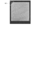
- FIG. 3 shows an EMS image of the photoelectric conversion element according to the first comparative example.
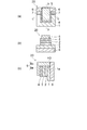
- FIGS. 4A to 4C are schematic views showing a photoelectric conversion element according to the first comparative example.
- FIG. 5 is a graph illustrating a second example of the photoelectric conversion element according to the embodiment.
- FIG. 6A and FIG. 6B are a table and a graph illustrating a third example of the photoelectric conversion element according to the embodiment.
- FIG. 7A and FIG. 7B are a table and a graph illustrating a third example of the photoelectric conversion element according to the embodiment.
- FIG. 1 is a schematic diagram illustrating a photoelectric conversion element according to an embodiment.
- FIG. 1A is a schematic plan view illustrating a photoelectric conversion element according to an embodiment.
- FIG. 1B is a schematic cross-sectional view taken along the section AA shown in FIG.
- FIG. 1C is a schematic cross-sectional view taken along the line BB shown in FIG.
- FIG.1 (d) is the typical enlarged view to which area
- the photoelectric conversion element 10 includes a first electrode 1, a first buffer layer 2, a photoelectric conversion layer 3, a second buffer layer 4, a second electrode 5, a substrate 6, A third buffer layer 7.
- Examples of the photoelectric conversion element 10 according to the embodiment include a solar cell and a sensor.
- the photoelectric conversion layer 3 is formed by coating and includes at least one of an organic semiconductor material and a perovskite structure material.
- the second electrode 5 is provided separately from the first electrode 1.
- the first electrode 1 is provided between the substrate 6 and the second electrode 5.
- the first buffer layer 2 is provided between the first electrode 1 and the second electrode 5.
- the photoelectric conversion layer 3 is provided between the first buffer layer 2 and the second electrode 5.
- the second buffer layer 4 is provided between the photoelectric conversion layer 3 and the second electrode 5.
- the third buffer layer 7 is provided at the end 1 a of the first electrode 1. More specifically, as shown in FIG. 1D, the second electrode 5 includes a first portion 5a and a second portion 5b. The first portion 5 a is provided on the second buffer layer 4. The second portion 5 b extends from the first portion 5 a to the first electrode 1.
- the third buffer layer has a first buffer portion 7a and a second buffer portion 7b.
- the first electrode 1, the first buffer layer 2, the photoelectric conversion layer 3, and the second buffer layer 4 are provided between the substrate 6 and the first portion 5 a of the second electrode 5.
- the first buffer portion 7 a of the third buffer layer 7 is provided between the first electrode 1 and the first portion 5 a of the second electrode 5.
- the second buffer portion 7 b of the third buffer layer 7 is provided between the first electrode 1 and the second portion 5 b of the second electrode 5.
- One of the first electrode 1 and the second electrode 5 serves as an anode.
- One of the first electrode 1 and the second electrode 5 serves as a cathode. Electricity is taken out by the first electrode 1 and the second electrode 5.
- the photoelectric conversion layer 3 is excited by light incident through the substrate 6, the first electrode 1 and the first buffer layer 2, or light incident through the second electrode 5 and the second buffer layer 4. Electrons are generated in one of the first electrode 1 and the second electrode 5, and holes are generated in the other of the first electrode 1 and the second electrode 5.
- the substrate 6 supports other components (components other than the substrate 6).
- the substrate 6 can form an electrode.
- the substrate 6 is preferably one that is not altered by heat or an organic solvent.
- the material of the substrate 6 include inorganic materials, plastics, polymer films, and metal substrates.
- the inorganic material include alkali-free glass and quartz glass.
- the plastic and polymer film materials include polyethylene, polyethylene terephthalate (PET), polyethylene naphthalate (PEN), polyimide, polyamide, polyamideimide, liquid crystal polymer, cycloolefin polymer, and the like.
- the material for the metal substrate include stainless steel (SUS) and silicon.
- a transparent one is used. That is, when the substrate 6 is disposed on the light incident side, a material having optical transparency is used as the material of the substrate 6.
- the electrode opposite to the substrate 6 is transparent or translucent, an opaque substrate may be used as the substrate 6. If the board
- a moth-eye structure antireflection film is provided on the light incident surface, so that the light can be efficiently captured and the energy conversion efficiency of the cell can be improved.
- the moth-eye structure has a regular protrusion arrangement on the surface of the order of 100 nanometers (nm).
- the refractive index in the thickness direction changes continuously due to the projection structure of the moth-eye structure. Therefore, the discontinuous change surface of the refractive index can be reduced by interposing the non-reflective film. This reduces light reflection and improves cell efficiency.
- First electrode 1 and second electrode 5 In the description of the first electrode 1 and the second electrode 5, when the term “electrode” is simply used, it means at least one of the first electrode 1 and the second electrode 5.
- the first electrode 1 and the second electrode 5 are not particularly limited as long as they have conductivity.
- a transparent or translucent conductive material is used as the material of the electrode on the light transmitting side (for example, the first electrode 1).
- the first electrode 1 and the second electrode 5 are formed by vacuum deposition, sputtering, ion plating, plating, coating, or the like.
- the material of the transparent or translucent electrode include conductive metal oxides and translucent metals.
- conductive glass, gold, platinum, silver, copper, or the like is used as the material for the transparent or translucent electrode.
- the material for the conductive glass examples include indium oxide, zinc oxide, tin oxide, and indium tin oxide (ITO), fluorine-doped tin oxide (FTO), indium zinc oxide and the like that are composites thereof.
- the electrode is manufactured as a film (NESA or the like) or a layer containing conductive glass.
- ITO or FTO is preferable as the electrode material.
- the electrode material may be an organic conductive polymer such as polyaniline and derivatives thereof, polythiophene and derivatives thereof, and the like.
- the thickness of the electrode is preferably 30 nm or more and 300 nm or less. If the thickness of the electrode is less than 30 nm, the conductivity is lowered and the resistance is increased. The decrease in conductivity is one of the causes of a decrease in photoelectric conversion efficiency. When the thickness of the electrode is thicker than 300 nm, the flexibility of ITO is lowered. When the flexibility of ITO decreases, the ITO may crack when stress is applied.
- the sheet resistance of the electrode is preferably as low as possible, and is preferably 10 ⁇ / ⁇ or less.
- the electrode may be a single layer or may have a structure in which layers containing materials having different work functions are stacked.
- the electrode When the electrode is formed in contact with the electron transport layer, it is preferable to use a material having a low work function as the electrode material.
- the material having a low work function include alkali metals and alkaline earth metals.
- examples of the material having a low work function include Li, In, Al, Ca, Mg, Sm, Tb, Yb, Zr, Na, K, Rb, Cs, Ba, and alloys thereof.
- the electrode may be a single layer or may have a structure in which layers containing materials having different work functions are stacked.
- the electrode material is an alloy of at least one of the above-described low work function materials and at least one of gold, silver, platinum, copper, manganese, titanium, cobalt, nickel, tungsten, and tin. But you can.
- the alloy include a lithium-aluminum alloy, a lithium-magnesium alloy, a lithium-indium alloy, a magnesium-silver alloy, a calcium-indium alloy, a magnesium-aluminum alloy, an indium-silver alloy, and a calcium-aluminum alloy.
- the thickness of the electrode is preferably 1 nm or more and 500 nm or less.
- the thickness of the electrode is more preferably 10 nm or more and 300 nm or less.
- the thickness of the electrode is less than 1 nm, the resistance increases compared to the case where the thickness of the electrode is 1 nm or more, and the generated charge may not be sufficiently transmitted to the external circuit.
- the thickness of the electrode is greater than 500 nm, it takes a relatively long time to form the electrode. Therefore, the material temperature rises, and the performance may be deteriorated by damaging other materials. Furthermore, since a large amount of material is used, the occupation time of an electrode forming apparatus (for example, a film forming apparatus) becomes longer, leading to an increase in cost.
- the electrode When the electrode is formed in contact with the hole transport layer, it is preferable to use a material having a high work function as the electrode material.
- the material having a high work function include Au, Ag, Cu, and alloys thereof.
- the electrode may be a single layer or may have a structure in which layers containing materials having different work functions are stacked.
- the thickness of the electrode is preferably 1 nm or more and 500 nm or less.
- the thickness of the electrode is more preferably 10 nm or more and 300 nm or less.
- the thickness of the electrode is less than 1 nm, the resistance increases compared to the case where the thickness of the electrode is 1 nm or more, and the generated charge may not be sufficiently transmitted to the external circuit.
- the thickness of the electrode is greater than 500 nm, it takes a relatively long time to form the electrode. Therefore, the material temperature rises, and the performance may be deteriorated by damaging other materials. Furthermore, since a large amount of material is used, the occupation time of an electrode forming apparatus (for example, a film forming apparatus) becomes longer, leading to an increase in cost.
- First buffer layer 2, second buffer layer 4, third buffer layer 7) One of the first buffer layer 2 and the second buffer layer 4 is provided between the photoelectric conversion layer 3 and the first electrode 1. The other of the first buffer layer 2 and the second buffer layer 4 is provided between the photoelectric conversion layer 3 and the second electrode 5.
- the first buffer layer 2 is provided between the photoelectric conversion layer 3 and the first electrode 1.
- the second buffer layer 4 is provided between the photoelectric conversion layer 3 and the second electrode 5.
- One of the first buffer layer 2 and the second buffer layer 4 is a hole transport layer.
- the other of the first buffer layer 2 and the second buffer layer 4 is an electron transport layer.
- the material of the second buffer layer 4 and the material of the third buffer layer 7 are preferably halogen compounds or metal oxides.
- the material of the second buffer layer 4 is preferably the same as the material of the third buffer layer 7. As shown in FIG. 1D, the thickness D 1 of the first buffer portion 7 a of the third buffer layer 7 is preferably thicker than the thickness D 2 of the second buffer layer 4.
- halogen compound examples include LiF, LiCl, LiBr, LiI, NaF, NaCl, NaBr, NaI, KF, KCl, KBr, KI, and CsF.
- a more preferred example of the halogen compound is LiF.
- the metal oxide include titanium oxide, molybdenum oxide, vanadium oxide, zinc oxide, nickel oxide, lithium oxide, calcium oxide, cesium oxide, and aluminum oxide.
- polythiophene polymers such as PEDOT: PSS (poly (3,4-ethylenedioxythiophene) -poly (styrenesulfonate)), and organic conductive polymers such as polyaniline and polypyrrole should be used.
- PEDOT polythiophene polymers
- PSS poly (3,4-ethylenedioxythiophene) -poly (styrenesulfonate)
- organic conductive polymers such as polyaniline and polypyrrole
- Clevios PH500, CleviosPH, CleviosPV P Al 4083, and CleviosHIL1, 1 from Starck are listed.
- An example of the inorganic material is molybdenum oxide.
- the thickness of the hole transport layer is preferably 20 nm or more and 100 nm or less.
- the thickness of the hole transport layer is thinner than 20 nm, the effect of preventing the lower electrode (first electrode 1 in the embodiment) from being short-circuited is reduced, and a short circuit occurs.
- the thickness of the hole transport layer is greater than 100 nm, the resistance becomes larger than that when the thickness of the hole transport layer is 100 nm or less, and the generated current is limited. Therefore, the light conversion efficiency is lowered.
- the formation method of a positive hole transport layer will not be specifically limited if it is a method which can form a thin film.
- the material for the hole transport layer can be applied by spin coating or the like. After the hole transport layer material is applied to a desired thickness, it is heated and dried with a hot plate or the like. It is preferable to heat and dry the applied hole transport layer material at 140 ° C. or higher and 200 ° C. or lower for several minutes or more and 10 minutes or less. As the solution to be applied, it is desirable to use a solution that has been filtered in advance.
- the electron transport layer has a function of efficiently transporting electrons.
- a metal oxide is mentioned as a material of an electron carrying layer. Examples of the metal oxide include amorphous titanium oxide obtained by hydrolyzing titanium alkoxide by a sol-gel method.
- the method for forming the electron transport layer is not particularly limited as long as it can form a thin film.
- a spin coating method can be given.
- the thickness of the electron transport layer is preferably 5 nm or more and 20 nm or less.
- the hole blocking effect is reduced. Therefore, the generated excitons are deactivated before dissociating into electrons and holes, and current cannot be extracted efficiently.
- the thickness of the electron transport layer is greater than 20 nm, the resistance of the electron transport layer is increased and the generated current is limited as compared with the case where the thickness of the electron transport layer is 20 nm or less. Therefore, the light conversion efficiency is lowered.
- the electron transport layer material After applying the electron transport layer material to the specified thickness, heat and dry using a hot plate.
- the material of the applied electron transport layer is heated and dried at 50 ° C. or more and 100 ° C. or less for several minutes or more and 10 minutes or less while promoting hydrolysis in the air.
- the inorganic material include metallic calcium.
- a heterojunction or a bulk heterojunction made of an organic semiconductor can be used.
- a p-type semiconductor and an n-type semiconductor are mixed in the photoelectric conversion layer 3 to form a micro layer separation structure. This is generally called a bulk heterojunction.
- the mixed p-type semiconductor and n-type semiconductor form a pn junction having a nano-order size in the photoelectric conversion layer 3, and obtain an electric current by utilizing photoelectric charge separation generated at the junction surface.
- the p-type semiconductor includes a material having an electron donating property.
- the n-type semiconductor includes a material having an electron-accepting property.
- at least one of the p-type semiconductor and the n-type semiconductor may be an organic semiconductor.
- Examples of p-type organic semiconductors include polythiophene and derivatives thereof, polypyrrole and derivatives thereof, pyrazoline derivatives, arylamine derivatives, stilbene derivatives, triphenyldiamine derivatives, oligothiophene and derivatives thereof, polyvinylcarbazole and derivatives thereof, polysilane and derivatives thereof.
- Polysiloxane derivatives having aromatic amines in the side chain or main chain, polyaniline and derivatives thereof, phthalocyanine derivatives, porphyrins and derivatives thereof, polyphenylene vinylene and derivatives thereof, polythienylene vinylene and derivatives thereof, and the like can be used, These may be used in combination. Moreover, you may use these copolymers.
- Examples of the copolymer include a thiophene-fluorene copolymer, a phenylene ethynylene-phenylene vinylene copolymer, and the like.
- polythiophene which is a conductive polymer having ⁇ conjugation and derivatives thereof are preferable.
- Polythiophene and its derivatives can ensure relatively good stereoregularity.
- the solubility of polythiophene and its derivatives in the solvent is relatively high.
- Polythiophene and derivatives thereof are not particularly limited as long as they are compounds having a thiophene skeleton. Specific examples of polythiophene and derivatives thereof include polyalkylthiophene; poly-3-phenylthiophene, polyarylthiophene; poly-3-butylisothionaphthene, polyalkylisothionaphthene; polyethylenedioxythiophene and the like.
- Polyalkylthiophene examples include poly-3-methylthiophene, poly-3-butylthiophene, poly-3-hexylthiophene, poly-3-octylthiophene, poly-3-decylthiophene, poly-3-dodecylthiophene, etc. It is done.
- Polyarylthiophene; Examples of poly-3-butylisothionaphthene include poly-3- (p-alkylphenylthiophene).
- Polyalkylisothionaphthene examples include poly-3-hexylisothionaphthene, poly-3-octylisothionaphthene, poly-3-decylisothionaphthene, and the like.
- PCDTBT poly [N-9 "-hepta-decanyl-2,7-carbazole-alt-5,5- (4 ', 7'-di-2), which is a copolymer containing carbazole, benzothiadiazole and thiophene, is also used.
- Derivatives such as -thienyl-2 ′, 1 ′, 3′-benzothiadiazole)]) are known as compounds that can obtain relatively excellent photoelectric conversion efficiency.
- These conductive polymers can be formed as a film or a layer by applying a solution dissolved in a solvent. Therefore, a large-area organic thin film solar cell can be manufactured at low cost with inexpensive equipment by a printing method or the like.
- fullerene and derivatives thereof are preferable.
- the fullerene derivative used here is not particularly limited as long as it is a derivative having a fullerene skeleton. Specific examples include derivatives composed of C 60 , C 70 , C 76 , C 78 , C 84 and the like as a basic skeleton.
- carbon atoms in the fullerene skeleton may be modified with an arbitrary functional group, and these functional groups may be bonded to each other to form a ring.
- Fullerene derivatives include fullerene bonded polymers. A fullerene derivative having a functional group with high affinity for the solvent and high solubility in the solvent is preferred.
- Examples of the functional group in the fullerene derivative include a hydrogen atom; a hydroxyl group; a fluorine atom, a halogen atom; a methyl group, an alkyl group; an alkenyl group; a cyano group; a methoxy group, an alkoxy group; a phenyl group, an aromatic hydrocarbon group, and a thienyl group. And aromatic heterocyclic groups.
- Examples of the halogen atom include a chlorine atom.
- Examples of the alkyl group include an ethyl group.
- Examples of the alkenyl group include a vinyl group.
- Examples of the alkoxy group include an ethoxy group.
- Examples of the aromatic hydrocarbon group include a naphthyl group.
- aromatic heterocyclic group examples include a pyridyl group.
- specific examples include hydrogenated fullerenes such as C 60 H 36 and C 70 H 36 , oxide fullerenes such as C 60 and C 70 , fullerene metal complexes, and the like.
- 60PCBM [6,6] -phenyl C 61 butyric acid methyl ester
- 70PCBM [6,6] -phenyl C 71 butyric acid methyl ester
- the unmodified fullerene when using the unmodified fullerene as n-type organic semiconductor, it is preferred to use a C 70. Generation efficiency of photocarriers of the fullerene C 70 is relatively high. It is preferable to use a fullerene C 70 in the organic thin film solar cell.
- the solvent used therefor include unsaturated hydrocarbon solvents, halogenated aromatic hydrocarbon solvents, halogenated saturated hydrocarbon solvents, ethers, and the like.
- unsaturated hydrocarbon solvent include toluene, xylene, tetralin, decalin, mesitylene, n-butylbenzene, sec-butylbenzene, tert-butylbenzene and the like.
- halogenated aromatic hydrocarbon solvent include chlorobenzene, dichlorobenzene, and trichlorobenzene.
- halogenated saturated hydrocarbon solvent examples include carbon tetrachloride, chloroform, dichloromethane, dichloroethane, chlorobutane, bromobutane, chloropentane, chlorohexane, bromohexane, and chlorocyclohexane.
- ethers include tetrahydrofuran and tetrahydropyran.
- a halogen-based aromatic solvent is more preferable. These solvents can be used alone or in combination.
- Examples of methods for forming a film or layer by applying a solution include spin coating, dip coating, casting, bar coating, roll coating, wire bar coating, spraying, screen printing, gravure printing, flexographic printing. Method, offset printing method, gravure offset printing, dispenser coating, nozzle coating method, capillary coating method, ink jet method and the like. These coating methods can be used alone or in combination.
- Perovskite can be used for the photoelectric conversion layer 3.
- Perovskite can be represented by ABX 3 composed of ions A, ions B, and ions X.
- ABX 3 may have a perovskite structure.
- the perovskite structure has a cubic unit cell. In the perovskite structure, an ion A is arranged at each vertex of a cubic crystal, an ion B is arranged at the body center, and an ion X is arranged at each face center of the cubic crystal around this.
- the orientation of the BX 6 octahedron is easily distorted by the interaction with the ions A.
- the BX 6 octahedron undergoes a Mott transition due to a decrease in symmetry.
- the valence electrons localized in the ions M can spread as a band.
- the ion A is preferably CH 3 NH 3 .
- the ion B is preferably at least one of Pb and Sn.
- the ion X is preferably at least one of Cl, Br, and I.
- the materials constituting the ions A, ions B, and ions X may be single or mixed.
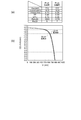
- FIG. 2 is a table and a graph illustrating a first example of the photoelectric conversion element according to the embodiment.
- FIG. 3 shows an EMS (Emission Microscopy) image of the photoelectric conversion element according to the first comparative example.
- FIG. 4 is a schematic diagram illustrating a photoelectric conversion element according to a first comparative example.
- FIG. 2 (a) is a table showing the characteristics of the first example and the first comparative example.
- FIG. 2B is a graph illustrating the relationship between voltage and current density. The horizontal axis of the graph shown in FIG. The vertical axis of the graph shown in FIG. 2B represents the current density CD.
- FIG. 4A is a schematic plan view showing the photoelectric conversion element according to the embodiment.
- FIG. 4B is a schematic cross-sectional view taken along a section CC shown in FIG.
- FIG. 4C is a schematic cross-sectional view taken along the section line DD shown in FIG.
- a glass plate is used for the substrate 6 and ITO is used for the first electrode 1.
- PEDOT: PSS is formed as the first buffer layer 2 and LiF is formed as the second buffer layer 4.
- the first buffer layer 2 functions as a hole transport layer.
- the second buffer layer 4 functions as an electron transport layer.
- PTB7 is formed as a p-type organic semiconductor material of the photoelectric conversion layer 3, and [70] PCBM bulk hetero is formed as an n-type organic semiconductor material.
- the solution is CB containing 3% DIO.
- 0.02 nm of LiF is formed by a vapor deposition machine, and as the second electrode 5, 100 nm of AgMg (Mg: 90 wt%) is formed.
- the film thickness of LiF formed here (indicated value of the film thickness meter of the vapor deposition machine) is smaller than the diameter of Li atom 0.34 nm. It is difficult to think of a continuous film, meaning an average film thickness.
- the photoelectric conversion element 20 according to the first comparative example does not have the third buffer layer 7.
- the first buffer layer 2 extends to the end 1 a of the first electrode 1.
- Other structures are the same as those of the photoelectric conversion element 10 according to the first embodiment.
- the conversion efficiency ( ⁇ (%)) of the photoelectric conversion element 20 according to the first comparative example is compared with the conversion efficiency of the photoelectric conversion element 10 according to the first example. It turns out that it is falling.
- region A2 shown in FIG. 3 it can be seen that current leaks at the end 1a of the photoelectric conversion element 20 according to the first comparative example.
- a region A2 illustrated in FIG. 3 corresponds to a region A3 (the end 1a of the first electrode 1) illustrated in FIG.
- the third buffer layer 7 has the end 1a of the first electrode 1 (a portion corresponding to the region A3 shown in FIG. 4C). Is provided. As a result, a decrease in shunt resistance can be suppressed, and current leakage can be suppressed.
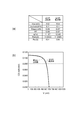
- FIG. 5 is a graph illustrating a second example of the photoelectric conversion element according to the embodiment.
- the structure of the photoelectric conversion element 10 according to the second embodiment is as described above with reference to FIGS. 1 (a) to 1 (b).
- the shape of the photoelectric conversion layer 3 when viewed in the direction of FIG. 1A, the shape of the photoelectric conversion layer 3 is 4.4 millimeters (mm) ⁇ 23 mm, and the first electrode 1 (ITO ) Is set to 4.4 mm. That is, in the photoelectric conversion element 10 according to the first example, the shape of the photoelectric conversion layer 3 and the shape of the first electrode 1 are not square but rectangular (except for a square). Based on the shape of the photoelectric conversion layer 3 and the first electrode 1, the photoelectric conversion element 10 according to the second example having the same configuration as the photoelectric conversion element 10 according to the first example is manufactured.
- the photoelectric conversion element according to the second comparative example has the same structure as the photoelectric conversion element 20 according to the first comparative example. That is, the structure of the photoelectric conversion element according to the second comparative example is as described above with reference to FIGS. 4 (a) to 4 (c).
- the photoelectric conversion layer 3 of the second comparative example has a rectangular shape (excluding a square).
- the first electrode 1 of the second comparative example has a rectangular shape (excluding a square).
- FIG. 5 an example of a result of measuring characteristics generated by incident light of 100 mW / cm 2 at AM 1.5 is shown in FIG. As shown. As shown in FIG. 5, it can be seen that the conversion efficiency of the photoelectric conversion element 10 according to the second example is higher than the conversion efficiency of the photoelectric conversion element according to the second comparative example.
- the photoelectric conversion element 10 according to the second example can suppress the decrease in the shunt resistance and suppress the leakage of the current.
- FIGS. 6 and 7 are a table and a graph for explaining a third example of the photoelectric conversion element according to the embodiment.
- FIG. 6A and FIG. 7A are tables showing the characteristics of the third example and the third comparative example.
- FIG. 6B and FIG. 7B are graphs illustrating the relationship between voltage and current density.
- the horizontal axis of the graphs shown in FIGS. 6B and 7B represents the voltage V.
- the vertical axis of the graphs shown in FIGS. 6B and 7B represents the current density CD.
- the structure of the photoelectric conversion element 10 according to the third embodiment is as described above with reference to FIGS. 1 (a) to 1 (b).
- the first buffer layer 2 is made of ZnO
- the second buffer layer 4 and the third buffer layer 7 are made of V 2 O 5
- the second electrode 5 is made of Ag.
- the first buffer layer 2 functions as an electron transport layer.
- the second buffer layer 4 functions as a hole transport layer.
- the first buffer layer 2 functions as a hole transport layer
- the second buffer layer 4 functions as an electron transport layer.
- the photoelectric conversion element according to the third comparative example has the same structure as the photoelectric conversion element 20 according to the first comparative example. That is, the structure of the photoelectric conversion element according to the third comparative example is as described above with reference to FIGS. 4 (a) to 4 (c).
- the first buffer layer 2 is made of ZnO
- the second buffer layer 4 is made of V 2 O 5
- the second electrode 5 is made of Ag.
- FIG. 10 In the photoelectric conversion element 10 according to the third example and the photoelectric conversion element according to the third comparative example, electrons are extracted from the first electrode 1 and holes are extracted from the second electrode 5.
- FIG. 10 An example of a result of measuring characteristics generated by incident light of 100 mW / cm 2 at AM 1.5 is shown in FIG. It is as having represented to a) and FIG.6 (b).
- FIGS. 7 (a) and 7 (b) an example of the result of measuring the characteristics generated by incident light of indoor light (LED) of 1000 lux (Lux) is as shown in FIGS. 7 (a) and 7 (b).
- the conversion efficiency of the photoelectric conversion element 10 according to the third example is compared with the conversion efficiency of the photoelectric conversion element according to the third comparative example. You can see that it is rising. Thereby, even if the 1st buffer layer 2 is any of a positive hole transport layer and an electron carrying layer, the photoelectric conversion element 10 concerning embodiment can suppress the fall of shunt resistance, and an electric current leaks. That can be suppressed. Moreover, even if the 2nd buffer layer 4 is any of a positive hole transport layer and an electron carrying layer, the photoelectric conversion element 10 concerning embodiment can suppress the fall of shunt resistance, and an electric current leaks. Can be suppressed. According to the embodiment, a photoelectric conversion element that can suppress a decrease in shunt resistance can be provided.
- a photoelectric conversion element capable of suppressing a decrease in shunt resistance.
Landscapes
- Physics & Mathematics (AREA)
- Electromagnetism (AREA)
- Engineering & Computer Science (AREA)
- Power Engineering (AREA)
- Chemical & Material Sciences (AREA)
- Chemical Kinetics & Catalysis (AREA)
- Electrochemistry (AREA)
- Microelectronics & Electronic Packaging (AREA)
- Photovoltaic Devices (AREA)
- Light Receiving Elements (AREA)
Abstract
One embodiment of the present invention provides a photoelectric conversion element which is provided with a first electrode, a second electrode, a photoelectric conversion layer, a first buffer layer, a second buffer layer and a third buffer layer. The second electrode is arranged so as to be separated from the first electrode. The photoelectric conversion layer is arranged between the first electrode and the second electrode. The first buffer layer is arranged between the first electrode and the photoelectric conversion layer. The second buffer layer is arranged between the second electrode and the photoelectric conversion layer. The third buffer layer is arranged on an end portion of the first electrode.
Description
本発明の実施形態は、光電変換素子に関する。
Embodiments of the present invention relate to a photoelectric conversion element.
有機光電変換材料または有機物と無機物とを含む光電変換材料を用いた太陽電池やセンサーなどが研究開発されている。光電変換材料を塗布あるいは印刷することにより太陽電池等を生産できると、比較的低コストでデバイスを作製できる可能性がある。
塗布により光電変換層を形成する場合、光電変換材料を含むインクを電極上に塗布すると、下地電極の端部に形成される光電変換層の厚さは、端部以外の部分の光電変換層の厚さに比べて、インクの流動により薄くなる。電極の端部は、電界が集中する部分である。そのため、光電変換層の厚さが比較的薄いと、シャント抵抗が低下し、デバイス特性を低下させることがある。光電変換素子において、シャント抵抗の低下を抑制することが望まれる。 Research and development have been conducted on solar cells and sensors using organic photoelectric conversion materials or photoelectric conversion materials containing organic and inorganic substances. If a solar cell or the like can be produced by applying or printing a photoelectric conversion material, there is a possibility that a device can be manufactured at a relatively low cost.
When the photoelectric conversion layer is formed by coating, when the ink containing the photoelectric conversion material is applied on the electrode, the thickness of the photoelectric conversion layer formed on the end portion of the base electrode is equal to that of the photoelectric conversion layer in the portion other than the end portion. Compared to the thickness, it becomes thinner due to the flow of ink. The end portion of the electrode is a portion where the electric field concentrates. Therefore, when the thickness of the photoelectric conversion layer is relatively thin, the shunt resistance is lowered, and device characteristics may be lowered. In a photoelectric conversion element, it is desired to suppress a decrease in shunt resistance.
本発明の実施形態は、シャント抵抗の低下を抑制することができる光電変換素子を提供する。
Embodiment of this invention provides the photoelectric conversion element which can suppress the fall of shunt resistance.
実施形態によれば、第1の電極と、第2の電極と、光電変換層と、第1のバッファ層と、第2のバッファ層と、第3のバッファ層と、を備えた光電変換素子が提供される。前記第2の電極は、前記第1の電極と離隔して設けられる。前記光電変換層は、前記第1の電極と前記第2の電極との間に設けられる。前記第1のバッファ層は、前記第1の電極と前記光電変換層との間に設けられる。前記第2のバッファ層は、前記第2の電極と前記光電変換層との間に設けられる。前記第3のバッファ層は、前記第1の電極の端部に設けられる。
According to the embodiment, the photoelectric conversion element including the first electrode, the second electrode, the photoelectric conversion layer, the first buffer layer, the second buffer layer, and the third buffer layer. Is provided. The second electrode is provided apart from the first electrode. The photoelectric conversion layer is provided between the first electrode and the second electrode. The first buffer layer is provided between the first electrode and the photoelectric conversion layer. The second buffer layer is provided between the second electrode and the photoelectric conversion layer. The third buffer layer is provided at an end of the first electrode.
以下に、本発明の各実施の形態について図面を参照しつつ説明する。
なお、図面は模式的または概念的なものであり、各部分の厚みと幅との関係、部分間の大きさの比率などは、必ずしも現実のものと同一とは限らない。また、同じ部分を表す場合であっても、図面により互いの寸法や比率が異なって表される場合もある。
なお、本願明細書と各図において、既出の図に関して前述したものと同様の要素には同一の符号を付して詳細な説明は適宜省略する。 Embodiments of the present invention will be described below with reference to the drawings.
The drawings are schematic or conceptual, and the relationship between the thickness and width of each part, the size ratio between the parts, and the like are not necessarily the same as actual ones. Further, even when the same part is represented, the dimensions and ratios may be represented differently depending on the drawings.
Note that, in the present specification and each drawing, the same elements as those described above with reference to the previous drawings are denoted by the same reference numerals, and detailed description thereof is omitted as appropriate.
図1は、実施形態にかかる光電変換素子を表す模式図である。
図1(a)は、実施形態にかかる光電変換素子を表す模式的平面図である。図1(b)は、図1(a)に表した切断面A-Aにおける模式的断面図である。図1(c)は、図1(a)に表した切断面B-Bにおける模式的断面図である。図1(d)は、図1(c)に表した領域A1を拡大した模式的拡大図である。 FIG. 1 is a schematic diagram illustrating a photoelectric conversion element according to an embodiment.
FIG. 1A is a schematic plan view illustrating a photoelectric conversion element according to an embodiment. FIG. 1B is a schematic cross-sectional view taken along the section AA shown in FIG. FIG. 1C is a schematic cross-sectional view taken along the line BB shown in FIG. FIG.1 (d) is the typical enlarged view to which area | region A1 represented to FIG.1 (c) was expanded.
実施形態にかかる光電変換素子10は、第1の電極1と、第1のバッファ層2と、光電変換層3と、第2のバッファ層4と、第2の電極5と、基板6と、第3のバッファ層7と、を備える。実施形態にかかる光電変換素子10としては、例えば、太陽電池やセンサなどが挙げられる。光電変換層3は、塗布で形成され、有機半導体の材料およびペロブスカイト構造の材料の少なくともいずれかを含む。
The photoelectric conversion element 10 according to the embodiment includes a first electrode 1, a first buffer layer 2, a photoelectric conversion layer 3, a second buffer layer 4, a second electrode 5, a substrate 6, A third buffer layer 7. Examples of the photoelectric conversion element 10 according to the embodiment include a solar cell and a sensor. The photoelectric conversion layer 3 is formed by coating and includes at least one of an organic semiconductor material and a perovskite structure material.
図1(b)に表したように、第2の電極5は、第1の電極1と離隔して設けられる。第1の電極1は、基板6と、第2の電極5と、の間に設けられる。第1のバッファ層2は、第1の電極1と、第2の電極5と、の間に設けられる。光電変換層3は、第1のバッファ層2と、第2の電極5と、の間に設けられる。第2のバッファ層4は、光電変換層3と、第2の電極5と、の間に設けられる。
As shown in FIG. 1B, the second electrode 5 is provided separately from the first electrode 1. The first electrode 1 is provided between the substrate 6 and the second electrode 5. The first buffer layer 2 is provided between the first electrode 1 and the second electrode 5. The photoelectric conversion layer 3 is provided between the first buffer layer 2 and the second electrode 5. The second buffer layer 4 is provided between the photoelectric conversion layer 3 and the second electrode 5.
図1(a)および図1(c)に表したように、第3のバッファ層7は、第1の電極1の端部1aに設けられる。
より具体的には、図1(d)に表したように、第2の電極5は、第1の部分5aと、第2の部分5bと、を有する。第1の部分5aは、第2のバッファ層4の上に設けられる。第2の部分5bは、第1の部分5aから第1の電極1へ延在する。第3のバッファ層は、第1のバッファ部分7aと、第2のバッファ部分7bと、を有する。第1の電極1、第1のバッファ層2、光電変換層3、および第2のバッファ層4は、基板6と、第2の電極5の第1の部分5aと、の間に設けられる。第3のバッファ層7の第1のバッファ部分7aは、第1の電極1と、第2の電極5の第1の部分5aと、の間に設けられる。第3のバッファ層7の第2のバッファ部分7bは、第1の電極1と、第2の電極5の第2の部分5bと、の間に設けられる。 As shown in FIGS. 1A and 1C, thethird buffer layer 7 is provided at the end 1 a of the first electrode 1.
More specifically, as shown in FIG. 1D, thesecond electrode 5 includes a first portion 5a and a second portion 5b. The first portion 5 a is provided on the second buffer layer 4. The second portion 5 b extends from the first portion 5 a to the first electrode 1. The third buffer layer has a first buffer portion 7a and a second buffer portion 7b. The first electrode 1, the first buffer layer 2, the photoelectric conversion layer 3, and the second buffer layer 4 are provided between the substrate 6 and the first portion 5 a of the second electrode 5. The first buffer portion 7 a of the third buffer layer 7 is provided between the first electrode 1 and the first portion 5 a of the second electrode 5. The second buffer portion 7 b of the third buffer layer 7 is provided between the first electrode 1 and the second portion 5 b of the second electrode 5.
より具体的には、図1(d)に表したように、第2の電極5は、第1の部分5aと、第2の部分5bと、を有する。第1の部分5aは、第2のバッファ層4の上に設けられる。第2の部分5bは、第1の部分5aから第1の電極1へ延在する。第3のバッファ層は、第1のバッファ部分7aと、第2のバッファ部分7bと、を有する。第1の電極1、第1のバッファ層2、光電変換層3、および第2のバッファ層4は、基板6と、第2の電極5の第1の部分5aと、の間に設けられる。第3のバッファ層7の第1のバッファ部分7aは、第1の電極1と、第2の電極5の第1の部分5aと、の間に設けられる。第3のバッファ層7の第2のバッファ部分7bは、第1の電極1と、第2の電極5の第2の部分5bと、の間に設けられる。 As shown in FIGS. 1A and 1C, the
More specifically, as shown in FIG. 1D, the
第1の電極1および第2の電極5のいずれか一方は、陽極となる。第1の電極1および第2の電極5のいずれか他方は、陰極となる。第1の電極1および第2の電極5により、電気が取り出される。光電変換層3は、基板6と第1の電極1と第1のバッファ層2とを通して入射した光、または第2の電極5と第2のバッファ層4とを通して入射した光によって励起され、第1の電極1および第2の電極5のいずれか一方に電子を生じ、第1の電極1および第2の電極5のいずれか他方に正孔を生ずる。
以下、実施形態に係る光電変換素子10の構成部材について説明する。 One of thefirst electrode 1 and the second electrode 5 serves as an anode. One of the first electrode 1 and the second electrode 5 serves as a cathode. Electricity is taken out by the first electrode 1 and the second electrode 5. The photoelectric conversion layer 3 is excited by light incident through the substrate 6, the first electrode 1 and the first buffer layer 2, or light incident through the second electrode 5 and the second buffer layer 4. Electrons are generated in one of the first electrode 1 and the second electrode 5, and holes are generated in the other of the first electrode 1 and the second electrode 5.
Hereinafter, constituent members of thephotoelectric conversion element 10 according to the embodiment will be described.
以下、実施形態に係る光電変換素子10の構成部材について説明する。 One of the
Hereinafter, constituent members of the
(基板6)
基板6は、ほかの構成部材(基板6以外の構成部材)を支持する。基板6は、電極を形成することができる。基板6としては、熱や有機溶媒によって変質しないものが好ましい。基板6の材料としては、例えば、無機材料、プラスチック、高分子フィルム、あるいは金属基板等が挙げられる。無機材料としては、無アルカリガラス、石英ガラス等が挙げられる。プラスチックおよび高分子フィルムの材料としては、ポリエチレン、ポリエチレンテレフタレート(PET)、ポリエチレンナフタレート(PEN)、ポリイミド、ポリアミド、ポリアミドイミド、液晶ポリマー、シクロオレフィンポリマー等などが挙げられる。金属基板の材料としては、ステンレス鋼(SUS)、シリコン等が挙げられる。 (Substrate 6)
Thesubstrate 6 supports other components (components other than the substrate 6). The substrate 6 can form an electrode. The substrate 6 is preferably one that is not altered by heat or an organic solvent. Examples of the material of the substrate 6 include inorganic materials, plastics, polymer films, and metal substrates. Examples of the inorganic material include alkali-free glass and quartz glass. Examples of the plastic and polymer film materials include polyethylene, polyethylene terephthalate (PET), polyethylene naphthalate (PEN), polyimide, polyamide, polyamideimide, liquid crystal polymer, cycloolefin polymer, and the like. Examples of the material for the metal substrate include stainless steel (SUS) and silicon.
基板6は、ほかの構成部材(基板6以外の構成部材)を支持する。基板6は、電極を形成することができる。基板6としては、熱や有機溶媒によって変質しないものが好ましい。基板6の材料としては、例えば、無機材料、プラスチック、高分子フィルム、あるいは金属基板等が挙げられる。無機材料としては、無アルカリガラス、石英ガラス等が挙げられる。プラスチックおよび高分子フィルムの材料としては、ポリエチレン、ポリエチレンテレフタレート(PET)、ポリエチレンナフタレート(PEN)、ポリイミド、ポリアミド、ポリアミドイミド、液晶ポリマー、シクロオレフィンポリマー等などが挙げられる。金属基板の材料としては、ステンレス鋼(SUS)、シリコン等が挙げられる。 (Substrate 6)
The
基板6は、光が入射する側に配置される場合、透明なものを使用する。つまり、光が入射する側に基板6が配置される場合には、基板6の材料として、光透過性を有する材料が用いられる。基板6とは反対側の電極(実施形態では第2の電極5)が透明または半透明である場合、基板6として不透明な基板を使用してもよい。基板6が他の構成部材を支持するために十分な強度を有していれば、基板6の厚さは、特に限定されない。
When the substrate 6 is disposed on the light incident side, a transparent one is used. That is, when the substrate 6 is disposed on the light incident side, a material having optical transparency is used as the material of the substrate 6. When the electrode opposite to the substrate 6 (second electrode 5 in the embodiment) is transparent or translucent, an opaque substrate may be used as the substrate 6. If the board | substrate 6 has sufficient intensity | strength to support another structural member, the thickness of the board | substrate 6 will not be specifically limited.
基板6は、光が入射する側に配置される場合、例えばモスアイ構造の反射防止膜を光入射面に設置することで光を効率的に取り込み、セルのエネルギー変換効率を向上させることが可能である。モスアイ構造は、100ナノメートル(nm)程度の規則的な突起配列を表面に有する。モスアイ構造の突起構造により、厚み方向の屈折率が連続的に変化する。そのため、無反射フィルムを媒介させることで屈折率の不連続的な変化面を減少させることができる。これにより、光の反射が減少し、セル効率が向上する。
When the substrate 6 is disposed on the light incident side, for example, a moth-eye structure antireflection film is provided on the light incident surface, so that the light can be efficiently captured and the energy conversion efficiency of the cell can be improved. is there. The moth-eye structure has a regular protrusion arrangement on the surface of the order of 100 nanometers (nm). The refractive index in the thickness direction changes continuously due to the projection structure of the moth-eye structure. Therefore, the discontinuous change surface of the refractive index can be reduced by interposing the non-reflective film. This reduces light reflection and improves cell efficiency.
(第1の電極1および第2の電極5)
第1の電極1および第2の電極5に関する説明において、単に「電極」という場合には、第1の電極1および第2の電極5の少なくともいずれかをいうものとする。 (First electrode 1 and second electrode 5)
In the description of thefirst electrode 1 and the second electrode 5, when the term “electrode” is simply used, it means at least one of the first electrode 1 and the second electrode 5.
第1の電極1および第2の電極5に関する説明において、単に「電極」という場合には、第1の電極1および第2の電極5の少なくともいずれかをいうものとする。 (
In the description of the
第1の電極1および第2の電極5は、導電性を有するものであれば特に限定されない。光を透過させる側の電極(例えば第1の電極1)の材料としては、透明または半透明の導電性を有する材料が用いられる。第1の電極1および第2の電極5は、真空蒸着法、スパッタリング法、イオンプレーティング法、メッキ法、塗布法等で形成される。透明または半透明の電極の材料としては、導電性の金属酸化物、半透明の金属等が挙げられる。具体的には、透明または半透明の電極の材料としては、導電性ガラスや、金、白金、銀、銅等が用いられる。導電性ガラスの材料としては、酸化インジウム、酸化亜鉛、酸化スズ、およびそれらの複合体であるインジウム・スズ・オキサイド(ITO)、フッ素ドープ酸化スズ(FTO)、インジウム・亜鉛・オキサイド等が挙げられる。例えば、電極は、導電性ガラスを含む膜(NESA等)あるいは層として作製される。電極の材料としては、例えばITOまたはFTOが好ましい。電極の材料は、有機系の導電性ポリマーであるポリアニリンおよびその誘導体、ポリチオフェンおよびその誘導体等であってもよい。
The first electrode 1 and the second electrode 5 are not particularly limited as long as they have conductivity. As the material of the electrode on the light transmitting side (for example, the first electrode 1), a transparent or translucent conductive material is used. The first electrode 1 and the second electrode 5 are formed by vacuum deposition, sputtering, ion plating, plating, coating, or the like. Examples of the material of the transparent or translucent electrode include conductive metal oxides and translucent metals. Specifically, as the material for the transparent or translucent electrode, conductive glass, gold, platinum, silver, copper, or the like is used. Examples of the material for the conductive glass include indium oxide, zinc oxide, tin oxide, and indium tin oxide (ITO), fluorine-doped tin oxide (FTO), indium zinc oxide and the like that are composites thereof. . For example, the electrode is manufactured as a film (NESA or the like) or a layer containing conductive glass. For example, ITO or FTO is preferable as the electrode material. The electrode material may be an organic conductive polymer such as polyaniline and derivatives thereof, polythiophene and derivatives thereof, and the like.
電極の材料がITOの場合には、電極の厚さは、30nm以上、300nm以下であることが好ましい。電極の厚さを30nmよりも薄くすると、導電性が低下して抵抗が高くなる。導電性の低下は、光電変換効率の低下の原因のひとつとなる。電極の厚さを300nmよりも厚くすると、ITOの可撓性が低下する。ITOの可撓性が低下すると、応力が作用したときにITOが割れることがある。
When the electrode material is ITO, the thickness of the electrode is preferably 30 nm or more and 300 nm or less. If the thickness of the electrode is less than 30 nm, the conductivity is lowered and the resistance is increased. The decrease in conductivity is one of the causes of a decrease in photoelectric conversion efficiency. When the thickness of the electrode is thicker than 300 nm, the flexibility of ITO is lowered. When the flexibility of ITO decreases, the ITO may crack when stress is applied.
電極のシート抵抗は可能な限り低いことが好ましく、10Ω/□以下であることが好ましい。電極は、単層であってもよく、異なる仕事関数の材料を含む層が積層された構造を有していてもよい。
The sheet resistance of the electrode is preferably as low as possible, and is preferably 10Ω / □ or less. The electrode may be a single layer or may have a structure in which layers containing materials having different work functions are stacked.
電極を電子輸送層と接して形成する場合には、電極の材料として仕事関数の低い材料を用いることが好ましい。仕事関数の低い材料としては、例えば、アルカリ金属、アルカリ土類金属等が挙げられる。具体的には、仕事関数の低い材料としては、Li、In、Al、Ca、Mg、Sm、Tb、Yb、Zr、Na、K、Rb、Cs、Ba、およびこれらの合金を挙げることができる。電極は、単層であってもよく、異なる仕事関数の材料を含む層が積層された構造を有していてもよい。また、電極の材料は、前述した仕事関数の低い材料のうちの少なくともいずれかと、金、銀、白金、銅、マンガン、チタン、コバルト、ニッケル、タングステン、および錫のうちの少なくともいずれかと、の合金でもよい。合金の例としては、リチウム-アルミニウム合金、リチウム-マグネシウム合金、リチウム-インジウム合金、マグネシウム-銀合金、カルシウム-インジウム合金、マグネシウム-アルミニウム合金、インジウム-銀合金、カルシウム-アルミニウム合金等が挙げられる。
When the electrode is formed in contact with the electron transport layer, it is preferable to use a material having a low work function as the electrode material. Examples of the material having a low work function include alkali metals and alkaline earth metals. Specifically, examples of the material having a low work function include Li, In, Al, Ca, Mg, Sm, Tb, Yb, Zr, Na, K, Rb, Cs, Ba, and alloys thereof. . The electrode may be a single layer or may have a structure in which layers containing materials having different work functions are stacked. The electrode material is an alloy of at least one of the above-described low work function materials and at least one of gold, silver, platinum, copper, manganese, titanium, cobalt, nickel, tungsten, and tin. But you can. Examples of the alloy include a lithium-aluminum alloy, a lithium-magnesium alloy, a lithium-indium alloy, a magnesium-silver alloy, a calcium-indium alloy, a magnesium-aluminum alloy, an indium-silver alloy, and a calcium-aluminum alloy.
電極を電子輸送層と接して形成する場合には、電極の厚さは、1nm以上、500nm以下であることが好ましい。電極の厚さは、10nm以上、300nm以下であることがより好ましい。電極の厚さが1nmよりも薄い場合には、電極の厚さが1nm以上の場合と比較して、抵抗が大きくなり、発生した電荷を十分に外部回路へ伝達できないことがある。電極の厚さが500nmよりも厚い場合には、電極の形成に比較的長い時間を要する。そのため、材料温度が上昇し、他の材料にダメージを与えて性能が劣化することがある。さらに、材料を大量に使用するため、電極を形成する装置(例えば成膜装置)の占有時間が長くなり、コストアップに繋がる。
When the electrode is formed in contact with the electron transport layer, the thickness of the electrode is preferably 1 nm or more and 500 nm or less. The thickness of the electrode is more preferably 10 nm or more and 300 nm or less. When the thickness of the electrode is less than 1 nm, the resistance increases compared to the case where the thickness of the electrode is 1 nm or more, and the generated charge may not be sufficiently transmitted to the external circuit. When the thickness of the electrode is greater than 500 nm, it takes a relatively long time to form the electrode. Therefore, the material temperature rises, and the performance may be deteriorated by damaging other materials. Furthermore, since a large amount of material is used, the occupation time of an electrode forming apparatus (for example, a film forming apparatus) becomes longer, leading to an increase in cost.
電極を正孔輸送層と接して形成する場合には、電極の材料として仕事関数の高い材料を用いることが好ましい。仕事関数の高い材料としては、例えば、Au、Ag、Cuおよびこれらの合金等が挙げられる。電極は、単層であってもよく、異なる仕事関数の材料を含む層が積層された構造を有していてもよい。
When the electrode is formed in contact with the hole transport layer, it is preferable to use a material having a high work function as the electrode material. Examples of the material having a high work function include Au, Ag, Cu, and alloys thereof. The electrode may be a single layer or may have a structure in which layers containing materials having different work functions are stacked.
電極を正孔輸送層と接して形成する場合には、電極の厚さは、1nm以上、500nm以下であることが好ましい。電極の厚さは、10nm以上、300nm以下であることがより好ましい。電極の厚さが1nmよりも薄い場合には、電極の厚さが1nm以上の場合と比較して、抵抗が大きくなり、発生した電荷を十分に外部回路へ伝達できないことがある。電極の厚さが500nmよりも厚い場合には、電極の形成に比較的長い時間を要する。そのため、材料温度が上昇し、他の材料にダメージを与えて性能が劣化することがある。さらに、材料を大量に使用するため、電極を形成する装置(例えば成膜装置)の占有時間が長くなり、コストアップに繋がる。
When the electrode is formed in contact with the hole transport layer, the thickness of the electrode is preferably 1 nm or more and 500 nm or less. The thickness of the electrode is more preferably 10 nm or more and 300 nm or less. When the thickness of the electrode is less than 1 nm, the resistance increases compared to the case where the thickness of the electrode is 1 nm or more, and the generated charge may not be sufficiently transmitted to the external circuit. When the thickness of the electrode is greater than 500 nm, it takes a relatively long time to form the electrode. Therefore, the material temperature rises, and the performance may be deteriorated by damaging other materials. Furthermore, since a large amount of material is used, the occupation time of an electrode forming apparatus (for example, a film forming apparatus) becomes longer, leading to an increase in cost.
(第1のバッファ層2、第2のバッファ層4、第3のバッファ層7)
第1のバッファ層2および第2のバッファ層4のいずれか一方は、光電変換層3と第1の電極1との間に設けられる。第1のバッファ層2および第2のバッファ層4のいずれか他方は、光電変換層3と第2の電極5との間に設けられる。図1(a)~図1(d)に表した例では、第1のバッファ層2は、光電変換層3と第1の電極1との間に設けられる。図1(a)~図1(d)に表した例では、第2のバッファ層4は、光電変換層3と第2の電極5との間に設けられる。 (First buffer layer 2, second buffer layer 4, third buffer layer 7)
One of thefirst buffer layer 2 and the second buffer layer 4 is provided between the photoelectric conversion layer 3 and the first electrode 1. The other of the first buffer layer 2 and the second buffer layer 4 is provided between the photoelectric conversion layer 3 and the second electrode 5. In the example shown in FIGS. 1A to 1D, the first buffer layer 2 is provided between the photoelectric conversion layer 3 and the first electrode 1. In the example shown in FIGS. 1A to 1D, the second buffer layer 4 is provided between the photoelectric conversion layer 3 and the second electrode 5.
第1のバッファ層2および第2のバッファ層4のいずれか一方は、光電変換層3と第1の電極1との間に設けられる。第1のバッファ層2および第2のバッファ層4のいずれか他方は、光電変換層3と第2の電極5との間に設けられる。図1(a)~図1(d)に表した例では、第1のバッファ層2は、光電変換層3と第1の電極1との間に設けられる。図1(a)~図1(d)に表した例では、第2のバッファ層4は、光電変換層3と第2の電極5との間に設けられる。 (
One of the
第1のバッファ層2および第2のバッファ層4のいずれか一方は、正孔輸送層である。第1のバッファ層2および第2のバッファ層4のいずれか他方は、電子輸送層である。第2のバッファ層4の材料および第3のバッファ層7の材料としては、ハロゲン化合物または金属酸化物が好ましい。第2のバッファ層4の材料は、第3のバッファ層7の材料と同じであることが好ましい。図1(d)に表したように、第3のバッファ層7の第1のバッファ部分7aの厚さD1は、第2のバッファ層4の厚さD2よりも厚いことが好ましい。
One of the first buffer layer 2 and the second buffer layer 4 is a hole transport layer. The other of the first buffer layer 2 and the second buffer layer 4 is an electron transport layer. The material of the second buffer layer 4 and the material of the third buffer layer 7 are preferably halogen compounds or metal oxides. The material of the second buffer layer 4 is preferably the same as the material of the third buffer layer 7. As shown in FIG. 1D, the thickness D 1 of the first buffer portion 7 a of the third buffer layer 7 is preferably thicker than the thickness D 2 of the second buffer layer 4.
ハロゲン化合物の例としては、LiF、LiCl、LiBr、LiI、NaF、NaCl、NaBr、 NaI、KF、KCl、KBr、KI、CsFが挙げられる。ハロゲン化合物のより好ましい例としては、LiFが挙げられる。
金属酸化物の例としては、チタン酸化物、モリブデン酸化物、バナジウム酸化物、亜鉛酸化物、ニッケル酸化物、リチウム酸化物、カルシウム酸化物、セシウム酸化物、アルミニウム酸化物が挙げられる。 Examples of the halogen compound include LiF, LiCl, LiBr, LiI, NaF, NaCl, NaBr, NaI, KF, KCl, KBr, KI, and CsF. A more preferred example of the halogen compound is LiF.
Examples of the metal oxide include titanium oxide, molybdenum oxide, vanadium oxide, zinc oxide, nickel oxide, lithium oxide, calcium oxide, cesium oxide, and aluminum oxide.
正孔輸送層の材料としては、PEDOT:PSS(ポリ(3,4-エチレンジオキシチオフェン)-ポリ(スチレンスルホネート))等のポリチオフェン系ポリマー、ポリアニリン、ポリピロール等の有機導電性ポリマーを使用することができる。ポリチオフェン系ポリマーの代表的な製品としては、例えば、スタルク社のClevios PH500、CleviosPH、CleviosPV P Al 4083、CleviosHIL1,1が挙げられる。無機物の材料としては、酸化モリブデンが挙げられる。
As the material for the hole transport layer, polythiophene polymers such as PEDOT: PSS (poly (3,4-ethylenedioxythiophene) -poly (styrenesulfonate)), and organic conductive polymers such as polyaniline and polypyrrole should be used. Can do. As typical products of the polythiophene-based polymer, for example, Clevios PH500, CleviosPH, CleviosPV P Al 4083, and CleviosHIL1, 1 from Starck are listed. An example of the inorganic material is molybdenum oxide.
正孔輸送層の材料としてClevios PH500を使用する場合には、正孔輸送層の厚さは、20nm以上、100nm以下であることが好ましい。正孔輸送層の厚さが20nmよりも薄い場合には、下部電極(実施形態では第1の電極1)の短絡を防止する作用が低下し、ショートが発生する。正孔輸送層の厚さが100nmよりも厚い場合には、正孔輸送層の厚さが100nm以下の場合と比較して抵抗が大きくなり、発生した電流を制限する。そのため、光変換効率が低下する。正孔輸送層の形成方法は、薄膜を形成できる方法であれば特に限定されない。例えば、スピンコート等で正孔輸送層の材料を塗布することが可能である。正孔輸送層の材料を所望の厚さに塗布した後、ホットプレート等で加熱し乾燥させる。140℃以上、200℃以下で数分間以上、10分間以下程度、塗布した正孔輸送層の材料を加熱し乾燥させることが好ましい。塗布する溶液は、予めフィルターでろ過したものを使用することが望ましい。
When Clevios PH500 is used as the material for the hole transport layer, the thickness of the hole transport layer is preferably 20 nm or more and 100 nm or less. When the thickness of the hole transport layer is thinner than 20 nm, the effect of preventing the lower electrode (first electrode 1 in the embodiment) from being short-circuited is reduced, and a short circuit occurs. When the thickness of the hole transport layer is greater than 100 nm, the resistance becomes larger than that when the thickness of the hole transport layer is 100 nm or less, and the generated current is limited. Therefore, the light conversion efficiency is lowered. The formation method of a positive hole transport layer will not be specifically limited if it is a method which can form a thin film. For example, the material for the hole transport layer can be applied by spin coating or the like. After the hole transport layer material is applied to a desired thickness, it is heated and dried with a hot plate or the like. It is preferable to heat and dry the applied hole transport layer material at 140 ° C. or higher and 200 ° C. or lower for several minutes or more and 10 minutes or less. As the solution to be applied, it is desirable to use a solution that has been filtered in advance.
電子輸送層は、電子を効率的に輸送する機能を有する。電子輸送層の材料としては、金属酸化物が挙げられる。金属酸化物としては、たとえばゾルゲル法にてチタンアルコキシドを加水分解して得たアモルファス性の酸化チタンなどが挙げられる。
The electron transport layer has a function of efficiently transporting electrons. A metal oxide is mentioned as a material of an electron carrying layer. Examples of the metal oxide include amorphous titanium oxide obtained by hydrolyzing titanium alkoxide by a sol-gel method.
電子輸送層の形成方法は、薄膜を形成できる方法であれば特に限定されない。例えば、電子輸送層の形成方法としては、スピンコート法が挙げられる。電子輸送層の材料として酸化チタンを使用する場合、電子輸送層の厚さは、5nm以上、20nm以下であることが望ましい。電子輸送層の厚さが5nmよりも薄い場合には、ホールブロック効果が減少する。そのため、発生したエキシトンが電子とホールに解離する前に失活し、効率的に電流を取り出すことができない。電子輸送層の厚さが20nmよりも厚い場合には、電子輸送層の厚さが20nm以下の場合と比較して、電子輸送層の抵抗が大きくなり、発生した電流を制限する。そのため、光変換効率が低下する。塗布する溶液は、あらかじめフィルターで濾過したものを使用することが望ましい。
The method for forming the electron transport layer is not particularly limited as long as it can form a thin film. For example, as a method for forming the electron transport layer, a spin coating method can be given. When titanium oxide is used as the material for the electron transport layer, the thickness of the electron transport layer is preferably 5 nm or more and 20 nm or less. When the thickness of the electron transport layer is less than 5 nm, the hole blocking effect is reduced. Therefore, the generated excitons are deactivated before dissociating into electrons and holes, and current cannot be extracted efficiently. When the thickness of the electron transport layer is greater than 20 nm, the resistance of the electron transport layer is increased and the generated current is limited as compared with the case where the thickness of the electron transport layer is 20 nm or less. Therefore, the light conversion efficiency is lowered. As the solution to be applied, it is desirable to use a solution filtered in advance.
電子輸送層の材料を規定の厚さに塗布した後、ホットプレートなどを用いて加熱し乾燥させる。50℃以上、100℃以下で数分間以上、10分間以下程度、空気中にて加水分解を促進しながら塗布した電子輸送層の材料を加熱し乾燥させる。無機物の材料としては、金属カルシウムなどが挙げられる。
¡After applying the electron transport layer material to the specified thickness, heat and dry using a hot plate. The material of the applied electron transport layer is heated and dried at 50 ° C. or more and 100 ° C. or less for several minutes or more and 10 minutes or less while promoting hydrolysis in the air. Examples of the inorganic material include metallic calcium.
(光電変換層3)
光電変換層3には、有機半導体からなるヘテロ接合またはバルクヘテロ接合を用いることができる。バルクヘテロ接合は、p形半導体とn形半導体とが光電変換層3の中で混合してミクロ層分離構造をとる。これは、一般にはバルクヘテロ接合と呼ばれる。混合されたp形半導体とn形半導体とは、光電変換層3の内でナノオーダーのサイズのpn接合を形成し、接合面において生じる光電荷分離を利用して電流を得る。p形半導体は、電子供与性の性質を有する材料を含む。一方、n形半導体は、電子受容性の性質を有する材料を含む。実施形態においては、p形半導体およびn形半導体の少なくとも一方が有機半導体であってよい。 (Photoelectric conversion layer 3)
For thephotoelectric conversion layer 3, a heterojunction or a bulk heterojunction made of an organic semiconductor can be used. In the bulk heterojunction, a p-type semiconductor and an n-type semiconductor are mixed in the photoelectric conversion layer 3 to form a micro layer separation structure. This is generally called a bulk heterojunction. The mixed p-type semiconductor and n-type semiconductor form a pn junction having a nano-order size in the photoelectric conversion layer 3, and obtain an electric current by utilizing photoelectric charge separation generated at the junction surface. The p-type semiconductor includes a material having an electron donating property. On the other hand, the n-type semiconductor includes a material having an electron-accepting property. In the embodiment, at least one of the p-type semiconductor and the n-type semiconductor may be an organic semiconductor.
光電変換層3には、有機半導体からなるヘテロ接合またはバルクヘテロ接合を用いることができる。バルクヘテロ接合は、p形半導体とn形半導体とが光電変換層3の中で混合してミクロ層分離構造をとる。これは、一般にはバルクヘテロ接合と呼ばれる。混合されたp形半導体とn形半導体とは、光電変換層3の内でナノオーダーのサイズのpn接合を形成し、接合面において生じる光電荷分離を利用して電流を得る。p形半導体は、電子供与性の性質を有する材料を含む。一方、n形半導体は、電子受容性の性質を有する材料を含む。実施形態においては、p形半導体およびn形半導体の少なくとも一方が有機半導体であってよい。 (Photoelectric conversion layer 3)
For the
p形有機半導体としては、例えば、ポリチオフェンおよびその誘導体、ポリピロールおよびその誘導体、ピラゾリン誘導体、アリールアミン誘導体、スチルベン誘導体、トリフェニルジアミン誘導体、オリゴチオフェンおよびその誘導体、ポリビニルカルバゾールおよびその誘導体、ポリシランおよびその誘導体、側鎖または主鎖に芳香族アミンを有するポリシロキサン誘導体、ポリアニリンおよびその誘導体、フタロシアニン誘導体、ポルフィリンおよびその誘導体、ポリフェニレンビニレンおよびその誘導体、ポリチエニレンビニレンおよびその誘導体等を使用することができ、これらを併用してもよい。また、これらの共重合体を使用してもよい。共重合体としては、例えば、チオフェン-フルオレン共重合体、フェニレンエチニレン-フェニレンビニレン共重合体等が挙げられる。
Examples of p-type organic semiconductors include polythiophene and derivatives thereof, polypyrrole and derivatives thereof, pyrazoline derivatives, arylamine derivatives, stilbene derivatives, triphenyldiamine derivatives, oligothiophene and derivatives thereof, polyvinylcarbazole and derivatives thereof, polysilane and derivatives thereof. Polysiloxane derivatives having aromatic amines in the side chain or main chain, polyaniline and derivatives thereof, phthalocyanine derivatives, porphyrins and derivatives thereof, polyphenylene vinylene and derivatives thereof, polythienylene vinylene and derivatives thereof, and the like can be used, These may be used in combination. Moreover, you may use these copolymers. Examples of the copolymer include a thiophene-fluorene copolymer, a phenylene ethynylene-phenylene vinylene copolymer, and the like.
p形有機半導体としては、π共役を有する導電性高分子であるポリチオフェンおよびその誘導体が好ましい。ポリチオフェンおよびその誘導体は、比較的優れた立体規則性を確保することができる。ポリチオフェンおよびその誘導体の溶媒への溶解性は、比較的高い。ポリチオフェンおよびその誘導体は、チオフェン骨格を有する化合物であれば特に限定されない。ポリチオフェンおよびその誘導体の具体例としては、ポリアルキルチオフェン;ポリ3-フェニルチオフェン、ポリアリールチオフェン;ポリ3-ブチルイソチオナフテン、ポリアルキルイソチオナフテン;ポリエチレンジオキシチオフェン等が挙げられる。ポリアルキルチオフェン;ポリ3-フェニルチオフェンとしては、ポリ3-メチルチオフェン、ポリ3-ブチルチオフェン、ポリ3-ヘキシルチオフェン、ポリ3-オクチルチオフェン、ポリ3-デシルチオフェン、ポリ3-ドデシルチオフェン等が挙げられる。ポリアリールチオフェン;ポリ3-ブチルイソチオナフテンとしては、ポリ3-(p-アルキルフェニルチオフェン)等が挙げられる。ポリアルキルイソチオナフテン;ポリエチレンジオキシチオフェンとしては、ポリ3-ヘキシルイソチオナフテン、ポリ3-オクチルイソチオナフテン、ポリ3-デシルイソチオナフテン等が挙げられる。
As the p-type organic semiconductor, polythiophene which is a conductive polymer having π conjugation and derivatives thereof are preferable. Polythiophene and its derivatives can ensure relatively good stereoregularity. The solubility of polythiophene and its derivatives in the solvent is relatively high. Polythiophene and derivatives thereof are not particularly limited as long as they are compounds having a thiophene skeleton. Specific examples of polythiophene and derivatives thereof include polyalkylthiophene; poly-3-phenylthiophene, polyarylthiophene; poly-3-butylisothionaphthene, polyalkylisothionaphthene; polyethylenedioxythiophene and the like. Polyalkylthiophene; Examples of poly-3-phenylthiophene include poly-3-methylthiophene, poly-3-butylthiophene, poly-3-hexylthiophene, poly-3-octylthiophene, poly-3-decylthiophene, poly-3-dodecylthiophene, etc. It is done. Polyarylthiophene; Examples of poly-3-butylisothionaphthene include poly-3- (p-alkylphenylthiophene). Polyalkylisothionaphthene; Examples of polyethylenedioxythiophene include poly-3-hexylisothionaphthene, poly-3-octylisothionaphthene, poly-3-decylisothionaphthene, and the like.
また、カルバゾール、ベンゾチアジアゾールおよびチオフェンを含む共重合体であるPCDTBT(ポリ[N-9"-ヘプタ-デカニル-2,7-カルバゾール-アルト-5,5-(4',7'-ジ-2-チエニル-2',1',3'-ベンゾチアジアゾール)])などの誘導体が、比較的優れた光電変換効率を得られる化合物として知られている。
PCDTBT (poly [N-9 "-hepta-decanyl-2,7-carbazole-alt-5,5- (4 ', 7'-di-2), which is a copolymer containing carbazole, benzothiadiazole and thiophene, is also used. Derivatives such as -thienyl-2 ′, 1 ′, 3′-benzothiadiazole)]) are known as compounds that can obtain relatively excellent photoelectric conversion efficiency.
これらの導電性高分子は、溶媒に溶解させた溶液を塗布することにより膜あるいは層として形成可能である。従って、大面積の有機薄膜太陽電池を、印刷法等により、安価な設備にて低コストで製造できる。
These conductive polymers can be formed as a film or a layer by applying a solution dissolved in a solvent. Therefore, a large-area organic thin film solar cell can be manufactured at low cost with inexpensive equipment by a printing method or the like.
n形有機半導体としては、フラーレンおよびその誘導体が好ましい。ここで使用されるフラーレン誘導体は、フラーレン骨格を有する誘導体であれば特に限定されない。具体的には、C60、C70、C76、C78、C84等を基本骨格として構成される誘導体が挙げられる。フラーレン誘導体は、フラーレン骨格における炭素原子が任意の官能基で修飾されていてもよく、この官能基同士が互いに結合して環を形成していてもよい。フラーレン誘導体には、フラーレン結合ポリマーが含まれる。溶剤に親和性の高い官能基を有し、溶媒への可溶性が高いフラーレン誘導体が好ましい。
As the n-type organic semiconductor, fullerene and derivatives thereof are preferable. The fullerene derivative used here is not particularly limited as long as it is a derivative having a fullerene skeleton. Specific examples include derivatives composed of C 60 , C 70 , C 76 , C 78 , C 84 and the like as a basic skeleton. In the fullerene derivative, carbon atoms in the fullerene skeleton may be modified with an arbitrary functional group, and these functional groups may be bonded to each other to form a ring. Fullerene derivatives include fullerene bonded polymers. A fullerene derivative having a functional group with high affinity for the solvent and high solubility in the solvent is preferred.
フラーレン誘導体における官能基としては、例えば、水素原子;水酸基;フッ素原子、ハロゲン原子;メチル基、アルキル基;アルケニル基;シアノ基;メトキシ基、アルコキシ基;フェニル基、芳香族炭化水素基、チエニル基、芳香族複素環基等が挙げられる。ハロゲン原子としては、塩素原子等が挙げられる。アルキル基としては、エチル基等が挙げられる。アルケニル基としては、ビニル基等が挙げられる。アルコキシ基としては、エトキシ基等が挙げられる。芳香族炭化水素基としては、ナフチル基等があげられる。芳香族複素環基としては、ピリジル基等が挙げられる。具体的には、C60H36、C70H36等の水素化フラーレン、C60、C70等のオキサイドフラーレン、フラーレン金属錯体等が挙げられる。
Examples of the functional group in the fullerene derivative include a hydrogen atom; a hydroxyl group; a fluorine atom, a halogen atom; a methyl group, an alkyl group; an alkenyl group; a cyano group; a methoxy group, an alkoxy group; a phenyl group, an aromatic hydrocarbon group, and a thienyl group. And aromatic heterocyclic groups. Examples of the halogen atom include a chlorine atom. Examples of the alkyl group include an ethyl group. Examples of the alkenyl group include a vinyl group. Examples of the alkoxy group include an ethoxy group. Examples of the aromatic hydrocarbon group include a naphthyl group. Examples of the aromatic heterocyclic group include a pyridyl group. Specific examples include hydrogenated fullerenes such as C 60 H 36 and C 70 H 36 , oxide fullerenes such as C 60 and C 70 , fullerene metal complexes, and the like.
前述した中でも、フラーレン誘導体として、60PCBM([6,6]-フェニルC61酪酸メチルエステル)または70PCBM([6,6]-フェニルC71酪酸メチルエステル)を使用することが好ましい。
Among the above-mentioned, it is preferable to use 60PCBM ([6,6] -phenyl C 61 butyric acid methyl ester) or 70PCBM ([6,6] -phenyl C 71 butyric acid methyl ester) as the fullerene derivative.
n形有機半導体として未修飾のフラーレンを使用する場合、C70を使用することが好ましい。フラーレンC70の光キャリアの発生効率は、比較的高い。フラーレンC70を有機薄膜太陽電池に使用することが、好ましい。
When using the unmodified fullerene as n-type organic semiconductor, it is preferred to use a C 70. Generation efficiency of photocarriers of the fullerene C 70 is relatively high. It is preferable to use a fullerene C 70 in the organic thin film solar cell.
光電変換層3において、n形有機半導体とp形有機半導体との間の混合比率は、p形半導体がP3AT系の場合には、およそn形有機半導体:p形有機半導体=1:1であることが好ましい。また、n形有機半導体とp形有機半導体との間の混合比率は、p形半導体がPCDTBT系の場合には、 およそn形有機半導体:p形有機半導体=4:1であることが好ましい。
In the photoelectric conversion layer 3, the mixing ratio between the n-type organic semiconductor and the p-type organic semiconductor is approximately n-type organic semiconductor: p-type organic semiconductor = 1: 1 when the p-type semiconductor is a P3AT system. It is preferable. In addition, the mixing ratio between the n-type organic semiconductor and the p-type organic semiconductor is preferably approximately n-type organic semiconductor: p-type organic semiconductor = 4: 1 when the p-type semiconductor is a PCDTBT system.
有機半導体を塗布するためには、有機半導体を溶媒に溶解する必要がある。それに用いる溶媒としては、例えば、不飽和炭化水素系溶媒、ハロゲン化芳香族炭化水素系溶媒、ハロゲン化飽和炭化水素系溶媒、エーテル類等が挙げられる。不飽和炭化水素系溶媒としては、トルエン、キシレン、テトラリン、デカリン、メシチレン、n-ブチルベンゼン、sec-ブチルベンゼン、tert-ブチルベンゼン等が挙げられる。ハロゲン化芳香族炭化水素系溶媒としては、クロロベンゼン、ジクロロベンゼン、トリクロロベンゼン等が挙げられる。ハロゲン化飽和炭化水素系溶媒としては、四塩化炭素、クロロホルム、ジクロロメタン、ジクロロエタン、クロロブタン、ブロモブタン、クロロペンタン、クロロヘキサン、ブロモヘキサン、クロロシクロヘキサン等が挙げられる。エーテル類としては、テトラヒドロフラン、テトラヒドロピラン等が挙げられる。ハロゲン系の芳香族溶剤が、より好ましい。これらの溶剤を単独、もしくは混合して使用することが可能である。
In order to apply an organic semiconductor, it is necessary to dissolve the organic semiconductor in a solvent. Examples of the solvent used therefor include unsaturated hydrocarbon solvents, halogenated aromatic hydrocarbon solvents, halogenated saturated hydrocarbon solvents, ethers, and the like. Examples of the unsaturated hydrocarbon solvent include toluene, xylene, tetralin, decalin, mesitylene, n-butylbenzene, sec-butylbenzene, tert-butylbenzene and the like. Examples of the halogenated aromatic hydrocarbon solvent include chlorobenzene, dichlorobenzene, and trichlorobenzene. Examples of the halogenated saturated hydrocarbon solvent include carbon tetrachloride, chloroform, dichloromethane, dichloroethane, chlorobutane, bromobutane, chloropentane, chlorohexane, bromohexane, and chlorocyclohexane. Examples of ethers include tetrahydrofuran and tetrahydropyran. A halogen-based aromatic solvent is more preferable. These solvents can be used alone or in combination.
溶液を塗布し膜あるいは層を形成する方法としては、スピンコート法、ディップコート法、キャスティング法、バーコート法、ロールコート法、ワイアーバーコート法、スプレー法、スクリーン印刷、グラビア印刷法、フレキソ印刷法、オフセット印刷法、グラビア・オフセット印刷、ディスペンサー塗布、ノズルコート法、キャピラリーコート法、インクジェット法等が挙げられる。これらの塗布法を単独で、もしくは組み合わせて用いることができる。
Examples of methods for forming a film or layer by applying a solution include spin coating, dip coating, casting, bar coating, roll coating, wire bar coating, spraying, screen printing, gravure printing, flexographic printing. Method, offset printing method, gravure offset printing, dispenser coating, nozzle coating method, capillary coating method, ink jet method and the like. These coating methods can be used alone or in combination.
光電変換層3には、ペロブスカイトを用いることができる。ペロブスカイトは、イオンA、イオンB、イオンXからなるABX3で表すことができる。イオンBがイオンAに比べて小さい場合には、ABX3は、ペロブスカイト構造を有する場合がある。ペロブスカイト構造は、立方晶系の単位格子をもつ。ペロブスカイト構造では、立方晶の各頂点にイオンAが配置され、体心にイオンBが配置され、これを中心として立方晶の各面心にイオンXが配置されている。BX6八面体の向きは、イオンAとの相互作用により容易にひずみやすい。BX6八面体は、対称性の低下により、モット転移を起こす。BX6八面体では、イオンMに局在していた価電子がバンドとして広がることができる。イオンAは、CH3NH3であることが好ましい。イオンBは、PbおよびSnの少なくともいずれかであることが好ましい。イオンXは、Cl、Br、およびIの少なくともいずれかであることが好ましい。イオンA、イオンB、およびイオンXを構成する材料は、単一であっても混合であっても良い。
Perovskite can be used for the photoelectric conversion layer 3. Perovskite can be represented by ABX 3 composed of ions A, ions B, and ions X. When the ion B is smaller than the ion A, ABX 3 may have a perovskite structure. The perovskite structure has a cubic unit cell. In the perovskite structure, an ion A is arranged at each vertex of a cubic crystal, an ion B is arranged at the body center, and an ion X is arranged at each face center of the cubic crystal around this. The orientation of the BX 6 octahedron is easily distorted by the interaction with the ions A. The BX 6 octahedron undergoes a Mott transition due to a decrease in symmetry. In the BX 6 octahedron, the valence electrons localized in the ions M can spread as a band. The ion A is preferably CH 3 NH 3 . The ion B is preferably at least one of Pb and Sn. The ion X is preferably at least one of Cl, Br, and I. The materials constituting the ions A, ions B, and ions X may be single or mixed.
図2は、実施形態にかかる光電変換素子の第1の実施例を説明する表およびグラフ図である。
図3は、第1の比較例にかかる光電変換素子のEMS(Emission Microscopy)像を表す。
図4は、第1の比較例にかかる光電変換素子を表す模式図である。 FIG. 2 is a table and a graph illustrating a first example of the photoelectric conversion element according to the embodiment.
FIG. 3 shows an EMS (Emission Microscopy) image of the photoelectric conversion element according to the first comparative example.
FIG. 4 is a schematic diagram illustrating a photoelectric conversion element according to a first comparative example.
図2(a)は、第1の実施例および第1の比較例の特性を表す表である。図2(b)は、電圧と電流密度との間の関係を例示するグラフ図である。図2(b)に表したグラフ図の横軸は、電圧Vを表す。図2(b)に表したグラフ図の縦軸は、電流密度CDを表す。 図4(a)は、実施形態にかかる光電変換素子を表す模式的平面図である。図4(b)は、図4(a)に表した切断面C-Cにおける模式的断面図である。図4(c)は、図4(a)に表した切断面D-Dにおける模式的断面図である。
FIG. 2 (a) is a table showing the characteristics of the first example and the first comparative example. FIG. 2B is a graph illustrating the relationship between voltage and current density. The horizontal axis of the graph shown in FIG. The vertical axis of the graph shown in FIG. 2B represents the current density CD. FIG. 4A is a schematic plan view showing the photoelectric conversion element according to the embodiment. FIG. 4B is a schematic cross-sectional view taken along a section CC shown in FIG. FIG. 4C is a schematic cross-sectional view taken along the section line DD shown in FIG.
(第1の実施例)
第1の実施例にかかる光電変換素子10の構造は、図1(a)~図1(b)に関して前述した通りである。 (First embodiment)
The structure of thephotoelectric conversion element 10 according to the first embodiment is as described above with reference to FIGS. 1 (a) to 1 (b).
第1の実施例にかかる光電変換素子10の構造は、図1(a)~図1(b)に関して前述した通りである。 (First embodiment)
The structure of the
第1の実施例にかかる光電変換素子10では、基板6にはガラス板を用い、第1の電極1にはITOを用いている。第1のバッファ層2としてPEDOT:PSSを形成し、第2のバッファ層4としてLiFを形成する。第1のバッファ層2は、正孔輸送層として機能する。第2のバッファ層4は、電子輸送層として機能する。光電変換層3のp形有機半導体材料としてPTB7を形成し、n形有機半導体材料として[70]PCBMのバルクヘテロを形成する。
In the photoelectric conversion element 10 according to the first embodiment, a glass plate is used for the substrate 6 and ITO is used for the first electrode 1. PEDOT: PSS is formed as the first buffer layer 2 and LiF is formed as the second buffer layer 4. The first buffer layer 2 functions as a hole transport layer. The second buffer layer 4 functions as an electron transport layer. PTB7 is formed as a p-type organic semiconductor material of the photoelectric conversion layer 3, and [70] PCBM bulk hetero is formed as an n-type organic semiconductor material.
ガラス基板にITOをスパッタで形成した後、第3のバッファ層7として10nmのLiFをITOの端部1aに蒸着で形成する。次に、第1のバッファ層2としてPEDOT:PSSをスピンコートで形成する。このときの光受光面は、1センチメートル(cm)角である。そのため、ITOの端部1aの長さ(ITOの一辺の長さ)は、1cmである。次に、120℃で10分間、第1のバッファ層2を形成した素子を乾燥させる。次に、光電変換層3として、PTB7と[70]PCBMとを含む溶液をスピンコートする。PTB7と[70]PCBMとの間の重量比は、1:2である。溶解液は、DIOを3%含むCBである。次に、第2のバッファ層4として、蒸着機で0.02nmのLiFを形成し、第2の電極5として、100nmのAgMg(Mg:90wt%)を形成する。ここで形成するLiFの膜厚(蒸着機の膜厚計の指示値)は、Liの原子の直径0.34nmよりも小さい。連続膜とは考えにくく、平均膜厚を意味している。
After forming ITO on the glass substrate by sputtering, 10 nm of LiF is formed as a third buffer layer 7 on the ITO end 1a by vapor deposition. Next, PEDOT: PSS is formed as the first buffer layer 2 by spin coating. The light receiving surface at this time is a 1 centimeter (cm) square. Therefore, the length of the ITO end portion 1a (the length of one side of the ITO) is 1 cm. Next, the element on which the first buffer layer 2 is formed is dried at 120 ° C. for 10 minutes. Next, as the photoelectric conversion layer 3, a solution containing PTB7 and [70] PCBM is spin-coated. The weight ratio between PTB7 and [70] PCBM is 1: 2. The solution is CB containing 3% DIO. Next, as the second buffer layer 4, 0.02 nm of LiF is formed by a vapor deposition machine, and as the second electrode 5, 100 nm of AgMg (Mg: 90 wt%) is formed. The film thickness of LiF formed here (indicated value of the film thickness meter of the vapor deposition machine) is smaller than the diameter of Li atom 0.34 nm. It is difficult to think of a continuous film, meaning an average film thickness.
第1の実施例にかかる光電変換素子10において、AM(Air Mass)1.5で100mW/cm2の入射光で発生する特性を測定した結果の一例は、図2(a)および図2(b)に表した通りである。
In the photoelectric conversion element 10 according to the first example, an example of a result of measuring characteristics generated by incident light of 100 mW / cm 2 with AM (Air Mass) 1.5 is shown in FIGS. As shown in b).
(第1の比較例)
図4(a)~図4(c)に表したように、第1の比較例にかかる光電変換素子20は、第3のバッファ層7を有していない。図4(c)に表したように、第1の比較例にかかる光電変換素子20では、第1のバッファ層2が第1の電極1の端部1aに延在している。他の構造は、第1の実施例にかかる光電変換素子10と同様である。 (First comparative example)
As shown in FIGS. 4A to 4C, thephotoelectric conversion element 20 according to the first comparative example does not have the third buffer layer 7. As shown in FIG. 4C, in the photoelectric conversion element 20 according to the first comparative example, the first buffer layer 2 extends to the end 1 a of the first electrode 1. Other structures are the same as those of the photoelectric conversion element 10 according to the first embodiment.
図4(a)~図4(c)に表したように、第1の比較例にかかる光電変換素子20は、第3のバッファ層7を有していない。図4(c)に表したように、第1の比較例にかかる光電変換素子20では、第1のバッファ層2が第1の電極1の端部1aに延在している。他の構造は、第1の実施例にかかる光電変換素子10と同様である。 (First comparative example)
As shown in FIGS. 4A to 4C, the
第1の比較例にかかる光電変換素子20において、AM1.5で100mW/cm2の入射光で発生する特性を測定した結果の一例は、図2(a)および図2(b)に表した通りである。図2(a)に表したように、第1の比較例にかかる光電変換素子20の変換効率(η(%))は、第1の実施例にかかる光電変換素子10の変換効率と比較して低下していることが分かる。
In the photoelectric conversion element 20 according to the first comparative example, an example of a result obtained by measuring characteristics generated by incident light of 100 mW / cm 2 at AM 1.5 is shown in FIGS. 2 (a) and 2 (b). Street. As shown in FIG. 2A, the conversion efficiency (η (%)) of the photoelectric conversion element 20 according to the first comparative example is compared with the conversion efficiency of the photoelectric conversion element 10 according to the first example. It turns out that it is falling.
図3に表した領域A2に表したように、第1の比較例にかかる光電変換素子20の端部1aにおいて電流がリークしていることが分かる。図3に表した領域A2は、図4(c)に表した領域A3(第1の電極1の端部1a)に相当する。
これに対して、第1の実施例にかかる光電変換素子10では、第3のバッファ層7が第1の電極1の端部1a(図4(c)に表した領域A3に相当する部分)に設けられる。これにより、シャント抵抗の低下を抑制することができ、電流がリークすることを抑えることができる。 As shown in region A2 shown in FIG. 3, it can be seen that current leaks at theend 1a of the photoelectric conversion element 20 according to the first comparative example. A region A2 illustrated in FIG. 3 corresponds to a region A3 (the end 1a of the first electrode 1) illustrated in FIG.
On the other hand, in thephotoelectric conversion element 10 according to the first example, the third buffer layer 7 has the end 1a of the first electrode 1 (a portion corresponding to the region A3 shown in FIG. 4C). Is provided. As a result, a decrease in shunt resistance can be suppressed, and current leakage can be suppressed.
これに対して、第1の実施例にかかる光電変換素子10では、第3のバッファ層7が第1の電極1の端部1a(図4(c)に表した領域A3に相当する部分)に設けられる。これにより、シャント抵抗の低下を抑制することができ、電流がリークすることを抑えることができる。 As shown in region A2 shown in FIG. 3, it can be seen that current leaks at the
On the other hand, in the
(第2の実施例)
図5は、実施形態にかかる光電変換素子の第2の実施例を説明するグラフ図である。
第2の実施例にかかる光電変換素子10の構造は、図1(a)~図1(b)に関して前述した通りである。 (Second embodiment)
FIG. 5 is a graph illustrating a second example of the photoelectric conversion element according to the embodiment.
The structure of thephotoelectric conversion element 10 according to the second embodiment is as described above with reference to FIGS. 1 (a) to 1 (b).
図5は、実施形態にかかる光電変換素子の第2の実施例を説明するグラフ図である。
第2の実施例にかかる光電変換素子10の構造は、図1(a)~図1(b)に関して前述した通りである。 (Second embodiment)
FIG. 5 is a graph illustrating a second example of the photoelectric conversion element according to the embodiment.
The structure of the
第1の実施例にかかる光電変換素子10では、図1(a)の方向にみたときにおいて、光電変換層3の形状を4.4ミリメートル(mm)×23mmとし、第1の電極1(ITO)の端部1aの長さを4.4mmとする。つまり、第1の実施例にかかる光電変換素子10では、光電変換層3の形状および第1の電極1の形状は、正方形ではなく長方形(正方形を除く)である。このような光電変換層3および第1の電極1の形状に基づいて、第1の実施例にかかる光電変換素子10と同様の構成の第2の実施例にかかる光電変換素子10を作製する。
In the photoelectric conversion element 10 according to the first example, when viewed in the direction of FIG. 1A, the shape of the photoelectric conversion layer 3 is 4.4 millimeters (mm) × 23 mm, and the first electrode 1 (ITO ) Is set to 4.4 mm. That is, in the photoelectric conversion element 10 according to the first example, the shape of the photoelectric conversion layer 3 and the shape of the first electrode 1 are not square but rectangular (except for a square). Based on the shape of the photoelectric conversion layer 3 and the first electrode 1, the photoelectric conversion element 10 according to the second example having the same configuration as the photoelectric conversion element 10 according to the first example is manufactured.
第2の比較例にかかる光電変換素子は、第1の比較例にかかる光電変換素子20と同様の構造を有する。つまり、第2の比較例にかかる光電変換素子の構造は、図4(a)~図4(c)に関して前述した通りである。第2の比較例の光電変換層3は、長方形(正方形を除く)を呈する。第2の比較例の第1の電極1は、長方形(正方形を除く)を呈する。
The photoelectric conversion element according to the second comparative example has the same structure as the photoelectric conversion element 20 according to the first comparative example. That is, the structure of the photoelectric conversion element according to the second comparative example is as described above with reference to FIGS. 4 (a) to 4 (c). The photoelectric conversion layer 3 of the second comparative example has a rectangular shape (excluding a square). The first electrode 1 of the second comparative example has a rectangular shape (excluding a square).
第2の実施例にかかる光電変換素子10および第2の比較例にかかる光電変換素子において、AM1.5で100mW/cm2の入射光で発生する特性を測定した結果の一例は、図5に表した通りである。図5に表したように、第2の実施例にかかる光電変換素子10の変換効率は、第2の比較例にかかる光電変換素子の変換効率と比較して上昇していることがわかる。
In the photoelectric conversion element 10 according to the second example and the photoelectric conversion element according to the second comparative example, an example of a result of measuring characteristics generated by incident light of 100 mW / cm 2 at AM 1.5 is shown in FIG. As shown. As shown in FIG. 5, it can be seen that the conversion efficiency of the photoelectric conversion element 10 according to the second example is higher than the conversion efficiency of the photoelectric conversion element according to the second comparative example.
これにより、第2の実施例にかかる光電変換素子10は、シャント抵抗の低下を抑制することができ、電流がリークすることを抑えることがわかる。
Thus, it can be seen that the photoelectric conversion element 10 according to the second example can suppress the decrease in the shunt resistance and suppress the leakage of the current.
(第3の実施例)
図6および図7は、実施形態にかかる光電変換素子の第3の実施例を説明する表およびグラフ図である。
図6(a)および図7(a)は、第3の実施例および第3の比較例の特性を表す表である。図6(b)および図7(b)は、電圧と電流密度との間の関係を例示するグラフ図である。図6(b)および図7(b)に表したグラフ図の横軸は、電圧Vを表す。図6(b)および図7(b)に表したグラフ図の縦軸は、電流密度CDを表す。 (Third embodiment)
6 and 7 are a table and a graph for explaining a third example of the photoelectric conversion element according to the embodiment.
FIG. 6A and FIG. 7A are tables showing the characteristics of the third example and the third comparative example. FIG. 6B and FIG. 7B are graphs illustrating the relationship between voltage and current density. The horizontal axis of the graphs shown in FIGS. 6B and 7B represents the voltage V. The vertical axis of the graphs shown in FIGS. 6B and 7B represents the current density CD.
第3の実施例にかかる光電変換素子10の構造は、図1(a)~図1(b)に関して前述した通りである。
第3の実施例にかかる光電変換素子10では、第1のバッファ層2をZnOとし、第2のバッファ層4および第3のバッファ層7をV2O5とし、第2の電極5をAgとする。これにより、第1のバッファ層2は、電子輸送層として機能する。第2のバッファ層4は、正孔輸送層として機能する。なお、第1の実施例にかかる光電変換素子10では、第1のバッファ層2は正孔輸送層として機能し、第2のバッファ層4は電子輸送層として機能する。 The structure of thephotoelectric conversion element 10 according to the third embodiment is as described above with reference to FIGS. 1 (a) to 1 (b).
In thephotoelectric conversion element 10 according to the third example, the first buffer layer 2 is made of ZnO, the second buffer layer 4 and the third buffer layer 7 are made of V 2 O 5, and the second electrode 5 is made of Ag. And Thereby, the first buffer layer 2 functions as an electron transport layer. The second buffer layer 4 functions as a hole transport layer. In the photoelectric conversion element 10 according to the first example, the first buffer layer 2 functions as a hole transport layer, and the second buffer layer 4 functions as an electron transport layer.
第3の実施例にかかる光電変換素子10では、第1のバッファ層2をZnOとし、第2のバッファ層4および第3のバッファ層7をV2O5とし、第2の電極5をAgとする。これにより、第1のバッファ層2は、電子輸送層として機能する。第2のバッファ層4は、正孔輸送層として機能する。なお、第1の実施例にかかる光電変換素子10では、第1のバッファ層2は正孔輸送層として機能し、第2のバッファ層4は電子輸送層として機能する。 The structure of the
In the
第3の比較例にかかる光電変換素子は、第1の比較例にかかる光電変換素子20と同様の構造を有する。つまり、第3の比較例にかかる光電変換素子の構造は、図4(a)~図4(c)に関して前述した通りである。第3の比較例にかかる光電変換素子では、第1のバッファ層2をZnOとし、第2のバッファ層4をV2O5とし、第2の電極5をAgとする。
The photoelectric conversion element according to the third comparative example has the same structure as the photoelectric conversion element 20 according to the first comparative example. That is, the structure of the photoelectric conversion element according to the third comparative example is as described above with reference to FIGS. 4 (a) to 4 (c). In the photoelectric conversion element according to the third comparative example, the first buffer layer 2 is made of ZnO, the second buffer layer 4 is made of V 2 O 5, and the second electrode 5 is made of Ag.
第3の実施例にかかる光電変換素子10および第3の比較例にかかる光電変換素子において、電子を第1の電極1から取り出し、正孔を第2の電極5から取り出す。第3の実施例にかかる光電変換素子10および第3の比較例にかかる光電変換素子において、AM1.5で100mW/cm2の入射光で発生する特性を測定した結果の一例は、図6(a)および図6(b)に表した通りである。また、1000ルクス(Lux)の室内光(LED)の入射光で発生する特性を測定した結果の一例は、図7(a)および図7(b)に表した通りである。
In the photoelectric conversion element 10 according to the third example and the photoelectric conversion element according to the third comparative example, electrons are extracted from the first electrode 1 and holes are extracted from the second electrode 5. In the photoelectric conversion element 10 according to the third example and the photoelectric conversion element according to the third comparative example, an example of a result of measuring characteristics generated by incident light of 100 mW / cm 2 at AM 1.5 is shown in FIG. It is as having represented to a) and FIG.6 (b). Moreover, an example of the result of measuring the characteristics generated by incident light of indoor light (LED) of 1000 lux (Lux) is as shown in FIGS. 7 (a) and 7 (b).
図6(a)~図7(b)に表したように、第3の実施例にかかる光電変換素子10の変換効率は、第3の比較例にかかる光電変換素子の変換効率と比較して上昇していることがわかる。これにより、第1のバッファ層2が正孔輸送層および電子輸送層のいずれであっても、実施形態にかかる光電変換素子10は、シャント抵抗の低下を抑制することができ、電流がリークすることを抑えることができる。また、第2のバッファ層4が正孔輸送層および電子輸送層のいずれであっても、実施形態にかかる光電変換素子10は、シャント抵抗の低下を抑制することができ、電流がリークすることを抑えることができる。
実施形態によれば、シャント抵抗の低下を抑制することができる光電変換素子を提供できる。 As shown in FIGS. 6A to 7B, the conversion efficiency of thephotoelectric conversion element 10 according to the third example is compared with the conversion efficiency of the photoelectric conversion element according to the third comparative example. You can see that it is rising. Thereby, even if the 1st buffer layer 2 is any of a positive hole transport layer and an electron carrying layer, the photoelectric conversion element 10 concerning embodiment can suppress the fall of shunt resistance, and an electric current leaks. That can be suppressed. Moreover, even if the 2nd buffer layer 4 is any of a positive hole transport layer and an electron carrying layer, the photoelectric conversion element 10 concerning embodiment can suppress the fall of shunt resistance, and an electric current leaks. Can be suppressed.
According to the embodiment, a photoelectric conversion element that can suppress a decrease in shunt resistance can be provided.
実施形態によれば、シャント抵抗の低下を抑制することができる光電変換素子を提供できる。 As shown in FIGS. 6A to 7B, the conversion efficiency of the
According to the embodiment, a photoelectric conversion element that can suppress a decrease in shunt resistance can be provided.
本発明のいくつかの実施形態を説明したが、これらの実施形態は、例として提示したものであり、発明の範囲を限定することは意図していない。これら新規な実施形態は、その他の様々な形態で実施されることが可能であり、発明の要旨を逸脱しない範囲で、種々の省略、置き換え、変更を行うことができる。これら実施形態やその変形は、発明の範囲や要旨に含まれるとともに、特許請求の範囲に記載された発明とその均等の範囲に含まれる。
Although several embodiments of the present invention have been described, these embodiments are presented as examples and are not intended to limit the scope of the invention. These novel embodiments can be implemented in various other forms, and various omissions, replacements, and changes can be made without departing from the scope of the invention. These embodiments and modifications thereof are included in the scope and gist of the invention, and are included in the invention described in the claims and the equivalents thereof.
実施形態によれば、シャント抵抗の低下を抑制することができる光電変換素子が提供される。
According to the embodiment, a photoelectric conversion element capable of suppressing a decrease in shunt resistance is provided.
1 第1の電極、 1a 端部、 2 第1のバッファ層、 3 光電変換層、 4 第2のバッファ層、 5 第2の電極、 5a 第1の部分、 5b 第2の部分、 6 基板、 7 第3のバッファ層、 7a 第1のバッファ部分、 7b 第2のバッファ部分、 10 光電変換素子、 20 光電変換素子
1 first electrode, 1a end, 2 first buffer layer, 3 photoelectric conversion layer, 4 second buffer layer, 5 second electrode, 5a first part, 5b second part, 6 substrate, 7 third buffer layer, 7a first buffer portion, 7b second buffer portion, 10 photoelectric conversion element, 20 photoelectric conversion element
Claims (20)
- 第1の電極と、
前記第1の電極と離隔して設けられた第2の電極と、
前記第1の電極と前記第2の電極との間に設けられた光電変換層と、
前記第1の電極と前記光電変換層との間に設けられた第1のバッファ層と、
前記第2の電極と前記光電変換層との間に設けられた第2のバッファ層と、
前記第1の電極の端部に設けられた第3のバッファ層と、
を備えた光電変換素子。 A first electrode;
A second electrode spaced apart from the first electrode;
A photoelectric conversion layer provided between the first electrode and the second electrode;
A first buffer layer provided between the first electrode and the photoelectric conversion layer;
A second buffer layer provided between the second electrode and the photoelectric conversion layer;
A third buffer layer provided at an end of the first electrode;
A photoelectric conversion element comprising: - 前記第2のバッファ層の材料は、前記第3のバッファ層の材料と同じである請求項1記載の光電変換素子。 The photoelectric conversion element according to claim 1, wherein a material of the second buffer layer is the same as a material of the third buffer layer.
- 前記第1の電極および前記第2の電極の少なくともいずれかの材料は、透明または半透明の導電性を有する材料である請求項1記載の光電変換素子。 The photoelectric conversion element according to claim 1, wherein at least one of the first electrode and the second electrode is a transparent or translucent conductive material.
- 前記第1の電極および前記第2の電極の少なくともいずれかの材料は、導電性ガラスである請求項1記載の光電変換素子。 The photoelectric conversion element according to claim 1, wherein at least one material of the first electrode and the second electrode is conductive glass.
- 前記第1の電極および前記第2の電極の少なくともいずれかの材料は、インジウム・スズ・オキサイドである請求項1記載の光電変換素子。 The photoelectric conversion element according to claim 1, wherein at least one of the material of the first electrode and the second electrode is indium tin oxide.
- 前記第1の電極および前記第2の電極の少なくともいずれかは、単層構造を有する請求項1記載の光電変換素子。 The photoelectric conversion element according to claim 1, wherein at least one of the first electrode and the second electrode has a single layer structure.
- 前記第1の電極および前記第2の電極の少なくともいずれかは、異なる仕事関数の材料を含む層が積層された構造を有する請求項1記載の光電変換素子。 The photoelectric conversion element according to claim 1, wherein at least one of the first electrode and the second electrode has a structure in which layers containing materials having different work functions are stacked.
- 前記第2の電極は、
前記第2のバッファ層の上に設けられた第1の部分と、
前記第1の部分から前記第1の電極へ延在した第2の部分と、
を有し、
前記第3のバッファ層は、
前記第1の電極と前記第1の部分との間に設けられた第1のバッファ部分と、
前記第1の電極と前記第2の部分との間に設けられた第2のバッファ部分と、
を有する請求項1記載の光電変換素子。 The second electrode is
A first portion provided on the second buffer layer;
A second portion extending from the first portion to the first electrode;
Have
The third buffer layer includes:
A first buffer portion provided between the first electrode and the first portion;
A second buffer portion provided between the first electrode and the second portion;
The photoelectric conversion element of Claim 1 which has these. - 前記第3のバッファ層の材料は、ハロゲン化合物または金属酸化物である請求項1記載の光電変換素子。 The photoelectric conversion element according to claim 1, wherein a material of the third buffer layer is a halogen compound or a metal oxide.
- 前記第2のバッファ層の材料は、ハロゲン化合物または金属酸化物である請求項9記載の光電変換素子。 10. The photoelectric conversion element according to claim 9, wherein the material of the second buffer layer is a halogen compound or a metal oxide.
- 前記第3のバッファ層の材料は、LiFである請求項1記載の光電変換素子。 The photoelectric conversion element according to claim 1, wherein the material of the third buffer layer is LiF.
- 前記第2のバッファ層の材料は、LiFである請求項11記載の光電変換素子。 The photoelectric conversion element according to claim 11, wherein the material of the second buffer layer is LiF.
- 前記第1のバッファ部分の厚さは、前記第2のバッファ層の厚さよりも厚い請求項8記載の光電変換素子。 The photoelectric conversion element according to claim 8, wherein a thickness of the first buffer portion is larger than a thickness of the second buffer layer.
- 前記第1のバッファ層の材料は、PEDOT:PSSである請求項1記載の光電変換素子。 The photoelectric conversion element according to claim 1, wherein a material of the first buffer layer is PEDOT: PSS.
- 前記第1のバッファ層、前記光電変換層、および前記第2のバッファ層は、前記第1の電極と、前記第1の部分と、の間に設けられた請求項8記載の光電変換素子。 The photoelectric conversion element according to claim 8, wherein the first buffer layer, the photoelectric conversion layer, and the second buffer layer are provided between the first electrode and the first portion.
- 前記光電変換層は、有機半導体およびペロブスカイトの少なくともいずれかを含む請求項1記載の光電変換素子。 The photoelectric conversion element according to claim 1, wherein the photoelectric conversion layer includes at least one of an organic semiconductor and a perovskite.
- 前記有機半導体は、ヘテロ接合を有する請求項16記載の光電変換素子。 The photoelectric conversion element according to claim 16, wherein the organic semiconductor has a heterojunction.
- 前記有機半導体は、バルクヘテロ接合を有する請求項16記載の光電変換素子。 The photoelectric conversion element according to claim 16, wherein the organic semiconductor has a bulk heterojunction.
- 前記有機半導体は、ポリチオフェン誘電体のp形有機半導体を有する請求項16記載の光電変換素子。 The photoelectric conversion element according to claim 16, wherein the organic semiconductor includes a polythiophene dielectric p-type organic semiconductor.
- 前記有機半導体は、フラーレン誘電体のn形有機半導体を有する請求項16記載の光電変換素子。 The photoelectric conversion element according to claim 16, wherein the organic semiconductor includes an n-type organic semiconductor of a fullerene dielectric.
Priority Applications (1)
| Application Number | Priority Date | Filing Date | Title |
|---|---|---|---|
| US15/263,575 US20160379762A1 (en) | 2014-09-22 | 2016-09-13 | Photoelectric conversion element |
Applications Claiming Priority (2)
| Application Number | Priority Date | Filing Date | Title |
|---|---|---|---|
| JP2014-192261 | 2014-09-22 | ||
| JP2014192261A JP6076302B2 (en) | 2014-09-22 | 2014-09-22 | Photoelectric conversion element |
Related Child Applications (1)
| Application Number | Title | Priority Date | Filing Date |
|---|---|---|---|
| US15/263,575 Continuation US20160379762A1 (en) | 2014-09-22 | 2016-09-13 | Photoelectric conversion element |
Publications (1)
| Publication Number | Publication Date |
|---|---|
| WO2016047216A1 true WO2016047216A1 (en) | 2016-03-31 |
Family
ID=55580757
Family Applications (1)
| Application Number | Title | Priority Date | Filing Date |
|---|---|---|---|
| PCT/JP2015/066641 WO2016047216A1 (en) | 2014-09-22 | 2015-06-09 | Photoelectric conversion element |
Country Status (3)
| Country | Link |
|---|---|
| US (1) | US20160379762A1 (en) |
| JP (1) | JP6076302B2 (en) |
| WO (1) | WO2016047216A1 (en) |
Families Citing this family (2)
| Publication number | Priority date | Publication date | Assignee | Title |
|---|---|---|---|---|
| JP6378383B1 (en) * | 2017-03-07 | 2018-08-22 | 株式会社東芝 | Semiconductor device and manufacturing method thereof |
| US10553367B2 (en) * | 2017-10-20 | 2020-02-04 | Qatar Foundation | Photovoltaic perovskite oxychalcogenide material and optoelectronic devices including the same |
Citations (4)
| Publication number | Priority date | Publication date | Assignee | Title |
|---|---|---|---|---|
| JP2006222384A (en) * | 2005-02-14 | 2006-08-24 | Matsushita Electric Ind Co Ltd | Integrated thin film solar battery and its manufacturing method |
| JP2013069797A (en) * | 2011-09-21 | 2013-04-18 | Toshiba Corp | Thin film solar cell module |
| JP2014017484A (en) * | 2012-07-06 | 2014-01-30 | Samsung Electronics Co Ltd | Organic photoelectric material, organic photoelectric element including the same, and image sensor |
| JP2014038975A (en) * | 2012-08-20 | 2014-02-27 | Idemitsu Kosan Co Ltd | Organic thin-film solar cell module |
Family Cites Families (14)
| Publication number | Priority date | Publication date | Assignee | Title |
|---|---|---|---|---|
| DE3604917A1 (en) * | 1986-02-17 | 1987-08-27 | Messerschmitt Boelkow Blohm | METHOD FOR PRODUCING AN INTEGRATED ASSEMBLY OF SERIES THICK-LAYER SOLAR CELLS |
| JPS63177476A (en) * | 1987-01-16 | 1988-07-21 | Sanyo Electric Co Ltd | Manufacture of photovoltaic device |
| JP2986875B2 (en) * | 1990-09-07 | 1999-12-06 | キヤノン株式会社 | Integrated solar cell |
| JPH06291344A (en) * | 1993-03-31 | 1994-10-18 | Asahi Chem Ind Co Ltd | Photoelectric conversion device assembly |
| JPH11214719A (en) * | 1998-01-28 | 1999-08-06 | Citizen Watch Co Ltd | Manufacture of solar cell element |
| JPH11224956A (en) * | 1998-02-05 | 1999-08-17 | Matsushita Electric Ind Co Ltd | Thin-film solar cell and manufacture therefor |
| US20070017617A1 (en) * | 2005-07-22 | 2007-01-25 | Lafrique Michel M | Tire with tread of cap/semibase construction |
| CA2662177A1 (en) * | 2006-08-29 | 2008-04-24 | Martin B. Rawls-Meehan | A foam spring mattress configured with variable firmness |
| US20120204931A1 (en) * | 2009-10-29 | 2012-08-16 | Takahiro Seike | Method for manufacturing organic thin film solar cell module |
| US9059347B2 (en) * | 2010-06-18 | 2015-06-16 | Semiconductor Energy Laboratory Co., Ltd. | Photoelectric conversion device and manufacturing method thereof |
| JP2013026339A (en) * | 2011-07-19 | 2013-02-04 | Fujifilm Corp | Thin-film solar cell and manufacturing method thereof |
| JP2013149699A (en) * | 2012-01-18 | 2013-08-01 | Fujifilm Corp | Integrated soar cell manufacturing method |
| JP2013149698A (en) * | 2012-01-18 | 2013-08-01 | Fujifilm Corp | Integrated soar cell manufacturing method |
| JP2014041908A (en) * | 2012-08-22 | 2014-03-06 | Mitsubishi Chemicals Corp | Method for manufacturing organic thin-film solar cell |
-
2014
- 2014-09-22 JP JP2014192261A patent/JP6076302B2/en active Active
-
2015
- 2015-06-09 WO PCT/JP2015/066641 patent/WO2016047216A1/en active Application Filing
-
2016
- 2016-09-13 US US15/263,575 patent/US20160379762A1/en not_active Abandoned
Patent Citations (4)
| Publication number | Priority date | Publication date | Assignee | Title |
|---|---|---|---|---|
| JP2006222384A (en) * | 2005-02-14 | 2006-08-24 | Matsushita Electric Ind Co Ltd | Integrated thin film solar battery and its manufacturing method |
| JP2013069797A (en) * | 2011-09-21 | 2013-04-18 | Toshiba Corp | Thin film solar cell module |
| JP2014017484A (en) * | 2012-07-06 | 2014-01-30 | Samsung Electronics Co Ltd | Organic photoelectric material, organic photoelectric element including the same, and image sensor |
| JP2014038975A (en) * | 2012-08-20 | 2014-02-27 | Idemitsu Kosan Co Ltd | Organic thin-film solar cell module |
Also Published As
| Publication number | Publication date |
|---|---|
| US20160379762A1 (en) | 2016-12-29 |
| JP2016063173A (en) | 2016-04-25 |
| JP6076302B2 (en) | 2017-02-08 |
Similar Documents
| Publication | Publication Date | Title |
|---|---|---|
| JP5300903B2 (en) | Polymer, solar cell and solar power generation system using the same | |
| JP5603912B2 (en) | Solar cell module | |
| JP6408042B2 (en) | Photoelectric conversion element and manufacturing method thereof | |
| JP6486737B2 (en) | Photoelectric conversion element | |
| JP6005785B1 (en) | Photoelectric conversion element and manufacturing method thereof | |
| JP2011119694A (en) | Organic photoelectric conversion element and process for production thereof | |
| JP6486719B2 (en) | Method for manufacturing photoelectric conversion element | |
| JP2016058455A (en) | Photoelectric conversion element, wiring board for photoelectric conversion element, manufacturing method of photoelectric conversion element, and photoelectric conversion structure | |
| JP5537636B2 (en) | Solar cell and solar cell module | |
| JP2011119702A (en) | Organic photoelectric conversion element | |
| JP2016195175A (en) | Photovoltaic module | |
| JP6049556B2 (en) | SOLAR CELL, SOLAR CELL MODULE, AND SOLAR CELL MANUFACTURING METHOD | |
| JP5362017B2 (en) | Organic thin film solar cell | |
| JP6076302B2 (en) | Photoelectric conversion element | |
| US20160268532A1 (en) | Solar cell module and method for manufacturing the same | |
| JP5889998B1 (en) | Organic thin film solar cell | |
| JP6027641B2 (en) | Photoelectric conversion element and solar cell | |
| JP5932928B2 (en) | Photoelectric conversion device | |
| JP5665839B2 (en) | Solar cell and method for manufacturing the same | |
| JP6010649B2 (en) | Solar cell module and manufacturing method thereof | |
| JP6675505B2 (en) | Method for manufacturing photoelectric conversion element | |
| JP2016066645A (en) | Photoelectric conversion element and manufacturing method for photoelectric conversion element | |
| JP2016100357A (en) | Photoelectric conversion device |
Legal Events
| Date | Code | Title | Description |
|---|---|---|---|
| 121 | Ep: the epo has been informed by wipo that ep was designated in this application |
Ref document number: 15843217 Country of ref document: EP Kind code of ref document: A1 |
|
| NENP | Non-entry into the national phase |
Ref country code: DE |
|
| 122 | Ep: pct application non-entry in european phase |
Ref document number: 15843217 Country of ref document: EP Kind code of ref document: A1 |