WO2015166547A1 - 電源開閉装置及びそれを用いたシステム - Google Patents
電源開閉装置及びそれを用いたシステム Download PDFInfo
- Publication number
- WO2015166547A1 WO2015166547A1 PCT/JP2014/061923 JP2014061923W WO2015166547A1 WO 2015166547 A1 WO2015166547 A1 WO 2015166547A1 JP 2014061923 W JP2014061923 W JP 2014061923W WO 2015166547 A1 WO2015166547 A1 WO 2015166547A1
- Authority
- WO
- WIPO (PCT)
- Prior art keywords
- power
- power supply
- voltage
- current
- mosfet
- Prior art date
Links
Images


Classifications
-
- H—ELECTRICITY
- H02—GENERATION; CONVERSION OR DISTRIBUTION OF ELECTRIC POWER
- H02J—CIRCUIT ARRANGEMENTS OR SYSTEMS FOR SUPPLYING OR DISTRIBUTING ELECTRIC POWER; SYSTEMS FOR STORING ELECTRIC ENERGY
- H02J7/00—Circuit arrangements for charging or depolarising batteries or for supplying loads from batteries
- H02J7/007—Regulation of charging or discharging current or voltage
- H02J7/00712—Regulation of charging or discharging current or voltage the cycle being controlled or terminated in response to electric parameters
- H02J7/007182—Regulation of charging or discharging current or voltage the cycle being controlled or terminated in response to electric parameters in response to battery voltage
- H02J7/007184—Regulation of charging or discharging current or voltage the cycle being controlled or terminated in response to electric parameters in response to battery voltage in response to battery voltage gradient
-
- B—PERFORMING OPERATIONS; TRANSPORTING
- B60—VEHICLES IN GENERAL
- B60L—PROPULSION OF ELECTRICALLY-PROPELLED VEHICLES; SUPPLYING ELECTRIC POWER FOR AUXILIARY EQUIPMENT OF ELECTRICALLY-PROPELLED VEHICLES; ELECTRODYNAMIC BRAKE SYSTEMS FOR VEHICLES IN GENERAL; MAGNETIC SUSPENSION OR LEVITATION FOR VEHICLES; MONITORING OPERATING VARIABLES OF ELECTRICALLY-PROPELLED VEHICLES; ELECTRIC SAFETY DEVICES FOR ELECTRICALLY-PROPELLED VEHICLES
- B60L53/00—Methods of charging batteries, specially adapted for electric vehicles; Charging stations or on-board charging equipment therefor; Exchange of energy storage elements in electric vehicles
- B60L53/20—Methods of charging batteries, specially adapted for electric vehicles; Charging stations or on-board charging equipment therefor; Exchange of energy storage elements in electric vehicles characterised by converters located in the vehicle
-
- H—ELECTRICITY
- H02—GENERATION; CONVERSION OR DISTRIBUTION OF ELECTRIC POWER
- H02H—EMERGENCY PROTECTIVE CIRCUIT ARRANGEMENTS
- H02H11/00—Emergency protective circuit arrangements for preventing the switching-on in case an undesired electric working condition might result
- H02H11/002—Emergency protective circuit arrangements for preventing the switching-on in case an undesired electric working condition might result in case of inverted polarity or connection; with switching for obtaining correct connection
- H02H11/003—Emergency protective circuit arrangements for preventing the switching-on in case an undesired electric working condition might result in case of inverted polarity or connection; with switching for obtaining correct connection using a field effect transistor as protecting element in one of the supply lines
-
- H—ELECTRICITY
- H02—GENERATION; CONVERSION OR DISTRIBUTION OF ELECTRIC POWER
- H02H—EMERGENCY PROTECTIVE CIRCUIT ARRANGEMENTS
- H02H9/00—Emergency protective circuit arrangements for limiting excess current or voltage without disconnection
- H02H9/001—Emergency protective circuit arrangements for limiting excess current or voltage without disconnection limiting speed of change of electric quantities, e.g. soft switching on or off
-
- H—ELECTRICITY
- H02—GENERATION; CONVERSION OR DISTRIBUTION OF ELECTRIC POWER
- H02J—CIRCUIT ARRANGEMENTS OR SYSTEMS FOR SUPPLYING OR DISTRIBUTING ELECTRIC POWER; SYSTEMS FOR STORING ELECTRIC ENERGY
- H02J7/00—Circuit arrangements for charging or depolarising batteries or for supplying loads from batteries
- H02J7/0068—Battery or charger load switching, e.g. concurrent charging and load supply
-
- H—ELECTRICITY
- H02—GENERATION; CONVERSION OR DISTRIBUTION OF ELECTRIC POWER
- H02J—CIRCUIT ARRANGEMENTS OR SYSTEMS FOR SUPPLYING OR DISTRIBUTING ELECTRIC POWER; SYSTEMS FOR STORING ELECTRIC ENERGY
- H02J7/00—Circuit arrangements for charging or depolarising batteries or for supplying loads from batteries
- H02J7/34—Parallel operation in networks using both storage and other dc sources, e.g. providing buffering
- H02J7/345—Parallel operation in networks using both storage and other dc sources, e.g. providing buffering using capacitors as storage or buffering devices
-
- Y—GENERAL TAGGING OF NEW TECHNOLOGICAL DEVELOPMENTS; GENERAL TAGGING OF CROSS-SECTIONAL TECHNOLOGIES SPANNING OVER SEVERAL SECTIONS OF THE IPC; TECHNICAL SUBJECTS COVERED BY FORMER USPC CROSS-REFERENCE ART COLLECTIONS [XRACs] AND DIGESTS
- Y02—TECHNOLOGIES OR APPLICATIONS FOR MITIGATION OR ADAPTATION AGAINST CLIMATE CHANGE
- Y02T—CLIMATE CHANGE MITIGATION TECHNOLOGIES RELATED TO TRANSPORTATION
- Y02T10/00—Road transport of goods or passengers
- Y02T10/60—Other road transportation technologies with climate change mitigation effect
- Y02T10/70—Energy storage systems for electromobility, e.g. batteries
-
- Y—GENERAL TAGGING OF NEW TECHNOLOGICAL DEVELOPMENTS; GENERAL TAGGING OF CROSS-SECTIONAL TECHNOLOGIES SPANNING OVER SEVERAL SECTIONS OF THE IPC; TECHNICAL SUBJECTS COVERED BY FORMER USPC CROSS-REFERENCE ART COLLECTIONS [XRACs] AND DIGESTS
- Y02—TECHNOLOGIES OR APPLICATIONS FOR MITIGATION OR ADAPTATION AGAINST CLIMATE CHANGE
- Y02T—CLIMATE CHANGE MITIGATION TECHNOLOGIES RELATED TO TRANSPORTATION
- Y02T10/00—Road transport of goods or passengers
- Y02T10/60—Other road transportation technologies with climate change mitigation effect
- Y02T10/7072—Electromobility specific charging systems or methods for batteries, ultracapacitors, supercapacitors or double-layer capacitors
-
- Y—GENERAL TAGGING OF NEW TECHNOLOGICAL DEVELOPMENTS; GENERAL TAGGING OF CROSS-SECTIONAL TECHNOLOGIES SPANNING OVER SEVERAL SECTIONS OF THE IPC; TECHNICAL SUBJECTS COVERED BY FORMER USPC CROSS-REFERENCE ART COLLECTIONS [XRACs] AND DIGESTS
- Y02—TECHNOLOGIES OR APPLICATIONS FOR MITIGATION OR ADAPTATION AGAINST CLIMATE CHANGE
- Y02T—CLIMATE CHANGE MITIGATION TECHNOLOGIES RELATED TO TRANSPORTATION
- Y02T90/00—Enabling technologies or technologies with a potential or indirect contribution to GHG emissions mitigation
- Y02T90/10—Technologies relating to charging of electric vehicles
- Y02T90/14—Plug-in electric vehicles
Definitions
- the present invention relates to a power switchgear, and in particular, a power supply line that is disposed in the vicinity of a functional circuit serving as a load and has a capacitor intended to stabilize the voltage of a power supply against fluctuations in load current, and the power supply
- the present invention relates to a power supply switchgear that opens and closes an electrical connection between and a system using the power switchgear.
- this type of power switchgear is configured with the intention of switching off power supply when the main circuit is stopped and power supply when the main circuit is operating. Is.
- the current consumption of the PWM inverter circuit is The pulsating current depends on the switching frequency and the switching duty. This pulsating current causes a pulsating voltage under the influence of parasitic inductance and wiring resistance accompanying the wiring of the power supply circuit, and disturbs the supply voltage to the PWM inverter circuit. Therefore, in order to stabilize the operation of a high-power load circuit such as a PWM inverter circuit, the power supply circuit uses an electrolytic capacitor or the like in order to suppress fluctuations in the supply voltage to the load circuit. In general, a capacitor having a large capacity, that is, a so-called ripple capacitor is widely used.
- the supply of power to the load circuit is established by making a transition from opening to closing of the power switchgear.
- a general method is, for example, a method using a mechanical relay. By closing the contact of the power supply path supplied to the main circuit by driving the solenoid built in the mechanical relay, a transition from open to closed is achieved in the power supply opening / closing operation.
- Patent Document 1 a method as disclosed in Japanese Patent Application Laid-Open No. 2004-135389 (Patent Document 1) has been proposed.
- a power supply line having a stabilized power supply capacitor (ripple capacitor) intended to stabilize the power supply voltage against fluctuations in the motor drive circuit (load) In addition to a relay circuit that opens and closes an electrical connection, a precharge circuit including a first resistor between a power source and a ripple capacitor and a second resistor having a resistance value smaller than the first resistor Provided.
- the ripple capacitor is charged through the first resistor of the precharge circuit and then the second resistor.
- the ripple capacitor is charged by a time constant determined by the ripple capacitor and the first or second resistor. Thereafter, the potential difference between the contacts when the relay circuit is closed becomes small, and the rush current is reduced.
- Patent Document 1 generally, a method is used in which preliminary charging is performed to suppress the magnitude of the rush current.
- a precharge circuit that is, an auxiliary circuit in order to perform the precharge function, and it is necessary to secure a circuit mounting space and to add an additional cost.
- the current supply capacity of the precharge circuit must be set to a performance that is commensurate with the capacity of the capacitor and the allowable time until system startup. And the cost will be greatly affected.
- the present invention has been made to solve the above-described problems, and provides a power switchgear that is small, compact, and inexpensive, and a system using the power switchgear with a reduced circuit scale as a whole power switchgear. It is the purpose.
- the invention according to claim 1 is a power supply line provided with a capacitor for stabilizing a supply voltage against a variation in load current of a functional circuit operated by a DC power supply, and the power supply line.
- the invention according to claim 2 is characterized in that the increase rate of the output voltage of the semiconductor switch means is set so as to increase with time in the transition from the power supply closed state to the open state of the power supply switching device.
- the invention according to claim 3 is characterized in that the semiconductor switch means is composed of a bipolar transistor or a MOSFET.
- the invention according to claim 4 is characterized in that a protective MOSFET for preventing a sneak current due to reverse connection of the power source is provided adjacent to the semiconductor switch means.
- the invention according to claim 5 is characterized in that the functional circuit is a PWM inverter circuit for driving a motor.
- a system comprising: a functional circuit that operates with a DC power supply; a capacitor that stabilizes a supply voltage against a change in load current of the functional circuit; and the power switch. It is characterized by being.
- the semiconductor switch means that is the switchgear of the power switchgear shifts to the operating state by gradually increasing the output voltage.
- the charging current when the power supply rises for the ripple capacitor provided on the load side of the power supply switching device is appropriately controlled according to the gradually increasing gradient of the power supply voltage.
- a rapid charging current (rush current) to the ripple capacitor can be suppressed. Therefore, a precharge circuit for precharging the ripple capacitor is not necessary, and the startup sequence can be simplified.
- the rush current at the time of starting the power supply can be suppressed by appropriately controlling the operation of gradually increasing the output voltage of the power switchgear within the rating of the semiconductor switch means.
- high-speed startup can be realized.
- the MOSFET that prevents the current from wrapping around when the power supply is reversely connected adjacent to the semiconductor switch means, even when the power supply is reversely connected, Current wraparound to the load side can be prevented, and the protection characteristics against reverse power connection similar to a mechanical relay can be realized functionally.
- the inverter circuit can be operated with a general design in the same startup sequence.
- the charging current at the time of power supply rise for the ripple capacitor provided on the load side of the power switchgear can be appropriately controlled according to the gradually increasing gradient of the power supply voltage.
- the rapid charging current (rush current) can be suppressed only by installing a power switch.
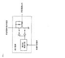
- FIG. FIG. 1 is a diagram showing a connection example of a system using the power switchgear according to Embodiment 1 of the present invention
- FIG. 2 is a diagram showing operation waveforms thereof.
- reference numeral 100 denotes a system
- a DC power source is drawn from a battery 10 through a connector 11 as a power source necessary for the operation of the system 100.
- a functional circuit (hereinafter referred to as a load) 14 serving as a load is connected to the power supply line constituted by the main circuits 12 and 13 of the system 100, and the current consumption during the operation of the load 14 is changed.
- a capacitor that is, a ripple capacitor 15 is connected.
- a power switch 16 is provided between the main circuit 12 and the main circuit 13 in order to supply and shut off the power to the load 14.
- the opening / closing of the power switch 16 and the operation of the boost power source 17 necessary for the operation of the power switch 16 are managed by the control means 18 using the operation of the microcontroller system.
- the power switch 16 is provided between the switch means 19 controlled by the control means 18, the slope waveform generating means 20 that performs the operation described later, and the enhancement type that performs the operation described later, between the main circuit 12 and the main circuit 13.
- the slope waveform generating means 20 includes a constant current source 24 connected between the boost power source 17 and the switch means 19, a series connection body of a capacitor 25 and a resistor 26 connected in parallel to the constant current source 24, and a constant current source 24.
- Reference numeral 28 denotes a switch connected to the battery 10.
- FIG. 1 shows the operating state of the switch 28
- (b) shows the operating state of the switch means 19
- (c) shows the operating state of the power switchgear 16
- (d) shows the passing current of the main circuits 4 and 5. Each is shown.
- the control means 18 when the switch 28 connected to the battery 10 is turned on, the control means 18 is activated. As shown in FIG. 2 (b), the control means 18 closes the switch means 19 provided in the power switchgear 16 as an initial state after startup, and then boosts the voltage as shown in FIG. 2 (c). The operation of the power supply 17 is started.
- the function of the step-up power supply 17 is to obtain a higher voltage than the operating power supply voltage of the system 100 obtained by taking in from the battery 10. This boosted voltage is supplied to the slope waveform generating means 20.
- the holding voltage of the capacitor 25 constituting the slope waveform generating means 20 holds the output voltage of the boost power supply 17 by closing the switch means 19 as an initial state.
- the control means 18 opens the operation of the switch means 19 provided in the power switching device 16 from the closed state. Switch to.
- the output current of the constant current source 24 provided inside the slope waveform generating means 20 flows into the capacitor 25 when the operation of the switch means 19 is opened, This is an operation for decreasing the holding voltage across the two ends in a slope shape.
- the output voltage Va of the boosting power supply 17 is stable, an operation in which the voltage Vb on the output side of the constant current source 24 increases from 0 V to the voltage Va as a result is obtained.
- the voltage Vb is applied to the gate of the enhancement type MOSFET 21 via the diode 27.
- the MOSFET 21 has a so-called source follower operation, and a voltage offset by a gate threshold voltage of the MOSFET 21 lower than the voltage applied to the gate is the source side, that is, the main side. It appears on the connection of the circuit 13. That is, the potential on the source side of the MOSFET 21 rises in a slope shape.
- the Zener diode 22 connected between the gate and source of the MOSFET 21 is provided for protection so that the gate application voltage of the MOSFET 21 becomes excessive after the power switchgear 16 is started up and the gate of the MOSFET 21 is not destroyed. Therefore, the Zener voltage may be selected based on the gate voltage characteristics of the MOSFET 21.
- the voltage applied to the gate of the MOSFET 21 is output from the constant current source 24, and the voltage clamped by the Zener diode 22 becomes the final gate drive voltage of the MOSFET 21, and during the steady closing operation of the power switching device 16, that is, the normal operation of the system 100. It will be in the middle state.
- the control means 18 changes the switch means 19 from open to closed, whereby the voltage Vb becomes zero.
- the diode 27 is cut off, and the electric charge remaining at the gate of the MOSFET 21 is discharged through the resistor 23, whereby the MOSFET 21 is turned off, that is, the power switching device 16 is turned off, as shown in FIG. It becomes.
- the charge of the ripple capacitor 15 is consumed and gradually discharged by the leak path of the load 14 or the like, but may be positively discharged by adding a bleeder resistor if necessary. .
- the MOSFET 21 serving as the switchgear of the power switchgear 16 shifts to the operating state due to the gradual increase of the output voltage when the power is turned on. To do.
- the charging current when the power supply rises for the ripple capacitor 15 provided on the load side of the power supply switching device 16 is appropriately controlled according to the gradually increasing gradient of the power supply voltage.
- the suppression of the rapid charging current (rush current) to the ripple capacitor 15 which has been a problem in the prior art by such an operation can be realized only by installing the power switch 16, so that the ripple capacitor 15 is precharged.
- the precharge circuit to be performed is not necessary, and the startup sequence can be simplified.
- Embodiment 2 a power switchgear according to Embodiment 2 of the present invention and a system using the same will be described.
- the increase rate of the output voltage of the MOSFET 21 may be set so as to increase with time.
- the allowable value of the charging current is limited by the loss characteristic (safe operation region) of the MOSFET 21 used as the power supply switching means.
- the operable time of the element varies depending on the energization current value, the drain-source voltage, and the energization time, and there is a restriction on the energizable region.
- the voltage between the drain and source increases, in addition to limiting due to the breakdown voltage of the element, secondary breakdown limitation considering breakdown due to malfunction of the parasitic element when the element generates heat, limitation due to limitation of temperature rise of the element due to drain loss, etc.
- the safe operation area is defined by time, ambient temperature, mounting conditions, and the like.
- the charging current locus is as shown by La in FIG.
- the drain-source voltage is high at the beginning of the rise, and operation in a region where the energization time is restricted becomes necessary.
- the increase rate of the drain output voltage of the MOSFET may be set to increase with time.
- the charging operation is performed along a locus such as Lb in FIG. 3, and there is a margin in the rating of the FET at the beginning of the rise. If the voltage difference between the drain and the source is gradually reduced and the charging current is reduced, the charging current is increased. Thus, the total charging time can be shortened while ensuring a margin as the operation of the FET.
- FIG. 4 is a diagram showing a connection example of a system using the power switch according to Embodiment 2 of the present invention. Note that the same or corresponding parts as those in the first embodiment are denoted by the same reference numerals, and the description thereof is omitted.
- the difference from the first embodiment is that the system 200 is pulled in from the downstream of the constant voltage power supply 40 performing a step-down operation from the battery power supply 10 and the MOSFET 21 serving as an opening / closing function of the power supply switchgear 41 as the operation power supply of the booster power supply 17.
- the power source is switched between the diodes 42 and 43, and the current waveform circuit is used as the configuration of the slope waveform generating means 20.
- the booster power source 17 for example, a charge pump circuit as shown in FIG. 5 can be used.
- a charge pump circuit as shown in FIG. 5 if the voltage loss of the diode or the switch is ignored, an output voltage twice as large as the input voltage can be obtained.
- a voltage twice as high as the output of the constant voltage power supply 40 for example, 5 v
- the operating power supply for the slope waveform generating means 20 can be obtained as the operating power supply for the slope waveform generating means 20.
- FIG. 6 is a diagram for explaining the operation of the system 200 using the power switching device 41 according to the second embodiment. 6, (a) shows the operating state of the switch 28, (b) shows the operating state of the switch means 19, (c) shows the operating state of the power switchgear 16, and (d) shows the passing current of the main circuits 4 and 5. Each is shown.
- the current determined mainly by the value of the resistor 44 and the output voltage of the boost power source 17 flows through the resistor 44 constituting the slope waveform generating means 20 with respect to the output of the boost power source 17.
- the capacitor 45 is charged by the value of the current flowing through the resistor 44, and the voltage Vb appearing at the lower end of the capacitor 45 is supplied to the MOSFET 21 via the NPN transistor 46 and the diode 27 as shown in FIG. Gradually increase the gate voltage.
- a voltage offset by the gate threshold voltage appears at the drain (main circuit 13) of the MOSFET 21, and the ripple capacitor 15 is charged.
- the main circuit 13 since the voltage of the main circuit 13 is supplied as the operating power supply of the boosting power supply 17 via the diode 43, if the voltage of the main circuit 13 becomes higher than the output of the constant voltage power supply 40, the main circuit 13 supplies the boosting power supply. 17 is supplied with electric power. As a result, the output voltage of the boost power supply 17 further increases.
- the charging current of the capacitor 45 constituting the slope waveform generating means 20 increases, the increase rate of the gate drive voltage of the MOSFET 21 increases with time, and the voltage increase rate of the main circuit 13 also increases with time. That is, the charging current of the ripple capacitor 15 increases with time, and the switch is closed, that is, the passing current trajectory of the MOSFET 21 operates like Lb in FIG. 3, so that a sufficient operation margin is secured in the safe operation region. Thus, it is possible to start up by charging the ripple capacitor 15 at high speed.
- the power switching device 41 according to the second embodiment and the system 200 using the power switching device 41 increase the increase rate of the output voltage of the MOSFET 21 in the transition operation from the power source closing to opening of the MOSFET 21 that opens and closes the power source. Since it is set so as to increase with time, the effect of the first embodiment and the effect of enabling high-speed startup within the allowable range of the transition operation of the MOSFET 21 are exhibited.
- Embodiment 3 a power switchgear according to Embodiment 3 of the present invention and a system using the same will be described.
- the semiconductor switch means using the MOSFET has been described.
- the transition from the power supply closed to the open can be operated by gradually increasing the output voltage by the action of the switch.
- the goal can be achieved. Therefore, the element to be employed is not limited to the MOSFET, and the same effect can be obtained even if, for example, a bipolar transistor is used.
- a configuration example of a system for realizing this embodiment will be described.
- FIG. 7 is a diagram illustrating a connection example of a system using the power switchgear according to the third embodiment.
- the same or corresponding parts as those in the first or second embodiment are denoted by the same reference numerals, and detailed description thereof is omitted.
- the voltage output from the slope waveform generating means 20 is input to the base via the base limiting resistor 72 of the bipolar transistor 71 as the semiconductor switch means. .
- the collector voltage changes according to the base voltage.
- the operation of the slope waveform generating means 20 for generating the base drive voltage waveform is the same as that of the second embodiment.
- the increase rate of the output voltage on the collector side of the bipolar transistor 71 increases with time, and similarly, the voltage increase rate of the main circuit 13 also increases with time.
- the charging current of the ripple capacitor 15 increases with time, and when the switch is closed, as in the case where the MOSFET of the second embodiment is used as a switch element, a sufficient operation margin is ensured in the safe operation region, and high speed is achieved. Activation by the charging operation to the ripple capacitor 15 becomes possible.
- Embodiment 4 FIG. Next, a power supply switching apparatus according to Embodiment 4 of the present invention will be described.
- the power switching function is normally performed when a normal voltage is applied to the system.
- an abnormal voltage is applied that causes reverse connection, the breakdown voltage of the switch element is insufficient and breaks down, or the phenomenon that the reverse voltage circulates inside the system via a parasitic element due to the semiconductor structure occurs. It is difficult to protect.
- a MOSFET for preventing current wraparound when the power source is reversely connected may be provided adjacent to the semiconductor switch means for opening and closing the power source.
- FIG. 8A is a diagram illustrating a connection example of a system using the power switching device according to the fourth embodiment.
- reference numeral 80A denotes a power switchgear according to Embodiment 4
- reference sign 400A denotes a system using the power switchgear 80A.
- a MOSFET 21 is used as a switching element, and a reverse connection protection MOSFET 81A for reverse power connection is connected adjacent to the MOSFET 21.
- the reverse connection protection MOSFET 81A has the body diode connected in the forward direction. Therefore, even if the gate-source voltage is 0V, the body diode has a forward voltage loss. Conducted.
- the gates of the MOSFET 21 serving as the switch means and the reverse connection protection MOSFET 81A are driven in common, they start up depending on the response of the MOSFET 21 at startup. After the rise, the gate-source applied voltages of both the MOSFET 21 and the reverse connection protection MOSFET 81A are sufficiently and sufficiently secured, so that the reverse connection protection MOSFET 81A is also turned on and becomes conductive. That is, an operation similar to that of the second embodiment is possible.
- the power supply switching device 80A can prevent the reverse polarity power supply from entering the circuit inside the system 400A.
- the operation of the power switch 80A is described focusing on the behavior when the power polarity is reversely connected.
- the power supply polarity of the constant voltage power supply 17 and the control means 18 is described.
- measures such as the addition of protective diodes are added to each function block as necessary, ensuring resistance to reverse polarity connection as a whole system. Of course it should be.
- FIG. 8B shows a different embodiment of the fourth embodiment.
- reference numeral 80B indicates a power switchgear and 400B indicates a system using the power switchgear 80B.
- the embodiment shown in FIG. 8B is a configuration example in which the switch element is a bipolar transistor 81B.
- the base drive of the bipolar transistor 81B and the gate of the reverse connection protection MOSFET 81A are driven by a common drive signal by using a base resistance series resistor 82, and the same operation as in FIG. 8A is realized.
- Other configurations and operations are the same as those in the case of FIG. 8A, and a description thereof will be omitted.
- the power switchgears 80A and 80B according to the fourth embodiment are realized with an easy configuration because the MOSFET 21 or the bipolar transistor 81B, which is generally readily available, is applied as the semiconductor switch unit that is the switchgear. Can do.
- the reverse connection protection MOSFET 81A for preventing the current from flowing when the power supply is reversely connected is provided adjacent to the MOSFET 21 or the bipolar transistor 81B for opening and closing the power supply, the load is prevented even when the power supply is reversely connected. It is also possible to prevent the current from flowing to 14 and to realize the protection characteristic against the reverse power connection, which is functionally similar to the mechanical relay.
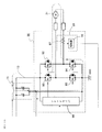
- FIG. 9 is a diagram for explaining the operation of the system using the power switchgear according to the fifth embodiment.
- a motor drive circuit using a PWM inverter circuit is connected as a load operated by a DC power supply.
- reference numeral 90 denotes a PWM inverter circuit.
- This PWM inverter circuit 90 is a so-called H-bridge type inverter, and the output between the two inverter output terminals is the rotation direction of the DC motor 91 and the conduction current. The size is changed. Therefore, if the DC motor of the permanent magnet field type brushed winding is used as the applied motor, for example, the output torque can be controlled according to the current value supplied to the DC motor 91.
- Reference numeral 500 denotes a system according to the fifth embodiment.
- an assist torque to be added to the steering system according to the detected torque of the torque sensor that detects the steering force is applied.
- An electric power steering device that is appropriately controlled by controlling the motor energization current and contributes to improvement in drivability can be considered.
- the configuration of FIG. 9 is configured by configuring the load 14 of FIG. 8A in the fourth embodiment as a PWM inverter circuit 90, and the power switch 80A performs the same startup procedure as described in the fourth embodiment. Then, supply of power to the PWM inverter circuit 90 which is a load is started.
- the control means 18 energizes the DC motor 91 through the FET driver means 96 between the gates and sources of the FETs 92, 93, 94, and 95 constituting the PWM inverter circuit 90.
- Appropriate PWM duty is selected at a frequency above the audible frequency upper limit according to the direction and magnitude of the power current.
- the motor drive current that actually flows is fed back to the control means 18 using the current detection means 99 including the current detection means 97 and the amplifier 98, thereby driving the DC motor 91 with a desired energization current and direction. Realize that.
- the current flow in the PWM inverter circuit 90 is considered.
- PWM powering that is, when a current flows from the power source to the DC motor 91, in the PWM pattern P of FIG. 10A, the FET 92 is turned on, the DC motor 91 is turned on, the FET 95 is turned on, and the state returns to GND.
- an instantaneous current supply from the ripple capacitor 15 is performed in order to follow a steep power supply current fluctuation in switching.
- the ripple capacitor 15 generally absorbs the fluctuation, and it is general to adopt a relatively large value as the ripple capacitor 15 with the intention of suppressing the fluctuation of the power supply current. Therefore, reducing the magnitude of the rush current when the power is turned on has a great effect by having the function to suppress the rush current in the power switching device 80A as in the present embodiment.
- the inverter arm composed of a pair of FETs 92 and 93 or FETs 94 and 95 constituting the PWM inverter circuit 90 is short-circuited against a reverse bias due to the presence of a parasitic diode of the FET.
- the protection by the power supply switching device 80A can be an effective means for preventing the PWM inverter circuit 90 from being destroyed.
- the PWM inverter circuit 90 has been described based on a simple H-bridge configuration.
- the PWM inverter circuit 90 is not limited to this configuration, for example, a three-phase bridge inverter.
- the power switchgear 80A is applied to the same problems as in the present embodiment, such as the treatment of ripple current associated with switching and the necessity of protection related to reverse connection, even in a multi-phase bridge circuit of more than that. Needless to say, it can be effective.
Landscapes
- Engineering & Computer Science (AREA)
- Power Engineering (AREA)
- Transportation (AREA)
- Mechanical Engineering (AREA)
- Direct Current Feeding And Distribution (AREA)
- Control Of Direct Current Motors (AREA)
- Power Conversion In General (AREA)
Abstract
Description
前記電源開閉装置の電源閉から開への遷移を前記半導体スイッチ手段の出力電圧の漸増により動作させ、前記コンデンサへの充電電流の値を抑制することを特徴とする。
この発明の前記以外の目的、特徴、観点及び効果は、図面を参照する以下のこの発明の詳細から、さらに明らかになるであろう。
図1は、この発明の実施の形態1に係る電源開閉装置を用いたシステムの接続例を示す図であり、図2はその動作波形を示す図である。
図1において、符号100はシステムを示し、このシステム100の動作に必要な電源として、バッテリ10からコネクタ11を介して直流電源が引き込まれている。システム100の主回路12、13によって構成された電源供給ラインには、負荷となる機能回路(以下、負荷という。)14が接続されており、この負荷14の動作時の消費電流の変動に対して主回路12、13の電圧を安定させるために、コンデンサ、即ちリプルコンデンサ15が接続されている。また、負荷14に対して電源の供給、遮断を行うために、主回路12と主回路13の間には電源開閉装置16が設けられている。この電源開閉装置16の開閉、及び電源開閉装置16の動作に必要な昇圧電源17の動作は、マイクロコントローラシステムの動作等を利用した制御手段18によって管理されている。
i=C・ΔV/Δt
となるから、スロープの傾きによって充電電流がコントロールできる。
次に、この発明の実施の形態2に係る電源開閉装置、及びそれを用いたシステムについて説明する。実施の形態1で説明したMOSFET21の電源閉から開への遷移動作において、MOSFET21の出力電圧の増加率を時間と共に大きくなるように設定しても良い。
実施の形態1の構成によれば、システム100の立ち上がり時にはリプルコンデンサ15に対して所定の電圧スロープが印加され、一定の充電電流が流れることで起動時のラッシュ電流の抑制を行うことが期待できるが、充電電流の許容値は電源開閉手段として用いたMOSFET21の損失特性(安全動作領域)によって制限をうけている。
実施の形態1と異なる点は、システム200において、昇圧電源17の動作電源として、バッテリ電源10から降圧動作をしている定電圧電源40及び電源開閉装置41の開閉機能となるMOSFET21の下流から引き込まれた電源を、ダイオード42及び43で切り替えて使用するものとし、また、スロープ波形発生手段20の構成として、カレントミラー回路を利用している点である。
図6において、(a)はスイッチ28の動作状態、(b)はスイッチ手段19の動作状態、(c)は電源開閉装置16の動作状態、(d)は主回路4、5の通過電流をそれぞれ示している。
次に、この発明の実施の形態3に係る電源開閉装置、及びそれを用いたシステムについて説明する。
実施の形態1あるいは実施の形態2においては、半導体スイッチ手段としてはMOSFETを利用するものを説明したが、スイッチの作用により電源閉から開への遷移を出力電圧の漸増により動作させることが出来れば目的は達成できる。従って、採用する素子としてはMOSFETに限定されるものではなく、例えばバイポーラトランジスタを使っても同様な効果を得ることができる。次に、この実施の形態を実現するためのシステムの構成例について説明する。
図7に示す実施の形態3において、実施の形態1あるいは実施の形態2と同一もしくは相当部分については、同一符号を付して詳細説明を省略する。
実施の形態3に係る電源開閉装置70を用いたシステム300においては、スロープ波形発生手段20から出力された電圧は、半導体スイッチ手段としてのバイポーラトランジスタ71のベース制限抵抗72を経てベースに入力される。バイポーラトランジスタ71はベース電圧に応じてコレクタ電圧が変化する。ベース駆動電圧波形を発生するスロープ波形発生手段20の動作は実施の形態2と同様である。電源開閉装置70の動作として、電源開から閉のとき、バイポーラトランジスタ71はコレクタ側の出力電圧の増加率が時間と共に増大し、同様に主回路13の電圧増加率も時間と共に増大する。
次に、この発明の実施の形態4に係る電源開閉装置について説明する。
実施の形態1から実施の形態3においては、電源の開閉を行う半導体スイッチ手段として、バイポーラトランジスタあるいはMOSFETを用いた例について説明した。これらの半導体スイッチ手段を用いると、電源開閉機能はシステムに対して正常な電圧が印加されている場合には電源の開閉の機能が正常に行われるが、対象のシステムに対して、電源の極性が逆接続となるような異常電圧の印加時にはスイッチ素子の耐圧が不足し破壊するか、あるいは半導体の構造上寄生素子を介して逆電圧がシステムの内部に回り込むと言う現象が発生し、システムを保護することは難しい。
図8Aにおいて、符号80Aは実施の形態4に係る電源開閉装置を示し、符号400Aは電源開閉装置80Aを用いたシステムを示している。実施の形態4においては、スイッチ素子としてMOSFET21を使用しており、このMOSFET21に隣接して電源逆接続に対する逆接保護用MOSFET81Aを接続している。電源の極性が正常な接続の状態においては、逆接保護用MOSFET81Aはボディダイオードが順方向の接続となっているため、ゲート・ソース間電圧が0Vであってもボディダイオードの順方向電圧の損失で導通している。スイッチ手段であるMOSFET21と逆接保護用MOSFET81Aのゲートは共通に駆動されているので、起動時はMOSFET21の応答に依存して立ち上がる。また、立ち上がり後はMOSFET21及び逆接保護用MOSFET81Aの両者のゲート・ソース間印加電圧が必要十分に確保されるので逆接保護用MOSFET81Aもオン状態となり、導通する。即ち、実施の形態2と同様な動作が可能である。
次に、この発明の実施の形態5に係る電源開閉装置、及びそれを用いたシステムについて説明する。図9は、実施の形態5に係る電源開閉装置を用いたシステムの動作を説明する図である。実施の形態5は直流電源により動作する負荷として、PWMインバータ回路によるモータ駆動回路を接続したものである。
図9において、符号90はPWMインバータ回路を示し、このPWMインバータ回路90は、所謂、Hブリッジタイプのインバータであって、インバータ出力2端子間の出力は、DCモータ91の回転方向と通電電流の大きさを変化させるものである。従って、適用モータとして、例えば永久磁石界磁式ブラシ付き巻線のDCモータを用いれば、DCモータ91に通電した電流値に応じて出力トルクの制御が可能となる。なお、符号500は実施の形態5に係るシステムを示している。
Claims (6)
- 直流電源により動作する機能回路の負荷電流の変動に対して供給電圧を安定化させるコンデンサを設けた電源供給ラインと、前記電源供給ラインの上流に位置する前記直流電源との間に、前記直流電源の開閉を行う半導体スイッチ手段を設け、前記機能回路に電源の供給、遮断を行う電源開閉装置であって、
前記電源開閉装置の電源閉から開への遷移を前記半導体スイッチ手段の出力電圧の漸増により動作させ、前記コンデンサへの充電電流の値を抑制することを特徴とする電源開閉装置。 - 前記電源開閉装置の電源閉から開への遷移において、前記半導体スイッチ手段の出力電圧の増加率を時間とともに大きくなるように設定したことを特徴とする請求項1に記載の電源開閉装置。
- 前記半導体スイッチ手段をバイポーラトランジスタ、もしくはMOSFETで構成したことを特徴とする請求項1又は請求項2に記載の電源開閉装置。
- 前記半導体スイッチ手段に隣接して、前記電源の逆接続による回り込み電流を阻止する保護用MOSFETを設けたことを特徴とする請求項3に記載の電源開閉装置。
- 前記機能回路は、モータを駆動するPWMインバータ回路であることを特徴とする請求項1から請求項4の何れか一項に記載の電源開閉装置。
- 請求項1から請求項5の何れか一項に記載の電源開閉装置と、直流電源により動作し、前記電源開閉装置を介して前記直流電源より供給電圧を得て動作する機能回路と、前記機能回路の負荷電流の変動に対して供給電圧を安定化させるコンデンサと、を備えたことを特徴とするシステム。
Priority Applications (5)
| Application Number | Priority Date | Filing Date | Title |
|---|---|---|---|
| EP14890692.8A EP3125391B1 (en) | 2014-04-29 | 2014-04-29 | Power switch device |
| PCT/JP2014/061923 WO2015166547A1 (ja) | 2014-04-29 | 2014-04-29 | 電源開閉装置及びそれを用いたシステム |
| CN201480078584.2A CN106463955B (zh) | 2014-04-29 | 2014-04-29 | 电源开关装置及使用该电源开关装置的系统 |
| US15/100,858 US9935480B2 (en) | 2014-04-29 | 2014-04-29 | Power switch device and system using same |
| JP2016515792A JP6169262B2 (ja) | 2014-04-29 | 2014-04-29 | 電源開閉装置及びそれを用いたシステム |
Applications Claiming Priority (1)
| Application Number | Priority Date | Filing Date | Title |
|---|---|---|---|
| PCT/JP2014/061923 WO2015166547A1 (ja) | 2014-04-29 | 2014-04-29 | 電源開閉装置及びそれを用いたシステム |
Publications (1)
| Publication Number | Publication Date |
|---|---|
| WO2015166547A1 true WO2015166547A1 (ja) | 2015-11-05 |
Family
ID=54358300
Family Applications (1)
| Application Number | Title | Priority Date | Filing Date |
|---|---|---|---|
| PCT/JP2014/061923 WO2015166547A1 (ja) | 2014-04-29 | 2014-04-29 | 電源開閉装置及びそれを用いたシステム |
Country Status (5)
| Country | Link |
|---|---|
| US (1) | US9935480B2 (ja) |
| EP (1) | EP3125391B1 (ja) |
| JP (1) | JP6169262B2 (ja) |
| CN (1) | CN106463955B (ja) |
| WO (1) | WO2015166547A1 (ja) |
Cited By (6)
| Publication number | Priority date | Publication date | Assignee | Title |
|---|---|---|---|---|
| JP2017135852A (ja) * | 2016-01-27 | 2017-08-03 | ミネベアミツミ株式会社 | モータ駆動制御装置及びそのモータ駆動制御方法 |
| CN107294366A (zh) * | 2016-03-31 | 2017-10-24 | 法雷奥汽车内部控制(深圳)有限公司 | 预充电电路、直流-直流转换器和混合动力汽车 |
| CN107306028A (zh) * | 2016-04-14 | 2017-10-31 | 安德烈·斯蒂尔股份两合公司 | 识别运行开关的开关位置使电动机投入运行的方法和装置 |
| JP2018191370A (ja) * | 2017-04-28 | 2018-11-29 | 株式会社デンソー | 電源装置 |
| JP2018196115A (ja) * | 2017-05-16 | 2018-12-06 | コンチネンタル オートモーティヴ ゲゼルシャフト ミット ベシュレンクテル ハフツングContinental Automotive GmbH | 電子モジュールおよび自動車ならびにモジュールのスイッチオン過程中の入力電流を制限する方法 |
| US20210074489A1 (en) * | 2019-09-09 | 2021-03-11 | Andreas Stihl Ag & Co. Kg | Method for operating an electrical treatment device and electrical treatment device |
Families Citing this family (15)
| Publication number | Priority date | Publication date | Assignee | Title |
|---|---|---|---|---|
| JP6656186B2 (ja) * | 2017-01-11 | 2020-03-04 | 株式会社東芝 | 回生電流検出回路、チャージ電流検出回路、モータ電流検出システム |
| CN106972792B (zh) * | 2017-04-27 | 2023-08-18 | 上海灿瑞科技股份有限公司 | 一种h桥驱动电路 |
| CN109687541A (zh) * | 2017-10-19 | 2019-04-26 | 新盛力科技股份有限公司 | 电池供电装置 |
| US11373828B2 (en) * | 2018-03-23 | 2022-06-28 | Panasonic Intellectual Property Management Co., Ltd. | Electromagnetic relay and control method thereof |
| JP2020031486A (ja) * | 2018-08-22 | 2020-02-27 | 株式会社マキタ | 電圧供給装置 |
| US11522363B2 (en) * | 2018-09-03 | 2022-12-06 | Stmicroelectronics S.R.L. | Supply protection circuit that protects power transistor from a supply signal of an incorrect polarity |
| US11545824B2 (en) * | 2018-10-11 | 2023-01-03 | Texas Instruments Incorporated | USB short circuit protection |
| CN110962630B (zh) * | 2018-12-04 | 2021-06-25 | 宁德时代新能源科技股份有限公司 | 预充电流的调控方法和电路 |
| US11539201B2 (en) * | 2019-03-04 | 2022-12-27 | Portwell Inc. | Reverse polarity protection device |
| CN110588438B (zh) * | 2019-09-18 | 2024-04-30 | 深圳市科列技术股份有限公司 | 汽车电池管理系统主动均衡矩阵开关的供电及驱动电路 |
| JP2021048747A (ja) * | 2019-09-20 | 2021-03-25 | 日本電産トーソク株式会社 | 回路基板、及び電動オイルポンプ |
| CN113131730B (zh) * | 2019-12-30 | 2023-12-19 | 台达电子工业股份有限公司 | 预充电控制电路及其控制方法 |
| CN113740653B (zh) * | 2021-09-08 | 2022-07-29 | 无锡力芯微电子股份有限公司 | 适用于ldo动态负载响应的高精度评估方法及电路 |
| CN115995801A (zh) * | 2023-02-09 | 2023-04-21 | 上海拿森汽车电子有限公司 | 用于车身稳定系统的功率供电装置、系统及车辆 |
| CN115864843B (zh) * | 2023-02-27 | 2023-05-02 | 深圳飞骧科技股份有限公司 | 一种多电源切换电路结构及电子设备 |
Citations (6)
| Publication number | Priority date | Publication date | Assignee | Title |
|---|---|---|---|---|
| JPH07147767A (ja) * | 1993-11-22 | 1995-06-06 | Sanden Corp | モータ駆動装置の電源制御装置 |
| JPH11122813A (ja) * | 1997-10-09 | 1999-04-30 | Nec Corp | 電源電圧印加方法及びその回路 |
| JP2005223804A (ja) * | 2004-02-09 | 2005-08-18 | Harison Toshiba Lighting Corp | スイッチ回路 |
| JP2010049482A (ja) * | 2008-08-21 | 2010-03-04 | Sharp Corp | 直流安定化電源装置 |
| JP2011018195A (ja) * | 2009-07-09 | 2011-01-27 | Toshiba Corp | 電源回路及び電子機器 |
| JP2014030317A (ja) * | 2012-07-31 | 2014-02-13 | Furuno Electric Co Ltd | 逆接続保護回路、及びこれを備えた電子機器 |
Family Cites Families (11)
| Publication number | Priority date | Publication date | Assignee | Title |
|---|---|---|---|---|
| US6870279B2 (en) * | 1998-01-05 | 2005-03-22 | Capstone Turbine Corporation | Method and system for control of turbogenerator power and temperature |
| US7019583B2 (en) * | 2001-01-29 | 2006-03-28 | Axiohm Transaction Solutions, Inc. | Current inrush limiting circuit |
| ITTO20020263A1 (it) | 2002-03-25 | 2003-09-25 | Sila Holding Ind Spa | Circuito di interfaccia fra una sorgente di tensione continua ed un circuito di pilotaggio di un carico,particolarmente per l'impiego a bord |
| JP3989352B2 (ja) | 2002-10-08 | 2007-10-10 | 本田技研工業株式会社 | モータ駆動装置 |
| US7642677B2 (en) * | 2007-08-02 | 2010-01-05 | Motorola, Inc. | Controlling inrush current from a power supply to a load |
| JP5200986B2 (ja) * | 2009-02-17 | 2013-06-05 | 新神戸電機株式会社 | 電源装置 |
| WO2010150488A1 (ja) * | 2009-06-24 | 2010-12-29 | パナソニック株式会社 | 電源保護回路およびそれを備えたモータ駆動装置 |
| JP2011188647A (ja) * | 2010-03-09 | 2011-09-22 | Toshiba Corp | Dc/dcコンバータ |
| EP2544371A1 (en) * | 2011-07-08 | 2013-01-09 | Dialog Semiconductor GmbH | Slew rate PWM controlled charge pump for limited in-rush current switch driving |
| US8917064B2 (en) * | 2012-06-20 | 2014-12-23 | International Business Machines Corporation | Control circuit for power distribution switch |
| CN104702097B (zh) * | 2013-12-04 | 2017-11-24 | 台达电子企业管理(上海)有限公司 | 电源装置和通过电源装置产生电源的方法 |
-
2014
- 2014-04-29 JP JP2016515792A patent/JP6169262B2/ja not_active Expired - Fee Related
- 2014-04-29 US US15/100,858 patent/US9935480B2/en active Active
- 2014-04-29 EP EP14890692.8A patent/EP3125391B1/en active Active
- 2014-04-29 WO PCT/JP2014/061923 patent/WO2015166547A1/ja active Application Filing
- 2014-04-29 CN CN201480078584.2A patent/CN106463955B/zh not_active Expired - Fee Related
Patent Citations (6)
| Publication number | Priority date | Publication date | Assignee | Title |
|---|---|---|---|---|
| JPH07147767A (ja) * | 1993-11-22 | 1995-06-06 | Sanden Corp | モータ駆動装置の電源制御装置 |
| JPH11122813A (ja) * | 1997-10-09 | 1999-04-30 | Nec Corp | 電源電圧印加方法及びその回路 |
| JP2005223804A (ja) * | 2004-02-09 | 2005-08-18 | Harison Toshiba Lighting Corp | スイッチ回路 |
| JP2010049482A (ja) * | 2008-08-21 | 2010-03-04 | Sharp Corp | 直流安定化電源装置 |
| JP2011018195A (ja) * | 2009-07-09 | 2011-01-27 | Toshiba Corp | 電源回路及び電子機器 |
| JP2014030317A (ja) * | 2012-07-31 | 2014-02-13 | Furuno Electric Co Ltd | 逆接続保護回路、及びこれを備えた電子機器 |
Non-Patent Citations (1)
| Title |
|---|
| See also references of EP3125391A4 * |
Cited By (8)
| Publication number | Priority date | Publication date | Assignee | Title |
|---|---|---|---|---|
| JP2017135852A (ja) * | 2016-01-27 | 2017-08-03 | ミネベアミツミ株式会社 | モータ駆動制御装置及びそのモータ駆動制御方法 |
| CN107294366A (zh) * | 2016-03-31 | 2017-10-24 | 法雷奥汽车内部控制(深圳)有限公司 | 预充电电路、直流-直流转换器和混合动力汽车 |
| CN107306028A (zh) * | 2016-04-14 | 2017-10-31 | 安德烈·斯蒂尔股份两合公司 | 识别运行开关的开关位置使电动机投入运行的方法和装置 |
| CN107306028B (zh) * | 2016-04-14 | 2020-04-07 | 安德烈·斯蒂尔股份两合公司 | 识别运行开关的开关位置使电动机投入运行的方法和装置 |
| JP2018191370A (ja) * | 2017-04-28 | 2018-11-29 | 株式会社デンソー | 電源装置 |
| JP2018196115A (ja) * | 2017-05-16 | 2018-12-06 | コンチネンタル オートモーティヴ ゲゼルシャフト ミット ベシュレンクテル ハフツングContinental Automotive GmbH | 電子モジュールおよび自動車ならびにモジュールのスイッチオン過程中の入力電流を制限する方法 |
| US20210074489A1 (en) * | 2019-09-09 | 2021-03-11 | Andreas Stihl Ag & Co. Kg | Method for operating an electrical treatment device and electrical treatment device |
| US11651911B2 (en) * | 2019-09-09 | 2023-05-16 | Andreas Stihl Ag & Co. Kg | Method for operating an electrical treatment device and electrical treatment device |
Also Published As
| Publication number | Publication date |
|---|---|
| EP3125391A1 (en) | 2017-02-01 |
| JPWO2015166547A1 (ja) | 2017-04-20 |
| CN106463955A (zh) | 2017-02-22 |
| US9935480B2 (en) | 2018-04-03 |
| JP6169262B2 (ja) | 2017-07-26 |
| EP3125391A4 (en) | 2017-10-18 |
| US20160301235A1 (en) | 2016-10-13 |
| CN106463955B (zh) | 2020-01-21 |
| EP3125391B1 (en) | 2020-02-19 |
Similar Documents
| Publication | Publication Date | Title |
|---|---|---|
| JP6169262B2 (ja) | 電源開閉装置及びそれを用いたシステム | |
| US9490732B2 (en) | Power conversion apparatus, electronic steering system, electric vehicle, electronic control throttle and power brake | |
| JP3884450B2 (ja) | 電動パワーステアリング装置 | |
| JP2003244943A (ja) | 電源装置の昇圧装置 | |
| KR101704112B1 (ko) | 모터 구동 장치 | |
| JP2007306710A (ja) | 電動パワーステアリング装置 | |
| WO2015016034A1 (ja) | 電動モータの駆動装置及び駆動方法 | |
| JP6091632B2 (ja) | 電力変換装置 | |
| JP2009055078A (ja) | 負荷駆動回路 | |
| KR101721616B1 (ko) | 모터의 구동 제어 장치 및 방법 | |
| US9148055B2 (en) | Power system with electronic impedance switch controls and methods for supplying power to a load | |
| US10840899B2 (en) | Motor drive device and electric power steering device | |
| JP2007027465A (ja) | リニアソレノイドの駆動回路 | |
| JP2005158870A (ja) | 負荷制御装置 | |
| JP2007019293A (ja) | リニアソレノイドの駆動装置 | |
| CN110435751B (zh) | 电动转向的控制 | |
| JP5715363B2 (ja) | 誘導性負荷駆動装置 | |
| JP7389701B2 (ja) | 電源回路、電源供給方法 | |
| JP2017017688A (ja) | 電界効果トランジスタを備えたパワー半導体回路 | |
| KR100527528B1 (ko) | 모터 구동 장치 | |
| JP2023053563A (ja) | 電力供給装置 | |
| JP5492009B2 (ja) | 負荷制御装置 | |
| CN113381386A (zh) | 包括恒定功率控制器的电气开关系统及相关方法 | |
| KR20140073800A (ko) | 전자식 릴레이용 회로 | |
| JP2003133928A (ja) | 負荷駆動回路 |
Legal Events
| Date | Code | Title | Description |
|---|---|---|---|
| 121 | Ep: the epo has been informed by wipo that ep was designated in this application |
Ref document number: 14890692 Country of ref document: EP Kind code of ref document: A1 |
|
| ENP | Entry into the national phase |
Ref document number: 2016515792 Country of ref document: JP Kind code of ref document: A |
|
| WWE | Wipo information: entry into national phase |
Ref document number: 15100858 Country of ref document: US |
|
| REEP | Request for entry into the european phase |
Ref document number: 2014890692 Country of ref document: EP |
|
| WWE | Wipo information: entry into national phase |
Ref document number: 2014890692 Country of ref document: EP |
|
| NENP | Non-entry into the national phase |
Ref country code: DE |