WO2015136830A1 - 光学デバイスおよびその製造方法 - Google Patents
光学デバイスおよびその製造方法 Download PDFInfo
- Publication number
- WO2015136830A1 WO2015136830A1 PCT/JP2015/000414 JP2015000414W WO2015136830A1 WO 2015136830 A1 WO2015136830 A1 WO 2015136830A1 JP 2015000414 W JP2015000414 W JP 2015000414W WO 2015136830 A1 WO2015136830 A1 WO 2015136830A1
- Authority
- WO
- WIPO (PCT)
- Prior art keywords
- base
- optical
- optical element
- wall
- window
- Prior art date
Links
Images


Classifications
-
- G—PHYSICS
- G02—OPTICS
- G02B—OPTICAL ELEMENTS, SYSTEMS OR APPARATUS
- G02B26/00—Optical devices or arrangements for the control of light using movable or deformable optical elements
- G02B26/08—Optical devices or arrangements for the control of light using movable or deformable optical elements for controlling the direction of light
- G02B26/10—Scanning systems
- G02B26/105—Scanning systems with one or more pivoting mirrors or galvano-mirrors
-
- G—PHYSICS
- G02—OPTICS
- G02B—OPTICAL ELEMENTS, SYSTEMS OR APPARATUS
- G02B26/00—Optical devices or arrangements for the control of light using movable or deformable optical elements
- G02B26/08—Optical devices or arrangements for the control of light using movable or deformable optical elements for controlling the direction of light
- G02B26/0816—Optical devices or arrangements for the control of light using movable or deformable optical elements for controlling the direction of light by means of one or more reflecting elements
- G02B26/0833—Optical devices or arrangements for the control of light using movable or deformable optical elements for controlling the direction of light by means of one or more reflecting elements the reflecting element being a micromechanical device, e.g. a MEMS mirror, DMD
- G02B26/0858—Optical devices or arrangements for the control of light using movable or deformable optical elements for controlling the direction of light by means of one or more reflecting elements the reflecting element being a micromechanical device, e.g. a MEMS mirror, DMD the reflecting means being moved or deformed by piezoelectric means
-
- G—PHYSICS
- G02—OPTICS
- G02B—OPTICAL ELEMENTS, SYSTEMS OR APPARATUS
- G02B27/00—Optical systems or apparatus not provided for by any of the groups G02B1/00 - G02B26/00, G02B30/00
- G02B27/0006—Optical systems or apparatus not provided for by any of the groups G02B1/00 - G02B26/00, G02B30/00 with means to keep optical surfaces clean, e.g. by preventing or removing dirt, stains, contamination, condensation
Definitions
- the present invention relates to an optical device in which an optical element having a rotatable optical function surface is disposed inside a package, and a manufacturing method thereof.
- an optical device has a housing having a recess for accommodating an optical element, and a lid disposed at an opening portion of the housing. A transparent window is formed on the lid.
- the housing and the lid are joined with low melting point glass or the like.
- Another optical device has a package member in which an optical element is arranged and a metal cap in which a window portion is integrated. The cap is provided on the base substrate and accommodates the optical element inside the metal cap. Then, the metal cap and the base substrate are seam welded. With these structures, in the conventional optical device, the inside that houses the optical element is sealed.
- Patent Document 1 and Patent Document 2 are known.
- Such an optical device has a problem that the characteristics of the optical element and the optical device are deteriorated in the manufacturing process. Therefore, it is desired to reduce the deterioration of the characteristics of the optical element and the optical device.
- An optical device includes an optical element having a rotatable optical function surface, a base that supports the optical element, and a package that houses the optical element and the base.
- the package seals the wall portion that surrounds the optical element and the base, a transparent window portion that seals one opening portion of the wall portion and forms an optical path to the optical functional surface, and the other opening portion of the wall portion.
- a bottom plate a bottom plate.
- the optical device according to the present disclosure can reduce characteristic deterioration in the manufacturing process of the optical device and the optical element.
- FIG. 1 is an exploded perspective view of an optical device according to an embodiment of the present disclosure.
- FIG. 2 is a schematic diagram illustrating a usage state of the optical device according to the present disclosure.
- FIG. 3 is a front view of the optical element of the optical device according to the present disclosure.
- FIG. 4 is a schematic diagram illustrating a method for manufacturing an optical device according to the present disclosure.
- FIG. 5 is a schematic diagram illustrating a structure in which an optical element and a base in an optical device according to the present disclosure are integrated.
- FIG. 6 is a schematic diagram illustrating a state in which the base according to the present disclosure is disposed in the wall portion.
- FIG. 7 is a schematic diagram illustrating a method for limiting the displacement of the optical element in the base according to the present disclosure.
- FIG. 8 is a front view of an optical element according to another embodiment of the present disclosure.
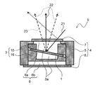
- FIG. 1 is a diagram showing an optical scanning device 9 which is an example of an optical device
- FIG. 2 is a schematic diagram showing a use state thereof.
- the optical scanning device 9 controls the reflection angle of the incident light 21 incident on the optical scanning device 9 by controlling the rotation of the reflecting surface of the optical element 1, and scans the outgoing light 22 within a predetermined region.
- Package 4 includes a window portion 7, a wall portion 5, and a bottom plate 8.
- the optical element 1 is arranged in the package 4 through the base 3. Thereby, the optical element 1 is in a rotatable state.
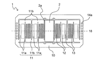
- the optical element 1 includes a movable plate 2 a having an optical function surface 2, a pair of vibrating beams 11 arranged so as to extend along the rotation shaft 18 of the movable plate 2 a, and the pair of vibrating beams 11.
- the frame-shaped fixed portion 10 that supports the movable plate 2a is provided. That is, the vibrating beam 11 has one end supported by the fixed portion 10 and the other end connected to the movable plate 2 a having the optical function surface 2.
- the optical function surface 2 is, for example, a reflection surface.
- the vibrating beam 11 has a meander-shaped structure in which a plurality of straight portions 11a and folded portions 11b are connected. Each linear portion 11a is provided with a driving unit 12 that applies vertical vibration to the linear portion 11a.
- the drive unit 12 is a laminated structure in which a piezoelectric layer is disposed between an upper electrode and a lower electrode (not shown), for example.
- the drive part 12 can bend and vibrate the linear part 11a to an up-down direction by applying a control voltage between an upper electrode and a lower electrode.
- the optical scanning device 9 can rotate the movable plate 2a around the rotation shaft 18 by bending the drive unit 12 disposed in the adjacent linear portion 11a in the reverse direction.
- the monitor unit 13 is disposed along the drive unit 12 in the straight line part 11a.
- the monitor unit 13 has the same structure as the drive unit 12.
- the monitor unit 13 generates a waveform signal from the vibration generated in the straight line part 11a.
- the generated waveform signal is used for driving control of the movable plate 2a.
- the drive unit 12 and the monitor unit 13 are each connected to an electrode pad 14a disposed on the fixed unit 10 by a wiring unit (not shown).
- the optical element 1 has a flat plate structure formed by a MEMS (Micro Electro Mechanical Systems) process.
- the optical element 1 is formed using shape processing by dry etching on a Si substrate, film formation by sputtering, pattern formation by etching, and the like.
- the base 3 is provided with a recess 3a for providing a space in a portion corresponding to a vibration region between the vibrating beam 11 and the movable plate 2a.
- the base 3 supports the optical element 1 with a fixing portion 10 located on the outer peripheral portion. That is, the base 3 is connected to the fixed portion 10.
- the base 3 has a suspension structure that allows the vibrating beam 11 and the movable plate 2a to be rotated.
- the package 4 includes a cylindrical wall portion 5 having openings at both ends, a window portion 7 for sealing one opening portion 6, and a bottom plate 8 for sealing the other opening portion 6.
- the optical element 1 and the base 3 are accommodated in a package 4.
- the wall portion 5 is disposed so as to surround the outer periphery of the optical element 1 and the base 3.
- the base 3 is supported by the wall 5.
- the wall 5 is formed of ceramics or the like.
- the window portion 7 seals the opening 6 a on the optical path side of the incident light 21 and the emitted light 22 among the plurality of openings 6 provided in the wall portion 5.
- the window part 7 is provided on the optical path and has translucency.
- the window part 7 is formed of optical glass.
- the wall part 5 and the window part 7 are integrated with the low melting glass.
- the bottom plate 8 seals the opening 6 b on the side opposite to the window 7 in the opening 6 of the wall 5.
- the bottom plate 8 is formed of a metal plate.
- the baseplate 8 is integrated with the end surface of the wall part 5 by seam welding.
- the sealing process at the opening 6 of the package 4 includes two steps.
- One step is a step of bonding the window portion 7 and the wall portion 5 using low melting point glass and sealing the opening portion 6a.
- the other step is a step of welding the wall 5 and the bottom plate 8 by seam welding and sealing the opening 6b.
- the temperature of the heat treatment in the bonding step with the low melting point glass is about 600 degrees.
- the heat treatment in the bonding process affects the entire package 4 by heat.
- the seam welding process is characterized in that although the heat treatment temperature is high, the influence of heat on the surroundings is small because the heated part is the part to be welded. Therefore, the optical scanning device 9 can reduce the deterioration of characteristics in the manufacturing process by dividing the sealing step into two steps as described above.
- FIG. 4 shows the sealing process of the package 4 of the optical scanning device 9.
- the window portion 7 is disposed in the opening 6 a of the wall portion 5. And the wall part 5 and the window part 7 are adhere
- the optical element 1 and the base 3 are integrated as an assembly 27.
- the assembled body 27 is inserted into the wall portion 5 in which the opening 6 a is sealed by the window portion 7, and the assembled 27 and the wall portion 5 are connected.
- the bottom plate 8 is disposed in the opening 6b of the wall 5, and the bottom plate 8 and the end surface of the opening 6b of the wall 5 are integrated by seam welding 8a.
- the adhesion by the low melting point glass 7a having a large influence of heat is performed before the optical element 1 is inserted. Therefore, it is possible to prevent the optical element 1 from being affected by the heat treatment process of bonding using the low melting point glass 7a. Thereafter, the sealing process by the bottom plate 8 in a state where the optical element 1 is arranged is performed by the seam welding 8a having a small range of influence of heat. Thereby, the characteristic deterioration accompanying the heat processing of the optical element 1 arrange
- a lead zirconate titanate (PZT) thin film is used as the piezoelectric layer constituting the drive unit 12.
- the PZT thin film is liable to deteriorate characteristics due to high temperature processing. For this reason, the above-described configuration can further suppress the influence of the heat treatment.
- the window portion 7 is made of optical glass
- the wall portion 5 is made of ceramics.
- Optical glass and ceramics have close thermal expansion coefficients. Therefore, since the difference in expansion / contraction amount in the heat treatment between the window portion 7 and the wall portion 5 is small, internal stress remaining after the heat treatment process can be suppressed. As a result, it is possible to suppress deterioration of the characteristics of the optical scanning device 9 due to a heat treatment process such as deformation of the window 7 and generation of cracks due to internal stress.
- a metal material such as Kovar may be used as the wall portion 5.
- the difference in thermal expansion from the optical glass forming the window portion 7 becomes large, and the heat shrinkage stress of the wall portion 5 made of metal acts on the window portion 7 even in the heat treatment of seam welding.
- the thermal contraction stress causes deterioration of the flatness of the window portion 7 and generation of cracks in the window portion 7.
- the deterioration of the flatness of the window part 7 adversely affects the incident light beam and the outgoing light beam.
- the crack which arises in the window part 7 causes the fall of the airtightness of the package 4. Therefore, in order to reduce the influence of heat shrinkage stress, it is necessary to make the seam welded portion of the wall portion 5 away from the optical glass. In this case, the entire package becomes large, and the cost increases accordingly.
- the influence of the heat shrinkage stress caused by seam welding can be reduced by forming the window portion 7 with optical glass and the wall portion 5 with ceramics. Therefore, the optical scanning device 4 can narrow the distance between the seam welded portion and the window portion 7, and as a result, the optical scanning device can be miniaturized.
- the optical scanning device 9 has a structure in which the optical element 1 is connected to the wall portion 5 through the base 3.
- the welded portion has a structure that does not come into contact with the base 3, the influence of heat exerted on the optical element 1 by the seam welding 8 a can be reduced.
- the base 3 has a divided structure including a first base 15 and a second base 16.
- the first base 15 is disposed closer to the window part 7 than the optical element 1.
- the first base 15 is supported by the wall portion 5.
- the first base 15 has a region that transmits light at a position corresponding to the optical function surface 2. This region is formed of a light transmissive material. Note that the light transmitting region may be a through hole provided in the first base.
- the second base 16 is disposed on the bottom plate 8 side.
- a control signal path from the optical element 1 to the outside of the package 4 is provided so as to be connected to the wall portion 5 from the optical element 1 via the second base 16.
- FIG. 5 is a schematic diagram showing a structure in which the optical element 1 and the second base 16 are integrated.
- the optical element 1 is disposed on the second base 16. Then, the electrode pad 14a provided on the optical element 1 and the electrode pad 14b provided on the second base 16 are connected by wire bonding. Next, the first base 15 is disposed on the second base 16 so as to cover the optical element 1, and the base 3 and the optical element 1 are integrated as an assembly 27. The integrated assembly 27 is inserted into the wall portion 5 to which the window portion 7 is bonded as shown in FIG.
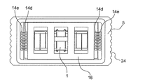
- FIG. 6 is a plan view of the wall 5 into which the assembly 27 is inserted as viewed from the opening 6b side.
- an electrode pad 14 d exposed on the back side of the second base 16 is provided in the opening 6 b of the wall 5.
- the electrode pad 14d is connected to the electrode pad 14b via the wraparound electrode 14c shown in FIG.
- the wall 5 is provided with an electrode pad 14e on the inner side.
- the electrode pad 14d is connected to the electrode pad 14e by wire bonding.
- the wall portion 5 has an internal electrode (not shown).
- the electrode pad 14e is connected to a side electrode 24 provided on the outer peripheral surface of the wall portion 5 via an internal electrode.
- the control signal path connected to the optical element 1 is configured by a path from the wall portion 5 to the optical element 1 via the second base 16.
- the base 3 is a divided structure including the first base 15 and the second base 16.
- the optical element 1 is provided between the first base 15 and the second base 16. And the optical element 1 is arrange
- the bonding plane between the base 3 and the optical element 1 is provided non-parallel to the incident surface of the window portion 7 for the incident light 21.
- a joining plane between the base 3 and the optical element 1 is a surface formed by a split surface of the base 3.
- the dividing surface of the base 3 means a bonding surface between the first base 15 and the optical element 1 and a bonding surface between the second base 16 and the optical element 1.
- the optical element 1 and the window portion 7 are provided in parallel, the direction of the surface reflected light 23 and the direction of the emitted light 22 from the optical element 1 are approximated, and the surface reflected light 23 is emitted through the optical element 1. It appears as noise in the scanning area of the emitted light 22. Therefore, it is possible to prevent the surface reflected light 23 from appearing as noise by providing the optical element 1 and the window portion 7 in non-parallel.
- FIG. 7 is a cross-sectional view showing a modification of the optical scanning device 9.
- the optical element 1 is sandwiched between the first base 15 and the second base 16.
- the first base 15 and the second base 16 are formed with contact portions 25 that limit the displacement of the movable plate 2a of the optical element 1 on the inner surface. Thereby, it is possible to prevent the optical element 1 from being damaged by the deformation of the vibrating beam 11 due to a strong impact or the like.
- the contact portion 25 is provided at a position that does not overlap the movable range 26 so as not to hinder the rotation of the movable plate 2a indicated by a broken line. It is desirable that the contact portion 25 is closest to the movable plate 2 a on the rotation shaft 18. Further, in a portion other than the vicinity of the rotating shaft 18, the minimum necessary gap that does not affect the rotating frequency or amplitude is generated around the contact portion 25 without increasing the air resistance due to the rotating of the movable plate 2 a. It is desirable to be secured.
- the optical scanning device 9 may have a configuration using a biaxial scanning optical element as shown in FIG.
- the optical element 28 is provided with a movable frame 17 at the position of the movable plate 2a in FIG.
- the movable frame 17 is connected to the vibrating beam 11.
- the vibrating beam 11 corresponds to the first vibrating beam.
- the movable frame 17 has the second vibrating beam 19 and the optical function surface 2 on the inner side.
- the second vibrating beam 19 has a second rotating shaft 20 that is orthogonal to the rotating shaft 18.
- the second vibrating beam 19 has one end connected to the movable frame 17 and the other end connected to the movable plate 2a. That is, the movable plate 2a is connected to a pair of second vibrating beams 19 having the second rotation shaft 20 as a rotation center. At this time, the rotation shaft 18 corresponds to the first rotation shaft.
- the movable plate 2 a is connected to the inner end of the second vibrating beam 19.
- An optical functional surface 2 is disposed on the movable plate 2a.
- the first vibrating beam 11 is provided with a first driving unit
- the second vibrating beam 19 is provided with a second driving unit.
- Each of the first driving unit and the second driving unit includes an upper electrode, a lower electrode, and a piezoelectric layer disposed between the upper electrode and the lower electrode.
- the optical scanning device in which the reflecting surface is formed on the movable plate 2a as the optical function surface 2 has been described as an example.
- the optical element may form a light detection surface made of a pyroelectric film on the movable plate 2 a as the optical function surface 2.
- An optical device using an optical element having a light detection surface can be used as a light detection device.
- the present disclosure can be applied to an optical device in which the optical element 1 having the rotatable optical function surface 2 is disposed inside the package 4.
- the optical device in the present embodiment includes an optical element having a rotatable optical function surface, a base that supports the optical element, and a package that houses the optical element and the base.
- a wall that surrounds the optical element and the base, a translucent window that seals one opening of the wall and forms an optical path to the optical functional surface, and a bottom plate that seals the other opening of the wall An optical device.
- the optical element includes a fixed portion connected to the base, a vibrating beam having one end supported by the fixed portion and the other end connected to a movable plate having an optical functional surface,
- a drive unit that vibrates the vibrating beam, and the drive unit may include an upper electrode, a lower electrode, and a piezoelectric layer disposed between the upper electrode and the lower electrode.
- the window portion is formed of optical glass
- the wall portion is formed of ceramics
- the bottom plate is formed of a metal plate
- the window portion and the wall portion are connected with low-melting glass.
- the wall portion and the bottom plate may be welded.
- the base may be supported by a wall portion.
- the base includes a divided structure including a first base provided on the window portion side of the optical element and a second base provided on the bottom plate side, and the first base is a wall.
- the control signal path supported by the section and connected to the optical element may be configured as a path from the wall section to the optical element via the second base.
- the bonding plane formed at the connection point between the optical element and the first base or the second base may be non-parallel to the window portion.
- the first base and the second base may limit the displacement of the optical element.
- the optical functional surface may be a reflective surface.
- the optical function surface may be a light detection surface.
- the optical element includes a fixed portion connected to the base, a first vibrating beam having one end connected to the fixed portion and the other end connected to the movable frame, A first drive unit that vibrates the vibrating beam, and the movable frame has a movable plate having an optical functional surface, one end connected to the movable frame and the other end connected to the movable plate, and the first A second vibration beam having a second rotation axis different from the first rotation axis of the vibration beam; and a second drive unit that vibrates the second vibration beam, the first drive unit and Each of the second drive units may include an upper electrode, a lower electrode, and a piezoelectric layer disposed between the upper electrode and the lower electrode.
- an optical device manufacturing method includes an optical element having a rotatable optical function surface, a base that supports the optical element, and a package that houses the optical element and the base.
- the package includes a wall portion that surrounds the optical element and the base, a translucent window portion that forms an optical path to the optical functional surface and seals one opening portion of the wall portion, and the other of the wall portion.
- the method of manufacturing an optical device includes a step of arranging a window in one opening of the wall and bonding with a low-melting glass, and integrating the optical element with the base A step of connecting the base integrated with the optical element to the wall integrated with the process, and the other opening of the wall integrated with the base integrated with the optical element and the window Place the bottom plate on the seat And a step of joining by welding, the.
- the optical device according to one or more aspects has been described based on the embodiment, but the present disclosure is not limited to this embodiment. Unless it deviates from the gist of the present disclosure, various modifications conceived by those skilled in the art have been made in this embodiment, and forms constructed by combining components in different embodiments are also within the scope of one or more aspects. May be included.
- This disclosure is effective in optical devices such as in-vehicle use.
Landscapes
- Physics & Mathematics (AREA)
- General Physics & Mathematics (AREA)
- Optics & Photonics (AREA)
- Mechanical Optical Scanning Systems (AREA)
- Mechanical Light Control Or Optical Switches (AREA)
- Micromachines (AREA)
Abstract
Description
図1は光学デバイスの一例である光走査デバイス9を示した図であり、図2はその使用状態を示す模式図である。光走査デバイス9では、パッケージ4の内部に回動可能な反射面を有する光学素子1が配置される。光走査デバイス9は、光学素子1の反射面の回動を制御することで、光走査デバイス9に入射された入射光21の反射角を制御し、出射光22を所定の領域内に走査する。パッケージ4は、窓部7と壁部5と底板8とを含む。
2 光学機能面
2a 可動板
3 ベース
4 パッケージ
5 壁部
6 開口部
7 窓部
7a 低融点ガラス
8 底板
8a シーム溶接
9 光走査デバイス
10 固定部
11 振動梁
12 駆動部
14a,14b,14c,14d,14e 電極パッド
15 第1ベース
16 第2ベース
17 可動枠
18 回動軸
19 第2の振動梁
20 第2の回動軸
21 入射光
22 出射光
23 表面反射光
24 外部電極
25 突接部
26 可動領域
Claims (11)
- 回動可能な光学機能面を有する光学素子と、
前記光学素子を支持するベースと、
前記光学素子および前記ベースを収納するパッケージと、を備え、
前記パッケージは、前記光学素子および前記ベースを囲む壁部と、
前記壁部の一方の開口部を封口するとともに前記光学機能面に対する光路を形成する透光性の窓部と、
前記壁部の他方の開口部を封口する底板と、を備える光学デバイス。 - 前記光学素子は、前記ベースに接続される固定部と、
一端が前記固定部に支持され他端が光学機能面を有する可動板に接続された振動梁と、
前記振動梁を振動させる駆動部と、を備え、
前記駆動部は、上部電極と、下部電極と、前記上部電極と前記下部電極との間に配置された圧電体層とを備える請求項1に記載の光学デバイス。 - 前記窓部は光学ガラスで形成され、
前記壁部はセラミクスで形成され、
前記底板は金属板で形成され、
前記窓部と前記壁部は低融点ガラスで接続されており、
前記壁部と前記底板は溶接されている請求項2に記載の光学デバイス。 - 前記ベースは、前記壁部で支持される請求項3に記載の光学デバイス。
- 前記ベースは、前記光学素子の前記窓部側に設けられる第1ベースと、
前記底板側に設けられる第2ベースとからなる分割構造を含み、
前記第1ベースが前記壁部で支持され、
前記光学素子に接続される制御信号経路は、前記壁部から前記第2ベースを介して前記光学素子に至る経路で構成される請求項4に記載の光学デバイス。 - 前記光学素子と前記第1ベースまたは前記第2ベースとの接続箇所で形成される接合平面が、前記窓部に対して非平行である請求項5に記載の光学デバイス。
- 前記第1ベースおよび前記第2ベースは前記光学素子の変位を制限する請求項5に記載の光学デバイス。
- 前記光学機能面は反射面である請求項1に記載の光学デバイス。
- 前記光学機能面は光検出面である請求項1に記載の光学デバイス。
- 前記光学素子は、前記ベースに接続される固定部と、
一端が前記固定部に接続され他端が可動枠に接続された第1の振動梁と、
前記第1の振動梁を振動させる第1の駆動部と、を備え、
前記可動枠は、光学機能面を有する可動板と、
一端が前記可動枠に接続され他端が前記可動板に接続されるとともに、前記第1の振動梁の第1の回動軸と異なる第2の回動軸を有する第2の振動梁と、
前記第2の振動梁を振動させる第2の駆動部と、を備え、
前記第1の駆動部及び前記第2の駆動部は、それぞれ上部電極と、下部電極と、前記上部電極と前記下部電極との間に配置された圧電体層とを備える請求項1に記載の光学デバイス。 - 回動可能な光学機能面を有する光学素子と、
前記光学素子を支持するベースと、
前記光学素子および前記ベースを収納するパッケージと、を備える光学デバイスの製造方法であって、
前記パッケージは、
前記光学素子および前記ベースを囲む壁部と、
前記光学機能面に対する光路を形成するとともに前記壁部の一方の開口部を封口する透光性の窓部と、
前記壁部の他方の開口部を封口する底板と、を含み、
前記光学デバイスの製造方法は、
前記壁部の一方の開口部に前記窓部を配置して低融点ガラスで接着する工程と、
前記ベースに前記光学素子を一体化する工程と、
前記窓部が一体化された前記壁部に、前記光学素子が一体化された前記ベースを接続する工程と、
前記光学素子が一体化された前記ベースおよび前記窓部を一体化した前記壁部の前記他方の開口部に前記底板を配置しシーム溶接で接合する工程と、を含む光学デバイスの製造方法。
Priority Applications (4)
| Application Number | Priority Date | Filing Date | Title |
|---|---|---|---|
| CN201580001093.2A CN105324700A (zh) | 2014-03-13 | 2015-01-30 | 光学设备及其制造方法 |
| JP2015545984A JPWO2015136830A1 (ja) | 2014-03-13 | 2015-01-30 | 光学デバイスおよびその製造方法 |
| US14/898,722 US9690094B2 (en) | 2014-03-13 | 2015-01-30 | Optical device and manufacturing method thereof |
| US15/237,247 US9778549B2 (en) | 2012-05-07 | 2016-08-15 | Optical element |
Applications Claiming Priority (2)
| Application Number | Priority Date | Filing Date | Title |
|---|---|---|---|
| JP2014049638 | 2014-03-13 | ||
| JP2014-049638 | 2014-03-13 |
Related Child Applications (4)
| Application Number | Title | Priority Date | Filing Date |
|---|---|---|---|
| PCT/JP2013/002770 Continuation-In-Part WO2013168385A1 (ja) | 2012-05-07 | 2013-04-24 | 光学反射素子 |
| US14/388,213 Continuation-In-Part US9523849B2 (en) | 2012-05-07 | 2013-04-24 | Optical reflection element |
| US14/898,722 A-371-Of-International US9690094B2 (en) | 2012-05-07 | 2015-01-30 | Optical device and manufacturing method thereof |
| US15/237,247 Continuation-In-Part US9778549B2 (en) | 2012-05-07 | 2016-08-15 | Optical element |
Publications (1)
| Publication Number | Publication Date |
|---|---|
| WO2015136830A1 true WO2015136830A1 (ja) | 2015-09-17 |
Family
ID=54071293
Family Applications (1)
| Application Number | Title | Priority Date | Filing Date |
|---|---|---|---|
| PCT/JP2015/000414 WO2015136830A1 (ja) | 2012-05-07 | 2015-01-30 | 光学デバイスおよびその製造方法 |
Country Status (4)
| Country | Link |
|---|---|
| US (1) | US9690094B2 (ja) |
| JP (1) | JPWO2015136830A1 (ja) |
| CN (1) | CN105324700A (ja) |
| WO (1) | WO2015136830A1 (ja) |
Cited By (1)
| Publication number | Priority date | Publication date | Assignee | Title |
|---|---|---|---|---|
| JP2017068205A (ja) * | 2015-10-02 | 2017-04-06 | ミツミ電機株式会社 | 光走査モジュール、光走査制御装置 |
Citations (8)
| Publication number | Priority date | Publication date | Assignee | Title |
|---|---|---|---|---|
| JPH01182729A (ja) * | 1988-01-16 | 1989-07-20 | Ngk Insulators Ltd | 圧力センサ |
| JP2002040354A (ja) * | 2000-07-27 | 2002-02-06 | Olympus Optical Co Ltd | 光スキャナ |
| JP2005191313A (ja) * | 2003-12-25 | 2005-07-14 | Kyocera Corp | 蓋体およびこれを用いた光半導体素子収納用パッケージ |
| JP2007524112A (ja) * | 2003-05-22 | 2007-08-23 | リフレクティヴィティー, インク. | ヒーターと一体となった微細電気機械装置のパッケージ |
| JP2008015486A (ja) * | 2006-07-04 | 2008-01-24 | Samsung Electronics Co Ltd | スキャン装置及びスキャン方法 |
| JP2009071209A (ja) * | 2007-09-18 | 2009-04-02 | Shinko Electric Ind Co Ltd | 光半導体装置及びその製造方法と金属キャップ |
| JP2010122412A (ja) * | 2008-11-19 | 2010-06-03 | Panasonic Corp | 光学反射素子ユニット |
| JP2013513828A (ja) * | 2009-12-14 | 2013-04-22 | フラウンホッファー−ゲゼルシャフト・ツァー・フォデラング・デル・アンゲワンテン・フォーシュング・エー.ファウ. | 投射装置用の偏向装置、画像を投射する投射装置、及び、投射装置用の偏向装置を制御する方法 |
Family Cites Families (8)
| Publication number | Priority date | Publication date | Assignee | Title |
|---|---|---|---|---|
| US6711317B2 (en) * | 2001-01-25 | 2004-03-23 | Lucent Technologies Inc. | Resiliently packaged MEMs device and method for making same |
| KR100499146B1 (ko) | 2003-06-24 | 2005-07-04 | 삼성전자주식회사 | 곡면 미러를 구비한 광스캐너 및 그 제조방법 |
| US7529011B2 (en) | 2004-04-12 | 2009-05-05 | Ricoh Company, Ltd. | Deflector mirror with regions of different flexural rigidity |
| KR100772039B1 (ko) | 2004-12-24 | 2007-10-31 | 엘지전자 주식회사 | 스캐닝 마이크로미러 패키지 및 그 제조 방법과, 이를사용한 광 스캐닝 장치 |
| US8199389B2 (en) | 2008-03-10 | 2012-06-12 | Ricoh Company, Ltd. | Vibration elements |
| JP2011151357A (ja) | 2009-12-21 | 2011-08-04 | Ricoh Co Ltd | 光デバイス、光走査装置及び画像形成装置 |
| US8488224B2 (en) | 2010-09-10 | 2013-07-16 | Microvision, Inc. | Tuned support structures for electrostatic comb drive scanner |
| JP5736766B2 (ja) | 2010-12-22 | 2015-06-17 | ミツミ電機株式会社 | 光走査装置 |
-
2015
- 2015-01-30 WO PCT/JP2015/000414 patent/WO2015136830A1/ja active Application Filing
- 2015-01-30 CN CN201580001093.2A patent/CN105324700A/zh active Pending
- 2015-01-30 US US14/898,722 patent/US9690094B2/en active Active
- 2015-01-30 JP JP2015545984A patent/JPWO2015136830A1/ja active Pending
Patent Citations (8)
| Publication number | Priority date | Publication date | Assignee | Title |
|---|---|---|---|---|
| JPH01182729A (ja) * | 1988-01-16 | 1989-07-20 | Ngk Insulators Ltd | 圧力センサ |
| JP2002040354A (ja) * | 2000-07-27 | 2002-02-06 | Olympus Optical Co Ltd | 光スキャナ |
| JP2007524112A (ja) * | 2003-05-22 | 2007-08-23 | リフレクティヴィティー, インク. | ヒーターと一体となった微細電気機械装置のパッケージ |
| JP2005191313A (ja) * | 2003-12-25 | 2005-07-14 | Kyocera Corp | 蓋体およびこれを用いた光半導体素子収納用パッケージ |
| JP2008015486A (ja) * | 2006-07-04 | 2008-01-24 | Samsung Electronics Co Ltd | スキャン装置及びスキャン方法 |
| JP2009071209A (ja) * | 2007-09-18 | 2009-04-02 | Shinko Electric Ind Co Ltd | 光半導体装置及びその製造方法と金属キャップ |
| JP2010122412A (ja) * | 2008-11-19 | 2010-06-03 | Panasonic Corp | 光学反射素子ユニット |
| JP2013513828A (ja) * | 2009-12-14 | 2013-04-22 | フラウンホッファー−ゲゼルシャフト・ツァー・フォデラング・デル・アンゲワンテン・フォーシュング・エー.ファウ. | 投射装置用の偏向装置、画像を投射する投射装置、及び、投射装置用の偏向装置を制御する方法 |
Cited By (4)
| Publication number | Priority date | Publication date | Assignee | Title |
|---|---|---|---|---|
| JP2017068205A (ja) * | 2015-10-02 | 2017-04-06 | ミツミ電機株式会社 | 光走査モジュール、光走査制御装置 |
| CN108337904A (zh) * | 2015-10-02 | 2018-07-27 | 三美电机株式会社 | 光扫描模块和光扫描控制装置 |
| US10654708B2 (en) | 2015-10-02 | 2020-05-19 | Mitsumi Electric Co., Ltd. | Optical scanner module and optical scanner control apparatus |
| US11365116B2 (en) | 2015-10-02 | 2022-06-21 | Mitsumi Electric Co., Ltd. | Optical scanner module and method for fabricating optical scanner module |
Also Published As
| Publication number | Publication date |
|---|---|
| US9690094B2 (en) | 2017-06-27 |
| CN105324700A (zh) | 2016-02-10 |
| US20160131895A1 (en) | 2016-05-12 |
| JPWO2015136830A1 (ja) | 2017-04-06 |
Similar Documents
| Publication | Publication Date | Title |
|---|---|---|
| JP6459392B2 (ja) | 光走査装置 | |
| US9778549B2 (en) | Optical element | |
| TWI411064B (zh) | Microelectromechanical system | |
| JP2012145910A (ja) | 構造体 | |
| JP6543776B1 (ja) | 光学デバイス | |
| JP2016099567A (ja) | 光偏向器、光走査装置、画像形成装置及び画像投影装置 | |
| JP2009288359A (ja) | 微小電子機械素子及び微小電子機械素子アレイ | |
| WO2015145943A1 (ja) | 光走査デバイス | |
| JP2010122412A (ja) | 光学反射素子ユニット | |
| WO2015136830A1 (ja) | 光学デバイスおよびその製造方法 | |
| JP2011112806A (ja) | Mems光スキャナおよびその製造方法 | |
| JP2012027337A (ja) | Mems光スキャナ | |
| JP2010048688A (ja) | ジャイロ振動子及びジャイロ振動子の製造方法 | |
| JP2009210955A (ja) | 光スキャナ | |
| JP6893462B2 (ja) | 電子部品 | |
| JP2010060689A (ja) | 光学反射素子ユニット | |
| JP5076526B2 (ja) | 光学反射素子 | |
| JP7049737B2 (ja) | パッケージ型光偏向装置 | |
| JP2018205369A (ja) | 光走査装置 | |
| WO2023162674A1 (ja) | 光学反射素子 | |
| WO2023105892A1 (ja) | 光学反射素子 | |
| JP6520530B2 (ja) | 光走査装置 | |
| JP6344266B2 (ja) | 半導体装置およびその製造方法 | |
| WO2017149946A1 (ja) | 可変焦点ミラーおよび光走査装置 | |
| WO2023181675A1 (ja) | 光学反射素子 |
Legal Events
| Date | Code | Title | Description |
|---|---|---|---|
| WWE | Wipo information: entry into national phase |
Ref document number: 201580001093.2 Country of ref document: CN |
|
| ENP | Entry into the national phase |
Ref document number: 2015545984 Country of ref document: JP Kind code of ref document: A |
|
| 121 | Ep: the epo has been informed by wipo that ep was designated in this application |
Ref document number: 15762122 Country of ref document: EP Kind code of ref document: A1 |
|
| WWE | Wipo information: entry into national phase |
Ref document number: 14898722 Country of ref document: US |
|
| NENP | Non-entry into the national phase |
Ref country code: DE |
|
| 122 | Ep: pct application non-entry in european phase |
Ref document number: 15762122 Country of ref document: EP Kind code of ref document: A1 |