WO2015132912A1 - 半導体装置の製造方法、及び、半導体装置 - Google Patents
半導体装置の製造方法、及び、半導体装置 Download PDFInfo
- Publication number
- WO2015132912A1 WO2015132912A1 PCT/JP2014/055667 JP2014055667W WO2015132912A1 WO 2015132912 A1 WO2015132912 A1 WO 2015132912A1 JP 2014055667 W JP2014055667 W JP 2014055667W WO 2015132912 A1 WO2015132912 A1 WO 2015132912A1
- Authority
- WO
- WIPO (PCT)
- Prior art keywords
- insulating film
- gate
- semiconductor layer
- dummy
- fin
- Prior art date
- Legal status (The legal status is an assumption and is not a legal conclusion. Google has not performed a legal analysis and makes no representation as to the accuracy of the status listed.)
- Ceased
Links
Images

















Classifications
-
- H—ELECTRICITY
- H10—SEMICONDUCTOR DEVICES; ELECTRIC SOLID-STATE DEVICES NOT OTHERWISE PROVIDED FOR
- H10D—INORGANIC ELECTRIC SEMICONDUCTOR DEVICES
- H10D30/00—Field-effect transistors [FET]
- H10D30/60—Insulated-gate field-effect transistors [IGFET]
- H10D30/67—Thin-film transistors [TFT]
- H10D30/6728—Vertical TFTs
-
- H—ELECTRICITY
- H10—SEMICONDUCTOR DEVICES; ELECTRIC SOLID-STATE DEVICES NOT OTHERWISE PROVIDED FOR
- H10D—INORGANIC ELECTRIC SEMICONDUCTOR DEVICES
- H10D30/00—Field-effect transistors [FET]
- H10D30/01—Manufacture or treatment
- H10D30/021—Manufacture or treatment of FETs having insulated gates [IGFET]
- H10D30/025—Manufacture or treatment of FETs having insulated gates [IGFET] of vertical IGFETs
-
- H—ELECTRICITY
- H10—SEMICONDUCTOR DEVICES; ELECTRIC SOLID-STATE DEVICES NOT OTHERWISE PROVIDED FOR
- H10D—INORGANIC ELECTRIC SEMICONDUCTOR DEVICES
- H10D30/00—Field-effect transistors [FET]
- H10D30/60—Insulated-gate field-effect transistors [IGFET]
- H10D30/67—Thin-film transistors [TFT]
- H10D30/6704—Thin-film transistors [TFT] having supplementary regions or layers in the thin films or in the insulated bulk substrates for controlling properties of the device
- H10D30/6713—Thin-film transistors [TFT] having supplementary regions or layers in the thin films or in the insulated bulk substrates for controlling properties of the device characterised by the properties of the source or drain regions, e.g. compositions or sectional shapes
-
- H—ELECTRICITY
- H10—SEMICONDUCTOR DEVICES; ELECTRIC SOLID-STATE DEVICES NOT OTHERWISE PROVIDED FOR
- H10D—INORGANIC ELECTRIC SEMICONDUCTOR DEVICES
- H10D30/00—Field-effect transistors [FET]
- H10D30/60—Insulated-gate field-effect transistors [IGFET]
- H10D30/67—Thin-film transistors [TFT]
- H10D30/6729—Thin-film transistors [TFT] characterised by the electrodes
- H10D30/673—Thin-film transistors [TFT] characterised by the electrodes characterised by the shapes, relative sizes or dispositions of the gate electrodes
- H10D30/6735—Thin-film transistors [TFT] characterised by the electrodes characterised by the shapes, relative sizes or dispositions of the gate electrodes having gates fully surrounding the channels, e.g. gate-all-around
-
- H—ELECTRICITY
- H10—SEMICONDUCTOR DEVICES; ELECTRIC SOLID-STATE DEVICES NOT OTHERWISE PROVIDED FOR
- H10D—INORGANIC ELECTRIC SEMICONDUCTOR DEVICES
- H10D30/00—Field-effect transistors [FET]
- H10D30/60—Insulated-gate field-effect transistors [IGFET]
- H10D30/67—Thin-film transistors [TFT]
- H10D30/6757—Thin-film transistors [TFT] characterised by the structure of the channel, e.g. transverse or longitudinal shape or doping profile
-
- H—ELECTRICITY
- H10—SEMICONDUCTOR DEVICES; ELECTRIC SOLID-STATE DEVICES NOT OTHERWISE PROVIDED FOR
- H10D—INORGANIC ELECTRIC SEMICONDUCTOR DEVICES
- H10D64/00—Electrodes of devices having potential barriers
- H10D64/01—Manufacture or treatment
- H10D64/017—Manufacture or treatment using dummy gates in processes wherein at least parts of the final gates are self-aligned to the dummy gates, i.e. replacement gate processes
-
- H—ELECTRICITY
- H10—SEMICONDUCTOR DEVICES; ELECTRIC SOLID-STATE DEVICES NOT OTHERWISE PROVIDED FOR
- H10D—INORGANIC ELECTRIC SEMICONDUCTOR DEVICES
- H10D84/00—Integrated devices formed in or on semiconductor substrates that comprise only semiconducting layers, e.g. on Si wafers or on GaAs-on-Si wafers
- H10D84/01—Manufacture or treatment
- H10D84/0123—Integrating together multiple components covered by H10D12/00 or H10D30/00, e.g. integrating multiple IGBTs
- H10D84/0126—Integrating together multiple components covered by H10D12/00 or H10D30/00, e.g. integrating multiple IGBTs the components including insulated gates, e.g. IGFETs
- H10D84/016—Integrating together multiple components covered by H10D12/00 or H10D30/00, e.g. integrating multiple IGBTs the components including insulated gates, e.g. IGFETs the components including vertical IGFETs
-
- H—ELECTRICITY
- H10—SEMICONDUCTOR DEVICES; ELECTRIC SOLID-STATE DEVICES NOT OTHERWISE PROVIDED FOR
- H10D—INORGANIC ELECTRIC SEMICONDUCTOR DEVICES
- H10D84/00—Integrated devices formed in or on semiconductor substrates that comprise only semiconducting layers, e.g. on Si wafers or on GaAs-on-Si wafers
- H10D84/01—Manufacture or treatment
- H10D84/02—Manufacture or treatment characterised by using material-based technologies
- H10D84/03—Manufacture or treatment characterised by using material-based technologies using Group IV technology, e.g. silicon technology or silicon-carbide [SiC] technology
- H10D84/038—Manufacture or treatment characterised by using material-based technologies using Group IV technology, e.g. silicon technology or silicon-carbide [SiC] technology using silicon technology, e.g. SiGe
Definitions
- the present invention relates to a semiconductor device manufacturing method and a semiconductor device.
- SGT Surrounding Gate Transistor
- a silicon pillar in which a nitride film hard mask is formed in a columnar shape is formed using a mask for drawing a silicon pillar, and a silicon pillar is drawn using a mask for drawing a planar silicon layer.
- a planar silicon layer is formed at the bottom, and a gate wiring is formed using a mask for drawing the gate wiring (see, for example, Patent Document 4). That is, a silicon pillar, a planar silicon layer, and a gate wiring are formed using three masks.
- a deep contact hole is formed in order to connect the upper part of the planar silicon layer and the metal wiring (see, for example, Patent Document 4).
- the aspect ratio (depth / opening) of the contact hole increases. Etching rate decreases with increasing aspect ratio.
- the resist film thickness becomes thinner. When the thickness of the resist is reduced, the resist is also etched during the etching, so that it becomes difficult to form a deep contact hole.
- Non-patent Document 1 a metal gate last process for creating a metal gate after a high temperature process is used in an actual product in order to achieve both a metal gate process and a high temperature process.
- an interlayer insulating film is deposited, then the polysilicon gate is exposed by chemical mechanical polishing, and after etching the polysilicon gate, a metal is deposited. Therefore, also in SGT, in order to make a metal gate process and a high temperature process compatible, it is necessary to use the metal gate last process which produces a metal gate after a high temperature process.
- the upper part of the hole is narrower than the lower part of the hole, the upper part of the hole is buried first, and holes are generated.
- the conventional MOS transistor uses the first insulating film.
- FINFET Non-patent Document 2
- a first insulating film is formed around one fin-like semiconductor layer, the first insulating film is etched back, the fin-like semiconductor layer is exposed, and the gate wiring and the substrate The parasitic capacitance between them is reduced. Therefore, also in SGT, it is necessary to use the first insulating film in order to reduce the parasitic capacitance between the gate wiring and the substrate.
- SGT since there is a columnar semiconductor layer in addition to the fin-shaped semiconductor layer, a device for forming the columnar semiconductor layer is required.
- JP-A-2-71556 Japanese Patent Laid-Open No. 2-188966 Japanese Patent Laid-Open No. 3-145761 JP 2009-182317 A
- a manufacturing method of SGT which is a gate last process in which a fin-like semiconductor layer, a columnar semiconductor layer, a gate electrode and a gate wiring are formed by self-alignment, and a dummy gate and a dummy contact are formed at the same time, and a structure of the SGT obtained as a result.
- the purpose is to provide.
- the method for manufacturing a semiconductor device of the present invention includes a first step of forming a fin-like semiconductor layer on a semiconductor substrate and forming a first insulating film around the fin-like semiconductor layer, and after the first step, A second insulating film is formed around the fin-like semiconductor layer, a first polysilicon is deposited and planarized on the second insulating film, and a third insulating film is formed on the first polysilicon.
- a second resist for forming a gate wiring and a columnar semiconductor layer is formed in a direction perpendicular to the direction of the fin-shaped semiconductor layer, and the third insulating film and the first poly Etching silicon, the second insulating film, and the fin-like semiconductor layer to form a columnar semiconductor layer, a first dummy gate made of the first polysilicon, and a first hard mask made of the third insulating film And a second step of forming the second process Thereafter, a fourth insulating film is formed around the columnar semiconductor layer and the first dummy gate, a second polysilicon is deposited around the fourth insulating film, planarized, and etched back.
- a second hard mask is formed on a sidewall of the first hard mask, a third hard mask for forming the first dummy contact is formed on the fin-like semiconductor layer, and the second poly mask is formed.
- a second dummy gate is formed by etching silicon to remain on the sidewalls of the first dummy gate and the columnar semiconductor layer, and the first dummy contact is formed on the fin-shaped semiconductor layer. It characterized by having a step.
- the area of the upper surface of the second dummy gate is larger than the area of the lower surface of the second dummy gate.
- a third resist is formed, etch back is performed, and the upper portion of the columnar semiconductor layer is exposed to expose the columnar semiconductor.
- a first diffusion layer is formed on the upper layer.
- a fifth insulating film is formed around the second dummy gate and the first dummy contact, etched and left in a sidewall shape, and a sidewall made of the fifth insulating film is formed.
- a contact stopper film is deposited, an interlayer insulating film is deposited, and chemical mechanical polishing is performed, and the upper portions of the second dummy gate, the first dummy gate, and the first dummy contact are formed.
- the fifth insulating layer is a region where the first dummy contact is formed around the columnar semiconductor layer where the second dummy gate and the first dummy gate are located, inside the fifth insulating film, and the first dummy contact.
- a fifth resist is formed to remove the gate insulating film at the bottom of the region where the first dummy contact is formed, and is formed at the bottom of the region where the first dummy contact is formed.
- the game An insulating film is removed, metal is deposited, etched back, and having a fifth step of forming a gate electrode and a gate wiring and a first contact.
- the semiconductor device of the present invention is formed on the fin-like semiconductor layer, the fin-like semiconductor layer formed on the semiconductor substrate, the first insulating film formed around the fin-like semiconductor layer, and the fin-like semiconductor layer. It has a first contact and a gate insulating film formed around the first contact.
- the area of the upper surface of the first contact is larger than the area of the lower surface of the first contact.
- the gate insulating film further includes the gate electrode and the gate insulating film formed on the periphery and bottom of the gate wiring.
- a method of manufacturing SGT which is a gate last process in which a fin-like semiconductor layer, a columnar semiconductor layer, a gate electrode and a gate wiring are formed by self-alignment, and a dummy gate and a dummy contact are formed at the same time, is obtained.
- the structure of SGT can be provided.
- a first polysilicon is deposited and planarized on the second insulating film, a third insulating film is formed on the first polysilicon, and a gate wiring and a columnar semiconductor layer are formed.
- a second resist is formed in a direction perpendicular to the direction of the fin-like semiconductor layer, and the third insulating film, the first polysilicon, the second insulating film, and the Etching the fin-like semiconductor layer to form a columnar semiconductor layer, a first dummy gate made of the first polysilicon, and a first hard mask made of the third insulating film;
- the columnar semiconductor layer and the first Forming a fourth insulating film around the dummy gate, depositing a second polysilicon around the fourth insulating film, planarizing, etching back, exposing the first hard mask, 6 is deposited, a fourth resist for forming a first dummy contact is formed, and the sixth insulating film is etched to form a second resist on the side wall of the first hard mask.
- the fin-shaped semiconductor layer, columnar semiconductor layer, the gate electrode and the gate wiring can be formed in self-alignment, it is possible to reduce the number of steps.
- a first dummy contact is formed simultaneously with the second dummy gate, a contact stopper film is deposited, an interlayer insulating film is deposited, and chemical mechanical polishing is performed, and the second dummy gate, the first dummy gate, The upper portion of the first dummy contact is exposed, the second dummy gate, the first dummy gate, and the first dummy contact are removed, and the second insulating film and the fourth insulating film are formed.
- the gate insulating film is formed in a region where the second dummy gate and the first dummy gate are located, around the columnar semiconductor layer, inside the fifth insulating film, and the first dummy contact.
- the gate insulating film at the bottom of the region where the first dummy contact is present is removed, the gate insulating film remains inside the fifth insulating film which is the region where the first dummy contact is present. It becomes a structure. Since the gate insulating film is a highly insulating film formed by atomic layer deposition, the first contact and the surrounding structure can be further insulated.
- first and second hard masks prevent the metal and semiconductor compound from being formed on the first and second dummy gates, and the metal and semiconductor compound is formed only on the fin-like semiconductor layer. be able to.
- the area of the upper surface of the second dummy gate can be made larger than the area of the lower surface of the second dummy gate.
- the metal for embedding is embedded, voids can be prevented from being formed.
- the area of the upper surface of the first dummy contact can be made larger than the area of the lower surface of the first dummy contact.
- the first dummy gate and the second dummy gate are made of polysilicon, and after that, an interlayer insulating film is deposited, and then the first dummy gate and the second dummy gate are exposed by chemical mechanical polishing. Since the conventional metal gate last manufacturing method of depositing metal after etching the gate can be used, the metal gate SGT can be easily formed.
- the gate electrode and the gate wiring can be insulated from the columnar semiconductor layer and the fin-shaped semiconductor layer by the gate insulating film formed around and at the bottom of the gate electrode and the gate wiring.
- FIG. 4B is a sectional view taken along line X-X ′ in FIG.
- FIG. 6C is a sectional view taken along line Y-Y ′ in FIG. (A) is a top view which concerns on the manufacturing method of the semiconductor device which concerns on this invention.
- FIG. 4B is a sectional view taken along line X-X ′ in FIG.
- FIG. 6C is a sectional view taken along line Y-Y ′ in FIG. (A) is a top view which concerns on the manufacturing method of the semiconductor device which concerns on this invention.
- FIG. 4B is a sectional view taken along line X-X ′ in FIG. FIG.
- FIG. 6C is a sectional view taken along line Y-Y ′ in FIG. (A) is a top view which concerns on the manufacturing method of the semiconductor device which concerns on this invention.
- FIG. 4B is a sectional view taken along line X-X ′ in FIG.
- FIG. 6C is a sectional view taken along line Y-Y ′ in FIG. (A) is a top view which concerns on the manufacturing method of the semiconductor device which concerns on this invention.
- FIG. 4B is a sectional view taken along line X-X ′ in FIG.
- FIG. 6C is a sectional view taken along line Y-Y ′ in FIG. (A) is a top view which concerns on the manufacturing method of the semiconductor device which concerns on this invention.
- FIG. 4B is a sectional view taken along line X-X ′ in FIG.
- FIG. 6C is a sectional view taken along line Y-Y ′ in FIG. (A) is a top view which concerns on the manufacturing method of the
- FIG. 4B is a sectional view taken along line X-X ′ in FIG.
- FIG. 6C is a sectional view taken along line Y-Y ′ in FIG. (A) is a top view which concerns on the manufacturing method of the semiconductor device which concerns on this invention.
- FIG. 4B is a sectional view taken along line X-X ′ in FIG.
- FIG. 6C is a sectional view taken along line Y-Y ′ in FIG. (A) is a top view which concerns on the manufacturing method of the semiconductor device which concerns on this invention.
- FIG. 4B is a sectional view taken along line X-X ′ in FIG.
- FIG. 6C is a sectional view taken along line Y-Y ′ in FIG.
- FIG. 4B is a sectional view taken along line X-X ′ in FIG.
- FIG. 6C is a sectional view taken along line Y-Y ′ in FIG. (A) is a top view which concerns on the manufacturing method of the semiconductor device which concerns on this invention.
- FIG. 4B is a sectional view taken along line X-X ′ in FIG.
- FIG. 6C is a sectional view taken along line Y-Y ′ in FIG. (A) is a top view which concerns on the manufacturing method of the semiconductor device which concerns on this invention.
- FIG. 4B is a sectional view taken along line X-X ′ in FIG. FIG.
- FIG. 6C is a sectional view taken along line Y-Y ′ in FIG. (A) is a top view which concerns on the manufacturing method of the semiconductor device which concerns on this invention.
- FIG. 4B is a sectional view taken along line X-X ′ in FIG.
- FIG. 6C is a sectional view taken along line Y-Y ′ in FIG. (A) is a top view which concerns on the manufacturing method of the semiconductor device which concerns on this invention.
- FIG. 4B is a sectional view taken along line X-X ′ in FIG.
- FIG. 6C is a sectional view taken along line Y-Y ′ in FIG. (A) is a top view which concerns on the manufacturing method of the semiconductor device which concerns on this invention.
- FIG. 4B is a sectional view taken along line X-X ′ in FIG.
- FIG. 6C is a sectional view taken along line Y-Y ′ in FIG. (A) is a top view which concerns on the manufacturing method of the
- FIG. 4B is a sectional view taken along line X-X ′ in FIG.
- FIG. 6C is a sectional view taken along line Y-Y ′ in FIG. (A) is a top view which concerns on the manufacturing method of the semiconductor device which concerns on this invention.
- FIG. 4B is a sectional view taken along line X-X ′ in FIG.
- FIG. 6C is a sectional view taken along line Y-Y ′ in FIG. (A) is a top view which concerns on the manufacturing method of the semiconductor device which concerns on this invention.
- FIG. 4B is a sectional view taken along line X-X ′ in FIG.
- FIG. 6C is a sectional view taken along line Y-Y ′ in FIG.
- FIG. 4B is a sectional view taken along line X-X ′ in FIG.
- FIG. 6C is a sectional view taken along line Y-Y ′ in FIG. (A) is a top view which concerns on the manufacturing method of the semiconductor device which concerns on this invention.
- FIG. 4B is a sectional view taken along line X-X ′ in FIG.
- FIG. 6C is a sectional view taken along line Y-Y ′ in FIG. (A) is a top view which concerns on the manufacturing method of the semiconductor device which concerns on this invention.
- FIG. 4B is a sectional view taken along line X-X ′ in FIG. FIG.
- FIG. 6C is a sectional view taken along line Y-Y ′ in FIG. (A) is a top view which concerns on the manufacturing method of the semiconductor device which concerns on this invention.
- FIG. 4B is a sectional view taken along line X-X ′ in FIG.
- FIG. 6C is a sectional view taken along line Y-Y ′ in FIG. (A) is a top view which concerns on the manufacturing method of the semiconductor device which concerns on this invention.
- FIG. 4B is a sectional view taken along line X-X ′ in FIG.
- FIG. 6C is a sectional view taken along line Y-Y ′ in FIG. (A) is a top view which concerns on the manufacturing method of the semiconductor device which concerns on this invention.
- FIG. 4B is a sectional view taken along line X-X ′ in FIG.
- FIG. 6C is a sectional view taken along line Y-Y ′ in FIG. (A) is a top view which concerns on the manufacturing method of the
- FIG. 4B is a sectional view taken along line X-X ′ in FIG.
- FIG. 6C is a sectional view taken along line Y-Y ′ in FIG. (A) is a top view which concerns on the manufacturing method of the semiconductor device which concerns on this invention.
- FIG. 4B is a sectional view taken along line X-X ′ in FIG.
- FIG. 6C is a sectional view taken along line Y-Y ′ in FIG. (A) is a top view which concerns on the manufacturing method of the semiconductor device which concerns on this invention.
- FIG. 4B is a sectional view taken along line X-X ′ in FIG.
- FIG. 6C is a sectional view taken along line Y-Y ′ in FIG.
- FIG. 4B is a sectional view taken along line X-X ′ in FIG.
- FIG. 6C is a sectional view taken along line Y-Y ′ in FIG. (A) is a top view which concerns on the manufacturing method of the semiconductor device which concerns on this invention.
- FIG. 4B is a sectional view taken along line X-X ′ in FIG.
- FIG. 6C is a sectional view taken along line Y-Y ′ in FIG. (A) is a top view which concerns on the manufacturing method of the semiconductor device which concerns on this invention.
- FIG. 4B is a sectional view taken along line X-X ′ in FIG. FIG.
- FIG. 6C is a sectional view taken along line Y-Y ′ in FIG. (A) is a top view which concerns on the manufacturing method of the semiconductor device which concerns on this invention.
- FIG. 4B is a sectional view taken along line X-X ′ in FIG.
- FIG. 6C is a sectional view taken along line Y-Y ′ in FIG. (A) is a top view which concerns on the manufacturing method of the semiconductor device which concerns on this invention.
- FIG. 4B is a sectional view taken along line X-X ′ in FIG.
- FIG. 6C is a sectional view taken along line Y-Y ′ in FIG. (A) is a top view which concerns on the manufacturing method of the semiconductor device which concerns on this invention.
- FIG. 4B is a sectional view taken along line X-X ′ in FIG.
- FIG. 6C is a sectional view taken along line Y-Y ′ in FIG. (A) is a top view which concerns on the manufacturing method of the
- FIG. 4B is a sectional view taken along line X-X ′ in FIG.
- FIG. 6C is a sectional view taken along line Y-Y ′ in FIG. (A) is a top view which concerns on the manufacturing method of the semiconductor device which concerns on this invention.
- FIG. 4B is a sectional view taken along line X-X ′ in FIG.
- FIG. 6C is a sectional view taken along line Y-Y ′ in FIG. (A) is a top view which concerns on the manufacturing method of the semiconductor device which concerns on this invention.
- FIG. 4B is a sectional view taken along line X-X ′ in FIG.
- FIG. 6C is a sectional view taken along line Y-Y ′ in FIG.
- FIG. 4B is a sectional view taken along line X-X ′ in FIG.
- FIG. 6C is a sectional view taken along line Y-Y ′ in FIG. (A) is a top view which concerns on the manufacturing method of the semiconductor device which concerns on this invention.
- FIG. 4B is a sectional view taken along line X-X ′ in FIG.
- FIG. 6C is a sectional view taken along line Y-Y ′ in FIG. (A) is a top view which concerns on the manufacturing method of the semiconductor device which concerns on this invention.
- FIG. 4B is a sectional view taken along line X-X ′ in FIG. FIG.
- FIG. 6C is a sectional view taken along line Y-Y ′ in FIG. (A) is a top view which concerns on the manufacturing method of the semiconductor device which concerns on this invention.
- FIG. 4B is a sectional view taken along line X-X ′ in FIG.
- FIG. 6C is a sectional view taken along line Y-Y ′ in FIG. (A) is a top view which concerns on the manufacturing method of the semiconductor device which concerns on this invention.
- FIG. 4B is a sectional view taken along line X-X ′ in FIG.
- FIG. 6C is a sectional view taken along line Y-Y ′ in FIG. (A) is a top view which concerns on the manufacturing method of the semiconductor device which concerns on this invention.
- FIG. 4B is a sectional view taken along line X-X ′ in FIG.
- FIG. 6C is a sectional view taken along line Y-Y ′ in FIG. (A) is a top view which concerns on the manufacturing method of the
- FIG. 4B is a sectional view taken along line X-X ′ in FIG.
- FIG. 6C is a sectional view taken along line Y-Y ′ in FIG. (A) is a top view which concerns on the manufacturing method of the semiconductor device which concerns on this invention.
- FIG. 4B is a sectional view taken along line X-X ′ in FIG.
- FIG. 6C is a sectional view taken along line Y-Y ′ in FIG. (A) is a top view which concerns on the manufacturing method of the semiconductor device which concerns on this invention.
- FIG. 4B is a sectional view taken along line X-X ′ in FIG.
- FIG. 6C is a sectional view taken along line Y-Y ′ in FIG.
- FIG. 4B is a sectional view taken along line X-X ′ in FIG.
- FIG. 6C is a sectional view taken along line Y-Y ′ in FIG. (A) is a top view which concerns on the manufacturing method of the semiconductor device which concerns on this invention.
- FIG. 4B is a sectional view taken along line X-X ′ in FIG.
- FIG. 6C is a sectional view taken along line Y-Y ′ in FIG. (A) is a top view which concerns on the manufacturing method of the semiconductor device which concerns on this invention.
- FIG. 4B is a sectional view taken along line X-X ′ in FIG. FIG.
- FIG. 6C is a sectional view taken along line Y-Y ′ in FIG. (A) is a top view which concerns on the manufacturing method of the semiconductor device which concerns on this invention.
- FIG. 4B is a sectional view taken along line X-X ′ in FIG.
- FIG. 6C is a sectional view taken along line Y-Y ′ in FIG. (A) is a top view which concerns on the manufacturing method of the semiconductor device which concerns on this invention.
- FIG. 4B is a sectional view taken along line X-X ′ in FIG.
- FIG. 6C is a sectional view taken along line Y-Y ′ in FIG. (A) is a top view which concerns on the manufacturing method of the semiconductor device which concerns on this invention.
- FIG. 4B is a sectional view taken along line X-X ′ in FIG.
- FIG. 6C is a sectional view taken along line Y-Y ′ in FIG.
- a first step of forming a fin-like semiconductor layer on a semiconductor substrate and forming a first insulating film around the fin-like semiconductor layer is shown.
- the silicon substrate is used.
- the substrate may be a semiconductor other than silicon.
- a first resist 102 for forming a fin-like silicon layer is formed on the silicon substrate 101.
- the silicon substrate 101 is etched to form a fin-like silicon layer 103.
- the fin-like silicon layer is formed using a resist as a mask this time, a hard mask such as an oxide film or a nitride film may be used.
- the first resist 102 is removed.
- a first insulating film 104 is deposited around the fin-like silicon layer 103.
- An oxide film formed by high-density plasma or an oxide film formed by low-pressure CVD (Chemical Vapor Deposition) may be used as the first insulating film.
- the first insulating film 104 is etched back to expose the upper portion of the fin-like silicon layer 103.
- the process up to here is the same as the manufacturing method of the fin-like silicon layer of Non-Patent Document 2.
- the first step of forming the fin-like silicon layer 103 on the silicon substrate 101 and forming the first insulating film 104 around the fin-like silicon layer 103 has been shown.
- a second insulating film is formed around the fin-like semiconductor layer, a first polysilicon is deposited and planarized on the second insulating film, and a third is formed on the first polysilicon.
- a second resist for forming a gate wiring and a columnar semiconductor layer is formed in a direction perpendicular to the direction of the fin-shaped semiconductor layer, and the third insulating film and the first insulating film are formed. 1 polysilicon, the second insulating film, and the fin-like semiconductor layer are etched, whereby a columnar semiconductor layer, a first dummy gate made of the first polysilicon, and a first insulating film made of the third insulating film.
- the 2nd process of forming a hard mask is shown.
- a second insulating film 105 is formed around the fin-like silicon layer 103.
- the second insulating film 105 is preferably an oxide film.
- a first polysilicon 106 is deposited on the second insulating film 105 and planarized.
- a third insulating film 107 is formed on the first polysilicon 106.
- the third insulating film 107 is preferably a nitride film.
- a second resist 108 for forming a gate wiring and a columnar silicon layer is formed in a direction perpendicular to the direction of the fin-shaped silicon layer 103.
- the third insulating film 107 As shown in FIG. 11, by etching the third insulating film 107, the first polysilicon 106, the second insulating film 105, and the fin-like silicon layer 103, the columnar silicon layer 109 and the first silicon layer 109 are etched.
- a first dummy gate 106a made of one polysilicon and a first hard mask 107a made of a third insulating film are formed.
- the second resist 108 is removed.
- the second insulating film is formed around the fin-like semiconductor layer, the first polysilicon is deposited and planarized on the second insulating film, and the third polysilicon is formed on the first polysilicon.
- a second resist for forming a gate wiring and a columnar semiconductor layer is formed in a direction perpendicular to the direction of the fin-shaped semiconductor layer, and the third insulating film and the first insulating film are formed. 1 polysilicon, the second insulating film, and the fin-like semiconductor layer are etched, whereby a columnar semiconductor layer, a first dummy gate made of the first polysilicon, and a first insulating film made of the third insulating film.
- a second step of forming a hard mask is shown.
- a fourth insulating film is formed around the columnar semiconductor layer and the first dummy gate, and second polysilicon is deposited around the fourth insulating film. Planarizing, etching back, exposing the first hard mask, depositing a sixth insulating film, forming a fourth resist for forming a first dummy contact, and forming the sixth insulating film; Is etched to form a second hard mask on the side wall of the first hard mask and a third hard mask for forming the first dummy contact on the fin-like semiconductor layer.
- Dummy con A third step of forming a transfected.
- a fourth insulating film 110 is formed around the columnar silicon layer 109 and the first dummy gate 106a.
- the fourth insulating film 110 is preferably an oxide film.
- a third resist 111 is formed and etched back to expose the upper part of the columnar silicon layer 109.
- impurities are introduced to form a first diffusion layer 112 on the columnar silicon layer 109.
- a first diffusion layer 112 In the case of an n-type diffusion layer, it is preferable to introduce arsenic or phosphorus. In the case of a p-type diffusion layer, it is preferable to introduce boron.
- the third resist 111 is removed.
- a second polysilicon 113 is deposited around the fourth insulating film 110 and planarized.
- the second polysilicon 113 is etched back to expose the first hard mask 107a.
- a sixth insulating film 114 is deposited.
- the sixth insulating film 114 is preferably a nitride film.
- a fourth resist 201 for forming a first dummy contact is formed.
- a second hard mask 114a is formed on the sidewall of the first hard mask 107a, and the first hard mask is formed on the fin-like silicon layer.
- a third hard mask 114b for forming the dummy contact is formed.
- the second polysilicon 113 is etched to remain on the sidewalls of the first dummy gate 106a and the columnar semiconductor layer 109, thereby forming a second dummy gate 113a.
- a first dummy contact 113 b is formed on the fin-like silicon layer 103.
- the fourth insulating film 110 is separated to become fourth insulating films 110a and 110b.
- the area of the upper surface of the first dummy contact 113b can be made larger than the area of the lower surface of the first dummy contact 113b.
- the fourth resist 201 is removed.
- the fourth insulating film is formed around the columnar semiconductor layer and the first dummy gate, and the second polysilicon is deposited around the fourth insulating film.
- a fifth insulating film is formed around the second dummy gate and the first dummy contact, etched and left in a sidewall shape, and a sidewall made of the fifth insulating film is formed.
- a fourth step is shown in which a second diffusion layer is formed above the fin-like semiconductor layer and the columnar semiconductor layer, and a compound of metal and semiconductor is formed on the second diffusion layer.
- a fifth insulating film 115 is formed around the second dummy gate 113a and the first dummy contact 113b.
- the fifth insulating film 115 is preferably a nitride film.
- the fifth insulating film 115 is etched and left in the shape of a sidewall to form sidewalls 115a and 115b made of the fifth insulating film.
- impurities are introduced to form a second diffusion layer 116 above the fin-like silicon layer 103 and below the columnar silicon layer 109.
- a second diffusion layer 116 above the fin-like silicon layer 103 and below the columnar silicon layer 109.
- boron In the case of a p-type diffusion layer, it is preferable to introduce boron. Impurities may be introduced before the fifth insulating film 115 is deposited.
- a metal-semiconductor compound 117 is formed on the second diffusion layer 116.
- the first and second hard masks 107 a and 114 a prevent the formation of a compound of a metal and a semiconductor on the first and second dummy gates 106 a and 113 a, and the fin-like semiconductor layer 103 is formed. Only a compound of a metal and a semiconductor can be formed.
- a fifth insulating film is formed around the second dummy gate and the first dummy contact, etched, and left in the shape of a sidewall, and the sidewall made of the fifth insulating film is formed.
- a fourth step is shown in which a second diffusion layer is formed above the fin-like semiconductor layer and the columnar semiconductor layer, and a metal and semiconductor compound is formed on the second diffusion layer.
- a contact stopper film is deposited, an interlayer insulating film is deposited, and chemical mechanical polishing is performed, and the upper portions of the second dummy gate, the first dummy gate, and the first dummy contact are deposited.
- the fifth dummy region is the region where the second dummy gate and the first dummy gate are located, the periphery of the columnar semiconductor layer, the inside of the fifth insulating film, and the first dummy contact.
- Forming a fifth resist for removing the gate insulating film at the bottom of the region where the first dummy contact was formed, and forming the bottom of the region where the first dummy contact was present The game An insulating film is removed, metal is deposited, etched back, showing a fifth step of forming a gate electrode and a gate wiring and a first contact.
- a contact stopper film 118 is deposited, and an interlayer insulating film 119 is deposited.
- the contact stopper film 118 is preferably a nitride film. Further, the contact stopper film 118 may not be deposited.
- chemical mechanical polishing is performed to expose the upper portions of the second dummy gate 113a, the first dummy gate 106a, and the first dummy contact 113b.
- the second dummy gate 113a, the first dummy gate 106a, and the first dummy contact 113b are removed.
- the second insulating film 105 and the fourth insulating films 110a and 110b are removed.
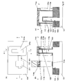
- the gate insulating film 120 is formed around the columnar semi-silicon layer 109 and the fifth insulating film 115a in the region where the second dummy gate 113a and the first dummy gate 106a exist.
- An inner region is formed on the inner side of the fifth insulating film 115b where the first dummy contact 113b is located.
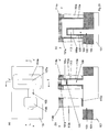
- a fifth resist 202 is formed to remove the gate insulating film 120 at the bottom of the region where the first dummy contact 113b was present.
- the gate insulating film 120 at the bottom of the region where the first dummy contact 113b was present is removed.
- the gate insulating film 120 is separated to form gate insulating films 120a and 120b.
- the gate insulating film 120b remains inside the fifth insulating film 115b, which is the region where the first dummy contact 113b was present.
- the gate insulating film 120 may be removed using isotropic etching. Therefore, it suffices to perform etching for the thickness of the gate insulating film, and a step of forming a deep contact hole is not necessary.
- the fifth resist 202 is removed.
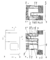
- a metal 121 is deposited.
- the metal 121 is etched back to expose the upper portion of the columnar silicon layer 109.
- a gate electrode 121 a is formed around the columnar silicon layer 109.
- the gate wiring 121b is formed.
- the first contact 121c is formed.
- the gate electrode 121a and the gate wiring 121b are insulated from the columnar silicon layer 109 and the fin-shaped silicon layer 103 by the gate insulating film 120 formed around and at the bottom of the gate electrode 121a and the gate wiring 121b. Can do.
- a contact stopper film is deposited, an interlayer insulating film is deposited, and chemical mechanical polishing is performed, and the second dummy gate, the first dummy gate, and the upper portion of the first dummy contact.
- the fifth dummy region is the region where the second dummy gate and the first dummy gate are located, the periphery of the columnar semiconductor layer, the inside of the fifth insulating film, and the first dummy contact.
- a second interlayer insulating film 122 is deposited.
- the second interlayer insulating film 122 is flattened to expose the first diffusion layer 112 on the columnar silicon layer 109.
- the second interlayer insulating film 122 is separated to form second interlayer insulating films 122a and 122b.
- a sixth resist 123 for forming contact holes is formed.
- contact holes 124 and 125 are formed by etching the second interlayer insulating films 122a and 122b.
- a metal 128 is deposited to form second contacts 129 and 131.
- seventh resists 132, 133, and 134 are formed to form metal wiring.
- the metal 128 is etched to form metal wirings 128a, 128b, and 128c.
- the seventh resists 132, 133, and 134 are removed.
- SGT is a gate last process in which the fin-like semiconductor layer, the columnar semiconductor layer, the gate electrode and the gate wiring are formed by self-alignment, and the dummy gate and the dummy contact are formed at the same time has been shown.
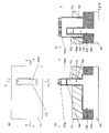
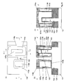
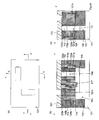
- FIG. 1 shows the structure of a semiconductor device obtained by the above manufacturing method.
- the areas of the upper surfaces of the gate electrode 121a and the gate wiring 121b are larger than the areas of the lower surfaces of the gate electrode 121a and the gate wiring 121b.
- the gate electrode 121a and the gate wiring 121b are insulated from the columnar silicon layer 109 and the fin-shaped silicon layer 103 by the gate insulating film 120 formed around and at the bottom of the gate electrode 121a and the gate wiring 121b. can do.
Landscapes
- Insulated Gate Type Field-Effect Transistor (AREA)
- Electrodes Of Semiconductors (AREA)
Abstract
フィン状半導体層、柱状半導体層、ゲート電極とゲート配線を自己整合で形成し、ダミーゲートとダミーコンタクトを同時に形成するゲートラストプロセスであるSGTの製造方法とその結果得られるSGTの構造を提供する。半導体基板上のフィン状半導体層の周囲に第1の絶縁膜を形成する第1工程と、第2の絶縁膜を形成し、第1のポリシリコンを堆積し平坦化し、第3の絶縁膜を形成し、第2のレジストを形成し、柱状半導体層と第1のダミーゲートと第1のハードマスクとを形成する第2工程と、第4の絶縁膜を形成し、第2のポリシリコンを堆積し平坦化し、エッチバックし、第6の絶縁膜を堆積し、第4のレジストを形成し、第2のハードマスクを形成し、第3のハードマスクを形成し、第2のダミーゲートを形成し、フィン状半導体層上に第1のダミーコンタクトを形成する第3工程とにより、課題を解決する。
Description
本発明は半導体装置の製造方法、及び、半導体装置に関する。
半導体集積回路、特にMOSトランジスタを用いた集積回路は、高集積化の一途を辿っている。この高集積化に伴って、その中で用いられているMOSトランジスタはナノ領域まで微細化が進んでいる。このようなMOSトランジスタの微細化が進むと、リーク電流の抑制が困難であり、必要な電流量確保の要請から回路の占有面積をなかなか小さくできない、といった問題があった。このような問題を解決するために、基板に対してソース、ゲート、ドレインが垂直方向に配置され、ゲート電極が柱状半導体層を取り囲む構造のSurrounding Gate Transistor(以下、「SGT」という。)が提案されている(例えば、特許文献1、特許文献2、特許文献3を参照)。
従来のSGTの製造方法では、シリコン柱を描画するためのマスクを用いて窒化膜ハードマスクが柱状に形成されたシリコン柱を形成し、平面状シリコン層を描画するためのマスクを用いてシリコン柱底部に平面状シリコン層を形成し、ゲート配線を描画するためのマスクを用いてゲート配線を形成している(例えば特許文献4を参照)。
すなわち、3つのマスクを用いてシリコン柱、平面状シリコン層、ゲート配線を形成している。
すなわち、3つのマスクを用いてシリコン柱、平面状シリコン層、ゲート配線を形成している。
また、従来のSGTの製造方法では、平面状シリコン層の上部と金属配線とを接続するために、深いコンタクト孔を形成している(例えば特許文献4を参照)。素子の微細化に伴い、コンタクト孔のアスペクト比(深さ/開口)は増大する。アスペクト比の増加と共にエッチング速度が低下する。また、パターンの微細化に伴い、レジストの膜厚は薄くなる。レジストの膜厚が薄くなると、エッチング中にレジストもエッチングされるため、深いコンタクト孔を形成することが難しくなる。
また、従来のMOSトランジスタにおいて、メタルゲートプロセスと高温プロセスを両立させるために、高温プロセス後にメタルゲートを作成するメタルゲートラストプロセスが実際の製品で用いられている(非特許文献1)。ポリシリコンでゲートを作成し、その後、層間絶縁膜を堆積後、化学機械研磨によりポリシリコンゲートを露出し、ポリシリコンゲートをエッチング後、メタルを堆積している。そのためSGTにおいてもメタルゲートプロセスと高温プロセスを両立させるために、高温プロセス後にメタルゲートを作成するメタルゲートラストプロセスを用いる必要がある。
また、メタルを埋め込む際、孔の下部より孔の上部が狭いと、孔の上部が先に埋まり、空孔が発生する。
また、ゲート配線と基板間の寄生容量を低減するために、従来のMOSトランジスタでは、第1の絶縁膜を用いている。例えばFINFET(非特許文献2)では、1つのフィン状半導体層の周囲に第1の絶縁膜を形成し、第1の絶縁膜をエッチバックし、フィン状半導体層を露出し、ゲート配線と基板間の寄生容量を低減している。そのためSGTにおいてもゲート配線と基板間の寄生容量を低減するために第1の絶縁膜を用いる必要がある。SGTではフィン状半導体層に加えて、柱状半導体層があるため、柱状半導体層を形成するための工夫が必要である。
IEDM2007 K.Mistry et.al, pp 247-250
IEDM2010 CC.Wu, et. al, 27.1.1-27.1.4.
そこで、フィン状半導体層、柱状半導体層、ゲート電極とゲート配線を自己整合で形成し、ダミーゲートとダミーコンタクトを同時に形成するゲートラストプロセスであるSGTの製造方法とその結果得られるSGTの構造を提供することを目的とする。
本発明の半導体装置の製造方法は、半導体基板上にフィン状半導体層を形成し、前記フィン状半導体層の周囲に第1の絶縁膜を形成する第1工程と、前記第1工程の後、前記フィン状半導体層の周囲に第2の絶縁膜を形成し、前記第2の絶縁膜の上に第1のポリシリコンを堆積し平坦化し、前記第1のポリシリコン上に第3の絶縁膜を形成し、ゲート配線と柱状半導体層を形成するための第2のレジストを、前記フィン状半導体層の方向に対して垂直の方向に形成し、前記第3の絶縁膜と前記第1のポリシリコンと前記第2の絶縁膜と前記フィン状半導体層をエッチングすることにより、柱状半導体層と前記第1のポリシリコンによる第1のダミーゲートと前記第3の絶縁膜による第1のハードマスクとを形成する第2工程と、前記第2工程の後、前記柱状半導体層と前記第1のダミーゲートの周囲に第4の絶縁膜を形成し、前記第4の絶縁膜の周囲に第2のポリシリコンを堆積し平坦化し、エッチバックし、前記第1のハードマスクを露出し、第6の絶縁膜を堆積し、第1のダミーコンタクトを形成するための第4のレジストを形成し、前記第6の絶縁膜をエッチングすることにより、前記第1のハードマスクの側壁に、第2のハードマスクを形成し、前記フィン状半導体層上に前記第1のダミーコンタクトを形成するための第3のハードマスクを形成し、前記第2のポリシリコンをエッチングすることにより、前記第1のダミーゲートと前記柱状半導体層の側壁に残存させ、第2のダミーゲートを形成し、前記フィン状半導体層上に前記第1のダミーコンタクトを形成する第3工程を有することを特徴とする。
また、前記第2のダミーゲートの上面の面積は、前記第2のダミーゲートの下面の面積より大きいことを特徴とする。
また、前記柱状半導体層と前記第1のダミーゲートの周囲に第4の絶縁膜を形成後、第3のレジストを形成し、エッチバックを行い、前記柱状半導体層上部を露出し、前記柱状半導体層上部に第1の拡散層を形成することを特徴とする。
また、前記第2のダミーゲートと前記第1のダミーコンタクトの周囲に、第5の絶縁膜を形成し、エッチングをし、サイドウォール状に残存させ、前記第5の絶縁膜からなるサイドウォールを形成し、前記フィン状半導体層上部と前記柱状半導体層下部に第2の拡散層を形成し、前記第2の拡散層上に金属と半導体の化合物を形成する第4工程を有することを特徴とする。
また、前記第4工程の後、コンタクトストッパ膜を堆積し、層間絶縁膜を堆積し化学機械研磨し、前記第2のダミーゲートと前記第1のダミーゲートと前記第1のダミーコンタクトの上部を露出し、前記第2のダミーゲートと前記第1のダミーゲートと前記第1のダミーコンタクトを除去し、前記第2の絶縁膜と前記第4の絶縁膜を除去し、ゲート絶縁膜を前記第2のダミーゲートと前記第1のダミーゲートがあった領域である前記柱状半導体層の周囲と前記第5の絶縁膜の内側と前記第1のダミーコンタクトがあった領域である前記第5の絶縁膜の内側に形成し、前記第1のダミーコンタクトがあった領域の底部の前記ゲート絶縁膜を除去するための第5のレジストを形成し、前記第1のダミーコンタクトがあった領域の底部の前記ゲート絶縁膜を除去し、金属を堆積し、エッチバックを行い、ゲート電極及びゲート配線と第1のコンタクトを形成する第5工程を有することを特徴とする。
また、本発明の半導体装置は、半導体基板上に形成されたフィン状半導体層と、前記フィン状半導体層の周囲に形成された第1の絶縁膜と、前記フィン状半導体層上に形成された第1のコンタクトと、前記第1のコンタクトの周囲に形成されたゲート絶縁膜と、を有することを特徴とする。
また、前記第1のコンタクトの上面の面積は前記第1のコンタクトの下面の面積より大きいことを特徴とする。
また、前記フィン状半導体層上に形成された柱状半導体層と、前記柱状半導体層の周囲に形成されたゲート絶縁膜と、前記ゲート絶縁膜の周囲に形成された金属からなるゲート電極と、前記ゲート電極に接続された前記フィン状半導体層に直交する方向に延在する金属からなるゲート配線と、前記柱状半導体層の上部に形成された第1の拡散層と、前記フィン状半導体層の上部と前記柱状半導体層の下部に形成された第2の拡散層と、を有し、前記ゲート電極と前記ゲート配線の上面の面積は前記ゲート電極と前記ゲート配線の下面の面積より大きいことを特徴とする。
また、前記ゲート電極と前記ゲート配線の周囲と底部に形成された前記ゲート絶縁膜とをさらに有することを特徴とする。
本発明によれば、フィン状半導体層、柱状半導体層、ゲート電極とゲート配線を自己整合で形成し、ダミーゲートとダミーコンタクトを同時に形成するゲートラストプロセスであるSGTの製造方法とその結果得られるSGTの構造を提供することができる。
半導体基板上にフィン状半導体層を形成し、前記フィン状半導体層の周囲に第1の絶縁膜を形成する第1工程と、前記第1工程の後、前記フィン状半導体層の周囲に第2の絶縁膜を形成し、前記第2の絶縁膜の上に第1のポリシリコンを堆積し平坦化し、前記第1のポリシリコン上に第3の絶縁膜を形成し、ゲート配線と柱状半導体層を形成するための第2のレジストを、前記フィン状半導体層の方向に対して垂直の方向に形成し、前記第3の絶縁膜と前記第1のポリシリコンと前記第2の絶縁膜と前記フィン状半導体層をエッチングすることにより、柱状半導体層と前記第1のポリシリコンによる第1のダミーゲートと前記第3の絶縁膜による第1のハードマスクとを形成する第2工程と、前記第2工程の後、前記柱状半導体層と前記第1のダミーゲートの周囲に第4の絶縁膜を形成し、前記第4の絶縁膜の周囲に第2のポリシリコンを堆積し平坦化し、エッチバックし、前記第1のハードマスクを露出し、第6の絶縁膜を堆積し、第1のダミーコンタクトを形成するための第4のレジストを形成し、前記第6の絶縁膜をエッチングすることにより、前記第1のハードマスクの側壁に、第2のハードマスクを形成し、前記フィン状半導体層上に前記第1のダミーコンタクトを形成するための第3のハードマスクを形成し、前記第2のポリシリコンをエッチングすることにより、前記第1のダミーゲートと前記柱状半導体層の側壁に残存させ、第2のダミーゲートを形成し、前記フィン状半導体層上に前記第1のダミーコンタクトを形成する第3工程を有することを特徴とすることにより、フィン状半導体層、柱状半導体層、ゲート電極とゲート配線を自己整合で形成することができ、工程数を削減することができる。
第2のダミーゲートと同時に第1のダミーコンタクトを形成し、後に、コンタクトストッパ膜を堆積し、層間絶縁膜を堆積し化学機械研磨し、前記第2のダミーゲートと前記第1のダミーゲートと前記第1のダミーコンタクトの上部を露出し、前記第2のダミーゲートと前記第1のダミーゲートと前記第1のダミーコンタクトを除去し、前記第2の絶縁膜と前記第4の絶縁膜を除去し、ゲート絶縁膜を前記第2のダミーゲートと前記第1のダミーゲートがあった領域である前記柱状半導体層の周囲と前記第5の絶縁膜の内側と前記第1のダミーコンタクトがあった領域である前記第5の絶縁膜の内側に形成し、前記第1のダミーコンタクトがあった領域の底部の前記ゲート絶縁膜を除去するための第5のレジストを形成し、前記第1のダミーコンタクトがあった領域の底部の前記ゲート絶縁膜を除去し、金属を堆積し、エッチバックを行うことにより、ゲート電極及びゲート配線と第1のコンタクトを形成することができる。従って、ゲート絶縁膜の膜厚分エッチングすればよく、深いコンタクト孔を形成する工程が不要となる。
また、前記第1のダミーコンタクトがあった領域の底部の前記ゲート絶縁膜を除去したため、前記第1のダミーコンタクトがあった領域である前記第5の絶縁膜の内側にゲート絶縁膜が残存する構造となる。ゲート絶縁膜は、原子層堆積により形成された絶縁性の高い膜であるため、第1のコンタクトと周囲の構造間とをより絶縁することができる。
また、第1と第2のハードマスクにより、第1と第2のダミーゲート上に金属と半導体の化合物が形成されることを防ぎ、フィン状半導体層上のみに金属と半導体の化合物を形成することができる。
また、第2のポリシリコンをエッチングする際、逆テーパエッチングを用いることにより、前記第2のダミーゲートの上面の面積は、前記第2のダミーゲートの下面の面積より大きくすることができ、ゲートのための金属を埋め込む際、空孔が形成されないようにすることができる。また、同時に前記第1のダミーコンタクトの上面の面積は、前記第1のダミーコンタクトの下面の面積より大きくすることができる。第1のコンタクトのための金属を埋め込む際、空孔が形成されないようにすることができる。
また、ポリシリコンで第1のダミーゲートと第2のダミーゲートを作成し、その後、層間絶縁膜を堆積後、化学機械研磨により第1のダミーゲートと第2のダミーゲートを露出し、ポリシリコンゲートをエッチング後、金属を堆積する従来のメタルゲートラストの製造方法を用いることができるため、メタルゲートSGTを容易に形成できる。
また、前記ゲート電極と前記ゲート配線の周囲と底部に形成された前記ゲート絶縁膜により、ゲート電極とゲート配線とは、柱状半導体層とフィン状半導体層とから絶縁をすることができる。
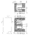
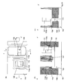
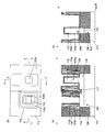
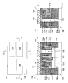
以下に、本発明の実施形態に係るSGTの構造を形成するための製造工程を、図2~図46を参照して説明する。
まず、半導体基板上にフィン状半導体層を形成し、前記フィン状半導体層の周囲に第1の絶縁膜を形成する第1工程を示す。本実施例では、シリコン基板としたが、基板はシリコン以外であっても半導体であればよい。
図2に示すように、シリコン基板101上にフィン状シリコン層を形成するための第1のレジスト102を形成する。
図3に示すように、シリコン基板101をエッチングし、フィン状シリコン層103を形成する。今回はレジストをマスクとしてフィン状シリコン層を形成したが、酸化膜や窒化膜といったハードマスクを用いてもよい。
図4に示すように、第1のレジスト102を除去する。
図5に示すように、フィン状シリコン層103の周囲に第1の絶縁膜104を堆積する。第1の絶縁膜として高密度プラズマによる酸化膜や低圧CVD(Chemical Vapor Deposition)による酸化膜を用いてもよい。
図6に示すように、第1の絶縁膜104をエッチバックし、フィン状シリコン層103の上部を露出する。ここまでは、非特許文献2のフィン状シリコン層の製法と同じである。
以上によりシリコン基板101上にフィン状シリコン層103を形成し、前記フィン状シリコン層103の周囲に第一の絶縁膜104を形成する第1工程が示された。
次に、前記フィン状半導体層の周囲に第2の絶縁膜を形成し、前記第2の絶縁膜の上に第1のポリシリコンを堆積し平坦化し、前記第1のポリシリコン上に第3の絶縁膜を形成し、ゲート配線と柱状半導体層を形成するための第2のレジストを、前記フィン状半導体層の方向に対して垂直の方向に形成し、前記第3の絶縁膜と前記第1のポリシリコンと前記第2の絶縁膜と前記フィン状半導体層をエッチングすることにより、柱状半導体層と前記第1のポリシリコンによる第1のダミーゲートと前記第3の絶縁膜による第1のハードマスクとを形成する第2工程を示す。
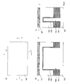
図7に示すように、前記フィン状シリコン層103の周囲に第2の絶縁膜105を形成する。第2の絶縁膜105は、酸化膜が好ましい。
図8に示すように、前記第2の絶縁膜105の上に第1のポリシリコン106を堆積し平坦化する。
図9に示すように、前記第1のポリシリコン106上に第3の絶縁膜107を形成する。第3の絶縁膜107は、窒化膜が好ましい。
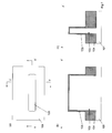
図10に示すように、ゲート配線と柱状シリコン層を形成するための第2のレジスト108を、前記フィン状シリコン層103の方向に対して垂直の方向に形成する。
図11に示すように、前記第3の絶縁膜107と前記第1のポリシリコン106と前記第2の絶縁膜105と前記フィン状シリコン層103をエッチングすることにより、柱状シリコン層109と前記第1のポリシリコンによる第1のダミーゲート106aと第3の絶縁膜による第1のハードマスク107aを形成する。
図12に示すように、第2のレジスト108を除去する。
以上により、前記フィン状半導体層の周囲に第2の絶縁膜を形成し、前記第2の絶縁膜の上に第1のポリシリコンを堆積し平坦化し、前記第1のポリシリコン上に第3の絶縁膜を形成し、ゲート配線と柱状半導体層を形成するための第2のレジストを、前記フィン状半導体層の方向に対して垂直の方向に形成し、前記第3の絶縁膜と前記第1のポリシリコンと前記第2の絶縁膜と前記フィン状半導体層をエッチングすることにより、柱状半導体層と前記第1のポリシリコンによる第1のダミーゲートと前記第3の絶縁膜による第1のハードマスクとを形成する第2工程が示された。
次に、前記第2工程の後、前記柱状半導体層と前記第1のダミーゲートの周囲に第4の絶縁膜を形成し、前記第4の絶縁膜の周囲に第2のポリシリコンを堆積し平坦化し、エッチバックし、前記第1のハードマスクを露出し、第6の絶縁膜を堆積し、第1のダミーコンタクトを形成するための第4のレジストを形成し、前記第6の絶縁膜をエッチングすることにより、前記第1のハードマスクの側壁に、第2のハードマスクを形成し、前記フィン状半導体層上に前記第1のダミーコンタクトを形成するための第3のハードマスクを形成し、前記第2のポリシリコンをエッチングすることにより、前記第1のダミーゲートと前記柱状半導体層の側壁に残存させ、第2のダミーゲートを形成し、前記フィン状半導体層上に前記第1のダミーコンタクトを形成する第3工程を示す。
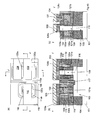
図13に示すように、前記柱状シリコン層109と前記第1のダミーゲート106aの周囲に第4の絶縁膜110を形成する。第4の絶縁膜110は、酸化膜が好ましい。
図14に示すように、第3のレジスト111を形成し、エッチバックを行い、前記柱状シリコン層109上部を露出する。
図15に示すように、不純物を導入し、前記柱状シリコン層109上部に第1の拡散層112を形成する。n型拡散層のときは、砒素やリンを導入することが好ましい。p型拡散層のときは、ボロンを導入することが好ましい。
図16に示すように、第3のレジスト111を除去する。
図17に示すように、前記第4の絶縁膜110の周囲に第2のポリシリコン113を堆積し平坦化する。
図18に示すように、第2のポリシリコン113をエッチバックし、前記第1のハードマスク107aを露出する。
図19に示すように、第6の絶縁膜114を堆積する。第6の絶縁膜114は窒化膜が好ましい。
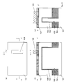
図20に示すように、第1のダミーコンタクトを形成するための第4のレジスト201を形成する。
図21に示すように、第6の絶縁膜114をエッチングすることにより、前記第1のハードマスク107aの側壁に、第2のハードマスク114aを形成し、前記フィン状シリコン層上に前記第1のダミーコンタクトを形成するための第3のハードマスク114bを形成する。
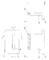
図22に示すように、前記第2のポリシリコン113をエッチングすることにより、前記第1のダミーゲート106aと前記柱状半導体層109の側壁に残存させ、第2のダミーゲート113aを形成し、前記フィン状シリコン層103上に第1のダミーコンタクト113bを形成する。また、第4の絶縁膜110は分離され、第4の絶縁膜110a、110bとなる。第2のポリシリコン113をエッチングする際、逆テーパエッチングを用いることにより、前記第2のダミーゲート113aの上面の面積は、前記第2のダミーゲート113aの下面の面積より大きくすることができ、ゲートのための金属を埋め込む際、空孔が形成されないようにすることができる。また、同時に前記第1のダミーコンタクト113bの上面の面積は、前記第1のダミーコンタクト113bの下面の面積より大きくすることができる。第1のコンタクトのための金属を埋め込む際、空孔が形成されないようにすることができる。
図23に示すように、第4のレジスト201を除去する。
以上により、前記第2工程の後、前記柱状半導体層と前記第1のダミーゲートの周囲に第4の絶縁膜を形成し、前記第4の絶縁膜の周囲に第2のポリシリコンを堆積し平坦化し、エッチバックし、前記第1のハードマスクを露出し、第6の絶縁膜を堆積し、第1のダミーコンタクトを形成するための第4のレジストを形成し、前記第6の絶縁膜をエッチングすることにより、前記第1のハードマスクの側壁に、第2のハードマスクを形成し、前記フィン状半導体層上に前記第1のダミーコンタクトを形成するための第3のハードマスクを形成し、前記第2のポリシリコンをエッチングすることにより、前記第1のダミーゲートと前記柱状半導体層の側壁に残存させ、第2のダミーゲートを形成し、前記フィン状半導体層上に前記第1のダミーコンタクトを形成する第3工程が示された。
次に、前記第2のダミーゲートと前記第1のダミーコンタクトの周囲に、第5の絶縁膜を形成し、エッチングをし、サイドウォール状に残存させ、前記第5の絶縁膜からなるサイドウォールを形成し、前記フィン状半導体層上部と前記柱状半導体層下部に第2の拡散層を形成し、前記第2の拡散層上に金属と半導体の化合物を形成する第4工程を示す。
図24に示すように、前記第2のダミーゲート113aと前記第1のダミーコンタクト113bの周囲に、第5の絶縁膜115を形成する。第5の絶縁膜115は、窒化膜が好ましい。
図25に示すように、第5の絶縁膜115をエッチングをし、サイドウォール状に残存させ、前記第5の絶縁膜からなるサイドウォール115a、115bを形成する。
図26に示すように、不純物を導入し、前記フィン状シリコン層103上部と前記柱状シリコン層109下部に第2の拡散層116を形成する。n型拡散層のときは、砒素やリンを導入することが好ましい。p型拡散層のときは、ボロンを導入することが好ましい。第5の絶縁膜115堆積前に不純物を導入してもよい。
図27に示すように、前記第2の拡散層116上に金属と半導体の化合物117を形成する。このとき、また、第1と第2のハードマスク107a、114aにより、第1と第2のダミーゲート106a、113a上に金属と半導体の化合物が形成されることを防ぎ、フィン状半導体層103上のみに金属と半導体の化合物を形成することができる。
以上により、前記第2のダミーゲートと前記第1のダミーコンタクトの周囲に、第5の絶縁膜を形成し、エッチングをし、サイドウォール状に残存させ、前記第5の絶縁膜からなるサイドウォールを形成し、前記フィン状半導体層上部と前記柱状半導体層下部に第2の拡散層を形成し、前記第2の拡散層上に金属と半導体の化合物を形成する第4工程が示された。
次に、前記第4工程の後、コンタクトストッパ膜を堆積し、層間絶縁膜を堆積し化学機械研磨し、前記第2のダミーゲートと前記第1のダミーゲートと前記第1のダミーコンタクトの上部を露出し、前記第2のダミーゲートと前記第1のダミーゲートと前記第1のダミーコンタクトを除去し、前記第2の絶縁膜と前記第4の絶縁膜を除去し、ゲート絶縁膜を前記第2のダミーゲートと前記第1のダミーゲートがあった領域である前記柱状半導体層の周囲と前記第5の絶縁膜の内側と前記第1のダミーコンタクトがあった領域である前記第5の絶縁膜の内側に形成し、前記第1のダミーコンタクトがあった領域の底部の前記ゲート絶縁膜を除去するための第5のレジストを形成し、前記第1のダミーコンタクトがあった領域の底部の前記ゲート絶縁膜を除去し、金属を堆積し、エッチバックを行い、ゲート電極及びゲート配線と第1のコンタクトを形成する第5工程を示す。
図28に示すように、コンタクトストッパ膜118を堆積し、層間絶縁膜119を堆積する。コンタクトストッパ膜118として、窒化膜が好ましい。また、コンタクトストッパ膜118を堆積しなくてもよい。
図29に示すように、化学機械研磨し、前記第2のダミーゲート113aと前記第1のダミーゲート106aと第1のダミーコンタクト113bの上部を露出する。
図30に示すように、前記第2のダミーゲート113aと前記第1のダミーゲート106aと第1のダミーコンタクト113bを除去する。
図31に示すように、前記第2の絶縁膜105と前記第4の絶縁膜110a、110bを除去する。
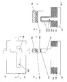
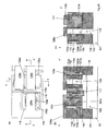
図32に示すように、ゲート絶縁膜120を前記第2のダミーゲート113aと前記第1のダミーゲート106aがあった領域である前記柱状半シリコン層109の周囲と前記第5の絶縁膜115aの内側と前記第1のダミーコンタクト113bがあった領域である前記第5の絶縁膜115bの内側に形成する。
図33に示すように、前記第1のダミーコンタクト113bがあった領域の底部の前記ゲート絶縁膜120を除去するための第5のレジスト202を形成する。
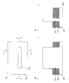
図34に示すように、前記第1のダミーコンタクト113bがあった領域の底部の前記ゲート絶縁膜120を除去する。ゲート絶縁膜120は分離され、ゲート絶縁膜120a、120bとなる。異方性エッチングを用いて除去したとき、前記第1のダミーコンタクト113bがあった領域である前記第5の絶縁膜115bの内側にゲート絶縁膜120bが残存する。等方性エッチングを用いてゲート絶縁膜120を除去してもよい。従って、ゲート絶縁膜の膜厚分エッチングすればよく、深いコンタクト孔を形成する工程が不要となる。
図35に示すように、第5のレジスト202を除去する。
図36に示すように、金属121を堆積する。
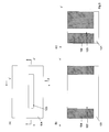
図37に示すように、金属121のエッチバックを行い、柱状シリコン層109上部を露出する。柱状シリコン層109の周囲にゲート電極121aが形成される。また、ゲート配線121bが形成される。また、第1のコンタクト121cが形成される。前記ゲート電極121aと前記ゲート配線121bの周囲と底部に形成された前記ゲート絶縁膜120により、ゲート電極121aとゲート配線121bとは、柱状シリコン層109とフィン状シリコン層103とから絶縁をすることができる。
以上により、前記第4工程の後、コンタクトストッパ膜を堆積し、層間絶縁膜を堆積し化学機械研磨し、前記第2のダミーゲートと前記第1のダミーゲートと前記第1のダミーコンタクトの上部を露出し、前記第2のダミーゲートと前記第1のダミーゲートと前記第1のダミーコンタクトを除去し、前記第2の絶縁膜と前記第4の絶縁膜を除去し、ゲート絶縁膜を前記第2のダミーゲートと前記第1のダミーゲートがあった領域である前記柱状半導体層の周囲と前記第5の絶縁膜の内側と前記第1のダミーコンタクトがあった領域である前記第5の絶縁膜の内側に形成し、前記第1のダミーコンタクトがあった領域の底部の前記ゲート絶縁膜を除去するための第5のレジストを形成し、前記第1のダミーコンタクトがあった領域の底部の前記ゲート絶縁膜を除去し、金属を堆積し、エッチバックを行い、ゲート電極及びゲート配線と第1のコンタクトを形成する第5工程が示された。
図38に示すように、第2の層間絶縁膜122を堆積する。
図39に示すように、第2の層間絶縁膜122を平坦化し、柱状シリコン層109上部の第1の拡散層112を露出する。第2の層間絶縁膜122は分離され、第2の層間絶縁膜122a、122bとなる。
図40に示すように、コンタクト孔を形成するための第6のレジスト123を形成する。
図41に示すように、第2の層間絶縁膜122a、122bをエッチングすることにより、コンタクト孔124、125を形成する。
図42に示すように、第6のレジスト123を除去する。
図43に示すように、金属128を堆積し、第2のコンタクト129、131を形成する。
図44に示すように、金属配線を形成するため第7のレジスト132、133、134を形成する。
図45に示すように、金属128をエッチングし、金属配線128a、128b、128cを形成する。
図46に示すように、第7のレジスト132、133、134を除去する。
以上により、フィン状半導体層、柱状半導体層、ゲート電極とゲート配線を自己整合で形成し、ダミーゲートとダミーコンタクトを同時に形成するゲートラストプロセスであるSGTの製造方法が示された。
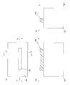
上記製造方法によって得られる半導体装置の構造を図1に示す。
シリコン基板101上に形成されたフィン状シリコン層103と、前記フィン状シリコン層103の周囲に形成された第1の絶縁膜104と、前記フィン状シリコン層103上に形成された第1のコンタクト121cと、前記第1のコンタクト121cの周囲に形成されたゲート絶縁膜120bと、を有する。前記第1のダミーコンタクト113bがあった領域の底部の前記ゲート絶縁膜120を除去したため、前記第1のダミーコンタクト113bがあった領域である前記第5の絶縁膜115bの内側にゲート絶縁膜120bが残存する構造となる。ゲート絶縁膜120は、原子層堆積といった絶縁性の高い膜であるため、第1のコンタクト121cと周囲の構造間とをより絶縁することができる。
前記フィン状シリコン層103上に形成された柱状シリコン層109と、前記柱状シリコン層109の周囲に形成されたゲート絶縁膜120aと、前記ゲート絶縁膜120aの周囲に形成された金属からなるゲート電極121aと、前記ゲート電極121aに接続された前記フィン状シリコン層103に直交する方向に延在する金属からなるゲート配線121bと、前記柱状シリコン層109の上部に形成された第1の拡散層112と、前記フィン状シリコン層103の上部と前記柱状シリコン層109の下部に形成された第2の拡散層116と、を有する。前記ゲート電極121aと前記ゲート配線121bの上面の面積は前記ゲート電極121aと前記ゲート配線121bの下面の面積より大きい。
セルフアラインで形成されるので、柱状シリコン層109と、ゲート配線121bとの合わせずれをなくすことができる。
また、前記ゲート電極121aと前記ゲート配線121bの周囲と底部に形成された前記ゲート絶縁膜120により、ゲート電極121aとゲート配線121bとは、柱状シリコン層109とフィン状シリコン層103とから絶縁をすることができる。
なお、本発明は、本発明の広義の精神と範囲を逸脱することなく、様々な実施形態及び変形が可能とされるものである。また、上述した実施形態は、本発明の一実施例を説明するためのものであり、本発明の範囲を限定するものではない。
例えば、上記実施例において、p型(p+型を含む。)とn型(n+型を含む。)とをそれぞれ反対の導電型とした半導体装置の製造方法、及び、それにより得られる半導体装置も当然に本発明の技術的範囲に含まれる。
101.シリコン基板
102.第1のレジスト
103.フィン状シリコン層
104.第1の絶縁膜
105.第2の絶縁膜
106.第1のポリシリコン
106a.第1のダミーゲート
107.第3の絶縁膜
107a.第1のハードマスク
108.第2のレジスト
109.柱状シリコン層
110.第4の絶縁膜
110a.第4の絶縁膜
110b.第4の絶縁膜
111.第3のレジスト
112.第1の拡散層
113.第2のポリシリコン
113a.第2のダミーゲート
113b.第1のダミーコンタクト
114.第6の絶縁膜
114a.第2のハードマスク
114b.第3のハードマスク
115.第5の絶縁膜
115a.第5の絶縁膜からなるサイドウォール
115b.第5の絶縁膜からなるサイドウォール
116.第2の拡散層
117.金属と半導体の化合物
118.コンタクトストッパ膜
119.層間絶縁膜
120.ゲート絶縁膜
120a.ゲート絶縁膜
120b.ゲート絶縁膜
121.金属
121a.ゲート電極
121b.ゲート配線
121c.第1のコンタクト
122.第2の層間絶縁膜
122a.第2の層間絶縁膜
122b.第2の層間絶縁膜
123.第6のレジスト
124.コンタクト孔
125.コンタクト孔
128.金属
128a.金属配線
128b.金属配線
128c.金属配線
129.第2のコンタクト
131.第2のコンタクト
132.第7のレジスト
133.第7のレジスト
134.第7のレジスト
201.第4のレジスト
202.第5のレジスト
102.第1のレジスト
103.フィン状シリコン層
104.第1の絶縁膜
105.第2の絶縁膜
106.第1のポリシリコン
106a.第1のダミーゲート
107.第3の絶縁膜
107a.第1のハードマスク
108.第2のレジスト
109.柱状シリコン層
110.第4の絶縁膜
110a.第4の絶縁膜
110b.第4の絶縁膜
111.第3のレジスト
112.第1の拡散層
113.第2のポリシリコン
113a.第2のダミーゲート
113b.第1のダミーコンタクト
114.第6の絶縁膜
114a.第2のハードマスク
114b.第3のハードマスク
115.第5の絶縁膜
115a.第5の絶縁膜からなるサイドウォール
115b.第5の絶縁膜からなるサイドウォール
116.第2の拡散層
117.金属と半導体の化合物
118.コンタクトストッパ膜
119.層間絶縁膜
120.ゲート絶縁膜
120a.ゲート絶縁膜
120b.ゲート絶縁膜
121.金属
121a.ゲート電極
121b.ゲート配線
121c.第1のコンタクト
122.第2の層間絶縁膜
122a.第2の層間絶縁膜
122b.第2の層間絶縁膜
123.第6のレジスト
124.コンタクト孔
125.コンタクト孔
128.金属
128a.金属配線
128b.金属配線
128c.金属配線
129.第2のコンタクト
131.第2のコンタクト
132.第7のレジスト
133.第7のレジスト
134.第7のレジスト
201.第4のレジスト
202.第5のレジスト
Claims (9)
- 半導体基板上にフィン状半導体層を形成し、前記フィン状半導体層の周囲に第1の絶縁膜を形成する第1工程と、
前記第1工程の後、前記フィン状半導体層の周囲に第2の絶縁膜を形成し、前記第2の絶縁膜の上に第1のポリシリコンを堆積し平坦化し、前記第1のポリシリコン上に第3の絶縁膜を形成し、ゲート配線と柱状半導体層を形成するための第2のレジストを、前記フィン状半導体層の方向に対して垂直の方向に形成し、前記第3の絶縁膜と前記第1のポリシリコンと前記第2の絶縁膜と前記フィン状半導体層をエッチングすることにより、柱状半導体層と前記第1のポリシリコンによる第1のダミーゲートと前記第3の絶縁膜による第1のハードマスクとを形成する第2工程と、
前記第2工程の後、前記柱状半導体層と前記第1のダミーゲートの周囲に第4の絶縁膜を形成し、前記第4の絶縁膜の周囲に第2のポリシリコンを堆積し平坦化し、エッチバックし、前記第1のハードマスクを露出し、第6の絶縁膜を堆積し、第1のダミーコンタクトを形成するための第4のレジストを形成し、前記第6の絶縁膜をエッチングすることにより、前記第1のハードマスクの側壁に、第2のハードマスクを形成し、前記フィン状半導体層上に前記第1のダミーコンタクトを形成するための第3のハードマスクを形成し、前記第2のポリシリコンをエッチングすることにより、前記第1のダミーゲートと前記柱状半導体層の側壁に残存させ、第2のダミーゲートを形成し、前記フィン状半導体層上に前記第1のダミーコンタクトを形成する第3工程と、
を有することを特徴とする半導体装置の製造方法。 - 前記第2のダミーゲートの上面の面積は、前記第2のダミーゲートの下面の面積より大きいことを特徴とする請求項1に記載の半導体装置。
- 前記柱状半導体層と前記第1のダミーゲートの周囲に第4の絶縁膜を形成後、第3のレジストを形成し、エッチバックを行い、前記柱状半導体層上部を露出し、前記柱状半導体層上部に第1の拡散層を形成することを特徴とする請求項1に記載の半導体装置の製造方法。
- 前記第2のダミーゲートと前記第1のダミーコンタクトの周囲に、第5の絶縁膜を形成し、エッチングをし、サイドウォール状に残存させ、前記第5の絶縁膜からなるサイドウォールを形成し、前記フィン状半導体層上部と前記柱状半導体層下部に第2の拡散層を形成し、前記第2の拡散層上に金属と半導体の化合物を形成する第4工程を有することを特徴とする請求項1に記載の半導体装置の製造方法。
- 前記第4工程の後、コンタクトストッパ膜を堆積し、層間絶縁膜を堆積し化学機械研磨し、前記第2のダミーゲートと前記第1のダミーゲートと前記第1のダミーコンタクトの上部を露出し、前記第2のダミーゲートと前記第1のダミーゲートと前記第1のダミーコンタクトを除去し、前記第2の絶縁膜と前記第4の絶縁膜を除去し、ゲート絶縁膜を前記第2のダミーゲートと前記第1のダミーゲートがあった領域である前記柱状半導体層の周囲と前記第5の絶縁膜の内側と前記第1のダミーコンタクトがあった領域である前記第5の絶縁膜の内側に形成し、前記第1のダミーコンタクトがあった領域の底部の前記ゲート絶縁膜を除去するための第5のレジストを形成し、前記第1のダミーコンタクトがあった領域の底部の前記ゲート絶縁膜を除去し、金属を堆積し、エッチバックを行い、ゲート電極及びゲート配線と第1のコンタクトを形成する第5工程を有することを特徴とする請求項5に記載の半導体装置の製造方法。
- 半導体基板上に形成されたフィン状半導体層と、
前記フィン状半導体層の周囲に形成された第1の絶縁膜と、
前記フィン状半導体層上に形成された第1のコンタクトと、
前記第1のコンタクトの周囲に形成されたゲート絶縁膜と、
を有することを特徴とする半導体装置。 - 前記第1のコンタクトの上面の面積は前記第1のコンタクトの下面の面積より大きいことを特徴とする請求項6に記載の半導体装置。
- 前記フィン状半導体層上に形成された柱状半導体層と、
前記柱状半導体層の周囲に形成されたゲート絶縁膜と、
前記ゲート絶縁膜の周囲に形成された金属からなるゲート電極と、
前記ゲート電極に接続された前記フィン状半導体層に直交する方向に延在する金属からなるゲート配線と、
前記柱状半導体層の上部に形成された第1の拡散層と、
前記フィン状半導体層の上部と前記柱状半導体層の下部に形成された第2の拡散層と、
を有し、
前記ゲート電極と前記ゲート配線の上面の面積は前記ゲート電極と前記ゲート配線の下面の面積より大きいことを特徴とする請求項6に記載の半導体装置。 - 前記ゲート電極と前記ゲート配線の周囲と底部に形成された前記ゲート絶縁膜とをさらに有することを特徴とする請求項8に記載の半導体装置。
Priority Applications (4)
| Application Number | Priority Date | Filing Date | Title |
|---|---|---|---|
| JP2015520742A JP5838530B1 (ja) | 2014-03-05 | 2014-03-05 | 半導体装置の製造方法、及び、半導体装置 |
| PCT/JP2014/055667 WO2015132912A1 (ja) | 2014-03-05 | 2014-03-05 | 半導体装置の製造方法、及び、半導体装置 |
| US15/191,711 US9865741B2 (en) | 2014-03-05 | 2016-06-24 | Method for producing semiconductor device and semiconductor device |
| US15/824,017 US9960277B2 (en) | 2014-03-05 | 2017-11-28 | Method for producing semiconductor device |
Applications Claiming Priority (1)
| Application Number | Priority Date | Filing Date | Title |
|---|---|---|---|
| PCT/JP2014/055667 WO2015132912A1 (ja) | 2014-03-05 | 2014-03-05 | 半導体装置の製造方法、及び、半導体装置 |
Related Child Applications (1)
| Application Number | Title | Priority Date | Filing Date |
|---|---|---|---|
| US15/191,711 Continuation US9865741B2 (en) | 2014-03-05 | 2016-06-24 | Method for producing semiconductor device and semiconductor device |
Publications (1)
| Publication Number | Publication Date |
|---|---|
| WO2015132912A1 true WO2015132912A1 (ja) | 2015-09-11 |
Family
ID=54054749
Family Applications (1)
| Application Number | Title | Priority Date | Filing Date |
|---|---|---|---|
| PCT/JP2014/055667 Ceased WO2015132912A1 (ja) | 2014-03-05 | 2014-03-05 | 半導体装置の製造方法、及び、半導体装置 |
Country Status (3)
| Country | Link |
|---|---|
| US (2) | US9865741B2 (ja) |
| JP (1) | JP5838530B1 (ja) |
| WO (1) | WO2015132912A1 (ja) |
Cited By (2)
| Publication number | Priority date | Publication date | Assignee | Title |
|---|---|---|---|---|
| US20160308065A1 (en) * | 2014-03-05 | 2016-10-20 | Unisantis Electronics Singapore Pte. Ltd. | Method for producing semiconductor device and semiconductor device |
| JP2020043356A (ja) * | 2016-03-24 | 2020-03-19 | 東京エレクトロン株式会社 | 半導体装置の製造方法 |
Families Citing this family (3)
| Publication number | Priority date | Publication date | Assignee | Title |
|---|---|---|---|---|
| WO2015125204A1 (ja) * | 2014-02-18 | 2015-08-27 | ユニサンティス エレクトロニクス シンガポール プライベート リミテッド | 半導体装置の製造方法、及び、半導体装置 |
| US9620628B1 (en) * | 2016-07-07 | 2017-04-11 | Taiwan Semiconductor Manufacturing Co., Ltd. | Methods of forming contact feature |
| US11088033B2 (en) * | 2016-09-08 | 2021-08-10 | International Business Machines Corporation | Low resistance source-drain contacts using high temperature silicides |
Citations (4)
| Publication number | Priority date | Publication date | Assignee | Title |
|---|---|---|---|---|
| JP2009070975A (ja) * | 2007-09-12 | 2009-04-02 | Elpida Memory Inc | 半導体装置およびその製造方法 |
| JP2011040682A (ja) * | 2009-08-18 | 2011-02-24 | Unisantis Electronics Japan Ltd | 半導体装置とその製造方法 |
| JP2013239622A (ja) * | 2012-05-16 | 2013-11-28 | Toshiba Corp | 不揮発性半導体記憶装置及びその製造方法 |
| WO2014024266A1 (ja) * | 2012-08-08 | 2014-02-13 | ユニサンティス エレクトロニクス シンガポール プライベート リミテッド | 半導体装置の製造方法、及び、半導体装置 |
Family Cites Families (29)
| Publication number | Priority date | Publication date | Assignee | Title |
|---|---|---|---|---|
| JP3057661B2 (ja) | 1988-09-06 | 2000-07-04 | 株式会社東芝 | 半導体装置 |
| US5258635A (en) | 1988-09-06 | 1993-11-02 | Kabushiki Kaisha Toshiba | MOS-type semiconductor integrated circuit device |
| JP2703970B2 (ja) | 1989-01-17 | 1998-01-26 | 株式会社東芝 | Mos型半導体装置 |
| JP2950558B2 (ja) | 1989-11-01 | 1999-09-20 | 株式会社東芝 | 半導体装置 |
| KR101225641B1 (ko) * | 2006-12-27 | 2013-01-24 | 삼성전자주식회사 | 반도체 소자 및 그 제조 방법 |
| JP4316658B2 (ja) | 2008-01-29 | 2009-08-19 | 日本ユニサンティスエレクトロニクス株式会社 | 半導体装置の製造方法 |
| US8476132B2 (en) * | 2008-01-29 | 2013-07-02 | Unisantis Electronics Singapore Pte Ltd. | Production method for semiconductor device |
| JP5317343B2 (ja) * | 2009-04-28 | 2013-10-16 | ユニサンティス エレクトロニクス シンガポール プライベート リミテッド | 半導体装置及びその製造方法 |
| US8188537B2 (en) * | 2008-01-29 | 2012-05-29 | Unisantis Electronics Singapore Pte Ltd. | Semiconductor device and production method therefor |
| US8212298B2 (en) * | 2008-01-29 | 2012-07-03 | Unisantis Electronics Singapore Pte Ltd. | Semiconductor storage device and methods of producing it |
| US8598650B2 (en) * | 2008-01-29 | 2013-12-03 | Unisantis Electronics Singapore Pte Ltd. | Semiconductor device and production method therefor |
| US8026141B2 (en) * | 2008-02-08 | 2011-09-27 | Unisantis Electronics (Japan) Ltd. | Method of producing semiconductor |
| US8211809B2 (en) * | 2008-09-02 | 2012-07-03 | Unisantis Electronics Singapore Pte Ltd. | Method of producing semiconductor device |
| JP4487221B1 (ja) * | 2009-04-17 | 2010-06-23 | 日本ユニサンティスエレクトロニクス株式会社 | 半導体装置 |
| JP4577592B2 (ja) * | 2009-04-20 | 2010-11-10 | 日本ユニサンティスエレクトロニクス株式会社 | 半導体装置の製造方法 |
| JP5031809B2 (ja) * | 2009-11-13 | 2012-09-26 | ユニサンティス エレクトロニクス シンガポール プライベート リミテッド | 半導体装置 |
| US8916478B2 (en) * | 2011-12-19 | 2014-12-23 | Unisantis Electronics Singapore Pte. Ltd. | Method for manufacturing semiconductor device and semiconductor device |
| US8697511B2 (en) * | 2012-05-18 | 2014-04-15 | Unisantis Electronics Singapore Pte. Ltd. | Method for producing semiconductor device and semiconductor device |
| US8877578B2 (en) * | 2012-05-18 | 2014-11-04 | Unisantis Electronics Singapore Pte. Ltd. | Method for producing semiconductor device and semiconductor device |
| JP5677643B1 (ja) * | 2013-08-08 | 2015-02-25 | ユニサンティス エレクトロニクス シンガポール プライベート リミテッドUnisantis Electronics Singapore Pte Ltd. | 半導体装置 |
| JP5688190B1 (ja) * | 2013-09-03 | 2015-03-25 | ユニサンティス エレクトロニクス シンガポール プライベート リミテッドUnisantis Electronics Singapore Pte Ltd. | 半導体装置 |
| WO2015033382A1 (ja) * | 2013-09-03 | 2015-03-12 | ユニサンティス エレクトロニクス シンガポール プライベート リミテッド | 半導体装置 |
| WO2015125204A1 (ja) * | 2014-02-18 | 2015-08-27 | ユニサンティス エレクトロニクス シンガポール プライベート リミテッド | 半導体装置の製造方法、及び、半導体装置 |
| JP5822326B1 (ja) * | 2014-02-18 | 2015-11-24 | ユニサンティス エレクトロニクス シンガポール プライベート リミテッドUnisantis Electronics Singapore Pte Ltd. | 半導体装置の製造方法、及び、半導体装置 |
| WO2015132913A1 (ja) * | 2014-03-05 | 2015-09-11 | ユニサンティス エレクトロニクス シンガポール プライベート リミテッド | 半導体装置の製造方法、及び、半導体装置 |
| JP5838530B1 (ja) * | 2014-03-05 | 2016-01-06 | ユニサンティス エレクトロニクス シンガポール プライベート リミテッドUnisantis Electronics Singapore Pte Ltd. | 半導体装置の製造方法、及び、半導体装置 |
| JP5833279B1 (ja) * | 2014-04-10 | 2015-12-16 | ユニサンティス エレクトロニクス シンガポール プライベート リミテッドUnisantis Electronics Singapore Pte Ltd. | 半導体装置 |
| WO2015189916A1 (ja) * | 2014-06-10 | 2015-12-17 | ユニサンティス エレクトロニクス シンガポール プライベート リミテッド | 柱状半導体メモリ装置及びその製造方法 |
| WO2016013087A1 (ja) * | 2014-07-24 | 2016-01-28 | ユニサンティス エレクトロニクス シンガポール プライベート リミテッド | 半導体装置の製造方法、及び、半導体装置 |
-
2014
- 2014-03-05 JP JP2015520742A patent/JP5838530B1/ja active Active
- 2014-03-05 WO PCT/JP2014/055667 patent/WO2015132912A1/ja not_active Ceased
-
2016
- 2016-06-24 US US15/191,711 patent/US9865741B2/en active Active
-
2017
- 2017-11-28 US US15/824,017 patent/US9960277B2/en active Active
Patent Citations (4)
| Publication number | Priority date | Publication date | Assignee | Title |
|---|---|---|---|---|
| JP2009070975A (ja) * | 2007-09-12 | 2009-04-02 | Elpida Memory Inc | 半導体装置およびその製造方法 |
| JP2011040682A (ja) * | 2009-08-18 | 2011-02-24 | Unisantis Electronics Japan Ltd | 半導体装置とその製造方法 |
| JP2013239622A (ja) * | 2012-05-16 | 2013-11-28 | Toshiba Corp | 不揮発性半導体記憶装置及びその製造方法 |
| WO2014024266A1 (ja) * | 2012-08-08 | 2014-02-13 | ユニサンティス エレクトロニクス シンガポール プライベート リミテッド | 半導体装置の製造方法、及び、半導体装置 |
Cited By (4)
| Publication number | Priority date | Publication date | Assignee | Title |
|---|---|---|---|---|
| US20160308065A1 (en) * | 2014-03-05 | 2016-10-20 | Unisantis Electronics Singapore Pte. Ltd. | Method for producing semiconductor device and semiconductor device |
| US9865741B2 (en) * | 2014-03-05 | 2018-01-09 | Unisantis Electronics Singapore Pte. Ltd. | Method for producing semiconductor device and semiconductor device |
| US9960277B2 (en) | 2014-03-05 | 2018-05-01 | Unisantis Electronics Singapore Pte. Ltd. | Method for producing semiconductor device |
| JP2020043356A (ja) * | 2016-03-24 | 2020-03-19 | 東京エレクトロン株式会社 | 半導体装置の製造方法 |
Also Published As
| Publication number | Publication date |
|---|---|
| US9865741B2 (en) | 2018-01-09 |
| US20180090623A1 (en) | 2018-03-29 |
| JPWO2015132912A1 (ja) | 2017-03-30 |
| US20160308065A1 (en) | 2016-10-20 |
| JP5838530B1 (ja) | 2016-01-06 |
| US9960277B2 (en) | 2018-05-01 |
Similar Documents
| Publication | Publication Date | Title |
|---|---|---|
| JP5822326B1 (ja) | 半導体装置の製造方法、及び、半導体装置 | |
| JP5731073B1 (ja) | 半導体装置の製造方法、及び、半導体装置 | |
| JP5759077B1 (ja) | 半導体装置の製造方法、及び、半導体装置 | |
| JP5779739B1 (ja) | 半導体装置の製造方法、及び、半導体装置 | |
| JP5838530B1 (ja) | 半導体装置の製造方法、及び、半導体装置 | |
| JP5838529B1 (ja) | 半導体装置の製造方法、及び、半導体装置 | |
| JP5775650B1 (ja) | 半導体装置の製造方法、及び、半導体装置 | |
| JP5680801B1 (ja) | 半導体装置の製造方法、及び、半導体装置 | |
| JP5872054B2 (ja) | 半導体装置の製造方法、及び、半導体装置 | |
| JP5740535B1 (ja) | 半導体装置の製造方法、及び、半導体装置 | |
| JP6154051B2 (ja) | 半導体装置の製造方法、及び、半導体装置 | |
| JP5989197B2 (ja) | 半導体装置の製造方法、及び、半導体装置 | |
| JP6121386B2 (ja) | 半導体装置の製造方法、及び、半導体装置 | |
| JP5861197B2 (ja) | 半導体装置の製造方法、及び、半導体装置 | |
| JP6033938B2 (ja) | 半導体装置の製造方法、及び、半導体装置 | |
| JP5977865B2 (ja) | 半導体装置の製造方法、及び、半導体装置 | |
| JP6080989B2 (ja) | 半導体装置の製造方法、及び、半導体装置 | |
| JP5869166B2 (ja) | 半導体装置の製造方法、及び、半導体装置 | |
| JP6174174B2 (ja) | 半導体装置の製造方法、及び、半導体装置 | |
| JP6200478B2 (ja) | 半導体装置の製造方法、及び、半導体装置 | |
| JP2015119196A (ja) | 半導体装置の製造方法及び半導体装置 | |
| JP2015159320A (ja) | 半導体装置の製造方法、及び、半導体装置 |
Legal Events
| Date | Code | Title | Description |
|---|---|---|---|
| ENP | Entry into the national phase |
Ref document number: 2015520742 Country of ref document: JP Kind code of ref document: A |
|
| 121 | Ep: the epo has been informed by wipo that ep was designated in this application |
Ref document number: 14884283 Country of ref document: EP Kind code of ref document: A1 |
|
| NENP | Non-entry into the national phase |
Ref country code: DE |
|
| 122 | Ep: pct application non-entry in european phase |
Ref document number: 14884283 Country of ref document: EP Kind code of ref document: A1 |