WO2015125855A1 - 鉛フリーはんだ合金、はんだ材料及び接合構造体 - Google Patents
鉛フリーはんだ合金、はんだ材料及び接合構造体 Download PDFInfo
- Publication number
- WO2015125855A1 WO2015125855A1 PCT/JP2015/054581 JP2015054581W WO2015125855A1 WO 2015125855 A1 WO2015125855 A1 WO 2015125855A1 JP 2015054581 W JP2015054581 W JP 2015054581W WO 2015125855 A1 WO2015125855 A1 WO 2015125855A1
- Authority
- WO
- WIPO (PCT)
- Prior art keywords
- mass
- solder alloy
- lead
- solder
- free solder
- Prior art date
Links
Images


Classifications
-
- B—PERFORMING OPERATIONS; TRANSPORTING
- B23—MACHINE TOOLS; METAL-WORKING NOT OTHERWISE PROVIDED FOR
- B23K—SOLDERING OR UNSOLDERING; WELDING; CLADDING OR PLATING BY SOLDERING OR WELDING; CUTTING BY APPLYING HEAT LOCALLY, e.g. FLAME CUTTING; WORKING BY LASER BEAM
- B23K35/00—Rods, electrodes, materials, or media, for use in soldering, welding, or cutting
- B23K35/22—Rods, electrodes, materials, or media, for use in soldering, welding, or cutting characterised by the composition or nature of the material
- B23K35/24—Selection of soldering or welding materials proper
- B23K35/26—Selection of soldering or welding materials proper with the principal constituent melting at less than 400 degrees C
- B23K35/262—Sn as the principal constituent
-
- B—PERFORMING OPERATIONS; TRANSPORTING
- B23—MACHINE TOOLS; METAL-WORKING NOT OTHERWISE PROVIDED FOR
- B23K—SOLDERING OR UNSOLDERING; WELDING; CLADDING OR PLATING BY SOLDERING OR WELDING; CUTTING BY APPLYING HEAT LOCALLY, e.g. FLAME CUTTING; WORKING BY LASER BEAM
- B23K35/00—Rods, electrodes, materials, or media, for use in soldering, welding, or cutting
- B23K35/02—Rods, electrodes, materials, or media, for use in soldering, welding, or cutting characterised by mechanical features, e.g. shape
- B23K35/0222—Rods, electrodes, materials, or media, for use in soldering, welding, or cutting characterised by mechanical features, e.g. shape for use in soldering, brazing
-
- B—PERFORMING OPERATIONS; TRANSPORTING
- B23—MACHINE TOOLS; METAL-WORKING NOT OTHERWISE PROVIDED FOR
- B23K—SOLDERING OR UNSOLDERING; WELDING; CLADDING OR PLATING BY SOLDERING OR WELDING; CUTTING BY APPLYING HEAT LOCALLY, e.g. FLAME CUTTING; WORKING BY LASER BEAM
- B23K35/00—Rods, electrodes, materials, or media, for use in soldering, welding, or cutting
- B23K35/22—Rods, electrodes, materials, or media, for use in soldering, welding, or cutting characterised by the composition or nature of the material
- B23K35/24—Selection of soldering or welding materials proper
- B23K35/26—Selection of soldering or welding materials proper with the principal constituent melting at less than 400 degrees C
-
- B—PERFORMING OPERATIONS; TRANSPORTING
- B23—MACHINE TOOLS; METAL-WORKING NOT OTHERWISE PROVIDED FOR
- B23K—SOLDERING OR UNSOLDERING; WELDING; CLADDING OR PLATING BY SOLDERING OR WELDING; CUTTING BY APPLYING HEAT LOCALLY, e.g. FLAME CUTTING; WORKING BY LASER BEAM
- B23K35/00—Rods, electrodes, materials, or media, for use in soldering, welding, or cutting
- B23K35/22—Rods, electrodes, materials, or media, for use in soldering, welding, or cutting characterised by the composition or nature of the material
- B23K35/36—Selection of non-metallic compositions, e.g. coatings, fluxes; Selection of soldering or welding materials, conjoint with selection of non-metallic compositions, both selections being of interest
-
- C—CHEMISTRY; METALLURGY
- C22—METALLURGY; FERROUS OR NON-FERROUS ALLOYS; TREATMENT OF ALLOYS OR NON-FERROUS METALS
- C22C—ALLOYS
- C22C13/00—Alloys based on tin
- C22C13/02—Alloys based on tin with antimony or bismuth as the next major constituent
-
- H—ELECTRICITY
- H01—ELECTRIC ELEMENTS
- H01L—SEMICONDUCTOR DEVICES NOT COVERED BY CLASS H10
- H01L24/00—Arrangements for connecting or disconnecting semiconductor or solid-state bodies; Methods or apparatus related thereto
- H01L24/01—Means for bonding being attached to, or being formed on, the surface to be connected, e.g. chip-to-package, die-attach, "first-level" interconnects; Manufacturing methods related thereto
- H01L24/10—Bump connectors ; Manufacturing methods related thereto
- H01L24/15—Structure, shape, material or disposition of the bump connectors after the connecting process
- H01L24/16—Structure, shape, material or disposition of the bump connectors after the connecting process of an individual bump connector
-
- H—ELECTRICITY
- H05—ELECTRIC TECHNIQUES NOT OTHERWISE PROVIDED FOR
- H05K—PRINTED CIRCUITS; CASINGS OR CONSTRUCTIONAL DETAILS OF ELECTRIC APPARATUS; MANUFACTURE OF ASSEMBLAGES OF ELECTRICAL COMPONENTS
- H05K3/00—Apparatus or processes for manufacturing printed circuits
- H05K3/30—Assembling printed circuits with electric components, e.g. with resistor
- H05K3/32—Assembling printed circuits with electric components, e.g. with resistor electrically connecting electric components or wires to printed circuits
- H05K3/34—Assembling printed circuits with electric components, e.g. with resistor electrically connecting electric components or wires to printed circuits by soldering
- H05K3/3457—Solder materials or compositions; Methods of application thereof
- H05K3/3463—Solder compositions in relation to features of the printed circuit board or the mounting process
-
- B—PERFORMING OPERATIONS; TRANSPORTING
- B23—MACHINE TOOLS; METAL-WORKING NOT OTHERWISE PROVIDED FOR
- B23K—SOLDERING OR UNSOLDERING; WELDING; CLADDING OR PLATING BY SOLDERING OR WELDING; CUTTING BY APPLYING HEAT LOCALLY, e.g. FLAME CUTTING; WORKING BY LASER BEAM
- B23K2101/00—Articles made by soldering, welding or cutting
- B23K2101/36—Electric or electronic devices
- B23K2101/40—Semiconductor devices
-
- H—ELECTRICITY
- H01—ELECTRIC ELEMENTS
- H01L—SEMICONDUCTOR DEVICES NOT COVERED BY CLASS H10
- H01L2224/00—Indexing scheme for arrangements for connecting or disconnecting semiconductor or solid-state bodies and methods related thereto as covered by H01L24/00
- H01L2224/01—Means for bonding being attached to, or being formed on, the surface to be connected, e.g. chip-to-package, die-attach, "first-level" interconnects; Manufacturing methods related thereto
- H01L2224/10—Bump connectors; Manufacturing methods related thereto
- H01L2224/12—Structure, shape, material or disposition of the bump connectors prior to the connecting process
- H01L2224/13—Structure, shape, material or disposition of the bump connectors prior to the connecting process of an individual bump connector
- H01L2224/13001—Core members of the bump connector
- H01L2224/13099—Material
- H01L2224/13198—Material with a principal constituent of the material being a combination of two or more materials in the form of a matrix with a filler, i.e. being a hybrid material, e.g. segmented structures, foams
- H01L2224/13298—Fillers
- H01L2224/13299—Base material
- H01L2224/133—Base material with a principal constituent of the material being a metal or a metalloid, e.g. boron [B], silicon [Si], germanium [Ge], arsenic [As], antimony [Sb], tellurium [Te] and polonium [Po], and alloys thereof
- H01L2224/13301—Base material with a principal constituent of the material being a metal or a metalloid, e.g. boron [B], silicon [Si], germanium [Ge], arsenic [As], antimony [Sb], tellurium [Te] and polonium [Po], and alloys thereof the principal constituent melting at a temperature of less than 400°C
- H01L2224/13311—Tin [Sn] as principal constituent
-
- H—ELECTRICITY
- H01—ELECTRIC ELEMENTS
- H01L—SEMICONDUCTOR DEVICES NOT COVERED BY CLASS H10
- H01L2224/00—Indexing scheme for arrangements for connecting or disconnecting semiconductor or solid-state bodies and methods related thereto as covered by H01L24/00
- H01L2224/01—Means for bonding being attached to, or being formed on, the surface to be connected, e.g. chip-to-package, die-attach, "first-level" interconnects; Manufacturing methods related thereto
- H01L2224/10—Bump connectors; Manufacturing methods related thereto
- H01L2224/12—Structure, shape, material or disposition of the bump connectors prior to the connecting process
- H01L2224/13—Structure, shape, material or disposition of the bump connectors prior to the connecting process of an individual bump connector
- H01L2224/1354—Coating
- H01L2224/13599—Material
- H01L2224/136—Material with a principal constituent of the material being a metal or a metalloid, e.g. boron [B], silicon [Si], germanium [Ge], arsenic [As], antimony [Sb], tellurium [Te] and polonium [Po], and alloys thereof
- H01L2224/13601—Material with a principal constituent of the material being a metal or a metalloid, e.g. boron [B], silicon [Si], germanium [Ge], arsenic [As], antimony [Sb], tellurium [Te] and polonium [Po], and alloys thereof the principal constituent melting at a temperature of less than 400°C
- H01L2224/13611—Tin [Sn] as principal constituent
-
- H—ELECTRICITY
- H01—ELECTRIC ELEMENTS
- H01L—SEMICONDUCTOR DEVICES NOT COVERED BY CLASS H10
- H01L2224/00—Indexing scheme for arrangements for connecting or disconnecting semiconductor or solid-state bodies and methods related thereto as covered by H01L24/00
- H01L2224/01—Means for bonding being attached to, or being formed on, the surface to be connected, e.g. chip-to-package, die-attach, "first-level" interconnects; Manufacturing methods related thereto
- H01L2224/10—Bump connectors; Manufacturing methods related thereto
- H01L2224/12—Structure, shape, material or disposition of the bump connectors prior to the connecting process
- H01L2224/13—Structure, shape, material or disposition of the bump connectors prior to the connecting process of an individual bump connector
- H01L2224/1354—Coating
- H01L2224/13599—Material
- H01L2224/136—Material with a principal constituent of the material being a metal or a metalloid, e.g. boron [B], silicon [Si], germanium [Ge], arsenic [As], antimony [Sb], tellurium [Te] and polonium [Po], and alloys thereof
- H01L2224/13617—Material with a principal constituent of the material being a metal or a metalloid, e.g. boron [B], silicon [Si], germanium [Ge], arsenic [As], antimony [Sb], tellurium [Te] and polonium [Po], and alloys thereof the principal constituent melting at a temperature of greater than or equal to 400°C and less than 950°C
- H01L2224/1362—Antimony [Sb] as principal constituent
-
- H—ELECTRICITY
- H01—ELECTRIC ELEMENTS
- H01L—SEMICONDUCTOR DEVICES NOT COVERED BY CLASS H10
- H01L2224/00—Indexing scheme for arrangements for connecting or disconnecting semiconductor or solid-state bodies and methods related thereto as covered by H01L24/00
- H01L2224/01—Means for bonding being attached to, or being formed on, the surface to be connected, e.g. chip-to-package, die-attach, "first-level" interconnects; Manufacturing methods related thereto
- H01L2224/10—Bump connectors; Manufacturing methods related thereto
- H01L2224/12—Structure, shape, material or disposition of the bump connectors prior to the connecting process
- H01L2224/13—Structure, shape, material or disposition of the bump connectors prior to the connecting process of an individual bump connector
- H01L2224/1354—Coating
- H01L2224/13599—Material
- H01L2224/136—Material with a principal constituent of the material being a metal or a metalloid, e.g. boron [B], silicon [Si], germanium [Ge], arsenic [As], antimony [Sb], tellurium [Te] and polonium [Po], and alloys thereof
- H01L2224/13638—Material with a principal constituent of the material being a metal or a metalloid, e.g. boron [B], silicon [Si], germanium [Ge], arsenic [As], antimony [Sb], tellurium [Te] and polonium [Po], and alloys thereof the principal constituent melting at a temperature of greater than or equal to 950°C and less than 1550°C
- H01L2224/13639—Silver [Ag] as principal constituent
-
- H—ELECTRICITY
- H01—ELECTRIC ELEMENTS
- H01L—SEMICONDUCTOR DEVICES NOT COVERED BY CLASS H10
- H01L2224/00—Indexing scheme for arrangements for connecting or disconnecting semiconductor or solid-state bodies and methods related thereto as covered by H01L24/00
- H01L2224/01—Means for bonding being attached to, or being formed on, the surface to be connected, e.g. chip-to-package, die-attach, "first-level" interconnects; Manufacturing methods related thereto
- H01L2224/10—Bump connectors; Manufacturing methods related thereto
- H01L2224/12—Structure, shape, material or disposition of the bump connectors prior to the connecting process
- H01L2224/13—Structure, shape, material or disposition of the bump connectors prior to the connecting process of an individual bump connector
- H01L2224/1354—Coating
- H01L2224/13599—Material
- H01L2224/136—Material with a principal constituent of the material being a metal or a metalloid, e.g. boron [B], silicon [Si], germanium [Ge], arsenic [As], antimony [Sb], tellurium [Te] and polonium [Po], and alloys thereof
- H01L2224/13638—Material with a principal constituent of the material being a metal or a metalloid, e.g. boron [B], silicon [Si], germanium [Ge], arsenic [As], antimony [Sb], tellurium [Te] and polonium [Po], and alloys thereof the principal constituent melting at a temperature of greater than or equal to 950°C and less than 1550°C
- H01L2224/13647—Copper [Cu] as principal constituent
-
- H—ELECTRICITY
- H01—ELECTRIC ELEMENTS
- H01L—SEMICONDUCTOR DEVICES NOT COVERED BY CLASS H10
- H01L2224/00—Indexing scheme for arrangements for connecting or disconnecting semiconductor or solid-state bodies and methods related thereto as covered by H01L24/00
- H01L2224/01—Means for bonding being attached to, or being formed on, the surface to be connected, e.g. chip-to-package, die-attach, "first-level" interconnects; Manufacturing methods related thereto
- H01L2224/10—Bump connectors; Manufacturing methods related thereto
- H01L2224/12—Structure, shape, material or disposition of the bump connectors prior to the connecting process
- H01L2224/13—Structure, shape, material or disposition of the bump connectors prior to the connecting process of an individual bump connector
- H01L2224/1354—Coating
- H01L2224/13599—Material
- H01L2224/136—Material with a principal constituent of the material being a metal or a metalloid, e.g. boron [B], silicon [Si], germanium [Ge], arsenic [As], antimony [Sb], tellurium [Te] and polonium [Po], and alloys thereof
- H01L2224/13638—Material with a principal constituent of the material being a metal or a metalloid, e.g. boron [B], silicon [Si], germanium [Ge], arsenic [As], antimony [Sb], tellurium [Te] and polonium [Po], and alloys thereof the principal constituent melting at a temperature of greater than or equal to 950°C and less than 1550°C
- H01L2224/13655—Nickel [Ni] as principal constituent
-
- H—ELECTRICITY
- H01—ELECTRIC ELEMENTS
- H01L—SEMICONDUCTOR DEVICES NOT COVERED BY CLASS H10
- H01L2224/00—Indexing scheme for arrangements for connecting or disconnecting semiconductor or solid-state bodies and methods related thereto as covered by H01L24/00
- H01L2224/01—Means for bonding being attached to, or being formed on, the surface to be connected, e.g. chip-to-package, die-attach, "first-level" interconnects; Manufacturing methods related thereto
- H01L2224/10—Bump connectors; Manufacturing methods related thereto
- H01L2224/12—Structure, shape, material or disposition of the bump connectors prior to the connecting process
- H01L2224/13—Structure, shape, material or disposition of the bump connectors prior to the connecting process of an individual bump connector
- H01L2224/1354—Coating
- H01L2224/13599—Material
- H01L2224/136—Material with a principal constituent of the material being a metal or a metalloid, e.g. boron [B], silicon [Si], germanium [Ge], arsenic [As], antimony [Sb], tellurium [Te] and polonium [Po], and alloys thereof
- H01L2224/13638—Material with a principal constituent of the material being a metal or a metalloid, e.g. boron [B], silicon [Si], germanium [Ge], arsenic [As], antimony [Sb], tellurium [Te] and polonium [Po], and alloys thereof the principal constituent melting at a temperature of greater than or equal to 950°C and less than 1550°C
- H01L2224/13657—Cobalt [Co] as principal constituent
-
- H—ELECTRICITY
- H01—ELECTRIC ELEMENTS
- H01L—SEMICONDUCTOR DEVICES NOT COVERED BY CLASS H10
- H01L2224/00—Indexing scheme for arrangements for connecting or disconnecting semiconductor or solid-state bodies and methods related thereto as covered by H01L24/00
- H01L2224/01—Means for bonding being attached to, or being formed on, the surface to be connected, e.g. chip-to-package, die-attach, "first-level" interconnects; Manufacturing methods related thereto
- H01L2224/10—Bump connectors; Manufacturing methods related thereto
- H01L2224/15—Structure, shape, material or disposition of the bump connectors after the connecting process
- H01L2224/16—Structure, shape, material or disposition of the bump connectors after the connecting process of an individual bump connector
- H01L2224/161—Disposition
- H01L2224/16151—Disposition the bump connector connecting between a semiconductor or solid-state body and an item not being a semiconductor or solid-state body, e.g. chip-to-substrate, chip-to-passive
- H01L2224/16221—Disposition the bump connector connecting between a semiconductor or solid-state body and an item not being a semiconductor or solid-state body, e.g. chip-to-substrate, chip-to-passive the body and the item being stacked
- H01L2224/16225—Disposition the bump connector connecting between a semiconductor or solid-state body and an item not being a semiconductor or solid-state body, e.g. chip-to-substrate, chip-to-passive the body and the item being stacked the item being non-metallic, e.g. insulating substrate with or without metallisation
- H01L2224/16227—Disposition the bump connector connecting between a semiconductor or solid-state body and an item not being a semiconductor or solid-state body, e.g. chip-to-substrate, chip-to-passive the body and the item being stacked the item being non-metallic, e.g. insulating substrate with or without metallisation the bump connector connecting to a bond pad of the item
-
- H—ELECTRICITY
- H01—ELECTRIC ELEMENTS
- H01L—SEMICONDUCTOR DEVICES NOT COVERED BY CLASS H10
- H01L2224/00—Indexing scheme for arrangements for connecting or disconnecting semiconductor or solid-state bodies and methods related thereto as covered by H01L24/00
- H01L2224/01—Means for bonding being attached to, or being formed on, the surface to be connected, e.g. chip-to-package, die-attach, "first-level" interconnects; Manufacturing methods related thereto
- H01L2224/26—Layer connectors, e.g. plate connectors, solder or adhesive layers; Manufacturing methods related thereto
- H01L2224/28—Structure, shape, material or disposition of the layer connectors prior to the connecting process
- H01L2224/29—Structure, shape, material or disposition of the layer connectors prior to the connecting process of an individual layer connector
- H01L2224/29001—Core members of the layer connector
- H01L2224/29099—Material
- H01L2224/29198—Material with a principal constituent of the material being a combination of two or more materials in the form of a matrix with a filler, i.e. being a hybrid material, e.g. segmented structures, foams
- H01L2224/29199—Material of the matrix
- H01L2224/2929—Material of the matrix with a principal constituent of the material being a polymer, e.g. polyester, phenolic based polymer, epoxy
-
- H—ELECTRICITY
- H01—ELECTRIC ELEMENTS
- H01L—SEMICONDUCTOR DEVICES NOT COVERED BY CLASS H10
- H01L2224/00—Indexing scheme for arrangements for connecting or disconnecting semiconductor or solid-state bodies and methods related thereto as covered by H01L24/00
- H01L2224/80—Methods for connecting semiconductor or other solid state bodies using means for bonding being attached to, or being formed on, the surface to be connected
- H01L2224/81—Methods for connecting semiconductor or other solid state bodies using means for bonding being attached to, or being formed on, the surface to be connected using a bump connector
- H01L2224/8138—Bonding interfaces outside the semiconductor or solid-state body
- H01L2224/81399—Material
- H01L2224/814—Material with a principal constituent of the material being a metal or a metalloid, e.g. boron [B], silicon [Si], germanium [Ge], arsenic [As], antimony [Sb], tellurium [Te] and polonium [Po], and alloys thereof
- H01L2224/81438—Material with a principal constituent of the material being a metal or a metalloid, e.g. boron [B], silicon [Si], germanium [Ge], arsenic [As], antimony [Sb], tellurium [Te] and polonium [Po], and alloys thereof the principal constituent melting at a temperature of greater than or equal to 950°C and less than 1550°C
- H01L2224/81447—Copper [Cu] as principal constituent
-
- H—ELECTRICITY
- H01—ELECTRIC ELEMENTS
- H01L—SEMICONDUCTOR DEVICES NOT COVERED BY CLASS H10
- H01L24/00—Arrangements for connecting or disconnecting semiconductor or solid-state bodies; Methods or apparatus related thereto
- H01L24/01—Means for bonding being attached to, or being formed on, the surface to be connected, e.g. chip-to-package, die-attach, "first-level" interconnects; Manufacturing methods related thereto
- H01L24/10—Bump connectors ; Manufacturing methods related thereto
- H01L24/12—Structure, shape, material or disposition of the bump connectors prior to the connecting process
- H01L24/13—Structure, shape, material or disposition of the bump connectors prior to the connecting process of an individual bump connector
-
- H—ELECTRICITY
- H01—ELECTRIC ELEMENTS
- H01L—SEMICONDUCTOR DEVICES NOT COVERED BY CLASS H10
- H01L2924/00—Indexing scheme for arrangements or methods for connecting or disconnecting semiconductor or solid-state bodies as covered by H01L24/00
- H01L2924/01—Chemical elements
- H01L2924/01032—Germanium [Ge]
-
- H—ELECTRICITY
- H01—ELECTRIC ELEMENTS
- H01L—SEMICONDUCTOR DEVICES NOT COVERED BY CLASS H10
- H01L2924/00—Indexing scheme for arrangements or methods for connecting or disconnecting semiconductor or solid-state bodies as covered by H01L24/00
- H01L2924/013—Alloys
- H01L2924/014—Solder alloys
Definitions
- the present invention relates to a lead-free solder alloy used for soldering electronic components, a solder material including the lead-free solder alloy, and a joint structure including the lead-free solder alloy.
- Patent Document 1 describes that a protective layer made of Ag—Sn metal is provided on the connection terminal surface.
- a protective layer made of Ag—Sn metal is provided on the connection terminal surface.
- Patent Document 2 describes a lead-free solder alloy containing a specific content of Cu and In and the balance being Sn.
- Patent Document 3 describes a lead-free solder alloy containing a metal such as Pd, Mn, Zn, Al, Sb, and In.
- the solder alloys described in Patent Documents 2 and 3 are insufficient in the effect of suppressing electromigration.
- Japanese Unexamined Patent Publication No. 2013-1335014 Japanese Unexamined Patent Publication No. 2013-252548 Japanese Unexamined Patent Publication No. 2014-27122
- the present invention has been made in view of the above-described problems of the prior art, and provides a lead-free solder alloy, a solder material, and a joint structure that can sufficiently suppress the occurrence of electromigration in a solder joint. This is the issue.
- the lead-free solder alloy of the present invention contains more than 3.0% by mass and 10% by mass or less of Sb, with Sn as the balance.
- the lead-free solder alloy of the present invention may further contain at least one metal selected from the group consisting of Ag, Cu, Ni, Co and Ge as the balance.
- the lead-free solder alloy of the present invention may contain 4.0% by mass or less of the Ag.
- the lead-free solder alloy of the present invention may contain 1.0% by mass or less of the Cu.
- the lead-free solder alloy of the present invention may contain 0.1% by mass or less of Ni, Co and Ge in total.
- solder material of the present invention contains the lead-free solder alloy and flux.
- the joint structure of the present invention is a joint structure in which a substrate having electrodes and a semiconductor element are joined via a solder joint, and the solder joint includes the lead-free solder alloy.
- the SEM photograph which shows the outline of a test piece.
- the schematic diagram showing the outline of the apparatus used for the electromigration test.
- the lead-free solder alloy of the present embodiment is a lead-free solder alloy containing Sb (antimony) in an amount of more than 3.0 mass% and not more than 10 mass%, with the balance being Sn (tin).
- the balance means components other than Sb.
- the lead-free solder alloy of this embodiment refers to a solder alloy used for lead-free solder as defined in JIS Z 3282.
- the lead-free solder alloy of this embodiment (hereinafter also simply referred to as a solder alloy) contains Sb in an amount of more than 3.0 mass% and 10 mass% or less, preferably 3.3 mass% or more and 5 mass% or less.
- the solder alloy of this embodiment is a lead-free solder alloy containing Sn as a main component. In such a solder alloy containing Sn as a main component, by including Sb in the above range, electromigration can be sufficiently suppressed when the solder alloy is used for solder joining.
- more than 3.0 mass% means mass% larger than 3.0 mass%.
- “super” is used in the same meaning.
- Electromigration is a phenomenon in which metal electrons move when a high-density current flows in the metal, and a missing portion (void) is generated in the metal portion due to the movement of the metal electron.
- the solder joint becomes minute due to the miniaturization of the mounted component, the current density increases even if the current is small, and thus electromigration is likely to occur.
- solder joints that are extremely small compared to solder joints in conventional component mounting of printed circuit boards, such as solder joints such as inner bumps that electrically connect semiconductor elements and interposer boards
- a high-density current flows through the solder joint, electromigration occurs, and there is a risk of voids or disconnection.
- Such electromigration is usually likely to occur at a high current density of 10 kA / cm 2 or more.
- a high-density current of 10 kA / cm 2 or more may flow in the current concentration portion. Therefore, electromigration tends to occur even with a smaller current as the solder joint portion becomes smaller.
- the solder alloy according to the present embodiment is preferably used for a micro solder joint such as an inner bump for electrically connecting a semiconductor element and an interposer substrate because electromigration hardly occurs.
- the solder alloy of this embodiment has, for example, a solidus temperature that is a melting start temperature of 220 ° C. to 240 ° C., preferably 230 ° C. to 236 ° C., and a liquidus temperature that is a solidification start temperature of 221 ° C. to 250 ° C.
- the range is preferably 230 ° C to 245 ° C.
- a lead-free solder alloy containing Sn as a main component is known to have a high melting temperature because it does not contain lead having a lower melting temperature than Sn. Therefore, the melting temperature of the solder alloy can be adjusted by using an alloy containing a metal having a lower melting temperature than Sn.
- the solder alloy used for the inner bump preferably has a liquidus temperature of, for example, 220 ° C. or higher, which is the liquidus temperature of general-purpose lead-free solder (Sn3Ag0.5Cu). Since the melting temperature of the solder alloy of the present embodiment is in the above range, the fluidity of the solder alloy can be maintained in an appropriate range while suppressing electromigration, and melting after soldering can be suppressed.
- the solder alloy of the present embodiment contains at least one metal selected from the group consisting of Ag (silver), Cu (copper), Ni (nickel), Co (cobalt), and Ge (germanium). Further, it may be included. Electromigration can be further suppressed by further including these metals.
- each metal in the balance is not particularly limited.
- Sn is 94.9% by mass or more and 100% by mass or less, and preferably 96% by mass or more and 100% by mass or less.
- the total amount of Ag, Cu, Ni, Co, and Ge is 0.001 mass% or more and 5.1 mass% or less of the remainder, Preferably, it is 0.5 mass% or more and 4.0 mass% or less.
- the more specific content of each component is as follows, for example.
- the solder alloy of this embodiment may contain 84.4 mass% or more and 97.0 mass% or less of Sn.
- the solder alloy of this embodiment may contain 0.1 mass% or more and 4.5 mass% or less, preferably 1.0 mass% or more and 3.5 mass% or less of Ag. By including Ag in the above range, electromigration can be further suppressed.
- the solder alloy of this embodiment may contain 0.1 mass% or more and 1.2 mass% or less, Preferably it is 0.5 mass% or more and 0.7 mass% or less.
- the solder alloy of this embodiment may contain 0.01 mass% or more and 0.1 mass% or less, Preferably it is 0.03 mass% or more and 0.07 mass% or less.
- the solder alloy of this embodiment may contain 0.01 mass% or more and 0.1 mass% or less, preferably 0.03 mass% or more and 0.07 mass% or less when it contains Co.
- the solder alloy of this embodiment may contain 0.001 mass% or more and 0.1 mass% or less, preferably 0.005 mass% or more and 0.01 mass% or less, when Ge is included.
- the total content of Ni, Co, and Ge may be more than 0% by mass and 0.1% by mass or less.
- the total content of Ni, Co, and Ge means the total amount of at least one metal selected from the group consisting of Ni, Co, and Ge. Means.
- solder alloy according to the present embodiment a lead-free solder alloy including Sb exceeding 3.0% by mass and 10% by mass or less and Sn as the balance can be cited.
- the balance is Sn 100% by mass.
- solder alloy of the present embodiment is included in the range of more than 3.0 mass% and 10 mass% or less, and the balance is selected from the group consisting of Sn, Ag, Cu, Ni, Co, and Ge.
- a lead-free solder alloy composed of at least one kind of metal can be mentioned.
- the balance of Sn is 84.69 mass% or more and 96.999 mass% or less, and the total amount of at least one metal selected from the group consisting of Ag, Cu, Ni, Co and Ge is 3.001 mass%.
- the content is 15.31% by mass or less.
- the solder alloy of this embodiment may contain inevitable impurities as the balance.
- Sb is included in the range of more than 3.0% by mass and 10% by mass or less, and the balance is selected from the group consisting of Sn, Ag, Cu, Ni, Co, and Ge. It is a lead-free solder alloy consisting of at least one metal and inevitable impurities.
- content of each said metal says the value measured by the method of JISZ3910 using spark discharge emission spectrometry.
- the solder material of this embodiment is a solder material containing the lead-free solder alloy and flux.
- the flux is not particularly limited, and a known flux can be used, and examples thereof include those used for known solder materials such as rosin and synthetic resin.
- the content of the solder alloy and the flux is not particularly limited.
- the solder alloy is 85% by mass to 95% by mass, preferably 88% by mass to 90% by mass, and the flux. It is 5 mass% or more and 15 mass% or less, Preferably it is 10 mass% or more and 12 mass% or less.
- solder alloy used for the solder material of this embodiment is preferably in the form of powder.
- a powdered solder alloy it can be easily made into a paste solder material (solder paste) by mixing with the flux.
- the solder alloy of this embodiment is used by forming into various shapes such as a rod shape, a strip shape, a spherical shape, etc. in addition to using it as a solder paste etc. after being powdered and mixed with a flux as described above. May be.
- the solder joint of this embodiment is a joint structure in which a substrate having an electrode and a semiconductor element are joined via a solder joint, and the solder joint is the lead-free solder alloy of the above-described embodiment. Is included.
- the joint structure of this embodiment is a joint structure in which a substrate having electrodes and a semiconductor element are joined via a solder joint, and the solder joint includes a lead-free solder alloy as described above. Is the body.
- Examples of the bonded structure in which the substrate having the electrodes and the semiconductor element are bonded via the solder bonding portion include a semiconductor package formed by flip chip mounting.
- a semiconductor package formed by flip-chip mounting is formed by forming a solder bump on the lower surface of a semiconductor element and connecting it to an electrode on a substrate by solder bonding. There is no need to draw out a lead wire next to the semiconductor element. A small semiconductor package close to the size of can be obtained.
- the solder joint portion in such a joint structure has a very small size, high-density current easily flows and electromigration easily occurs. Furthermore, since the solder joint portion of such a joint structure is also exposed to heat when the joint structure is further mounted on a substrate which is a mother board, it may not be easily melted once the semiconductor element is mounted. Required.
- the solder material of the present embodiment as described above when used, electromigration can be sufficiently suppressed, and at the same time, the semiconductor element is melted at an appropriate temperature. When the bonded structure is mounted on the substrate, it does not melt.
- solder alloy of this embodiment is used for a normal electronic component and a printed circuit board in addition to being used for a solder joint part of a joint structure in which a substrate having an electrode and a semiconductor element are joined via a solder joint part. You may use for a junction part with this electrode.
- the lead-free solder alloy of the present invention contains more than 3.0% by mass and 10% by mass or less of Sb and contains Sn as the balance, so that electromigration can be sufficiently suppressed even when used as a solder material for a joint. Can do. Therefore, according to the present invention, it is possible to provide a lead-free solder alloy, a solder material, and a joint structure that can sufficiently suppress the occurrence of electromigration in a solder joint.
- solder alloy Each solder alloy having the composition shown in Table 1 was prepared.
- FIG. 1 shows an outline of a test piece for measuring electromigration resistance.
- a test piece (test piece) was prepared by soldering each solder alloy between copper electrodes using a soldering iron (UNIX-JBC, manufactured by Japan Unix Co., Ltd.) having a tip of 200 ⁇ m. The thickness of the solder joint was adjusted to 9 ⁇ m. The surface of the copper electrode was polished with # 2000 water-resistant abrasive paper and then finished with # 4000 water-resistant abrasive paper. Electromigration was measured with the apparatus shown in FIG. 2 using each test piece.
- Example 1 shows the time at which the voltage value became unmeasurable as the rupture time. Further, in the same measurement method, an average current density of 100 kA / cm 2 for Example 1, 4 and Comparative Example 1, to measure the voltage value and current at 200 kA / cm 2, the time in which the voltage value becomes unmeasurable Is shown in Table 2 as the breaking time. Furthermore, about Example 4 and the comparative example 1, it supplied with an average current density of 10 kA / cm ⁇ 2 >, and measured the voltage value, and shows the time when the voltage value became unmeasurable as a fracture time in Table 2.
Abstract
Description
一方、実装基板及び配線の微細化に伴い、部品の微小化も進み、その結果、はんだ接合部の微小化も進んでいる。
しかし、特許文献2及び3に記載のはんだ合金では、エレクトロマイグレーションを抑制する効果が不十分である。
尚、本実施形態において残部とはSb以外の成分を意味する。
本実施形態のはんだ合金はSnを主成分とする鉛フリーはんだ合金である。
かかるSnを主成分とするはんだ合金において、Sbを前記範囲含むことにより、はんだ合金をはんだ接合に用いた場合に、エレクトロマイグレーションを十分に抑制することができる。
尚、本実施形態において、3.0質量%超とは、3.0質量%よりも大きい質量%を意味する。以下、「超」は同様の意味で用いられる。
前記範囲の固相線温度及び液相線温度であることで、エレクトロマイグレーションを抑制しつつ、はんだ合金の流動性を適切な範囲に維持でき、且つはんだ接合後の溶融を抑制することができる。
本実施形態のはんだ合金は溶融温度が前記範囲であることで、エレクトロマイグレーションを抑制しつつ、はんだ合金の流動性を適切な範囲に維持でき、且つはんだ接合後の溶融を抑制することができる。
これらの金属をさらに含むことで、よりエレクトロマイグレーションを抑制できる。
また、Ag、Cu、Ni、Co及びGeの総量は、残部のうちの0.001質量%以上5.1質量%以下、好ましくは、0.5質量%以上4.0質量%以下である。
本実施形態のはんだ合金は、Snを84.4質量%以上97.0質量%以下含んでいてもよい。
本実施形態のはんだ合金は、Agを0.1質量%以上4.5質量%以下、好ましくは1.0質量%以上3.5質量%以下含んでいてもよい。
Agを前記範囲含むことで、よりエレクトロマイグレーションを抑制できる。
本実施形態のはんだ合金が、Niを含む場合には、0.01質量%以上0.1質量%以下、好ましくは0.03質量%以上0.07質量%以下含んでいてもよい。
本実施形態のはんだ合金は、Coを含む場合には、0.01質量%以上0.1質量%以下、好ましくは0.03質量%以上0.07質量%以下含んでいてもよい。
本実施形態のはんだ合金は、Geを含む場合には、0.001質量%以上0.1質量%以下、好ましくは0.005質量%以上0.01質量%以下含んでいてもよい。
尚、Ni、Co、Geの合計の含有量としては、0質量%超0.1質量%以下であってもよい。
この場合、Ni、Co、Geの合計の含有量とは、Ni、Co及びGeからなる群から選択される少なくとも一種の金属の合計量を意味し、一種のみの場合にはその金属の含有量を意味する。
Cu、Ni、Co、Geを前記範囲含むことで、よりエレクトロマイグレーションを抑制できる。
この場合、残部はSn100質量%である。
この場合、残部は、Snが84.69質量%以上96.999質量%以下、Ag、Cu、Ni、Co及びGeからなる群から選択される少なくとも一種の金属の合計量が3.001質量%以上15.31質量%以下である。
この場合には、本実施形態のはんだ合金の一例としては、Sbを3.0質量%超10質量%以下と、残部としてのSn及び不可避不純物とからなる鉛フリーはんだ合金である。
また、本実施形態のはんだ合金の他の一例としては、Sbを3.0質量%超10質量%以下含み、残部がSnと、Ag、Cu、Ni、Co及びGeからなる群から選択される少なくとも一種の金属と不可避不純物とからなる鉛フリーはんだ合金である。
本実施形態のはんだ材料は、前記鉛フリーはんだ合金と、フラックスとを含むはんだ材料である。
本実施形態のはんだ接合体は、電極を有する基板と半導体素子とがはんだ接合部を介して接合された接合構造体であって、前記はんだ接合部は、前述の本実施形態の鉛フリーはんだ合金を含んでいる。
フリップチップ実装によって形成された半導体パッケージは、半導体素子の下面にはんだバンプを形成し、基板上の電極とはんだ接合によって接続するもので、リード線を半導体素子の横に引き出す必要がなく、半導体素子のサイズに近い微小な半導体パッケージを得ることができる。
一方、かかる接合構造体におけるはんだ接合部は、極めて微小なサイズになるため、高密度電流が流れやすくエレクトロマイグレーションが発生しやすくなる。
さらに、かかる接合構造体のはんだ接合部は、接合構造体をさらにマザーボードとなる基板に実装する際にも熱にさらされることになるため、一度半導体素子を実装した後には容易に溶融しないことが要求される。
よって、本発明によれば、はんだ接合部におけるエレクトロマイグレーションの発生を十分に抑制しうる鉛フリーはんだ合金、はんだ材料及び接合構造体を提供することができる。
表1に記載の組成の各はんだ合金を準備した。

図1にエレクトロマイグレーション耐性を測定するためのテストピースの概略を示す。
テストピース(試験片)は、銅電極の間に、こて先200μmのはんだこて(UNIX-JBC、ジャパンユニックス社製)を用いて各はんだ合金をはんだ付けすることで作製した。はんだ接合部の厚みは9μmになるように調整した。
また、銅電極表面は#2000の耐水研磨紙を用いて研磨してから、#4000の耐水研磨紙を用いて仕上げ研磨した。
各テストピースを用いて、図2に示す装置でエレクトロマイグレーションを測定した。測定方法は、銅電極にプローブを接触させて、平均電流密度50kA/cm2で通電して電圧値を測定した。テストピースは、セラミックヒータ上に載置して60℃に加熱しながら通電した。
電圧値が測定不能になった時間を破断時間として表1に示す。
また、同様の測定方法で、実施例1,4及び比較例1について平均電流密度100kA/cm2で、200kA/cm2で通電して電圧値を測定し、電圧値が測定不能になった時間を破断時間として表2に示す。
さらに、実施例4及び比較例1については平均電流密度10kA/cm2で通電して電圧値を測定し、電圧値が測定不能になった時間を破断時間として表2に示す。
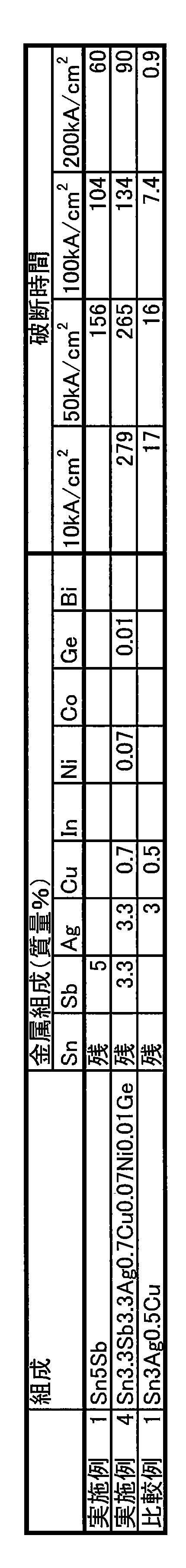
各はんだ合金の溶融性能を測定した。
各はんだ合金の固相線温度及び液相線温度を示差走査熱量測定 (Differential scanning calorimetry;DSC法)で昇温速度10K/minにて測定した。
結果を表1に示す。
また、実施例は固相線温度が230℃以上であり且つ液相線温度が240℃であった。すなわち、実施例では溶融性能が適切な範囲に調整されていた。
以上より、各実施例では、幅広い電流密度の範囲において確実にエレクトロマイグレーションの発生が抑制されていたことが明らかである。
Claims (7)
- Sbを3.0質量%超10質量%以下含み、残部としてSnを含む鉛フリーはんだ合金。
- 残部としてさらに、Ag、Cu、Ni、Co及びGeからなる群から選択される少なくとも一種の金属を含む請求項1に記載の鉛フリーはんだ合金。
- 前記Agを4.0質量%以下含む請求項2に記載の鉛フリーはんだ合金。
- 前記Cuを1.0質量%以下含む請求項2又は3に記載の鉛フリーはんだ合金。
- 前記Ni、Co及びGeを合計で0.1質量%以下含む請求項2乃至4のいずれか一項に記載の鉛フリーはんだ合金。
- 請求項1乃至5のいずれか一項に記載の鉛フリーはんだ合金と、フラックスとを含むはんだ材料。
- 電極を有する基板と半導体素子とがはんだ接合部を介して接合された接合構造体であって、前記はんだ接合部は、請求項1乃至5のいずれか一項に記載の鉛フリーはんだ合金を含む接合構造体。
Priority Applications (4)
| Application Number | Priority Date | Filing Date | Title |
|---|---|---|---|
| JP2016504153A JP6713106B2 (ja) | 2014-02-24 | 2015-02-19 | 鉛フリーはんだ合金、はんだ材料及び接合構造体 |
| US15/120,937 US9764430B2 (en) | 2014-02-24 | 2015-02-19 | Lead-free solder alloy, solder material and joined structure |
| CN201580009860.4A CN106061669A (zh) | 2014-02-24 | 2015-02-19 | 无铅钎焊合金、钎焊材料及接合结构体 |
| EP15752620.3A EP3112080A4 (en) | 2014-02-24 | 2015-02-19 | Lead-free solder alloy, solder material, and joined structure |
Applications Claiming Priority (2)
| Application Number | Priority Date | Filing Date | Title |
|---|---|---|---|
| JP2014-033234 | 2014-02-24 | ||
| JP2014033234 | 2014-02-24 |
Publications (1)
| Publication Number | Publication Date |
|---|---|
| WO2015125855A1 true WO2015125855A1 (ja) | 2015-08-27 |
Family
ID=53878354
Family Applications (1)
| Application Number | Title | Priority Date | Filing Date |
|---|---|---|---|
| PCT/JP2015/054581 WO2015125855A1 (ja) | 2014-02-24 | 2015-02-19 | 鉛フリーはんだ合金、はんだ材料及び接合構造体 |
Country Status (5)
| Country | Link |
|---|---|
| US (1) | US9764430B2 (ja) |
| EP (1) | EP3112080A4 (ja) |
| JP (1) | JP6713106B2 (ja) |
| CN (1) | CN106061669A (ja) |
| WO (1) | WO2015125855A1 (ja) |
Cited By (4)
| Publication number | Priority date | Publication date | Assignee | Title |
|---|---|---|---|---|
| JP2017170465A (ja) * | 2016-03-22 | 2017-09-28 | 株式会社タムラ製作所 | 鉛フリーはんだ合金、電子回路基板および電子制御装置 |
| WO2017217145A1 (ja) * | 2016-06-16 | 2017-12-21 | 富士電機株式会社 | はんだ接合部 |
| WO2018168858A1 (ja) * | 2017-03-17 | 2018-09-20 | 富士電機株式会社 | はんだ材 |
| US10456872B2 (en) | 2017-09-08 | 2019-10-29 | Tamura Corporation | Lead-free solder alloy, electronic circuit substrate, and electronic device |
Families Citing this family (5)
| Publication number | Priority date | Publication date | Assignee | Title |
|---|---|---|---|---|
| BR112018068596A2 (pt) | 2016-03-22 | 2019-02-12 | Tamura Corporation | liga de soldas sem chumbo, composição de fluxo, composição de pasta de solda, placa de circuito eletrônico, e controlador eletrônico |
| ES2921678T3 (es) * | 2017-09-14 | 2022-08-30 | Tamura Seisakusho Kk | Aleación de soldadura sin plomo, sustrato de circuito electrónico y dispositivo de control electrónico |
| JP6292342B1 (ja) * | 2017-09-20 | 2018-03-14 | 千住金属工業株式会社 | Cu管及び/又はFe管接合用はんだ合金、プリフォームはんだ、やに入りはんだおよびはんだ継手 |
| US11815957B2 (en) | 2019-12-10 | 2023-11-14 | Asahi Kasei Kabushiki Kaisha | Conductive film and roll thereof |
| CN111843279A (zh) * | 2020-07-22 | 2020-10-30 | 昆山市宏嘉焊锡制造有限公司 | 一种高温抗氧化的SnSbCu无铅焊料 |
Citations (8)
| Publication number | Priority date | Publication date | Assignee | Title |
|---|---|---|---|---|
| JPS527422B2 (ja) * | 1972-08-19 | 1977-03-02 | ||
| JPS5545316B2 (ja) * | 1977-10-24 | 1980-11-17 | ||
| JPH1177368A (ja) * | 1997-09-02 | 1999-03-23 | Senju Metal Ind Co Ltd | 鉛フリーはんだ合金 |
| JP2001244622A (ja) * | 2000-03-01 | 2001-09-07 | Hitachi Ltd | 電子回路装置 |
| JP2003001483A (ja) * | 2002-03-27 | 2003-01-08 | Murata Mfg Co Ltd | 半田および半田付け物品 |
| JP2004526309A (ja) * | 2001-02-08 | 2004-08-26 | インターナショナル・ビジネス・マシーンズ・コーポレーション | 電子構造体の形成方法 |
| JP2008221330A (ja) * | 2007-03-16 | 2008-09-25 | Fuji Electric Holdings Co Ltd | はんだ合金 |
| JP2011005521A (ja) * | 2009-06-25 | 2011-01-13 | Mitsui Mining & Smelting Co Ltd | Sn−Sb系半田合金 |
Family Cites Families (32)
| Publication number | Priority date | Publication date | Assignee | Title |
|---|---|---|---|---|
| JPS526468A (en) * | 1975-07-04 | 1977-01-18 | Sumitomo Metal Mining Co Ltd | Brazing material |
| JPS6186091A (ja) * | 1984-10-03 | 1986-05-01 | Furukawa Electric Co Ltd:The | Sn−Sb系合金はんだ |
| JPS6188996A (ja) * | 1984-10-05 | 1986-05-07 | Furukawa Electric Co Ltd:The | Sn−Sb系合金はんだ |
| JP2669825B2 (ja) | 1987-07-03 | 1997-10-29 | 東芝エンジニアリング株式会社 | バルブ施錠装置 |
| JPH0416897A (ja) | 1990-05-10 | 1992-01-21 | Mitsubishi Electric Corp | マルチウインド表示方式 |
| JP3027441B2 (ja) * | 1991-07-08 | 2000-04-04 | 千住金属工業株式会社 | 高温はんだ |
| US5405577A (en) * | 1993-04-29 | 1995-04-11 | Seelig; Karl F. | Lead-free and bismuth-free tin alloy solder composition |
| JPH07284983A (ja) * | 1994-04-20 | 1995-10-31 | Tanaka Denshi Kogyo Kk | 半田材料及びその製造方法 |
| JPH08174276A (ja) * | 1994-12-21 | 1996-07-09 | Tanaka Denshi Kogyo Kk | 複合半田材料及びその製造方法 |
| US6179935B1 (en) * | 1997-04-16 | 2001-01-30 | Fuji Electric Co., Ltd. | Solder alloys |
| JP3353662B2 (ja) * | 1997-08-07 | 2002-12-03 | 富士電機株式会社 | はんだ合金 |
| JP3353640B2 (ja) * | 1997-04-16 | 2002-12-03 | 富士電機株式会社 | はんだ合金 |
| JPH11291083A (ja) * | 1998-04-14 | 1999-10-26 | Murata Mfg Co Ltd | 半田合金 |
| US20030021718A1 (en) * | 2001-06-28 | 2003-01-30 | Osamu Munekata | Lead-free solder alloy |
| JP4016897B2 (ja) | 2003-06-27 | 2007-12-05 | トヨタ自動車株式会社 | 蓄電装置の充放電制御装置および自動車 |
| TW200603932A (en) * | 2004-03-19 | 2006-02-01 | Senju Metal Industry Co | Lead free solder fall |
| JP4635715B2 (ja) * | 2005-05-20 | 2011-02-23 | 富士電機システムズ株式会社 | はんだ合金およびそれを用いた半導体装置 |
| CN102196881B (zh) * | 2008-10-24 | 2014-06-04 | 三菱电机株式会社 | 半导体装置 |
| JP4554713B2 (ja) * | 2009-01-27 | 2010-09-29 | 株式会社日本フィラーメタルズ | 無鉛はんだ合金及び該はんだ合金を含む耐疲労性はんだ接合材並びに該接合材を使用した接合体 |
| JP5584427B2 (ja) * | 2009-04-14 | 2014-09-03 | 新日鉄住金マテリアルズ株式会社 | 無鉛ハンダ合金、ハンダボール及びハンダバンプを有する電子部材 |
| JP5463845B2 (ja) * | 2009-10-15 | 2014-04-09 | 三菱電機株式会社 | 電力半導体装置とその製造方法 |
| JP5486282B2 (ja) * | 2009-12-08 | 2014-05-07 | 荒川化学工業株式会社 | はんだペースト用フラックス及びはんだペースト |
| JP5486281B2 (ja) * | 2009-12-08 | 2014-05-07 | 荒川化学工業株式会社 | はんだペースト |
| JP2011138968A (ja) * | 2009-12-28 | 2011-07-14 | Senju Metal Ind Co Ltd | 面実装部品のはんだ付け方法および面実装部品 |
| JP5553181B2 (ja) * | 2010-06-01 | 2014-07-16 | 千住金属工業株式会社 | 無洗浄鉛フリーソルダペースト |
| JP5756933B2 (ja) * | 2010-09-29 | 2015-07-29 | 株式会社弘輝 | フラックス |
| WO2012077228A1 (ja) * | 2010-12-10 | 2012-06-14 | 三菱電機株式会社 | 無鉛はんだ合金、半導体装置、および半導体装置の製造方法 |
| JP6165411B2 (ja) | 2011-12-26 | 2017-07-19 | 富士通株式会社 | 電子部品及び電子機器 |
| JP5545316B2 (ja) | 2012-04-11 | 2014-07-09 | 大日本印刷株式会社 | 印画物作製装置及び印画物作製方法 |
| JP2013252548A (ja) | 2012-06-08 | 2013-12-19 | Nihon Almit Co Ltd | 微細部品接合用のソルダペースト |
| JP5893528B2 (ja) | 2012-07-27 | 2016-03-23 | 新日鉄住金マテリアルズ株式会社 | 無鉛はんだバンプ接合構造 |
| JP2014157858A (ja) * | 2013-02-14 | 2014-08-28 | Fuji Electric Co Ltd | 半導体装置の製造方法 |
-
2015
- 2015-02-19 US US15/120,937 patent/US9764430B2/en active Active
- 2015-02-19 JP JP2016504153A patent/JP6713106B2/ja active Active
- 2015-02-19 EP EP15752620.3A patent/EP3112080A4/en not_active Withdrawn
- 2015-02-19 CN CN201580009860.4A patent/CN106061669A/zh active Pending
- 2015-02-19 WO PCT/JP2015/054581 patent/WO2015125855A1/ja active Application Filing
Patent Citations (8)
| Publication number | Priority date | Publication date | Assignee | Title |
|---|---|---|---|---|
| JPS527422B2 (ja) * | 1972-08-19 | 1977-03-02 | ||
| JPS5545316B2 (ja) * | 1977-10-24 | 1980-11-17 | ||
| JPH1177368A (ja) * | 1997-09-02 | 1999-03-23 | Senju Metal Ind Co Ltd | 鉛フリーはんだ合金 |
| JP2001244622A (ja) * | 2000-03-01 | 2001-09-07 | Hitachi Ltd | 電子回路装置 |
| JP2004526309A (ja) * | 2001-02-08 | 2004-08-26 | インターナショナル・ビジネス・マシーンズ・コーポレーション | 電子構造体の形成方法 |
| JP2003001483A (ja) * | 2002-03-27 | 2003-01-08 | Murata Mfg Co Ltd | 半田および半田付け物品 |
| JP2008221330A (ja) * | 2007-03-16 | 2008-09-25 | Fuji Electric Holdings Co Ltd | はんだ合金 |
| JP2011005521A (ja) * | 2009-06-25 | 2011-01-13 | Mitsui Mining & Smelting Co Ltd | Sn−Sb系半田合金 |
Non-Patent Citations (1)
| Title |
|---|
| See also references of EP3112080A4 * |
Cited By (10)
| Publication number | Priority date | Publication date | Assignee | Title |
|---|---|---|---|---|
| JP2017170465A (ja) * | 2016-03-22 | 2017-09-28 | 株式会社タムラ製作所 | 鉛フリーはんだ合金、電子回路基板および電子制御装置 |
| WO2017217145A1 (ja) * | 2016-06-16 | 2017-12-21 | 富士電機株式会社 | はんだ接合部 |
| CN108290250A (zh) * | 2016-06-16 | 2018-07-17 | 富士电机株式会社 | 软钎焊接合部 |
| JPWO2017217145A1 (ja) * | 2016-06-16 | 2018-11-01 | 富士電機株式会社 | はんだ接合部 |
| US10504868B2 (en) | 2016-06-16 | 2019-12-10 | Fuji Electric Co., Ltd. | Solder joining |
| CN108290250B (zh) * | 2016-06-16 | 2020-07-07 | 富士电机株式会社 | 软钎焊接合部 |
| WO2018168858A1 (ja) * | 2017-03-17 | 2018-09-20 | 富士電機株式会社 | はんだ材 |
| JPWO2018168858A1 (ja) * | 2017-03-17 | 2019-11-07 | 富士電機株式会社 | はんだ材 |
| US11850685B2 (en) | 2017-03-17 | 2023-12-26 | Fuji Electric Co., Ltd. | Solder material |
| US10456872B2 (en) | 2017-09-08 | 2019-10-29 | Tamura Corporation | Lead-free solder alloy, electronic circuit substrate, and electronic device |
Also Published As
| Publication number | Publication date |
|---|---|
| US20160368104A1 (en) | 2016-12-22 |
| EP3112080A4 (en) | 2017-11-29 |
| CN106061669A (zh) | 2016-10-26 |
| JP6713106B2 (ja) | 2020-06-24 |
| US9764430B2 (en) | 2017-09-19 |
| EP3112080A1 (en) | 2017-01-04 |
| JPWO2015125855A1 (ja) | 2017-03-30 |
Similar Documents
| Publication | Publication Date | Title |
|---|---|---|
| JP6713106B2 (ja) | 鉛フリーはんだ合金、はんだ材料及び接合構造体 | |
| JP6842500B2 (ja) | 無鉛ソルダーペースト及びその製造方法 | |
| JP4753090B2 (ja) | はんだペースト、及び電子装置 | |
| KR102566561B1 (ko) | 땜납 합금, 솔더 페이스트 및 전자 회로 기판 | |
| JP5664664B2 (ja) | 接合方法、電子装置の製造方法、および電子部品 | |
| TWI505898B (zh) | A bonding method, a bonding structure, and a method for manufacturing the same | |
| JP6828880B2 (ja) | はんだペースト、はんだ合金粉 | |
| JP6387522B2 (ja) | 実装構造体 | |
| JP4722751B2 (ja) | 粉末はんだ材料および接合材料 | |
| JP6060199B2 (ja) | はんだ合金、ソルダペーストおよび電子回路基板 | |
| JP6349615B1 (ja) | はんだ合金、はんだ接合材料及び電子回路基板 | |
| JP2006294600A (ja) | 導電性接着剤 | |
| JP3782743B2 (ja) | ハンダ用組成物、ハンダ付け方法および電子部品 | |
| JP6708942B1 (ja) | はんだ合金、はんだペースト、プリフォームはんだ、はんだボール、線はんだ、脂入りはんだ、はんだ継手、電子回路基板および多層電子回路基板 | |
| WO2016114028A1 (ja) | 導電性材料、それを用いた接続方法、および接続構造 | |
| JP2016059943A (ja) | ボール状Au−Ge−Sn系はんだ合金及び該はんだ合金を用いた電子部品 | |
| JP5979083B2 (ja) | PbフリーAu−Ge−Sn系はんだ合金 | |
| JP2005297011A (ja) | ソルダーペーストおよび半田付け物品 | |
| JP7068370B2 (ja) | はんだ合金、はんだボールおよびはんだ継手 | |
| WO2016157971A1 (ja) | はんだペースト | |
| KR20170097283A (ko) | 무연 솔더 합금 조성물 및 그의 제조 방법 | |
| JP2015136735A (ja) | ボール状Au−Sn−Ag系はんだ合金並びにこのボール状Au−Sn−Ag系はんだ合金を用いて封止された電子部品及び電子部品搭載装置 |
Legal Events
| Date | Code | Title | Description |
|---|---|---|---|
| 121 | Ep: the epo has been informed by wipo that ep was designated in this application |
Ref document number: 15752620 Country of ref document: EP Kind code of ref document: A1 |
|
| ENP | Entry into the national phase |
Ref document number: 2016504153 Country of ref document: JP Kind code of ref document: A |
|
| WWE | Wipo information: entry into national phase |
Ref document number: 15120937 Country of ref document: US |
|
| NENP | Non-entry into the national phase |
Ref country code: DE |
|
| REEP | Request for entry into the european phase |
Ref document number: 2015752620 Country of ref document: EP |
|
| WWE | Wipo information: entry into national phase |
Ref document number: 2015752620 Country of ref document: EP |