WO2015098167A1 - 絶縁ゲート型半導体装置の製造方法及び絶縁ゲート型半導体装置 - Google Patents
絶縁ゲート型半導体装置の製造方法及び絶縁ゲート型半導体装置 Download PDFInfo
- Publication number
- WO2015098167A1 WO2015098167A1 PCT/JP2014/070520 JP2014070520W WO2015098167A1 WO 2015098167 A1 WO2015098167 A1 WO 2015098167A1 JP 2014070520 W JP2014070520 W JP 2014070520W WO 2015098167 A1 WO2015098167 A1 WO 2015098167A1
- Authority
- WO
- WIPO (PCT)
- Prior art keywords
- region
- conductivity type
- type impurity
- outer peripheral
- trench
- Prior art date
Links
Images

Classifications
-
- H—ELECTRICITY
- H10—SEMICONDUCTOR DEVICES; ELECTRIC SOLID-STATE DEVICES NOT OTHERWISE PROVIDED FOR
- H10D—INORGANIC ELECTRIC SEMICONDUCTOR DEVICES
- H10D30/00—Field-effect transistors [FET]
- H10D30/60—Insulated-gate field-effect transistors [IGFET]
- H10D30/64—Double-diffused metal-oxide semiconductor [DMOS] FETs
- H10D30/66—Vertical DMOS [VDMOS] FETs
- H10D30/665—Vertical DMOS [VDMOS] FETs having edge termination structures
-
- H—ELECTRICITY
- H01—ELECTRIC ELEMENTS
- H01L—SEMICONDUCTOR DEVICES NOT COVERED BY CLASS H10
- H01L21/00—Processes or apparatus adapted for the manufacture or treatment of semiconductor or solid state devices or of parts thereof
- H01L21/70—Manufacture or treatment of devices consisting of a plurality of solid state components formed in or on a common substrate or of parts thereof; Manufacture of integrated circuit devices or of parts thereof
- H01L21/71—Manufacture of specific parts of devices defined in group H01L21/70
- H01L21/76—Making of isolation regions between components
- H01L21/761—PN junctions
-
- H—ELECTRICITY
- H01—ELECTRIC ELEMENTS
- H01L—SEMICONDUCTOR DEVICES NOT COVERED BY CLASS H10
- H01L21/00—Processes or apparatus adapted for the manufacture or treatment of semiconductor or solid state devices or of parts thereof
- H01L21/70—Manufacture or treatment of devices consisting of a plurality of solid state components formed in or on a common substrate or of parts thereof; Manufacture of integrated circuit devices or of parts thereof
- H01L21/71—Manufacture of specific parts of devices defined in group H01L21/70
- H01L21/76—Making of isolation regions between components
- H01L21/762—Dielectric regions, e.g. EPIC dielectric isolation, LOCOS; Trench refilling techniques, SOI technology, use of channel stoppers
- H01L21/76224—Dielectric regions, e.g. EPIC dielectric isolation, LOCOS; Trench refilling techniques, SOI technology, use of channel stoppers using trench refilling with dielectric materials
- H01L21/76237—Dielectric regions, e.g. EPIC dielectric isolation, LOCOS; Trench refilling techniques, SOI technology, use of channel stoppers using trench refilling with dielectric materials introducing impurities in trench side or bottom walls, e.g. for forming channel stoppers or alter isolation behavior
-
- H—ELECTRICITY
- H10—SEMICONDUCTOR DEVICES; ELECTRIC SOLID-STATE DEVICES NOT OTHERWISE PROVIDED FOR
- H10D—INORGANIC ELECTRIC SEMICONDUCTOR DEVICES
- H10D12/00—Bipolar devices controlled by the field effect, e.g. insulated-gate bipolar transistors [IGBT]
- H10D12/01—Manufacture or treatment
- H10D12/031—Manufacture or treatment of IGBTs
- H10D12/032—Manufacture or treatment of IGBTs of vertical IGBTs
- H10D12/038—Manufacture or treatment of IGBTs of vertical IGBTs having a recessed gate, e.g. trench-gate IGBTs
-
- H—ELECTRICITY
- H10—SEMICONDUCTOR DEVICES; ELECTRIC SOLID-STATE DEVICES NOT OTHERWISE PROVIDED FOR
- H10D—INORGANIC ELECTRIC SEMICONDUCTOR DEVICES
- H10D12/00—Bipolar devices controlled by the field effect, e.g. insulated-gate bipolar transistors [IGBT]
- H10D12/411—Insulated-gate bipolar transistors [IGBT]
- H10D12/441—Vertical IGBTs
- H10D12/461—Vertical IGBTs having non-planar surfaces, e.g. having trenches, recesses or pillars in the surfaces of the emitter, base or collector regions
- H10D12/481—Vertical IGBTs having non-planar surfaces, e.g. having trenches, recesses or pillars in the surfaces of the emitter, base or collector regions having gate structures on slanted surfaces, on vertical surfaces, or in grooves, e.g. trench gate IGBTs
-
- H—ELECTRICITY
- H10—SEMICONDUCTOR DEVICES; ELECTRIC SOLID-STATE DEVICES NOT OTHERWISE PROVIDED FOR
- H10D—INORGANIC ELECTRIC SEMICONDUCTOR DEVICES
- H10D30/00—Field-effect transistors [FET]
- H10D30/01—Manufacture or treatment
- H10D30/021—Manufacture or treatment of FETs having insulated gates [IGFET]
- H10D30/028—Manufacture or treatment of FETs having insulated gates [IGFET] of double-diffused metal oxide semiconductor [DMOS] FETs
- H10D30/0291—Manufacture or treatment of FETs having insulated gates [IGFET] of double-diffused metal oxide semiconductor [DMOS] FETs of vertical DMOS [VDMOS] FETs
- H10D30/0297—Manufacture or treatment of FETs having insulated gates [IGFET] of double-diffused metal oxide semiconductor [DMOS] FETs of vertical DMOS [VDMOS] FETs using recessing of the gate electrodes, e.g. to form trench gate electrodes
-
- H—ELECTRICITY
- H10—SEMICONDUCTOR DEVICES; ELECTRIC SOLID-STATE DEVICES NOT OTHERWISE PROVIDED FOR
- H10D—INORGANIC ELECTRIC SEMICONDUCTOR DEVICES
- H10D30/00—Field-effect transistors [FET]
- H10D30/60—Insulated-gate field-effect transistors [IGFET]
- H10D30/64—Double-diffused metal-oxide semiconductor [DMOS] FETs
- H10D30/66—Vertical DMOS [VDMOS] FETs
- H10D30/668—Vertical DMOS [VDMOS] FETs having trench gate electrodes, e.g. UMOS transistors
-
- H—ELECTRICITY
- H10—SEMICONDUCTOR DEVICES; ELECTRIC SOLID-STATE DEVICES NOT OTHERWISE PROVIDED FOR
- H10D—INORGANIC ELECTRIC SEMICONDUCTOR DEVICES
- H10D62/00—Semiconductor bodies, or regions thereof, of devices having potential barriers
- H10D62/10—Shapes, relative sizes or dispositions of the regions of the semiconductor bodies; Shapes of the semiconductor bodies
- H10D62/102—Constructional design considerations for preventing surface leakage or controlling electric field concentration
- H10D62/103—Constructional design considerations for preventing surface leakage or controlling electric field concentration for increasing or controlling the breakdown voltage of reverse-biased devices
- H10D62/104—Constructional design considerations for preventing surface leakage or controlling electric field concentration for increasing or controlling the breakdown voltage of reverse-biased devices having particular shapes of the bodies at or near reverse-biased junctions, e.g. having bevels or moats
-
- H—ELECTRICITY
- H10—SEMICONDUCTOR DEVICES; ELECTRIC SOLID-STATE DEVICES NOT OTHERWISE PROVIDED FOR
- H10D—INORGANIC ELECTRIC SEMICONDUCTOR DEVICES
- H10D62/00—Semiconductor bodies, or regions thereof, of devices having potential barriers
- H10D62/10—Shapes, relative sizes or dispositions of the regions of the semiconductor bodies; Shapes of the semiconductor bodies
- H10D62/102—Constructional design considerations for preventing surface leakage or controlling electric field concentration
- H10D62/103—Constructional design considerations for preventing surface leakage or controlling electric field concentration for increasing or controlling the breakdown voltage of reverse-biased devices
- H10D62/105—Constructional design considerations for preventing surface leakage or controlling electric field concentration for increasing or controlling the breakdown voltage of reverse-biased devices by having particular doping profiles, shapes or arrangements of PN junctions; by having supplementary regions, e.g. junction termination extension [JTE]
- H10D62/106—Constructional design considerations for preventing surface leakage or controlling electric field concentration for increasing or controlling the breakdown voltage of reverse-biased devices by having particular doping profiles, shapes or arrangements of PN junctions; by having supplementary regions, e.g. junction termination extension [JTE] having supplementary regions doped oppositely to or in rectifying contact with regions of the semiconductor bodies, e.g. guard rings with PN or Schottky junctions
- H10D62/107—Buried supplementary regions, e.g. buried guard rings
-
- H—ELECTRICITY
- H10—SEMICONDUCTOR DEVICES; ELECTRIC SOLID-STATE DEVICES NOT OTHERWISE PROVIDED FOR
- H10D—INORGANIC ELECTRIC SEMICONDUCTOR DEVICES
- H10D62/00—Semiconductor bodies, or regions thereof, of devices having potential barriers
- H10D62/10—Shapes, relative sizes or dispositions of the regions of the semiconductor bodies; Shapes of the semiconductor bodies
- H10D62/113—Isolations within a component, i.e. internal isolations
- H10D62/115—Dielectric isolations, e.g. air gaps
-
- H—ELECTRICITY
- H10—SEMICONDUCTOR DEVICES; ELECTRIC SOLID-STATE DEVICES NOT OTHERWISE PROVIDED FOR
- H10D—INORGANIC ELECTRIC SEMICONDUCTOR DEVICES
- H10D64/00—Electrodes of devices having potential barriers
- H10D64/20—Electrodes characterised by their shapes, relative sizes or dispositions
- H10D64/27—Electrodes not carrying the current to be rectified, amplified, oscillated or switched, e.g. gates
- H10D64/311—Gate electrodes for field-effect devices
- H10D64/411—Gate electrodes for field-effect devices for FETs
- H10D64/511—Gate electrodes for field-effect devices for FETs for IGFETs
- H10D64/514—Gate electrodes for field-effect devices for FETs for IGFETs characterised by the insulating layers
- H10D64/516—Gate electrodes for field-effect devices for FETs for IGFETs characterised by the insulating layers the thicknesses being non-uniform
-
- H—ELECTRICITY
- H01—ELECTRIC ELEMENTS
- H01L—SEMICONDUCTOR DEVICES NOT COVERED BY CLASS H10
- H01L21/00—Processes or apparatus adapted for the manufacture or treatment of semiconductor or solid state devices or of parts thereof
- H01L21/02—Manufacture or treatment of semiconductor devices or of parts thereof
- H01L21/04—Manufacture or treatment of semiconductor devices or of parts thereof the devices having potential barriers, e.g. a PN junction, depletion layer or carrier concentration layer
- H01L21/0445—Manufacture or treatment of semiconductor devices or of parts thereof the devices having potential barriers, e.g. a PN junction, depletion layer or carrier concentration layer the devices having semiconductor bodies comprising crystalline silicon carbide
- H01L21/0455—Making n or p doped regions or layers, e.g. using diffusion
- H01L21/046—Making n or p doped regions or layers, e.g. using diffusion using ion implantation
-
- H—ELECTRICITY
- H10—SEMICONDUCTOR DEVICES; ELECTRIC SOLID-STATE DEVICES NOT OTHERWISE PROVIDED FOR
- H10D—INORGANIC ELECTRIC SEMICONDUCTOR DEVICES
- H10D12/00—Bipolar devices controlled by the field effect, e.g. insulated-gate bipolar transistors [IGBT]
- H10D12/01—Manufacture or treatment
- H10D12/031—Manufacture or treatment of IGBTs
-
- H—ELECTRICITY
- H10—SEMICONDUCTOR DEVICES; ELECTRIC SOLID-STATE DEVICES NOT OTHERWISE PROVIDED FOR
- H10D—INORGANIC ELECTRIC SEMICONDUCTOR DEVICES
- H10D62/00—Semiconductor bodies, or regions thereof, of devices having potential barriers
- H10D62/80—Semiconductor bodies, or regions thereof, of devices having potential barriers characterised by the materials
- H10D62/83—Semiconductor bodies, or regions thereof, of devices having potential barriers characterised by the materials being Group IV materials, e.g. B-doped Si or undoped Ge
- H10D62/832—Semiconductor bodies, or regions thereof, of devices having potential barriers characterised by the materials being Group IV materials, e.g. B-doped Si or undoped Ge being Group IV materials comprising two or more elements, e.g. SiGe
- H10D62/8325—Silicon carbide
Definitions
- the technology disclosed in this specification relates to an insulated gate semiconductor device.
- Patent Document 1 discloses an insulated gate semiconductor device having an element region in which a MOS structure is formed and an outer peripheral region around the region. A plurality of gate trenches are formed in the element region, and a gate insulating film and a gate electrode are formed in the gate trench. A p-type bottom surface surrounding region (hereinafter referred to as an element portion bottom surface surrounding region) is formed in a range exposed at the bottom surface of the gate trench. A plurality of trenches are formed in the outer peripheral region so as to surround the element region, and an insulating layer is filled in each trench.
- a p-type bottom surface surrounding region (hereinafter referred to as an outer peripheral portion bottom surface surrounding region) is formed in a range exposed on the bottom surface of each trench in the outer peripheral region.
- an outer peripheral portion bottom surface surrounding region is formed in a range exposed on the bottom surface of each trench in the outer peripheral region.
- the depletion layer When the depletion layer reaches the second outer peripheral bottom surface surrounding region, the depletion layer extends from the second outer peripheral bottom surface surrounding region toward the third outer peripheral bottom surface surrounding region. In this way, the depletion layer sequentially spreads through the outer peripheral bottom surface surrounding area. For this reason, depletion progresses only from one side in the drift region sandwiched between the two outer peripheral bottom surface surrounding regions. For this reason, the outer peripheral region is not easily depleted. Therefore, it is desired to further increase the breakdown voltage in the outer peripheral region.
- a semiconductor substrate, a front surface electrode formed on the surface of the semiconductor substrate, and a back surface electrode formed on the back surface of the semiconductor substrate, the front surface electrode and the back surface are provided.
- An insulated gate semiconductor device that switches between electrodes is manufactured.
- the insulated gate semiconductor device includes a first conductivity type first region connected to the surface electrode, a second conductivity type second region in contact with the first region, and the second region.
- a gate insulating film and a gate electrode disposed in the gate trench a fourth region of the second conductivity type formed in a range exposed at the bottom surface of the gate trench, and a region outside the second region
- the manufacturing method includes the step of forming the gate trench, the step of forming the outer peripheral trench, implanting a first p-type impurity into the bottom surface of the gate trench, and diffusing the implanted first p-type impurity. Forming a fourth region; and implanting a second p-type impurity into the bottom surface of the outer peripheral trench and diffusing the implanted second p-type impurity to form the fifth region.
- the diffusion coefficient of the second p-type impurity in the step of forming the fifth region is larger than the diffusion coefficient of the first p-type impurity in the step of forming the fourth region.
- either the gate trench or the outer periphery trench may be formed first. Further, either the impurity implantation into the bottom surface of the gate trench or the impurity implantation into the bottom surface of the outer peripheral trench may be performed first. Further, the diffusion of the impurity implanted into the bottom surface of the gate trench and the diffusion of the impurity implanted into the bottom surface of the outer peripheral trench may be performed first, or these may be performed simultaneously.
- the diffusion coefficient of the second p-type impurity in the step of forming the fifth region is large. Therefore, the fifth region having a wider width can be formed by diffusing the second p-type impurity in a wider range. For this reason, it is possible to narrow the space
- the diffusion coefficient of the first p-type impurity in the step of forming the fourth region is small. Accordingly, the diffusion range of the first p-type impurity is narrowed, and thereby the width of the fourth region is narrowed. Thus, by narrowing the width of the fourth region, it is possible to ensure a wide interval (that is, a current path) between the fourth regions. As a result, the on-voltage of the insulated gate semiconductor device can be reduced.
- the first p-type impurity may be an element different from the second p-type impurity.
- the first p-type impurity and the second p-type impurity are boron, and boron and carbon may be implanted into the bottom surface of the gate trench in the step of forming the fourth region. .
- the diffusion coefficient of the second p-type impurity in the step of forming the fifth region can be made larger than the diffusion coefficient of the first p-type impurity in the step of forming the fourth region.
- the step of forming the fifth region in the step of forming the fifth region, the step of forming the second region on the bottom surface of the outer peripheral trench and the fourth region based on the second p-type impurity.
- a third p-type impurity having a small diffusion coefficient may be implanted.
- the second p-type impurity is implanted at a concentration at which at least a part of the semiconductor layer constituting the bottom surface of the outer peripheral trench becomes amorphous. Also good.
- the second p-type impurity in the step of forming the fifth region, may be implanted into the bottom surface of the outer peripheral trench at a concentration of 1 ⁇ 10 18 atoms / cm 3 or more. .
- Any of these methods can increase the p-type impurity concentration in the region around the bottom surface of the outer peripheral trench in the fifth region. Thereby, it is possible to suppress the generation of a high electric field in the vicinity of the bottom surface of the outer peripheral trench.
- the interval between the fifth regions may be 1 ⁇ 2 or less of the interval between the fourth regions.
- the avalanche breakdown occurs in the element portion earlier than the outer peripheral portion. Since the element portion has high avalanche resistance, the breakdown voltage of the insulated gate semiconductor device is improved by causing the avalanche breakdown first in the element portion.
- the present specification also proposes a new insulated gate semiconductor device.
- the insulated gate semiconductor device includes a semiconductor substrate, a surface electrode formed on a surface of the semiconductor substrate, and a back electrode formed on a back surface of the semiconductor substrate. Switching between.
- the insulated gate semiconductor device includes a first conductivity type first region connected to the surface electrode, a second conductivity type second region in contact with the first region, and the second region.
- a third region of the first conductivity type separated from the first region, and a plurality of regions reaching the third region through the first region and the second region, formed on the surface of the semiconductor substrate A gate trench, a gate insulating film and a gate electrode disposed in the gate trench, a second conductivity type fourth region formed in a range exposed at a bottom surface of the gate trench, and the second region
- the width of the fifth region is wider than the width of the fourth region.
- the second conductivity type impurity contained in the fourth region may be an element different from the second conductivity type impurity contained in the fifth region.
- the second conductivity type impurity contained in the fourth region and the second conductivity type impurity contained in the fifth region may be boron, and the fourth region may further contain carbon.
- a first specific second conductivity type impurity and a second specific second conductivity type impurity having a smaller diffusion coefficient in the semiconductor substrate than the first specific second conductivity type impurity. May be included.
- At least a part of the bottom surface of the outer peripheral trench may be an amorphous layer.
- At least a part of the bottom surface of the outer peripheral trench may contain the second conductivity type impurity at a concentration of 1 ⁇ 10 18 atoms / cm 3 or more.
- the interval between the fifth regions may be 1 ⁇ 2 or less of the interval between the fourth regions. According to such a configuration, the breakdown voltage of the insulated gate semiconductor device can be improved.
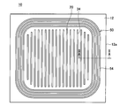
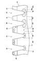
- FIG. 3 is a top view of the semiconductor device 10.
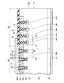
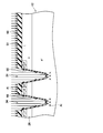
- FIG. 2 is a longitudinal sectional view of the semiconductor device 10 taken along the line II-II in FIG. 1. Explanatory drawing of the manufacturing process of the semiconductor device 10 (enlarged sectional drawing of the area
- Explanatory drawing of the manufacturing process of the semiconductor device 10 (enlarged sectional drawing of the area
- region 56 are formed). Explanatory drawing of the manufacturing process of the semiconductor device 10 (enlarged sectional drawing of the area
- region 56 are formed). Explanatory drawing of the manufacturing process of the semiconductor device 10 (enlarged sectional drawing of the area
- region 56 are formed). Explanatory drawing of the manufacturing process of the semiconductor device 10 (enlarged sectional drawing of the area
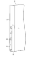
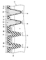
- the semiconductor device 10 shown in FIG. 1 has a semiconductor substrate 12 made of SiC.
- the semiconductor substrate 12 has a cell region 20 and an outer peripheral region 50.
- a MOSFET is formed in the cell region 20.
- the outer peripheral region 50 is a region between the cell region 20 and the end surface 12 a of the semiconductor substrate 12.
- a surface electrode 14 and an insulating layer 16 are formed on the surface of the semiconductor substrate 12.
- the insulating layer 16 covers the surface of the semiconductor substrate 12 in the outer peripheral region 50.
- the surface electrode 14 is in contact with the semiconductor substrate 12 in the cell region 20.
- the lower region of the contact region where the surface electrode 14 is in contact with the semiconductor substrate 12 is the cell region 20, and the region on the outer peripheral side (end face 12 a side) than the contact region is the outer peripheral region 50.
- a back electrode 18 is formed on the back surface of the semiconductor substrate 12. The back electrode 18 covers substantially the entire back surface of the semiconductor substrate 12.
- a source region 22 In the cell region 20, a source region 22, a body contact region 24, a body region 26, a drift region 28, a drain region 30, a p-type floating region 32, and a gate trench 34 are formed.
- the source region 22 is an n-type region containing n-type impurities at a high concentration.
- the source region 22 is formed in a range exposed on the upper surface of the semiconductor substrate 12.
- the source region 22 is ohmically connected to the surface electrode 14.
- the body contact region 24 is a p-type region containing p-type impurities at a high concentration.
- the body contact region 24 is formed so as to be exposed on the upper surface of the semiconductor substrate 12 at a position where the source region 22 is not formed.
- the body contact region 24 is ohmically connected to the surface electrode 14.
- the body region 26 is a p-type region containing p-type impurities at a low concentration.
- the p-type impurity concentration in the body region 26 is lower than the p-type impurity concentration in the body contact region 24.
- the body region 26 is formed below the source region 22 and the body contact region 24 and is in contact with these regions.
- the drift region 28 is an n-type region containing n-type impurities at a low concentration.
- the n-type impurity concentration of the drift region 28 is lower than the n-type impurity concentration of the source region 22.
- the drift region 28 is formed below the body region 26. The drift region 28 is in contact with the body region 26 and is separated from the source region 22 by the body region 26.
- the drain region 30 is an n-type region containing an n-type impurity at a high concentration.
- the n-type impurity concentration of the drain region 30 is higher than the n-type impurity concentration of the drift region 28.
- the drain region 30 is formed below the drift region 28. Drain region 30 is in contact with drift region 28 and is separated from body region 26 by drift region 28.
- the drain region 30 is formed in a range exposed on the lower surface of the semiconductor substrate 12.
- the drain region 30 is ohmically connected to the back electrode 18.
- a plurality of gate trenches 34 are formed on the upper surface of the semiconductor substrate 12 in the cell region 20. Each gate trench 34 extends linearly in parallel with each other on the surface of the semiconductor substrate 12. Each gate trench 34 is formed so as to penetrate the source region 22 and the body region 26 and reach the drift region 28.
- a bottom insulating layer 34a, a gate insulating film 34b, and a gate electrode 34c are formed in each gate trench 34.
- the bottom insulating layer 34 a is a thick insulating layer formed at the bottom of the gate trench 34.
- a side surface of the gate trench 34 above the bottom insulating layer 34a is covered with a gate insulating film 34b.
- a gate electrode 34c is formed in the gate trench 34 above the bottom insulating layer 34a.
- the gate electrode 34c is opposed to the source region 22, the body region 26, and the drift region 28 through the gate insulating film 34b.
- the gate electrode 34c is insulated from the semiconductor substrate 12 by the gate insulating film 34b and the bottom insulating layer 34a.
- the upper surface of the gate electrode 34c is covered with an insulating layer 34d.
- the gate electrode 34c is insulated from the surface electrode 14 by the insulating layer 34d.
- the p-type floating region 32 is formed in the semiconductor substrate 12 in a range in contact with the bottom surface of each gate trench 34. Each p-type floating region 32 is surrounded by a drift region 28. The p-type floating regions 32 are separated from each other by the drift region 28.
- a p-type surface region 51 is formed in a range exposed on the surface of the semiconductor substrate 12 in the outer peripheral region 50.
- the surface region 51 extends to substantially the same depth as the body region 26.
- the drift region 28 and the drain region 30 described above extend to the outer peripheral region 50.
- the drift region 28 and the drain region 30 extend to the end face 12 a of the semiconductor substrate 12.
- the drift region 28 is in contact with the surface region 51 from below.
- a plurality of outer peripheral trenches 54 are formed on the upper surface of the semiconductor substrate 12 in the outer peripheral region 50.
- Each outer peripheral trench 54 is formed so as to penetrate the surface region 51 and reach the drift region 28.
- An insulating layer 53 is formed in each outer peripheral trench 54.
- each outer periphery trench 54 is formed in an annular shape that makes a round around the cell region 20 when the semiconductor substrate 12 is viewed from above.
- Each outer peripheral trench 54 is formed at a distance from each other.
- the surface region 51 is separated from the body region 26 (that is, the p-type region connected to the surface electrode 14) by the outer peripheral trench 54. Further, the surface regions 51 are separated from each other by the outer peripheral trenches 54.
- a p-type bottom region 56 is formed in the semiconductor substrate 12 in a range in contact with the bottom surface of each outer peripheral trench 54.
- the bottom surface region 56 is formed along the outer periphery trench 54 so as to cover the entire bottom surface of the outer periphery trench 54.
- the periphery of each bottom surface region 56 is surrounded by the drift region 28.
- the bottom surface regions 56 are separated from each other by the drift region 28.
- the width W1 of each bottom surface region 56 is wider than the width W2 of each p-type floating region 32.
- the width W1 of the bottom region 56 means the dimension of the bottom region 56 in the direction crossing the outer peripheral trench 54 (that is, the width direction of the outer peripheral trench 54).
- the width W2 of the p-type floating region 32 means the dimension of the p-type floating region 32 in the direction across the gate trench 34 (that is, the width direction of the gate trench 34).
- the operation of the semiconductor device 10 will be described.
- a voltage that makes the back electrode 18 positive is applied between the back electrode 18 and the front electrode 14.
- the MOSFET in the cell region 20 is turned on by applying a gate-on voltage to the gate electrode 34c. That is, a channel is formed in the body region 26 at a position facing the gate electrode 34c, and from the front surface electrode 14 to the back surface electrode 18 via the source region 22, the channel, the drift region 28, and the drain region 30. Electrons flow. At this time, electrons flow through the drift region 28b located between the two p-type floating regions 32.
- the width W2 of each p-type floating region 32 is narrowed, and thereby the width W4 of the drift region 28b is widened.
- the width of the drift region 28b through which the current flows is secured wide, the on-voltage of the MOSFET is low.
- the channel disappears and the MOSFET is turned off.
- the MOSFET is turned off, a depletion layer spreads in the drift region 28 from the pn junction at the boundary between the body region 26 and the drift region 28.
- the depletion layer reaches the p-type floating region 32 in the cell region 20, the depletion layer also extends from the p-type floating region 32 into the drift region 28. Therefore, a depletion layer spreads from the p-type floating regions 32 on both sides in the drift region 28 b located between the two p-type floating regions 32. As described above, the depletion layer extends in the cell region 20, thereby realizing a high breakdown voltage in the cell region 20.
- the width W4 of the drift region 28b located between the two p-type floating regions 32 is wide.
- the drift region 28b is depleted from both sides. For this reason, even if the width W4 of the drift region 28b is wide, the drift region 28b is easily depleted.
- the depletion layer extending from the above-described pn junction reaches the bottom surface region 56a on the lower side of the outer peripheral trench 54 positioned closest to the cell region 20 side. Then, a depletion layer extends from the bottom surface region 56a toward the bottom surface region 56b on the outer peripheral side. When the depletion layer reaches the bottom surface region 56b, the depletion layer extends from the bottom surface region 56b toward the bottom surface region 56c on the outer peripheral side. As described above, in the outer peripheral region 50, the depletion layer extends in order to the outer peripheral side via the bottom surface regions 56, so that the depletion layer extends to the bottom surface region 56 d on the outermost peripheral side.
- the depletion layer extends in the outer peripheral region 50, thereby realizing a high breakdown voltage in the outer peripheral region 50. Since the depletion layer extends in this way in the outer peripheral region 50, the drift region 28a located between the two bottom surface regions 56 is depleted only from one side (cell region 20 side). However, the width W3 of the drift region 28a is narrow, so that the drift region 28a is surely depleted.
- the width W3 of the drift region 28a is less than 1 ⁇ 2 of the width W4 of the drift region 28b. For this reason, the drift region 28a is depleted before the drift region 28b. According to such a configuration, an avalanche breakdown can be caused in the cell region 20 when an excessive voltage is applied to the semiconductor device 10. That is, since the area of the outer peripheral region 50 is small, the current path is small, and the avalanche current density tends to increase when avalanche breakdown occurs. For this reason, the outer peripheral region 50 has a low avalanche resistance. On the other hand, since the cell region 20 has a large area and a wide current path, the avalanche current density is low even if avalanche breakdown occurs.
- the cell region 20 has a higher avalanche resistance than the outer peripheral region 50. For this reason, by making the avalanche breakdown occur in the cell region 20 as described above, the avalanche resistance of the semiconductor device 10 as a whole can be improved.
- the source region 22, the body contact region 24, the body region 26, and the surface region 51 are formed in the semiconductor substrate 12 by epitaxial growth, ion implantation, or the like.
- a mask 60 for example, an oxide film
- the semiconductor substrate 12 in the opening is etched by anisotropic etching.
- the side surface of the gate trench 34 has a tapered shape.
- a protective film 66 oxide film is formed on the inner surface of the gate trench 34 by CVD or thermal oxidation.
- the semiconductor substrate 12 is irradiated with Al (aluminum).
- Al aluminum
- the irradiated Al passes through the protective film 66 on the bottom surface of the gate trench 34 and is injected into the bottom surface of the gate trench 34. Further, the protective film 66 prevents Al from being implanted into the side surface of the gate trench 34. Therefore, Al is injected only into the bottom surface of the gate trench 34. Thereafter, the mask 60 and the protective film 66 are removed.
- a mask 61 for example, an oxide film
- the semiconductor substrate 12 in the opening is etched by anisotropic etching. Form.
- the side surface of the outer peripheral trench 54 has a tapered shape.
- a protective film 67 oxide film is formed on the inner surface of the outer peripheral trench 54 by CVD or thermal oxidation.
- B boron
- the irradiated B penetrates the protective film 67 on the bottom surface of the outer trench 54 and is injected into the bottom surface of the outer trench 54. Further, the protective film 67 prevents B from being implanted into the side surface of the outer peripheral trench 54. Therefore, B is injected only into the bottom surface of the outer peripheral trench 54. Thereafter, the mask 61 and the protective film 67 are removed.
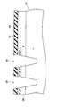
- the semiconductor substrate 12 is annealed at a temperature of 1600 ° C. or higher. Thereby, Al and B implanted into the semiconductor substrate 12 are activated. As a result, as shown in FIG. 10, the p-type floating region 32 is formed around the bottom surface of the gate trench 34, and the bottom region 56 is formed around the bottom surface of the outer peripheral trench 54.
- the diffusion coefficient of B is much larger than the diffusion coefficient of Al. For this reason, in the activation annealing step, the diffusion distance of B becomes larger than the diffusion distance of Al. For this reason, as shown in FIG.
- the size of the bottom surface region 56 (that is, the diffusion range of B) is larger than the size of the p-type floating region 32 (that is, the diffusion range of Al). Accordingly, the width W1 of the bottom region 56 is wider than the width W2 of the p-type floating region 32, and the interval W3 between the two bottom regions 56 is narrower than the interval W4 between the two p-type floating regions 32.
- necessary structures (the trench gate structure, the insulating layer 16, the front surface electrode 14, the drain region 30, and the back surface electrode 18 shown in FIG. 1) are formed, whereby the semiconductor device 10 shown in FIG. 1 is completed.
- B having a large diffusion coefficient is implanted into the bottom surface of the outer peripheral trench 54 to form the bottom region 56 having a wide width W1, while the diffusion is performed on the bottom surface of the gate trench 34.
- Al having a small coefficient is implanted to form a p-type floating region 32 having a narrow width W2.
- the width of the bottom region 56 can be made wider than the width of the p-type floating region 32.
- the width W3 between the bottom surface regions 56 can be narrowed to improve the breakdown voltage, and the current path width W4 in the cell region 20 can be widened to improve the on-voltage of the MOSFET.
- the interval W3 between the bottom surface regions 56 can also be reduced by reducing the interval between the outer peripheral trenches 54.
- the interval W3 is narrowed regardless of the limitation due to the processing accuracy of the outer peripheral trench 54. It is possible.
- the width W3 can be further reduced by narrowing the distance between the outer peripheral trenches 54 as much as possible within the limit and forming the bottom surface region 56 by B implantation.
- the first injection step described above is different from the manufacturing method of Example 1.
- Other steps are the same as those of the manufacturing method of the first embodiment.
- C carbon
- B is implanted into the bottom surface of the gate trench 34.
- C is preferably implanted at a higher concentration than B.
- B may be injected before C.
- B is implanted into the bottom surface of the outer peripheral trench 54 as in the manufacturing method of the first embodiment.
- C is not implanted into the bottom surface of the outer peripheral trench 54.
- the activation annealing step the semiconductor substrate 12 is annealed in the same manner as in the manufacturing method of Example 1, and B implanted into the semiconductor substrate 12 is diffused.
- B implanted into the bottom surface of the outer peripheral trench 54 diffuses widely as in the first embodiment.
- B implanted into the bottom surface of the gate trench 34 does not diffuse so widely. This is because the diffusion coefficient of B is low in the SiC region into which C is implanted. Therefore, as shown in FIG. 10, a bottom surface region 56 having a wide width W1 is formed around the bottom surface of the outer peripheral trench 54, and a p-type floating region 32 having a narrow width W2 is formed around the bottom surface of the gate trench 34. Is done.
- the range in which C is injected is wider than the range in which B is injected.
- B and C may be implanted into the bottom surface of the outer peripheral trench 54 also in the second implantation step of the second embodiment. Even in such a configuration, if the concentration of C injected into the bottom surface of the outer periphery trench 54 is lower than the concentration of C injected into the bottom surface of the gate trench 34, the diffusion distance of B in the vicinity of the bottom surface of the outer periphery trench 54 is It becomes longer than the diffusion distance of B in the vicinity of the bottom surface of the gate trench 34. Therefore, the bottom region 56 can be formed wider than the p-type floating region 32.
- the second injection step described above is different from the manufacturing method of Example 1.
- Other steps are the same as those of the manufacturing method of the first embodiment.
- B is implanted at a very high concentration into the bottom surface of the outer peripheral trench 54.
- B is implanted so that at least a part of the semiconductor layer constituting the bottom surface of the outer peripheral trench 54 contains B at a concentration of 1 ⁇ 10 18 atoms / cm 3 or more.
- B is implanted at such a high concentration, an extremely large number of crystal defects are generated in the region where B is implanted at a high concentration.
- the region where B is implanted at a high concentration becomes amorphous.
- the diffusion coefficient of B is low.
- FIG. 11 shows the concentration distribution of B when B is implanted into a shallow region (more specifically, a region shallower than 1000 nm) of a semiconductor substrate made of SiC.
- graph A shows the concentration distribution immediately after B is injected.
- Graphs B to E show concentration distributions after annealing for 30 minutes at the corresponding temperatures.
- the graph D and the graph E overlap.
- B is distributed only in a region shallower than 1000 nm.
- graphs B to E when heat treatment is performed, the distribution range of B is expanded in a deep direction. This indicates that B is diffused in SiC.
- the B concentration does not change so much in the graphs A to E in the region where the B concentration is 1 ⁇ 10 18 atoms / cm 3 or more. This means that B is difficult to diffuse in a region containing B at a high concentration of 1 ⁇ 10 18 atoms / cm 3 or more. It can be seen that in the region containing B at a high concentration of 1 ⁇ 10 18 atoms / cm 3 or more, since the number of defects is extremely large, the diffusion coefficient of B is small.
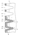
- B is implanted at a high concentration into the bottom surface of the outer peripheral trench 54 in the second implantation step, and then an activation annealing step is performed. Then, since B does not diffuse much in the region containing B at a high concentration in the vicinity of the bottom surface of the outer peripheral trench 54, a region having a high B concentration remains in the vicinity of the bottom surface of the outer peripheral trench 54. As a result, the high concentration bottom region 57 shown in FIG. 12 is formed. Further, B is diffused widely around the high concentration bottom region 57, so that a low concentration bottom region 58 is formed.
- the high-concentration bottom region 57 is a region containing B having a concentration of 1 ⁇ 10 18 atoms / cm 3 or more, and the low-concentration bottom region 58 is 1 ⁇ 10 18 atoms / cm 3. It is a region containing B at a concentration of less than.
- the high-concentration bottom region 57 may be an amorphous region. As described above, when the high-concentration bottom region 57 is formed in the vicinity of the bottom surface of the outer peripheral trench 54, the depletion layer is prevented from reaching the bottom surface of the outer peripheral trench 54 when the depletion layer extends in the outer peripheral region 50. Is done. As a result, the generation of a high electric field near the bottom surface of the outer peripheral trench 54 is suppressed. Further, since the low concentration bottom region 58 is widely distributed, the width W1 of the bottom region 56 is widened, and the breakdown voltage of the outer peripheral region 50 is improved.
- the second injection step described above is different from the manufacturing method of Example 1.
- Other steps are the same as those of the manufacturing method of the first embodiment.
- B is implanted into the bottom surface of the outer peripheral trench 54, and then Al is implanted into the bottom surface of the outer peripheral trench 54.
- Al may be injected first and B may be injected later.
- the activation annealing step the semiconductor substrate 12 is annealed in the same manner as in the manufacturing method of Example 1, and p-type impurities (that is, B and Al) implanted in the semiconductor substrate 12 are diffused.
- B and Al p-type impurities
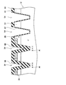
- a high concentration bottom region 57 having a high p-type impurity concentration is formed around the bottom surface of the outer peripheral trench 54, and a low concentration having a low p-type impurity concentration is formed around the high concentration bottom region 57.
- a bottom region 58 is formed.
- the high concentration bottom region 57 is a region where a large amount of Al exists
- the low concentration bottom region 58 is a region where a large amount of B exists. Therefore, even in the semiconductor device 10 manufactured by the manufacturing method of Example 4, the depletion layer is prevented from reaching the bottom surface of the outer peripheral trench 54 when the depletion layer extends in the outer peripheral region 50. As a result, the generation of a high electric field near the bottom surface of the outer peripheral trench 54 is suppressed.
- the diffusion distance of the p-type impurity in the activation annealing step is closer to the bottom surface of the outer trench 54 than the p-type impurity implanted into the bottom surface of the gate trench 34.
- the p-type impurity and the element to be implanted together with the p-type impurity are selected so as to be long with the implanted p-type impurity. Thereby, it is realized that the bottom region 56 is formed wider than the p-type floating region 32.
- Ga (gallium) or In (indium) may be used as the p-type impurity instead of Al.
- Ga and In can be used in the same manner as Al since the diffusion distance in SiC is short. Moreover, the diffusion distance of Al, Ga, and In is shorter than the diffusion distance of B when B and C are implanted. Therefore, Al, Ga, or In may be implanted into the bottom surface of the gate trench 34 in the first implantation step, and C and B may be implanted into the bottom surface of the outer peripheral trench 54 in the second implantation step. Further, the second injection process of the third and fourth embodiments may be applied to the second embodiment.
- a SiC semiconductor substrate is used, but other semiconductor substrates may be used.
- the diffusion coefficient of B is extremely larger than the diffusion coefficients of other p-type impurities. Therefore, by applying the embodiment to the SiC semiconductor substrate, the width of the p-type floating region 32 can be minimized and the width of the bottom region 56 can be sufficiently widened.
- the MOSFET manufacturing method has been described.
- the above-described technique may be applied to a manufacturing process of another insulated gate semiconductor device such as an IGBT.
- the p-type floating region 32 is formed at the lower end of the gate trench 34.
- a p-type region connected to a predetermined potential is formed. May be.
Landscapes
- Engineering & Computer Science (AREA)
- Physics & Mathematics (AREA)
- Condensed Matter Physics & Semiconductors (AREA)
- General Physics & Mathematics (AREA)
- Manufacturing & Machinery (AREA)
- Computer Hardware Design (AREA)
- Microelectronics & Electronic Packaging (AREA)
- Power Engineering (AREA)
- Electrodes Of Semiconductors (AREA)
- Insulated Gate Type Field-Effect Transistor (AREA)
Priority Applications (3)
| Application Number | Priority Date | Filing Date | Title |
|---|---|---|---|
| US15/104,332 US9780205B2 (en) | 2013-12-26 | 2014-08-04 | Insulated gate type semiconductor device having floating regions at bottom of trenches in cell region and circumferential region and manufacturing method thereof |
| DE112014006030.5T DE112014006030B4 (de) | 2013-12-26 | 2014-08-04 | Herstellungsverfahren einer Halbleitereinrichtung des isolierten Gatetyps und Halbleitereinrichtung des isolierten Gatetyps |
| CN201480071099.2A CN105874577B (zh) | 2013-12-26 | 2014-08-04 | 绝缘栅型半导体装置的制造方法及绝缘栅型半导体装置 |
Applications Claiming Priority (2)
| Application Number | Priority Date | Filing Date | Title |
|---|---|---|---|
| JP2013-269264 | 2013-12-26 | ||
| JP2013269264A JP6266975B2 (ja) | 2013-12-26 | 2013-12-26 | 絶縁ゲート型半導体装置の製造方法及び絶縁ゲート型半導体装置 |
Publications (1)
| Publication Number | Publication Date |
|---|---|
| WO2015098167A1 true WO2015098167A1 (ja) | 2015-07-02 |
Family
ID=53478057
Family Applications (1)
| Application Number | Title | Priority Date | Filing Date |
|---|---|---|---|
| PCT/JP2014/070520 WO2015098167A1 (ja) | 2013-12-26 | 2014-08-04 | 絶縁ゲート型半導体装置の製造方法及び絶縁ゲート型半導体装置 |
Country Status (6)
Families Citing this family (13)
| Publication number | Priority date | Publication date | Assignee | Title |
|---|---|---|---|---|
| JP6266975B2 (ja) | 2013-12-26 | 2018-01-24 | トヨタ自動車株式会社 | 絶縁ゲート型半導体装置の製造方法及び絶縁ゲート型半導体装置 |
| JP6208612B2 (ja) | 2014-04-09 | 2017-10-04 | トヨタ自動車株式会社 | 絶縁ゲート型半導体装置、及び、絶縁ゲート型半導体装置の製造方法 |
| JP6266166B2 (ja) * | 2015-03-30 | 2018-01-24 | 三菱電機株式会社 | 炭化珪素半導体装置およびその製造方法 |
| JP6237845B1 (ja) | 2016-08-24 | 2017-11-29 | 富士電機株式会社 | 縦型mosfetおよび縦型mosfetの製造方法 |
| JP2018113421A (ja) * | 2017-01-13 | 2018-07-19 | トヨタ自動車株式会社 | 半導体装置の製造方法 |
| JP6946824B2 (ja) * | 2017-07-28 | 2021-10-06 | 富士電機株式会社 | 半導体装置および半導体装置の製造方法 |
| JP2019046991A (ja) * | 2017-09-04 | 2019-03-22 | ルネサスエレクトロニクス株式会社 | 半導体装置およびその製造方法 |
| JP7288827B2 (ja) * | 2019-09-06 | 2023-06-08 | ルネサスエレクトロニクス株式会社 | 半導体装置の製造方法 |
| US11640990B2 (en) * | 2020-10-27 | 2023-05-02 | Wolfspeed, Inc. | Power semiconductor devices including a trenched gate and methods of forming such devices |
| CN113054012B (zh) * | 2021-02-23 | 2021-12-03 | 杭州士兰微电子股份有限公司 | 绝缘栅双极晶体管及其制造方法 |
| CN116072712A (zh) * | 2021-10-29 | 2023-05-05 | 华为数字能源技术有限公司 | 沟槽栅半导体器件及其制造方法 |
| JP2023135297A (ja) * | 2022-03-15 | 2023-09-28 | ルネサスエレクトロニクス株式会社 | 半導体装置およびその製造方法 |
| TWI832716B (zh) * | 2023-03-02 | 2024-02-11 | 鴻海精密工業股份有限公司 | 製作半導體裝置的方法與半導體裝置 |
Citations (5)
| Publication number | Priority date | Publication date | Assignee | Title |
|---|---|---|---|---|
| JP2005223349A (ja) * | 2005-03-11 | 2005-08-18 | Kansai Electric Power Co Inc:The | 高耐圧半導体装置及びこれを用いた電力変換器 |
| JP2006128507A (ja) * | 2004-10-29 | 2006-05-18 | Toyota Motor Corp | 絶縁ゲート型半導体装置およびその製造方法 |
| JP2007173319A (ja) * | 2005-12-19 | 2007-07-05 | Toyota Motor Corp | 絶縁ゲート型半導体装置およびその製造方法 |
| JP2008135522A (ja) * | 2006-11-28 | 2008-06-12 | Toyota Motor Corp | 半導体装置 |
| JP2010114152A (ja) * | 2008-11-04 | 2010-05-20 | Toyota Motor Corp | 半導体装置および半導体装置の製造方法 |
Family Cites Families (13)
| Publication number | Priority date | Publication date | Assignee | Title |
|---|---|---|---|---|
| JPH1187698A (ja) * | 1997-09-02 | 1999-03-30 | Kansai Electric Power Co Inc:The | 高耐圧半導体装置及びこの装置を用いた電力変換器 |
| US6380569B1 (en) * | 1999-08-10 | 2002-04-30 | Rockwell Science Center, Llc | High power unipolar FET switch |
| TW594946B (en) | 2002-01-16 | 2004-06-21 | Sanken Electric Co Ltd | Manufacturing method of semiconductor device |
| JP4453671B2 (ja) * | 2006-03-08 | 2010-04-21 | トヨタ自動車株式会社 | 絶縁ゲート型半導体装置およびその製造方法 |
| JP5206248B2 (ja) | 2008-09-04 | 2013-06-12 | トヨタ自動車株式会社 | 半導体装置 |
| JP2012238741A (ja) | 2011-05-12 | 2012-12-06 | Panasonic Corp | 半導体装置及びその製造方法 |
| JP6037499B2 (ja) * | 2011-06-08 | 2016-12-07 | ローム株式会社 | 半導体装置およびその製造方法 |
| US20140221427A1 (en) * | 2011-06-22 | 2014-08-07 | Celgene Corporation | Isotopologues of pomalidomide |
| US20130087852A1 (en) | 2011-10-06 | 2013-04-11 | Suku Kim | Edge termination structure for power semiconductor devices |
| US8653587B2 (en) * | 2012-02-13 | 2014-02-18 | Force Mos Technology Co., Ltd. | Trench MOSFET having a top side drain |
| JP6139355B2 (ja) | 2013-09-24 | 2017-05-31 | トヨタ自動車株式会社 | 半導体装置 |
| JP6266975B2 (ja) | 2013-12-26 | 2018-01-24 | トヨタ自動車株式会社 | 絶縁ゲート型半導体装置の製造方法及び絶縁ゲート型半導体装置 |
| JP6208612B2 (ja) | 2014-04-09 | 2017-10-04 | トヨタ自動車株式会社 | 絶縁ゲート型半導体装置、及び、絶縁ゲート型半導体装置の製造方法 |
-
2013
- 2013-12-26 JP JP2013269264A patent/JP6266975B2/ja not_active Expired - Fee Related
-
2014
- 2014-08-04 WO PCT/JP2014/070520 patent/WO2015098167A1/ja active Application Filing
- 2014-08-04 US US15/104,332 patent/US9780205B2/en active Active
- 2014-08-04 DE DE112014006030.5T patent/DE112014006030B4/de not_active Expired - Fee Related
- 2014-08-04 CN CN201480071099.2A patent/CN105874577B/zh not_active Expired - Fee Related
- 2014-12-18 TW TW103144329A patent/TWI543375B/zh not_active IP Right Cessation
Patent Citations (5)
| Publication number | Priority date | Publication date | Assignee | Title |
|---|---|---|---|---|
| JP2006128507A (ja) * | 2004-10-29 | 2006-05-18 | Toyota Motor Corp | 絶縁ゲート型半導体装置およびその製造方法 |
| JP2005223349A (ja) * | 2005-03-11 | 2005-08-18 | Kansai Electric Power Co Inc:The | 高耐圧半導体装置及びこれを用いた電力変換器 |
| JP2007173319A (ja) * | 2005-12-19 | 2007-07-05 | Toyota Motor Corp | 絶縁ゲート型半導体装置およびその製造方法 |
| JP2008135522A (ja) * | 2006-11-28 | 2008-06-12 | Toyota Motor Corp | 半導体装置 |
| JP2010114152A (ja) * | 2008-11-04 | 2010-05-20 | Toyota Motor Corp | 半導体装置および半導体装置の製造方法 |
Also Published As
| Publication number | Publication date |
|---|---|
| US9780205B2 (en) | 2017-10-03 |
| TW201526243A (zh) | 2015-07-01 |
| TWI543375B (zh) | 2016-07-21 |
| DE112014006030B4 (de) | 2018-05-03 |
| CN105874577A (zh) | 2016-08-17 |
| US20160329422A1 (en) | 2016-11-10 |
| JP2015126085A (ja) | 2015-07-06 |
| DE112014006030T5 (de) | 2016-11-10 |
| CN105874577B (zh) | 2019-04-02 |
| JP6266975B2 (ja) | 2018-01-24 |
Similar Documents
| Publication | Publication Date | Title |
|---|---|---|
| JP6266975B2 (ja) | 絶縁ゲート型半導体装置の製造方法及び絶縁ゲート型半導体装置 | |
| CN105849909B (zh) | 半导体装置以及半导体装置的制造方法 | |
| JP7190144B2 (ja) | 超接合炭化珪素半導体装置および超接合炭化珪素半導体装置の製造方法 | |
| JP6367760B2 (ja) | 絶縁ゲート型スイッチング装置とその製造方法 | |
| JP6290526B2 (ja) | 半導体装置およびその製造方法 | |
| JP6208612B2 (ja) | 絶縁ゲート型半導体装置、及び、絶縁ゲート型半導体装置の製造方法 | |
| JP6698697B2 (ja) | 絶縁ゲートパワー半導体デバイスおよびそのデバイスの製造方法 | |
| US11251299B2 (en) | Silicon carbide semiconductor device and manufacturing method of same | |
| JP6237064B2 (ja) | 半導体装置 | |
| JP2016033993A (ja) | 半導体装置および半導体装置の製造方法 | |
| WO2015098169A1 (ja) | 半導体装置 | |
| JP2025107491A (ja) | 超接合半導体装置 | |
| JP2020057635A (ja) | 半導体装置の製造方法 | |
| JP2019125625A (ja) | 半導体装置及び半導体装置の製造方法 | |
| JP2014132637A (ja) | 半導体装置およびその製造方法 | |
| JP7405230B2 (ja) | スイッチング素子 | |
| JP4692455B2 (ja) | 半導体装置およびその製造方法 | |
| JP7119922B2 (ja) | 半導体装置の製造方法 | |
| JP2019040987A (ja) | スイッチング素子の製造方法 | |
| JP2009194292A (ja) | 半導体装置及びその製造方法 | |
| KR101875634B1 (ko) | 반도체 소자 및 그 제조 방법 | |
| JP2024167649A (ja) | スイッチング素子の製造方法 | |
| WO2024176583A1 (ja) | 電界効果トランジスタの製造方法 | |
| JP2020096083A (ja) | トレンチゲート型のスイッチング素子の製造方法 |
Legal Events
| Date | Code | Title | Description |
|---|---|---|---|
| 121 | Ep: the epo has been informed by wipo that ep was designated in this application |
Ref document number: 14875184 Country of ref document: EP Kind code of ref document: A1 |
|
| WWE | Wipo information: entry into national phase |
Ref document number: 15104332 Country of ref document: US |
|
| WWE | Wipo information: entry into national phase |
Ref document number: 112014006030 Country of ref document: DE |
|
| 122 | Ep: pct application non-entry in european phase |
Ref document number: 14875184 Country of ref document: EP Kind code of ref document: A1 |