WO2015087918A1 - 固体撮像装置、撮像装置、固体撮像装置の製造方法 - Google Patents
固体撮像装置、撮像装置、固体撮像装置の製造方法 Download PDFInfo
- Publication number
- WO2015087918A1 WO2015087918A1 PCT/JP2014/082696 JP2014082696W WO2015087918A1 WO 2015087918 A1 WO2015087918 A1 WO 2015087918A1 JP 2014082696 W JP2014082696 W JP 2014082696W WO 2015087918 A1 WO2015087918 A1 WO 2015087918A1
- Authority
- WO
- WIPO (PCT)
- Prior art keywords
- substrate
- imaging device
- solid
- semiconductor layer
- state imaging
- Prior art date
- Legal status (The legal status is an assumption and is not a legal conclusion. Google has not performed a legal analysis and makes no representation as to the accuracy of the status listed.)
- Ceased
Links
Images


Classifications
-
- H—ELECTRICITY
- H10—SEMICONDUCTOR DEVICES; ELECTRIC SOLID-STATE DEVICES NOT OTHERWISE PROVIDED FOR
- H10F—INORGANIC SEMICONDUCTOR DEVICES SENSITIVE TO INFRARED RADIATION, LIGHT, ELECTROMAGNETIC RADIATION OF SHORTER WAVELENGTH OR CORPUSCULAR RADIATION
- H10F39/00—Integrated devices, or assemblies of multiple devices, comprising at least one element covered by group H10F30/00, e.g. radiation detectors comprising photodiode arrays
- H10F39/10—Integrated devices
- H10F39/12—Image sensors
- H10F39/199—Back-illuminated image sensors
-
- H—ELECTRICITY
- H01—ELECTRIC ELEMENTS
- H01L—SEMICONDUCTOR DEVICES NOT COVERED BY CLASS H10
- H01L25/00—Assemblies consisting of a plurality of semiconductor or other solid state devices
- H01L25/03—Assemblies consisting of a plurality of semiconductor or other solid state devices all the devices being of a type provided for in a single subclass of subclasses H10B, H10D, H10F, H10H, H10K or H10N, e.g. assemblies of rectifier diodes
- H01L25/04—Assemblies consisting of a plurality of semiconductor or other solid state devices all the devices being of a type provided for in a single subclass of subclasses H10B, H10D, H10F, H10H, H10K or H10N, e.g. assemblies of rectifier diodes the devices not having separate containers
- H01L25/065—Assemblies consisting of a plurality of semiconductor or other solid state devices all the devices being of a type provided for in a single subclass of subclasses H10B, H10D, H10F, H10H, H10K or H10N, e.g. assemblies of rectifier diodes the devices not having separate containers the devices being of a type provided for in group H10D89/00
- H01L25/0657—Stacked arrangements of devices
-
- H—ELECTRICITY
- H01—ELECTRIC ELEMENTS
- H01L—SEMICONDUCTOR DEVICES NOT COVERED BY CLASS H10
- H01L25/00—Assemblies consisting of a plurality of semiconductor or other solid state devices
- H01L25/03—Assemblies consisting of a plurality of semiconductor or other solid state devices all the devices being of a type provided for in a single subclass of subclasses H10B, H10D, H10F, H10H, H10K or H10N, e.g. assemblies of rectifier diodes
- H01L25/04—Assemblies consisting of a plurality of semiconductor or other solid state devices all the devices being of a type provided for in a single subclass of subclasses H10B, H10D, H10F, H10H, H10K or H10N, e.g. assemblies of rectifier diodes the devices not having separate containers
- H01L25/07—Assemblies consisting of a plurality of semiconductor or other solid state devices all the devices being of a type provided for in a single subclass of subclasses H10B, H10D, H10F, H10H, H10K or H10N, e.g. assemblies of rectifier diodes the devices not having separate containers the devices being of a type provided for in group subclass H10D
-
- H—ELECTRICITY
- H01—ELECTRIC ELEMENTS
- H01L—SEMICONDUCTOR DEVICES NOT COVERED BY CLASS H10
- H01L25/00—Assemblies consisting of a plurality of semiconductor or other solid state devices
- H01L25/18—Assemblies consisting of a plurality of semiconductor or other solid state devices the devices being of the types provided for in two or more different main groups of the same subclass of H10B, H10D, H10F, H10H, H10K or H10N
-
- H—ELECTRICITY
- H01—ELECTRIC ELEMENTS
- H01L—SEMICONDUCTOR DEVICES NOT COVERED BY CLASS H10
- H01L25/00—Assemblies consisting of a plurality of semiconductor or other solid state devices
- H01L25/50—Multistep manufacturing processes of assemblies consisting of devices, the devices being individual devices of subclass H10D or integrated devices of class H10
-
- H—ELECTRICITY
- H04—ELECTRIC COMMUNICATION TECHNIQUE
- H04N—PICTORIAL COMMUNICATION, e.g. TELEVISION
- H04N25/00—Circuitry of solid-state image sensors [SSIS]; Control thereof
- H04N25/70—SSIS architectures; Circuits associated therewith
- H04N25/71—Charge-coupled device [CCD] sensors; Charge-transfer registers specially adapted for CCD sensors
- H04N25/75—Circuitry for providing, modifying or processing image signals from the pixel array
-
- H—ELECTRICITY
- H10—SEMICONDUCTOR DEVICES; ELECTRIC SOLID-STATE DEVICES NOT OTHERWISE PROVIDED FOR
- H10F—INORGANIC SEMICONDUCTOR DEVICES SENSITIVE TO INFRARED RADIATION, LIGHT, ELECTROMAGNETIC RADIATION OF SHORTER WAVELENGTH OR CORPUSCULAR RADIATION
- H10F39/00—Integrated devices, or assemblies of multiple devices, comprising at least one element covered by group H10F30/00, e.g. radiation detectors comprising photodiode arrays
- H10F39/011—Manufacture or treatment of image sensors covered by group H10F39/12
- H10F39/018—Manufacture or treatment of image sensors covered by group H10F39/12 of hybrid image sensors
-
- H—ELECTRICITY
- H10—SEMICONDUCTOR DEVICES; ELECTRIC SOLID-STATE DEVICES NOT OTHERWISE PROVIDED FOR
- H10F—INORGANIC SEMICONDUCTOR DEVICES SENSITIVE TO INFRARED RADIATION, LIGHT, ELECTROMAGNETIC RADIATION OF SHORTER WAVELENGTH OR CORPUSCULAR RADIATION
- H10F39/00—Integrated devices, or assemblies of multiple devices, comprising at least one element covered by group H10F30/00, e.g. radiation detectors comprising photodiode arrays
- H10F39/80—Constructional details of image sensors
- H10F39/809—Constructional details of image sensors of hybrid image sensors
-
- H—ELECTRICITY
- H10—SEMICONDUCTOR DEVICES; ELECTRIC SOLID-STATE DEVICES NOT OTHERWISE PROVIDED FOR
- H10F—INORGANIC SEMICONDUCTOR DEVICES SENSITIVE TO INFRARED RADIATION, LIGHT, ELECTROMAGNETIC RADIATION OF SHORTER WAVELENGTH OR CORPUSCULAR RADIATION
- H10F39/00—Integrated devices, or assemblies of multiple devices, comprising at least one element covered by group H10F30/00, e.g. radiation detectors comprising photodiode arrays
- H10F39/80—Constructional details of image sensors
- H10F39/811—Interconnections
-
- H—ELECTRICITY
- H01—ELECTRIC ELEMENTS
- H01L—SEMICONDUCTOR DEVICES NOT COVERED BY CLASS H10
- H01L2224/00—Indexing scheme for arrangements for connecting or disconnecting semiconductor or solid-state bodies and methods related thereto as covered by H01L24/00
- H01L2224/01—Means for bonding being attached to, or being formed on, the surface to be connected, e.g. chip-to-package, die-attach, "first-level" interconnects; Manufacturing methods related thereto
- H01L2224/10—Bump connectors; Manufacturing methods related thereto
- H01L2224/15—Structure, shape, material or disposition of the bump connectors after the connecting process
- H01L2224/16—Structure, shape, material or disposition of the bump connectors after the connecting process of an individual bump connector
- H01L2224/161—Disposition
- H01L2224/16135—Disposition the bump connector connecting between different semiconductor or solid-state bodies, i.e. chip-to-chip
- H01L2224/16145—Disposition the bump connector connecting between different semiconductor or solid-state bodies, i.e. chip-to-chip the bodies being stacked
-
- H—ELECTRICITY
- H01—ELECTRIC ELEMENTS
- H01L—SEMICONDUCTOR DEVICES NOT COVERED BY CLASS H10
- H01L2224/00—Indexing scheme for arrangements for connecting or disconnecting semiconductor or solid-state bodies and methods related thereto as covered by H01L24/00
- H01L2224/01—Means for bonding being attached to, or being formed on, the surface to be connected, e.g. chip-to-package, die-attach, "first-level" interconnects; Manufacturing methods related thereto
- H01L2224/26—Layer connectors, e.g. plate connectors, solder or adhesive layers; Manufacturing methods related thereto
- H01L2224/31—Structure, shape, material or disposition of the layer connectors after the connecting process
- H01L2224/32—Structure, shape, material or disposition of the layer connectors after the connecting process of an individual layer connector
- H01L2224/321—Disposition
- H01L2224/32135—Disposition the layer connector connecting between different semiconductor or solid-state bodies, i.e. chip-to-chip
- H01L2224/32145—Disposition the layer connector connecting between different semiconductor or solid-state bodies, i.e. chip-to-chip the bodies being stacked
-
- H—ELECTRICITY
- H01—ELECTRIC ELEMENTS
- H01L—SEMICONDUCTOR DEVICES NOT COVERED BY CLASS H10
- H01L2224/00—Indexing scheme for arrangements for connecting or disconnecting semiconductor or solid-state bodies and methods related thereto as covered by H01L24/00
- H01L2224/73—Means for bonding being of different types provided for in two or more of groups H01L2224/10, H01L2224/18, H01L2224/26, H01L2224/34, H01L2224/42, H01L2224/50, H01L2224/63, H01L2224/71
- H01L2224/732—Location after the connecting process
- H01L2224/73201—Location after the connecting process on the same surface
- H01L2224/73203—Bump and layer connectors
- H01L2224/73204—Bump and layer connectors the bump connector being embedded into the layer connector
-
- H—ELECTRICITY
- H01—ELECTRIC ELEMENTS
- H01L—SEMICONDUCTOR DEVICES NOT COVERED BY CLASS H10
- H01L2225/00—Details relating to assemblies covered by the group H01L25/00 but not provided for in its subgroups
- H01L2225/03—All the devices being of a type provided for in the same main group of the same subclass of class H10, e.g. assemblies of rectifier diodes
- H01L2225/04—All the devices being of a type provided for in the same main group of the same subclass of class H10, e.g. assemblies of rectifier diodes the devices not having separate containers
- H01L2225/065—All the devices being of a type provided for in the same main group of the same subclass of class H10
- H01L2225/06503—Stacked arrangements of devices
- H01L2225/06513—Bump or bump-like direct electrical connections between devices, e.g. flip-chip connection, solder bumps
-
- H—ELECTRICITY
- H01—ELECTRIC ELEMENTS
- H01L—SEMICONDUCTOR DEVICES NOT COVERED BY CLASS H10
- H01L2225/00—Details relating to assemblies covered by the group H01L25/00 but not provided for in its subgroups
- H01L2225/03—All the devices being of a type provided for in the same main group of the same subclass of class H10, e.g. assemblies of rectifier diodes
- H01L2225/04—All the devices being of a type provided for in the same main group of the same subclass of class H10, e.g. assemblies of rectifier diodes the devices not having separate containers
- H01L2225/065—All the devices being of a type provided for in the same main group of the same subclass of class H10
- H01L2225/06503—Stacked arrangements of devices
- H01L2225/06541—Conductive via connections through the device, e.g. vertical interconnects, through silicon via [TSV]
-
- H—ELECTRICITY
- H01—ELECTRIC ELEMENTS
- H01L—SEMICONDUCTOR DEVICES NOT COVERED BY CLASS H10
- H01L2225/00—Details relating to assemblies covered by the group H01L25/00 but not provided for in its subgroups
- H01L2225/03—All the devices being of a type provided for in the same main group of the same subclass of class H10, e.g. assemblies of rectifier diodes
- H01L2225/04—All the devices being of a type provided for in the same main group of the same subclass of class H10, e.g. assemblies of rectifier diodes the devices not having separate containers
- H01L2225/065—All the devices being of a type provided for in the same main group of the same subclass of class H10
- H01L2225/06503—Stacked arrangements of devices
- H01L2225/06555—Geometry of the stack, e.g. form of the devices, geometry to facilitate stacking
-
- H—ELECTRICITY
- H01—ELECTRIC ELEMENTS
- H01L—SEMICONDUCTOR DEVICES NOT COVERED BY CLASS H10
- H01L2225/00—Details relating to assemblies covered by the group H01L25/00 but not provided for in its subgroups
- H01L2225/03—All the devices being of a type provided for in the same main group of the same subclass of class H10, e.g. assemblies of rectifier diodes
- H01L2225/04—All the devices being of a type provided for in the same main group of the same subclass of class H10, e.g. assemblies of rectifier diodes the devices not having separate containers
- H01L2225/065—All the devices being of a type provided for in the same main group of the same subclass of class H10
- H01L2225/06503—Stacked arrangements of devices
- H01L2225/06593—Mounting aids permanently on device; arrangements for alignment
Definitions
- the present invention relates to a solid-state imaging device having a plurality of substrates, and an imaging device having the solid-state imaging device.
- the present invention also relates to a method of manufacturing a solid-state imaging device having a plurality of substrates.
- a solid-state imaging device having a plurality of substrates is disclosed (see, for example, Patent Document 1).
- this solid-state imaging device has an imaging function and an autofocus (AF) function.
- this imaging device has an imaging function by visible light and an imaging function by infrared light. Thus, it is possible to make the solid-state imaging device multifunctional.
- FIG. 13 shows a configuration example of a solid-state imaging device having a plurality of substrates.
- FIG. 13 shows a cross section of the solid-state imaging device.
- the solid-state imaging device illustrated in FIG. 13 includes a plurality of overlapping substrates (a first substrate 70, a second substrate 72, and a third substrate 74), a support substrate 80, and passivation films 710, 730, and 750.
- the first substrate 70, the second substrate 72, and the third substrate 74 are back-side illumination type solid-state imaging devices.
- the first substrate 70 includes a semiconductor layer 700 and a wiring layer 705.
- the semiconductor layer 700 includes a photoelectric conversion unit (PD) 701 that converts incident light into a signal.
- the wiring layer 705 includes a wiring 706 for transmitting a signal generated by the photoelectric conversion portion 701 and a via 707 for connecting the wirings 706 in different layers.
- a plurality of wires 706 exist in FIG. 13, the symbol of one wire 706 is shown as a representative.
- a plurality of vias 707 exist in FIG. 13, the symbol of one via 707 is shown as a representative.
- portions other than the wiring 706 and the via 707 are made of, for example, an interlayer insulating film.
- the second substrate 72 includes a semiconductor layer 720 and a wiring layer 725.
- the semiconductor layer 720 includes a photoelectric conversion portion 721.
- the wiring layer 725 has a wiring 726 and a via 727. Although a plurality of wires 726 exist in FIG. 13, the symbol of one wire 726 is shown as a representative. Further, although a plurality of vias 727 exist in FIG. 13, the symbol of one via 727 is shown as a representative.
- portions other than the wiring 726 and the via 727 are made of, for example, an interlayer insulating film.
- the third substrate 74 includes a semiconductor layer 740 and a wiring layer 745.
- the semiconductor layer 740 includes a photoelectric conversion portion 741.
- the wiring layer 745 has a wiring 746 and a via 747. Although a plurality of wires 746 exist in FIG. 13, the symbol of one wire 746 is shown as a representative. Further, although a plurality of vias 747 exist in FIG. 13, the symbol of one via 747 is shown as a representative. In the wiring layer 745, portions other than the wiring 746 and the via 747 are made of, for example, an interlayer insulating film.
- the passivation film 710 is formed between the support substrate 80 and the first substrate 70.
- the passivation film 730 is formed between the first substrate 70 and the second substrate 72.
- the passivation film 750 is formed between the second substrate 72 and the third substrate 74.
- Electrodes 90, 91, 92, 93 are formed on the surface of the semiconductor layer 740.
- the electrode 90 is connected to through electrodes 900, 901, 902 penetrating one or more substrates.
- the through electrode 900 penetrates the first substrate 70, the second substrate 72, and the third substrate 74.
- the through electrode 900 is connected to the connection electrode 910 formed on the passivation film 710.
- the connection electrode 910 is connected to the wiring 706 through the via 707.
- the through electrode 901 penetrates the second substrate 72 and the third substrate 74.
- the through electrode 901 is connected to the connection electrode 911 formed on the passivation film 730.
- the connection electrode 911 is connected to the wiring 726 through the via 727.
- the through electrode 902 penetrates the third substrate 74.
- the through electrode 902 is connected to the connection electrode 912 formed on the passivation film 750.
- the connection electrode 912 is connected to the wiring 746 through the via 747.
- the electrode 91 is connected to a through electrode 903 penetrating the third substrate 74.
- the through electrode 903 is connected to the connection electrode 913 formed on the passivation film 750.
- the connection electrode 913 is connected to the wiring 746 through the via 747.
- the electrode 92 is connected to a through electrode 904 penetrating the second substrate 72 and the third substrate 74.
- the through electrode 904 is connected to the connection electrode 914 formed on the passivation film 730.
- the connection electrode 914 is connected to the wiring 726 through the via 727.
- the electrode 93 is connected to a through electrode 905 penetrating the first substrate 70, the second substrate 72, and the third substrate 74.
- the through electrode 905 is connected to the connection electrode 915 formed on the passivation film 710.
- the connection electrode 915 is connected to the wiring 706 through the via 707.
- the electrodes 90 are used, for example, for common power supply, ground (GND), or clock in each substrate.
- the electrodes 91, 92, 93 are used, for example, for individual signals at each substrate.
- the individual signals in each substrate are, for example, signals output from the photoelectric conversion units 701, 721, and 741, a clock for driving a circuit disposed in each substrate, or control supplied to a circuit disposed in each substrate It is a signal.
- different clocks may be supplied for each substrate.
- a plurality of through electrodes having different aspect ratios are provided.
- the present invention provides a technology that can facilitate the manufacture of a solid-state imaging device and an imaging device.
- the solid-state imaging device is a plurality of overlapping substrates, and each of the plurality of substrates is a semiconductor layer in which a photoelectric conversion unit for converting incident light into a signal is formed. And a wiring layer for transmitting the signal, the wiring layer overlapping the semiconductor layer, and the semiconductor layer of the first substrate and the second one of the two adjacent substrates of the plurality of substrates.
- the resin formed between the semiconductor layer of the first substrate and the wiring layer of the second substrate may further have a layer.
- the periphery of a portion of the connection structure penetrating the semiconductor layer may be covered with a resin.
- the semiconductor device further includes a support substrate overlapping the substrate disposed at the outermost side among the plurality of substrates; It may have a processing circuit which processes the signal generated by the photoelectric conversion unit formed on any of the plurality of substrates.
- the semiconductor device further includes a support substrate overlapping the substrate disposed outermost among the plurality of substrates, the support substrate being It may have a drive circuit which drives a pixel including the photoelectric conversion unit formed on any of the plurality of substrates.
- the substrate disposed at the outermost side among the plurality of substrates, wherein the semiconductor layer is outside the wiring layer may be electrically connected to the wiring layer of the substrate and may have an electrode exposed to the outside.
- the semiconductor device further includes a support substrate overlapping the substrate disposed outermost among the plurality of substrates, the support substrate being It may be electrically connected with the wiring layer of a substrate overlapping with the support substrate among the plurality of substrates, and may have an electrode exposed to the outside.
- an imaging device comprises the solid-state imaging device according to claim 1.
- a semiconductor layer in which a photoelectric conversion portion for converting incident light into a signal is formed, and a wiring for transmitting the signal are formed.
- Etching the part of the semiconductor layer of the first substrate having a wiring layer overlapping the layer to expose the wiring layer of the first substrate; and the semiconductor layer and the wiring layer Forming a connection structure electrically connected to the wiring layer of the second substrate, and the semiconductor layer of the first substrate and the wiring layer of the second substrate facing each other, Electrically connecting the connection structure to the wiring layer of the first substrate exposed by etching of the semiconductor layer of the first substrate.
- the wiring layer of the first substrate and the wiring layer of the second substrate are electrically connected by the connection structure penetrating only the semiconductor layer of the first substrate, the solid-state imaging device and The manufacture of the imaging device can be made easier.
- FIG. 1 is a cross-sectional view showing a configuration example of a solid-state imaging device according to a first embodiment of the present invention.
- FIG. 6 is a cross-sectional view showing an example of a procedure for manufacturing the solid-state imaging device according to the first embodiment of the present invention.
- FIG. 6 is a cross-sectional view showing an example of a procedure for manufacturing the solid-state imaging device according to the first embodiment of the present invention.
- FIG. 6 is a cross-sectional view showing an example of a procedure for manufacturing the solid-state imaging device according to the first embodiment of the present invention.
- FIG. 6 is a cross-sectional view showing an example of a procedure for manufacturing the solid-state imaging device according to the first embodiment of the present invention.
- FIG. 6 is a cross-sectional view showing an example of a procedure for manufacturing the solid-state imaging device according to the first embodiment of the present invention.
- FIG. 6 is a cross-sectional view showing an example of a procedure for manufacturing the solid-state imaging device according to the first embodiment of the present invention.
- FIG. 6 is a cross-sectional view showing an example of a procedure for manufacturing the solid-state imaging device according to the first embodiment of the present invention.
- FIG. 6 is a cross-sectional view showing an example of a procedure for manufacturing the solid-state imaging device according to the first embodiment of the present invention.
- FIG. 6 is a cross-sectional view showing an example of a procedure for manufacturing the solid-state imaging device according to the first embodiment of the present invention.
- FIG. 6 is a cross-sectional view showing an example of a procedure for manufacturing the solid-state imaging device according to the first embodiment of the present invention.
- FIG. 6 is a cross-sectional view showing an example of a procedure for manufacturing the solid-state imaging device according to the first embodiment of the present invention.
- FIG. 6 is a cross-sectional view showing an example of a procedure for manufacturing the solid-state imaging device according to the first embodiment of the present invention.
- FIG. 6 is a cross-sectional view showing an example of a procedure for manufacturing the solid-state imaging device according to the first embodiment of the present invention.
- FIG. 6 is a cross-sectional view showing an example of a procedure for manufacturing the solid-state imaging device according to the first embodiment of the present invention.
- FIG. 6 is a cross-sectional view showing an example of a procedure for manufacturing the solid-state imaging device according to the first embodiment of the present invention.
- FIG. 6 is a cross-sectional view showing an example of a procedure for manufacturing the solid-state imaging device according to the first embodiment of the present invention.
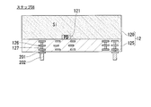
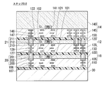
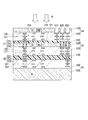
- FIG. 1 shows a configuration example of a solid-state imaging device according to the present embodiment.
- FIG. 1 shows a cross section of the solid-state imaging device.
- the solid-state imaging device illustrated in FIG. 1 includes a plurality of stacked (stacked) substrates (the first substrate 10, the second substrate 12, the third substrate 14), the connection portions 20 and 21, and the support substrate 30. And resin layers 110, 130, and 150.
- the first substrate 10, the second substrate 12, and the third substrate 14 are back-illuminated solid-state imaging devices.
- the thickness and width of the portion constituting the solid-state imaging device shown in FIG. 1 do not necessarily follow the thickness and width shown in FIG.
- the thickness and the width of the portion constituting the solid-state imaging device shown in FIG. 1 may be arbitrary.
- the first substrate 10 has a semiconductor layer 100 and a wiring layer 105.
- the semiconductor layer 100 and the wiring layer 105 overlap in a direction substantially perpendicular to the main surface of each substrate (the widest surface of the plurality of surfaces constituting the surface of the substrate).
- the semiconductor layer 100 and the wiring layer 105 are in contact with each other.
- the semiconductor layer 100 includes a photoelectric conversion unit (PD) 101 that converts incident light into a signal.
- the semiconductor layer 100 is made of a material containing a semiconductor such as silicon (Si).
- the photoelectric conversion portion 101 is made of, for example, a semiconductor material having an impurity concentration different from that of the semiconductor material forming the semiconductor layer 100.
- the semiconductor layer 100 has a first surface in contact with the wiring layer 105, and a second surface exposed to the outside, which is opposite to the first surface. The light incident on the second surface of the semiconductor layer 100 travels in the semiconductor layer 100 and is incident on the photoelectric conversion portion 101.
- the wiring layer 105 has a wiring 106 and a via 107.
- the wiring 106 transmits the signal generated by the photoelectric conversion unit 101 and other signals.
- the vias 107 connect the wirings 106 in different layers. Although a plurality of wires 106 exist in FIG. 1, the symbol of one wire 106 is shown as a representative. Further, although a plurality of vias 107 are present in FIG. 1, the symbol of one via 107 is shown as a representative.
- the wiring 106 is made of a conductive material (for example, a metal such as aluminum (Al) or copper (Cu)). Wiring layer 105 has a first surface in contact with resin layer 110 and a second surface opposite to the first surface and in contact with semiconductor layer 100.
- the wiring 106 is a thin film in which a wiring pattern is formed.
- the wiring 106 of only one layer may be formed, or the wirings 106 of a plurality of layers may be formed. In the example shown in FIG. 1, the wiring 106 of three layers is formed.
- the wires 106 in different layers are connected by vias 107.
- the vias 107 are made of a conductive material.
- portions other than the wiring 106 and the via 107 are made of, for example, an interlayer insulating film.
- the second substrate 12 has a semiconductor layer 120 and a wiring layer 125.
- the semiconductor layer 120 and the wiring layer 125 overlap in the direction substantially perpendicular to the main surface of each substrate.
- the semiconductor layer 120 and the wiring layer 125 are in contact with each other.
- the semiconductor layer 120 includes the photoelectric conversion unit 121. Since the semiconductor layer 120 is substantially the same as the semiconductor layer 100, the detailed description of the semiconductor layer 120 is omitted.
- the wiring layer 125 includes the wiring 126 and the via 127. Although a plurality of wires 126 exist in FIG. 1, the symbol of one wire 126 is shown as a representative. Further, although a plurality of vias 127 exist in FIG. 1, the symbol of one via 127 is shown as a representative. Since the wiring layer 125 is substantially the same as the wiring layer 105, the detailed description of the wiring layer 125 is omitted.
- the third substrate 14 has a semiconductor layer 140 and a wiring layer 145.
- the semiconductor layer 140 and the wiring layer 145 overlap in the direction substantially perpendicular to the main surface of each substrate.
- the semiconductor layer 140 and the wiring layer 145 are in contact with each other.
- the semiconductor layer 140 includes the photoelectric conversion unit 141.
- the semiconductor layer 140 is substantially the same as the semiconductor layer 100, and thus the detailed description of the semiconductor layer 140 is omitted.
- the wiring layer 145 has a wire 146 and a via 147. Although a plurality of wires 146 exist in FIG. 1, the symbol of one wire 146 is shown as a representative. Further, although a plurality of vias 147 exist in FIG. 1, the symbol of one via 147 is shown as a representative. Since the wiring layer 145 is substantially the same as the wiring layer 105, the detailed description of the wiring layer 145 is omitted.
- the support substrate 30 supports a plurality of substrates included in the solid-state imaging device.
- the support substrate 30 overlaps any one of a plurality of substrates included in the solid-state imaging device. In the example shown in FIG. 1, the support substrate 30 overlaps the first substrate 10.
- the support substrate 30 has a first surface exposed to the outside, and a second surface opposite to the first surface and in contact with the resin layer 110.
- the resin layers 110, 130, and 150 connect two adjacent substrates among a plurality of substrates included in the solid-state imaging device.
- the resin layers 110, 130, and 150 are made of, for example, epoxy resin.
- the resin layers 110, 130, 150 further increase the bonding strength between the substrates.
- the resin layer 110 is formed between the support substrate 30 and the first substrate 10.
- the support substrate 30 and the first substrate 10 are connected via the resin layer 110 in a state where the support substrate 30 and the wiring layer 105 of the first substrate 10 face each other.
- the resin layer 110 is in contact with the second surface of the support substrate 30 and the first surface of the wiring layer 105.
- the first substrate 10 is insulated from the support substrate 30 by the resin layer 110.
- the resin layer 130 is formed between the first substrate 10 and the second substrate 12.
- the first substrate 10 and the second substrate 12 are connected via the resin layer 130 in a state where the semiconductor layer 100 of the first substrate 10 and the wiring layer 125 of the second substrate 12 face each other.
- the resin layer 130 is in contact with the second surface of the semiconductor layer 100 and the first surface of the wiring layer 125.
- the second substrate 12 is insulated from the first substrate 10 by the resin layer 130.
- the resin layer 150 is formed between the second substrate 12 and the third substrate 14.
- the second substrate 12 and the third substrate 14 are connected via the resin layer 150 in a state where the semiconductor layer 120 of the second substrate 12 and the wiring layer 145 of the third substrate 14 face each other.
- the resin layer 150 is in contact with the second surface of the semiconductor layer 120 and the first surface of the wiring layer 145.
- the third substrate 14 is insulated from the second substrate 12 by the resin layer 150.
- connection portions 20 and 21 are disposed between two adjacent substrates, and electrically connect the two substrates. Although a plurality of connection parts 20 exist in FIG. 1, reference numerals of one connection part 20 are shown as a representative. In addition, although a plurality of connection portions 21 exist in FIG. 1, reference numerals of one connection portion 21 are shown as a representative.
- the connection portions 20 and 21 are made of a conductive material (for example, a metal such as gold (Au) or copper (Cu)).
- connection portion 20 electrically connects the first substrate 10 and the second substrate 12.
- the connection portion 20 includes connection electrodes 200 and 201 and a bump 202.
- the connection electrode 200 is formed in the wiring layer 105.
- the connection electrode 200 is connected to the wiring 106.
- An UBM (Under Barrier Metal) such as titanium (Ti) may be formed between the connection electrode 200 and the wiring 106.
- the connection electrode 201 is formed on the resin layer 130.
- the connection electrode 201 is connected to the wiring 126 through the via 127.
- a UBM such as titanium (Ti) may be formed between the connection electrode 201 and the via 127.
- the bumps 202 are connected to the connection electrodes 200 and 201. Since the bumps 202 are in contact with the connection electrodes 200 connected to the wiring 106, the bumps 202 are electrically connected to the wiring 106. In addition, since the bump 202 is in contact with the connection electrode 201 electrically connected to the wiring 126, the bump 202 is electrically connected to the wiring 126.
- the bumps 202 penetrate the semiconductor layer 100. Since the height of the bumps 202 is larger than the thickness of the semiconductor layer 100, the bumps 202 are formed across the semiconductor layer 100 and the resin layer 130.
- the bumps 202 electrically connect the wiring layer 105 (wiring 106) of the first substrate 10 and the wiring layer 125 (wiring 126) of the second substrate 12, and the semiconductor layer 100 of the first substrate 10.
- the wiring layer 125 of the second substrate 12 is a connection structure which penetrates only the semiconductor layer 100 of the first substrate 10.
- the periphery of the part passing through the semiconductor layer 100 is surrounded by the insulating layer 102.
- the insulating layer 102 is made of an insulating material (eg, silicon dioxide (SiO 2 )).
- the bump 202 is insulated from the semiconductor layer 100 by the insulating layer 102.
- connection portion 21 electrically connects the second substrate 12 and the third substrate 14.
- the connection portion 21 includes connection electrodes 210 and 211 and a bump 212.
- the connection electrode 210 is formed in the wiring layer 125.
- the connection electrode 210 is connected to the wiring 126.
- a UBM such as titanium (Ti) may be formed between the connection electrode 210 and the wiring 126.
- the connection electrode 211 is formed on the resin layer 150.
- the connection electrode 211 is connected to the wiring 146 through the via 147.
- a UBM such as titanium (Ti) may be formed between the connection electrode 211 and the via 147.
- the bumps 212 are connected to the connection electrodes 210 and 211.
- the bump 212 is in contact with the connection electrode 210 connected to the wiring 126, and thus is electrically connected to the wiring 126. Further, since the bumps 212 are in contact with the connection electrodes 211 electrically connected to the wirings 146, the bumps 212 are electrically connected to the wirings 146.
- the bumps 212 penetrate the semiconductor layer 120. Since the height of the bumps 212 is larger than the thickness of the semiconductor layer 120, the bumps 212 are formed across the semiconductor layer 120 and the resin layer 150.
- the bumps 212 electrically connect the wiring layer 125 (wiring 126) of the second substrate 12 and the wiring layer 145 (wiring 146) of the third substrate 14, and the semiconductor layer 120 of the second substrate 12.
- the wiring layer 145 of the third substrate 14 is a connection structure which penetrates only the semiconductor layer 120 of the second substrate 12.
- the periphery of the part penetrating the semiconductor layer 120 is surrounded by the insulating layer 122.
- the insulating layer 122 is made of an insulating material (eg, silicon dioxide (SiO 2 )).
- the bump 212 is insulated from the semiconductor layer 120 by the insulating layer 122.
- Grooves 400, 410, 420, 430 are formed in the semiconductor layer 140 and the wiring layer 145. At the bottom of the grooves 400, 410, 420 and 430, a part of the wiring 146 is exposed to the outside.
- the thickness of the semiconductor layer 140 is, for example, 10 ⁇ m or less, and the width of the grooves 400, 410, 420, 430 is, for example, 50 to 100 ⁇ m.
- a conductive wire can be connected to the wiring 146 from the outside by wire bonding.
- the wiring 146 exposed at the position where the grooves 400, 410, 420, and 430 are formed is an electrode for outputting a signal from the solid-state imaging device to the outside or applying an external signal to the solid-state imaging device.
- the third substrate 14 is the substrate disposed at the outermost side among the plurality of substrates in which the photoelectric conversion portions are formed, and the semiconductor layer 140 is more than the wiring layer 145. It is located outside.
- the third substrate 14 is electrically connected to the wiring layer 145 of the third substrate 14 and has an electrode (wiring 146) exposed to the outside.
- the outermost substrate among the plurality of substrates is a substrate having a main surface not in contact with another substrate among the plurality of substrates.
- the first substrate 10 and the third substrate 14 are the substrates disposed at the outermost side.
- the two substrates are the substrates disposed at the outermost side.
- the outermost one of the plurality of substrates is a plurality of substrates when the plurality of substrates are disposed such that at least one of the principal surfaces of the plurality of substrates is substantially parallel to the horizontal plane.
- the substrate disposed at the uppermost or lowermost side is disposed at the uppermost or lowermost side.
- the electrode at the position where the groove 400 is formed is used, for example, for common power supply, ground (GND), or clock in each substrate.
- the electrodes at the locations where the grooves 410, 420, 430 are formed are used, for example, for individual signals at each substrate.
- the individual signals in each substrate are, for example, signals output from the photoelectric conversion units 101, 121, 141, a clock for driving a circuit disposed in each substrate, or control supplied to a circuit disposed in each substrate It is a signal. In the case of outputting signals from the photoelectric conversion units 101, 121, and 141 to the outside at different speeds for each substrate, different clocks may be supplied for each substrate.
- the electrode at the position where the groove 410 is formed is used for the individual signal of the third substrate 14.
- the electrode at the position where the groove 420 is formed is used for the individual signal of the second substrate 12.
- the electrode at the position where the groove 430 is formed is used for individual signals of the first substrate 10.
- the signal output from the photoelectric conversion unit 101 is transferred to the second substrate 12 via the connection unit 20 at the position where the groove 430 is formed.
- the signal transferred to the second substrate 12 is transferred to the third substrate 14 via the connection 21.
- the signal transferred to the third substrate 14 is output to the outside from the electrode at the position where the groove 430 is formed.
- the signal output from the photoelectric conversion unit 121 is transferred to the third substrate 14 through the connection unit 21 at the position where the groove 420 is formed.
- the signal transferred to the third substrate 14 is output to the outside from the electrode at the position where the groove 420 is formed.
- a signal output from the photoelectric conversion unit 141 is output to the outside from an electrode at a position where the groove 410 is formed.
- the solid-state imaging device shown in FIG. 1 has three substrates on which the photoelectric conversion units are formed, but the solid-state imaging device has two substrates or four or more substrates on which the photoelectric conversion units are formed. You may have. Further, in the solid-state imaging device shown in FIG. 1, the adjacent substrates are connected by the resin layers 110, 130, and 150, but the method of connecting the adjacent substrates is not limited thereto. Further, an electrode of metal or the like connected to the wiring 146 may be formed at the bottom of the groove 400, 410, 420, 430.
- the structure not necessarily directly related to the structure (for example, the photoelectric conversion units 101, 121, and 141) essential to the solid-state imaging device, or the structure not necessarily directly related to the connection units 20 and 21 It is not a characteristic structure of the solid-state imaging device according to the present embodiment. That is, the support substrate 30, the insulating layers 102, 122, the resin layers 110, 130, 150, the vias 107, 127, 147, and the grooves 400, 410, 420, 430 correspond to those of the solid-state imaging device according to the present embodiment. It is not a distinctive structure. In addition, these structures are not essential for obtaining the characteristic effects of the solid-state imaging device according to the present embodiment.
- connection electrodes 200 and 201 of the connection portion 20 have an auxiliary structure for connecting the bump 202 to the wiring layer 105 and the wiring layer 125, the characteristic effect of the solid-state imaging device according to the present embodiment is obtained. It is not a required structure for The same applies to the connection electrodes 210 and 211 of the connection portion 21.
- the bumps 202 penetrate only the semiconductor layer 100, and the bumps 212 penetrate only the semiconductor layer 120. Therefore, the bumps 202 and 212 can be more easily manufactured as compared to the case of forming a through electrode penetrating one or more substrates. That is, it is possible to provide a solid-state imaging device that is easier to manufacture.
- connection electrodes 910, 911, 912 formed on each substrate are used.
- the through electrodes need to be formed to penetrate the However, it is difficult to form through electrodes so as to penetrate connection electrodes 910, 911, and 912 formed of metal. For this reason, it is necessary to separately provide the through electrodes 900, 901, 902 without making them common. In this case, it is difficult to miniaturize the solid-state imaging device because the through electrodes 900, 901, and 902 need to be provided separately.
- the solid-state imaging device shown in FIG. 1 it is not necessary to prepare a plurality of structures corresponding to each substrate for a power supply common to the plurality of substrates.
- power is supplied to the third substrate 14 by externally supplying power to the wiring layer 145.
- the power applied to the interconnection layer 145 is simultaneously applied to the interconnection layer 125 via the bumps 212.
- power is supplied to the second substrate 12.
- the power supplied to the wiring layer 125 is simultaneously supplied to the wiring layer 105 through the bumps 202. Power is thereby supplied to the first substrate 10.
- the solid-state imaging device can be miniaturized.
- the bumps 202 and 212 contribute to the miniaturization of the solid-state imaging device. For this reason, it is possible to provide a solid-state imaging device that is miniaturized and easier to manufacture.
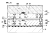
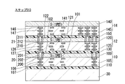
- 2A to 8B show an example of a procedure for manufacturing a solid-state imaging device.
- 2A-8B show cross sections of the solid-state imaging device.
- Step S0 A first substrate 10 having a semiconductor layer 100 and a wiring layer 105 is prepared.
- the photoelectric conversion unit 101 is formed in the semiconductor layer 100.
- the wiring 106 is formed in the wiring layer 105 and overlaps with the semiconductor layer 100.
- the second substrate 12 having the semiconductor layer 120 and the wiring layer 125 is prepared in the semiconductor layer 120.
- the photoelectric conversion unit 121 is formed in the semiconductor layer 120.
- the wiring 126 is formed in the wiring layer 125 and overlaps with the semiconductor layer 120.
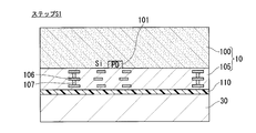
- Step S1 The first surface of the wiring layer 105 is connected to the support substrate 30 via the resin layer 110. Thereby, the first substrate 10 is bonded to the support substrate 30 via the resin layer 110 (FIG. 2A).
- Step S2 The second surface of the semiconductor layer 100 is polished. As a result, the semiconductor layer 100 becomes thinner (FIG. 2B).
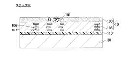
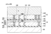
- Step S3 A part of the semiconductor layer 100 is etched from the second surface side, and the groove 103 is formed in the semiconductor layer 100. At this time, etching is performed so as to penetrate the semiconductor layer 100 and expose the wiring layer 105. In the example of the present embodiment, the etching is performed until the wiring 106 of the wiring layer 105 is exposed (FIG. 3A).
- Step S3 is a step of etching a part of the semiconductor layer 100 of the first substrate 10 having the semiconductor layer 100 and the wiring layer 105 to expose the wiring layer 105 of the first substrate 10.
- the photoelectric conversion unit 101 is formed in the semiconductor layer 100.
- the wiring 106 is formed in the wiring layer 105 and overlaps with the semiconductor layer 100.
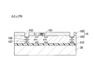
- connection electrode 200 is formed on the surface of the wiring 106 exposed by the etching. Further, the insulating layer 102 is formed on the surface of the groove 103 (FIG. 3B).
- connection electrode 201 is formed at the position where the via 127 is exposed. Thus, the connection electrode 201 is electrically connected to the via 127. Further, since the connection electrode 201 is in contact with the via 127 connected to the wiring 126, the connection electrode 201 is electrically connected to the wiring 126 (FIG. 4A).
- Step S6 A bump 202 connected to the connection electrode 201 is formed.
- the bumps 202 formed are in contact with the connection electrodes 201 electrically connected to the wirings 126, and thus are electrically connected to the wirings 126 (FIG. 4B).
- the height of the bumps 202 is preferably larger than the thickness of the semiconductor layer 100.
- Step S6 is a step of forming a connection structure electrically connected to the wiring layer 125 (wiring 126) of the second substrate 12 having the semiconductor layer 120 and the wiring layer 125.
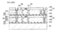
- Step S7 In a state where the semiconductor layer 100 of the first substrate 10 and the wiring layer 125 of the second substrate 12 face each other, connection is made with the support substrate 30 so that the planar positions of the bumps 202 and the connection electrodes 200 substantially coincide. The positions of the first substrate 10 and the second substrate 12 are adjusted. Subsequently, the bumps 202 are inserted into the grooves covered with the insulating layer 102 and connected to the connection electrodes 200. As a result, the wiring layer 105 and the wiring layer 125 are electrically connected by the connection portion 20 having the connection electrodes 200 and 201 and the bumps 202, and the first substrate 10 and the second substrate 12 are joined. Be done.
- the bumps 202 are in contact with the connection electrodes 200 connected to the wiring 106 and thus are electrically connected to the wiring 106. Further, in the state where the first substrate 10 and the second substrate 12 are joined, a gap exists between the first substrate 10 and the second substrate 12 (FIG. 5A).
- the connection between the bump 202 and the connection electrode 200 is performed as follows. For example, in a state in which the semiconductor layer 100 and the wiring layer 125 face each other, the first substrate 10 and the second substrate 12 bonded to the support substrate 30 are sandwiched by the pressure plate. When heated and pressed by the pressing device in this state, the bumps 202 and the connection electrodes 200 are electrically bonded. Before the bumps 202 and the connection electrodes 200 are joined, the surface of the first substrate 10, the surface of the second substrate 12, the connection electrodes 200 and 201, and the bumps 202 are subjected to plasma cleaning, reverse sputtering, or the like. It may be cleaned. By so-called surface activation, the bumps 202 and the connection electrodes 200 can be easily joined.
- Step S7 etches the bump 202 which is a connection structure in a state where the semiconductor layer 100 of the first substrate 10 and the wiring layer 125 of the second substrate 12 face each other. And the wiring layer 105 (wiring 106) of the first substrate 10 exposed by the above process.
- Step S8 A resin is filled between the first substrate 10 and the second substrate 12 to form a resin layer 130 (FIG. 5B).
- the formation of the resin layer 130 is performed as follows. For example, an epoxy resin which has been heated and becomes highly fluid is poured between the first substrate 10 and the second substrate 12. Thereafter, the poured epoxy resin is cooled and the epoxy resin is solidified. When an epoxy resin is poured between the first substrate 10 and the second substrate 12, a differential pressure effect may be used.
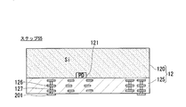
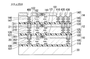
- Step S9 The second surface of the semiconductor layer 120 is polished. As a result, the semiconductor layer 120 becomes thinner (FIG. 6A).
- Step S10 A portion of the semiconductor layer 120 is etched from the second surface side, and a groove is formed in the semiconductor layer 120. At this time, etching is performed such that the semiconductor layer 120 is penetrated and the wiring layer 125 is exposed. In the example of the present embodiment, etching is performed until the wiring 126 of the wiring layer 125 is exposed.
- the connection electrode 210 is formed on the surface of the wiring 126 exposed by the etching.
- the insulating layer 122 is formed on the surface of the groove formed by the etching (FIG. 6B).
- Step S10 is a process corresponding to steps S3 and S4.
- connection electrode 211 is formed at a position where the via 147 is exposed on the first surface of the wiring layer 145 of the third substrate 14. Thus, the connection electrode 211 is electrically connected to the via 147. Further, since the connection electrode 211 is in contact with the via 147 connected to the wiring 146, the connection electrode 211 is electrically connected to the wiring 146. Furthermore, bumps 212 connected to the connection electrodes 211 are formed. The bumps 212 formed are in contact with the connection electrodes 211 electrically connected to the wirings 146, and thus are electrically connected to the wirings 146 (FIG. 7A). The height of the bumps 212 is preferably greater than the thickness of the semiconductor layer 120. Step S11 is a process corresponding to steps S5 and S6.
- Step S12 In a state where the semiconductor layer 120 of the second substrate 12 and the wiring layer 145 of the third substrate 14 face each other, the second substrate 12 so that the planar positions of the bumps 212 and the connection electrodes 210 substantially coincide with each other. And the position of the third substrate 14 are adjusted. Subsequently, the bumps 212 are inserted into the grooves covered with the insulating layer 122 and connected to the connection electrodes 210. Thus, the wiring layer 125 and the wiring layer 145 are electrically connected by the connection portion 21 having the connection electrodes 210 and 211 and the bumps 212, and the second substrate 12 and the third substrate 14 are joined. Be done.
- Step S12 is a process corresponding to steps S7 and S8.
- Step S13 The second surface of the semiconductor layer 140 is polished. As a result, the semiconductor layer 140 becomes thinner (FIG. 8A).
- Step S14 A part of the semiconductor layer 140 is etched from the second surface side, and the trenches 400, 410, 420, 430 are formed in the semiconductor layer 140. At this time, etching is performed to penetrate the semiconductor layer 140 and to expose the wiring layer 145. In the example of the present embodiment, etching is performed until the wiring 146 of the wiring layer 145 is exposed. Thus, an electrode electrically connected to the outside is formed (FIG. 8B).
- steps S0 to S2, S8 to S9, and S13 to S14 are not characteristic steps of the method for manufacturing a solid-state imaging device according to the present embodiment.
- steps S0 to S2, S8 to S9, and S13 to S14 are not characteristic steps of the method for manufacturing a solid-state imaging device according to the present embodiment.
- the step of forming the insulating layer 102 in step S4 and the step of forming the resin layer 150 in step S12 are not characteristic steps of the method of manufacturing a solid-state imaging device according to the present embodiment.
- these steps are not essential steps to obtain the characteristic effects of the method of manufacturing a solid-state imaging device according to the present embodiment.
- step of forming the connection electrode 200 in step S4 and the step of forming the connection electrode 201 in step S5 are auxiliary steps for connecting the bump 202 to the semiconductor layer 100 and the wiring layer 125, It is not an essential step to obtain the characteristic effects of the method for manufacturing a solid-state imaging device according to the present embodiment.
- the bumps 202 penetrate only the semiconductor layer 100, and the bumps 212 penetrate only the semiconductor layer 120. Therefore, the bumps 202 and 212 can be more easily manufactured as compared to the case of forming a through electrode penetrating one or more substrates. That is, the solid-state imaging device can be manufactured more easily.
- the plurality of overlapping substrates (the first substrate 10, the second substrate 12, the third substrate 14), each of the plurality of substrates converts incident light into a signal
- connection structure (bump 202 or bump 212) (step S6 or step S11), and the semiconductor layer 100 (or the second substrate) of the first substrate 10
- the connection structure (bump 202 or bump 212) is Electrically connect with the wiring layer 105 (or the wiring layer 125 of the second substrate 12) of the first substrate 10 exposed by etching the semiconductor layer 100 of the substrate 10 (or the semiconductor layer 120 of the second substrate 12) And a step (step S7 or step S12).
- the wiring layer 105 of the first substrate 10 or the second substrate 12 is formed by the bumps 202 or the bumps 212 penetrating only the semiconductor layer 100 of the first substrate 10 or the semiconductor layer 120 of the second substrate 12.
- the wiring layer 125 and the wiring layer 125 of the second substrate 12 or the wiring layer 145 of the third substrate 14 are electrically connected to each other, so that manufacturing of the solid-state imaging device can be made easier. In addition, the manufacture of a miniaturized solid-state imaging device can be made easier.
- FIG. 9 shows a configuration example of the solid-state imaging device according to the present embodiment.
- FIG. 9 shows a cross section of the solid-state imaging device.
- the insulating layer 102 in the solid-state imaging device shown in FIG. 1 is changed to the resin layer 131, and the insulating layer 122 is changed to the resin layer 151. That is, in the bump 202, the periphery of the part penetrating the semiconductor layer 100 is surrounded by the resin layer 131. Further, in the bump 212, the periphery of the part penetrating the semiconductor layer 120 is surrounded by the resin layer 151.
- the structure other than the resin layers 131 and 151 is substantially the same as the structure of the solid-state imaging device illustrated in FIG. 1, and thus the description of the structure other than the resin layers 131 and 151 is omitted.
- the resin layer 131 is made of the same resin as that of the resin layer 130. Further, the resin layer 151 is made of the same resin as the resin forming the resin layer 150.
- the process of forming the insulating layers 102 and 122 in 1st Embodiment is unnecessary.
- the resin layer 131 is formed in the step of forming the resin layer 130
- the resin layer 151 is formed in the step of forming the resin layer 150.
- the solid-state imaging device can be manufactured with fewer steps.
- FIG. 10 shows a configuration example of the solid-state imaging device according to the present embodiment.
- FIG. 10 shows a cross section of the solid-state imaging device.
- the first substrate 10, the resin layer 110, and the support substrate 30 in the solid-state imaging device shown in FIG. 9 are changed to the support substrate 31, and the connection portion 20 is changed to the connection portion 22. It is done. Further, in the solid-state imaging device shown in FIG. 10, the groove 400 in the solid-state imaging device shown in FIG. 9 is eliminated.
- the structure other than the above-described structure is substantially the same as the structure of the solid-state imaging device shown in FIG.
- the resin layer 151 in FIG. 10 may be changed to the insulating layer 122 in FIG.
- the support substrate 31 overlaps the second substrate 12 disposed at the outermost side among the plurality of substrates in which the photoelectric conversion units are formed. More specifically, the support substrate 31 is a substrate disposed at the outermost side among the plurality of substrates in which the photoelectric conversion units are formed, and the second wiring layer 125 is disposed at the outer side than the semiconductor layer 120. And the substrate 12 of FIG.
- the support substrate 31 has a wiring layer 310 and a circuit board 315.
- the wiring layer 310 and the circuit board 315 overlap in the direction perpendicular to the main surface of each substrate.
- the wiring layer 310 and the circuit board 315 are in contact with each other.
- the wiring layer 310 has a wiring 311 and a via 312.
- the wiring 311 transmits signals generated by the photoelectric conversion units 121 and 141 and other signals.
- the vias 312 connect the wirings 311 in different layers. Although a plurality of wires 311 exist in FIG. 10, the symbol of one wire 311 is shown as a representative. Further, although a plurality of vias 312 exist in FIG. 10, the symbol of one via 312 is shown as a representative.
- the wiring 311 is made of a conductive material (for example, a metal such as aluminum (Al) or copper (Cu)).
- Wiring layer 310 has a first surface in contact with circuit board 315 and a second surface opposite to the first surface and in contact with resin layer 130.
- the wiring 311 is a thin film in which a wiring pattern is formed.
- the wiring 311 of only one layer may be formed, or the wirings 311 of a plurality of layers may be formed. In the example illustrated in FIG. 10, the wirings 311 in three layers are formed.
- the wires 311 in different layers are connected by vias 312.
- the vias 312 are made of a conductive material.
- portions other than the wiring 311 and the via 312 are made of, for example, an interlayer insulating film.
- the circuit board 315 is made of a material containing a semiconductor such as silicon (Si). Circuit board 315 has a first surface exposed to the outside, and a second surface opposite to the first surface and in contact with wiring layer 310.
- the circuit board 315 includes a processing circuit (for example, an amplifier circuit) that processes a signal generated by the photoelectric conversion unit 121 or 141 formed on any of a plurality of substrates.
- the circuit substrate 315 may be a driver circuit that drives a pixel including the photoelectric conversion unit 121 or 141 formed on any of a plurality of substrates (for example, a reset circuit that resets the photoelectric conversion unit 121 or 141, or a photoelectric conversion unit And a transfer circuit for transferring the charges accumulated in 121 and 141 to the charge storage portion.
- the processing circuit or drive circuit may be formed in the wiring layer 310.
- connection portion 22 is disposed between the adjacent support substrate 31 and the second substrate 12 and electrically connects the support substrate 31 and the second substrate 12.
- a plurality of connection parts 22 exist, but the symbol of one connection part 22 is shown as a representative.
- the connection portion 22 is made of a conductive material (for example, a metal such as gold (Au) or copper (Cu)).
- connection portion 22 includes connection electrodes 220 and 221 and a bump 222.
- the connection portion 22 is formed in the resin layer 130.
- the connection electrode 220 is connected to the wiring 311 through the via 312.
- a UBM such as titanium (Ti) may be formed between the connection electrode 220 and the via 312.
- the connection electrode 221 is connected to the wiring 126 through the via 127.
- a UBM such as titanium (Ti) may be formed between the connection electrode 221 and the via 127.
- the bumps 222 are connected to the connection electrodes 220 and 221. Since the bumps 222 are in contact with the connection electrodes 220 connected to the wiring 311, the bumps 222 are electrically connected to the wiring 311. Further, since the bumps 222 are in contact with the connection electrodes 221 electrically connected to the wirings 126, the bumps 222 are electrically connected to the wirings 126.
- the bump 222 electrically connects the wiring layer 310 (wiring 311) of the support substrate 31 and the wiring layer 125 (wiring 126) of the second substrate 12 by connecting the connection electrode 220 and the connection electrode 221. .
- the structure for connecting the second substrate 12 and the third substrate 14 in the solid-state imaging device shown in FIG. 10 is the structure for connecting the first substrate 10 and the second substrate 12 in the solid-state imaging device shown in FIG. It is almost the same as Therefore, it is possible to provide a solid-state imaging device that is easier to manufacture.
- a supporting substrate 31 is used instead of the first substrate 10, the resin layer 110, and the supporting substrate 30 in the procedure for manufacturing the solid-state imaging device shown in FIG. Instead of the connection portion 20, the connection portion 22 is formed.
- the other procedures are almost the same as the procedures for manufacturing the solid-state imaging device shown in FIG. 1, and thus the description of the procedures for manufacturing the solid-state imaging device shown in FIG. 10 will be omitted.
- the signal output from the photoelectric conversion unit 121 is transferred to the support substrate 31 via the connection unit 22 located on the left side of the photoelectric conversion units 121 and 141.
- the signal transferred to the support substrate 31 is processed by the processing circuit formed on the circuit board 315.
- the signal processed by the processing circuit is transferred to the second substrate 12 via the connection 22 at the position where the groove 430 is formed.
- the signal transferred to the second substrate 12 is transferred to the third substrate 14 via the connection 21.
- the signal transferred to the third substrate 14 is output to the outside from the electrode at the position where the groove 430 is formed.
- the signal output from the photoelectric conversion unit 141 is transferred to the second substrate 12 through the connection unit 21 located on the left side of the photoelectric conversion units 121 and 141.
- the signal transferred to the second substrate 12 is transferred to the support substrate 31 via the connection portion 22.
- the signal transferred to the support substrate 31 is processed by the processing circuit formed on the circuit board 315.
- the signal processed by the processing circuit is output to the outside from the electrode at the position where the groove 430 is formed, as described above.
- the signal output from the photoelectric conversion unit 121 and the signal output from the photoelectric conversion unit 141 may be transferred from the second substrate 12 to the support substrate 31 via different connection units 22.
- signals may be output from the photoelectric conversion unit 121 and the photoelectric conversion unit 141 in a time division manner, and the signals may be transferred from the second substrate 12 to the support substrate 31 through the same connection unit 22.
- the signals output from the photoelectric conversion units 121 and 141 and processed by the processing circuit may be transferred from the support substrate 31 to the third substrate 14 via different connection units 21 and 22.
- the signal output from the photoelectric conversion unit 121 and processed by the processing circuit and the signal output from the photoelectric conversion unit 141 and processed by the processing circuit are output from the processing circuit in time division, and the signals are identical.
- the transfer from the support substrate 31 to the third substrate 14 may be performed via the connection portions 21 and 22 of FIG.
- the transfer path of the drive signal output from the drive circuit that drives the pixels including the photoelectric conversion units 121 and 141 will be described below.
- a drive signal is transferred through the connection units 21 and 22 located on the left side of the photoelectric conversion units 121 and 141 will be described.
- the drive signal output from the drive circuit is transferred to the second substrate 12 via the connection portion 22.
- the drive signal transferred to the second substrate 12 is transferred to each circuit of the pixel including the photoelectric conversion unit 121 through the wiring 126 and the via 127.
- the drive signal transferred to the second substrate 12 is transferred to the third substrate 14 via the connection portion 21.
- the drive signal transferred to the third substrate 14 is transferred to each circuit of the pixel including the photoelectric conversion unit 141 through the wiring 146 and the via 147.
- the substrate on which the photoelectric conversion unit is formed may not be provided with the processing circuit or the drive circuit.
- part of the processing circuit or the driver circuit which is provided over the substrate on which the photoelectric conversion portion is formed can be moved to the supporting substrate 31. Therefore, the size of the solid-state imaging device can be further reduced as compared with the case where the processing circuit or the drive circuit is provided on the substrate on which the photoelectric conversion unit is formed.
- the processing circuit can be added to the support substrate 31, more functions can be mounted on the solid-state imaging device.
- FIG. 11 shows a configuration example of the solid-state imaging device according to the present embodiment.
- FIG. 11 shows a cross section of the solid-state imaging device.
- the structure of the electrodes in the solid-state imaging device shown in FIG. 10 is changed to a different structure.
- the structure other than the structure of the electrode is substantially the same as the structure of the solid-state imaging device shown in FIG.
- Electrodes 40, 41, 42, and 43 are formed on the first surface of the circuit board 315 opposite to the second surface in contact with the wiring layer 310.
- the electrodes 40, 41, 42 and 43 are made of a conductive material.
- the electrode 40 and the wiring 311 are connected by a through electrode 440 penetrating the circuit board 315.
- the electrode 41 and the wiring 311 are connected by a through electrode 441 penetrating the circuit board 315.
- the electrode 42 and the wiring 311 are connected by a through electrode 442 which penetrates the circuit board 315.
- the electrode 43 and the wiring 311 are connected by a through electrode 443 penetrating the circuit board 315.
- the through electrodes 440, 441, 442, 443 are made of a conductive material.
- the solid-state imaging device illustrated in FIG. 11 includes the support substrate 31 overlapping the second substrate 12 disposed outermost among the plurality of substrates in which the photoelectric conversion units are formed. More specifically, the solid-state imaging device shown in FIG. 11 is the outermost substrate of the plurality of substrates on which the photoelectric conversion units are formed, and the wiring layer 125 is disposed outside the semiconductor layer 120. And a supporting substrate 31 overlapping the second substrate 12. The support substrate 31 is electrically connected to the wiring layer 125 of the second substrate 12 overlapping the support substrate 31 among the plurality of substrates in which the photoelectric conversion units are formed, and the electrodes 40, 41, 42, and 43 exposed to the outside Have.
- the electrodes 40 are used, for example, for common power supply, ground (GND), or clock in each substrate.
- the electrodes 41, 42, 43 are used, for example, for individual signals of each substrate.
- the signal output from the photoelectric conversion unit 121 is transferred to the support substrate 31 via the connection unit 22 at the position where the electrode 42 is formed.
- the signal transferred to the support substrate 31 is transferred to the electrode 42 through the through electrode 442.
- the signal transferred to the electrode 42 is output from the electrode 42 to the outside.
- the signal output from the photoelectric conversion unit 141 is transferred to the second substrate 12 via the connection unit 21 at the position where the electrode 43 is formed.
- the signal transferred to the second substrate 12 is transferred to the support substrate 31 via the connection portion 22.
- the signal transferred to the support substrate 31 is transferred to the electrode 43 via the through electrode 443.
- the signal transferred to the electrode 43 is output from the electrode 43 to the outside.
- a support substrate 31 is used instead of the first substrate 10, the resin layer 110, and the support substrate 30 in the procedure for manufacturing the solid-state imaging device shown in FIG. Instead of the connection portion 20, the connection portion 22 is formed.
- the connection portion 22 is formed.
- the first surface of the circuit board 315 is polished, and after the circuit board 315 is thinned, a groove penetrating the circuit board 315 is formed. Be done. By burying metal in the groove, the electrodes 40, 41, 42, 43 and the through electrodes 440, 441, 442, 443 are formed.
- the other procedures are almost the same as the procedures for manufacturing the solid-state imaging device shown in FIG. 1, and thus the description of the procedures for manufacturing the solid-state imaging device shown in FIG. 11 will be omitted.
- the electrodes 40, 41, 42 and 43 and the through electrodes 440, 441, 442 and 443 are formed on the support substrate 31, but the support substrate 30 of the solid-state imaging device shown in FIG.
- the electrodes 40, 41, 42 and 43 and the through electrodes 440, 441, 442 and 443 may be formed.
- the electrodes 40, 41, 42 and 43 are formed on the support substrate 31. For this reason, when forming a package including a solid-state imaging device, it becomes possible to connect the electrodes 40, 41, 42 and 43 and the substrate on which the package is mounted by soldering or the like. When forming a package by providing an electrode on the surface of the third substrate 14 and connecting a wire to the electrode from the outside by wire bonding, a lead connected to the wire is required, and the area of the package is increased. Therefore, in the present embodiment, the area of the package can be further reduced.
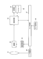
- FIG. 12 shows a configuration example of an imaging device according to the present embodiment.
- the imaging device according to the present embodiment may be any electronic device having an imaging function, and may be a digital video camera, an endoscope or the like besides a digital camera.
- the imaging apparatus shown in FIG. 12 includes a lens 51, an imaging unit 52, an image processing unit 53, a display unit 54, a drive control unit 55, a lens control unit 56, a camera control unit 57, and a camera operation unit 58. And.
- a memory card 59 is also shown in FIG. 12, the memory card 59 may be configured to be removable from the imaging apparatus. That is, the memory card 59 may not have a configuration unique to the imaging device.
- the lens 51 is a photographing lens for forming an optical image of a subject on an imaging surface of an imaging unit 52 constituting a solid-state imaging device.
- the imaging unit 52 converts an optical image of an object formed by the lens 51 into a digital image signal by photoelectric conversion and outputs the digital image signal.
- the imaging unit 52 is any of the solid-state imaging devices according to the first to fourth embodiments.
- the image processing unit 53 performs various digital image processing on the image signal output from the imaging unit 52.
- the display unit 54 displays an image based on the image signal subjected to image processing by the image processing unit 53 for display.
- the display unit 54 can display a still image and can perform moving image (live view) display for displaying an image of an imaging range in real time.
- the drive control unit 55 controls the operation of the imaging unit 52 based on an instruction from the camera control unit 57.
- the lens control unit 56 controls the aperture and the focal position of the lens 51 based on an instruction from the camera control unit 57.
- the camera control unit 57 controls the entire imaging apparatus.
- the operation of the camera control unit 57 is defined by a program stored in a ROM incorporated in the imaging device.
- the camera control unit 57 reads this program and performs various controls in accordance with the contents defined by the program.
- the camera operation unit 58 includes various members for operation for the user to perform various operation inputs to the imaging device, and outputs a signal based on the result of the operation input to the camera control unit 57.
- a power switch for turning on / off the power of the imaging apparatus a release button for instructing still image shooting, and a still image shooting mode between single shooting mode and continuous shooting mode
- the memory card 59 is a recording medium for storing the image signal processed for recording by the image processing unit 53.
- any one of the solid-state imaging devices according to the first to fourth embodiments is used in the imaging unit 52. For this reason, an imaging device can be manufactured more easily.
- connection structure that penetrates only the semiconductor layer of the first substrate electrically connects the wiring layer of the first substrate and the wiring layer of the second substrate, so the size is reduced. Also, it is possible to provide a solid-state imaging device and a method of manufacturing the solid-state imaging device, which are easier to manufacture.
Landscapes
- Engineering & Computer Science (AREA)
- Microelectronics & Electronic Packaging (AREA)
- Power Engineering (AREA)
- Physics & Mathematics (AREA)
- Condensed Matter Physics & Semiconductors (AREA)
- General Physics & Mathematics (AREA)
- Computer Hardware Design (AREA)
- Multimedia (AREA)
- Signal Processing (AREA)
- Manufacturing & Machinery (AREA)
- Solid State Image Pick-Up Elements (AREA)
- Transforming Light Signals Into Electric Signals (AREA)
Priority Applications (1)
| Application Number | Priority Date | Filing Date | Title |
|---|---|---|---|
| US15/149,955 US20160254299A1 (en) | 2013-12-10 | 2016-05-09 | Solid-state imaging device, imaging device, solid-state imaging device manufacturing method |
Applications Claiming Priority (2)
| Application Number | Priority Date | Filing Date | Title |
|---|---|---|---|
| JP2013-255423 | 2013-12-10 | ||
| JP2013255423A JP6177117B2 (ja) | 2013-12-10 | 2013-12-10 | 固体撮像装置、撮像装置、固体撮像装置の製造方法 |
Related Child Applications (1)
| Application Number | Title | Priority Date | Filing Date |
|---|---|---|---|
| US15/149,955 Continuation US20160254299A1 (en) | 2013-12-10 | 2016-05-09 | Solid-state imaging device, imaging device, solid-state imaging device manufacturing method |
Publications (1)
| Publication Number | Publication Date |
|---|---|
| WO2015087918A1 true WO2015087918A1 (ja) | 2015-06-18 |
Family
ID=53371219
Family Applications (1)
| Application Number | Title | Priority Date | Filing Date |
|---|---|---|---|
| PCT/JP2014/082696 Ceased WO2015087918A1 (ja) | 2013-12-10 | 2014-12-10 | 固体撮像装置、撮像装置、固体撮像装置の製造方法 |
Country Status (3)
| Country | Link |
|---|---|
| US (1) | US20160254299A1 (enExample) |
| JP (1) | JP6177117B2 (enExample) |
| WO (1) | WO2015087918A1 (enExample) |
Cited By (1)
| Publication number | Priority date | Publication date | Assignee | Title |
|---|---|---|---|---|
| US12027557B2 (en) | 2018-10-16 | 2024-07-02 | Sony Semiconductor Solutions Corporation | Semiconductor element and method of manufacturing the same |
Families Citing this family (12)
| Publication number | Priority date | Publication date | Assignee | Title |
|---|---|---|---|---|
| JP6439076B2 (ja) * | 2016-04-25 | 2018-12-19 | オリンパス株式会社 | 撮像素子、内視鏡および内視鏡システム |
| JP2018081946A (ja) * | 2016-11-14 | 2018-05-24 | ソニーセミコンダクタソリューションズ株式会社 | 固体撮像装置およびその製造方法、並びに電子機器 |
| WO2018154644A1 (ja) * | 2017-02-22 | 2018-08-30 | オリンパス株式会社 | 固体撮像装置、蛍光観察内視鏡装置、および固体撮像装置の製造方法 |
| JP6779825B2 (ja) | 2017-03-30 | 2020-11-04 | キヤノン株式会社 | 半導体装置および機器 |
| US11329077B2 (en) * | 2017-03-31 | 2022-05-10 | Sony Semiconductor Solutions Corporation | Semiconductor device with a through electrode reception part wider than a through electrode, solid-state imaging device, and electronic equipment |
| JP7128178B2 (ja) * | 2017-04-04 | 2022-08-30 | ソニーセミコンダクタソリューションズ株式会社 | 半導体装置、半導体装置の製造方法、及び電子機器 |
| WO2018186027A1 (ja) * | 2017-04-04 | 2018-10-11 | ソニーセミコンダクタソリューションズ株式会社 | 半導体装置、半導体装置の製造方法、及び電子機器 |
| WO2018186191A1 (ja) | 2017-04-04 | 2018-10-11 | ソニーセミコンダクタソリューションズ株式会社 | 固体撮像装置、及び電子機器 |
| US11411037B2 (en) * | 2017-04-04 | 2022-08-09 | Sony Semiconductor Solutions Corporation | Solid-state imaging device and electronic apparatus including coupling structures for electrically interconnecting stacked semiconductor substrates |
| US11276676B2 (en) * | 2018-05-15 | 2022-03-15 | Invensas Bonding Technologies, Inc. | Stacked devices and methods of fabrication |
| WO2020010265A1 (en) | 2018-07-06 | 2020-01-09 | Invensas Bonding Technologies, Inc. | Microelectronic assemblies |
| JP2022040579A (ja) * | 2020-08-31 | 2022-03-11 | ソニーセミコンダクタソリューションズ株式会社 | 半導体装置、および、半導体装置の製造方法 |
Citations (6)
| Publication number | Priority date | Publication date | Assignee | Title |
|---|---|---|---|---|
| JPH05267394A (ja) * | 1992-03-19 | 1993-10-15 | Sumitomo Electric Ind Ltd | 半導体素子の実装方法 |
| JP2001339057A (ja) * | 2000-05-30 | 2001-12-07 | Mitsumasa Koyanagi | 3次元画像処理装置の製造方法 |
| WO2007105478A1 (ja) * | 2006-02-27 | 2007-09-20 | Mitsumasa Koyanagi | 集積センサを搭載した積層型半導体装置 |
| WO2011148445A1 (ja) * | 2010-05-27 | 2011-12-01 | パナソニック株式会社 | 半導体装置及びその製造方法 |
| JP2011530165A (ja) * | 2008-08-01 | 2011-12-15 | オムニヴィジョン テクノロジーズ インコーポレイテッド | 複数のセンシング層を有するイメージセンサ |
| JP2013187475A (ja) * | 2012-03-09 | 2013-09-19 | Olympus Corp | 固体撮像装置およびカメラシステム |
Family Cites Families (5)
| Publication number | Priority date | Publication date | Assignee | Title |
|---|---|---|---|---|
| US7214999B2 (en) * | 2003-10-31 | 2007-05-08 | Motorola, Inc. | Integrated photoserver for CMOS imagers |
| JP2012033894A (ja) * | 2010-06-30 | 2012-02-16 | Canon Inc | 固体撮像装置 |
| JP5561190B2 (ja) * | 2011-01-31 | 2014-07-30 | 富士通株式会社 | 半導体装置、半導体装置の製造方法及び電子装置 |
| US20130075607A1 (en) * | 2011-09-22 | 2013-03-28 | Manoj Bikumandla | Image sensors having stacked photodetector arrays |
| TWI577001B (zh) * | 2011-10-04 | 2017-04-01 | Sony Corp | 固體攝像裝置、固體攝像裝置之製造方法及電子機器 |
-
2013
- 2013-12-10 JP JP2013255423A patent/JP6177117B2/ja not_active Expired - Fee Related
-
2014
- 2014-12-10 WO PCT/JP2014/082696 patent/WO2015087918A1/ja not_active Ceased
-
2016
- 2016-05-09 US US15/149,955 patent/US20160254299A1/en not_active Abandoned
Patent Citations (6)
| Publication number | Priority date | Publication date | Assignee | Title |
|---|---|---|---|---|
| JPH05267394A (ja) * | 1992-03-19 | 1993-10-15 | Sumitomo Electric Ind Ltd | 半導体素子の実装方法 |
| JP2001339057A (ja) * | 2000-05-30 | 2001-12-07 | Mitsumasa Koyanagi | 3次元画像処理装置の製造方法 |
| WO2007105478A1 (ja) * | 2006-02-27 | 2007-09-20 | Mitsumasa Koyanagi | 集積センサを搭載した積層型半導体装置 |
| JP2011530165A (ja) * | 2008-08-01 | 2011-12-15 | オムニヴィジョン テクノロジーズ インコーポレイテッド | 複数のセンシング層を有するイメージセンサ |
| WO2011148445A1 (ja) * | 2010-05-27 | 2011-12-01 | パナソニック株式会社 | 半導体装置及びその製造方法 |
| JP2013187475A (ja) * | 2012-03-09 | 2013-09-19 | Olympus Corp | 固体撮像装置およびカメラシステム |
Cited By (1)
| Publication number | Priority date | Publication date | Assignee | Title |
|---|---|---|---|---|
| US12027557B2 (en) | 2018-10-16 | 2024-07-02 | Sony Semiconductor Solutions Corporation | Semiconductor element and method of manufacturing the same |
Also Published As
| Publication number | Publication date |
|---|---|
| JP2015115420A (ja) | 2015-06-22 |
| JP6177117B2 (ja) | 2017-08-09 |
| US20160254299A1 (en) | 2016-09-01 |
Similar Documents
| Publication | Publication Date | Title |
|---|---|---|
| JP6177117B2 (ja) | 固体撮像装置、撮像装置、固体撮像装置の製造方法 | |
| US12125867B2 (en) | Imaging device and electronic device | |
| JP6779825B2 (ja) | 半導体装置および機器 | |
| KR102235927B1 (ko) | 반도체 장치 | |
| JP5970747B2 (ja) | 半導体装置 | |
| JP7158846B2 (ja) | 半導体装置および機器 | |
| KR20110107747A (ko) | 반도체 장치, 반도체 장치의 제조 방법, 반도체 장치의 설계 방법, 및 전자 기기 | |
| KR20110047133A (ko) | 반도체 장치와 그 제조 방법, 및 전자 기기 | |
| KR20120056204A (ko) | 고체 촬상 장치와 그 제조 방법, 및 전자 기기 | |
| JP2017130610A (ja) | イメージセンサ、製造方法、及び、電子機器 | |
| KR20100105380A (ko) | 반도체 장치와 그 제조 방법, 및 전자 기기 | |
| JP2020043265A (ja) | 光電変換装置および機器 | |
| WO2016152577A1 (ja) | 固体撮像装置および電子機器 | |
| JP2022031321A (ja) | 装置の製造方法、及び、装置 | |
| WO2017163953A1 (ja) | 半導体装置、固体撮像素子、撮像装置、および電子機器 | |
| WO2018047635A1 (ja) | 固体撮像素子および製造方法、並びに電子機器 | |
| JP6256562B2 (ja) | 固体撮像装置及び電子機器 | |
| WO2017126024A1 (ja) | 固体撮像装置および撮像装置 | |
| WO2014122999A1 (ja) | 積層型固体撮像装置および撮像装置 | |
| US20220157865A1 (en) | Semiconductor apparatus, imaging apparatus, and method of producing a semiconductor apparatus | |
| JP7282500B2 (ja) | 半導体装置、機器、半導体装置の製造方法 | |
| US9865641B2 (en) | Solid-state imaging device, manufacturing method therefor, and imaging apparatus | |
| JP2016034029A (ja) | 固体撮像装置 | |
| WO2017060948A1 (ja) | 固体撮像装置および撮像装置 | |
| WO2021090545A1 (ja) | 撮像素子および撮像装置 |
Legal Events
| Date | Code | Title | Description |
|---|---|---|---|
| 121 | Ep: the epo has been informed by wipo that ep was designated in this application |
Ref document number: 14869901 Country of ref document: EP Kind code of ref document: A1 |
|
| NENP | Non-entry into the national phase |
Ref country code: DE |
|
| 122 | Ep: pct application non-entry in european phase |
Ref document number: 14869901 Country of ref document: EP Kind code of ref document: A1 |