WO2015046292A1 - 電子部品収納用パッケージおよび電子装置 - Google Patents
電子部品収納用パッケージおよび電子装置 Download PDFInfo
- Publication number
- WO2015046292A1 WO2015046292A1 PCT/JP2014/075362 JP2014075362W WO2015046292A1 WO 2015046292 A1 WO2015046292 A1 WO 2015046292A1 JP 2014075362 W JP2014075362 W JP 2014075362W WO 2015046292 A1 WO2015046292 A1 WO 2015046292A1
- Authority
- WO
- WIPO (PCT)
- Prior art keywords
- side wall
- electronic component
- input
- output member
- storage package
- Prior art date
- Legal status (The legal status is an assumption and is not a legal conclusion. Google has not performed a legal analysis and makes no representation as to the accuracy of the status listed.)
- Ceased
Links
Images


Classifications
-
- H—ELECTRICITY
- H10—SEMICONDUCTOR DEVICES; ELECTRIC SOLID-STATE DEVICES NOT OTHERWISE PROVIDED FOR
- H10W—GENERIC PACKAGES, INTERCONNECTIONS, CONNECTORS OR OTHER CONSTRUCTIONAL DETAILS OF DEVICES COVERED BY CLASS H10
- H10W76/00—Containers; Fillings or auxiliary members therefor; Seals
- H10W76/10—Containers or parts thereof
- H10W76/12—Containers or parts thereof characterised by their shape
- H10W76/13—Containers comprising a conductive base serving as an interconnection
- H10W76/134—Containers comprising a conductive base serving as an interconnection having other interconnections parallel to the conductive base
-
- H—ELECTRICITY
- H01—ELECTRIC ELEMENTS
- H01G—CAPACITORS; CAPACITORS, RECTIFIERS, DETECTORS, SWITCHING DEVICES, LIGHT-SENSITIVE OR TEMPERATURE-SENSITIVE DEVICES OF THE ELECTROLYTIC TYPE
- H01G4/00—Fixed capacitors; Processes of their manufacture
- H01G4/002—Details
- H01G4/224—Housing; Encapsulation
-
- H—ELECTRICITY
- H01—ELECTRIC ELEMENTS
- H01S—DEVICES USING THE PROCESS OF LIGHT AMPLIFICATION BY STIMULATED EMISSION OF RADIATION [LASER] TO AMPLIFY OR GENERATE LIGHT; DEVICES USING STIMULATED EMISSION OF ELECTROMAGNETIC RADIATION IN WAVE RANGES OTHER THAN OPTICAL
- H01S5/00—Semiconductor lasers
- H01S5/02—Structural details or components not essential to laser action
- H01S5/022—Mountings; Housings
- H01S5/02208—Mountings; Housings characterised by the shape of the housings
-
- H—ELECTRICITY
- H01—ELECTRIC ELEMENTS
- H01S—DEVICES USING THE PROCESS OF LIGHT AMPLIFICATION BY STIMULATED EMISSION OF RADIATION [LASER] TO AMPLIFY OR GENERATE LIGHT; DEVICES USING STIMULATED EMISSION OF ELECTROMAGNETIC RADIATION IN WAVE RANGES OTHER THAN OPTICAL
- H01S5/00—Semiconductor lasers
- H01S5/02—Structural details or components not essential to laser action
- H01S5/022—Mountings; Housings
- H01S5/023—Mount members, e.g. sub-mount members
- H01S5/02325—Mechanically integrated components on mount members or optical micro-benches
-
- H—ELECTRICITY
- H10—SEMICONDUCTOR DEVICES; ELECTRIC SOLID-STATE DEVICES NOT OTHERWISE PROVIDED FOR
- H10H—INORGANIC LIGHT-EMITTING SEMICONDUCTOR DEVICES HAVING POTENTIAL BARRIERS
- H10H20/00—Individual inorganic light-emitting semiconductor devices having potential barriers, e.g. light-emitting diodes [LED]
- H10H20/80—Constructional details
- H10H20/85—Packages
- H10H20/8506—Containers
-
- H—ELECTRICITY
- H10—SEMICONDUCTOR DEVICES; ELECTRIC SOLID-STATE DEVICES NOT OTHERWISE PROVIDED FOR
- H10W—GENERIC PACKAGES, INTERCONNECTIONS, CONNECTORS OR OTHER CONSTRUCTIONAL DETAILS OF DEVICES COVERED BY CLASS H10
- H10W70/00—Package substrates; Interposers; Redistribution layers [RDL]
- H10W70/20—Conductive package substrates serving as an interconnection, e.g. metal plates
-
- H—ELECTRICITY
- H10—SEMICONDUCTOR DEVICES; ELECTRIC SOLID-STATE DEVICES NOT OTHERWISE PROVIDED FOR
- H10W—GENERIC PACKAGES, INTERCONNECTIONS, CONNECTORS OR OTHER CONSTRUCTIONAL DETAILS OF DEVICES COVERED BY CLASS H10
- H10W76/00—Containers; Fillings or auxiliary members therefor; Seals
- H10W76/10—Containers or parts thereof
- H10W76/12—Containers or parts thereof characterised by their shape
- H10W76/15—Containers comprising an insulating or insulated base
- H10W76/157—Containers comprising an insulating or insulated base having interconnections parallel to the insulating or insulated base
-
- H—ELECTRICITY
- H01—ELECTRIC ELEMENTS
- H01G—CAPACITORS; CAPACITORS, RECTIFIERS, DETECTORS, SWITCHING DEVICES, LIGHT-SENSITIVE OR TEMPERATURE-SENSITIVE DEVICES OF THE ELECTROLYTIC TYPE
- H01G2/00—Details of capacitors not covered by a single one of groups H01G4/00-H01G11/00
- H01G2/10—Housing; Encapsulation
-
- H—ELECTRICITY
- H01—ELECTRIC ELEMENTS
- H01S—DEVICES USING THE PROCESS OF LIGHT AMPLIFICATION BY STIMULATED EMISSION OF RADIATION [LASER] TO AMPLIFY OR GENERATE LIGHT; DEVICES USING STIMULATED EMISSION OF ELECTROMAGNETIC RADIATION IN WAVE RANGES OTHER THAN OPTICAL
- H01S5/00—Semiconductor lasers
- H01S5/02—Structural details or components not essential to laser action
- H01S5/022—Mountings; Housings
- H01S5/02208—Mountings; Housings characterised by the shape of the housings
- H01S5/02216—Butterfly-type, i.e. with electrode pins extending horizontally from the housings
-
- H—ELECTRICITY
- H01—ELECTRIC ELEMENTS
- H01S—DEVICES USING THE PROCESS OF LIGHT AMPLIFICATION BY STIMULATED EMISSION OF RADIATION [LASER] TO AMPLIFY OR GENERATE LIGHT; DEVICES USING STIMULATED EMISSION OF ELECTROMAGNETIC RADIATION IN WAVE RANGES OTHER THAN OPTICAL
- H01S5/00—Semiconductor lasers
- H01S5/02—Structural details or components not essential to laser action
- H01S5/022—Mountings; Housings
- H01S5/0225—Out-coupling of light
- H01S5/02251—Out-coupling of light using optical fibres
-
- H—ELECTRICITY
- H10—SEMICONDUCTOR DEVICES; ELECTRIC SOLID-STATE DEVICES NOT OTHERWISE PROVIDED FOR
- H10H—INORGANIC LIGHT-EMITTING SEMICONDUCTOR DEVICES HAVING POTENTIAL BARRIERS
- H10H20/00—Individual inorganic light-emitting semiconductor devices having potential barriers, e.g. light-emitting diodes [LED]
- H10H20/80—Constructional details
- H10H20/85—Packages
Definitions
- the present invention relates to an electronic component storage package having a multi-terminal input / output unit and an electronic apparatus.
- a package described in Patent Document 1 is known as an electronic component storage package for storing electronic components (hereinafter also simply referred to as a package).
- the package described in Patent Document 1 includes an insulating input / output member fixed to a notch formed in a metal frame.
- the input / output member has a plurality of terminal attachment electrodes extending in and out of the metal frame.
- the brazing material flows and is unevenly distributed. There was a problem that it was difficult to join them uniformly.
- the present invention has been made in view of the above-described problems, and provides an electronic component storage package that can be highly integrated and miniaturized and that can be easily joined and assembled, and an electronic device using the same. Objective.
- An electronic component storage package includes a metal substrate having a placement region on which an electronic component is placed on an upper surface, and a metal provided on the upper surface of the substrate so as to surround the placement region.
- the metal frame body is disposed so as to connect the pair of first side wall portions opposed to each other with the placement region interposed therebetween and the ends of the pair of first side wall portions connected to each other.
- the input / output member is joined to the hole portion through a brazing material.
- the input / output member has protrusions on the inner side of the pair of first side wall parts and the second side wall part and on the outer side of the second side wall part, and the electronic parts are electrically connected to the protrusions. It has a plurality of wiring conductors to be connected.
- the input / output member has an upper surface joined to the first side wall and the second side wall. The upper surface includes a constricted portion having a narrow width at a portion joined to the first side wall portion.
- the constricted portion may be formed by forming a concave groove extending in the vertical direction at the upper end of the wall surface of the input / output terminal.
- the concave groove may be provided on an inner wall surface of the input / output terminal.
- the concave groove may be provided on each of the wall surfaces joined to the pair of first side wall portions.
- the groove is provided on a wall surface joined to the first side wall portion that is equidistant from the second side wall portion. Good.
- An electronic device is mounted on the electronic component storage package according to the above-described aspect of the present invention and the placement area of the electronic component storage package, and is connected to the wiring conductor via a conductor. And a lid body that is bonded to the upper surface of the frame body and seals the electronic component.
- the input / output member has the protrusions on the inside of the pair of the first side wall part and the second side wall part and on the outside of the second side wall part.
- the protrusion has a plurality of wiring conductors electrically connected to the electronic component. Therefore, many wiring conductors can be arranged on the input / output member even in a small package.
- the electronic component storage package and the electronic device can be reduced in size.
- the input / output member has an upper surface bonded to the first side wall and the second side wall, and the upper surface includes a constricted portion having a narrow width at a portion bonded to the first side wall. ing.
- the flow of the brazing material flowing on the upper surface of the input / output member can be controlled by the constricted portion, and the joining operation of the input / output member through the brazing material can be facilitated.
- the constricted portion is formed by forming a concave groove extending in the vertical direction at the upper end of the wall surface of the input / output terminal, the constricted portion can be easily provided.
- the electronic component storage package can be made small.
- the concave grooves are respectively provided on the wall surfaces joined to the pair of first side wall portions, the flow of the brazing material in the first side wall portions on both sides of the input / output member is controlled by the concave grooves. Can do.
- the concave groove is provided on each of the wall surfaces joined to the first side wall portion that is equidistant from the second side wall portion, the amount of brazing material flowing on the first side wall portion side of each input / output member Are equalized, and the bonding forces on the first side wall portions on both sides of the second side wall portion can be equalized. As a result, it is possible to prevent the substrate and the frame from being twisted, and damage to the joint portion between the input / output member and the substrate and the frame due to the stress being concentrated in part.
- FIG. 2 is a plan view of the electronic component storage package shown in FIG. 1.
- FIG. 2 is an exploded perspective view of the electronic component storage package shown in FIG. 1. It is a perspective view of an electronic device showing one embodiment of the present invention.
- FIG. 1 is a perspective view showing an electronic component storage package 10 according to an embodiment of the present invention.
- FIG. 2 is an enlarged view of part A of FIG. 3 is a plan view thereof, and
- FIG. 4 is an exploded perspective view thereof.
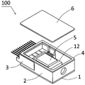
- FIG. 5 is a perspective view showing an embodiment of an electronic apparatus using the electronic component storage package shown in FIG.
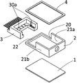
- an electronic component storage package 10 (hereinafter also simply referred to as a package 10) according to an embodiment of the present invention is provided on a substrate 1 and an upper surface of the substrate 1.
- the frame 2 having the hole 20 and the input / output member 3 fixed to the hole 20 are provided.
- an electronic device includes a package 10, an electronic component 5 placed and accommodated in the package 10, and a lid 6 that seals the electronic component 5. And.
- the substrate 1 is a member for hermetically sealing the electronic component 5 together with the frame 2, the input / output member 3 and the lid 6.
- the substrate 1 is a plate-like member having a quadrangular shape when viewed in plan, for example.
- the substrate 1 has a placement area 11 on which the electronic component 5 is placed.
- the mounting substrate 12 is disposed on the upper surface of the substrate 1, and the electronic component 5 is mounted on the upper surface of the mounting substrate 12.
- the placement region 11 means a region where the placement substrate 12 overlaps the substrate 1 when the substrate 1 is viewed in plan.
- the electronic component 5 may be directly mounted on the substrate 1 without using the mounting substrate 12.
- the material of the substrate for example, a metal material such as iron, copper, nickel, chromium, cobalt, or tungsten can be used. Or the alloy or composite material which consists of these metals can be used. By subjecting such an ingot of a metal material to a metal processing method such as a rolling method or a punching method, the substrate 1 can be manufactured.
- a metal processing method such as a rolling method or a punching method
- the mounting substrate 12 for example, a material having good insulation is used.
- a ceramic material such as an aluminum oxide sintered body, a mullite sintered body, a silicon carbide sintered body, an aluminum nitride sintered body, or a silicon nitride sintered body Can be used.
- the frame body 2 is a member for holding the input / output member 3 together with the substrate 1.
- the frame 2 is provided on the upper surface of the substrate 1 so as to surround the placement region 11.
- the frame body 2 is disposed between a pair of first side wall portions 21a and 21b that are disposed to face each other with the placement region 11 therebetween, and between the ends of the pair of first side wall portions 21a and 21b. It has a plurality of side wall portions including the second side wall portion 22 located.
- the frame body 2 has four side wall portions including a pair of first side wall portions 21 (21 a, 21 b) and a second side wall portion 22.
- the frame body 2 further has a third side wall portion 23.
- the third side wall portion 23 is located between the other ends of the pair of first side wall portions 21 and faces the second side wall portion 22.
- the frame 2 has a substantially quadrangular shape on the inner periphery and the outer periphery when viewed in plan.
- the frame body 2 has a hole 20 formed from the second side wall portion 22 to the pair of first side wall portions 21.
- the hole 20 opens on the inner surface and the outer surface of the frame body 2.
- the pair of first side wall portions 21 is formed from the corners of the frame body 2 formed by the first side wall portion 21 a and the second side wall portion 22 of the pair of first side wall portions 21.
- a hole 20 is formed over the corner of the frame 2 formed by the other first side wall 21 b and the second side wall 22.
- the hole 20 is cut from the upper surface of the frame body 2 to the middle of the frame body 2.
- the input / output member 3 is fixed to the hole 20.
- a seal ring 4 surrounding the placement region 11 is attached to the upper part of the frame body 2 and the hole 20 similarly to the frame body 2.
- the seal ring 4 is a member for facilitating the attachment of the lid body 6 but may not be used.
- the seal ring 4 is a separate body from the frame 2, but functionally surrounds the placement region 11 in the same manner as the frame 2 and seals the package. Therefore, the seal ring 4 can be regarded as a part of the frame 2.
- the hole 20 may be cut out from the lower surface of the frame body 2 to the middle of the frame body 2. Moreover, it is good also as the hole 20 which penetrated the frame 2 between the upper surface and the lower surface.
- a metal material such as iron, copper, nickel, chromium, cobalt, or tungsten can be used.
- an alloy made of these metals can be used.
- the frame body 2 and the seal ring 4 can be produced by subjecting such an ingot of a metal material to a metal processing method such as a rolling method or a punching method.
- the frame body 2 has an opening 230 that opens to the inner side surface and the outer side surface in the third side wall portion 23.
- An optical fiber fixing part (not shown) is fixed so as to penetrate through the opening 230.
- the optical fiber fixing part is a cylindrical member.
- the optical fiber fixing portion is provided to fix an optical fiber inserted into the optical fiber fixing portion and to perform optical coupling between the optical fiber and the electronic component 5.
- the package 10 is used for housing an optical semiconductor element.
- the optical fiber fixing portion has at least a strength that can fix the optical fiber.
- a metal material such as iron, copper, nickel, chromium, cobalt, or tungsten can be used.
- an alloy made of these metals can be used.
- a metal processing method such as a rolling method or a punching method to such an ingot of a metal material, an optical fiber fixing portion can be manufactured.
- the frame body 2 and the optical fiber fixing portion are formed of the same metal material. Therefore, the thermal expansion difference between the frame 2 and the optical fiber fixing portion can be reduced. As a result, it is possible to reduce the stress generated between the frame body 2 and the optical fiber holding part under the heat cycle.
- the input / output member 3 is a member for electrically connecting the electronic component 5 and an external circuit.
- the input / output member 3 is fixed to the hole 20 of the frame 2.
- the input / output member 3 has one end located inside the frame 2 and the other end located outside the frame 2.
- the input / output member 3 protrudes in a shelf-like manner on the inside of the first side wall portions 21 a and 21 b and on the inside of the second side wall portion 22 and on the outside of the second side wall portion 22.
- a protruding portion 31b is provided so as to surround a part of the placement region 11 from three directions when the package 10 is viewed in plan.
- the input / output member 3 is formed so as to surround at least a part of the placement region 11 by the inner protruding portion 31a.
- the input / output member 3 is provided with a plate-like first insulating member including the protruding portions 31 (31a, 31b) and a plate-like second insulating member joined to the upper surface of the first insulating member. It is formed by laminating a second insulating member on the first insulating member with a plurality of wiring conductors 32 formed on the upper surface of one insulating member interposed therebetween.
- the first insulating member and the second insulating member used for the input / output member 3 are made of a material having good insulating properties.
- a material constituting these insulating members for example, a ceramic material such as an aluminum oxide sintered body, a mullite sintered body, a silicon carbide sintered body, an aluminum nitride sintered body, or a silicon nitride sintered body is used. Can be used.
- the wiring conductor 32 is provided on the upper surface of the first insulating member.
- the wiring conductor 32 is electrically connected to the electronic component 5 by a bonding wire or via a conductor such as a bonding wire and a wiring pattern provided on the upper surface of the mounting substrate 12.
- the ends of the wiring conductors 32 arranged inside the frame body 2 are arranged so as to surround the mounting region 11 from three directions when the package 10 is viewed in plan.
- the end of the wiring conductor 32 is formed on the surface of the protruding portion 31a. As a result, the distance between the end of the wiring conductor 32 and the mounting substrate 12 or the electronic component 5 can be reduced.
- connection between the wiring conductor 32 and the electronic component 4 by the bonding wire and the conductor such as the wiring pattern provided on the upper surface of the mounting substrate 12 can be performed at a short distance. Further, since these wiring conductors 32 are formed on one input / output member 3, the number of input / output members 3 provided in the package 10 can be reduced. As a result, the frequency characteristics of the package 10 can be improved and the size can be reduced.
- the other end portion of the wiring conductor 32 is drawn to the outside of the second side wall portion 22.
- the other end of the wiring conductor 32 is formed on the surface of the protruding portion 31b.
- the other end of the wiring conductor 32 is formed on the upper surface of the protruding portion 31 b, but it may also be formed on the lower surface of the protruding portion 32 b. Further, more wiring conductors 32 can be provided if they are formed on respective surfaces of stepped shapes with different projecting heights.
- a direct current or an alternating current flows through these wiring conductors 32.
- a DC power supply for the electronic component 5 can be supplied.
- a ground potential can be supplied.
- Many of the wiring conductors 32 are used as low-frequency signal wiring or high-frequency signal wiring.
- the wiring conductor 32 is formed by a metallized layer, for example.
- the metallized layer is formed by coating a predetermined surface of a ceramic green sheet with a conductive paste prepared by mixing an appropriate binder and solvent with metal powders such as W, Mo, and Mn in a predetermined pattern by screen printing, gravure printing, etc. Formed by firing. Thereafter, a metal plating layer made of nickel and gold is formed on the surface of the wiring conductor 32.
- a metallized layer is also formed on the portion of the input / output member 3 joined to the first side wall 21 and the second side wall 22. This metallized layer is formed in order to join to the hole 20 of the frame body 2 through a brazing material.
- a metallized layer is also formed on the upper surface 3a of the input / output member 3, that is, the upper surface 3a of the second insulating member.
- the width of the upper surface 3 a of the second insulating member is larger than the thickness of the first side wall part 21 and the second side wall part 22.
- the seal ring 4 is used, it is larger than the width of the seal ring 4. Therefore, a part of the metallized layer formed on the upper surface of the second insulating member is not covered with the first side wall part 21 and the second side wall part 22 or the seal ring 4, and the first side wall part is formed. 21 and the second side wall 22 are exposed on both sides. Therefore, when this metallized layer and the frame 2 are joined with a brazing material, an excess brazing material for joining the input / output member 3 to the hole 20 is stored in this exposed portion.
- the brazing material collected causes a meniscus between the side surface of the frame body 2 or the side surface of the seal ring 4 and improves the bonding strength between the input / output member 3 and the frame body 2. And the sealing reliability of the electronic device 100 is improved.
- a part of the brazing material becomes a perpendicular joining surface of the vertical end surface of the input / output member 3 and the first side wall portion 21. May flow to the lower surface side of the input / output member 3 through the joint portion, and the brazing material that forms a sufficient meniscus on the upper surface of the input / output member 3 may be insufficient.
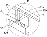
- the input / output member 3 is formed with a constricted portion 30 in which the width of the upper surface 3a is narrowed in a part of the second insulating member.
- the constricted portion 30 is formed on the upper surface 3a joined to the first side wall portion.
- the metallized layer is not formed on the inner side surface of the input / output member 3. Therefore, the flow to the lower surface side of the brazing material that fixes the upper surface 3 a of the input / output member 3 is blocked by the constricted portion 30. And sufficient brazing
- wax material can be collected on the upper surface 3a of the input / output member 3, and joining of the input / output member 3 and the frame 2 or the seal ring 4 can be made sufficient.
- the constricted portion 30 is formed by a concave groove 30 a extending in the vertical direction from the upper end of the wall surface of the input / output member 3.
- the groove 30a By forming the groove 30a on the upper surface 3a, the width of the upper surface 3a becomes narrower at the portion where the groove 30a is formed.
- variety of the metallization layer provided in the upper surface 3a becomes narrow by the ditch
- the constricted portion 30 only needs to be able to narrow the width of the upper surface 3a and the width of the metallized layer, and is not limited to the concave groove 30a, and may be formed by other means.
- the constricted portion 30 may be formed by providing a notch in the side portion of the upper surface 3a.
- the concave groove 30a is formed will be described.
- the metallized layer is not applied to the side wall surface of the second insulating member. Therefore, the surplus brazing material does not wet and spread the side wall surface of the input / output member 3. As a result, surplus brazing material does not adhere to the wiring conductor 32 to cause an electrical connection failure such as a short circuit.
- the width of the upper surface 3a of the input / output member 3 exposed from the outside of the first side wall portion 21 is, for example, 0.17 mm.
- the width of the upper surface 3a of the input / output member 3 exposed from the inside of the first side wall portion 21 is, for example, 0.53 mm.
- the depth of the concave groove 30a is 0.15 mm. Therefore, the distance between the bottom surface of the groove 30a and the first side wall portion 21 is 0.38 mm. That is, the width of the upper surface 3a is 0.53 mm to 0.38 mm at the position of the concave groove 30a.
- the brazing material is difficult to flow through this width.
- the bottom surface of the concave groove 30a is not disposed so as to overlap the lower side of the first side wall portion 21 or the seal ring 4.
- the bottom surface of the concave groove 30a is preferably formed so as to be positioned in the direction inside the package relative to the inner surface of the seal ring 4. It is possible to reduce the possibility that the thermal stress generated in the concave groove 30a due to the difference in thermal expansion with the seal ring 4 deforms the input / output member 3 and is significantly damaged.
- the width of the upper surface 3a may be anything as long as it can block the flow of the brazing material, and an effect is obtained if it is narrowed by 30% to 90% of the width of the upper surface 3a. Preferably, it may be 50% to 80% of the width of the upper surface 3a.
- the concave groove 30 a is preferably provided in a portion close to the terminal end of the input / output member 3.
- the term “end” means a portion farthest from the second side wall portion 22 of the portion joined to the first side wall 21 of the input / output member 3.
- the concave groove 30a is preferably provided on the terminal side from the half position of the portion joined to the first side wall portion 21.
- the concave groove 30a is provided on at least one inner wall surface on the first side wall portion 21a side, but may be provided on the other inner wall surface on the first side wall portion 21b side. As a result, a sufficient amount of brazing material can be accumulated between the formation positions of the two concave grooves 30a on the upper surface 3a. If it is provided only on one side, the brazing material may flow through the other side.
- the concave groove 30a is preferably provided at an approximately equal distance from the second side wall portion 22 on both inner wall surfaces of the first side wall portion 21a and the other first side wall portion 21b.
- the amount of the brazing material flowing on the first side wall portions 21a, 21b side on both sides becomes equal, and the joining force with the first side wall portions 21a, 21b of the input / output member 3 can be made equal.
- brazing material amount is substantially equal, and joining force Should be balanced.
- a concave groove 30 a may be provided on the outer wall surface of the input / output member 3.
- the concave groove 30a is not provided. Because there is little joining margin, the amount of brazing material flowing is not large. Further, since the concave groove 30a is provided on the inner side surface but not on the outer side surface, the package 10 is reduced in size accordingly.
- the concave groove 30a is provided in a curved shape between the bottom surface and the inner surface. Thereby, it is suppressed that the thermal stress which arises by the thermal expansion difference with the frame 2, the input / output terminal 3, and the seal ring 4 concentrates on a part between the bottom face and inner surface of the ditch
- FIG. 2 shows an example in which the wiring conductors 32a and 32b and the wiring conductors 32c and 32d are arranged in two rows from the bottom surface of the concave groove 30a toward the end surface of the protruding portion 31a.
- the input / output member 3 further includes a side metallization layer around the outer wall surface of the input / output member 3 that is in contact with the first sidewall portion 21, the second sidewall portion 22, and the joint surface joined to the seal ring 4. May be.
- the side metallization layer is provided to wet and spread the brazing material that joins the input / output member 3 and the frame 2 to a part of the outer wall surface of the input / output member 3.
- the brazing material is provided across the side wall surface of the input / output member 3 from the joint interface between the frame 2 and the input / output member 3.
- the joint strength between the input / output member 3 and the frame body 2 can be improved, and the sealing performance can be improved.
- the electronic device 100 includes the package 10, the electronic component 5, and the lid 6.
- the electronic component 5 is placed on the placement area 11 of the substrate 1.
- the electronic component 5 is electrically connected to the wiring conductor 32 of the input / output member 3 via a wiring pattern and a bonding wire provided on the upper surface of the mounting substrate 12.
- Examples of the electronic component 5 include an electronic component such as an optical semiconductor element, an IC element, or a capacitor.
- an optical semiconductor element is used as the electronic component 5.
- an optical semiconductor element for example, a light emitting element that emits light to an optical fiber typified by an LD (laser diode) element, or light from an optical fiber typified by a PD (photodiode) element is received.
- LD laser diode
- PD photodiode
- the lid 6 is a member for hermetically sealing the electronic component 5 together with the substrate 1, the input / output member 3 and the frame 2.
- the lid body 6 is joined to the upper surface of the frame body 2 or the upper surface of the seal ring 4.
- the electronic component 5 is hermetically sealed in a space surrounded by the substrate 1, the frame 2, the input / output member 3, and the lid 6.
- a metal member such as iron, copper, nickel, chromium, cobalt, or tungsten, or an alloy or composite member made of these metals can be used.
- the frame body 2 and the lid body 6 are joined together by, for example, a brazing material.
- the substrate 1 has a quadrangular shape, but is not limited thereto. Specifically, it may be circular or polygonal.
- the placement area 11 is formed at the center of the upper surface of the substrate 1, but is not limited thereto. Specifically, the placement region 11 may be provided at the end of the upper surface of the substrate 1. In this case, the frame body 2 may also be provided at the end of the upper surface of the substrate 1 so as to surround the placement region 11.
- the substrate 1 has only one placement region 11, but the present invention is not limited to this. Specifically, the substrate 1 may have a plurality of placement areas 11, and separate electronic components 5 may be placed in each placement area 11.
- the frame body 2 has four side wall portions, but is not limited thereto.
- the frame 2 may have five or more side walls, and may have a polygonal shape in plan view.
- the frame body 2 is integrally formed, but is not limited thereto.
- the pair of first sidewall portions 21 and second sidewall portions 22 may be formed separately.
- the pair of first side wall portion 21 and second side wall portion 22 may be joined by a joining member such as a brazing material.
- Substrate 11 Placement region 12: Placement substrate 2: Frame body 20: Hole 21: First sidewall 22: Second sidewall 23: Third sidewall 230: Opening 3: Input / output Member 3a: Upper surface 30: Constricted portion 30a: Groove 31a, 31b: Protruding portion 32: Wiring conductor 4: Seal ring 5: Electronic component 6: Lid 10: Electronic component storage package (package) 100: Electronic device
Landscapes
- Physics & Mathematics (AREA)
- Engineering & Computer Science (AREA)
- Power Engineering (AREA)
- Condensed Matter Physics & Semiconductors (AREA)
- General Physics & Mathematics (AREA)
- Electromagnetism (AREA)
- Optics & Photonics (AREA)
- Manufacturing & Machinery (AREA)
- Microelectronics & Electronic Packaging (AREA)
- Piezo-Electric Or Mechanical Vibrators, Or Delay Or Filter Circuits (AREA)
- Semiconductor Lasers (AREA)
Abstract
Description
11:載置領域
12:載置基板
2:枠体
20:孔部
21:第1の側壁部
22:第2の側壁部
23:第3の側壁部
230:開口部
3:入出力部材
3a:上面
30:くびれ部
30a:凹溝
31a,31b:突出部
32:配線導体
4:シールリング
5:電子部品
6:蓋体
10:電子部品収納用パッケージ(パッケージ)
100:電子装置
Claims (6)
- 電子部品が載置される載置領域を上面に有する金属製の基板と、
前記載置領域を間に挟むように対置された一対の第1の側壁部および該一対の第1の側壁部の端部同士を接続するように配置された第2の側壁部を含む複数の側壁部からなるとともに、前記第2の側壁部から前記一対の第1の側壁部にかけて内側面および外側面に開口する孔部を有し、前記載置領域を囲むように前記基板の上面に設けられた金属製の枠体と、
前記孔部にろう材を介して接合されるとともに、前記一対の第1の側壁部および前記第2の側壁部の内側並びに前記第2の側壁部の外側に突出部を有し、該突出部に前記電子部品に電気的に接続される複数の配線導体を有する入出力部材とを備えた電子部品収納用パッケージであって、
前記入出力部材は、前記第1の側壁部および前記第2の側壁部に接合される上面を有し、該上面は、前記第1の側壁部と接合される部分に幅が狭いくびれ部を備えていることを特徴とする電子部品収納用パッケージ。 - 前記入出力端子の壁面上端に上下方向に伸びる凹溝が形成されていることによって、前記くびれ部が形成されていることを特徴とする請求項1記載の電子部品収納用パッケージ。
- 前記凹溝は、前記入出力端子の内壁面に設けられていることを特徴とする請求項2記載の電子部品収納用パッケージ。
- 前記凹溝は、前記一対の第1の側壁部に接合される壁面にそれぞれ設けられていることを特徴とする請求項2または3記載の電子部品収納用パッケージ。
- 前記凹溝は、前記第2の側壁部から等距離の前記第1の側壁部に接合される壁面にそれぞれ設けられていることを特徴とする請求項4記載の電子部品収納用パッケージ。
- 請求項1乃至請求項5のいずれか1つに記載の電子部品収納用パッケージと、
該電子部品収納用パッケージの前記載置領域に載置されて、導体を介して前記配線導体に接続された電子部品と、
前記枠体の上面に接合された、前記電子部品を封止する蓋体とを備えた電子装置。
Priority Applications (3)
| Application Number | Priority Date | Filing Date | Title |
|---|---|---|---|
| CN201480023631.3A CN105144370B (zh) | 2013-09-25 | 2014-09-25 | 电子部件收纳用封装件以及电子装置 |
| JP2015539290A JP5981660B2 (ja) | 2013-09-25 | 2014-09-25 | 電子部品収納用パッケージおよび電子装置 |
| US14/787,496 US9640452B2 (en) | 2013-09-25 | 2014-09-25 | Electronic component housing package and electronic device |
Applications Claiming Priority (2)
| Application Number | Priority Date | Filing Date | Title |
|---|---|---|---|
| JP2013198454 | 2013-09-25 | ||
| JP2013-198454 | 2013-09-25 |
Publications (1)
| Publication Number | Publication Date |
|---|---|
| WO2015046292A1 true WO2015046292A1 (ja) | 2015-04-02 |
Family
ID=52743426
Family Applications (1)
| Application Number | Title | Priority Date | Filing Date |
|---|---|---|---|
| PCT/JP2014/075362 Ceased WO2015046292A1 (ja) | 2013-09-25 | 2014-09-25 | 電子部品収納用パッケージおよび電子装置 |
Country Status (4)
| Country | Link |
|---|---|
| US (1) | US9640452B2 (ja) |
| JP (1) | JP5981660B2 (ja) |
| CN (1) | CN105144370B (ja) |
| WO (1) | WO2015046292A1 (ja) |
Cited By (3)
| Publication number | Priority date | Publication date | Assignee | Title |
|---|---|---|---|---|
| EP3300104A4 (en) * | 2015-05-20 | 2019-01-09 | Kyocera Corporation | SEMICONDUCTOR ELEMENT HOUSING, SEMICONDUCTOR ELEMENT AND MOUNTING STRUCTURE |
| JP2021064812A (ja) * | 2017-02-23 | 2021-04-22 | 京セラ株式会社 | 絶縁基体、半導体パッケージおよび半導体装置 |
| JP2021090078A (ja) * | 2015-12-25 | 2021-06-10 | 京セラ株式会社 | 光半導体素子収納用パッケージおよび光半導体装置 |
Families Citing this family (10)
| Publication number | Priority date | Publication date | Assignee | Title |
|---|---|---|---|---|
| CN106415821B (zh) * | 2014-01-24 | 2019-03-01 | 京瓷株式会社 | 元件收纳用封装以及安装结构体 |
| CN106062946B (zh) * | 2014-03-13 | 2018-10-23 | 京瓷株式会社 | 电子部件收纳用封装件以及电子装置 |
| EP3170228B1 (en) * | 2014-07-16 | 2019-05-01 | Siemens Aktiengesellschaft | Subsea electrical connector component and method of manufacturing thereof |
| US10014189B2 (en) * | 2015-06-02 | 2018-07-03 | Ngk Spark Plug Co., Ltd. | Ceramic package with brazing material near seal member |
| CN109075526B (zh) * | 2016-04-18 | 2022-05-31 | 京瓷株式会社 | 发光元件收纳用构件及发光装置 |
| WO2018109820A1 (ja) * | 2016-12-13 | 2018-06-21 | 新電元工業株式会社 | 電子モジュール |
| CN108767652B (zh) * | 2018-05-31 | 2020-06-16 | 北京航空航天大学 | 一种半导体激光器一体化结构 |
| EP3876272A4 (en) * | 2018-10-30 | 2022-08-17 | Kyocera Corporation | HOUSING FOR HOUSING AN ELECTRONIC COMPONENT AND ELECTRONIC DEVICE |
| EP4191657B1 (en) * | 2020-08-03 | 2025-10-01 | NTT, Inc. | Package and production method therefor |
| JP7443281B2 (ja) * | 2021-03-22 | 2024-03-05 | 株式会社東芝 | 配線装置 |
Citations (3)
| Publication number | Priority date | Publication date | Assignee | Title |
|---|---|---|---|---|
| JP2004235363A (ja) * | 2003-01-29 | 2004-08-19 | Kyocera Corp | 半導体素子収納用パッケージおよび半導体装置 |
| JP2006066867A (ja) * | 2004-02-26 | 2006-03-09 | Kyocera Corp | 電子部品収納用パッケージおよび電子装置 |
| JP2006179839A (ja) * | 2004-11-29 | 2006-07-06 | Kyocera Corp | 接続端子ならびにこれを用いた電子部品収納用パッケージおよび電子装置 |
Family Cites Families (15)
| Publication number | Priority date | Publication date | Assignee | Title |
|---|---|---|---|---|
| US5018050A (en) * | 1987-11-17 | 1991-05-21 | Omron Tateisi Electronics Co. | Solid state relay |
| DE68921115T2 (de) * | 1988-07-25 | 1995-10-12 | Asahi Glass Co Ltd | Fensterscheibenantenne für ein Kraftfahrzeug. |
| JP2854460B2 (ja) | 1992-05-28 | 1999-02-03 | 京セラ株式会社 | 半導体素子収納用パッケージ |
| JP3500268B2 (ja) * | 1997-02-27 | 2004-02-23 | 京セラ株式会社 | 高周波用入出力端子ならびにそれを用いた高周波用半導体素子収納用パッケージ |
| JPH1117041A (ja) * | 1997-06-20 | 1999-01-22 | Sumitomo Electric Ind Ltd | 光半導体用パッケージ |
| JP4070181B2 (ja) | 2001-06-27 | 2008-04-02 | 京セラ株式会社 | 半導体素子収納用パッケージおよび半導体装置 |
| US6992250B2 (en) * | 2004-02-26 | 2006-01-31 | Kyocera Corporation | Electronic component housing package and electronic apparatus |
| JP5189597B2 (ja) * | 2007-10-30 | 2013-04-24 | 京セラ株式会社 | 接続端子及びこれを用いたパッケージ並びに電子装置 |
| JP2009122451A (ja) * | 2007-11-15 | 2009-06-04 | Hitachi Chem Co Ltd | 光学接続構造 |
| WO2012015040A1 (ja) * | 2010-07-30 | 2012-02-02 | 京セラ株式会社 | 電子部品収納用部品、電子モジュールおよび電子装置 |
| US9237662B2 (en) * | 2010-09-28 | 2016-01-12 | Kyocera Corporation | Device housing package and electronic apparatus employing the same |
| WO2013077199A1 (ja) * | 2011-11-21 | 2013-05-30 | 京セラ株式会社 | 電子部品収納用パッケージおよび電子装置 |
| WO2014002921A1 (ja) * | 2012-06-26 | 2014-01-03 | 京セラ株式会社 | 半導体素子収納用パッケージおよび半導体装置 |
| JP5898332B2 (ja) * | 2012-10-30 | 2016-04-06 | 京セラ株式会社 | 電子部品収納用容器および電子装置 |
| US9287882B2 (en) * | 2013-11-07 | 2016-03-15 | Kyocera Crystal Device Corporation | Temperature compensated crystal oscillator |
-
2014
- 2014-09-25 JP JP2015539290A patent/JP5981660B2/ja not_active Expired - Fee Related
- 2014-09-25 CN CN201480023631.3A patent/CN105144370B/zh active Active
- 2014-09-25 WO PCT/JP2014/075362 patent/WO2015046292A1/ja not_active Ceased
- 2014-09-25 US US14/787,496 patent/US9640452B2/en active Active
Patent Citations (3)
| Publication number | Priority date | Publication date | Assignee | Title |
|---|---|---|---|---|
| JP2004235363A (ja) * | 2003-01-29 | 2004-08-19 | Kyocera Corp | 半導体素子収納用パッケージおよび半導体装置 |
| JP2006066867A (ja) * | 2004-02-26 | 2006-03-09 | Kyocera Corp | 電子部品収納用パッケージおよび電子装置 |
| JP2006179839A (ja) * | 2004-11-29 | 2006-07-06 | Kyocera Corp | 接続端子ならびにこれを用いた電子部品収納用パッケージおよび電子装置 |
Cited By (7)
| Publication number | Priority date | Publication date | Assignee | Title |
|---|---|---|---|---|
| EP3300104A4 (en) * | 2015-05-20 | 2019-01-09 | Kyocera Corporation | SEMICONDUCTOR ELEMENT HOUSING, SEMICONDUCTOR ELEMENT AND MOUNTING STRUCTURE |
| JP2021090078A (ja) * | 2015-12-25 | 2021-06-10 | 京セラ株式会社 | 光半導体素子収納用パッケージおよび光半導体装置 |
| JP7193565B2 (ja) | 2015-12-25 | 2022-12-20 | 京セラ株式会社 | 光半導体素子収納用パッケージおよび光半導体装置 |
| JP2021064812A (ja) * | 2017-02-23 | 2021-04-22 | 京セラ株式会社 | 絶縁基体、半導体パッケージおよび半導体装置 |
| JP7007502B2 (ja) | 2017-02-23 | 2022-01-24 | 京セラ株式会社 | 絶縁基体、半導体パッケージおよび半導体装置 |
| JP2022046748A (ja) * | 2017-02-23 | 2022-03-23 | 京セラ株式会社 | 絶縁基体、半導体パッケージおよび半導体装置 |
| JP7350902B2 (ja) | 2017-02-23 | 2023-09-26 | 京セラ株式会社 | 絶縁基体、半導体パッケージおよび半導体装置 |
Also Published As
| Publication number | Publication date |
|---|---|
| JPWO2015046292A1 (ja) | 2017-03-09 |
| US9640452B2 (en) | 2017-05-02 |
| US20160104650A1 (en) | 2016-04-14 |
| CN105144370A (zh) | 2015-12-09 |
| CN105144370B (zh) | 2017-11-14 |
| JP5981660B2 (ja) | 2016-08-31 |
Similar Documents
| Publication | Publication Date | Title |
|---|---|---|
| JP5981660B2 (ja) | 電子部品収納用パッケージおよび電子装置 | |
| CN104396006B (zh) | 半导体元件收纳用封装件以及半导体装置 | |
| JP5518260B2 (ja) | 素子収納用パッケージ、半導体装置用部品および半導体装置 | |
| JP5537736B2 (ja) | 半導体素子収納用パッケージ、これを備えた半導体装置および電子装置 | |
| CN104428888B (zh) | 电子部件收纳用容器以及电子装置 | |
| JP6243510B2 (ja) | 電子部品収納用パッケージおよび電子装置 | |
| JP6314591B2 (ja) | 半導体装置および半導体装置の製造方法 | |
| US20200273825A1 (en) | Semiconductor device | |
| JP2013074048A (ja) | 半導体素子収納用パッケージおよび半導体装置 | |
| JP6166101B2 (ja) | 光半導体素子収納用パッケージおよびこれを備えた実装構造体 | |
| JP5812671B2 (ja) | 素子収納用パッケージおよびこれを備えた半導体装置 | |
| WO2013042627A1 (ja) | 電子部品載置用基板、電子部品収納用パッケージおよび電子装置 | |
| JP5709427B2 (ja) | 素子収納用パッケージおよびこれを備えた半導体装置 | |
| JP6034054B2 (ja) | 電子部品収納用パッケージおよび電子装置 | |
| CN105164801B (zh) | 元件收纳用封装件以及具备其的安装结构体 | |
| JP2004356391A (ja) | 半導体素子収納用パッケージおよび半導体装置 | |
| JP2012248777A (ja) | 素子収納用パッケージおよびこれを備えた半導体モジュール | |
| JP2014007368A (ja) | 電子部品収納用パッケージおよび電子装置 | |
| JP6022842B2 (ja) | 半導体素子収納用パッケージおよび半導体装置 | |
| KR20150139190A (ko) | 소자 및 소자 패키지 | |
| JP2013012592A (ja) | 素子収納用パッケージおよびこれを備えたモジュール | |
| JP2019041072A (ja) | 電子部品収納用パッケージおよび電子装置 | |
| JP2012234880A (ja) | 素子収納用パッケージおよびこれを備えた半導体装置 |
Legal Events
| Date | Code | Title | Description |
|---|---|---|---|
| WWE | Wipo information: entry into national phase |
Ref document number: 201480023631.3 Country of ref document: CN |
|
| 121 | Ep: the epo has been informed by wipo that ep was designated in this application |
Ref document number: 14850084 Country of ref document: EP Kind code of ref document: A1 |
|
| ENP | Entry into the national phase |
Ref document number: 2015539290 Country of ref document: JP Kind code of ref document: A |
|
| WWE | Wipo information: entry into national phase |
Ref document number: 14787496 Country of ref document: US |
|
| NENP | Non-entry into the national phase |
Ref country code: DE |
|
| 122 | Ep: pct application non-entry in european phase |
Ref document number: 14850084 Country of ref document: EP Kind code of ref document: A1 |