WO2015045476A1 - 電子顕微鏡 - Google Patents
電子顕微鏡 Download PDFInfo
- Publication number
- WO2015045476A1 WO2015045476A1 PCT/JP2014/063016 JP2014063016W WO2015045476A1 WO 2015045476 A1 WO2015045476 A1 WO 2015045476A1 JP 2014063016 W JP2014063016 W JP 2014063016W WO 2015045476 A1 WO2015045476 A1 WO 2015045476A1
- Authority
- WO
- WIPO (PCT)
- Prior art keywords
- sample
- electron beam
- image
- electron
- imaging lens
- Prior art date
- Legal status (The legal status is an assumption and is not a legal conclusion. Google has not performed a legal analysis and makes no representation as to the accuracy of the status listed.)
- Ceased
Links
Images







Classifications
-
- H—ELECTRICITY
- H01—ELECTRIC ELEMENTS
- H01J—ELECTRIC DISCHARGE TUBES OR DISCHARGE LAMPS
- H01J37/00—Discharge tubes with provision for introducing objects or material to be exposed to the discharge, e.g. for the purpose of examination or processing thereof
- H01J37/02—Details
- H01J37/04—Arrangements of electrodes and associated parts for generating or controlling the discharge, e.g. electron-optical arrangement or ion-optical arrangement
- H01J37/10—Lenses
-
- G—PHYSICS
- G01—MEASURING; TESTING
- G01N—INVESTIGATING OR ANALYSING MATERIALS BY DETERMINING THEIR CHEMICAL OR PHYSICAL PROPERTIES
- G01N23/00—Investigating or analysing materials by the use of wave or particle radiation, e.g. X-rays or neutrons, not covered by groups G01N3/00 – G01N17/00, G01N21/00 or G01N22/00
- G01N23/20—Investigating or analysing materials by the use of wave or particle radiation, e.g. X-rays or neutrons, not covered by groups G01N3/00 – G01N17/00, G01N21/00 or G01N22/00 by using diffraction of the radiation by the materials, e.g. for investigating crystal structure; by using scattering of the radiation by the materials, e.g. for investigating non-crystalline materials; by using reflection of the radiation by the materials
- G01N23/20058—Measuring diffraction of electrons, e.g. low energy electron diffraction [LEED] method or reflection high energy electron diffraction [RHEED] method
-
- H—ELECTRICITY
- H01—ELECTRIC ELEMENTS
- H01J—ELECTRIC DISCHARGE TUBES OR DISCHARGE LAMPS
- H01J37/00—Discharge tubes with provision for introducing objects or material to be exposed to the discharge, e.g. for the purpose of examination or processing thereof
- H01J37/02—Details
- H01J37/04—Arrangements of electrodes and associated parts for generating or controlling the discharge, e.g. electron-optical arrangement or ion-optical arrangement
-
- H—ELECTRICITY
- H01—ELECTRIC ELEMENTS
- H01J—ELECTRIC DISCHARGE TUBES OR DISCHARGE LAMPS
- H01J37/00—Discharge tubes with provision for introducing objects or material to be exposed to the discharge, e.g. for the purpose of examination or processing thereof
- H01J37/02—Details
- H01J37/04—Arrangements of electrodes and associated parts for generating or controlling the discharge, e.g. electron-optical arrangement or ion-optical arrangement
- H01J37/05—Electron or ion-optical arrangements for separating electrons or ions according to their energy or mass
-
- H—ELECTRICITY
- H01—ELECTRIC ELEMENTS
- H01J—ELECTRIC DISCHARGE TUBES OR DISCHARGE LAMPS
- H01J37/00—Discharge tubes with provision for introducing objects or material to be exposed to the discharge, e.g. for the purpose of examination or processing thereof
- H01J37/02—Details
- H01J37/04—Arrangements of electrodes and associated parts for generating or controlling the discharge, e.g. electron-optical arrangement or ion-optical arrangement
- H01J37/09—Diaphragms; Shields associated with electron or ion-optical arrangements; Compensation of disturbing fields
-
- H—ELECTRICITY
- H01—ELECTRIC ELEMENTS
- H01J—ELECTRIC DISCHARGE TUBES OR DISCHARGE LAMPS
- H01J37/00—Discharge tubes with provision for introducing objects or material to be exposed to the discharge, e.g. for the purpose of examination or processing thereof
- H01J37/02—Details
- H01J37/04—Arrangements of electrodes and associated parts for generating or controlling the discharge, e.g. electron-optical arrangement or ion-optical arrangement
- H01J37/147—Arrangements for directing or deflecting the discharge along a desired path
-
- H—ELECTRICITY
- H01—ELECTRIC ELEMENTS
- H01J—ELECTRIC DISCHARGE TUBES OR DISCHARGE LAMPS
- H01J37/00—Discharge tubes with provision for introducing objects or material to be exposed to the discharge, e.g. for the purpose of examination or processing thereof
- H01J37/02—Details
- H01J37/04—Arrangements of electrodes and associated parts for generating or controlling the discharge, e.g. electron-optical arrangement or ion-optical arrangement
- H01J37/147—Arrangements for directing or deflecting the discharge along a desired path
- H01J37/1472—Deflecting along given lines
-
- H—ELECTRICITY
- H01—ELECTRIC ELEMENTS
- H01J—ELECTRIC DISCHARGE TUBES OR DISCHARGE LAMPS
- H01J37/00—Discharge tubes with provision for introducing objects or material to be exposed to the discharge, e.g. for the purpose of examination or processing thereof
- H01J37/02—Details
- H01J37/04—Arrangements of electrodes and associated parts for generating or controlling the discharge, e.g. electron-optical arrangement or ion-optical arrangement
- H01J37/153—Electron-optical or ion-optical arrangements for the correction of image defects, e.g. stigmators
-
- H—ELECTRICITY
- H01—ELECTRIC ELEMENTS
- H01J—ELECTRIC DISCHARGE TUBES OR DISCHARGE LAMPS
- H01J37/00—Discharge tubes with provision for introducing objects or material to be exposed to the discharge, e.g. for the purpose of examination or processing thereof
- H01J37/02—Details
- H01J37/24—Circuit arrangements not adapted to a particular application of the tube and not otherwise provided for
-
- H—ELECTRICITY
- H01—ELECTRIC ELEMENTS
- H01J—ELECTRIC DISCHARGE TUBES OR DISCHARGE LAMPS
- H01J37/00—Discharge tubes with provision for introducing objects or material to be exposed to the discharge, e.g. for the purpose of examination or processing thereof
- H01J37/02—Details
- H01J37/244—Detectors; Associated components or circuits therefor
-
- H—ELECTRICITY
- H01—ELECTRIC ELEMENTS
- H01J—ELECTRIC DISCHARGE TUBES OR DISCHARGE LAMPS
- H01J37/00—Discharge tubes with provision for introducing objects or material to be exposed to the discharge, e.g. for the purpose of examination or processing thereof
- H01J37/26—Electron or ion microscopes; Electron or ion diffraction tubes
-
- H—ELECTRICITY
- H01—ELECTRIC ELEMENTS
- H01J—ELECTRIC DISCHARGE TUBES OR DISCHARGE LAMPS
- H01J37/00—Discharge tubes with provision for introducing objects or material to be exposed to the discharge, e.g. for the purpose of examination or processing thereof
- H01J37/26—Electron or ion microscopes; Electron or ion diffraction tubes
- H01J37/261—Details
-
- H—ELECTRICITY
- H01—ELECTRIC ELEMENTS
- H01J—ELECTRIC DISCHARGE TUBES OR DISCHARGE LAMPS
- H01J37/00—Discharge tubes with provision for introducing objects or material to be exposed to the discharge, e.g. for the purpose of examination or processing thereof
- H01J37/26—Electron or ion microscopes; Electron or ion diffraction tubes
- H01J37/28—Electron or ion microscopes; Electron or ion diffraction tubes with scanning beams
-
- H—ELECTRICITY
- H01—ELECTRIC ELEMENTS
- H01J—ELECTRIC DISCHARGE TUBES OR DISCHARGE LAMPS
- H01J37/00—Discharge tubes with provision for introducing objects or material to be exposed to the discharge, e.g. for the purpose of examination or processing thereof
- H01J37/26—Electron or ion microscopes; Electron or ion diffraction tubes
- H01J37/285—Emission microscopes, e.g. field-emission microscopes
-
- H—ELECTRICITY
- H01—ELECTRIC ELEMENTS
- H01J—ELECTRIC DISCHARGE TUBES OR DISCHARGE LAMPS
- H01J37/00—Discharge tubes with provision for introducing objects or material to be exposed to the discharge, e.g. for the purpose of examination or processing thereof
- H01J37/26—Electron or ion microscopes; Electron or ion diffraction tubes
- H01J37/295—Electron or ion diffraction tubes
-
- G—PHYSICS
- G01—MEASURING; TESTING
- G01N—INVESTIGATING OR ANALYSING MATERIALS BY DETERMINING THEIR CHEMICAL OR PHYSICAL PROPERTIES
- G01N2223/00—Investigating materials by wave or particle radiation
- G01N2223/40—Imaging
- G01N2223/418—Imaging electron microscope
-
- H—ELECTRICITY
- H01—ELECTRIC ELEMENTS
- H01J—ELECTRIC DISCHARGE TUBES OR DISCHARGE LAMPS
- H01J2237/00—Discharge tubes exposing object to beam, e.g. for analysis treatment, etching, imaging
- H01J2237/21—Focus adjustment
-
- H—ELECTRICITY
- H01—ELECTRIC ELEMENTS
- H01J—ELECTRIC DISCHARGE TUBES OR DISCHARGE LAMPS
- H01J2237/00—Discharge tubes exposing object to beam, e.g. for analysis treatment, etching, imaging
- H01J2237/26—Electron or ion microscopes
- H01J2237/2614—Holography or phase contrast, phase related imaging in general, e.g. phase plates
Definitions
- the present invention relates to an electron microscope and a sample observation method using an electron microscope.
- Lorentz microscopy was developed as a technique for observing how an electron beam transmitted through a magnetic material is deflected by the Lorentz force due to the magnetization of the sample.
- Today however, it is accepted as a visualization method for electron beams deflected by interactions different from Bragg diffraction due to crystal structures, such as dielectric polarization and strain fields, as well as magnetic materials, as a visualization method for the deflection state of electron beams.
- the Lorentz method can be broadly divided into two methods: Foucault method and Fresnel method (Non-Patent Document 1).
- the Fresnel method is a method for observing a domain wall
- the Foucault method is a method for observing a magnetic domain. is there.
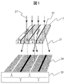
- FIG. 1 shows a state where an electron beam is deflected in a magnetic sample having a 180-degree reversal magnetic domain structure.
- the angle at which the electron beam is deflected depends on the magnitude of magnetization and the thickness of the sample. Therefore, in the case of a sample having a constant thickness and uniform magnetization, the deflection received by the electron beam is the same in any region, and the azimuth and direction differ with the magnetic domain structure.
- the electron beam 27 when the electron beam 27 is incident on the sample 3 having a 180-degree reversal magnetic domain structure, the electron beam 27 transmitted through the sample 3 is deflected in the opposite direction by the respective magnetic domains (31, 33).
- the Fresnel method forms an image of the intensity of the electron beam on the projection surface 24.
- the graph 25 of the intensity distribution of the electron beam on the projection plane is illustrated in the lower part of FIG.
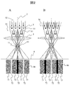
- FIG. 2 is a schematic diagram of an optical system when a magnetic sample is observed by the Fresnel method.
- a Fresnel image 86 is illustrated.
- FIG. 2A shows a state of focusing on the space position 35 on the lower side of the sample, not the sample.
- the domain wall 32 is observed with a contrast 72 of a bright line (white) or a dark line (black).
- FIG. 2B the domain wall 32 is observed with a reverse contrast 72 even when the space position 36 on the upper side of the sample is focused. That is, by observing the sample out of focus, the boundary line of the region that deflects the electron beam is observed as a bright line (white) or a dark line (black).
- the black and white contrast of the border line of the Fresnel image at this time depends on the combination of the deflection directions and the focus position. Also, the amount of defocusing (defocusing amount) depends on the amount of deflection that the electron beam receives, and when it is greatly deflected, sufficient contrast can be obtained with a small defocusing amount of about several hundred nm, For example, in the case of an observation target that gives only a small deflection such as magnetic flux quantum, a defocus amount of several hundred mm is required.
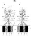
- FIG. 3 shows an optical system for observing the magnetic domain structure by the Foucault method.
- the electron beams transmitted through the sample 3 having the 180 ° reversal magnetic domain structure are deflected in opposite directions by the respective magnetic domains (31, 33).
- spots (11, 13) are formed at positions according to the deflection angle. Therefore, the objective aperture 55 is inserted, and only the electron beam that has passed through the magnetic domain to be observed is selected and imaged on the image plane 7.
- FIG. 1 shows an optical system for observing the magnetic domain structure by the Foucault method.
- FIG. 3A shows an example in which an electron beam that has passed through the magnetic domain 31 and is deflected in the left direction on the paper surface is selected.
- FIG. 3B conversely selects an electron beam that has passed through the magnetic domain 33 and is deflected in the right direction on the paper surface.
- the selected magnetic domains are observed as white, and the unselected magnetic domains are observed as black (no electron beam comes).
- each magnetic domain (31, 33) is striped ( 71, 73) as a Foucault image 84.
- the deflection angle of the electron beam is as small as about 1/10 of the Bragg angle due to crystalline samples.
- An objective aperture with a small hole diameter must be used, and the spatial resolution obtained is about 1/10 times the lattice resolution, which is not significantly different from the Fresnel method.
- the cause of the contrast for observing the magnetic domain structure is due to shielding of the electron beam that has passed through the magnetic domain that is not observed, and this is a technique for obtaining the contrast by discarding some information.
- the objective aperture is adjusted again, and an inverse contrast Foucault image is separately observed, or the objective aperture is removed from the optical axis. Therefore, it was necessary to observe a normal electron microscope image together. That is, multiple observations are necessary, and dynamic observation and real-time observation are almost impossible.
- “lens-less” means that the objective lens is turned off and is not used for image formation. Details of this method will be described later.
- the present invention was made in order to reduce the burden on the operation of the electron microscope operator in performing the lensless Foucault method and to carry out an effective experiment. (This is related to the control of the optical system by the Foucault method.)
- Non-Patent Document 4 electron beam holography
- intensity transport equation method Non-Patent Document 5
- Each method has its advantages, but it requires a highly coherent electron beam such as a field emission electron beam.
- electron holography requires an electron biprism as an additional device.
- the intensity transport equation method requires at least two images with known defocus amounts (conveniently three images) across the in-focus, In reality, adjustment processing such as magnification and alignment of each image is indispensable.
- Non-Patent Document 6 a method of observing a deflection angle of an electron beam due to magnetization in a sample as a diffraction spot on a diffraction surface has been implemented.
- This technique was used in the 1960s to observe a small deflection angle of an electron beam as a diffraction pattern on the diffraction surface (that is, as a diffraction pattern of a large camera length).
- Technology This is an effective method for obtaining information on the average deflection angle.
- the deflection angle of an electron beam becomes small due to the miniaturization and thinning of magnetic elements, the minute deflection angle of transmitted electrons by individual elements is detected. Instead, it is reviewed as a method of detecting the deflection angle of the transmission electron beam received from the entire irradiation region of the electron beam on the diffraction surface.
- Table 1 summarizes the main observation target, the deflection angle received by an electron beam with an acceleration voltage of 300 kV, and the camera length required for observation.
- the Foucault method and the small-angle diffraction method In order to perform the Foucault method optimally, it is necessary to appropriately use an angle limiting diaphragm on the diffraction surface.
- an angle limiting diaphragm For example, in the case of a magnetic material with a thickness of 50 nm (magnetization 1T (Tesla)) that can be easily transmitted with an electron beam with an acceleration voltage of 300 kV, the magnetic deflection angle is approximately 2 ⁇ 10 -5 rad. The angle is almost three orders of magnitude smaller than the diffraction angle. Therefore, in the Foucault method, in order to increase the imaging accuracy, a small angle diffraction method must be realized.
- the Lorentz method has been described as a magnetic material observation method using a transmission electron microscope.
- the observation target is not limited to a magnetic material.
- it has the same technical aspect as phase contrast electron microscopy for biological samples, organic samples, and the like.
- the Lorentz method especially the lensless Foucault method, which realizes the Foucault method, applies an angle-limited aperture to the sample transmission electron beam with the objective lens off.
- the irradiation optical system should not be changed after the observation conditions are determined, and the switching between the sample image observation mode and the sample diffraction pattern observation mode can be realized with good reproducibility.
- there are more restrictions than in the conventional observation method such as not changing the irradiation optical system at the time of switching, and there is a tendency that the burden on the operation of the operator of the electron microscope increases.
- the optical system in order to obtain information about diffraction spots that do not contribute to imaging, the optical system is set to the diffraction pattern observation mode as a procedure, and then the diffraction pattern is confirmed, and the angle limiting diaphragm is properly inserted.
- Switch to the image observation mode, observe and record the Foucault sample image set the optical system to the diffraction pattern observation mode again, properly incorporate the diffraction spot different from the previous observation into the angle limiting diaphragm, and observe the optical system again
- the Foucault image must be observed and recorded as a mode, and the optical system must be set to a diffraction pattern observation mode. In such an experimental situation, the burden reduction during the operation of the electron microscope was an important factor in conducting a high-quality experiment.
- the present invention relates to a control method, control conditions, etc. that are implemented in order to reduce the burden on the operation of the electron microscope operator when performing the lensless Foucault method.
- the lensless Foucault method After confirming the observation conditions, the irradiation optical system must not be changed, but by introducing a condition fixing operation for the irradiation lens, it is possible to prevent erroneous operation after the determination of the use conditions of the irradiation optical system and
- a control method is implemented such that the excitation condition of the imaging lens is memorized to match the lens condition immediately after the switching with the last observation condition in the previous mode. This provides an electron microscope or an observation method that can implement the lensless Foucault method without burdening the operator of the electron microscope.
- the trouble of optical readjustment due to erroneous operation The burden on the operation of the operator of the electron microscope can be reduced to the same extent as the operation of the conventional electron microscope. That is, the lensless Foucault method can be easily implemented.
- the simplicity of implementation has the effect of shortening the time required for readjustment of the optical system during the experiment, improving the accuracy of optical system adjustment, improving reproducibility, etc. Makes it easy to conduct observational experiments on multiple images, and improves the accuracy of experimental data (Foocau images), improving the reliability of the experiment itself.
- the present invention is a lensless Foucault method capable of carrying out the Foucault method without using an objective lens in a general-purpose electron microscope.
- the lensless Foucault method an optical system for observing the image of the sample and an optical system for observing the diffraction pattern of the sample, switching, etc.
- the operation method effective for the electron microscope operation, the adjustment method of the optical system, and the experimental method using them are made.
- the lensless Foucault method Non-Patent Document 3 will be described.
- the lensless Foucault method was developed as an optical system that can realize the Foucault method using a general-purpose electron microscope without using a magnetic shield objective lens by a Lorentz electron microscope.
- a crossover of an electron beam transmitted through a sample is imaged on an objective aperture surface by a magnetic shield objective lens, and the deflection angle separation of the electron beam is controlled by the size and insertion position of the objective aperture hole.
- the objective lens is turned off (the sample is not immersed in a magnetic field), and the limited field stop surface in the normal case (the objective lens in the normal case) is replaced by the irradiation optical system instead of the objective lens.
- a crossover of electron beams transmitted through the sample is imaged on the image plane of the sample.
- the deflection angle separation of the electron beam is performed using the limited field stop.
- the method of using the imaging system for observing the diffraction pattern is the same as when observing a sample image in a normal case.
- one of the lenses belonging to the imaging optical system is used. Focus on the sample image under the weak excitation condition.
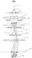
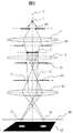
- FIG. 4 shows an observation optical system for the Foucault image of the sample
- FIG. 5 shows an observation optical system for the diffraction pattern of the sample.
- This diffraction pattern observation optical system is an effective optical system for small-angle diffraction observation. This will also be described later.
- the irradiation optical system 4 matches the crossover (11, 13) with the position of the limited field stop 65.
- the position of the limited field stop 65 becomes the diffraction pattern observation position of the sample 3, that is, the reverse space, and the limited field stop 65 can be used as an angle limited stop like the objective stop 55.
- the irradiation optical system is basically operated independently of the imaging optical system for the purpose of controlling the irradiation range of the electron beam for irradiating the sample and the angular spread of the irradiation electron beam.
- the irradiation optical system plays the role of creating a crossover at a precisely defined position below the sample, and the optical system that contributes the action of the irradiation optical system to the imaging optical system Can be considered.
- the first imaging lens 61 When observing the image of the sample, it is imaged by the first imaging lens 61 under the objective lens 5 as shown in FIG.
- the action of the first imaging lens is reduced imaging as in the case of magnetic flux quantum observation.
- An enlarged image of the sample is obtained by the imaging system after the second imaging lens, and the maximum magnification is about 10,000 times in a normal 4-stage imaging optical system (3 imaging lenses + 1 projection lens).
- the limited field stop as an angle limited stop at an appropriate position in the electron diffraction pattern, it is necessary to observe the enlarged diffraction pattern, that is, a large camera length.
- FIG. 5 shows an optical system during diffraction pattern observation.
- the first imaging lens 61 is strongly excited, the position of the limited field stop 65 is expanded, and the optical system propagates to the imaging system after the second imaging lens. It is.
- the distance from the position of the sample 3 to the position of the limited field stop 65 corresponds to the camera length obtained by direct propagation of the electron beam. This distance is approximately 100 to 200 mm with a normal transmission electron microscope, and can be easily magnified (approximately 10,000 times) by the imaging optical system in the subsequent stage, resulting in a large camera length on the order of kilometers. It is possible. This value is 3 to 4 digits larger than the camera length of the conventional transmission electron microscope. That is, the lensless Foucault optical system is an optical system that is also effective for observing small-angle electron diffraction patterns.
- the irradiation optical system since the irradiation optical system is used for the imaging action, the degree of freedom in adjusting the irradiation area on the sample is limited.
- the simplest method as a countermeasure is to select and use an appropriate size for the diaphragm 45 of the irradiation optical system.
- the STEM irradiation diaphragm 44 can be used in a microscope having an objective diaphragm 55 or a scanning transmission electron microscope (STEM) mode. 4 and 5 also show the respective apertures. How to use these apertures will be described in the following examples.
- the irradiation optical system is generally composed of a plurality of electron lenses, but if these electron lens systems are adjusted well, the irradiation area and irradiation angle of the electron beam to the sample can be changed continuously. It is also possible to do.
- a conventional objective aperture can be substituted for the field-of-view limitation to the imaging optical system during diffraction pattern observation (note that it is not an irradiation area).
- the present invention relates to a technique for realizing the Foucault method in a general-purpose transmission electron microscope that does not include an appendage for observing a magnetic domain structure (for example, a magnetic shield lens).
- a magnetic domain structure for example, a magnetic shield lens.
- an electric current is applied.
- the irradiation optical system forms an image of the crossover at the limited field stop position, and the electron beam subjected to the magnetic deflection is selected by the same stop, and the Foucault image is formed by the subsequent image forming optical system. It is a method of imaging and observing. Small-angle diffraction pattern observation and Foucault image observation of the deflected electron beam are realized by changing the focal length of the first imaging lens under the objective lens. Correct with a deflector under the lens.
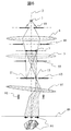
- FIG. 6 shows a typical optical system of the present invention as a first embodiment.
- FIG. 5 is a diagram showing a lensless Foucault optical system similar to that in FIG. 4, except that a deflector 81 is provided below the first imaging lens 61 and that the electron beam transmitted through the first imaging lens 61 is shifted. Is shown to be corrected by the deflector 81.
- the first imaging lens 61 is drawn with an inclination. However, the first imaging lens 61 is not mechanically inclined in this way.
- the deflector is drawn like a small coil, but this is also for the convenience of drawing, and the deflector is a concentric cylindrical magnet with the optical axis as the axis, similar to the conventional deflector.
- the body is composed of a plurality of coils wound around the body so as to sew the same magnetic body as an axis. Then, it is possible to deflect the electron beam in two orthogonal directions within a plane perpendicular to the optical axis. That is, the electron beam can be deflected not only in the left and right directions in the drawing, but also in the direction perpendicular to the drawing.
- the optical system is adjusted with the optical axis of the objective lens as the center and the other lens systems aligned with the optical axis of the objective lens.
- This is an adjustment method that gives the highest priority to the objective lens that has the greatest influence on the image quality of the sample, such as spherical aberration, and the electron microscope used in the present invention is premised on this adjustment. Therefore, when the objective lens is turned off, a deflector is disposed under the first imaging lens so that the optical axis adjustment is performed with priority given to the first imaging lens that forms an image first. This is the center of the optical system adjustment.
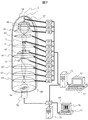
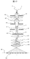
- FIG. 7 is a configuration example of an electron microscope having an optical system for carrying out the present invention. Although it is drawn assuming a general-purpose transmission electron microscope having an acceleration voltage of 100 kV to 300 kV, the components of the electron microscope in the present invention are not limited to those shown in this figure.
- the objective lens 5 is turned off and is drawn with a broken line to show that it is off.
- the electron beam 27 emitted from the electron source 1 is accelerated at a predetermined voltage by the acceleration tube 40 and is irradiated onto the sample 3 by the irradiation optical system (41, 42).
- the crossover for example, in a normal observation method such as high-resolution observation, the crossover (light source image) is connected above the sample, but in the lensless Foucault method, the crossover is connected at the position of the limited field stop 65 below the sample 3. ing.
- Sample 3 is assumed to be a magnetic body having a 180-degree magnetic domain structure, and depicts a state in which the crossover is separated into two spots.
- the deflected electron beam selected / extracted in a specific angle range by the limited field stop 65 is transmitted through the first imaging lens 61, adjusted by the deflector 81 so as to propagate on the optical axis 2, and the subsequent imaging lens After passing through the system (62, 63, 64), the Foucault image 84 is connected to the observation / recording surface 89.
- the diaphragm of the irradiation optical system, the objective diaphragm, the STEM irradiation diaphragm, etc. are not drawn in order to avoid the complexity of illustration. These will be described in later examples.
- the Foucault image 84 formed on the observation / recording surface 89 is acquired as image data through an observation recording medium 79 such as a TV camera or a CCD camera, and is sent to the arithmetic processing unit 75 via the control unit 78 to be sent to the image display device 76. Is output.
- the image data before and after the processing is recorded in the image recording device 77 or the like.
- an observation recording medium 79 a photographic film for an electron microscope can be used, but in this case, digitization processing of image data is required separately.
- TV cameras and CCD cameras have become more common, explanations have been given assuming TV cameras and CCD cameras, but handling of image data is not limited to the configuration shown in FIG.
- control unit 19 of the electron gun the control unit 49 of the acceleration tube, the control unit 48 of the first irradiation lens, the control unit 47 of the second irradiation lens, the control unit 39 such as the fine movement mechanism of the sample, and the control of the objective lens Unit 59, limited field stop control unit 87, first imaging lens control unit 69, deflector control unit 88, second imaging lens control unit 68, third imaging lens control unit 67, projection lens Control unit 66, observation / recording surface 89, observation recording medium 79, observation recording medium control unit 78, arithmetic processing unit 75, image recording unit 77, image display unit 76, control system computer 51 for the entire electron microscope apparatus, control A system monitor 52 and a control system control panel 53 are shown. But the present invention is not limited.
- the actual apparatus includes a deflection system for adjusting the traveling direction of the electron beam, a diaphragm mechanism for limiting the transmission region of the electron beam, and the like.
- these devices are not shown in FIG. 7 because they are not directly related to the present invention. 7 is assembled in the vacuum vessel 18 and continuously evacuated by a vacuum pump, the vacuum evacuation system is not directly related to the present invention, and thus will be omitted. Such omission is the same in any figure of the present application as necessary.
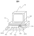
- FIG. 8 shows an example of a control panel of the control system used in the present invention.
- a sample fine movement knob two horizontal directions of X and Y directions: 531X, 531Y
- a magnification adjustment knob 532 for adjusting magnification of X and Y directions
- an irradiation area adjustment knob 533 for adjusting magnification of X and Y directions
- an irradiation system deflection adjustment knob 534 for controlling the focus adjustment knob 535.
- Etc. are arranged. These are frequently used when operating an electron microscope. Even an electron microscope controlled by a control computer is installed on a control panel in order to reduce the operation load on the operator.
- the control panel 53 includes an irradiation optical system adjustment stop means 539 and its stop release means 538.
- the irradiation optical system In the lensless Foucault method, as described above, the irradiation optical system must be used to bind the crossover to the position of the aperture on the lower side of the sample (a limited field aperture in a conventional electron microscope). For this reason, after the conditions of the imaging optical system are determined, the irradiation optical system must not be fixed and changed in the same manner as the imaging optical system. However, in a normal electron microscope, as described above, the irradiation optical system can be operated independently and with priority from other operations in order to adjust the irradiation region, irradiation angle, etc.
- the irradiation optical system is often operated erroneously, and the entire optical system must be adjusted again.
- a means for stopping the change of the irradiation optical system by a simple operation and restarting the adjustment of the irradiation optical system stopped by the next operation is provided.
- the operator of the electron microscope can perform observation by the lensless Foucault method without any special burden.
- the irradiation optical system adjustment stop means 539 and the stop release operation means 538 are depicted as operation parts each having a button shape, but the operation method and the operation part shape are not limited thereto.
- FIG. 9 shows an example different from Example 2 of the control panel 53 of the control system used in the present invention.
- the shape of the control panel 53, the other control knobs (531X, 531Y, 532, 533, 534, 535) including the adjustment stop means 539 of the irradiation optical system and the stop release operation means 538 are the same as those in FIG.
- FIG. 9 shows a state in which an observation mode switching knob is added on the control panel 53.
- On the control panel 53 of the conventional electron microscope means for constructing an optical system corresponding to each observation purpose by simple operations such as an image observation mode, a low magnification image observation mode, and a diffraction pattern observation mode (in order of 527). 528, 529).
- control panel 53 constructs an optical system for the Foucault image observation mode 536 in the lensless Foucault method and an optical system for the small-angle diffraction pattern observation mode. Means 537 are added.
- the two optical systems shown in FIGS. 4 and 5 can be switched by a simple operation. In this case, it goes without saying that the propagation of the electron beam is adjusted by the deflector along the optical axis in each mode.
- the installation of means for switching between the Foucault image observation mode and the small-angle diffraction pattern observation mode allows the electron microscope operator to perform observation by the lensless Foucault method without any special burden.
- the means 536 for constructing an optical system for the Foucault image observation mode and the means 537 for constructing an optical system for the small-angle diffraction pattern observation mode are drawn as operation parts each having a button shape. However, it is not limited to this operation method and the shape of the operation unit.
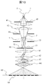
- FIG. 10 shows the entire optical system of an electron microscope as an example of the Foucault image observation mode
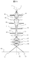
- FIG. 11 shows the entire optical system of an electron microscope as an example of the small-angle diffraction pattern observation mode.
- the upper part from the first imaging lens 61 is the same as that in FIGS. 4 and 5, respectively.
- the electron lens (62, 63, 64) downstream from the second imaging lens 62 An optical system aperture 45, an STEM illumination aperture 44, an objective aperture 55, and a limited field aperture 65 are specified.
- the switching of the optical system by the mode switching described in the third embodiment corresponds to the switching between FIG. 10 and FIG.
- the lens mainly responsible for mode switching is the first imaging lens
- the lens primarily responsible for magnification or camera length is the third imaging lens, so what happens when the mode is switched? It is necessary to select an appropriate magnification and camera length, that is, to determine conditions for the third imaging lens. Therefore, in the present invention, control is performed so as to return to the last magnification when the mode was observed last time or the last camera length. Then, the magnification and the camera length are newly corrected from the returned original state to values suitable for the observation state at that time. Such an operation is repeated to finally reach an observation condition desired by the operator.
- Each lens condition, deflector operating condition, etc. in the above mode are stored in the control system computer, and the previous or past operating conditions can be immediately reproduced as necessary.
- FIGS. 10 and 11 show a state in which the diaphragm 45 of the irradiation optical system defines an electron beam irradiation area for the sample 3. That is, in the mode switching described above, the basic control is that the aperture 45 of the irradiation optical system does not change its position or hole diameter.
- the other imaging lens is responsible for this, not the first imaging lens responsible for the mode change.
- the optical system configuration is handled by the three imaging lenses.
- the operating conditions of all magnifications, all lenses at each camera length, and all deflectors are stored in memory, and in each case, the corresponding lens data can be read out to construct an optical system.
- the observation direction is changed by exchanging the sample or tilting the sample, the condition stored in advance is deviated. This shift is finely adjusted by the first imaging lens in the operation stage of adjusting the optical system first.
- the lens condition of the first imaging lens that is, the focal length is not changed.
- the lens conditions of other imaging lenses such as the third imaging lens
- the conditions of the first imaging lens also need to be corrected, but this is determined to be a minute amount.
- the focal length of another imaging lens such as a lens
- the focus adjustment knob on the control panel shown in FIGS. 8 and 9 is a knob that controls the focus of the sample image and the focus of the diffraction pattern of the sample, but the actually controlled electronic lens is the mode. It depends on. For example, in the image observation mode, the focal length of the objective lens is changed, whereas in the low magnification image observation mode, the focal length of the first imaging lens or the second imaging lens (by the optical system) is changed. In the diffraction pattern observation mode, the focal length of the first imaging lens is changed. This is because the control panel is used with the meaning of “focus adjustment on the object being viewed”, and the electron microscope operator is not aware of which lens to adjust, and is not looking at the object (image or The adjustment can be performed only on the diffraction pattern.
- the first imaging lens can be operated by the focus adjustment knob in the Foucault image observation mode and the first imaging lens in the small-angle diffraction pattern observation mode.
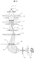
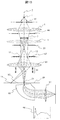
- FIG. 12, FIG. 13, FIG. 14 and FIG. 15 show the use of the apparatus when the energy analyzer is used in combination in the Foucault image observation mode or the small angle diffraction mode in the present invention.
- an energy analyzer an electron energy loss spectrometer (EELS) is assumed.
- EELS electron energy loss spectrometer
- the method of the present invention can be implemented as long as it can be used in combination with a transmission electron microscope. ) Is not limited.
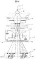
- FIG. 12 shows a state in which an electron beam forming the Foucault image 84 is introduced into the EELS 95 and the energy spectrum 98 of the electron beam is measured.
- An energy spectrum 98 is obtained only by an electron beam having a specific deflection angle. That is, for example, when an element in a specific magnetic domain having an action of deflecting an electron beam in a certain direction is segregated, the element type and the fact of segregation can be known. This method makes it possible to measure the spectrum for each magnetic domain, and to obtain knowledge about the relationship between the magnetic domain structure and the element distribution.
- FIG. 12 shows an optical system introduced into EELS after forming a Foucault image with an electron microscope.
- FIG. 13 is the same as FIG. 12 in that the electron beam that forms the Foucault image 84 is introduced into the EELS 95 after the Foucault image 84 is formed.
- an image of energy loss electrons using the electron optical system 97 of the EELS is used.
- 99 is an example of observing 99. After visualizing the deflection angle of the electron beam in the Foucault optical system, the energy distribution of the electron beam is visualized. That is, not only the magnetic domain structure but also the distribution density of segregated elements in the magnetic domain is visualized.
- FIG. 14 shows an example in which an electron beam that has not been deflected is formed as a Foucault image 85 and then introduced into EELS 95 to observe an image 96 due to energy-loss electrons.
- an electron beam that has not been deflected is formed as a Foucault image 85 and then introduced into EELS 95 to observe an image 96 due to energy-loss electrons.
- the particle when there is a non-magnetic particle in the sample 3, not only can the particle be identified as the Foucault image 85, but the element spectrum in the particle from the energy spectrum 98 and the non-magnetic image 96 from the image of energy loss electrons. Knowledge about the distribution of specific elements in grains can be obtained.
- FIG. 15 shows an example in which a specific diffraction spot (crossover 11 in FIG. 15) is introduced into the EELS 95 after forming a small-angle diffraction pattern 82 with an electron microscope.
- the energy spectrum 98 is illustrated as an example, but the image 99 due to energy-loss electrons can be observed by using the EELS electron optical system 97.
- the obtained knowledge and its features are the same as those described with reference to FIGS.
- a state in which the deflector 81 is operated in order to capture the diffraction spots (11, 13 and the like) in the diffraction pattern 82 into the EELS 95 is shown.
- the deflector 81 has a two-stage structure different from that shown in FIG. 6, the present invention is not limited to this.
- the combined use of the lensless Foucault method and the energy analyzer described with reference to FIGS. 12 to 15 differs depending on the object to be observed / measured and the deflection angle distribution at that time and the combination of the optical system used.
- An optimal combination of experiments may be performed according to the experimental conditions.
- FIG. 16 shows an example of the entire optical system of the electron microscope different from FIG. 10 in the Foucault image observation mode. 16 is the same as FIG. 10 in that the irradiation range of the sample 3 by the electron beam is determined by the diaphragm 45 of the irradiation optical system, but the electron beam that connects the crossover (11, 13) after passing through the sample. Is different from FIG. 10 in that the spatial range is defined by the objective aperture 55. In the case of FIG. 16, the objective aperture 55 performs the same function as the limited field stop in the case of a normal electron microscope.
- the spatial range of the electron beam introduced into the imaging lens system (61, 62, 63, 64) at the latter stage of the sample for example, an electron beam in a range that is greatly affected by aberrations or that does not require observation is used. It is possible to eliminate it in advance or use it. Since the spatial range limitation of these electron beams can be performed completely independently of the electron beam irradiation to the sample 3, the electron beam sample irradiation conditions do not change. For this reason, the control of the observation condition by changing the objective aperture 55 does not cause a new sample drift or the like.
- FIG. 17 shows an example of the entire optical system of the electron microscope different from FIG.
- FIG. 17 shows an example of controlling a spatial range of an irradiation electron beam using a STEM irradiation diaphragm 44 positioned between the irradiation optical system (41, 42) and the sample 3 in a transmission electron microscope having an STEM mode. It is.
- the STEM irradiation diaphragm 44 can directly control the amount and range of the electron beam that irradiates the sample 3, which is effective for controlling the electron beam irradiation amount in the lensless Foucault method, for example, when observing a biological sample. Aperture. If used together with the diaphragm 45 of the irradiation optical system, the irradiation range can be changed in detail.
- Non-Patent Document 2 In general, in electron beam holography, a limited field stop and an electron beam biprism are often used together or exchanged. That is, also in the present invention, it is possible to dispose the electron biprism at a position (a position of the limited field stop) where a crossover (light source image) is formed by the irradiation optical system. Thereby, even in an optical system that does not use an objective lens, the Twin Foucault method (Patent Document 1) (Non-Patent Document 2) can be implemented. Electron beam holography and electron beam biprism are described in Patent Document 1, Non-Patent Document 2, and Non-Patent Document 3.
- FIG. 18 shows an optical system for carrying out the Twin Foucault method in the present invention. Rather than selecting the electron beam that has passed through the sample 3 and has been deflected by using the limited field stop, the electron biprism 9 further applies deflection or suppresses the deflection so that the observation / recording surface 89 is
- This is an optical system that individually images electron beams deflected by the sample 3 at different positions. That is, two Foucault images (841, 842) are observed at a time.
- FIG. 18 shows an example in which a negative voltage is applied to the filament electrode 91 of the electron biprism 9 as an example, but the applied voltage may be positive or negative.
- the Twin Foucault method is an observation method based on a new concept of observing one mirror and two images, but this can also be implemented in the present invention.
- the electron microscope used is a general-purpose HF-3300 transmission type high resolution electron microscope (acceleration voltage 300 kV) manufactured by Hitachi High-Tech. 4 and 5, or if including the deflection system for adjusting the optical axis, adjustment was made so that FIGS. 6 and 5 can be switched by one operation. That is, the sample image observation mode and the sample diffraction pattern observation mode were adjusted to be switched with a single operation with high reproducibility. Moreover, when noting all the electron lens systems, FIG. 9, FIG. 10 corresponds to this.
- the observed sample is a thin film of manganese oxide-based material La 0.75 Sr 0.25 MnO 3 (LSMO), and it is known that it forms twins, has a 180 ° inversion domain structure, and a 90 ° domain structure. It has been.
- LSMO manganese oxide-based material La 0.75 Sr 0.25 MnO 3
- Fig. 19 shows the Fresnel image of LSMO.
- A is an underfocus (underfocus) image
- B is an infocus (normal focus) image
- C is an overfocus (overfocus) image.
- a linear contrast 72 seen at the boundary between the band-like regions in FIGS. 19A and 19C is a domain wall. It can be seen that the linear contrast 72 of the same portion is inverted between the A underfocus image and the C overfocus image. Further, the linear contrast 72 is inverted at the adjacent boundary portion in FIG. 19A or the adjacent boundary portion in FIG. 19C. It can be seen that the contrast 72 of the Fresnel image of these domain walls changes depending on the focus and the arrangement of the magnetic domains. That is, the details are as described in FIGS.
- FIG. 19 for example, a streaky black stripe pattern is seen vertically in the center of the figure through A to C in FIG. 19, which is an isotropic interference fringe, and the sample thin film is a crystal and has a Bragg angle. Contrast due to the degree of distortion. The equiangular interference fringes are broken, which indicates that the broken portion is a twin boundary. From the above observation results, it can be seen that the domain wall is along the twin boundary. Thus, also in the present invention, it is easy to visualize the domain wall by the Fresnel method.
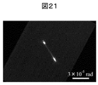
- FIG. 20 shows an example of observation of a Foucault image (in-focus) at the same location as FIG. 19, and FIG. 21 shows a small-angle electron diffraction pattern used when constructing the Foucault image of FIG.
- the camera length is about 150 m, which is an enlarged image of about 200 times that of the normal Bragg diffraction pattern observation. Therefore, note that the angular scale in the diffraction pattern is also 10 -5 rad.
- FIG. 21 In the small angle diffraction pattern of FIG. 21, the diffraction spot is separated into two while pulling a streak. Since this streak is linear, it can be seen that the 180 ° reversal domain boundary is a Bloch domain wall. 20A is a Foucault image observed from the upper left diffraction spot in FIG. 21, and FIG. 20B is a Foucault image observed from the lower right diffraction spot. It can be seen that the contrasts (71, 73) are inverted at the twin boundaries, respectively, and a 180 ° inverted magnetic domain structure in which the magnetic domains are alternately replaced is obtained.
- FIG. 22 shows a Fresnel image of a 90/180 degree magnetic domain structure and a small-angle electron diffraction pattern.
- a zigzag domain wall is observed in the vertical direction in the center of each of FIGS. 22A (under focus) and B (over focus). This is a 180-degree domain wall, and is a line extending left and right from each vertex of the zigzag domain wall.
- the contrast of the shape is a 90-degree domain wall.
- the small angle diffraction patterns in the observation regions of FIGS. 22A and 22B are FIG. 22C.
- a streak that intersects the center of the diffraction pattern in an X shape is due to the 180-degree domain wall, and a streak that connects the left and right diffraction spots in the vertical direction is due to the 90-degree domain wall.
- FIG. 23 shows a Foucault image of a 90-degree domain wall and a streak in a small-angle diffraction pattern selected when the Foucault image is obtained.
- FIG. 23A is a Foucault image of the 180-degree domain wall of the X-shaped streak at the center of the diffraction pattern
- FIG. 23B is a Foucault image of the 90-degree domain wall of the left streak of the diffraction pattern
- FIG. In the Foucault image of FIG. 23, only the domain wall is visualized linearly. Depending on the streak to be selected, the domain wall to be visualized is different, and it is possible to observe a specific domain wall.
- the domain wall can be observed directly in focus according to the method of the present invention. Furthermore, if elemental analysis can be performed with an energy analyzer while confirming the Foucault image of the domain wall, the element segregated on the domain wall can be known.
- Electron source or electron gun 10 ... Electron source image (crossover), 11 ... Electron source image or electron diffraction spot deflected leftward on the paper surface by the sample, 13 ... Deflection rightward on the paper surface by the sample Image of electron source or electron diffraction spot, 18 ... Vacuum container, 19 ... Control unit of electron source, 2 ... Optical axis, 24 ... Projection plane, 25 ... Intensity distribution of electron beam on projection plane, 27 ... Electron beam Or, the trajectory of the electron beam, 3 ... sample, 31 ⁇ 33 ... magnetic domain, 32 ... domain wall, 35 ... focus position below the sample, 36 ... focus position above the sample, 39 ...
- control unit of the sample 4 ... irradiation optical system ( Lens system), 40 ... accelerator tube, 41 ... first irradiation lens, 42 ... second irradiation lens, 44 ... STEM irradiation diaphragm, 45 ... irradiation optical system diaphragm, 47 ... second irradiation lens control unit, 48 ... First irradiation lens 49 ... Acceleration tube control unit, 5 ... Objective lens, 51 ... Control system computer, 52 ... Control system computer monitor, 527 ... Image observation mode means, 528 ... Low magnification image observation mode means, 529 ...
- Diffraction Pattern observation mode means 53 Control system control panel, 531X: X direction sample fine adjustment knob, 531Y: Y direction sample fine adjustment knob, 532: Magnification adjustment knob, 533 ... Irradiation area adjustment knob, 534 ... Irradiation system deflection adjustment knob, 535... Focus adjustment knob 536.
- ... objective lens control unit 61 ... first imaging lens, 62 ... second imaging lens, 63 ... third Imaging lens, 64 ... projection lens, 65 ... restricted field stop, 66 ... projection lens control unit, 67 ...
- third imaging lens control unit 68 ... second imaging lens control unit, 69 ... first connection Image lens control unit 71, 73 ... Magnetic domain image, 72 ... Domain wall image, 75 ... Arithmetic processing device, 76 ... Image display device, 77 ... Image recording device, 78 ... Observation recording medium control unit, 79 ... Observation Recording medium, 8: Image surface of sample by objective lens, 81: Deflector, 82: Diffraction pattern, 84: Foucault image, 85: Image by electron beam not deflected by sample, 86: Fresnel image, 87: Restricted field of view Diaphragm control unit, 88 ... Deflector control unit, 89 ... Observation / recording surface, 9 ...
- Electron biprism 91 ... Electron biprism filament electrode, 95 ... EELS, 96 ... Deflection by sample Image of energy-loss electrons not subjected to orientation, 97 ... EELS electron optical system, 98 ... energy spectrum, 99 ... image of energy-loss electrons deflected by sample
Landscapes
- Chemical & Material Sciences (AREA)
- Analytical Chemistry (AREA)
- Crystallography & Structural Chemistry (AREA)
- Physics & Mathematics (AREA)
- Health & Medical Sciences (AREA)
- Life Sciences & Earth Sciences (AREA)
- Biochemistry (AREA)
- General Health & Medical Sciences (AREA)
- General Physics & Mathematics (AREA)
- Immunology (AREA)
- Pathology (AREA)
- Analysing Materials By The Use Of Radiation (AREA)
Abstract
Description
図1は180度反転磁区構造を有する磁性試料で電子線が偏向を受ける様子を示したものである。電子線が偏向される角度は、磁化の大きさと試料の厚さに依存する。したがって、厚さが一定で磁化が均一な試料の場合、電子線の受ける偏向はどの領域でも角度が同じで、磁区構造に伴って方位・方向が異なることになる。図1に示すごとく、180度反転磁区構造を有する試料3に電子線27が入射すると、試料3を透過した電子線27は、それぞれの磁区(31、33)で逆方向に偏向を受ける。偏向を受けた電子線27は、試料下方に十分な距離だけ伝播すると、投影面24上において、180度磁壁32に該当する位置で互いに重なりあう状況と、逆に互いに離れる状況が発生する。この投影面24上での電子線の強度の粗密を結像するのがフレネル法である。図1の下部に投影面上での電子線の強度分布のグラフ25を例示する。
図3は、フーコー法による磁区構造観察の光学系である。図1と同様に180度反転磁区構造を有する試料3を透過した電子線は、それぞれの磁区(31、33)で互いに逆方向に偏向を受け、その方向に偏向を受けた電子線は、例えば対物レンズ5の後焦点面54(厳密には対物レンズによる光源の像面)で、その偏向角度に応じた位置にスポット(11、13)を結ぶ。そこで、対物絞り55を挿入し、観察したい磁区を透過した電子線のみを選択し像面7上に結像させる。例えば図3Aでは、磁区31を透過し紙面上左方向に偏向された電子線を選択した例であり、図3Bは逆に磁区33を透過し、紙面上右方向に偏向された電子線を選択した例である。いずれにしても、選択された磁区が白色、選択されなかった磁区が黒色(電子線が来ない)で観察され、180度反転磁区構造の場合、それぞれの磁区(31、33)がストライプ状(71、73)のフーコー像84として可視化される。
つい最近、磁気シールドレンズを備えない通常の汎用型透過電子顕微鏡を用いてフーコー法、および小角電子回折を実施可能とする手法が開発された(非特許文献3)。レンズレス・フーコー法である。ここで言う『レンズレス』とは、対物レンズをオフとして、結像に用いないという意味である。この手法の詳細については後述する。(なお、本発明は、レンズレス・フーコー法を実施するに当り、電子顕微鏡操作者の装置操作上の負担を軽減し、効果的な実験を実施するために成されたもので、レンズレス・フーコー法での光学系の制御に関するものである。)
上述のローレンツ顕微鏡法以外に、電子線の位相分布から、試料の磁区構造などを観察する手法として、電子線ホログラフィー(非特許文献4)や強度輸送方程式法(非特許文献5)などが開発されている。いずれの手法もそれぞれ利点を有しているが、電界放出型電子線など干渉性の高い電子線が必要である上、電子線ホログラフィーでは付加装置として電子線バイプリズムが必要であり、試料形状には参照波を透過させるための領域を考慮しなければならないこと、強度輸送方程式法ではインフォーカスを挟んで少なくとも2枚のデフォーカス量が既知の画像(都合3枚の画像)が必要であり、各像の倍率、位置合わせなどの調整処理が不可欠であること、など、実施に当って煩雑さも多いのが実情である。
最近、試料中磁化による電子線の偏向角度を、回折面で回折スポットとして観察する手法が実施され始めた(非特許文献6)。この手法は電子線の小さな偏向角度を回折面で回折パターンとして(すなわち、大カメラ長の回折パターンとして)観察する手法で、1960年代に実施されていたが(非特許文献7)、その後長く忘れられた技術であった。平均的な偏向角度の情報を得るには有効な手法で、磁性素子の微細化・薄膜化などにより電子線の偏向角度が小さくなったとき、個別の素子による透過電子の微小な偏向角度を検出するよりも、平均的ではあるが電子線の照射領域全体から受ける透過電子線の偏向角度を回折面で検出する方法として見直されているものである。

上記、フーコー法を最適に実施するためには、回折面で角度制限絞りを適切に用いる必要がある。例えば、加速電圧300 kVの電子線で容易に透過可能な50 nmの厚さの磁性材料(磁化1T(テスラ))の場合、磁気による偏向角度はおよそ2×10⁻⁵ radとなり、結晶によるブラッグ回折角よりも3桁近くも小さな角度となる。そのためフーコー法では、その結像精度を上げるためには、自ずから小角回折法が実現できなければならない。すなわち、小角回折に対応した大カメラ長の回折パターンとなる様に光学系を構築する(回折パターンを拡大できる光学系とする)必要がある。その上で、回折パターンの回折面と角度制限絞りの挿入面が一致している必要がある。
レンズレス・フーコー法は、ローレンツ電子顕微鏡による磁気シールド対物レンズを用いることなく、汎用型電子顕微鏡を用いてフーコー法を実現できる光学系として開発されたものである。通常のフーコー法では、磁気シールド対物レンズにより試料を透過した電子線のクロスオーバーが対物絞り面上に結像され、電子線の偏向角度分離は対物絞り孔のサイズ、挿入位置によって制御される。一方、レンズレス・フーコー法においては、対物レンズはオフとし(したがって、試料は磁場に浸漬されない)、対物レンズに代わって照射光学系によって通常の場合の制限視野絞り面(通常の場合の対物レンズによる試料の像面)に、試料を透過した電子線のクロスオーバーを結像させる。そして、制限視野絞りを用いて、電子線の偏向角度分離を実施する。回折パターンを観察するための結像系の使用方法は、通常の場合の試料像を観察する時と同じであり、試料の像を観察する場合は、結像光学系に属するレンズのいずれかの使用条件を弱励磁として試料の像にフォーカスを合わせる。これら2つの光学系を図4と図5に示す。図4は試料のフーコー像の観察光学系、図5は試料の回折パターンの観察光学系である。なお、この回折パターン観察光学系は小角回折観察に有効な光学系である。これについても後述する。
Claims (16)
- 電子線の光源と、前記光源から放出される電子線を試料に照射するための複数の電子レンズから構成される照射光学系と、前記試料への前記電子線の照射量を変更する照射光学系に属する移動可能な照射絞りと、前記電子線が照射する前記試料を保持するための試料保持装置と、前記試料の像もしくは前記試料の回折パターンを結像するための複数の電子レンズから構成される結像レンズ系と、前記結像レンズ系による前記試料の像もしくは前記試料の回折パターンを観察する観察面と、前記試料の像もしくは前記試料の回折パターンを記録するための記録装置と、を有する電子顕微鏡であって、
前記結像レンズ系に属する電子レンズのうち前記電子線の進行方向最上流に位置する第1の結像レンズと前記試料保持装置との間に前記試料を透過した電子線の一部を選択透過させるための移動可能な第1の絞り孔を備え、
前記第1の結像レンズの前記電子線の進行方向下流側に前記電子線を偏向させるための偏向装置を備え、
前記照射光学系により前記絞り孔に前記試料を透過した電子線を収束させ、
前記第1の結像レンズの焦点距離の変更に伴って発生する前記電子線の軸ずれを前記偏向装置によって補正し、
前記第1の結像レンズの焦点距離を変更することによって前記試料の像と前記試料の回折パターンを観察する、
ことを特徴とする電子顕微鏡。 - 前記照射光学系に属する電子レンズのうち前記試料への前記電子線の照射領域の変更を担う電子レンズの状態が、該電子顕微鏡の操作者による操作によって固定されるとともに、前記操作もしくは前記操作とは別なる操作によって解除されるまで、該電子顕微鏡の他の操作によらず該電子レンズの状態が継続されることを特徴とする請求項1に記載の電子顕微鏡。
- 前記試料の像を観察する前記第1の結像レンズの焦点距離と、前記試料の回折パターンを観察する前記第1の結像レンズの焦点距離と、が該電子顕微鏡の操作者による前記請求項2に記載の操作とは別なる操作によって切り替えられることを特徴とする請求項1もしくは2に記載の電子顕微鏡。
- 請求項3に記載の操作によって前記試料の像の観察と前記試料の回折パターンの観察とが切り替えられる際に、前記試料像の観察に要した前記偏向装置を含む前記結像レンズ系の状態と、前記試料回折パターンの観察に要した前記偏向装置を含む前記結像レンズ系の状態と、がそれぞれ記録され、前記切り替え操作により、それぞれの観察における前回観察の最後の状態に復することを特徴とする請求項3に記載の電子顕微鏡。
- 請求項3に記載の操作によって前記試料の像の観察と前記試料の回折パターンの観察とが切り替えられる際に、前記照射絞りが移動しないことを特徴とする請求項3に記載の電子顕微鏡。
- 前記結像レンズ系に属する電子レンズの内、前記第1の結像レンズ以外の電子レンズのいずれかの状態を変更させる際、前記第1の結像レンズの焦点距離が変更されないことを特徴とする請求項1に記載の電子顕微鏡。
- 前記試料の回折パターンの観察を行なう状態の時に、該電子顕微鏡の操作パネル上にあってFOCUSと明記されているなどの方法により試料の像あるいは試料の回折パターンのフォーカスを調整する意図で備え付けられたつまみなどを操作することによって、前記第1の結像レンズの焦点距離を変更できることを特徴とする請求項1から6のいずれかに記載の電子顕微鏡。
- 前記偏向装置が、前記電子線を前記電子顕微鏡の光軸に垂直な平面上の直交する2方向に偏向可能であることを特徴とする請求項1から7のいずれかに記載の電子顕微鏡。
- 前記第1の結像レンズの焦点距離の変更と前記偏向装置による前記電子線の軸ずれの補正とが連動するように構成されていることを特徴とする請求項1から8のいずれかに記載の電子顕微鏡。
- 前記試料の像もしくは前記試料の回折パターンの一部もしくは全部を成す電子線をエネルギー分析器に導入し、エネルギースペクトルを計測することを特徴とする請求項1から9のいずれかに記載の電子顕微鏡。
- 前記試料の像もしくは前記試料の回折パターンの一部もしくは全部を成す電子線をエネルギー分析器に導入し、エネルギー分光された試料像もしくは回折パターンを得ることを特徴とする請求項1から9のいずれかに記載の電子顕微鏡。
- 前記試料保持装置と前記第1の絞り孔との間に前記結像レンズ系に入射する電子線を制限するための移動可能な第3の絞り孔が設置されることを特徴とする請求項1から11のいずれかに記載の電子顕微鏡。
- 前記試料保持装置と前記照射光学系との間に前記電子線が試料を照射する領域を制限するための移動可能な第2の絞り孔が設置されることを特徴とする請求項1から12のいずれかに記載の電子顕微鏡。
- 前記第1の絞り孔が設置される位置に光軸と垂直に電子線バイプリズムが配置されることを特徴とする請求項1から13のいずれかにに記載の電子顕微鏡。
- 電子線の光源と、前記光源から放出される電子線を試料に照射するための複数の電子レンズから構成される照射光学系と、前記試料への前記電子線の照射量を変更する照射光学系に属する移動可能な照射絞りと、前記電子線が照射する前記試料を保持するための試料保持装置と、前記試料の像もしくは前記試料の回折パターンを結像するための複数の電子レンズから構成される結像レンズ系と、前記結像レンズ系による前記試料の像もしくは前記試料の回折パターンを観察する観察面と、前記試料の像もしくは前記試料の回折パターンを記録するための記録装置と、前記結像レンズ系に属する電子レンズのうち前記電子線の進行方向最上流に位置する第1の結像レンズと前記試料保持装置との間に前記試料を透過した電子線の一部を選択透過させるための移動可能な絞り孔と、前記第1の結像レンズの前記電子線の進行方向下流側に前記電子線を偏向させるための偏向装置と、を備える電子顕微鏡が実行する試料像もしくは回折パターンの観察法であって、
前記照射光学系により前記絞り孔に前記試料を透過した電子線を収束させ、
前記第1の結像レンズの焦点距離の変更に伴って発生する前記電子線の軸ずれを前記偏向装置によって補正し、
前記第1の結像レンズの焦点距離を変更することによって前記試料の像と前記試料の回折パターンを観察する、
ことを特徴とする試料像もしくは回折パターンの観察法。 - 電子線の光源と、前記光源から放出される電子線を試料に照射するための複数の電子レンズから構成される照射光学系と、前記試料への前記電子線の照射量を変更する照射光学系に属する移動可能な照射絞りと、前記電子線が照射する前記試料を保持するための試料保持装置と、前記試料の像もしくは前記試料の回折パターンを結像するための複数の電子レンズから構成される結像レンズ系と、前記結像レンズ系による前記試料の像もしくは前記試料の回折パターンを観察する観察面と、前記試料の像もしくは前記試料の回折パターンを記録するための記録装置と、前記結像レンズ系に属する電子レンズのうち前記電子線の進行方向最上流に位置する第1の結像レンズと前記試料保持装置との間に前記試料を透過した電子線の一部を選択透過させるための稼動可能な絞りと、前記第1の結像レンズの前記電子線の進行方向下流側に前記電子線を偏向させるための偏向装置と、を備える電子顕微鏡が実行するエネルギースペクトル計測法であって、
前記照射光学系により前記絞り孔に前記試料を透過した電子線を収束させ、
前記第1の結像レンズの焦点距離の変更に伴って発生する前記電子線の軸ずれを前記偏向装置によって補正し、
前記第1の結像レンズの焦点距離を変更することによって前記試料の像と前記試料の回折パターンを観察するとともに、
前記試料の像もしくは前記試料の回折パターンの一部もしくは全部を成す電子線をエネルギー分析器に導入することによってなされるエネルギースペクトル計測法。
Priority Applications (3)
| Application Number | Priority Date | Filing Date | Title |
|---|---|---|---|
| US14/916,529 US9679738B2 (en) | 2013-09-30 | 2014-05-16 | Electron microscope |
| CN201480047309.4A CN105531793B (zh) | 2013-09-30 | 2014-05-16 | 电子显微镜 |
| DE112014003760.5T DE112014003760B4 (de) | 2013-09-30 | 2014-05-16 | Elektronenmikroskop und Beobachtungsverfahren |
Applications Claiming Priority (2)
| Application Number | Priority Date | Filing Date | Title |
|---|---|---|---|
| JP2013202951A JP6173862B2 (ja) | 2013-09-30 | 2013-09-30 | 電子顕微鏡 |
| JP2013-202951 | 2013-09-30 |
Publications (1)
| Publication Number | Publication Date |
|---|---|
| WO2015045476A1 true WO2015045476A1 (ja) | 2015-04-02 |
Family
ID=52742635
Family Applications (1)
| Application Number | Title | Priority Date | Filing Date |
|---|---|---|---|
| PCT/JP2014/063016 Ceased WO2015045476A1 (ja) | 2013-09-30 | 2014-05-16 | 電子顕微鏡 |
Country Status (5)
| Country | Link |
|---|---|
| US (1) | US9679738B2 (ja) |
| JP (1) | JP6173862B2 (ja) |
| CN (1) | CN105531793B (ja) |
| DE (1) | DE112014003760B4 (ja) |
| WO (1) | WO2015045476A1 (ja) |
Cited By (3)
| Publication number | Priority date | Publication date | Assignee | Title |
|---|---|---|---|---|
| CN110730923A (zh) * | 2017-05-05 | 2020-01-24 | 卡尔蔡司显微镜有限责任公司 | 确定光学系统的可互换部件的情境信息 |
| WO2020022469A1 (ja) | 2018-07-26 | 2020-01-30 | 国立研究開発法人理化学研究所 | 電子顕微鏡およびそれを用いた試料観察方法 |
| JP7592956B2 (ja) | 2019-07-25 | 2024-12-03 | エフ イー アイ カンパニ | ローレンツem用補正器転送光学系 |
Families Citing this family (13)
| Publication number | Priority date | Publication date | Assignee | Title |
|---|---|---|---|---|
| JP2017016755A (ja) * | 2015-06-29 | 2017-01-19 | 株式会社日立ハイテクノロジーズ | 荷電粒子線装置 |
| KR101785034B1 (ko) * | 2015-09-09 | 2017-10-12 | 광주과학기술원 | 라인 빔을 사용한 레이저 검지 장치 및 이를 이용한 차량정보 인식 방법 |
| CN105869491B (zh) * | 2016-05-17 | 2018-07-10 | 北京理工大学 | 一种透射电镜教学模型的装置 |
| CN108036739B (zh) * | 2017-11-17 | 2020-01-21 | 宁波大学 | 一种基于移动光阑的显微三维测量系统及方法 |
| FR3073956B1 (fr) * | 2017-11-22 | 2019-12-27 | Commissariat A L'energie Atomique Et Aux Energies Alternatives | Methode d'acquisition d'hologrammes par holographie electronique hors axe optique en mode precession |
| EP3489989B1 (en) * | 2017-11-27 | 2020-07-08 | FEI Company | Transmission charged particle microscope with adjustable beam energy spread |
| JP7228869B2 (ja) * | 2018-02-23 | 2023-02-27 | 国立大学法人 東京大学 | 電子顕微鏡及び測定試料の観察方法 |
| EP3550585B1 (en) * | 2018-04-05 | 2021-06-23 | FEI Company | Studying dynamic specimens in a transmission charged particle microscope |
| CN108508047B (zh) * | 2018-06-16 | 2023-11-21 | 金华职业技术学院 | 一种原子束显微装置 |
| EP3648138A1 (en) * | 2018-10-31 | 2020-05-06 | FEI Company | Measurement and endpointing of sample thickness |
| JP7244829B2 (ja) * | 2019-02-22 | 2023-03-23 | 株式会社日立製作所 | 干渉電子顕微鏡 |
| US11101101B2 (en) * | 2019-05-15 | 2021-08-24 | Fei Company | Laser-based phase plate image contrast manipulation |
| CN113555267A (zh) * | 2021-06-22 | 2021-10-26 | 纳境鼎新粒子科技(广州)有限公司 | 电子显微镜系统 |
Citations (5)
| Publication number | Priority date | Publication date | Assignee | Title |
|---|---|---|---|---|
| JPH04137344A (ja) * | 1990-09-27 | 1992-05-12 | Jeol Ltd | フーコー電子顕微鏡 |
| JP2010540895A (ja) * | 2007-09-25 | 2010-12-24 | サントル ナショナル ドゥ ラ ルシェルシュ シアンティフィク | ナノスケール変形を測定する方法、デバイス及びシステム |
| JP2011040217A (ja) * | 2009-08-07 | 2011-02-24 | Hitachi Ltd | 透過型電子顕微鏡およびそれを用いた試料像の観察方法 |
| JP2012199022A (ja) * | 2011-03-18 | 2012-10-18 | Osaka Prefecture Univ | 電子顕微鏡、および回折像観察方法 |
| WO2013046277A1 (ja) * | 2011-09-30 | 2013-04-04 | 株式会社日立製作所 | 電子顕微鏡および試料観察方法 |
Family Cites Families (7)
| Publication number | Priority date | Publication date | Assignee | Title |
|---|---|---|---|---|
| JPS60220541A (ja) | 1984-04-17 | 1985-11-05 | Jeol Ltd | 透過電子顕微鏡 |
| US4851677A (en) * | 1984-12-07 | 1989-07-25 | Fuji Photo Co., Ltd. | Apparatus for recording and reproducing image produced by an electron microscope including an optical filter and a deflecting element |
| DE3825103A1 (de) | 1988-07-23 | 1990-01-25 | Zeiss Carl Fa | Verfahren zum beleuchten eines objektes in einem transmissions-elektronenmikroskop |
| JP4137344B2 (ja) * | 2000-04-28 | 2008-08-20 | 三菱電機株式会社 | 車両後部座席用映像表示装置 |
| EP1365229B1 (en) * | 2001-02-28 | 2012-12-12 | Hitachi, Ltd. | Electron nano diffraction method of measuring strain and stress by detecting one or a plurality of diffraction spots |
| JP5481400B2 (ja) * | 2010-01-15 | 2014-04-23 | 株式会社日立ハイテクノロジーズ | マイクロミラーデバイスの選別方法、マイクロミラーデバイス選別装置およびマスクレス露光装置 |
| JP5934513B2 (ja) | 2012-02-09 | 2016-06-15 | 日本電子株式会社 | 透過電子顕微鏡 |
-
2013
- 2013-09-30 JP JP2013202951A patent/JP6173862B2/ja active Active
-
2014
- 2014-05-16 DE DE112014003760.5T patent/DE112014003760B4/de active Active
- 2014-05-16 WO PCT/JP2014/063016 patent/WO2015045476A1/ja not_active Ceased
- 2014-05-16 CN CN201480047309.4A patent/CN105531793B/zh active Active
- 2014-05-16 US US14/916,529 patent/US9679738B2/en active Active
Patent Citations (5)
| Publication number | Priority date | Publication date | Assignee | Title |
|---|---|---|---|---|
| JPH04137344A (ja) * | 1990-09-27 | 1992-05-12 | Jeol Ltd | フーコー電子顕微鏡 |
| JP2010540895A (ja) * | 2007-09-25 | 2010-12-24 | サントル ナショナル ドゥ ラ ルシェルシュ シアンティフィク | ナノスケール変形を測定する方法、デバイス及びシステム |
| JP2011040217A (ja) * | 2009-08-07 | 2011-02-24 | Hitachi Ltd | 透過型電子顕微鏡およびそれを用いた試料像の観察方法 |
| JP2012199022A (ja) * | 2011-03-18 | 2012-10-18 | Osaka Prefecture Univ | 電子顕微鏡、および回折像観察方法 |
| WO2013046277A1 (ja) * | 2011-09-30 | 2013-04-04 | 株式会社日立製作所 | 電子顕微鏡および試料観察方法 |
Cited By (5)
| Publication number | Priority date | Publication date | Assignee | Title |
|---|---|---|---|---|
| CN110730923A (zh) * | 2017-05-05 | 2020-01-24 | 卡尔蔡司显微镜有限责任公司 | 确定光学系统的可互换部件的情境信息 |
| CN110730923B (zh) * | 2017-05-05 | 2022-10-04 | 卡尔蔡司显微镜有限责任公司 | 确定光学系统的可互换部件的情境信息 |
| WO2020022469A1 (ja) | 2018-07-26 | 2020-01-30 | 国立研究開発法人理化学研究所 | 電子顕微鏡およびそれを用いた試料観察方法 |
| US11551907B2 (en) | 2018-07-26 | 2023-01-10 | Riken | Electron microscope and sample observation method using the same |
| JP7592956B2 (ja) | 2019-07-25 | 2024-12-03 | エフ イー アイ カンパニ | ローレンツem用補正器転送光学系 |
Also Published As
| Publication number | Publication date |
|---|---|
| CN105531793A (zh) | 2016-04-27 |
| US9679738B2 (en) | 2017-06-13 |
| CN105531793B (zh) | 2017-07-14 |
| DE112014003760B4 (de) | 2023-10-26 |
| US20160196952A1 (en) | 2016-07-07 |
| JP6173862B2 (ja) | 2017-08-02 |
| DE112014003760T5 (de) | 2016-06-16 |
| JP2015069831A (ja) | 2015-04-13 |
Similar Documents
| Publication | Publication Date | Title |
|---|---|---|
| JP6173862B2 (ja) | 電子顕微鏡 | |
| US7915584B2 (en) | TEM with aberration corrector and phase plate | |
| US7939801B2 (en) | Electron beam observation device using pre-specimen magnetic field as image-forming lens and specimen observation method | |
| US8405045B2 (en) | Particle beam device with deflection system | |
| JPH0357571B2 (ja) | ||
| JP2012221958A (ja) | 歪みのないtemの非点収差補正 | |
| US20140197312A1 (en) | Electron microscope and sample observation method | |
| JP6901572B2 (ja) | 荷電粒子線装置 | |
| JP2007128893A (ja) | 粒子光学装置における色収差の補正用の補正器 | |
| JP2002184336A (ja) | 荷電粒子線顕微鏡装置、荷電粒子線応用装置、荷電粒子線顕微方法、荷電粒子線検査方法、及び電子顕微鏡装置 | |
| US8158940B2 (en) | Magnetic domain imaging system | |
| JP5582469B2 (ja) | 電子光学機器 | |
| JP6318157B2 (ja) | 荷電粒子線レンズモジュール及びそれを備えた荷電粒子線装置 | |
| JP6239260B2 (ja) | 透過電子顕微鏡 | |
| JP6473015B2 (ja) | 電子顕微鏡およびそれを用いた試料の観察方法 | |
| JP4759733B2 (ja) | 電子顕微鏡 | |
| US10825649B2 (en) | Electron beam device | |
| JP3849353B2 (ja) | 透過型電子顕微鏡 | |
| JP2007287495A (ja) | 2レンズ光学系走査型収差補正集束イオンビーム装置及び3レンズ光学系走査型収差補正集束イオンビーム装置及び2レンズ光学系投影型収差補正イオン・リソグラフィー装置並びに3レンズ光学系投影型収差補正イオン・リソグラフィー装置 | |
| JPS586267B2 (ja) | 走査電子顕微鏡 |
Legal Events
| Date | Code | Title | Description |
|---|---|---|---|
| WWE | Wipo information: entry into national phase |
Ref document number: 201480047309.4 Country of ref document: CN |
|
| 121 | Ep: the epo has been informed by wipo that ep was designated in this application |
Ref document number: 14849413 Country of ref document: EP Kind code of ref document: A1 |
|
| WWE | Wipo information: entry into national phase |
Ref document number: 14916529 Country of ref document: US |
|
| WWE | Wipo information: entry into national phase |
Ref document number: 1120140037605 Country of ref document: DE Ref document number: 112014003760 Country of ref document: DE |
|
| 122 | Ep: pct application non-entry in european phase |
Ref document number: 14849413 Country of ref document: EP Kind code of ref document: A1 |