WO2014196444A1 - マイクロ波加熱用導電性樹脂組成物 - Google Patents
マイクロ波加熱用導電性樹脂組成物 Download PDFInfo
- Publication number
- WO2014196444A1 WO2014196444A1 PCT/JP2014/064277 JP2014064277W WO2014196444A1 WO 2014196444 A1 WO2014196444 A1 WO 2014196444A1 JP 2014064277 W JP2014064277 W JP 2014064277W WO 2014196444 A1 WO2014196444 A1 WO 2014196444A1
- Authority
- WO
- WIPO (PCT)
- Prior art keywords
- resin composition
- conductive
- microwave heating
- carbonaceous
- conductive resin
- Prior art date
- Legal status (The legal status is an assumption and is not a legal conclusion. Google has not performed a legal analysis and makes no representation as to the accuracy of the status listed.)
- Ceased
Links
Images
Classifications
-
- H—ELECTRICITY
- H01—ELECTRIC ELEMENTS
- H01B—CABLES; CONDUCTORS; INSULATORS; SELECTION OF MATERIALS FOR THEIR CONDUCTIVE, INSULATING OR DIELECTRIC PROPERTIES
- H01B1/00—Conductors or conductive bodies characterised by the conductive materials; Selection of materials as conductors
- H01B1/20—Conductive material dispersed in non-conductive organic material
- H01B1/22—Conductive material dispersed in non-conductive organic material the conductive material comprising metals or alloys
-
- C—CHEMISTRY; METALLURGY
- C08—ORGANIC MACROMOLECULAR COMPOUNDS; THEIR PREPARATION OR CHEMICAL WORKING-UP; COMPOSITIONS BASED THEREON
- C08K—Use of inorganic or non-macromolecular organic substances as compounding ingredients
- C08K3/00—Use of inorganic substances as compounding ingredients
- C08K3/02—Elements
- C08K3/04—Carbon
-
- C—CHEMISTRY; METALLURGY
- C08—ORGANIC MACROMOLECULAR COMPOUNDS; THEIR PREPARATION OR CHEMICAL WORKING-UP; COMPOSITIONS BASED THEREON
- C08K—Use of inorganic or non-macromolecular organic substances as compounding ingredients
- C08K3/00—Use of inorganic substances as compounding ingredients
- C08K3/02—Elements
- C08K3/04—Carbon
- C08K3/041—Carbon nanotubes
-
- C—CHEMISTRY; METALLURGY
- C08—ORGANIC MACROMOLECULAR COMPOUNDS; THEIR PREPARATION OR CHEMICAL WORKING-UP; COMPOSITIONS BASED THEREON
- C08K—Use of inorganic or non-macromolecular organic substances as compounding ingredients
- C08K3/00—Use of inorganic substances as compounding ingredients
- C08K3/02—Elements
- C08K3/08—Metals
-
- H—ELECTRICITY
- H01—ELECTRIC ELEMENTS
- H01B—CABLES; CONDUCTORS; INSULATORS; SELECTION OF MATERIALS FOR THEIR CONDUCTIVE, INSULATING OR DIELECTRIC PROPERTIES
- H01B13/00—Apparatus or processes specially adapted for manufacturing conductors or cables
- H01B13/003—Apparatus or processes specially adapted for manufacturing conductors or cables using irradiation
-
- H—ELECTRICITY
- H05—ELECTRIC TECHNIQUES NOT OTHERWISE PROVIDED FOR
- H05K—PRINTED CIRCUITS; CASINGS OR CONSTRUCTIONAL DETAILS OF ELECTRIC APPARATUS; MANUFACTURE OF ASSEMBLAGES OF ELECTRICAL COMPONENTS
- H05K1/00—Printed circuits
- H05K1/02—Details
- H05K1/09—Use of materials for the conductive, e.g. metallic pattern
- H05K1/092—Dispersed materials, e.g. conductive pastes or inks
- H05K1/095—Dispersed materials, e.g. conductive pastes or inks for polymer thick films, i.e. having a permanent organic polymeric binder
-
- C—CHEMISTRY; METALLURGY
- C08—ORGANIC MACROMOLECULAR COMPOUNDS; THEIR PREPARATION OR CHEMICAL WORKING-UP; COMPOSITIONS BASED THEREON
- C08K—Use of inorganic or non-macromolecular organic substances as compounding ingredients
- C08K2201/00—Specific properties of additives
- C08K2201/001—Conductive additives
-
- C—CHEMISTRY; METALLURGY
- C08—ORGANIC MACROMOLECULAR COMPOUNDS; THEIR PREPARATION OR CHEMICAL WORKING-UP; COMPOSITIONS BASED THEREON
- C08K—Use of inorganic or non-macromolecular organic substances as compounding ingredients
- C08K2201/00—Specific properties of additives
- C08K2201/016—Additives defined by their aspect ratio
-
- C—CHEMISTRY; METALLURGY
- C08—ORGANIC MACROMOLECULAR COMPOUNDS; THEIR PREPARATION OR CHEMICAL WORKING-UP; COMPOSITIONS BASED THEREON
- C08K—Use of inorganic or non-macromolecular organic substances as compounding ingredients
- C08K3/00—Use of inorganic substances as compounding ingredients
- C08K3/02—Elements
- C08K3/04—Carbon
- C08K3/042—Graphene or derivatives, e.g. graphene oxides
-
- C—CHEMISTRY; METALLURGY
- C08—ORGANIC MACROMOLECULAR COMPOUNDS; THEIR PREPARATION OR CHEMICAL WORKING-UP; COMPOSITIONS BASED THEREON
- C08K—Use of inorganic or non-macromolecular organic substances as compounding ingredients
- C08K3/00—Use of inorganic substances as compounding ingredients
- C08K3/02—Elements
- C08K3/04—Carbon
- C08K3/044—Carbon nanohorns or nanobells
-
- C—CHEMISTRY; METALLURGY
- C08—ORGANIC MACROMOLECULAR COMPOUNDS; THEIR PREPARATION OR CHEMICAL WORKING-UP; COMPOSITIONS BASED THEREON
- C08K—Use of inorganic or non-macromolecular organic substances as compounding ingredients
- C08K3/00—Use of inorganic substances as compounding ingredients
- C08K3/02—Elements
- C08K3/04—Carbon
- C08K3/045—Fullerenes
-
- C—CHEMISTRY; METALLURGY
- C08—ORGANIC MACROMOLECULAR COMPOUNDS; THEIR PREPARATION OR CHEMICAL WORKING-UP; COMPOSITIONS BASED THEREON
- C08K—Use of inorganic or non-macromolecular organic substances as compounding ingredients
- C08K3/00—Use of inorganic substances as compounding ingredients
- C08K3/02—Elements
- C08K3/04—Carbon
- C08K3/046—Carbon nanorods, nanowires, nanoplatelets or nanofibres
-
- H—ELECTRICITY
- H05—ELECTRIC TECHNIQUES NOT OTHERWISE PROVIDED FOR
- H05K—PRINTED CIRCUITS; CASINGS OR CONSTRUCTIONAL DETAILS OF ELECTRIC APPARATUS; MANUFACTURE OF ASSEMBLAGES OF ELECTRICAL COMPONENTS
- H05K2201/00—Indexing scheme relating to printed circuits covered by H05K1/00
- H05K2201/02—Fillers; Particles; Fibers; Reinforcement materials
- H05K2201/0203—Fillers and particles
- H05K2201/0206—Materials
- H05K2201/0215—Metallic fillers
-
- H—ELECTRICITY
- H05—ELECTRIC TECHNIQUES NOT OTHERWISE PROVIDED FOR
- H05K—PRINTED CIRCUITS; CASINGS OR CONSTRUCTIONAL DETAILS OF ELECTRIC APPARATUS; MANUFACTURE OF ASSEMBLAGES OF ELECTRICAL COMPONENTS
- H05K2201/00—Indexing scheme relating to printed circuits covered by H05K1/00
- H05K2201/02—Fillers; Particles; Fibers; Reinforcement materials
- H05K2201/0203—Fillers and particles
- H05K2201/0206—Materials
- H05K2201/0227—Insulating particles having an insulating coating
-
- H—ELECTRICITY
- H05—ELECTRIC TECHNIQUES NOT OTHERWISE PROVIDED FOR
- H05K—PRINTED CIRCUITS; CASINGS OR CONSTRUCTIONAL DETAILS OF ELECTRIC APPARATUS; MANUFACTURE OF ASSEMBLAGES OF ELECTRICAL COMPONENTS
- H05K2201/00—Indexing scheme relating to printed circuits covered by H05K1/00
- H05K2201/02—Fillers; Particles; Fibers; Reinforcement materials
- H05K2201/0203—Fillers and particles
- H05K2201/0263—Details about a collection of particles
- H05K2201/0272—Mixed conductive particles, i.e. using different conductive particles, e.g. differing in shape
-
- H—ELECTRICITY
- H05—ELECTRIC TECHNIQUES NOT OTHERWISE PROVIDED FOR
- H05K—PRINTED CIRCUITS; CASINGS OR CONSTRUCTIONAL DETAILS OF ELECTRIC APPARATUS; MANUFACTURE OF ASSEMBLAGES OF ELECTRICAL COMPONENTS
- H05K2201/00—Indexing scheme relating to printed circuits covered by H05K1/00
- H05K2201/03—Conductive materials
- H05K2201/032—Materials
- H05K2201/0323—Carbon
-
- H—ELECTRICITY
- H05—ELECTRIC TECHNIQUES NOT OTHERWISE PROVIDED FOR
- H05K—PRINTED CIRCUITS; CASINGS OR CONSTRUCTIONAL DETAILS OF ELECTRIC APPARATUS; MANUFACTURE OF ASSEMBLAGES OF ELECTRICAL COMPONENTS
- H05K2203/00—Indexing scheme relating to apparatus or processes for manufacturing printed circuits covered by H05K3/00
- H05K2203/10—Using electric, magnetic and electromagnetic fields; Using laser light
- H05K2203/102—Using microwaves, e.g. for curing ink patterns or adhesive
-
- H—ELECTRICITY
- H05—ELECTRIC TECHNIQUES NOT OTHERWISE PROVIDED FOR
- H05K—PRINTED CIRCUITS; CASINGS OR CONSTRUCTIONAL DETAILS OF ELECTRIC APPARATUS; MANUFACTURE OF ASSEMBLAGES OF ELECTRICAL COMPONENTS
- H05K3/00—Apparatus or processes for manufacturing printed circuits
- H05K3/10—Apparatus or processes for manufacturing printed circuits in which conductive material is applied to the insulating support in such a manner as to form the desired conductive pattern
- H05K3/12—Apparatus or processes for manufacturing printed circuits in which conductive material is applied to the insulating support in such a manner as to form the desired conductive pattern using thick film techniques, e.g. printing techniques to apply the conductive material or similar techniques for applying conductive paste or ink patterns
- H05K3/1283—After-treatment of the printed patterns, e.g. sintering or curing methods
Definitions
- the present invention relates to a conductive resin composition. More specifically, the present invention relates to a conductive resin composition suitable for curing by microwave heating.
- a technique for heat-treating materials such as metals or their thin films using microwaves is known.
- the heating object can be selectively heated by generating heat internally by the action of an electric field or a magnetic field.
- Patent Document 1 As an example of microwave heating, in Patent Document 1 (particularly paragraph 0073, etc.) described below, a thin film formed from an inorganic metal salt material that is a precursor of a metal oxide semiconductor is subjected to atmospheric pressure (in the presence of oxygen). A technique for irradiating a microwave and converting it into a semiconductor is disclosed.
- Patent Document 2 (particularly, paragraph 0024), heating is performed while passing a workpiece such as a cemented carbide, cermet, or ceramic cutting plate through a tunnel in which microwave sources (magnetrons) are arranged at equal intervals. Techniques to do this are disclosed.
- microwave heating is performed by efficiently installing a grindstone material at a position where the electric field or magnetic field of the standing wave (combination of incident wave and reflected wave) is maximum.
- An apparatus is disclosed.
- Patent Document 4 after applying or patterning metal particles onto a substrate, it is irradiated with high-frequency electromagnetic waves of a predetermined frequency and selectively heated, whereby complicated electronic packaging is performed. It is disclosed that the part can be formed by fusing metal particles together. Further, it is disclosed that selective heating can be further enhanced by mixing a sintering aid having excellent high-frequency electromagnetic wave absorption such as a carbon material with metal particles.
- Patent Document 5 particularly paragraph 0045, etc.
- Solvent (c) and pigment (d) are disclosed.
- Patent Documents 1 to 5 do not describe or suggest this problem.
- Patent Document 4 describes a paste containing silver nanoparticles containing metal particles and a carbon material, but does not disclose a detailed composition.
- Patent Document 5 a metal material and a carbon material are merely exemplified as conductive fillers.
- An object of the present invention is to provide a microwave heating conductive material that can exhibit high conductivity by being cured and can be uniformly heated and cured in a short time while suppressing the occurrence of sparks when heated by microwaves. It is in providing a conductive resin composition.
- one embodiment of the present invention is a conductive resin composition for microwave heating, which is a conductive filler that is not carbonaceous, a curable insulating binder resin, and the carbon.
- the carbonaceous material is preferably graphite particles.
- the non-carbon conductive filler is at least one metal selected from the group consisting of gold, silver, copper, nickel, aluminum and palladium, or particles or fibers made of an alloy of the plurality of metals, or the metal surface Further, it is characterized in that it is any one of metal particles or fibers plated with gold, palladium, or silver, or a resin core ball plated with nickel, gold, palladium, or silver on a resin ball.
- Another embodiment of the present invention is a method for forming a conductive pattern, which includes a step of pattern-printing the conductive resin composition for microwave irradiation heating on a substrate to form a conductive pattern; And heating and curing by irradiating waves.
- the conductive resin composition for microwave heating according to the present invention contains an appropriate amount of a carbonaceous material having a predetermined shape together with a conductive filler that is not carbonaceous and an insulating binder resin having curability. In the case of heating, the generation of sparks can be suppressed and the composition can be cured in a short time, and the productivity of a low resistance conductive pattern is excellent.
- a conductive resin composition for microwave heating according to this embodiment (hereinafter sometimes referred to as a conductive resin composition) includes a conductive filler that is not carbonaceous, an insulating curable resin that functions as a binder resin, A carbonaceous material having a volume resistivity higher than that of the non-carbon conductive filler.
- the conductive filler which is not carbonaceous is at least one metal selected from the group consisting of gold, silver, copper, nickel, aluminum and palladium, or particles or fibers made of an alloy of the plurality of metals, and gold on the metal surface. It is preferable that the metal particles or fibers plated with either palladium or silver, or resin core balls plated with either nickel, gold, palladium, or silver on the resin balls. It is not limited, and it can be used as long as it is not carbonaceous and can exhibit electrical conductivity and does not significantly deteriorate the adhesiveness (to the extent that it cannot be used as an adhesive). From the viewpoint of conductivity, it is preferable that the volume resistivity value at 20 ° C. is less than 10 ⁇ 4 ⁇ ⁇ cm.
- the volume resistivity at 20 ° C. is as follows: gold is 2.2 ⁇ ⁇ cm, silver is 1.6 ⁇ ⁇ cm, copper is 1.7 ⁇ ⁇ cm, nickel is 7.2 ⁇ ⁇ cm, and aluminum is 2 0.9 ⁇ ⁇ cm, palladium is 10.8 ⁇ ⁇ cm.
- the shape of the conductive filler is not particularly limited, and in the case of particles, various shapes such as a spherical shape, a flat plate shape (flat shape), and a rod shape can be used.
- a preferable particle size is 0.5 to 20 ⁇ m, and more preferably 0.7 to 15 ⁇ m.
- the particle diameter here means the particle diameter of D50 (median diameter) based on the number measured by a laser diffraction / scattering method.
- the preferred content of the non-carbon conductive filler is 25 to 90% by mass, more preferably 40 to 85% by mass of the total amount of the non-carbon conductive filler and the curable insulating binder resin. And most preferably 60-80% by weight.
- the binder resin is a curable resin, for example, an epoxy resin, an unsaturated polyester resin including a vinyl ester resin, a polyurethane resin, a silicone resin, a phenol resin, a urea resin, a melamine resin, or the like, which is a known insulating curing. Resin.
- the “binder resin” includes a curable monomer.
- the binder resin is preferably liquid at room temperature, but it is also possible to use a resin obtained by dissolving a solid in an organic solvent at room temperature.
- the carbonaceous material examples include graphite soot, graphene, fullerenes (buckminsterfullerene, carbon nanotube, carbon nanohorn, carbon nanobud), glassy carbon, amorphous carbon, carbon nanofoam, activated carbon, carbon black, graphite, Examples include charcoal and carbon fiber. These are preferably added in the form of powder, and when an aspect ratio of 20 or less is used, curing of the curable resin is promoted by microwave heating described later. A more preferred aspect ratio is 15 or less, and even more preferably 10 or less. When a carbonaceous material having a high aspect ratio is used, the dispersibility of the carbonaceous material in the conductive resin composition tends to decrease, and sparks are likely to occur during microwave heating.
- the aspect ratio means an average length / average diameter for a fibrous material, an average long diameter / average minor diameter for an elliptical shape, and an average width / average thickness for a flat plate (flat) shape.
- the above-mentioned carbonaceous material is a microwave (non-carbonaceous conductive filler, binder resin, and other additives such as a solvent blended as necessary) other than the carbonaceous material constituting the conductive resin composition. Therefore, the generation of sparks can be suppressed during microwave irradiation, and heat can be efficiently generated.
- the carbonaceous material is not used as a component for imparting conductivity, that is, a conductive filler.
- the carbonaceous material contained in the conductive resin composition of the present invention has a volume resistivity higher than that of the conductive filler, and has a volume resistivity of 10 ⁇ 4 ⁇ ⁇ cm or more at 20 ° C. .
- the carbonaceous material is contained in an amount of 1 to 20 parts by mass with respect to a total of 100 parts by mass of the non-carbon conductive filler and binder resin in the conductive resin composition, preferably 2 to 15 parts by mass, It is more preferable to contain 3 to 10 parts by mass. If the amount is less than 1 part by mass, the effect of suppressing the occurrence of sparks is small, and if it exceeds 20 parts by mass, the conductivity of the cured product of the conductive resin composition decreases.
- the compounding amount of the binder resin in the conductive resin composition is a component constituting the cured product, that is, the conductive resin composition, from the printability and the conductivity of the conductive layer obtained by curing. It is preferably 10 to 50% by mass, more preferably 15 to 40% by mass, and still more preferably 20 to 30% by mass of the total amount of components excluding the solvent to be blended as necessary.
- the conductive resin composition for microwave heating selects the type and amount of the conductive filler that is not carbonaceous, the curable binder resin, and the carbonaceous material, and uses a diluent as necessary. Thus, it can be adjusted to an appropriate viscosity according to a printing method or a coating method on an element or a substrate. For example, in the case of screen printing, it is preferable to use an organic solvent having a boiling point of 200 ° C. or more as a diluent. Examples of such an organic solvent include diethylene glycol monomethyl ether acetate, diethylene glycol monobutyl ether acetate, diethylene glycol monobutyl ether, and terpineol.
- the viscosity of the conductive resin composition preferable for screen printing is 5 Pa ⁇ s to a viscosity measured with an E-type viscometer (3 ° cone, 5 rpm, 1 min value, 25 ° C.).
- the range is 1000 Pa ⁇ s. More preferably, it is in the range of 10 Pa ⁇ s to 500 Pa ⁇ s.
- the conductive resin composition for microwave heating of the present embodiment includes an aluminum chelate compound such as diisopropoxy (ethylacetoacetate) aluminum as a dispersion aid, if necessary; Titanates such as isostearoyl titanate; aliphatic polycarboxylic esters; unsaturated fatty acid amine salts; surfactants such as sorbitan monooleate; or polymer compounds such as polyesteramine salts and polyamides It may be used. Moreover, you may mix
- the conductive resin composition for microwave heating according to the present embodiment can be prepared by uniformly mixing the compounding components by a mixing means such as a lye mill, a propeller stirrer, a kneader, a roll, and a pot mill.
- a mixing means such as a lye mill, a propeller stirrer, a kneader, a roll, and a pot mill.
- Preparation temperature is not specifically limited, For example, it can prepare at normal temperature.
- the conductive resin composition for microwave heating according to the present embodiment can print or apply a predetermined pattern on a substrate by any method such as screen printing, gravure printing, or dispensing.
- the predetermined pattern includes a so-called solid pattern formed on the entire surface of the substrate.
- an organic solvent is used as a diluent, the organic solvent is volatilized after printing or coating at room temperature or by heating.
- the conductive resin composition can be irradiated with microwaves using an appropriate apparatus, and the curable resin can be efficiently cured to form a conductive pattern on a necessary portion of the substrate surface.
- the carbonaceous material mainly absorbs microwaves and generates heat internally, and the binder resin is cured by this heat. Moreover, since the energy of the microwave is efficiently absorbed by the carbonaceous material, it is possible to suppress the occurrence of sparks in the conductive resin composition during microwave irradiation.
- the contact between the conductive fillers in the conductive resin composition is strengthened, and the conductivity of the cured product is increased. Expressed and retained.
- the microwave is an electromagnetic wave having a wavelength range of 1 m to 1 mm (frequency is 300 MHz to 300 GHz).
- the microwave irradiation method is not particularly limited.
- the microwave is maintained in a state where the substrate surface on which the film of the conductive resin composition is formed is substantially parallel to the direction of the electric lines of force (the direction of the electric field). Is preferable from the viewpoint of suppressing the occurrence of sparks.
- substantially parallel refers to a state in which the substrate surface is parallel to the direction of the electric force lines of the microwave or maintained at an angle of 30 degrees or less with respect to the direction of the electric force lines.
- the conductive resin composition for microwave heating of the present embodiment is printed in a predetermined pattern shape on the substrate, and a semiconductor element, solar panel, thermoelectric element is printed thereon.
- a semiconductor element, solar panel, thermoelectric element is printed thereon.
- the conductive resin composition for microwave heating according to the present embodiment is used to form a conductive pattern on the substrate (for example, film antenna, keyboard membrane, touch panel, RFID antenna wiring formation) and to connect to the substrate.
- the performed electronic device can also be manufactured.
- XA-5554 conductive adhesive manufactured by Fujikura Kasei Co., Ltd.
- terpineol C manufactured by Nippon Terpene Chemical Co., Ltd.
- XA-5554 is composed of epoxy resin jER828 (11.8 parts by mass) manufactured by Mitsubishi Chemical Corporation, reactive diluent GOT [low viscosity epoxy resin] (7.9 parts by mass) manufactured by Nippon Kayaku Co., Ltd. They are a curing agent 2P4MHZ (1.5 parts by mass) manufactured by Shikoku Kasei Kogyo Co., Ltd., and silver powder AgC-GS (78.8 parts by mass) manufactured by Fukuda Metal Foil Powder Co., Ltd.
- UF-G10 is a generally flat particle, and the average width / average thickness of 20 particles arbitrarily selected by SEM observation was determined as the aspect ratio.
- the polyimide film on which the circuit pattern is printed is cut so that the length direction of the circuit pattern is 10 mm and the width direction of the circuit pattern is 8 mm, and the non-printed surface of the cut piece is a 125 ⁇ m-thick polyimide film (Toray DuPont) It was fixed with a Kapton tape (Kapton tape manufactured by Teraoka Seisakusho Co., Ltd., 650S # 25, thickness 50 ⁇ m) so as to be approximately in the center of Kapton 500H manufactured by Kapton Co., Ltd.
- Kapton tape Kapton tape manufactured by Teraoka Seisakusho Co., Ltd., 650S # 25, thickness 50 ⁇ m
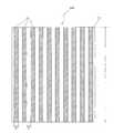
- FIG. 1 shows a plan view of the cut piece.
- a cut piece 100 is formed by printing lines 12 on a polyimide substrate 10 in parallel with each other.
- the length L of the line 12 is 10 mm, and the width W is 400 ⁇ m. Further, the distance D between the lines 12 is also 400 ⁇ m.
- ten lines 12 are formed. However, the number is not limited to this, and an appropriate number can be used.
- the cut piece 100 of FIG. 1 has a non-printed surface fixed to a polyimide film (not shown) with a Kapton tape to form a test piece.
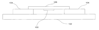
- FIG. 2 shows a schematic cross-sectional view for explaining a method of fixing the test piece.
- the dimensions on the drawing are not correct.
- a quartz plate (length 14 mm ⁇ width 35 mm ⁇ thickness 2 mm) 104 as a spacer is installed 13 mm away from the center position of the quartz plate (length 100 mm ⁇ width 35 mm ⁇ thickness 2 mm) 102.
- the test piece 106 to which the cut piece 100 is fixed has the printing surface of the cut piece 100 facing downward (in the direction of the quartz plate 102), and the cut piece 100 (printed portion) is substantially at the center position between the quartz plates 104 as spacers. In this manner, the quartz plate 104 as a spacer was fixed with Kapton tape.
- the quartz plate 102 on which the test piece 106 was fixed was inserted into an applicator of a microwave heating device (Fuji Radio Engineering Co., Ltd., pulse type heating device FSU-501VP-07). While observing the display temperature of the radiation thermometer, microwaves are irradiated from the vertical direction (from the back of the paper to the front or from the front of the paper) to start heating at an output of 10 W, and the power value gradually increases. After about 8 minutes, the circuit pattern portion printed on the cut piece 100 is heated so that the display temperature of the radiation thermometer is 150 ° C. After maintaining 150 ° C. for 30 seconds (total heating time: 8.5 minutes), heating was stopped. No spark was generated during heating. The radiation thermometer measures the temperature of the line 12 projection on the test piece 106 (opposite to the printing surface). The temperature of the portion is not the temperature of the line 12 itself, but is regarded as a temperature substantially equivalent to that of the line 12.
- a microwave heating device Fluji Radio Engineering Co., Ltd., pulse type heating
- the thickness of the circuit pattern portion was 24 ⁇ m.
- the resistance value between 10 mm in the length direction of the pattern (line 12) of the cut piece 100 was measured using a digital multimeter (TY520 manufactured by Yokogawa Meter & Instruments Co., Ltd.), and as a result, it was 2.0 ⁇ .
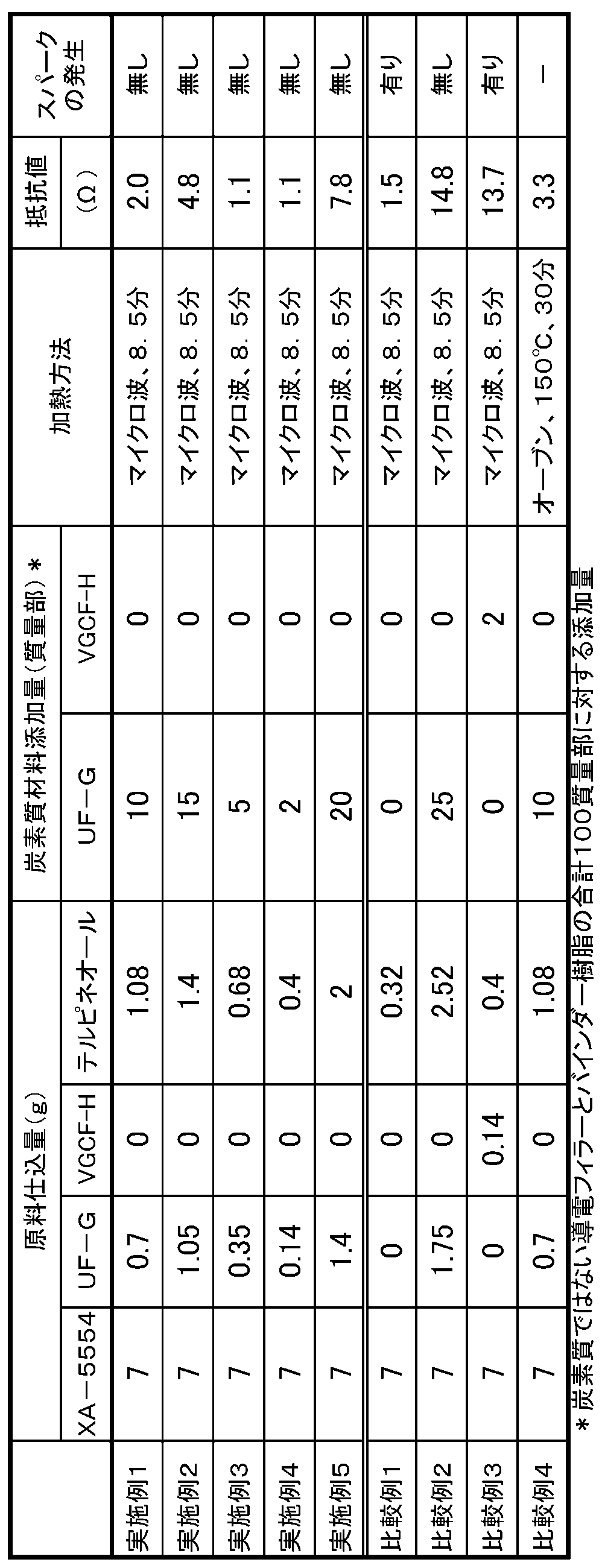
- Examples 2-5, Comparative Examples 1-2 As shown in Table 1, a printing raw material (conductive resin composition) was prepared in the same manner as in Example 1 except that the addition amounts of UF-G10 and terpineol were changed, and a circuit pattern was formed on the polyimide film as in Example 1. After screen printing, microwave heating was performed and the resistance value was measured. The results are summarized in Table 1.
- a raw material conductive resin composition
- a circuit pattern was screen-printed on a polyimide film in the same manner as in Example 4, followed by microwave heating and measurement of the resistance value.
- the thickness of the circuit pattern portion was 25 ⁇ m and the resistance value was 13.7 ⁇ .
- VGCF-H is generally fibrous, and the average length / average diameter of 20 particles arbitrarily selected by SEM observation was determined as the aspect ratio.
- Comparative Example 4 The test piece was heated in the same manner as in Example 1 except that an oven (DASK-TOP TYPE HI-TEMP. CHAMBER ST-110 manufactured by ESPEC) was used instead of the microwave heating apparatus and heated at 150 ° C. for 30 minutes. The resistance value was measured. The thickness of the circuit pattern portion was 28 ⁇ m, and the resistance value was 3.3 ⁇ .
- an oven DASK-TOP TYPE HI-TEMP. CHAMBER ST-110 manufactured by ESPEC
- microwave heating could be performed without generation of sparks. Also, the resistance value of the circuit pattern was sufficiently reduced to less than 10 ⁇ .
- Comparative Example 1 sparks were generated during microwave heating, and a part of the substrate was burnt. This is because the artificial graphite powder (UF-G10) is not added to the conductive resin composition and the microwave energy cannot be absorbed efficiently.
- U-G10 artificial graphite powder
- Comparative Example 2 the resistance value is increased due to the large amount of artificial graphite powder (UF-G10), and the performance as a conductive resin composition is lowered.
- U-G10 artificial graphite powder
- Comparative Example 3 sparks are generated due to the large aspect ratio of the carbonaceous material, and the resistance value is increased and the performance as the conductive resin composition is lowered.
- Comparative Example 4 30 minutes of heating is required to reduce the resistance value of the circuit pattern (3.3 ⁇ ), and productivity is low compared to microwave heating.
Landscapes
- Chemical & Material Sciences (AREA)
- Engineering & Computer Science (AREA)
- Health & Medical Sciences (AREA)
- Chemical Kinetics & Catalysis (AREA)
- Medicinal Chemistry (AREA)
- Polymers & Plastics (AREA)
- Organic Chemistry (AREA)
- Dispersion Chemistry (AREA)
- Microelectronics & Electronic Packaging (AREA)
- Physics & Mathematics (AREA)
- Spectroscopy & Molecular Physics (AREA)
- Manufacturing & Machinery (AREA)
- Materials Engineering (AREA)
- Nanotechnology (AREA)
- General Health & Medical Sciences (AREA)
- Toxicology (AREA)
- Compositions Of Macromolecular Compounds (AREA)
- Conductive Materials (AREA)
- Non-Insulated Conductors (AREA)
- Adhesives Or Adhesive Processes (AREA)
Abstract
Description
XA-5554(藤倉化成株式会社製導電性接着剤)7gに、UF-G10(昭和電工株式会社製、人造黒鉛粉末、平均粒径:4.5μm(カタログ値)、アスペクト比=10)0.7g(100質量部のXA-5554に対して10質量部のUF-G10)、テルピネオール(日本テルペン化学株式会社製Terpineol C) 1.08gを添加し、スパチュラでよく混合し印刷用原料(導電性樹脂組成物)とした。なお、XA-5554の組成は、三菱化学株式会社製エポキシ樹脂jER828(11.8質量部)、日本化薬株式会社製反応性希釈剤GOT[低粘度エポキシ樹脂](7.9質量部)、四国化成工業株式会社製硬化剤2P4MHZ(1.5質量部)、福田金属箔粉工業株式会社製銀粉AgC-GS(78.8質量部)である。UF-G10は概ね扁平状の粒子であり、SEM観察により任意に選択した20個の粒子の平均幅/平均厚みをアスペクト比として求めた。
表1に示すように、UF-G10およびテルピネオールの添加量を変更した以外は実施例1と同様にして印刷用原料(導電性樹脂組成物)を作製し、実施例1同様ポリイミドフィルムに回路パターンをスクリーン印刷後、マイクロ波加熱し、抵抗値の測定を行った。結果をまとめて表1に示した。
表1に示すように、炭素質材料としてUF-G10の代わりにカーボンナノチューブ(昭和電工製、VGCF(登録商標)-H、アスペクト比=40)を使用した以外は実施例4と同様にして印刷用原料(導電性樹脂組成物)を作製し、実施例4同様ポリイミドフィルムに回路パターンをスクリーン印刷後、マイクロ波加熱し、抵抗値の測定を行った。回路パターン部分の厚みは25μmであり、抵抗値は13.7Ωであった。VGCF-Hは概ね繊維状であり、SEM観察により任意に選択した20個の粒子の平均長さ/平均径をアスペクト比として求めた。
比較例4
試験片の加熱をマイクロ波加熱装置の代わりにオーブン(ESPEC社製DASK-TOP TYPE HI-TEMP.CHAMBER ST-110)を使用し、150℃、30分加熱した以外は実施例1と同様にして抵抗値の測定を行った。回路パターン部分の厚みは28μmであり、抵抗値は3.3Ωであった。
Claims (4)
- 炭素質ではない導電フィラーと、硬化性を有する絶縁性のバインダー樹脂と、前記炭素質ではない導電フィラーより体積固有抵抗値が高い炭素質材料とを含み、前記炭素質ではない導電フィラーと硬化性を有する絶縁性のバインダー樹脂の合計100質量部に対してアスペクト比が20以下の炭素質材料を1~20質量部含むことを特徴とするマイクロ波加熱用導電性樹脂組成物。
- 前記炭素質材料が黒鉛粒子である請求項1に記載のマイクロ波加熱用導電性樹脂組成物。
- 前記炭素質ではない導電フィラーが、金、銀、銅、ニッケル、アルミニウム、パラジウムからなる群から選択される少なくとも一種の金属、または前記複数の金属の合金よりなる粒子または繊維、前記金属表面に金、パラジウム、銀のいずれかがめっきされた金属粒子または繊維、樹脂ボールにニッケル、金、パラジウム、銀のいずれかがめっきされた樹脂コアボール、のいずれかである請求項1または請求項2に記載のマイクロ波加熱用導電性樹脂組成物。
- 請求項1から請求項3のいずれか一項に記載のマイクロ波加熱用導電性樹脂組成物を基板にパターン印刷し導電性パターンを形成する工程と、前記導電性パターンにマイクロ波を照射して加熱・硬化する工程と、を有する導電パターンの形成方法。
Priority Applications (5)
| Application Number | Priority Date | Filing Date | Title |
|---|---|---|---|
| JP2015521414A JP6407148B2 (ja) | 2013-06-03 | 2014-05-29 | マイクロ波加熱用導電性樹脂組成物 |
| CN201480031664.2A CN105283513B (zh) | 2013-06-03 | 2014-05-29 | 微波加热用导电性树脂组合物 |
| US14/895,225 US20160133350A1 (en) | 2013-06-03 | 2014-05-29 | Conductive resin composition for microwave heating |
| KR1020187010545A KR102090492B1 (ko) | 2013-06-03 | 2014-05-29 | 마이크로파 가열용 도전성 수지 조성물 |
| KR1020157031891A KR102049322B1 (ko) | 2013-06-03 | 2014-05-29 | 마이크로파 가열용 도전성 수지 조성물 |
Applications Claiming Priority (2)
| Application Number | Priority Date | Filing Date | Title |
|---|---|---|---|
| JP2013-116824 | 2013-06-03 | ||
| JP2013116824 | 2013-06-03 |
Publications (1)
| Publication Number | Publication Date |
|---|---|
| WO2014196444A1 true WO2014196444A1 (ja) | 2014-12-11 |
Family
ID=52008090
Family Applications (1)
| Application Number | Title | Priority Date | Filing Date |
|---|---|---|---|
| PCT/JP2014/064277 Ceased WO2014196444A1 (ja) | 2013-06-03 | 2014-05-29 | マイクロ波加熱用導電性樹脂組成物 |
Country Status (6)
| Country | Link |
|---|---|
| US (1) | US20160133350A1 (ja) |
| JP (1) | JP6407148B2 (ja) |
| KR (2) | KR102090492B1 (ja) |
| CN (1) | CN105283513B (ja) |
| TW (1) | TWI621134B (ja) |
| WO (1) | WO2014196444A1 (ja) |
Cited By (2)
| Publication number | Priority date | Publication date | Assignee | Title |
|---|---|---|---|---|
| JP2018004830A (ja) * | 2016-06-29 | 2018-01-11 | 日本電信電話株式会社 | 高耐熱性光ファイバモジュールおよびその作製方法 |
| JP2022151170A (ja) * | 2021-03-26 | 2022-10-07 | 株式会社カネカ | 熱硬化性樹脂組成物およびそれを用いた硬化成形体の製造方法 |
Families Citing this family (4)
| Publication number | Priority date | Publication date | Assignee | Title |
|---|---|---|---|---|
| CN105522791B (zh) * | 2016-02-03 | 2017-02-22 | 武汉华尚绿能科技股份有限公司 | 高导通夹胶透明玻璃 |
| CN105722332B (zh) * | 2016-03-08 | 2017-03-22 | 上海安费诺永亿通讯电子有限公司 | 一种线路的制作方法 |
| CN109401257B (zh) * | 2018-09-03 | 2021-06-08 | 当阳市益红金属制品有限公司 | 纤维增强复合材料及其制备方法和应用 |
| CN115895550B (zh) * | 2023-02-14 | 2026-03-06 | 江苏澳盛复合材料科技股份有限公司 | 一种环氧树脂粘结剂、制备方法及应用 |
Citations (8)
| Publication number | Priority date | Publication date | Assignee | Title |
|---|---|---|---|---|
| JPS6174205A (ja) * | 1984-09-17 | 1986-04-16 | ダイソー株式会社 | 異方導電性組成物 |
| JPH03285301A (ja) * | 1990-03-31 | 1991-12-16 | Toagosei Chem Ind Co Ltd | 抵抗器用カーボンペースト組成物 |
| JPH06318724A (ja) * | 1993-05-07 | 1994-11-15 | Canon Inc | 電極及び光起電力素子 |
| JPH07205319A (ja) * | 1994-01-24 | 1995-08-08 | Mitsui Toatsu Chem Inc | 加熱方法 |
| JP2010515233A (ja) * | 2007-01-05 | 2010-05-06 | ビーエーエスエフ ソシエタス・ヨーロピア | 導電性表面の形成方法 |
| JP2011521044A (ja) * | 2008-05-13 | 2011-07-21 | エアバス オペレーションズ リミテッド | 熱硬化性エポキシ樹脂、複合材料、複合材料物品の形成方法、モールドおよびモールドの作製方法 |
| WO2013077447A1 (ja) * | 2011-11-24 | 2013-05-30 | 昭和電工株式会社 | 導電パターン形成方法及び光照射またはマイクロ波加熱による導電パターン形成用組成物 |
| WO2014050828A1 (ja) * | 2012-09-25 | 2014-04-03 | 昭和電工株式会社 | マイクロ波加熱装置 |
Family Cites Families (18)
| Publication number | Priority date | Publication date | Assignee | Title |
|---|---|---|---|---|
| GB2152060B (en) * | 1983-12-02 | 1987-05-13 | Osaka Soda Co Ltd | Electrically conductive adhesive composition |
| US5395876A (en) * | 1993-04-19 | 1995-03-07 | Acheson Industries, Inc. | Surface mount conductive adhesives |
| DE19515342A1 (de) | 1995-04-26 | 1996-10-31 | Widia Gmbh | Verfahren, Vorrichtung zur thermischen Behandlung von Stoffen in einem Mikrowellenofen und Verwendung dieses Verfahrens und dieser Vorrichtung |
| US6228288B1 (en) * | 2000-04-27 | 2001-05-08 | Cts Corporation | Electrically conductive compositions and films for position sensors |
| JP2003064314A (ja) | 2001-08-23 | 2003-03-05 | Nippon Paint Co Ltd | 塗料組成物 |
| US20030113531A1 (en) * | 2001-12-19 | 2003-06-19 | Karel Hajmrle | Conductive fillers and conductive polymers made therefrom |
| US20050236182A1 (en) * | 2002-06-04 | 2005-10-27 | Noriki Hayashi | Board for printed wiring, printed wiring board, and method for manufacturing them |
| WO2004059663A1 (en) * | 2002-12-26 | 2004-07-15 | Showa Denko K. K. | Carbonaceous material for forming electrically conductive material and use thereof |
| US7108806B2 (en) * | 2003-02-28 | 2006-09-19 | National Starch And Chemical Investment Holding Corporation | Conductive materials with electrical stability and good impact resistance for use in electronics devices |
| JP4994671B2 (ja) * | 2005-01-21 | 2012-08-08 | 昭和電工株式会社 | 導電性樹脂組成物、その製造方法及び用途 |
| JP4609846B2 (ja) | 2005-03-25 | 2011-01-12 | 古河電気工業株式会社 | 金属焼成体の製造方法及びそれに用いられる金属粒子焼成用材料並びにそれにより得られる配線パターン |
| US20070281136A1 (en) * | 2006-05-31 | 2007-12-06 | Cabot Corporation | Ink jet printed reflective features and processes and inks for making them |
| WO2008010297A1 (fr) * | 2006-07-21 | 2008-01-24 | Nippon Kagaku Yakin Co., Ltd. | Composition pour résine thermodurcissable conduisant la chaleur et procédé pour la produire |
| JP2009177149A (ja) | 2007-12-26 | 2009-08-06 | Konica Minolta Holdings Inc | 金属酸化物半導体とその製造方法および薄膜トランジスタ |
| TWI496168B (zh) * | 2008-07-03 | 2015-08-11 | Henkel IP & Holding GmbH | 觸變型導電組合物 |
| JP2010274383A (ja) | 2009-05-29 | 2010-12-09 | Nisshin Seisakusho:Kk | メタルボンド砥石の製造方法及び製造装置 |
| US20150249167A1 (en) * | 2012-10-15 | 2015-09-03 | Dow Global Technologies Llc | Conductive composition |
| US9716299B2 (en) * | 2012-10-25 | 2017-07-25 | The Regents Of The University Of California | Graphene based thermal interface materials and methods of manufacturing the same |
-
2014
- 2014-05-29 KR KR1020187010545A patent/KR102090492B1/ko active Active
- 2014-05-29 CN CN201480031664.2A patent/CN105283513B/zh active Active
- 2014-05-29 KR KR1020157031891A patent/KR102049322B1/ko active Active
- 2014-05-29 US US14/895,225 patent/US20160133350A1/en not_active Abandoned
- 2014-05-29 JP JP2015521414A patent/JP6407148B2/ja active Active
- 2014-05-29 WO PCT/JP2014/064277 patent/WO2014196444A1/ja not_active Ceased
- 2014-06-03 TW TW103119214A patent/TWI621134B/zh active
Patent Citations (8)
| Publication number | Priority date | Publication date | Assignee | Title |
|---|---|---|---|---|
| JPS6174205A (ja) * | 1984-09-17 | 1986-04-16 | ダイソー株式会社 | 異方導電性組成物 |
| JPH03285301A (ja) * | 1990-03-31 | 1991-12-16 | Toagosei Chem Ind Co Ltd | 抵抗器用カーボンペースト組成物 |
| JPH06318724A (ja) * | 1993-05-07 | 1994-11-15 | Canon Inc | 電極及び光起電力素子 |
| JPH07205319A (ja) * | 1994-01-24 | 1995-08-08 | Mitsui Toatsu Chem Inc | 加熱方法 |
| JP2010515233A (ja) * | 2007-01-05 | 2010-05-06 | ビーエーエスエフ ソシエタス・ヨーロピア | 導電性表面の形成方法 |
| JP2011521044A (ja) * | 2008-05-13 | 2011-07-21 | エアバス オペレーションズ リミテッド | 熱硬化性エポキシ樹脂、複合材料、複合材料物品の形成方法、モールドおよびモールドの作製方法 |
| WO2013077447A1 (ja) * | 2011-11-24 | 2013-05-30 | 昭和電工株式会社 | 導電パターン形成方法及び光照射またはマイクロ波加熱による導電パターン形成用組成物 |
| WO2014050828A1 (ja) * | 2012-09-25 | 2014-04-03 | 昭和電工株式会社 | マイクロ波加熱装置 |
Cited By (3)
| Publication number | Priority date | Publication date | Assignee | Title |
|---|---|---|---|---|
| JP2018004830A (ja) * | 2016-06-29 | 2018-01-11 | 日本電信電話株式会社 | 高耐熱性光ファイバモジュールおよびその作製方法 |
| JP2022151170A (ja) * | 2021-03-26 | 2022-10-07 | 株式会社カネカ | 熱硬化性樹脂組成物およびそれを用いた硬化成形体の製造方法 |
| JP7608235B2 (ja) | 2021-03-26 | 2025-01-06 | 株式会社カネカ | 熱硬化性樹脂組成物およびそれを用いた硬化成形体の製造方法 |
Also Published As
| Publication number | Publication date |
|---|---|
| CN105283513A (zh) | 2016-01-27 |
| TWI621134B (zh) | 2018-04-11 |
| US20160133350A1 (en) | 2016-05-12 |
| TW201511039A (zh) | 2015-03-16 |
| JP6407148B2 (ja) | 2018-10-17 |
| JPWO2014196444A1 (ja) | 2017-02-23 |
| KR102049322B1 (ko) | 2019-11-27 |
| KR102090492B1 (ko) | 2020-04-24 |
| KR20180040738A (ko) | 2018-04-20 |
| CN105283513B (zh) | 2018-05-01 |
| KR20150140762A (ko) | 2015-12-16 |
Similar Documents
| Publication | Publication Date | Title |
|---|---|---|
| JP6407148B2 (ja) | マイクロ波加熱用導電性樹脂組成物 | |
| JP4363340B2 (ja) | 導電性銀ペースト及びそれを用いた電磁波シールド部材 | |
| KR101777691B1 (ko) | 그래핀 산화물을 포함하는 발열 조성물 및 그를 이용한 발열체 | |
| KR101143296B1 (ko) | 그라비아 직접 인쇄방식에 적용 가능한 저온 소성용 도전성 페이스트 | |
| JP4936142B2 (ja) | 導電性ペースト組成物及び電子回路並びに電子部品 | |
| KR20100066780A (ko) | 전도성 페이스트와 이를 이용한 전도성 기판 | |
| KR20180059490A (ko) | 도전성 페이스트 및 도전막 | |
| JPWO2013161966A1 (ja) | 導電性組成物 | |
| KR102166230B1 (ko) | 전도성 필러 및 그의 제조 방법, 및 전도성 페이스트 및 그의 제조 방법 | |
| JP2010109334A (ja) | 導電性インク組成物及び該組成物を用いて形成された太陽電池モジュール | |
| WO2012133627A1 (ja) | 銀コート銅粉及びその製造法、該銀コート銅粉を含有する導電性ペースト、導電性接着剤、導電性膜、及び電気回路 | |
| KR20150064054A (ko) | 은 하이브리드 구리분과 그의 제조법, 상기 은 하이브리드 구리분을 함유하는 도전성 페이스트, 도전성 접착제, 도전성 막 및 전기 회로 | |
| JP5184584B2 (ja) | 金属配線パターンの形成方法、金属配線パターン、金属配線基板、および金属配線パターン形成用の金属粒子と基板 | |
| KR101468975B1 (ko) | 저차원 소재 고전도성 전도막 | |
| TWI481644B (zh) | 聚苯胺複合材料及其製造方法 | |
| JP6562196B2 (ja) | 銅微粒子焼結体と導電性基板の製造方法 | |
| JP2014089818A (ja) | 熱硬化型導電性ペースト | |
| JP5353163B2 (ja) | 導電性インク組成物及び該組成物を用いて集電極が形成された太陽電池セル | |
| JPWO2019004331A1 (ja) | 導電性ペースト | |
| KR20180058903A (ko) | 절연 잉크 조성물 및 그를 이용하여 절연막이 형성된 기판 | |
| JP2010235738A (ja) | 導電性インキ | |
| JP2022113635A (ja) | 電磁波シールド用組成物、電磁波シールドシート付基体の製造方法、電磁波シールドシート及びプリント配線基板 | |
| JP5692295B2 (ja) | 太陽電池セルの集電極の形成方法及び該太陽電池セルを備えた太陽電池モジュール | |
| JP6574553B2 (ja) | 導電パターン形成用組成物および導電パターン形成方法 | |
| JP2010232247A (ja) | 電磁波抑制材料 |
Legal Events
| Date | Code | Title | Description |
|---|---|---|---|
| WWE | Wipo information: entry into national phase |
Ref document number: 201480031664.2 Country of ref document: CN |
|
| 121 | Ep: the epo has been informed by wipo that ep was designated in this application |
Ref document number: 14806995 Country of ref document: EP Kind code of ref document: A1 |
|
| ENP | Entry into the national phase |
Ref document number: 20157031891 Country of ref document: KR Kind code of ref document: A |
|
| ENP | Entry into the national phase |
Ref document number: 2015521414 Country of ref document: JP Kind code of ref document: A |
|
| WWE | Wipo information: entry into national phase |
Ref document number: 14895225 Country of ref document: US |
|
| NENP | Non-entry into the national phase |
Ref country code: DE |
|
| 122 | Ep: pct application non-entry in european phase |
Ref document number: 14806995 Country of ref document: EP Kind code of ref document: A1 |