WO2014175343A1 - 半導体装置および半導体装置の製造方法 - Google Patents
半導体装置および半導体装置の製造方法 Download PDFInfo
- Publication number
- WO2014175343A1 WO2014175343A1 PCT/JP2014/061457 JP2014061457W WO2014175343A1 WO 2014175343 A1 WO2014175343 A1 WO 2014175343A1 JP 2014061457 W JP2014061457 W JP 2014061457W WO 2014175343 A1 WO2014175343 A1 WO 2014175343A1
- Authority
- WO
- WIPO (PCT)
- Prior art keywords
- wire
- bonding
- semiconductor device
- electrode
- metal film
- Prior art date
- Legal status (The legal status is an assumption and is not a legal conclusion. Google has not performed a legal analysis and makes no representation as to the accuracy of the status listed.)
- Ceased
Links
Images







Classifications
-
- H—ELECTRICITY
- H10—SEMICONDUCTOR DEVICES; ELECTRIC SOLID-STATE DEVICES NOT OTHERWISE PROVIDED FOR
- H10W—GENERIC PACKAGES, INTERCONNECTIONS, CONNECTORS OR OTHER CONSTRUCTIONAL DETAILS OF DEVICES COVERED BY CLASS H10
- H10W72/00—Interconnections or connectors in packages
- H10W72/01—Manufacture or treatment
- H10W72/019—Manufacture or treatment of bond pads
-
- H—ELECTRICITY
- H10—SEMICONDUCTOR DEVICES; ELECTRIC SOLID-STATE DEVICES NOT OTHERWISE PROVIDED FOR
- H10W—GENERIC PACKAGES, INTERCONNECTIONS, CONNECTORS OR OTHER CONSTRUCTIONAL DETAILS OF DEVICES COVERED BY CLASS H10
- H10W72/00—Interconnections or connectors in packages
- H10W72/01—Manufacture or treatment
- H10W72/015—Manufacture or treatment of bond wires
-
- H—ELECTRICITY
- H10—SEMICONDUCTOR DEVICES; ELECTRIC SOLID-STATE DEVICES NOT OTHERWISE PROVIDED FOR
- H10W—GENERIC PACKAGES, INTERCONNECTIONS, CONNECTORS OR OTHER CONSTRUCTIONAL DETAILS OF DEVICES COVERED BY CLASS H10
- H10W72/00—Interconnections or connectors in packages
- H10W72/071—Connecting or disconnecting
- H10W72/075—Connecting or disconnecting of bond wires
-
- H—ELECTRICITY
- H10—SEMICONDUCTOR DEVICES; ELECTRIC SOLID-STATE DEVICES NOT OTHERWISE PROVIDED FOR
- H10W—GENERIC PACKAGES, INTERCONNECTIONS, CONNECTORS OR OTHER CONSTRUCTIONAL DETAILS OF DEVICES COVERED BY CLASS H10
- H10W72/00—Interconnections or connectors in packages
- H10W72/071—Connecting or disconnecting
- H10W72/075—Connecting or disconnecting of bond wires
- H10W72/07531—Techniques
- H10W72/07532—Compression bonding, e.g. thermocompression bonding
-
- H—ELECTRICITY
- H10—SEMICONDUCTOR DEVICES; ELECTRIC SOLID-STATE DEVICES NOT OTHERWISE PROVIDED FOR
- H10W—GENERIC PACKAGES, INTERCONNECTIONS, CONNECTORS OR OTHER CONSTRUCTIONAL DETAILS OF DEVICES COVERED BY CLASS H10
- H10W72/00—Interconnections or connectors in packages
- H10W72/071—Connecting or disconnecting
- H10W72/075—Connecting or disconnecting of bond wires
- H10W72/07531—Techniques
- H10W72/07532—Compression bonding, e.g. thermocompression bonding
- H10W72/07533—Ultrasonic bonding, e.g. thermosonic bonding
-
- H—ELECTRICITY
- H10—SEMICONDUCTOR DEVICES; ELECTRIC SOLID-STATE DEVICES NOT OTHERWISE PROVIDED FOR
- H10W—GENERIC PACKAGES, INTERCONNECTIONS, CONNECTORS OR OTHER CONSTRUCTIONAL DETAILS OF DEVICES COVERED BY CLASS H10
- H10W72/00—Interconnections or connectors in packages
- H10W72/071—Connecting or disconnecting
- H10W72/075—Connecting or disconnecting of bond wires
- H10W72/07551—Connecting or disconnecting of bond wires characterised by changes in properties of the bond wires during the connecting
- H10W72/07555—Connecting or disconnecting of bond wires characterised by changes in properties of the bond wires during the connecting changes in materials
-
- H—ELECTRICITY
- H10—SEMICONDUCTOR DEVICES; ELECTRIC SOLID-STATE DEVICES NOT OTHERWISE PROVIDED FOR
- H10W—GENERIC PACKAGES, INTERCONNECTIONS, CONNECTORS OR OTHER CONSTRUCTIONAL DETAILS OF DEVICES COVERED BY CLASS H10
- H10W72/00—Interconnections or connectors in packages
- H10W72/30—Die-attach connectors
- H10W72/351—Materials of die-attach connectors
- H10W72/352—Materials of die-attach connectors comprising metals or metalloids, e.g. solders
-
- H—ELECTRICITY
- H10—SEMICONDUCTOR DEVICES; ELECTRIC SOLID-STATE DEVICES NOT OTHERWISE PROVIDED FOR
- H10W—GENERIC PACKAGES, INTERCONNECTIONS, CONNECTORS OR OTHER CONSTRUCTIONAL DETAILS OF DEVICES COVERED BY CLASS H10
- H10W72/00—Interconnections or connectors in packages
- H10W72/50—Bond wires
- H10W72/551—Materials of bond wires
-
- H—ELECTRICITY
- H10—SEMICONDUCTOR DEVICES; ELECTRIC SOLID-STATE DEVICES NOT OTHERWISE PROVIDED FOR
- H10W—GENERIC PACKAGES, INTERCONNECTIONS, CONNECTORS OR OTHER CONSTRUCTIONAL DETAILS OF DEVICES COVERED BY CLASS H10
- H10W72/00—Interconnections or connectors in packages
- H10W72/50—Bond wires
- H10W72/551—Materials of bond wires
- H10W72/552—Materials of bond wires comprising metals or metalloids, e.g. silver
- H10W72/5524—Materials of bond wires comprising metals or metalloids, e.g. silver comprising aluminium [Al]
-
- H—ELECTRICITY
- H10—SEMICONDUCTOR DEVICES; ELECTRIC SOLID-STATE DEVICES NOT OTHERWISE PROVIDED FOR
- H10W—GENERIC PACKAGES, INTERCONNECTIONS, CONNECTORS OR OTHER CONSTRUCTIONAL DETAILS OF DEVICES COVERED BY CLASS H10
- H10W72/00—Interconnections or connectors in packages
- H10W72/50—Bond wires
- H10W72/551—Materials of bond wires
- H10W72/552—Materials of bond wires comprising metals or metalloids, e.g. silver
- H10W72/5525—Materials of bond wires comprising metals or metalloids, e.g. silver comprising copper [Cu]
-
- H—ELECTRICITY
- H10—SEMICONDUCTOR DEVICES; ELECTRIC SOLID-STATE DEVICES NOT OTHERWISE PROVIDED FOR
- H10W—GENERIC PACKAGES, INTERCONNECTIONS, CONNECTORS OR OTHER CONSTRUCTIONAL DETAILS OF DEVICES COVERED BY CLASS H10
- H10W72/00—Interconnections or connectors in packages
- H10W72/50—Bond wires
- H10W72/59—Bond pads specially adapted therefor
-
- H—ELECTRICITY
- H10—SEMICONDUCTOR DEVICES; ELECTRIC SOLID-STATE DEVICES NOT OTHERWISE PROVIDED FOR
- H10W—GENERIC PACKAGES, INTERCONNECTIONS, CONNECTORS OR OTHER CONSTRUCTIONAL DETAILS OF DEVICES COVERED BY CLASS H10
- H10W72/00—Interconnections or connectors in packages
- H10W72/851—Dispositions of multiple connectors or interconnections
- H10W72/874—On different surfaces
- H10W72/884—Die-attach connectors and bond wires
-
- H—ELECTRICITY
- H10—SEMICONDUCTOR DEVICES; ELECTRIC SOLID-STATE DEVICES NOT OTHERWISE PROVIDED FOR
- H10W—GENERIC PACKAGES, INTERCONNECTIONS, CONNECTORS OR OTHER CONSTRUCTIONAL DETAILS OF DEVICES COVERED BY CLASS H10
- H10W72/00—Interconnections or connectors in packages
- H10W72/90—Bond pads, in general
- H10W72/921—Structures or relative sizes of bond pads
-
- H—ELECTRICITY
- H10—SEMICONDUCTOR DEVICES; ELECTRIC SOLID-STATE DEVICES NOT OTHERWISE PROVIDED FOR
- H10W—GENERIC PACKAGES, INTERCONNECTIONS, CONNECTORS OR OTHER CONSTRUCTIONAL DETAILS OF DEVICES COVERED BY CLASS H10
- H10W72/00—Interconnections or connectors in packages
- H10W72/90—Bond pads, in general
- H10W72/921—Structures or relative sizes of bond pads
- H10W72/923—Bond pads having multiple stacked layers
-
- H—ELECTRICITY
- H10—SEMICONDUCTOR DEVICES; ELECTRIC SOLID-STATE DEVICES NOT OTHERWISE PROVIDED FOR
- H10W—GENERIC PACKAGES, INTERCONNECTIONS, CONNECTORS OR OTHER CONSTRUCTIONAL DETAILS OF DEVICES COVERED BY CLASS H10
- H10W72/00—Interconnections or connectors in packages
- H10W72/90—Bond pads, in general
- H10W72/951—Materials of bond pads
- H10W72/952—Materials of bond pads comprising metals or metalloids, e.g. PbSn, Ag or Cu
-
- H—ELECTRICITY
- H10—SEMICONDUCTOR DEVICES; ELECTRIC SOLID-STATE DEVICES NOT OTHERWISE PROVIDED FOR
- H10W—GENERIC PACKAGES, INTERCONNECTIONS, CONNECTORS OR OTHER CONSTRUCTIONAL DETAILS OF DEVICES COVERED BY CLASS H10
- H10W90/00—Package configurations
- H10W90/701—Package configurations characterised by the relative positions of pads or connectors relative to package parts
- H10W90/731—Package configurations characterised by the relative positions of pads or connectors relative to package parts of die-attach connectors
- H10W90/734—Package configurations characterised by the relative positions of pads or connectors relative to package parts of die-attach connectors between a chip and a stacked insulating package substrate, interposer or RDL
-
- H—ELECTRICITY
- H10—SEMICONDUCTOR DEVICES; ELECTRIC SOLID-STATE DEVICES NOT OTHERWISE PROVIDED FOR
- H10W—GENERIC PACKAGES, INTERCONNECTIONS, CONNECTORS OR OTHER CONSTRUCTIONAL DETAILS OF DEVICES COVERED BY CLASS H10
- H10W90/00—Package configurations
- H10W90/701—Package configurations characterised by the relative positions of pads or connectors relative to package parts
- H10W90/751—Package configurations characterised by the relative positions of pads or connectors relative to package parts of bond wires
- H10W90/754—Package configurations characterised by the relative positions of pads or connectors relative to package parts of bond wires between a chip and a stacked insulating package substrate, interposer or RDL
Definitions
- the present invention relates to a semiconductor device and a method for manufacturing the semiconductor device.
- the front electrode and circuit layer of a semiconductor element are electrically connected by wire bonding such as aluminum (Al) wire.
- wire bonding such as aluminum (Al) wire.
- the front surface electrode is, for example, an aluminum-silicon (Si) electrode or an Al-Si-copper (Cu) electrode
- the circuit layer is made of a conductor such as Cu.
- wire bonding of Cu wires has been studied in place of Al wires. A structure of a conventional semiconductor device having a module structure will be described.
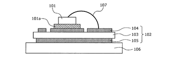
- FIG. 10 is a sectional view showing the structure of a conventional semiconductor device having a module structure.
- FIG. 11 is a cross-sectional view schematically showing the structure of the semiconductor element of FIG.
- a conventional semiconductor device having a module structure includes a semiconductor element 101, an insulating substrate 102 such as a ceramic insulating substrate (DCB (Direct Copper Bonding) substrate), a Cu base 106, and an Al wire 107. ing.
- the insulating substrate 102 is provided with a circuit layer 104 made of Cu on the front surface side of the insulating layer 103 and a back copper foil 105 on the back surface side.
- the semiconductor element 101 has a front electrode 112 on the front surface of the semiconductor substrate 111 and a back electrode 113 on the back surface.
- the back electrode 113 of the semiconductor element 101 is bonded to the circuit layer 104 via the solder bonding layer 101a.
- the front surface electrode 112 of the semiconductor element 101 is electrically connected to the circuit layer 104 by wire bonding such as an Al wire 107.
- the Al wire 107 is joined using ultrasonic vibration, and the connection failure is reduced by optimizing conditions such as heat, ultrasonic vibration, and applied pressure with respect to the diameter (diameter) of the Al wire 107. A good bond is formed without causing it.
- the front surface of the Cu base 106 is bonded to the back copper foil 105 via a solder bonding layer (not shown).
- the recrystallization temperature is set to 150 ° C. or more so as to have an average crystal grain size of 50 ⁇ m or more in connection between the element and the external electrode and not to cause recrystallization when energized.
- An apparatus composed of an aluminum wire containing 0.02 wt% to 1 wt% of Fe for increasing has been proposed (see, for example, Patent Document 1 below).
- the film is formed on the top surface of the surface electrode.
- a device including a metal protective film, and a wire wiring electrically bonded to the surface electrode via the metal protective film by thermocompression bonding or ultrasonic vibration (see, for example, Patent Document 4 below). ).
- Factors that determine the power cycle tolerance are the maximum value Tjmax of the junction temperature of the semiconductor element and the temperature change ⁇ Tj of the junction temperature of the semiconductor element caused by the intermittent flow of current.
- the constituent members of the semiconductor device have different linear expansion coefficients, and each constituent member is subjected to a stress corresponding to the difference in the linear expansion coefficients.
- Tjmax of the junction temperature of the semiconductor element increases, the stress corresponding to the difference in the linear expansion coefficient of each constituent member increases, which may lead to element destruction. For this reason, it is necessary to improve the power cycle tolerance in high temperature operation, and to achieve high temperature operation and high reliability at the same time.
- the crystal grains near the bonding interface of the Al wire become fine particles due to wire bonding, and the bonding strength of the Al wire is improved.
- the high-temperature operation for example, about 175 ° C.
- the vicinity of the bonding interface of the Al wire and the crystal grains of the front electrode are coarsened and softened.
- cracks are likely to occur in the vicinity of the bonding interface between the Al wire and the front electrode.
- a crack was generated in the Al wire, and this crack progressed to the inside of the wire with an increase in the number of repeated power cycles. It was found that the device was destroyed.
- An object of the present invention is to provide a semiconductor device and a method for manufacturing the semiconductor device that can improve power cycle tolerance in large current conduction and high-temperature operation in order to eliminate the above-described problems caused by the prior art.
- a semiconductor device has the following characteristics in a semiconductor device in which electrodes of a semiconductor element and wires are electrically connected by wire bonding.
- a metal film having a hardness higher than that of the wire is provided on the surface of the electrode.
- the wire is bonded to the metal film by wire bonding.
- the recrystallization temperature of the joint interface with the said metal film of the said wire is 175 degreeC or more.
- the crystal grain size of the bonding interface of the wire is 15 ⁇ m or less, and a portion apart from the bonding interface of the wire is a crystal having a particle size of greater than 15 ⁇ m. It is characterized by containing grains.
- the hardness of the wire is higher than the hardness of the electrode.
- the semiconductor device according to the present invention is characterized in that, in the above-described invention, the metal film is a nickel plating film.
- the semiconductor device according to the present invention is characterized in that, in the above-described invention, the thickness of the nickel plating film is 3 ⁇ m to 7 ⁇ m.
- the semiconductor device according to the present invention is characterized in that, in the above-described invention, the metal film is a copper plating film.
- the semiconductor device according to the present invention is characterized in that, in the above-described invention, the thickness of the copper plating film is 4.5 ⁇ m to 10.5 ⁇ m.
- a semiconductor device manufacturing method includes a semiconductor device manufacturing method in which an electrode of a semiconductor element and a wire are electrically connected. It has the characteristics of. First, a step of providing a metal film having a higher hardness than the wire on the surface of the electrode is performed. Next, the step of bonding the wire to the metal film is performed by setting the crystal grain size of the bonding interface between the wire and the metal film to 15 ⁇ m or less by ultrasonic vibration of wire bonding.
- the recrystallization temperature of the wire higher than the recrystallization temperature of the conventional aluminum wire, it is possible to suppress the occurrence of cracks in the wire even under use conditions at a higher temperature than in the past. . Thereby, the period until a crack arises in a wire can be made longer than before.
- the electrode can be strengthened by providing a metal film having a hardness higher than that of the wire on the surface of the electrode of the semiconductor element (semiconductor chip), so that the electrode is prevented from being cracked. can do.
- the metal film functions as a barrier. Therefore, even when a crack occurs in the wire, the crack can be prevented from progressing to the electrode. .
- FIG. 1 is a cross-sectional view illustrating the structure of the semiconductor device according to the embodiment.
- FIG. 2 is a cross-sectional view schematically showing the structure of the semiconductor element of FIG.
- FIG. 3 is a cross-sectional view schematically showing a state of crystal grains in the vicinity of the wire bonding interface of the semiconductor device according to the embodiment.
- FIG. 4 is a cross-sectional view schematically showing the state of crystal grains in the vicinity of the wire bonding interface of the semiconductor device of the reference example.
- FIG. 5 is a cross-sectional view schematically showing the state of crystal grains in the vicinity of the wire bonding interface of a conventional semiconductor device.
- FIG. 6 is a characteristic diagram illustrating the bonding strength of the wires of the semiconductor device according to the embodiment.
- FIG. 7 is a characteristic diagram showing the bonding strength of wires of a conventional semiconductor device.
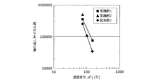
- FIG. 8 is a characteristic diagram showing the power cycle capability of the semiconductor device according to the embodiment.
- FIG. 9 is a cross-sectional view schematically showing a state in the vicinity of the bonding interface of the wire after the wire bonding of the semiconductor device according to the embodiment.
- FIG. 10 is a cross-sectional view showing the structure of a conventional semiconductor device having a module structure.
- FIG. 11 is a cross-sectional view schematically showing the structure of the semiconductor element of FIG.
- FIG. 12 is a characteristic diagram illustrating the bonding strength of the wires of the semiconductor device according to the embodiment.
- FIG. 13 is a characteristic diagram illustrating the bonding strength of another example of the semiconductor device according to the embodiment.
- FIG. 14 is a characteristic diagram showing the bonding strength of another example of a conventional semiconductor device.
- FIG. 1 is a cross-sectional view illustrating the structure of the semiconductor device according to the embodiment.
- FIG. 2 is a cross-sectional view schematically showing the structure of the semiconductor element of FIG.
- the semiconductor device according to the embodiment includes a semiconductor element (semiconductor chip) 1, an insulating substrate 2 such as a ceramics insulating substrate (DCB substrate), a copper (Cu) base 6, and wires.
- 7 is a module-structured semiconductor device.
- the insulating substrate 2 is provided with a circuit layer 4 made of, for example, Cu on the front surface side of the insulating layer 3 and a back copper foil 5 on the back surface side.
- the semiconductor element 1 has a front electrode 12 on the front surface of a semiconductor substrate (for example, a silicon (Si) substrate, a silicon carbide (SiC) substrate, a gallium nitride (GaN) substrate, etc.) 11, and the rear surface.
- a back electrode 13 is provided.
- the back electrode 13 of the semiconductor element 1 is bonded to the circuit layer 4 via the solder bonding layer 1a.
- the front surface of the Cu base 6 is bonded to the back copper foil 5 via a solder bonding layer (not shown).
- a resin case provided with external terminals is bonded to the periphery of the Cu base 6.
- the semiconductor device is used with the back surface of the Cu base 6 fixed to a cooling body via a thermal compound.
- the front surface electrode (hereinafter simply referred to as front surface electrode) 12 of the semiconductor element 1 is, for example, an aluminum (Al) -silicon (Si) electrode.
- the crystal grain size of the front electrode 12 may be, for example, 1 ⁇ m to 5 ⁇ m.
- a front surface metal film 14 such as a nickel (Ni) film or a copper (Cu) film is formed on the surface of the front surface electrode 12 by electroless plating, electrolytic plating, sputtering, vapor deposition, or the like. Yes.
- the hardness of the front surface metal film 14 is higher than the hardness of the front surface electrode 12 and the wire 7.
- the front metal film 14 has a function of improving the strength of the front electrode 12 and preventing the front electrode 12 from cracking.
- the hardness of the front metal film 14 is preferably Hv100 to Hv900, for example.
- the thickness of the front metal film 14 is preferably 3 ⁇ m to 30 ⁇ m, for example.
- the thickness of the front surface metal film 14 is 3 ⁇ m to 7 ⁇ m, preferably 3 ⁇ m to 5 ⁇ m.
- the reason for setting the film thickness to 3 ⁇ m or more is that when a Ni plating film is formed as the front metal film 14, if the plating film thickness is less than 3 ⁇ m, frictional heat generated when wire 7 is wire bonded, This is because the plating film is destroyed by the solid phase flow.
- the breaking strength of the front metal film 14 can be increased, but in consideration of throughput and economy, it is 30 ⁇ m or less, preferably 5 ⁇ m or less. It is good.
- the thickness of the front surface metal film 14 is 4.5 ⁇ m to 10.5 ⁇ m, preferably 4.5 ⁇ m to 7.5 ⁇ m. Since the hardness of the Cu plating film is in the range of Hv100 to Hv300, the fracture strength equivalent to that of the Ni plating film can be obtained by making the film thickness about 1.5 times that of the Ni plating film. Also, when the front metal film 14 is formed by sputtering or vapor deposition, the above-mentioned hardness and film thickness are preferably set for the same reason.
- the front surface electrode 12 and the circuit layer 4 are electrically connected via a wire 7.
- one end of the wire 7 is bonded to the front surface metal film 14 on the surface of the front electrode 12 by wire bonding using heat, ultrasonic vibration and pressure (bonding load). Is connected to the circuit layer 4 at the other end.
- the bonding load for bonding the wire 7 and the member to be bonded is, for example, a wire bonder BJ935 (ultrasonic frequency 60 kHz) manufactured by H & K (Hess & Knipps GmbH).
- the wire bonding ultrasonic output is 11 V or more, for example, 800 gf to 1400 gf, and when the wire bonding ultrasonic output is 13 V or more, 1000 gf to 1400 gf.
- the wire 7 is made of, for example, iron (Fe) of 0.2 mass% to 2.0 mass% and the balance of aluminum (Al) having a purity of 99.99% or more. It is a high heat resistant aluminum wire.
- the crystal grain size of the wire 7 is controlled to be smaller than the crystal grain size of the conventional aluminum wire by containing a predetermined amount of Fe.
- the recrystallization temperature of the wire 7 is increased to at least 175 ° C. or more, and the hardness of the wire 7 is higher than the hardness of the front electrode 12.
- the hardness of the wire 7 is higher than the hardness Hv20 of the AlSi electrode which is the front electrode 12, for example, immediately after the wire bonding.
- the recrystallization temperature of the wire 7 By setting the recrystallization temperature of the wire 7 within the above range, the heat history due to the manufacturing process after wire bonding and the high temperature operation (for example, about 175 ° C.) due to energization / heating of the semiconductor element 1 (hereinafter, the heat history and energization / heating are reduced Since the wire 7 is not recrystallized, the crystal grains of the wire 7 can be prevented from becoming coarse. As a result, during energization heat generation, the crystal grains of the wire 7 are not substantially changed, and the hardness of the wire 7 is maintained in a state immediately after the wire bonding. Therefore, the wire 7 is not easily softened by the power cycle, and the wire 7 is less likely to be cracked than before.
- the crystal grain size of the wire 7 before wire bonding is preferably the maximum, for example, in the range of 1 ⁇ m to 20 ⁇ m.
- the crystal grains in the vicinity of the bonding interface between the wire 7 and the member to be bonded (hereinafter referred to as the bonding interface of the wire 7) can be made into fine particles by controlling the conditions during wire bonding.
- the crystal grain size of the wire 7 extends from the bonding interface of the wire 7 to the axial direction of the wire 7 up to a portion where cracks are likely to occur due to heat history in the manufacturing process after wire bonding or high-temperature operation heat due to energization heat generation of the semiconductor element. It is preferably finely grained by wire bonding.
- the crystal grain size of the wire 7 immediately after the wire bonding is, for example, in the range of 1 ⁇ m to 15 ⁇ m at the maximum (average is 3 ⁇ m or less) in the crystal grains near the bonding interface with the bonded member.
- the crystal grain size before wire bonding is maintained in a portion away from the bonding interface (other than the vicinity of the bonding interface of the wire 7).
- the crystal grain size is evaluated by an electron beam backscatter diffraction method (EBSD: Electron Backscatter Diffraction).
- EBSD Electron Backscatter Diffraction
- the wire diameter of the wire 7 may be, for example, 100 ⁇ m to 500 ⁇ m.
- the wire diameter of the wire 7 is thickened to about 500 ⁇ m, for example. The reason is that the wire heating temperature during energization can be reduced by thickening.
- Ni is plated as the front surface metal film 14 on the surface of the AlSi electrode that is the front surface electrode 12 by using an electroless nickel plating method.
- a zincate treatment is generally performed as a pretreatment for the electroless plating treatment to improve the adhesion of the nickel plating film to the AlSi electrode.
- the surface of the front electrode 12 is degreased to remove oily dirt and foreign matter adhering to the surface and clean it.
- the wettability of the front electrode 12 such as an etching solution in the subsequent process is improved.
- an etching process is performed using an acid solution.
- acid cleaning is performed using a nitric acid (HNO 3 ) solution to remove deposits (smut) generated by the etching treatment.
- a first zincate treatment is performed to replace Al on the surface of the front electrode 12 with zinc (Zn), and a Zn film having a desired crystal grain size is generated on the surface of the front electrode 12. .
- the Zn film formed on the surface of the front electrode 12 is removed using a nitric acid solution.
- a Zn film is formed again on the surface of the front electrode 12 by performing a second zincate process.
- an electroless Ni plating process is performed to replace the Zn film with Ni, and Ni is continuously deposited on the surface of the front electrode 12 to form a Ni plating film.
- a Ni plating film is formed as the front metal film 14 on the surface of the front electrode 12.
- a Ni plating film may be formed as a protective film for the front electrode 12 by a palladium process.
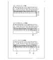
- FIG. 3 is a cross-sectional view schematically showing a state of crystal grains in the vicinity of the wire bonding interface of the semiconductor device according to the embodiment.
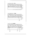
- FIG. 4 is a cross-sectional view schematically showing the state of crystal grains in the vicinity of the wire bonding interface of the semiconductor device of the reference example.
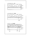
- FIG. 5 is a cross-sectional view schematically showing the state of crystal grains in the vicinity of the wire bonding interface of a conventional semiconductor device. 3 to 5, (a) shows a state before wire bonding, (b) shows a state immediately after wire bonding, and (c) shows a state after a power cycle test.
- the semiconductor device according to the above-described embodiment hereinafter referred to as an example
- the state of the crystal grains in the vicinity of the bonding interface 20 of the wire 7 observed with a microscope after the power cycle test is schematically shown in FIG.
- the wire diameter of the wire 7 was set to 400 ⁇ m, and the crystal grain size of the wire 7 before wire bonding was set within a range of 1 ⁇ m to 20 ⁇ m.
- the crystal grain size in the vicinity of the bonding interface 20 of the wire 7 after wire bonding is in the range of 1 ⁇ m to 15 ⁇ m, and the crystal grain size of the part away from the bonding interface 20 of the wire 7 after wire bonding indicates the state before the wire bonding. It was maintained within a range of 1 ⁇ m to 20 ⁇ m.
- the hardness of the wire 7 after wire bonding is Hv25 to Hv40.
- a 0.3 ⁇ m thick Ni plating film (Example 1) and a 5 ⁇ m thick Ni plating film (Example 2) were formed.
- the hardness of the Ni plating film is Hv900.
- An AlSi electrode was formed as the front electrode 12, and the crystal grain size was in the range of 1 ⁇ m to 5 ⁇ m.
- a semiconductor device (hereinafter referred to as a reference example) in which the front surface metal film 14 is not provided, that is, the wire 37 is bonded to the front surface electrode 32 of the front surface of the semiconductor substrate 31 is implemented.
- the result of conducting the same power cycle test with the same number of repeated cycles as in the example is schematically shown in FIG.
- the configuration of the reference example is the same as that of the example except that the front metal film 14 is not provided.
- a conventional semiconductor device (hereinafter referred to as Conventional Example 1) in which a conventional aluminum wire 107 is bonded to the front surface electrode 112 of the semiconductor substrate 111 is the same in the same number of cycles as in the example.
- the results of the power cycle test are schematically shown in FIG.
- the crystal grain size (maximum) of the Al wire 107 before wire bonding was 40 ⁇ m or more.
- the crystal grain size in the vicinity of the bonding interface 120 of the Al wire 107 after wire bonding is in the range of 1 ⁇ m to 20 ⁇ m, the maximum grain size is larger than 15 ⁇ m, and the crystal in the part away from the bonding interface 120 of the Al wire 107 after wire bonding
- the particle size was 40 ⁇ m or more while maintaining the state before wire bonding.
- the configuration of Conventional Example 1 is the same as that of the example except that the Al wire 107 is used and the front metal film 14 is not provided.
- the bonding load, ultrasonic amplitude, and bonding time between the wire and the member to be bonded are the same in all of the examples, the reference example, and the conventional example 1.
- the crystal grains of the front electrode 12 were coarsened and softened, but no cracks were generated in the front electrode 12. This is presumably because the front electrode 12 is reinforced by the front metal film 14 having a hardness higher than that of the wire 7. Further, although the crack 21 is generated in the wire 7, it is provided between the wire 7 and the front surface electrode 12 even when the crack 21 progresses inside the wire 7 as the number of repeated power cycles is increased. It was confirmed that the formed front metal film 14 functions as a barrier, and the crack 21 generated in the wire 7 does not progress to the front electrode 12.
- the state of the crystal grains of the wire 37 and the front surface electrode 32 in the period from immediately after the wire bonding to the occurrence of the crack is the same as in the example. Although it was the same, it was confirmed that no crack was generated in the wire 37 and the crack 23 was generated in the front electrode 32. This is because the hardness of the front electrode 32 is lower than the hardness of the wire 37. Thereby, the front surface electrode 32 can be strengthened by providing the front surface metal film 14 on the surface of the front surface electrode 32 as in the embodiment. It was confirmed that the wire 7 having high hardness can be used.
- reference numeral 22 denotes a bonding interface between the wire 37 and the front electrode 32.
- FIG. 7 is a characteristic diagram showing the bonding strength of wires of a conventional semiconductor device.
- FIG. 6 shows the result of producing a plurality of the above-described Example 1 under different wire bonding conditions and measuring the bonding strength of the wire 7.
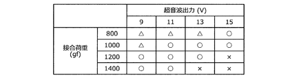
- FIG. 12 shows the result of producing a plurality of the above-described Example 2 under different wire bonding conditions and measuring the bonding quality of the wire 7. As a comparison, FIG.
- Example 2 From the results shown in FIG. 6, in Example 1, when the ultrasonic output of wire bonding is 11 V or more, the bonding load for bonding the wire 7 and the member to be bonded is set to 800 gf to 1400 gf, and the wire bonding super It was confirmed that when the sound wave output is 13 V or more, the bonding strength of the wire 7 can be sufficiently secured by setting the bonding load to 1000 gf to 1400 gf. From the results shown in FIG. 12, in Example 2, the bonding load range in which the bonding strength between the wire 7 and the member to be bonded can be sufficiently secured by setting the ultrasonic output of the wire bonding to 11 V or more.
- FIG. 8 is a characteristic diagram showing the power cycle capability of the semiconductor device according to the embodiment.
- FIG. 8 shows the relationship between the number of cycles of the power cycle and the temperature change ⁇ Tj of the junction temperature of the semiconductor element in Examples 1 and 2 and Conventional Example 1 described above.
- the maximum junction temperature Tjmax of the semiconductor element was 175 ° C. From the results shown in FIG. 8, it was confirmed that Examples 1 and 2 can perform more power cycle cycles than Conventional Example 1 under the use conditions at high temperatures. That is, Examples 1 and 2 were able to increase the power cycle tolerance twice or more than Conventional Example 1.
- FIG. 9 is a cross-sectional view schematically showing a state near the bonding interface of the wire after wire bonding of the semiconductor device according to the embodiment.
- 9A to 9F show wires of a semiconductor device in which Ni plating films having thicknesses of 0.1 ⁇ m, 0.3 ⁇ m, 0.5 ⁇ m, 1 ⁇ m, 3 ⁇ m, and 5 ⁇ m are formed as the front surface metal film 14. 47 shows the vicinity of the bonding interface.
- the Ni plating film 43 is shown by a line segment, and the thickness of the Ni plating film 43 is shown by the thickness of this line segment.
- 9 (e) and 9 (f) the Ni plating film 44 is illustrated by a black solid line, and the thickness of the horizontal line (the width in the depth direction of the semiconductor substrate 41) of the Ni plating film 44 is shown. The film thickness is shown.
- FIG. 9B showing the Ni plating film 43 having a thickness of 0.3 ⁇ m corresponds to the semiconductor device of the first embodiment
- FIG. 9F showing the Ni plating film 44 having a thickness of 5 ⁇ m is the semiconductor device of the second embodiment.
- the Ni plating film 43 was broken by wire bonding, and the AlSi electrode 42 as the front electrode 12 was formed. It was confirmed that it was dispersed at the bonding interface between the wire 47 and the wire 47.
- Example 1 the state in the vicinity of the bonding interface of the wire 47 is that the Ni plating film 43 is broken immediately after the wire bonding, and the wire 47 and the AlSi electrode 42 are directly bonded, and the reference shown in FIG. It became an embodiment of the example, and it was confirmed that it was as shown in FIG. 4C after the power cycle test.
- the Ni plating films 43 having thicknesses of 0.1 ⁇ m, 0.5 ⁇ m, and 1 ⁇ m shown in FIGS. 9A, 9C, and 9D, respectively, are formed immediately after wire bonding, as in the first embodiment.
- the Ni plating film 43 was broken.
- the thickness of the front metal film 14 is 3 ⁇ m or more, preferably 3 ⁇ m to 5 ⁇ m.
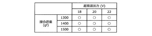
- FIG. 13 is a characteristic diagram showing the bonding quality of another example of the semiconductor device according to the embodiment.
- FIG. 14 is a characteristic diagram showing the bonding quality of another example of a conventional semiconductor device. ⁇ indicates the case where the bonding strength of the wire is sufficiently secured to withstand as a product, ⁇ indicates the case where the bonding strength of the wire is low, and ⁇ indicates the case where the wire peels and causes element destruction Yes.
- Example 3 The result of measuring the bonding strength of the wire 7 in the semiconductor device according to the embodiment (hereinafter referred to as Example 3) in which the wire 7 having a wire diameter of 500 ⁇ m was bonded to the front metal film 14 under different wire bonding conditions.
- a Ni plating film having a thickness of 5 ⁇ m was formed as the front metal film 14.
- the configuration of the third embodiment is the same as that of the second embodiment except that the wire 7 has a different wire diameter.
- the bonding strength of the wire 37 was measured in a conventional semiconductor device (hereinafter referred to as Conventional Example 2) in which a wire 37 having a wire diameter of 500 ⁇ m was bonded to the front electrode 112 under different wire bonding conditions.
- Conventional Example 2 The results are shown in FIG.
- the configuration of Conventional Example 2 is the same as that of the reference example except that the wire 37 has a different wire diameter.
- the thickness of the Ni plating film (front metal film 14) is set to 5.0 ⁇ m, and the wire diameter of the wire 7 is set to 500 ⁇ m. Even if the sound wave output is increased (18 V to 22 V) and the bonding load for bonding the wire 7 and the member to be bonded is increased (1300 gf to 1500 gf), the bonding between the front metal film 14 and the wire 7 is performed. It was confirmed that no bonding failure occurred in the portion and the bonding strength of the wire 7 could be sufficiently secured. On the other hand, from the result shown in FIG.
- the crystal grain size of the wire is controlled so that the recrystallization temperature of the wire is higher than the recrystallization temperature of the conventional aluminum wire, and the hardness of the wire is increased.
- the front electrode can be strengthened by providing the front metal film having a hardness higher than that of the wire on the surface of the front electrode. It can prevent that a crack arises in a surface electrode.
- the front surface metal film functions as a barrier, so even if a crack occurs in the wire, It is possible to prevent the crack from progressing to the front electrode.
- the power cycle resistance can be improved by preventing the surface electrode from cracking and suppressing the cracking from occurring in the wire. Therefore, a highly reliable semiconductor device can be provided.
- the stress applied to the front electrode due to thermal deformation of the wire is increased, but the hardness of the surface of the front electrode is higher than that of the wire. Since the front electrode is strengthened by providing the front metal film, it is possible to prevent the front electrode from being damaged.
- the present invention can be variously changed.
- the dimensions of each part are variously set according to required specifications.
- the semiconductor device and the method for manufacturing the semiconductor device according to the present invention are useful for a semiconductor device having a module structure used for a general-purpose inverter, wind power generation, solar power generation, electric railway, and the like.
Landscapes
- Wire Bonding (AREA)
- Engineering & Computer Science (AREA)
- Manufacturing & Machinery (AREA)
Abstract
Description
実施の形態にかかる半導体装置の構造について説明する。図1は、実施の形態にかかる半導体装置の構造を示す断面図である。図2は、図1の半導体素子の構造を模式的に示す断面図である。図1,2に示すように、実施の形態にかかる半導体装置は、半導体素子(半導体チップ)1と、セラミクス絶縁基板(DCB基板)などの絶縁基板2と、銅(Cu)ベース6と、ワイヤ7とを備えたモジュール構造の半導体装置である。絶縁基板2は、絶縁層3のおもて面側に例えばCuなどからなる回路層4が設けられ、裏面側に裏銅箔5が設けられている。
1a はんだ接合層
2 絶縁基板
3 絶縁層
4 回路層
5 裏銅箔
6 Cuベース
7 ワイヤ
11 半導体基板
12 おもて面電極
13 裏面電極
14 おもて面金属膜
20 ワイヤの接合界面
21 クラック
Claims (8)
- ワイヤボンディングによって半導体素子の電極とワイヤとを電気的に接続してなる半導体装置において、
前記電極の表面に、前記ワイヤよりも硬度が高い金属膜が設けられており、
前記ワイヤは、ワイヤボンディングによって前記金属膜に接合されており、
前記ワイヤの前記金属膜との接合界面の再結晶温度が175℃以上であることを特徴とする半導体装置。 - 前記ワイヤの前記接合界面の結晶粒の粒径は15μm以下であり、
前記ワイヤの前記接合界面から離れた部分は粒径が15μmより大きい結晶粒を含むことを特徴とする請求項1に記載の半導体装置。 - 前記ワイヤの硬度は、前記電極の硬度よりも高いことを特徴とする請求項1に記載の半導体装置。
- 前記金属膜はニッケルめっき膜であることを特徴とする請求項1~3のいずれか一つに記載の半導体装置。
- 前記ニッケルめっき膜の膜厚は3μm~7μmであることを特徴とする請求項4に記載の半導体装置。
- 前記金属膜は銅めっき膜であることを特徴とする請求項1~3のいずれか一つに記載の半導体装置。
- 前記銅めっき膜の膜厚は4.5μm~10.5μmであることを特徴とする請求項6に記載の半導体装置。
- 半導体素子の電極とワイヤとを電気的に接続する半導体装置の製造方法において、
前記ワイヤよりも硬度が高い金属膜を前記電極の表面に設ける工程と、
ワイヤボンディングの超音波振動により前記ワイヤの前記金属膜との接合界面の結晶粒の粒径を15μm以下にして前記ワイヤを前記金属膜に接合する工程と、
を含むことを特徴とする半導体装置の製造方法。
Priority Applications (4)
| Application Number | Priority Date | Filing Date | Title |
|---|---|---|---|
| DE112014002135.0T DE112014002135T5 (de) | 2013-04-25 | 2014-04-23 | Halbleitervorrichtung und Verfahren zum Herstellen einer Halbleitervorrichtung |
| CN201480012154.0A CN105190858B (zh) | 2013-04-25 | 2014-04-23 | 半导体装置及半导体装置的制造方法 |
| JP2015513808A JP6132014B2 (ja) | 2013-04-25 | 2014-04-23 | 半導体装置および半導体装置の製造方法 |
| US14/845,256 US9748186B2 (en) | 2013-04-25 | 2015-09-03 | Semiconductor device and method for manufacturing the semiconductor device |
Applications Claiming Priority (2)
| Application Number | Priority Date | Filing Date | Title |
|---|---|---|---|
| JP2013-092110 | 2013-04-25 | ||
| JP2013092110 | 2013-04-25 |
Related Child Applications (1)
| Application Number | Title | Priority Date | Filing Date |
|---|---|---|---|
| US14/845,256 Continuation US9748186B2 (en) | 2013-04-25 | 2015-09-03 | Semiconductor device and method for manufacturing the semiconductor device |
Publications (1)
| Publication Number | Publication Date |
|---|---|
| WO2014175343A1 true WO2014175343A1 (ja) | 2014-10-30 |
Family
ID=51791911
Family Applications (1)
| Application Number | Title | Priority Date | Filing Date |
|---|---|---|---|
| PCT/JP2014/061457 Ceased WO2014175343A1 (ja) | 2013-04-25 | 2014-04-23 | 半導体装置および半導体装置の製造方法 |
Country Status (5)
| Country | Link |
|---|---|
| US (1) | US9748186B2 (ja) |
| JP (1) | JP6132014B2 (ja) |
| CN (1) | CN105190858B (ja) |
| DE (1) | DE112014002135T5 (ja) |
| WO (1) | WO2014175343A1 (ja) |
Cited By (5)
| Publication number | Priority date | Publication date | Assignee | Title |
|---|---|---|---|---|
| JPWO2016143557A1 (ja) * | 2015-03-10 | 2017-05-25 | 三菱電機株式会社 | パワー半導体装置 |
| JP2017199813A (ja) * | 2016-04-27 | 2017-11-02 | 富士電機株式会社 | 半導体装置及びその製造方法 |
| WO2022163695A1 (ja) * | 2021-01-28 | 2022-08-04 | 三菱電機株式会社 | 半導体装置、電力変換装置および半導体装置の製造方法 |
| JP2023033668A (ja) * | 2021-08-30 | 2023-03-13 | 株式会社 日立パワーデバイス | 半導体装置及びその製造方法 |
| WO2024029286A1 (ja) * | 2022-08-03 | 2024-02-08 | ローム株式会社 | 半導体装置、および、半導体装置の製造方法 |
Families Citing this family (18)
| Publication number | Priority date | Publication date | Assignee | Title |
|---|---|---|---|---|
| US10886250B2 (en) | 2015-07-10 | 2021-01-05 | Invensas Corporation | Structures and methods for low temperature bonding using nanoparticles |
| TWI822659B (zh) | 2016-10-27 | 2023-11-21 | 美商艾德亞半導體科技有限責任公司 | 用於低溫接合的結構和方法 |
| US10515913B2 (en) | 2017-03-17 | 2019-12-24 | Invensas Bonding Technologies, Inc. | Multi-metal contact structure |
| US10446441B2 (en) | 2017-06-05 | 2019-10-15 | Invensas Corporation | Flat metal features for microelectronics applications |
| CN111344840B (zh) * | 2017-11-22 | 2023-07-07 | 三菱电机株式会社 | 半导体装置以及半导体装置的制造方法 |
| JP6698231B2 (ja) * | 2018-02-01 | 2020-05-27 | パナソニック株式会社 | 半導体装置および半導体装置の製造方法 |
| EP3550596B1 (en) * | 2018-04-04 | 2024-09-04 | Infineon Technologies AG | Arrangements and method for providing a wire bond connection |
| US10790262B2 (en) | 2018-04-11 | 2020-09-29 | Invensas Bonding Technologies, Inc. | Low temperature bonded structures |
| US11244916B2 (en) | 2018-04-11 | 2022-02-08 | Invensas Bonding Technologies, Inc. | Low temperature bonded structures |
| US11244920B2 (en) | 2018-12-18 | 2022-02-08 | Invensas Bonding Technologies, Inc. | Method and structures for low temperature device bonding |
| CN110158020B (zh) * | 2019-04-09 | 2020-04-21 | 山东大学 | 一种超声辅助感应加热制备纳米结构氧化膜的方法 |
| WO2021014007A1 (en) * | 2019-07-25 | 2021-01-28 | Abb Power Grids Switzerland Ag | Power semiconductor module |
| US11735523B2 (en) | 2020-05-19 | 2023-08-22 | Adeia Semiconductor Bonding Technologies Inc. | Laterally unconfined structure |
| CN112201628A (zh) * | 2020-08-24 | 2021-01-08 | 株洲中车时代半导体有限公司 | 一种功率模块封装结构及其制备方法 |
| CN116848631A (zh) * | 2020-12-30 | 2023-10-03 | 美商艾德亚半导体接合科技有限公司 | 具有导电特征的结构及其形成方法 |
| US12512425B2 (en) | 2022-04-25 | 2025-12-30 | Adeia Semiconductor Bonding Technologies Inc. | Expansion controlled structure for direct bonding and method of forming same |
| US12545010B2 (en) | 2022-12-29 | 2026-02-10 | Adeia Semiconductor Bonding Technologies Inc. | Directly bonded metal structures having oxide layers therein |
| US12506114B2 (en) | 2022-12-29 | 2025-12-23 | Adeia Semiconductor Bonding Technologies Inc. | Directly bonded metal structures having aluminum features and methods of preparing same |
Citations (5)
| Publication number | Priority date | Publication date | Assignee | Title |
|---|---|---|---|---|
| JP2004179484A (ja) * | 2002-11-28 | 2004-06-24 | Toyota Motor Corp | ワイヤが接合されている半導体装置の製造方法 |
| JP2004200644A (ja) * | 2002-10-22 | 2004-07-15 | Kyocera Corp | 配線基板 |
| JP2009076703A (ja) * | 2007-09-21 | 2009-04-09 | Fuji Electric Device Technology Co Ltd | 半導体装置 |
| JP2010251483A (ja) * | 2009-04-14 | 2010-11-04 | Renesas Electronics Corp | 半導体装置およびその製造方法 |
| JP5159000B1 (ja) * | 2012-06-13 | 2013-03-06 | 田中電子工業株式会社 | 半導体装置接続用アルミニウム合金細線 |
Family Cites Families (8)
| Publication number | Priority date | Publication date | Assignee | Title |
|---|---|---|---|---|
| JPS61163235A (ja) | 1985-01-09 | 1986-07-23 | Toshiba Corp | 半導体素子用ボンデイング線 |
| JPS63148646A (ja) * | 1986-12-12 | 1988-06-21 | Toshiba Corp | 半導体装置 |
| JPH07135234A (ja) | 1993-11-09 | 1995-05-23 | Hitachi Ltd | パワー半導体モジュール |
| JPH088288A (ja) | 1994-06-20 | 1996-01-12 | Hitachi Ltd | 半導体装置 |
| JPH08330710A (ja) * | 1995-06-05 | 1996-12-13 | Nippon Paint Co Ltd | プリント配線板電極部の金属めっき加工方法 |
| JP4696532B2 (ja) * | 2004-05-20 | 2011-06-08 | 株式会社デンソー | パワー複合集積型半導体装置およびその製造方法 |
| JP2008311383A (ja) | 2007-06-14 | 2008-12-25 | Ibaraki Univ | ボンディングワイヤ、それを使用したボンディング方法及び半導体装置並びに接続部構造 |
| CN102244062B (zh) * | 2011-07-26 | 2015-04-22 | 日月光半导体制造股份有限公司 | 半导体封装结构以及半导体封装工艺 |
-
2014
- 2014-04-23 JP JP2015513808A patent/JP6132014B2/ja active Active
- 2014-04-23 DE DE112014002135.0T patent/DE112014002135T5/de active Pending
- 2014-04-23 CN CN201480012154.0A patent/CN105190858B/zh active Active
- 2014-04-23 WO PCT/JP2014/061457 patent/WO2014175343A1/ja not_active Ceased
-
2015
- 2015-09-03 US US14/845,256 patent/US9748186B2/en active Active
Patent Citations (5)
| Publication number | Priority date | Publication date | Assignee | Title |
|---|---|---|---|---|
| JP2004200644A (ja) * | 2002-10-22 | 2004-07-15 | Kyocera Corp | 配線基板 |
| JP2004179484A (ja) * | 2002-11-28 | 2004-06-24 | Toyota Motor Corp | ワイヤが接合されている半導体装置の製造方法 |
| JP2009076703A (ja) * | 2007-09-21 | 2009-04-09 | Fuji Electric Device Technology Co Ltd | 半導体装置 |
| JP2010251483A (ja) * | 2009-04-14 | 2010-11-04 | Renesas Electronics Corp | 半導体装置およびその製造方法 |
| JP5159000B1 (ja) * | 2012-06-13 | 2013-03-06 | 田中電子工業株式会社 | 半導体装置接続用アルミニウム合金細線 |
Cited By (9)
| Publication number | Priority date | Publication date | Assignee | Title |
|---|---|---|---|---|
| JPWO2016143557A1 (ja) * | 2015-03-10 | 2017-05-25 | 三菱電機株式会社 | パワー半導体装置 |
| JP2018037684A (ja) * | 2015-03-10 | 2018-03-08 | 三菱電機株式会社 | パワー半導体装置 |
| JP2017199813A (ja) * | 2016-04-27 | 2017-11-02 | 富士電機株式会社 | 半導体装置及びその製造方法 |
| WO2022163695A1 (ja) * | 2021-01-28 | 2022-08-04 | 三菱電機株式会社 | 半導体装置、電力変換装置および半導体装置の製造方法 |
| JPWO2022163695A1 (ja) * | 2021-01-28 | 2022-08-04 | ||
| JP7555435B2 (ja) | 2021-01-28 | 2024-09-24 | 三菱電機株式会社 | 半導体装置、電力変換装置および半導体装置の製造方法 |
| JP2023033668A (ja) * | 2021-08-30 | 2023-03-13 | 株式会社 日立パワーデバイス | 半導体装置及びその製造方法 |
| JP7619723B2 (ja) | 2021-08-30 | 2025-01-22 | ミネベアパワーデバイス株式会社 | 半導体装置及びその製造方法 |
| WO2024029286A1 (ja) * | 2022-08-03 | 2024-02-08 | ローム株式会社 | 半導体装置、および、半導体装置の製造方法 |
Also Published As
| Publication number | Publication date |
|---|---|
| JPWO2014175343A1 (ja) | 2017-02-23 |
| DE112014002135T5 (de) | 2016-01-14 |
| CN105190858B (zh) | 2018-11-06 |
| JP6132014B2 (ja) | 2017-05-24 |
| US9748186B2 (en) | 2017-08-29 |
| US20150380368A1 (en) | 2015-12-31 |
| CN105190858A (zh) | 2015-12-23 |
Similar Documents
| Publication | Publication Date | Title |
|---|---|---|
| JP6132014B2 (ja) | 半導体装置および半導体装置の製造方法 | |
| JP5159001B1 (ja) | アルミニウム合金ボンディングワイヤ | |
| JP5214936B2 (ja) | 半導体装置 | |
| JP3988735B2 (ja) | 半導体装置及びその製造方法 | |
| JP6056968B2 (ja) | 半導体装置 | |
| CN108367994A (zh) | 铜陶瓷基板、制备铜陶瓷基板的铜半成品及制备铜陶瓷基板的方法 | |
| JPWO2017217145A1 (ja) | はんだ接合部 | |
| TW201325330A (zh) | 配線基板及其製造方法以及半導體裝置 | |
| JP6575386B2 (ja) | 接合体の製造方法、ヒートシンク付パワーモジュール用基板の製造方法、及び、ヒートシンクの製造方法 | |
| CN109075159B (zh) | 半导体装置及其制造方法 | |
| WO2012049893A1 (ja) | 高温半導体素子用平角状銀(Ag)クラッド銅リボン | |
| WO2013005555A1 (ja) | 金属接合構造とその製造方法 | |
| JP6031784B2 (ja) | パワーモジュール用基板及びその製造方法 | |
| TWM666873U (zh) | 封裝結構 | |
| JP2011061105A (ja) | 接続構造、パワーモジュール及びその製造方法 | |
| WO2013058020A1 (ja) | 半導体装置および半導体装置製造方法 | |
| JP4795471B2 (ja) | 電力用半導体素子 | |
| JP2005032833A (ja) | モジュール型半導体装置 | |
| JP2018125354A (ja) | 半導体装置 | |
| JP2017059673A (ja) | 冷却器、パワーデバイス、冷却器の製造方法、およびパワーデバイスの製造方法 | |
| TWM666872U (zh) | 封裝結構 | |
| JP2018137277A (ja) | 銅/アルミニウム接合体の製造方法、絶縁回路基板の製造方法、ヒートシンク付き絶縁回路基板の製造方法 | |
| CN114496967A (zh) | 一种二极管的键合封装结构及其工艺 | |
| JP2016072291A (ja) | 半導体装置 |
Legal Events
| Date | Code | Title | Description |
|---|---|---|---|
| WWE | Wipo information: entry into national phase |
Ref document number: 201480012154.0 Country of ref document: CN |
|
| 121 | Ep: the epo has been informed by wipo that ep was designated in this application |
Ref document number: 14787861 Country of ref document: EP Kind code of ref document: A1 |
|
| ENP | Entry into the national phase |
Ref document number: 2015513808 Country of ref document: JP Kind code of ref document: A |
|
| WWE | Wipo information: entry into national phase |
Ref document number: 112014002135 Country of ref document: DE Ref document number: 1120140021350 Country of ref document: DE |
|
| 122 | Ep: pct application non-entry in european phase |
Ref document number: 14787861 Country of ref document: EP Kind code of ref document: A1 |