WO2014174902A1 - 半導体装置および半導体装置の製造方法 - Google Patents
半導体装置および半導体装置の製造方法 Download PDFInfo
- Publication number
- WO2014174902A1 WO2014174902A1 PCT/JP2014/055378 JP2014055378W WO2014174902A1 WO 2014174902 A1 WO2014174902 A1 WO 2014174902A1 JP 2014055378 W JP2014055378 W JP 2014055378W WO 2014174902 A1 WO2014174902 A1 WO 2014174902A1
- Authority
- WO
- WIPO (PCT)
- Prior art keywords
- layer
- insulating
- wirings
- region
- protective layer
- Prior art date
- Legal status (The legal status is an assumption and is not a legal conclusion. Google has not performed a legal analysis and makes no representation as to the accuracy of the status listed.)
- Ceased
Links
Images









Classifications
-
- H—ELECTRICITY
- H10—SEMICONDUCTOR DEVICES; ELECTRIC SOLID-STATE DEVICES NOT OTHERWISE PROVIDED FOR
- H10D—INORGANIC ELECTRIC SEMICONDUCTOR DEVICES
- H10D86/00—Integrated devices formed in or on insulating or conducting substrates, e.g. formed in silicon-on-insulator [SOI] substrates or on stainless steel or glass substrates
- H10D86/01—Manufacture or treatment
- H10D86/021—Manufacture or treatment of multiple TFTs
-
- H—ELECTRICITY
- H10—SEMICONDUCTOR DEVICES; ELECTRIC SOLID-STATE DEVICES NOT OTHERWISE PROVIDED FOR
- H10D—INORGANIC ELECTRIC SEMICONDUCTOR DEVICES
- H10D86/00—Integrated devices formed in or on insulating or conducting substrates, e.g. formed in silicon-on-insulator [SOI] substrates or on stainless steel or glass substrates
- H10D86/40—Integrated devices formed in or on insulating or conducting substrates, e.g. formed in silicon-on-insulator [SOI] substrates or on stainless steel or glass substrates characterised by multiple TFTs
- H10D86/421—Integrated devices formed in or on insulating or conducting substrates, e.g. formed in silicon-on-insulator [SOI] substrates or on stainless steel or glass substrates characterised by multiple TFTs having a particular composition, shape or crystalline structure of the active layer
-
- H—ELECTRICITY
- H10—SEMICONDUCTOR DEVICES; ELECTRIC SOLID-STATE DEVICES NOT OTHERWISE PROVIDED FOR
- H10D—INORGANIC ELECTRIC SEMICONDUCTOR DEVICES
- H10D86/00—Integrated devices formed in or on insulating or conducting substrates, e.g. formed in silicon-on-insulator [SOI] substrates or on stainless steel or glass substrates
- H10D86/40—Integrated devices formed in or on insulating or conducting substrates, e.g. formed in silicon-on-insulator [SOI] substrates or on stainless steel or glass substrates characterised by multiple TFTs
- H10D86/421—Integrated devices formed in or on insulating or conducting substrates, e.g. formed in silicon-on-insulator [SOI] substrates or on stainless steel or glass substrates characterised by multiple TFTs having a particular composition, shape or crystalline structure of the active layer
- H10D86/423—Integrated devices formed in or on insulating or conducting substrates, e.g. formed in silicon-on-insulator [SOI] substrates or on stainless steel or glass substrates characterised by multiple TFTs having a particular composition, shape or crystalline structure of the active layer comprising semiconductor materials not belonging to the Group IV, e.g. InGaZnO
-
- H—ELECTRICITY
- H10—SEMICONDUCTOR DEVICES; ELECTRIC SOLID-STATE DEVICES NOT OTHERWISE PROVIDED FOR
- H10D—INORGANIC ELECTRIC SEMICONDUCTOR DEVICES
- H10D86/00—Integrated devices formed in or on insulating or conducting substrates, e.g. formed in silicon-on-insulator [SOI] substrates or on stainless steel or glass substrates
- H10D86/40—Integrated devices formed in or on insulating or conducting substrates, e.g. formed in silicon-on-insulator [SOI] substrates or on stainless steel or glass substrates characterised by multiple TFTs
- H10D86/441—Interconnections, e.g. scanning lines
- H10D86/443—Interconnections, e.g. scanning lines adapted for preventing breakage, peeling or short circuiting
-
- H—ELECTRICITY
- H10—SEMICONDUCTOR DEVICES; ELECTRIC SOLID-STATE DEVICES NOT OTHERWISE PROVIDED FOR
- H10D—INORGANIC ELECTRIC SEMICONDUCTOR DEVICES
- H10D86/00—Integrated devices formed in or on insulating or conducting substrates, e.g. formed in silicon-on-insulator [SOI] substrates or on stainless steel or glass substrates
- H10D86/40—Integrated devices formed in or on insulating or conducting substrates, e.g. formed in silicon-on-insulator [SOI] substrates or on stainless steel or glass substrates characterised by multiple TFTs
- H10D86/451—Integrated devices formed in or on insulating or conducting substrates, e.g. formed in silicon-on-insulator [SOI] substrates or on stainless steel or glass substrates characterised by multiple TFTs characterised by the compositions or shapes of the interlayer dielectrics
-
- H—ELECTRICITY
- H10—SEMICONDUCTOR DEVICES; ELECTRIC SOLID-STATE DEVICES NOT OTHERWISE PROVIDED FOR
- H10D—INORGANIC ELECTRIC SEMICONDUCTOR DEVICES
- H10D86/00—Integrated devices formed in or on insulating or conducting substrates, e.g. formed in silicon-on-insulator [SOI] substrates or on stainless steel or glass substrates
- H10D86/40—Integrated devices formed in or on insulating or conducting substrates, e.g. formed in silicon-on-insulator [SOI] substrates or on stainless steel or glass substrates characterised by multiple TFTs
- H10D86/481—Integrated devices formed in or on insulating or conducting substrates, e.g. formed in silicon-on-insulator [SOI] substrates or on stainless steel or glass substrates characterised by multiple TFTs integrated with passive devices, e.g. auxiliary capacitors
-
- H—ELECTRICITY
- H10—SEMICONDUCTOR DEVICES; ELECTRIC SOLID-STATE DEVICES NOT OTHERWISE PROVIDED FOR
- H10D—INORGANIC ELECTRIC SEMICONDUCTOR DEVICES
- H10D86/00—Integrated devices formed in or on insulating or conducting substrates, e.g. formed in silicon-on-insulator [SOI] substrates or on stainless steel or glass substrates
- H10D86/40—Integrated devices formed in or on insulating or conducting substrates, e.g. formed in silicon-on-insulator [SOI] substrates or on stainless steel or glass substrates characterised by multiple TFTs
- H10D86/60—Integrated devices formed in or on insulating or conducting substrates, e.g. formed in silicon-on-insulator [SOI] substrates or on stainless steel or glass substrates characterised by multiple TFTs wherein the TFTs are in active matrices
-
- H—ELECTRICITY
- H10—SEMICONDUCTOR DEVICES; ELECTRIC SOLID-STATE DEVICES NOT OTHERWISE PROVIDED FOR
- H10W—GENERIC PACKAGES, INTERCONNECTIONS, CONNECTORS OR OTHER CONSTRUCTIONAL DETAILS OF DEVICES COVERED BY CLASS H10
- H10W20/00—Interconnections in chips, wafers or substrates
- H10W20/40—Interconnections external to wafers or substrates, e.g. back-end-of-line [BEOL] metallisations or vias connecting to gate electrodes
Definitions
- the present invention relates to a semiconductor device and a method for manufacturing the semiconductor device, for example, an active matrix substrate having TFTs and a display device using the active matrix substrate.
- Display devices such as a liquid crystal display device including an active matrix substrate provided with a switching element for each pixel are widely used.
- An active matrix substrate including a thin film transistor (hereinafter, “TFT”) as a switching element is called a TFT substrate.
- a TFT substrate used in a liquid crystal display device includes, for example, a glass substrate, a plurality of TFTs supported by the glass substrate, a plurality of gate wirings and a plurality of source wirings, and a plurality of pixel electrodes arranged in a matrix.
- the plurality of gate lines are provided so as to extend along the row direction of the display surface, for example, and the plurality of source lines are provided so as to extend along the column direction of the display surface, for example.
- the gate electrode of each TFT is electrically connected to the gate wiring, the source electrode is electrically connected to the source wiring, and the drain electrode is electrically connected to the pixel electrode.
- the thickness and / or dielectric constant of the insulating film is adjusted, and the end of the pixel electrode overlaps with the gate wiring and / or the source wiring.
- a liquid crystal display device in which the pixel aperture ratio is improved by reducing the parasitic capacitance formed thereby (for example, Patent Documents 1 to 4).
- the insulating film is typically formed of an organic insulating material. This is because the organic insulating material has an advantage that it has a lower dielectric constant than an inorganic insulating material and / or is easily formed thick.
- a non-display area (referred to as a “frame area”) is formed around the display area formed by pixels arranged in a matrix on the TFT substrate.
- a terminal portion in addition to a seal portion for bonding two substrates (TFT substrate and counter substrate) disposed so as to face each other with a liquid crystal layer interposed therebetween, a terminal portion, and further a drive circuit Part may be formed.
- the insulating film is formed on almost the entire surface of the display region, but is not formed on at least the terminal portion of the frame region.
- the TFT substrate there are a region where the insulating film is formed and a region where the insulating film is not formed. If the insulating film is thick, a relatively large step is formed.
- a part of the conductive film remains near the edge of the insulating film and is adjacent to each other (gate wiring and / or source wiring). A short circuit may occur between them. This is due to the fact that the resist mask for patterning the conductive film is thicker than above under the step of the insulating film, leaving the resist mask. As described above, the resist mask remaining in the portion to be developed and removed may be referred to as a resist residue.
- Patent Documents 1 and 2 disclose that the generation of resist residue near the edge of the insulating film is suppressed by providing a portion protruding between the wirings in the frame region in the pattern of the insulating film.
- Patent Documents 3 and 4 propose to suppress the generation of resist residues in the vicinity of the edge of the insulating film by preventing the inclination angle of the edge of the insulating film from being steep.
- the present invention has been made to solve the above-described problem, and a short circuit between wirings in a frame region having a simpler structure than that of the prior art or that can be manufactured by a simpler method than before is suppressed.
- An object is to provide a semiconductor device.
- a semiconductor device includes a substrate, a first metal layer including a plurality of first wires supported by the substrate, an insulating layer formed on the first metal layer, and the insulating layer A second metal layer including a plurality of second wirings formed thereon and an insulating protective layer covering a part of each of the plurality of second wirings, wherein the insulating protective layer is formed on the substrate; An insulating protective layer that defines a formed first region and a second region where the insulating protective layer is not formed; and a conductive layer formed on the insulating protective layer. In the cross section including the boundary between the region and the second region, the surface of the insulating layer on the insulating protective layer side has a step between two adjacent second wirings.
- the surface includes a portion protruding toward the insulating protective layer side.
- the protruding portion is formed at a position overlapping at least one of the two second wirings.
- the number of steps between the two second wirings is one.
- the projecting portion is formed between the two second wirings.
- the first metal layer includes an island-like portion straddling the first region and the second region, and the step has a shape reflecting an outline of the island-like portion in the cross section.
- the island-shaped portion is arranged at a position overlapping at least one of the two second wirings.
- the island portion is disposed between the two second wirings.
- the semiconductor device further includes a plurality of switching elements supported by the substrate, wherein each of the plurality of switching elements includes a first contact region, a second contact region, the first contact region, and the second contact region.
- the island-shaped portion is electrically connected to a corresponding first wiring among the plurality of first wirings.
- the semiconductor layer includes an oxide semiconductor.
- the oxide semiconductor may include an In—Ga—Zn—O-based semiconductor.
- the In—Ga—Zn—O-based semiconductor may include a crystalline portion.
- the semiconductor device further includes a driving circuit disposed in the second region, and the plurality of second wirings include second wirings directly connected to the driving circuit.
- the insulating protective layer is a layer made of an organic insulating material.
- a method of manufacturing a semiconductor device includes a step (a) of forming a first metal layer including a plurality of island-shaped portions and a plurality of first wirings on a substrate, and insulation covering the first metal layer.
- a step reflecting the surface is formed on the
- a liquid insulating material is applied on the insulating layer and the second metal layer.
- an organic insulating material is applied on the insulating layer and the second metal layer.
- a semiconductor device and a method for manufacturing the semiconductor device in which a short circuit between wirings in a frame region is suppressed.
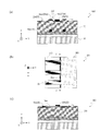
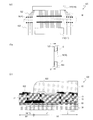
- (A) is typical sectional drawing of TFT substrate 100T by embodiment of this invention
- (b) is a top view of TFT substrate 100T
- (c) is 1st area
- (A) is a figure which shows typically the state with which the material which comprises the conductive layer 90 remains in the boundary vicinity between 1st area
- (A) is a typical top view of TFT substrate 100T
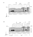
- (b) is sectional drawing which shows the periphery of TFT2 shown to (a).
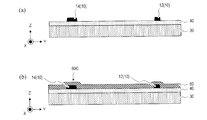
- (A)-(d) is a schematic diagram which shows the outline of the manufacturing method of the TFT substrate by embodiment of this invention.
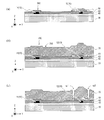
- (A)-(c) is a schematic diagram which shows the outline of the manufacturing method of the TFT substrate by embodiment of this invention.
- (A) And (b) is a schematic diagram which shows the outline of the manufacturing method of the TFT substrate by embodiment of this invention.
- (A) And (b) is a schematic diagram which shows the outline of the manufacturing method of the TFT substrate by embodiment of this invention.
- FIG. (A) And (b) is a schematic diagram which shows the outline of the manufacturing method of the TFT substrate by embodiment of this invention.
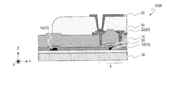
- 4 is a schematic cross-sectional view of a TFT substrate 100B in which a bottom gate type TFT 4 is formed on a substrate 30.
- FIG. (A) And (b) is a schematic diagram which shows the outline of the manufacturing method of the TFT substrate in which the bottom gate type TFT was formed.
- (A)-(c) is a schematic diagram which shows the outline of the manufacturing method of the TFT substrate in which the bottom gate type TFT was formed.
- (A)-(c) is a schematic diagram which shows the outline of the manufacturing method of the TFT substrate in which the bottom gate type TFT was formed.
- (A) And (b) is a schematic diagram which shows the outline of the manufacturing method of the TFT substrate in which the bottom gate type TFT was formed.
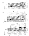
- (A)-(c) is a schematic diagram which shows the process of conductive layer formation in the manufacturing process of TFT substrate 500 shown to FIG.2 (b) and (c).
- (A) And (b) is a schematic diagram which shows TFT substrate 200d by other embodiment of this invention.
- (A) And (b) is a schematic diagram which shows TFT substrate 300d by other embodiment of this invention.
- (A) is typical sectional drawing of TFT substrate 100f by other embodiment of this invention
- (b) is a typical top view of TFT substrate 100e by other embodiment of this invention.
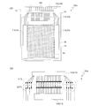
- FIG. 19A is an enlarged view of a portion M indicated by a broken line in FIG. 19B
- FIG. 19B is a cross-sectional view when the TFT substrate 300a is cut along the line UU ′ of FIG. It is.
- (A) is a figure which shows as a comparison the TFT substrate 600 to which the 2nd wiring 22 and the drive circuit 310 were connected via the 1st metal layer 10 in the vicinity of the boundary of 1st area
- (B) is an enlarged view of a portion M indicated by a broken line in (a), and (c) is a cross-sectional view when the TFT substrate 600 is cut along the line UU ′ in (b). It is.
- (A) is a top view which shows the TFT substrate 300b by further another embodiment of this invention
- (b) is an enlarged view of the M section shown with a broken line in (a)
- (c) is It is sectional drawing when the TFT substrate 300b is cut
- a semiconductor device includes a substrate, a first metal layer including a plurality of first wires supported by the substrate, an insulating layer formed on the first metal layer, and an insulating layer formed on the insulating layer.
- a second metal layer including a plurality of second wirings, an insulating protective layer covering a part of each of the plurality of second wirings, and a conductive layer formed on the insulating protective layer.
- the insulating protective layer defines a first region where the insulating protective layer is formed and a second region where the insulating protective layer is not formed on the substrate.
- the surface of the insulating layer on the insulating protective layer side has a step between two adjacent second wirings.
- the surface on the insulating protective layer side of the insulating layer has a step between the two adjacent second wirings. Formation of a leakage path between the second wirings is suppressed.
- the “metal layer” means a layer having conductivity, and is not limited to a layer formed of metal, and includes, for example, a layer formed of metal nitride or metal oxide. Moreover, it is not limited to a single layer, A plurality of layers may be laminated. Below, the TFT substrate used for a liquid crystal display device is illustrated as a semiconductor device.
- FIGS. 1A to 1C a schematic configuration of a TFT substrate according to an embodiment of the present invention will be described. Subsequently, referring to FIGS. 2A to 2C, in the TFT substrate according to the embodiment of the present invention, between two adjacent wirings (typically source wirings) drawn to the second region. The reason why the short circuit is suppressed will be described.
- FIG. 1A is a schematic cross-sectional view of a TFT substrate 100T according to an embodiment of the present invention.
- FIG. 1B is a top view of the TFT substrate 100T.
- FIG. 1A corresponds to a cross-sectional view when the TFT substrate 100T is cut along the line H-H ′ of FIG.
- an X axis, a Y axis, and a Z axis that are orthogonal to each other are shown for reference.
- the X axis and the Y axis are, for example, the horizontal direction and the vertical direction of the display surface of the liquid crystal display device, respectively, and the Z axis is a direction from the TFT substrate to the counter substrate in the liquid crystal display device, for example.
- the X axis, the Y axis, and the Z axis may be shown for reference.
- the TFT substrate 100T includes a substrate 30 and a first metal layer 10 that is supported by the substrate 30 and includes a plurality of first wirings (typically gate wirings) 12. .
- Each of the first wirings 12 includes a gate electrode disposed so as to overlap with the channel region of the corresponding TFT 2. Details of the TFT 2 will be described later.
- An insulating layer 70 is formed on the first metal layer 10, and a second metal layer 20 including a plurality of second wirings (typically source wirings) 22 is formed on the insulating layer 70. Yes.
- An insulating protective layer 80 is formed on the second metal layer 20.
- the insulating protective layer 80 is typically a layer formed from an organic insulating material.
- the insulating protective layer 80 covers a part of each of the second wirings 22. In other words, each of the second wirings 22 has a part exposed without being covered by the insulating protective layer 80.
- a conductive layer (for example, pixel electrode) 90 is formed on the insulating protective layer 80.
- the insulating protective layer 80 covers a part of each of the second wirings 22.
- the first region R1 where the insulating protective layer 80 is formed and the second region R2 where the insulating protective layer 80 is not formed are defined on the substrate 30.
- the first metal layer 10 includes an island-shaped portion 14. This island-shaped part 14 is arrange
- FIG. 1C is a view showing a cross section including a boundary between the first region R1 and the second region R2 of the TFT substrate 100T.
- FIG. 1C corresponds to a cross-sectional view when the TFT substrate 100T is cut along the line V-V ′ of FIG.
- the insulating protective layer 80 is not shown in order to avoid complexity. Note that the illustration of the insulating protective layer may be omitted in other cross-sectional views.
- the surface 70S of the insulating layer 70 on the insulating protective layer 80 side has two adjacent second surfaces. There is a step (shoulder) between the two wirings 22.
- the surface 70S may be referred to as a portion (hereinafter referred to as a “convex portion”) that protrudes toward the insulating protective layer 80 side (the + Z direction in FIG. 1C). ) 70C is included.
- a step Sab1 and a step Sab2 are formed between the second wiring 22a and the second wiring 22b.
- the convex portion 70C is formed on the upper side of the island-shaped portion 14, and the step Sab1 and the step Sab2 have a shape reflecting the outline of the island-shaped portion 14ab. Yes.
- the upper surface of the convex portion may be referred to as a “top surface”.
- FIG. 2A schematically shows a state in which the material constituting the conductive layer 90 remains near the boundary between the first region R1 and the second region R2 (near the edge of the insulating protective layer 80).
- the material constituting the conductive layer 90 remaining in the vicinity of the edge of the insulating protective layer 80 (hereinafter sometimes referred to as “conductive residue”).
- Res is divided into a portion Res1 on the top surface 70T of the convex portion 70C and a portion Res2 on the surface of the portion lower than the top surface 70T. Therefore, even if the conductive residue Res is present, a short circuit between the second wires is suppressed.
- FIGS. 2B and 2C show a top view and a cross-sectional view of a TFT substrate 500 having no step on the surface of the insulating layer 570 as comparative examples.
- FIG. 2C corresponds to a cross-sectional view when the TFT substrate 500 is cut along the line V-V ′ of FIG.
- the surface of the insulating layer 570 does not have a step.
- the conductive residue Res is not divided between the two second wires adjacent to each other, the second wires may be connected by the conductive residue Res. Therefore, in the TFT substrate 500, a leak path may be formed between the second wires in the vicinity of the edge of the insulating protective layer 580.
- FIG. 3A is a schematic top view of the TFT substrate 100T.
- the plurality of first wirings 12 extend along the X direction (for example, the horizontal direction of the display surface), and the plurality of second wirings 22 extend in the Y direction (for example, the display surface). (Vertical direction).
- Each of the plurality of second wirings 22 intersects each of the plurality of first wirings 12 via an insulating layer 70 (not shown).
- a TFT 2 as a switching element is disposed in the vicinity of the intersecting portion of the first wiring 12 and the second wiring 22.
- the auxiliary capacitance wiring 18 may be arranged.
- an auxiliary capacitance is formed in a portion where the auxiliary capacitance wiring 18 and the conductive layer 90 overlap.
- the auxiliary capacitance wiring 18 is formed in the step of forming the plurality of first wirings 12 on the substrate 30. That is, the first metal layer 10 may further include a plurality of auxiliary capacitance lines 18.
- FIG. 3B is a schematic cross-sectional view when the TFT substrate 100T shown in FIG. 3A is cut along the line W-W ′.
- FIG. 3B shows the periphery of the TFT 2 shown in FIG.
- the TFT 2 has a semiconductor layer 50 including a first contact region 51, a second contact region 52, and a channel region 54.
- the channel region 54 is disposed between the first contact region 51 and the second contact region 52.
- the semiconductor layer 50 of the TFT 2 is formed on the substrate 30, and the semiconductor layer 50 and the first wiring 12 are insulated by a gate insulating layer 60 that covers the semiconductor layer 50.
- Each of the plurality of first wirings 12 is disposed so as to overlap the channel region 54 of the corresponding TFT among the plurality of TFTs 2 disposed on the substrate 30.
- each of the plurality of second wirings 22 is electrically connected to the second contact region 52 of the corresponding TFT among the plurality of TFTs 2.
- a scanning signal can be supplied from the first wiring 12 and a display signal can be supplied from the second wiring 22 to each of the plurality of TFTs 2.
- the buffer layer 40 can be disposed between the substrate 30 and the gate insulating layer 60.
- amorphous silicon a-Si
- polycrystalline silicon typically low-temperature polysilicon
- continuous grain boundary crystalline silicon CGS
- the semiconductor layer 50 may be a layer containing an oxide semiconductor.
- the oxide semiconductor includes, for example, an In—Ga—Zn—O-based semiconductor (hereinafter abbreviated as “In—Ga—Zn—O-based semiconductor”).
- a TFT having an In—Ga—Zn—O-based semiconductor layer has high mobility (more than 20 times that of an a-Si TFT) and low leakage current (less than one hundredth of that of an a-Si TFT). It is suitably used as a drive TFT and a pixel TFT.
- a TFT having an In—Ga—Zn—O-based semiconductor layer is used, power consumption of the semiconductor device can be significantly reduced.
- the In—Ga—Zn—O-based semiconductor may be amorphous, may include a crystalline portion, and may have crystallinity.
- a crystalline In—Ga—Zn—O-based semiconductor in which the c-axis is oriented substantially perpendicular to the layer surface is preferable.
- Such a crystal structure of an In—Ga—Zn—O-based semiconductor is disclosed in, for example, Japanese Patent Laid-Open No. 2012-134475. For reference, the entire disclosure of Japanese Patent Application Laid-Open No. 2012-134475 is incorporated herein by reference.
- the semiconductor layer 50 may include another oxide semiconductor instead of the In—Ga—Zn—O-based semiconductor.
- Zn—O based semiconductor ZnO
- In—Zn—O based semiconductor IZO (registered trademark)
- Zn—Ti—O based semiconductor ZTO
- Cd—Ge—O based semiconductor Cd—Pb—O based
- CdO cadmium oxide
- Mg—Zn—O based semiconductors In—Sn—Zn—O based semiconductors (eg, In 2 O 3 —SnO 2 —ZnO), In—Ga—Sn—O based semiconductors, etc. You may go out.
- the second contact region 52 of the semiconductor layer 50 and the second wiring 22 are electrically connected through contact holes provided in the gate insulating layer 60 and the insulating layer 70. ing.
- the first contact region 51 and the drain electrode 21 of the semiconductor layer 50 are electrically connected through contact holes provided in the gate insulating layer 60 and the insulating layer 70.
- the drain electrode 21 is formed in the step of forming the second wiring 22. That is, the second metal layer 20 typically has a drain electrode 21 corresponding to each TFT.
- the conductive layer 90 is electrically connected to the drain electrode 21 through a contact hole vp provided in the insulating protective layer 80.
- the conductive layer 90 is typically configured as a transparent electrode.
- the TFT substrate 100T may be a TFT substrate used in, for example, a twisted nematic (TN) mode, a super twisted nematic (STN) mode, or an optically compensated bend (OCB) mode.
- the TFT substrate 100T may be a TFT substrate used in a liquid crystal display device that operates in a lateral electric field mode such as an In-Plane Switching (IPS) mode or a Ringe Field Switching (FFS) mode. Therefore, the conductive layer 90 may not be transparent.
- IPS In-Plane Switching
- FFS Ringe Field Switching
- a substrate 30 for example, a glass substrate
- the buffer layer 40 may be formed on the substrate 30.
- An example of a material constituting the buffer layer 40 is SiO 2 or SiN.
- the buffer layer 40 may be a stacked body of SiO 2 and SiNO.
- the buffer layer 40 can be formed by, for example, CVD (Chemical Vapor Deposition).
- the thickness of the buffer layer 40 is, for example, 100 nm to 400 nm.
- the semiconductor layer 50 is formed on the substrate 30.
- a silicon film is formed on the substrate 30 by CVD.
- the thickness of the silicon film at this time is, for example, 30 nm to 100 nm.
- a photoresist layer covering a predetermined region of the silicon film is formed by photolithography.
- the portion of the silicon film that is not covered with the photoresist layer is removed by dry etching.
- a gate insulating layer 60 covering the entire surface of the substrate 30 is formed.
- An example of a material constituting the gate insulating layer 60 is SiO 2 or SiNx.
- the gate insulating layer 60 may be a stacked body of these.
- the gate insulating layer 60 can be formed by, for example, CVD.
- the thickness of the gate insulating layer 60 is, for example, 50 nm to 200 nm.
- a metal film (conductor film) 10B is formed on the gate insulating layer 60 by sputtering or the like.
- the material constituting the metal film 10B are W, Ta, TaN, Mo, MoW, Ti, and Al.
- the metal film 10B may be a laminated film in which two or more of these are laminated.
- the thickness of the metal film 10B is, for example, 200 nm to 500 nm.
- first wirings 12 and a plurality of island-like portions 14 are formed on the gate insulating layer 60 (see FIG. 4D).
- Auxiliary capacitance wiring 18 as shown in FIG. 3A may be formed together with the plurality of first wirings 12 and the plurality of island-like portions 14. In this way, the first metal layer 10 having a plurality of first wirings 12 and a plurality of island-like portions 14 is obtained.
- the island-shaped part 14 is formed so as to straddle the region to be the first region R1 and the region to be the second region R2.
- an insulating layer 70 covering the entire surface of the first metal layer 10 is formed.
- the material constituting the insulating layer 70 are SiO 2 , SiNx, or SiNxOy.
- the insulating layer 70 may be a laminated film in which two or more of these are laminated.
- the insulating layer 70 can be formed by, for example, CVD.
- the thickness of the insulating layer 70 is, for example, 300 nm to 1000 nm.
- the insulating layer 70 is provided with a convex portion 70C.
- the material constituting the insulating layer 70 is deposited on the upper surface of the gate insulating layer 60 and the upper surface of the island-shaped portion 14. Therefore, the shape of the convex portion 70 ⁇ / b> C reflects the shape of the island-shaped portion 14.
- a step reflecting the shape of the island-like portion 14 is formed on the surface 70 ⁇ / b> S of the insulating layer 70.
- contact holes vp1 and vp2 are formed in the gate insulating layer 60 and the insulating layer 70 by dry etching or wet etching (see FIG. 5B).
- the second metal layer 20 including the plurality of second wirings 22 is formed on the insulating layer 70 (see FIG. 5C). More specifically, a metal film (conductor film) is formed on the insulating layer 70 by sputtering or the like, and the metal film is patterned by applying photolithography and etching. Examples of metal films are Ti / Al (upper layer / lower layer) laminated film, Ti / Al / Ti laminated film, TiN / Al / TiN laminated film, Mo / Al—Nd / Mo laminated film, Mo / Al / Mo. . The thickness of the metal film is, for example, 100 nm to 500 nm.
- the drain electrode 21 is formed along with the formation of the second wiring 22.
- the drain electrode 21 is electrically connected to the first contact region of the semiconductor layer 50 through the contact hole vp1.
- the second wiring 22 is electrically connected to the second contact region of the semiconductor layer 50 through the contact hole vp2.
- an insulating material 80R is applied on the insulating layer 70 and the second metal layer 20.
- the insulating material 80R is typically a liquid insulating material.
- an organic insulating material typically a photosensitive resin
- a spin-on-glass material may be applied on the insulating layer 70 and the second metal layer 20.
- the insulating material 80R is cured and patterned to form the insulating protective layer 80 (see FIG. 6B).
- the thickness of the insulating protective layer 80 is, for example, 1 ⁇ m to 3 ⁇ m. Note that a contact hole vp is provided in a portion overlapping the drain electrode 21 by patterning.
- the insulating protective layer 80 substantially covers the entire display area.
- the first region R1 region where the insulating protective layer 80 is formed
- the second region R2 region where the insulating protective layer 80 is not formed
- each of the plurality of second wirings 22 extends from the display area to the frame area. Therefore, the insulating protective layer 80 covers a part of each of the plurality of second wirings 22 (see FIG. 1B). Further, as shown in FIG. 6B, the insulating protective layer 80 has an overlap with a part of each of the plurality of island portions 14.
- a step is formed on the surface of the insulating layer 70 on the insulating protective layer 80 side in the cross section including the boundary between the first region R1 and the second region R2.
- the boundary between the first region R1 and the second region R2 is not limited to a linear shape, and may be a curved shape.
- an electrode film 90B is formed on the insulating protective layer 80 by sputtering or the like.
- the material constituting the electrode film 90B are ITO, IZO, and ZnO.
- the thickness of the electrode film 90B is, for example, 30 nm to 150 nm.
- the electrode film 90B is also formed on the bottom surface (upper surface of the drain electrode 21) and the inner peripheral surface of the contact hole vp.
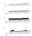
- a resist 92 is applied on the electrode film 90B (see FIG. 7B), and the resist 92 is patterned by photolithography (see FIG. 8A). Thereafter, the portion of the electrode film 90B that is not covered with the resist 92 is removed by wet etching. Thereby, the conductive layer 90 is formed on the insulating protective layer 80 (see FIG. 8B). After the wet etching, the resist 92 is removed to obtain the TFT substrate 100T according to the embodiment of the present invention.
- a plurality of island portions are formed when a plurality of first wirings (typically gate wirings) are formed. That is, a semiconductor device in which a short circuit between the second wirings (typically source wirings) in the frame region is suppressed can be manufactured without greatly changing an existing manufacturing process.
- first wirings typically gate wirings
- FIG. 9 shows a schematic cross section of a TFT substrate 100B in which a bottom gate type TFT 4 is formed on a substrate 30.
- a metal film is formed on the substrate 30, and the metal film is patterned to form the first metal film 10 having a plurality of first wirings 12 and a plurality of island-like portions 14 on the substrate 30 (FIG. 10 (a)).
- the island-shaped part 14 is formed so as to straddle the region to be the first region R1 and the region to be the second region R2.
- the buffer layer 40 may be formed on the substrate 30 in advance.
- a gate insulating layer 60 covering the substrate 30 and the first metal layer 10 is formed by, for example, CVD.
- the material constituting the gate insulating layer 60 is deposited on the upper surface of the substrate 30 (or the buffer layer 40) and the upper surface of the island-shaped portion 14. Therefore, the gate insulating layer 60 is formed with a convex portion 60 ⁇ / b> C reflecting the shape of the island-shaped portion 14.
- a semiconductor layer 50 is formed on the gate insulating layer 60.
- the channel region of the semiconductor layer 50 is formed so as to overlap with the first wiring 12.
- an insulating layer 70 covering the semiconductor layer 50 and the gate insulating layer 60 is formed by, for example, CVD.
- the convex portion 60C reflecting the shape of the island-shaped portion 14 is formed on the gate insulating layer 60
- the convex portion 70C reflecting the shape of the convex portion 60C is formed on the insulating layer 70. . That is, in the process of forming the insulating layer 70, a step reflecting the shape of the island-like portion 14 is formed on the surface 70 ⁇ / b> S of the insulating layer 70.
- contact holes vp 1 and vp 2 are formed in the insulating layer 70.
- the subsequent steps are almost the same as those for manufacturing the TFT substrate 100T. That is, the second metal layer 20 including the plurality of second wirings 22 is formed on the insulating layer 70 (see FIG. 12A). Along with the formation of the second wiring 22, the drain electrode 21 is also formed.
- an insulating material 80R is applied on the insulating layer 70 and the second metal layer 20 (see FIG. 12B).
- photolithography is applied to cure and pattern the insulating material 80R to form the insulating protective layer 80 (see FIG. 12C).
- an electrode film 90B is formed on the insulating protective layer 80 by sputtering or the like, and a resist 92 is applied on the electrode film 90B. Further, the resist 92 is patterned by photolithography (see FIG. 13A). Thereafter, the portion of the electrode film 90B that is not covered with the resist 92 is removed by wet etching (see FIG. 13B). After the wet etching, the resist 92 is removed to obtain the TFT substrate 100B as shown in FIG.
- FIGS. 14 (a) to 14 (c) are schematic views showing a conductive layer forming step in the manufacturing process of the TFT substrate 500 shown in FIGS. 2 (b) and 2 (c). As shown in FIGS. 14A to 14C, the TFT substrate 500 does not have a step on the surface of the insulating layer 570.
- an insulating protective layer 580 is formed on the insulating layer 570.
- the insulating protective layer 580 covers at least a part of the insulating layer 570.
- the first region R1 and the second region R2 are defined on the substrate (not shown) that supports the insulating layer 570 and the insulating protective layer 580.
- the electrode film 590B is formed on the insulating protective layer 580 after the insulating protective layer 580 is formed. As shown in FIG. 14A, the electrode film 590B is also formed in a portion of the insulating layer 570 that is not covered with the insulating protective layer 580. After the formation of the electrode film 590B, a resist 92 is applied on the electrode film 590B. As shown in FIG. 14A, the resist 92 is applied to the entire surface of the electrode film 590B. After the application of the resist 92, the resist 92 is patterned by photolithography.
- the resist 92 is thicker than the other portions (FIG. 14 (a) arrow Tr).
- the exposure amount to the resist 92 tends to be insufficient near the edge of the insulating protective layer 580.
- the exposure amount is likely to be insufficient near the edge of the insulating protective layer 580, and thus a resist residue R92 may be generated near the edge of the insulating protective layer 580 (see FIG. 14B).
- the electrode film 590B covered with the resist residue R92 remains without being removed by etching (see FIG. 14C).
- the conductive residue Res is formed in the vicinity of the edge of the insulating protective layer 580.
- the electrode film 590B in the vicinity of the edge of the insulating protective layer 580 is thicker than other portions (arrow Tc in FIG. 14A). Therefore, even if the resist residue R92 does not exist, the electrode film 590B may remain after etching in the vicinity of the edge of the insulating protective layer 580.
- Patent Documents 1 to 4 described above it is proposed to prevent the formation of a leak path between adjacent source wirings by suppressing the generation of resist residues.
- the shape of the organic insulating film must be controlled by photolithography, and the generation of resist residues may not be sufficiently suppressed.
- the conductive residue is divided by the step. Therefore, even when a conductive residue is present, the formation of a leakage path between the second wirings can be suppressed.
- the step on the surface of the insulating layer is formed by forming an island-shaped portion when forming the first metal film. Therefore, the formation of a leak path can be suppressed without complicating existing processes.
- 15A and 15B are schematic views showing a TFT substrate 200d according to another embodiment of the present invention.
- 15A corresponds to a top view of the TFT substrate 200d
- FIG. 15B corresponds to a cross-sectional view when the TFT substrate 200d is cut along the line VV ′ in FIG. 15A. To do.
- each of the plurality of island portions 14 and each of the plurality of second wirings 22 are arranged to overlap each other. That is, as shown in FIG. 15B, each second wiring 22 is formed on the top surface of the convex portion 70C.
- the convex portion 70C is formed between the two second wirings (see, for example, FIG. 1C).
- the island-like portion 14 is disposed between the two second wirings.
- the convex portion 70 ⁇ / b> C may be formed at a position overlapping the second wiring 22.
- the number of steps between the two second wirings is two. As described above, if a step is formed between the two second wirings, the conductive residue can be divided by the step.
- FIGS. 16A and 16B are schematic views showing a TFT substrate 300d according to another embodiment of the present invention.
- 16A corresponds to a top view of the TFT substrate 300d
- FIG. 16B corresponds to a cross-sectional view when the TFT substrate 300d is cut along the line VV ′ of FIG. 16A. To do.
- the TFT substrate 300d is common to the TFT substrate 200d shown in FIGS. 15A and 15B in that the island-shaped portion 14 and the second wiring 22 are disposed so as to overlap each other.
- the TFT substrate 300 d is different from the TFT substrate 200 d in that island portions 14 are arranged every other plurality of second wirings 22.
- the convex portion 70C only needs to be formed at a position overlapping at least one of the two second wirings. That is, the island portion 14 may be disposed at a position overlapping at least one of the two second wirings.
- FIG. 17A is a schematic cross-sectional view of a TFT substrate 100f according to another embodiment of the present invention.
- the lower wiring 16 is disposed on the gate insulating film 60.
- the lower wiring 16 is formed in the step of forming the plurality of first wirings 12 on the substrate 30. That is, the first metal layer 10 may further include the lower wiring 16.
- the lower wiring 16 may be a wiring connected to the auxiliary capacitance wiring 18. Alternatively, the lower wiring 16 may be a part of the first wiring 12.
- the lower wiring 16 can be connected to a peripheral circuit such as a driver circuit by extending in the X direction (vertical direction on the paper surface) in FIG. 17, for example.
- the lower wiring 16 and the second wiring 22 are electrically connected through a contact hole provided in the insulating layer 70.
- the lower wiring 16 may be formed on the gate insulating film and connected to the second wiring 22 disposed on the insulating layer 70.
- FIG. 17B is a schematic top view of a TFT substrate 100e according to another embodiment of the present invention.
- the configuration of the cross section when the TFT substrate 100e is cut along the line V-V 'of FIG. 17B is substantially the same as the configuration shown in FIG.
- the island portion 14 may be extended to connect the island portion 14 and the first wiring 12 (not shown).
- the island portion 14 can be electrically connected to the corresponding first wiring among the plurality of first wirings 12.
- the first wiring 12 may be extended to the second region R2, and a step may be formed on the surface 70S of the insulating layer 70. You may connect the island-shaped part 14 and the auxiliary capacity wiring 18 (not shown).
- FIGS. 15B and 16B are schematic top views of a TFT substrate 200e and a TFT substrate 300e according to another embodiment of the present invention, respectively.
- each of the plurality of island-like portions 14 and each of the plurality of second wirings 22 may be arranged to overlap each other. Further, as shown in FIG. 18B, the island-like portions 14 may be arranged every other plurality of second wirings 22.
- FIG. 19A is a top view showing a TFT substrate 300a according to still another embodiment of the present invention.
- the TFT substrate 300a is a TFT substrate having a so-called monolithic structure in which a gate driver circuit and a source driver circuit are integrally formed on the substrate.
- two gate driver circuits 314 and one source driver circuit 316 are arranged on three sides of the rectangular display region Rd.
- the gate driver circuit 314 and the source driver circuit 316 are covered with an insulating protective layer 80.
- the wiring group led out from the gate driver circuit 314 and the source driver circuit 316 is connected to the controller 312 disposed in the second region R2.
- the controller 312 is, for example, a timing controller.
- the controller 312 is connected to a terminal 320 for connection with an external circuit.
- the gate driver circuit 314, the source driver circuit 316, the controller 312 and the like may be collectively referred to as a driver circuit 310.
- the controller 312 may be a discrete component or a circuit integrally formed on the substrate. Either one or both of the gate driver circuit 314 and the source driver circuit 316 may be discrete components.
- the controller 312 may be disposed in the first region R1. That is, the controller 312 may be covered with the insulating protective layer 80. Either one or both of the gate driver circuit 314 and the source driver circuit 316 may be arranged in the second region R2.
- the arrangement of the drive circuit 310 is arbitrary.
- the gate driver circuit 314 and the source driver circuit 316 can be integrated at a position corresponding to one side of the rectangular display region Rd.
- FIG. 19 (b) is an enlarged view of a part of FIG. 19 (a).
- a part of the plurality of second wirings 22 arranged on the insulating layer 70 straddles the boundary between the first region R1 and the second region R2 (the edge of the insulating protective layer 80). 312 is connected.
- every other plurality of second wirings 22 drawn in parallel from the first region R1 toward the second region R2 are directly connected to the controller 312.
- a mode in which the second wiring 22 straddling the edge of the insulating protective layer 80 is connected to the drive circuit may be referred to as “directly connected”.
- the second wiring 22 straddling the edge of the insulating protective layer 80 is connected to the drive circuit via another conductive layer such as the first metal layer 10 in the first region R1 and / or the second region R2. It does not exclude the aspect which exists.
- FIG. 20 (a) is an enlarged view of a portion M indicated by a broken line in FIG. 19 (b).
- FIG. 20A a part of the second wiring 22 directly connected to the controller 312 is shown enlarged.
- FIG. 20B is a cross-sectional view of the TFT substrate 300a taken along the line U-U ′ of FIG.
- the TFT 6 shown in FIG. 20B is a driving TFT included in the gate driver circuit 314, for example.
- the second wiring 22 does not pass through the first metal layer 10 disposed below the insulating layer 70.
- controller 312 drive circuit 310 may be directly connected. Thereby, wiring resistance can be reduced.
- the second wiring 22 and the drive circuit 310 are directly connected without passing through another conductive layer such as the first metal layer 10 or the like. The reason why the wiring resistance can be reduced will be described.
- FIG. 21A shows, as a comparison, a TFT substrate 600 in which the second wiring 22 and the drive circuit 310 are connected via the first metal layer 10 in the vicinity of the boundary between the first region R1 and the second region R2.
- FIG. 21B is an enlarged view of a portion M indicated by a broken line in FIG.
- FIG. 21C is a cross-sectional view of the TFT substrate 600 taken along the line U-U ′ of FIG.
- the second wiring 622 in the first region R1 is connected to the connection portion c1, the island-like portion 14 and the connection at the boundary between the first region R1 and the second region R2. Via the part c2, it is connected to the second wiring 622 in the second region R2.
- the second metal layer 20 having the second wiring is made of, for example, a metal material containing Al, and its sheet resistance is about 0.1 ⁇ / ⁇ .
- the first metal layer 10 having an island-shaped portion is formed of, for example, Mo, W, or the like.
- the sheet resistance of the first metal layer 10 is about 0.5 ⁇ / ⁇ , which is higher than the sheet resistance of the second metal layer 20. Therefore, when the first metal layer 10 is passed in the vicinity of the boundary between the first region R1 and the second region R2, the wiring resistance becomes higher than when the second wiring and the drive circuit 310 are directly connected. Moreover, the contact resistance between the connection part c1 and the connection part c2, and the island-like part 14 also arises.
- the wiring resistance can be reduced by directly connecting the second wiring 22 and the drive circuit 310 without going through the first metal layer 10.
- the second wiring 22 and the island portion 14 are connected by, for example, the connection portion c1 and the connection portion c2, and the potential of the second wiring 22 and the island portion 14 are connected. May be equal to each other.
- the wiring that is not directly connected to the controller 312 (drive circuit 310) among the plurality of second wirings 22 straddles the boundary between the first region R1 and the second region R2.
- all of the plurality of second wirings 22 drawn in parallel from the first region R1 toward the second region R2 may be directly connected to the drive circuit 310. Thereby, the wiring resistance as the whole semiconductor device can be further reduced.
- FIG. 22A is a top view showing a TFT substrate 300b according to still another embodiment of the present invention.
- FIG.22 (b) is an enlarged view of the M section shown with a broken line in Fig.22 (a).
- FIG. 22B two adjacent second wirings 22a and 22b are enlarged.
- FIG. 22C is a cross-sectional view of the TFT substrate 300b taken along the line U-U 'of FIG.
- the second wiring 22a is The first metal layer 10 disposed below the insulating layer 70 is not directly connected to the drive circuit 310.
- the second wiring 22 b is connected to the drive circuit 310 via the first metal layer 10 disposed below the insulating layer 70.
- the island-like portion 14 connected to the second wiring 22b has a bent shape, and a part thereof is formed to overlap the second wiring 22a. Yes.
- the island-like portion connected to one of the two second wirings adjacent to each other may have a shape overlapping the other. Also in this case, the effect of reducing the wiring resistance can be obtained as in the case of the TFT substrate 300a.
- the island-like portion connected to one of two adjacent second wirings overlaps the other is shown.
- the island-like portion connected to one of the two second wirings that are not adjacent to each other may have a shape that overlaps the other.
- the island-like portion (first metal layer) arranged so as to overlap with any second wiring may be a wiring that is not connected to another second wiring.
- the surface of the insulating layer 70 on the insulating protective layer 80 side is adjacent to the two second wirings 22 adjacent to each other. There is a step between them. Therefore, the formation of a leakage path between two adjacent second wirings 22 is suppressed. Therefore, in order to prevent a short circuit between the second wirings 22, it is necessary to connect the second wiring 22 and the drive circuit 310 via the first metal layer 10 in the vicinity of the boundary between the first region R1 and the second region R2. There is no. Thereby, the wiring resistance as the whole semiconductor device can be reduced. Furthermore, it is also possible to configure the intervals between the plurality of second wirings 22 in the vicinity of the boundary between the first region R1 and the second region R2.
- a TFT substrate used in a liquid crystal display device is exemplified as the semiconductor device.
- the semiconductor device may be a TFT substrate used in a display device other than the liquid crystal display device.
- the semiconductor device may be, for example, a TFT substrate used for a display device such as an organic EL (electroluminescence) display device or an electrophoretic display device.
- the embodiments of the present invention can be widely applied to active matrix substrates, display devices, and the like. In particular, it is suitably applied to a display device having high-definition pixels.
Landscapes
- Liquid Crystal (AREA)
- Thin Film Transistor (AREA)
- Devices For Indicating Variable Information By Combining Individual Elements (AREA)
- Internal Circuitry In Semiconductor Integrated Circuit Devices (AREA)
- Engineering & Computer Science (AREA)
- Manufacturing & Machinery (AREA)
- Chemical & Material Sciences (AREA)
- Crystallography & Structural Chemistry (AREA)
Abstract
Description
本発明の実施形態による半導体装置は、基板と、基板に支持された、複数の第1配線を含む第1メタル層と、第1メタル層上に形成された絶縁層と、絶縁層上に形成された、複数の第2配線を含む第2メタル層と、複数の第2配線のそれぞれの一部分を覆う絶縁性保護層と、絶縁性保護層上に形成された導電層とを備える。絶縁性保護層は、基板上に、絶縁性保護層が形成された第1領域と、絶縁性保護層が形成されていない第2領域とを規定する。第1領域と第2領域との間の境界を含む断面において、絶縁層の絶縁性保護層側の表面は、互いに隣接する2つの第2配線の間に段差を有する。第1領域と第2領域との間の境界を含む断面において、絶縁層の絶縁性保護層側の表面が、互いに隣接する2つの第2配線の間に段差を有するので、互いに隣接する2つの第2配線の間におけるリーク経路の形成が抑制される。なお、本明細書において、「メタル層」は、導電性を有する層を意味し、金属で形成されている層に限られず、例えば金属窒化物や金属酸化物で形成されている層を含み、また、単一の層に限定されず、複数の層が積層されたものであってもよい。以下では、半導体装置として、液晶表示装置に用いられるTFT基板を例示する。
次に、図4~図8を参照して、本発明の実施形態による半導体装置の製造方法を説明する。ここでは、基板上にトップゲート型のTFTが形成されたTFT基板の製造方法を例示する。基板上にボトムゲート型のTFTが形成されたTFT基板の製造方法の例については後述する。
10 第1メタル層
12 第1配線
14 島状部
20 第2メタル層
22 第2配線
30 基板
50 半導体層
70 絶縁層
80 絶縁性保護層
90 導電層
310 駆動回路
Claims (12)
- 基板と、
前記基板に支持された、複数の第1配線を含む第1メタル層と、
前記第1メタル層上に形成された絶縁層と、
前記絶縁層上に形成された、複数の第2配線を含む第2メタル層と、
前記複数の第2配線のそれぞれの一部分を覆う絶縁性保護層であって、前記基板上に、前記絶縁性保護層が形成された第1領域と、前記絶縁性保護層が形成されていない第2領域とを規定する絶縁性保護層と、
前記絶縁性保護層上に形成された導電層と
を備え、
前記第1領域と前記第2領域との間の境界を含む断面において、前記絶縁層の前記絶縁性保護層側の表面は、互いに隣接する2つの第2配線の間に段差を有する、半導体装置。 - 前記表面は、前記絶縁性保護層側に向けて突出する部分を含む、請求項1に記載の半導体装置。
- 前記突出する部分は、前記2つの第2配線のうちの少なくとも一方に重なる位置に形成されている、請求項2に記載の半導体装置。
- 前記2つの第2配線の間にある段差の数は、1である、請求項1から3のいずれかに記載の半導体装置。
- 前記突出する部分は、前記2つの第2配線の間に形成されている、請求項2に記載の半導体装置。
- 前記第1メタル層は、前記第1領域と前記第2領域とに跨がる島状部を含み、
前記段差は、前記断面における前記島状部の輪郭が反映された形状を有する、請求項1から5のいずれかに記載の半導体装置。 - 前記基板に支持された複数のスイッチング素子をさらに備え、
前記複数のスイッチング素子のそれぞれは、第1コンタクト領域、第2コンタクト領域および前記第1コンタクト領域と前記第2コンタクト領域との間に配置されたチャネル領域を含む半導体層を有し、
前記複数の第1配線のそれぞれは、前記複数のスイッチング素子のうち、対応するスイッチング素子の前記チャネル領域と重なるように配置されており、
前記島状部は、前記複数の第1配線のうち、対応する第1配線に電気的に接続されている、請求項6に記載の半導体装置。 - 前記第2領域に配置された駆動回路をさらに備え、
前記複数の第2配線は、前記駆動回路と直接に接続された第2配線を含む、請求項1から7のいずれかに記載の半導体装置。 - 前記絶縁性保護層は、有機絶縁性材料から構成された層である、請求項1から8のいずれかに記載の半導体装置。
- 複数の島状部および複数の第1配線を含む第1メタル層を基板上に形成する工程(a)と、
前記第1メタル層を覆う絶縁層を形成する工程(b)と、
複数の第2配線を含む第2メタル層を前記絶縁層上に形成する工程(c)と、
絶縁性材料を前記絶縁層上および前記第2メタル層上に付与する工程(d)と、
前記絶縁性材料を硬化させた後にパターニングすることによって、前記複数の第2配線のそれぞれにおける一部分を覆い、かつ前記複数の島状部のそれぞれにおける一部分との重なりを有する絶縁性保護層を形成する工程(e)と、
前記絶縁性保護層上に導電層を形成する工程(f)と
を含み、
前記工程(b)は、前記複数の島状部の形状を反映した段差を前記絶縁層の表面に形成する工程を含む、半導体装置の製造方法。 - 前記工程(d)において、液体状の絶縁性材料が前記絶縁層上および前記第2メタル層上に付与される、請求項10に記載の半導体装置の製造方法。
- 前記工程(d)において、有機絶縁性材料が前記絶縁層上および前記第2メタル層上に付与される、請求項10または11に記載の半導体装置の製造方法。
Priority Applications (3)
| Application Number | Priority Date | Filing Date | Title |
|---|---|---|---|
| JP2015513605A JP6041984B2 (ja) | 2013-04-25 | 2014-03-04 | 半導体装置および半導体装置の製造方法 |
| CN201480023469.5A CN105144364B (zh) | 2013-04-25 | 2014-03-04 | 半导体装置和半导体装置的制造方法 |
| US14/786,650 US9583515B2 (en) | 2013-04-25 | 2014-03-04 | Semiconductor device including substrate which is used in display devices |
Applications Claiming Priority (2)
| Application Number | Priority Date | Filing Date | Title |
|---|---|---|---|
| JP2013-092963 | 2013-04-25 | ||
| JP2013092963 | 2013-04-25 |
Publications (1)
| Publication Number | Publication Date |
|---|---|
| WO2014174902A1 true WO2014174902A1 (ja) | 2014-10-30 |
Family
ID=51791487
Family Applications (1)
| Application Number | Title | Priority Date | Filing Date |
|---|---|---|---|
| PCT/JP2014/055378 Ceased WO2014174902A1 (ja) | 2013-04-25 | 2014-03-04 | 半導体装置および半導体装置の製造方法 |
Country Status (4)
| Country | Link |
|---|---|
| US (1) | US9583515B2 (ja) |
| JP (1) | JP6041984B2 (ja) |
| CN (1) | CN105144364B (ja) |
| WO (1) | WO2014174902A1 (ja) |
Cited By (2)
| Publication number | Priority date | Publication date | Assignee | Title |
|---|---|---|---|---|
| WO2017099024A1 (ja) * | 2015-12-09 | 2017-06-15 | シャープ株式会社 | アクティブマトリクス基板およびそれを備える液晶表示パネル |
| JP2022119776A (ja) * | 2017-10-30 | 2022-08-17 | 株式会社ジャパンディスプレイ | 半導体装置 |
Families Citing this family (4)
| Publication number | Priority date | Publication date | Assignee | Title |
|---|---|---|---|---|
| CN104392999B (zh) * | 2014-09-30 | 2017-03-29 | 合肥京东方光电科技有限公司 | 一种阵列基板及其制作方法、显示装置 |
| US10607533B2 (en) * | 2018-08-03 | 2020-03-31 | Kyocera Corporation | Display apparatus with light emitting portions |
| CN113644085B (zh) * | 2020-08-14 | 2023-06-02 | 友达光电股份有限公司 | 电子装置及电子装置的制造方法 |
| CN113937112A (zh) * | 2021-10-12 | 2022-01-14 | 京东方科技集团股份有限公司 | 阵列基板、显示面板及显示装置 |
Citations (5)
| Publication number | Priority date | Publication date | Assignee | Title |
|---|---|---|---|---|
| JPH1020339A (ja) * | 1996-07-02 | 1998-01-23 | Sharp Corp | アクティブマトリクス基板 |
| JPH1124101A (ja) * | 1997-07-01 | 1999-01-29 | Matsushita Electric Ind Co Ltd | アクティブ素子アレイ基板およびその製造方法 |
| JP2002351354A (ja) * | 2001-05-18 | 2002-12-06 | Internatl Business Mach Corp <Ibm> | 薄膜トランジスタ・アレイ基板、薄膜トランジスタ・アレイ基板の製造方法および表示装置 |
| WO2013021866A1 (ja) * | 2011-08-09 | 2013-02-14 | シャープ株式会社 | 表示装置 |
| WO2014061531A1 (ja) * | 2012-10-16 | 2014-04-24 | シャープ株式会社 | 基板装置及びその製造方法 |
Family Cites Families (15)
| Publication number | Priority date | Publication date | Assignee | Title |
|---|---|---|---|---|
| JP3097841B2 (ja) | 1997-11-20 | 2000-10-10 | 松下電器産業株式会社 | フォトマスク及びアクティブ素子アレイ基板の製造方法 |
| US7365713B2 (en) * | 2001-10-24 | 2008-04-29 | Semiconductor Energy Laboratory Co., Ltd. | Semiconductor device and driving method thereof |
| JP3377003B2 (ja) | 2001-12-10 | 2003-02-17 | 松下電器産業株式会社 | アクティブ素子アレイ基板の製造方法 |
| JP2006047827A (ja) * | 2004-08-06 | 2006-02-16 | Mitsubishi Electric Corp | 液晶表示装置およびその製造方法 |
| JP5275608B2 (ja) * | 2007-10-19 | 2013-08-28 | 株式会社半導体エネルギー研究所 | 半導体基板の作製方法 |
| JP2009128761A (ja) | 2007-11-27 | 2009-06-11 | Sharp Corp | 基板装置及びその製造方法並びに表示装置 |
| KR20090060756A (ko) * | 2007-12-10 | 2009-06-15 | 삼성전자주식회사 | 표시 패널 및 이의 제조방법 |
| JP2010015019A (ja) * | 2008-07-04 | 2010-01-21 | Hitachi Displays Ltd | 液晶表示装置およびその製造方法 |
| US20110175086A1 (en) * | 2008-09-29 | 2011-07-21 | Sharp Kabushiki Kaisha | Photodiode, manufacturing method for the same, and display device including photodiode |
| KR101319096B1 (ko) * | 2009-02-24 | 2013-10-17 | 엘지디스플레이 주식회사 | 탑 에미션 인버티드형 유기발광 다이오드 표시장치 및 그의제조방법 |
| JP5458371B2 (ja) * | 2009-03-25 | 2014-04-02 | Nltテクノロジー株式会社 | 薄膜トランジスタ、その製造方法、液晶表示パネル及び電子機器 |
| WO2010134571A1 (ja) * | 2009-05-21 | 2010-11-25 | シャープ株式会社 | 半導体装置およびその製造方法ならびに表示装置 |
| CN103339715B (zh) | 2010-12-03 | 2016-01-13 | 株式会社半导体能源研究所 | 氧化物半导体膜以及半导体装置 |
| JP2012255840A (ja) * | 2011-06-07 | 2012-12-27 | Japan Display West Co Ltd | 表示装置および電子機器 |
| US20140124785A1 (en) * | 2011-06-15 | 2014-05-08 | Sharp Kabushiki Kaisha | Semiconductor device and method for manufacturing same |
-
2014
- 2014-03-04 WO PCT/JP2014/055378 patent/WO2014174902A1/ja not_active Ceased
- 2014-03-04 CN CN201480023469.5A patent/CN105144364B/zh not_active Expired - Fee Related
- 2014-03-04 JP JP2015513605A patent/JP6041984B2/ja not_active Expired - Fee Related
- 2014-03-04 US US14/786,650 patent/US9583515B2/en active Active
Patent Citations (5)
| Publication number | Priority date | Publication date | Assignee | Title |
|---|---|---|---|---|
| JPH1020339A (ja) * | 1996-07-02 | 1998-01-23 | Sharp Corp | アクティブマトリクス基板 |
| JPH1124101A (ja) * | 1997-07-01 | 1999-01-29 | Matsushita Electric Ind Co Ltd | アクティブ素子アレイ基板およびその製造方法 |
| JP2002351354A (ja) * | 2001-05-18 | 2002-12-06 | Internatl Business Mach Corp <Ibm> | 薄膜トランジスタ・アレイ基板、薄膜トランジスタ・アレイ基板の製造方法および表示装置 |
| WO2013021866A1 (ja) * | 2011-08-09 | 2013-02-14 | シャープ株式会社 | 表示装置 |
| WO2014061531A1 (ja) * | 2012-10-16 | 2014-04-24 | シャープ株式会社 | 基板装置及びその製造方法 |
Cited By (3)
| Publication number | Priority date | Publication date | Assignee | Title |
|---|---|---|---|---|
| WO2017099024A1 (ja) * | 2015-12-09 | 2017-06-15 | シャープ株式会社 | アクティブマトリクス基板およびそれを備える液晶表示パネル |
| JP2022119776A (ja) * | 2017-10-30 | 2022-08-17 | 株式会社ジャパンディスプレイ | 半導体装置 |
| JP7220320B2 (ja) | 2017-10-30 | 2023-02-09 | 株式会社ジャパンディスプレイ | 半導体装置 |
Also Published As
| Publication number | Publication date |
|---|---|
| CN105144364B (zh) | 2018-01-09 |
| US20160064423A1 (en) | 2016-03-03 |
| CN105144364A (zh) | 2015-12-09 |
| US9583515B2 (en) | 2017-02-28 |
| JPWO2014174902A1 (ja) | 2017-02-23 |
| JP6041984B2 (ja) | 2016-12-14 |
Similar Documents
| Publication | Publication Date | Title |
|---|---|---|
| CN103155153B (zh) | 半导体装置、显示装置以及半导体装置和显示装置的制造方法 | |
| TWI600165B (zh) | 半導體裝置及其製造方法 | |
| JP5379331B2 (ja) | 半導体装置の製造方法 | |
| CN104205341B (zh) | 半导体器件及其制造方法 | |
| US12142614B2 (en) | Active matrix substrate | |
| JP6041984B2 (ja) | 半導体装置および半導体装置の製造方法 | |
| US10950705B2 (en) | Active matrix substrate | |
| WO2018180723A1 (ja) | アクティブマトリクス基板およびその製造方法 | |
| US9570469B2 (en) | Active-matrix substrate and liquid-crystal display device | |
| CN104956475B (zh) | 半导体装置 | |
| CN110676263A (zh) | 有源矩阵基板和有源矩阵基板的制造方法 | |
| US9257454B2 (en) | Thin film transistor array substrate | |
| WO2012169388A1 (ja) | Tft基板およびその製造方法 | |
| KR101399214B1 (ko) | 액정 표시 장치 및 그 제조 방법 | |
| US12443080B2 (en) | Active matrix substrate and display device | |
| US20250287693A1 (en) | Active matrix substrate, display device and method for manufacturing active matrix substrate | |
| KR20150062186A (ko) | 박막 트랜지스터 표시판 및 그 제조 방법 |
Legal Events
| Date | Code | Title | Description |
|---|---|---|---|
| WWE | Wipo information: entry into national phase |
Ref document number: 201480023469.5 Country of ref document: CN |
|
| 121 | Ep: the epo has been informed by wipo that ep was designated in this application |
Ref document number: 14788096 Country of ref document: EP Kind code of ref document: A1 |
|
| ENP | Entry into the national phase |
Ref document number: 2015513605 Country of ref document: JP Kind code of ref document: A |
|
| WWE | Wipo information: entry into national phase |
Ref document number: 14786650 Country of ref document: US |
|
| NENP | Non-entry into the national phase |
Ref country code: DE |
|
| 122 | Ep: pct application non-entry in european phase |
Ref document number: 14788096 Country of ref document: EP Kind code of ref document: A1 |