WO2014157448A1 - R-t-b系焼結磁石 - Google Patents
R-t-b系焼結磁石 Download PDFInfo
- Publication number
- WO2014157448A1 WO2014157448A1 PCT/JP2014/058737 JP2014058737W WO2014157448A1 WO 2014157448 A1 WO2014157448 A1 WO 2014157448A1 JP 2014058737 W JP2014058737 W JP 2014058737W WO 2014157448 A1 WO2014157448 A1 WO 2014157448A1
- Authority
- WO
- WIPO (PCT)
- Prior art keywords
- atomic
- grain boundary
- sintered magnet
- less
- based sintered
- Prior art date
- Legal status (The legal status is an assumption and is not a legal conclusion. Google has not performed a legal analysis and makes no representation as to the accuracy of the status listed.)
- Ceased
Links
Images

Classifications
-
- H—ELECTRICITY
- H01—ELECTRIC ELEMENTS
- H01F—MAGNETS; INDUCTANCES; TRANSFORMERS; SELECTION OF MATERIALS FOR THEIR MAGNETIC PROPERTIES
- H01F1/00—Magnets or magnetic bodies characterised by the magnetic materials therefor; Selection of materials for their magnetic properties
- H01F1/01—Magnets or magnetic bodies characterised by the magnetic materials therefor; Selection of materials for their magnetic properties of inorganic materials
- H01F1/03—Magnets or magnetic bodies characterised by the magnetic materials therefor; Selection of materials for their magnetic properties of inorganic materials characterised by their coercivity
- H01F1/032—Magnets or magnetic bodies characterised by the magnetic materials therefor; Selection of materials for their magnetic properties of inorganic materials characterised by their coercivity of hard-magnetic materials
- H01F1/04—Magnets or magnetic bodies characterised by the magnetic materials therefor; Selection of materials for their magnetic properties of inorganic materials characterised by their coercivity of hard-magnetic materials metals or alloys
- H01F1/047—Alloys characterised by their composition
- H01F1/053—Alloys characterised by their composition containing rare earth metals
- H01F1/055—Alloys characterised by their composition containing rare earth metals and magnetic transition metals, e.g. SmCo5
- H01F1/0555—Alloys characterised by their composition containing rare earth metals and magnetic transition metals, e.g. SmCo5 pressed, sintered or bonded together
- H01F1/0557—Alloys characterised by their composition containing rare earth metals and magnetic transition metals, e.g. SmCo5 pressed, sintered or bonded together sintered
-
- C—CHEMISTRY; METALLURGY
- C22—METALLURGY; FERROUS OR NON-FERROUS ALLOYS; TREATMENT OF ALLOYS OR NON-FERROUS METALS
- C22C—ALLOYS
- C22C38/00—Ferrous alloys, e.g. steel alloys
-
- B—PERFORMING OPERATIONS; TRANSPORTING
- B22—CASTING; POWDER METALLURGY
- B22F—WORKING METALLIC POWDER; MANUFACTURE OF ARTICLES FROM METALLIC POWDER; MAKING METALLIC POWDER; APPARATUS OR DEVICES SPECIALLY ADAPTED FOR METALLIC POWDER
- B22F7/00—Manufacture of composite layers, workpieces, or articles, comprising metallic powder, by sintering the powder, with or without compacting wherein at least one part is obtained by sintering or compression
- B22F7/008—Manufacture of composite layers, workpieces, or articles, comprising metallic powder, by sintering the powder, with or without compacting wherein at least one part is obtained by sintering or compression characterised by the composition
-
- C—CHEMISTRY; METALLURGY
- C22—METALLURGY; FERROUS OR NON-FERROUS ALLOYS; TREATMENT OF ALLOYS OR NON-FERROUS METALS
- C22C—ALLOYS
- C22C38/00—Ferrous alloys, e.g. steel alloys
- C22C38/001—Ferrous alloys, e.g. steel alloys containing N
-
- C—CHEMISTRY; METALLURGY
- C22—METALLURGY; FERROUS OR NON-FERROUS ALLOYS; TREATMENT OF ALLOYS OR NON-FERROUS METALS
- C22C—ALLOYS
- C22C38/00—Ferrous alloys, e.g. steel alloys
- C22C38/002—Ferrous alloys, e.g. steel alloys containing In, Mg, or other elements not provided for in one single group C22C38/001 - C22C38/60
-
- C—CHEMISTRY; METALLURGY
- C22—METALLURGY; FERROUS OR NON-FERROUS ALLOYS; TREATMENT OF ALLOYS OR NON-FERROUS METALS
- C22C—ALLOYS
- C22C38/00—Ferrous alloys, e.g. steel alloys
- C22C38/005—Ferrous alloys, e.g. steel alloys containing rare earths, i.e. Sc, Y, Lanthanides
-
- C—CHEMISTRY; METALLURGY
- C22—METALLURGY; FERROUS OR NON-FERROUS ALLOYS; TREATMENT OF ALLOYS OR NON-FERROUS METALS
- C22C—ALLOYS
- C22C38/00—Ferrous alloys, e.g. steel alloys
- C22C38/06—Ferrous alloys, e.g. steel alloys containing aluminium
-
- C—CHEMISTRY; METALLURGY
- C22—METALLURGY; FERROUS OR NON-FERROUS ALLOYS; TREATMENT OF ALLOYS OR NON-FERROUS METALS
- C22C—ALLOYS
- C22C38/00—Ferrous alloys, e.g. steel alloys
- C22C38/10—Ferrous alloys, e.g. steel alloys containing cobalt
-
- C—CHEMISTRY; METALLURGY
- C22—METALLURGY; FERROUS OR NON-FERROUS ALLOYS; TREATMENT OF ALLOYS OR NON-FERROUS METALS
- C22C—ALLOYS
- C22C38/00—Ferrous alloys, e.g. steel alloys
- C22C38/16—Ferrous alloys, e.g. steel alloys containing copper
-
- H—ELECTRICITY
- H01—ELECTRIC ELEMENTS
- H01F—MAGNETS; INDUCTANCES; TRANSFORMERS; SELECTION OF MATERIALS FOR THEIR MAGNETIC PROPERTIES
- H01F1/00—Magnets or magnetic bodies characterised by the magnetic materials therefor; Selection of materials for their magnetic properties
- H01F1/01—Magnets or magnetic bodies characterised by the magnetic materials therefor; Selection of materials for their magnetic properties of inorganic materials
- H01F1/03—Magnets or magnetic bodies characterised by the magnetic materials therefor; Selection of materials for their magnetic properties of inorganic materials characterised by their coercivity
- H01F1/032—Magnets or magnetic bodies characterised by the magnetic materials therefor; Selection of materials for their magnetic properties of inorganic materials characterised by their coercivity of hard-magnetic materials
- H01F1/04—Magnets or magnetic bodies characterised by the magnetic materials therefor; Selection of materials for their magnetic properties of inorganic materials characterised by their coercivity of hard-magnetic materials metals or alloys
- H01F1/047—Alloys characterised by their composition
- H01F1/053—Alloys characterised by their composition containing rare earth metals
- H01F1/055—Alloys characterised by their composition containing rare earth metals and magnetic transition metals, e.g. SmCo5
- H01F1/057—Alloys characterised by their composition containing rare earth metals and magnetic transition metals, e.g. SmCo5 and IIIa elements, e.g. Nd2Fe14B
- H01F1/0571—Alloys characterised by their composition containing rare earth metals and magnetic transition metals, e.g. SmCo5 and IIIa elements, e.g. Nd2Fe14B in the form of particles, e.g. rapid quenched powders or ribbon flakes
- H01F1/0575—Alloys characterised by their composition containing rare earth metals and magnetic transition metals, e.g. SmCo5 and IIIa elements, e.g. Nd2Fe14B in the form of particles, e.g. rapid quenched powders or ribbon flakes pressed, sintered or bonded together
- H01F1/0577—Alloys characterised by their composition containing rare earth metals and magnetic transition metals, e.g. SmCo5 and IIIa elements, e.g. Nd2Fe14B in the form of particles, e.g. rapid quenched powders or ribbon flakes pressed, sintered or bonded together sintered
-
- H—ELECTRICITY
- H01—ELECTRIC ELEMENTS
- H01F—MAGNETS; INDUCTANCES; TRANSFORMERS; SELECTION OF MATERIALS FOR THEIR MAGNETIC PROPERTIES
- H01F7/00—Magnets
- H01F7/02—Permanent magnets [PM]
-
- C—CHEMISTRY; METALLURGY
- C22—METALLURGY; FERROUS OR NON-FERROUS ALLOYS; TREATMENT OF ALLOYS OR NON-FERROUS METALS
- C22C—ALLOYS
- C22C2202/00—Physical properties
- C22C2202/02—Magnetic
Definitions
- the present invention relates to an RTB-based sintered magnet.
- An R—T—B system sintered magnet having an Nd 2 Fe 14 B type compound as a main phase (R is at least one of rare earth elements and always contains Nd, T is a transition metal element and always contains Fe) It is known as the most powerful magnet among permanent magnets, and is used in various motors for hybrid vehicles, electric vehicles, and home appliances.
- the RTB -based sintered magnet has a reduced coercive force H cJ (hereinafter sometimes simply referred to as “H cJ ”) at high temperatures, causing irreversible thermal demagnetization. Therefore, especially when used for a hybrid vehicle or an electric vehicle motor, it is required to maintain a high HcJ even at high temperatures.
- H cJ coercive force
- Dy has problems such as unstable supply and price fluctuations due to the limited production area. Therefore, there is a need for a technique for improving the HcJ of an RTB -based sintered magnet without using a heavy rare earth element such as Dy as much as possible.
- Patent Document 1 discloses that an R 2 T 17 phase is obtained by lowering the B concentration compared to a normal RTB-based alloy and containing one or more metal elements M selected from Al, Ga, and Cu. And ensuring a sufficient volume fraction of the transition metal rich phase (R 6 T 13 M) produced using the R 2 T 17 phase as a raw material, while suppressing the Dy content, It is described that a high RTB system rare earth sintered magnet can be obtained.
- Patent Document 1 has a problem in that since the B concentration is significantly reduced as compared with the conventional art, the abundance ratio of the main phase is reduced, and Br is significantly reduced. Further, although HcJ is improved, it is insufficient to satisfy recent requirements.
- the present invention has been made to solve the above problems, without the use of Dy, and an object thereof is to provide a R-T-B based sintered magnet having a high B r and high H cJ .
- Aspect 1 of the present invention comprises a Nd 2 Fe 14 B type compound as a main phase, the main phase, a first grain boundary existing between two main phases, and a second phase existing between three or more main phases.
- An RTB-based sintered magnet having a grain boundary, wherein the first grain boundary having a thickness of 5 nm to 30 nm is present. It is.
- R 13.0 atomic% or more and 15 atomic% or less (R is Nd and / or Pr), B: 5.2 atomic% or more and 5.6 atomic% or less, Ga: 0.2 atomic% or more and 1.0 atomic% or less, Al: 0.69 atomic% or less (including 0 atomic%),
- An RTB-based sintered magnet is characterized in that the balance consists of T (T is a transition metal element and necessarily contains Fe) and inevitable impurities.
- Aspect 3 of the present invention is the aspect 2, wherein Cu: 0.01 atomic% or more and 1.0 atomic% or less,
- An RTB-based sintered magnet characterized by further including:
- Aspect 4 of the present invention is the aspect 2 or 3, wherein Al: 0.3 atomic% or less (including 0 atomic%) It is an RTB-based sintered magnet.
- Aspect 5 of the present invention provides any of the aspects 2 to 4, B: An RTB-based sintered magnet having a content of 5.2 atomic% or more and 5.43 atomic% or less.
- Aspect 6 of the present invention is an RTB-based sintered magnet characterized by satisfying the following formula (1) in any one of the aspects 2 to 5. 0.8 ⁇ ⁇ Ga> / (1/17 ⁇ 100 ⁇ ⁇ B>) ⁇ 3.0 (1)
- ⁇ Ga> is the amount of Ga expressed in atomic percent
- ⁇ B> is the amount of B expressed in atomic percent.
- Aspect 7 of the present invention is the RTB-based sintered magnet according to aspect 6, wherein the following formula (2) is satisfied. 1.03 ⁇ ⁇ Ga> / (1/17 ⁇ 100 ⁇ ⁇ B>) ⁇ 1.24 (2)
- ⁇ Ga> is the amount of Ga expressed in atomic percent
- ⁇ B> is the amount of B expressed in atomic percent.
- Aspect 8 of the present invention is an RTB-based sintered magnet characterized by satisfying the following formula (3) in any one of aspects 4 to 7 quoting aspect 3 or aspect 3.
- ⁇ Ga + Cu> is the total amount of Ga and Cu expressed in atomic%
- ⁇ B> is the B amount expressed in atomic%.
- Aspect 9 of the present invention is the RTB-based sintered magnet according to any one of the aspects 1 to 8, wherein the thickness of the first grain boundary is 10 nm or more and 30 nm or less.
- Aspect 10 of the present invention is the RTB-based sintered magnet according to any one of aspects 2 to 9, wherein the ratio of the number of atoms of the B amount and the R amount satisfies the following formula (4): It is. 0.37 ⁇ ⁇ B> / ⁇ R> ⁇ 0.42 (4)
- ⁇ B> is the B amount expressed in atomic percent
- ⁇ R> is the R amount expressed in atomic percent.
- Aspect 11 of the present invention is characterized in that, in any one of Aspects 2 to 10, the content of Fe or (Fe + Co) in the first grain boundary is 20 atomic% or less (including 0 atomic%).
- RTB-based sintered magnet in any one of Aspects 2 to 10, the content of Fe or (Fe + Co) in the first grain boundary is 20 atomic% or less (including 0 atomic%).
- the present invention without the use of Dy, it is possible to provide a R-T-B based sintered magnet having a high B r and high H cJ.
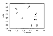
- Table 2 shows the results of B r and H cJ.
- 2A and 2B are schematic views for explaining a method for measuring the thickness of the first grain boundary.
- the thickness is 5 nm or more and 30 nm or less.
- the first grain boundaries (hereinafter sometimes referred to as "second grain boundaries") by the presence, without using Dy, R-T-B having a high B r and high H cJ It has been found that a sintered system magnet can be obtained.
- the composition and thickness of the first grain boundary (two-grain grain boundary) in the RTB-based sintered magnet have a great influence on the magnetization reversal behavior of the RTB-based sintered magnet.
- the thickness of the two-grain grain boundary is thin, the magnetic coupling between the crystal grains cannot be sufficiently broken, and it is expected that the magnetization reversal easily propagates beyond the crystal grains. It is difficult to obtain HcJ .
- As a means for thickening the two-particle grain boundary it is conceivable to secure a sufficient amount of liquid phase (grain boundary) in sintering and heat treatment.
- TEM The thickness of the two-grain grain boundary measured by a technique such as a transmission electron microscope is at most 5 nm, and it is difficult to increase the thickness further.
- the present inventors have recently found that a large amount of Fe exists in the grain boundary between two grains (for example, literature name: H. Sephri-Amin. Et.al, Acta Materia 60, P819 (2012).
- the physical properties of the two-grain boundary where a large amount of Fe exists are considered to be one of the reasons that the thickness of the two-grain boundary cannot be sufficiently increased.
- the present inventors have reduced the B content in the RTB-based sintered magnet from the stoichiometric ratio and contained Ga, so that the grain boundary is replaced with the R 2 T 17 phase.
- the Fe content in the grain boundary is reduced, and when no Cu is contained, the R phase or the R—Ga phase is used. When Cu is contained, the R phase is used. It was also found that the thickness of the two-grain grain boundary can be increased by forming the R—Ga phase and the R—Ga—Cu phase at the two-grain grain boundary.
- the R—T—Ga phase may have some magnetism.
- the R—T—Ga phase may cause magnetism.
- an increase in the thickness of the grain boundary is hindered.
- the amount of B is too low to generate the RT-Ga phase, the abundance ratio of the main phase is lowered, and high Br may not be obtained.
- an R phase, an R—Ga phase, an R phase, an R—Ga phase, and an R—Ga—Cu phase while suppressing the generation of an RT-Ga phase as much as possible at the two-grain grain boundary, The thickness of the two-particle grain boundary can be further increased, and HcJ can be improved.
- the generation of the R—T—Ga phase is excessively suppressed, the R phase, the R—Ga phase, the R phase, the R—Ga phase, and the R—Ga—Cu phase cannot be sufficiently generated.
- the amount of R 2 T 17 phase is adjusted by adjusting the R amount and the B amount within an appropriate range, and the Ga amount is optimized according to the amount of precipitation of the R 2 T 17 phase.
- the Ga amount is optimized according to the amount of precipitation of the R 2 T 17 phase.
- the “thickness of the first grain boundary (two grain grain boundary)” in the present invention is the thickness of the first grain boundary existing between the two main phases, and more specifically, among the grain boundaries. It means the maximum value of the thickness when the region with the largest thickness is measured. “The thickness of the first grain boundary (two-grain grain boundary)” is evaluated by the following procedure. 1) By scanning electron microscope (SEM) observation, five or more visual fields including a two-particle grain boundary having a length of 3 ⁇ m or more in the observation cross section are randomly selected. 2) For each field of view, after processing the sample so as to include the two-particle grain boundary phase by a microsampling method using a focused ion beam (FIB), until the thickness direction becomes 80 nm or less Process flakes.
- SEM scanning electron microscope
- FIB focused ion beam
- FIG. 2A is a diagram schematically illustrating an example of the first grain boundary
- FIG. 2B is an enlarged view of a portion surrounded by a dotted line in FIG.
- the first grain boundary 22 may include a region 24 having a large thickness and a region 26 having a small thickness.
- the maximum thickness of the region 24 having a large thickness is obtained.
- the value is the thickness of the first grain boundary 22.
- the second grain boundaries 32 existing between the first grain boundaries 22 and the three or more main phases 42 may be connected.
- the “thickness of the first grain boundary” refers to the vicinity of the boundary (from the first grain boundary 22 to the second grain boundary 32) that changes from the first grain boundary 22 to the second grain boundary 32 in the cross section of the magnet whose thickness is to be measured.
- the thickness of a region separated by about 0.5 ⁇ m from the boundaries 35 ⁇ / b> A and 35 ⁇ / b> B with the grain boundary 32 is not measured.
- the boundary is considered to be affected by the thickness of the second grain boundary 32.
- the range indicated by the braces denoted by reference numeral 22 in FIG. 2B indicates the range in which the first grain boundary 22 extends, and the measurement range of the thickness of the first grain boundary 22 is not necessarily limited. It should be noted that it does not indicate (that is, a range excluding a region separated by about 0.5 ⁇ m from the boundaries 35A and 35B).
- the present invention has a thickness it is possible to obtain a high B r and H cJ by the presence of a first grain boundary of 5nm or 30nm or less. If the thickness of the first grain boundary is less than 5 nm, the magnetic coupling between crystal grains cannot be sufficiently broken, and thus high HcJ cannot be obtained. It is possible to obtain a high H cJ exceeds 30nm, but reduces the abundance ratio of the main phase, there may not be obtained a high B r. Moreover, the preferable range of the thickness of the first grain boundary is 10 nm or more and 30 nm or less.
- composition of RTB-based sintered magnet is as follows.
- R 13.0 atomic% or more and 15 atomic% or less (R is Nd and / or Pr)
- B 5.2 atomic% or more and 5.6 atomic% or less
- Ga 0.2 atomic% or more and 1.0 atomic% or less
- Al 0.3 atomic% or less (including 0 atomic%)
- the balance consists of the balance T (T is Fe and 10% or less of Fe can be replaced by Co) and inevitable impurities.
- R 13.0 atomic% or more and 15 atomic% or less (R is Nd and / or Pr), B: 5.2 atomic% or more and 5.6 atomic% or less, Ga: 0.2 atomic% or more and 1.0 atomic% or less, Cu: 0.01 atomic% or more and 1.0 atomic% or less, Al: 0.3 atomic% or less (including 0 atomic%),
- T is Fe and 10% or less of Fe can be replaced by Co
- R amount, B quantity by combining such an extent that the Ga amount the respective, it is possible to obtain a high B r and high H cJ. If any of the R, B, and Ga amounts is out of the above range, the generation of the RTB Ga phase is too small, and the entire RTB system sintered magnet has an R phase and an R-Ga phase. Alternatively, the number of two-grain grain boundaries in which no R phase, R—Ga phase, and R—Ga—Cu phase are generated increases, and the thickness of the two-grain grain boundary does not increase. On the other hand, if too much RTB-Ga phase is generated at the grain boundary, in the entire RTB-based sintered magnet, the magnetism of RT-Ga phase prevents magnetic separation between crystal grains. Or an increase in the thickness of the grain boundary.
- R is Nd and / or Pr.
- the content of R is 13 atomic% or more and 15 atomic% or less.
- the content of B is set to 5.2 atomic% or more and 5.6 atomic% or less.
- the Ga content is 0.2 atom% or more and 1.0 atom% or less, preferably 0.4 atom% or more and 0.6 atom% or less.
- the balance T is Fe, and 10% or less of Fe can be replaced with Co. If the Co substitution amount exceeds 10%, Br is lowered, which is not preferable.
- Cu may be contained in an amount of 0.01 atomic% to 1.0 atomic%.
- an R—Ga—Cu phase is generated along with the R phase and the R—Ga phase at the two-grain grain boundary. From the generation of the R—Ga—Cu phase, HcJ is further improved as compared to the case of only the R—Ga phase.
- R—T—Ga phase means R: 15 mass% or more and 65 mass% or less (preferably R: 40 mass% or more and 65 mass% or less), T: 20 mass% or more and 80 mass% or less, Ga: 2% by mass or more and 20% by mass or less (R: 40% by mass or more and 65% by mass or less, T: 20% by mass or more and 55% by mass or less, Ga: 2% by mass or more and 15% by mass or less
- R—T—Ga phase may contain elements other than R, T, and Ga described above. As such other elements, for example, one or more elements selected from Al and Cu may be included.
- the R phase may contain 95% by mass or more of R, and examples thereof include Nd metal having a dhcp structure.
- the R—Ga phase may include R 70% by mass or more and 95% by mass or less, Ga 5% by mass or more and 30% by mass or less, and Fe 20% by mass or less (including 0), for example, R 3 Ga 1 compound. It is done.
- the R—Ga—Cu phase may be one in which a part of Ga in the R—Ga phase is substituted with Cu, and examples thereof include R 3 (Ga, Cu) 1 compounds.
- the R—Ga phase may form a phase with an Fe poor composition having other structures such as amorphous.
- the content of Fe or (Fe + Co) in the first grain boundary (double grain boundary) existing between the two main phases is preferably 20 atomic% or less (including 0 atomic%). This is because the thickness of the two-grain grain boundary can be increased by lowering the concentration of Fe or (Fe + Co) in the two-grain grain boundary. Furthermore, by lowering the concentration of (Fe + Co), the magnetic coupling between the main phases is broken, and there is an effect of improving HcJ .
- the Ga content is ⁇ Ga> / (1/17 ⁇ 100 ⁇ ⁇ B>) ( ⁇ Ga> is the Ga content expressed in atomic%).
- the atomic ratio is preferably 0.8 or more and 3.0 or less.
- the content of Ga and Cu is ⁇ Ga + Cu> / (1/17 ⁇ 100 ⁇ ⁇ B>) ( ⁇ Ga + Cu> is the total amount of Ga and Cu expressed in atomic%). Is preferably 1.0 or more and 3.0 or less in terms of the number of atoms.
- the amount of R and the amount of B are ⁇ B> / ⁇ R>( ⁇ R> is the amount of R expressed in atomic%) of 0.37 or more and 0.42 or less in terms of the number of atoms.
- H cJ can be further improved with further suppress a decrease in B r.
- the preferred composition of the RTB-based sintered magnet is as follows.
- R 13.0 atomic% or more and 15 atomic% or less (R is Nd and / or Pr)
- B 5.2 atomic% or more and 5.6 atomic% or less
- Ga 0.2 atomic% or more and 1.0 atomic% or less
- Al 0.69 atomic% or less (including 0 atomic%)
- T is a transition metal element and necessarily contains Fe
- R amount, B quantity, by a range such as the Ga amount, respectively it is possible to obtain a high B r and high H cJ. If any of the R amount, B amount, and Ga amount is out of the above range, the generation of the RT-Ga phase is too small or too large. If the R—T—Ga phase is too small, the R, R—Ga, R, R—Ga, and R—Ga—Cu phases are not generated in the entire RTB-based sintered magnet. The grain boundary increases and the thickness of the two grain boundary does not increase. On the other hand, if too much RTB-Ga phase is generated at the grain boundary, in the entire RTB-based sintered magnet, the magnetism of RT-Ga phase prevents magnetic separation between crystal grains. Or an increase in the thickness of the grain boundary.
- R is Nd and / or Pr.
- the content of R is 13 atomic% or more and 15 atomic% or less.
- the content of B is not less than 5.2 atom% and not more than 5.6 atom%, preferably not less than 5.2 atom% and not more than 5.43 atom%.
- the Ga content is 0.2 atom% or more and 1.0 atom% or less, preferably 0.4 atom% or more and 0.6 atom% or less.
- the balance T is a transition metal element and necessarily contains Fe. Examples of transition metal elements other than Fe include Co. However, if the substitution amount of Co exceeds 10%, Br is lowered, which is not preferable. Further, a small amount of V, Cr, Mn, Zr, Nb, Mo, Hf, Ta, W, or the like may be contained.
- an R—Ga—Cu phase is generated along with the R phase and the R—Ga phase at the two-grain grain boundary.
- HcJ is further improved as compared to the case of only the R—Ga phase.
- the Ga content is preferably in the range of the following formula (1). 0.8 ⁇ ⁇ Ga> / (1/17 ⁇ 100 ⁇ ⁇ B>) ⁇ 3.0 (1)
- ⁇ Ga> is the Ga amount expressed in atomic%
- ⁇ B> is the B amount expressed in atomic%.
- the Ga content falls within the range of the following formula (2). 1.03 ⁇ ⁇ Ga> / (1/17 ⁇ 100 ⁇ ⁇ B>) ⁇ 1.24 (2)
- ⁇ Ga> is the Ga amount expressed in atomic%
- ⁇ B> is the B amount expressed in atomic%.
- content of Ga and Cu is the range of following (3) Formula.
- ⁇ Ga + Cu> is the total amount of Ga and Cu expressed in atomic%
- ⁇ B> is the B amount expressed in atomic%
- the ratio of the number of atoms in the R amount and the B amount is preferably in the range of the following formula (4). 0.37 ⁇ ⁇ B> / ⁇ R> ⁇ 0.42 (4)
- ⁇ B> is the B amount expressed in atomic percent
- ⁇ R> is the R amount expressed in atomic percent.
- H cJ can be further improved with further suppress a decrease in B r.
- the manufacturing method of the RTB-based sintered magnet includes a process of obtaining alloy powder, a forming process, a sintering process, and a heat treatment process. Hereinafter, each step will be described.
- Step of obtaining alloy powder A metal or alloy of each element is prepared so as to have the above-described composition, and a flaky alloy is produced using the strip casting method or the like.
- the obtained flaky alloy is hydrogen crushed so that the size of the coarsely pulverized powder is 1.0 mm or less, for example.
- the coarsely pulverized powder is finely pulverized by a jet mill or the like, so that, for example, finely pulverized powder (alloy powder) having a particle diameter D50 (value obtained by a laser diffraction method by an air flow dispersion method (median diameter)) of 3 to 7 ⁇ m.
- a known lubricant may be used as an auxiliary agent for the coarsely pulverized powder before jet mill pulverization and the alloy powder during and after jet mill pulverization.
- Forming step Using the obtained alloy powder, forming in a magnetic field is performed to obtain a formed body.
- a dry alloy method in which a dry alloy powder is inserted into a mold cavity and molded while applying a magnetic field, a slurry in which the alloy powder is dispersed in the mold cavity is injected, Any known forming method in a magnetic field may be used, including a wet forming method of forming while discharging the slurry dispersion medium.
- a sintered magnet is obtained by sintering a molded object.
- a known method can be used for sintering the molded body.
- the atmosphere gas is preferably an inert gas such as helium or argon.
- the obtained sintered magnet may be subjected to machining such as grinding in order to adjust the magnet dimensions. In that case, the heat treatment may be performed before or after machining. Furthermore, you may surface-treat to the obtained sintered magnet.
- the surface treatment may be a known surface treatment, and for example, a surface treatment such as Al vapor deposition, electric Ni plating, or resin coating can be performed.
- the obtained coarsely pulverized powder was mixed with an airflow type pulverizer (jet mill device). Then, dry pulverization was performed in a nitrogen stream to obtain finely pulverized powder (alloy powder) having a particle diameter D50 (median diameter) of 4 ⁇ m. The oxygen concentration in the nitrogen gas during pulverization was controlled to 50 ppm or less.
- the particle size D50 is a value obtained by a laser diffraction method using an airflow dispersion method.
- the obtained alloy powder was mixed with a dispersion medium to prepare a slurry.
- Normaldodecane was used as a solvent, and methyl caprylate was mixed as a lubricant.
- the concentration of the slurry was 70% by mass of the alloy powder and 30% by mass of the dispersion medium, and the lubricant was 0.16% by mass with respect to 100% by mass of the alloy powder.
- the slurry was molded in a magnetic field to obtain a molded body.
- the magnetic field during molding was a static magnetic field of 0.8 MA / m, and the applied pressure was 5 MPa.
- molding apparatus transverse magnetic field shaping
- the obtained molded body was sintered in vacuum at 1020 ° C. for 4 hours to obtain a sintered magnet.
- the density of the sintered magnet was 7.5 Mg / m 3 or more.
- the obtained sintered body was held at 800 ° C. for 2 hours, then cooled to room temperature, then held at 500 ° C. for 2 hours and then cooled to room temperature, and then subjected to heat treatment. 1 to 11 RTB-based sintered magnets were produced.
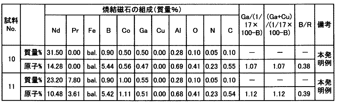
- Sample No. Tables 1 and 2 show the component analysis results (mass% and atomic%) of 1 to 11 and the measurement results of oxygen (O), nitrogen (N), and carbon (C). Further, ⁇ Ga> / (1/17 ⁇ 100) obtained from the atomic percentage when the amount of Fe is adjusted so that the whole is 100% by mass while ignoring impurities other than oxygen, nitrogen, and oxygen, and these results.
- - ⁇ B>) ⁇ Ga + Cu> / (1/17 ⁇ 100- ⁇ B>) and ⁇ B> / ⁇ R> values (all in atomic ratio) are shown in Tables 1 and 2.
- Sample No. After cutting the sintered magnets 1 to 11 by machining and polishing the cross section, SEM observation was performed, and the first grain boundary (two particles) existing between two main phases having a length of 3 ⁇ m or more in the observed cross section. 5 fields of view were randomly selected. For each field of view, a microsampling method using a focused ion beam (FIB) is used to include the first grain boundary selected, and the SEM observation plane has a thickness of 5 ⁇ m ⁇ width of 20 ⁇ m and a height of about 15 ⁇ m. After processing the sample so as to be a columnar shape, the sample was further processed into a thin piece until the thickness direction became 80 nm or less to prepare a sample for a transmission electron microscope (TEM).
- TEM transmission electron microscope
- the obtained sample was observed with a transmission electron microscope (TEM), and the thickness of the first grain boundary was measured. After confirming that the length of the two-grain boundary in the sample is 3 ⁇ m or more, exclude the region about 0.5 ⁇ m away from the vicinity of the boundary with the second grain boundary existing between three or more main phases. The thickness of the grain boundary in the region (the length was 2 ⁇ m or more) was evaluated, and the maximum value was defined as the thickness of the grain boundary phase. After determining the region where the thickness of the two-grain grain boundary is the largest, when measuring the maximum value of the thickness of the two-grain grain boundary, the measurement was performed with a high TEM magnification in order to accurately measure the thickness.
- TEM transmission electron microscope
- Table 3 shows the results of performing the same analysis on all five sampled first grain boundary phases and obtaining the average value.
- Sample No. By machining the sintered magnet of 1-11, vertical 7 mm, transverse 7 mm, to prepare a sample having a thickness of 7 mm, were measured B r and H cJ of the sample by B-H tracer. The obtained results are shown in Table 3.
- the sample No. of the present invention in which the thickness of the first grain boundary (two grain grain boundary) is 5 nm or more and 30 nm or less. 1-6 and 10, 11 are both high B r and high H cJ are achieved. Further, it was confirmed that particularly high HcJ was obtained in samples 3, 4, 5, 10, and 11 in which the thickness of the first grain boundary was 10 nm or more.
- the black rhombus plots 1 to 6, 10 and 11 in FIG. 1 to 6 and 10, 11, and white triangle plots 7 to 9 indicate the sample numbers of Comparative Examples. 7-9. As shown in FIG. 1, for example, sample No.
- the first grain boundary is a mixture of a thick region and a small region, as schematically shown in FIG. 2B, which is an enlarged schematic view of the cross section of the sintered magnet shown in FIG.
- the maximum value of the thickness of the thick region was defined as the thickness of the first grain boundary.
- the 1st grain boundary is evaluating the area
- sample no. 5 was subjected to Nd, Fe, Co, Cu, Ga, Al, O point analysis (beam diameter 2 nm) by energy dispersive X-ray spectroscopy (EDX).
- EDX energy dispersive X-ray spectroscopy
- the RTB-based sintered magnet according to the present invention can be suitably used for a hybrid vehicle or electric vehicle motor.
Landscapes
- Chemical & Material Sciences (AREA)
- Engineering & Computer Science (AREA)
- Materials Engineering (AREA)
- Mechanical Engineering (AREA)
- Metallurgy (AREA)
- Organic Chemistry (AREA)
- Power Engineering (AREA)
- Crystallography & Structural Chemistry (AREA)
- Inorganic Chemistry (AREA)
- Physics & Mathematics (AREA)
- Manufacturing & Machinery (AREA)
- Composite Materials (AREA)
- Electromagnetism (AREA)
- Hard Magnetic Materials (AREA)
- Powder Metallurgy (AREA)
Abstract
Description
R:13.0原子%以上15原子%以下(RはNdおよび/またはPr)、
B:5.2原子%以上5.6原子%以下、
Ga:0.2原子%以上1.0原子%以下、
Al:0.69原子%以下(0原子%を含む)、
残部がT(Tは遷移金属元素でありFeを必ず含む)および不可避的不純物からなることを特徴とする、R-T-B系焼結磁石である。
Cu:0.01原子%以上1.0原子%以下、
を更に含むことを特徴とする、R-T-B系焼結磁石である。
Al:0.3原子%以下(0原子%を含む)
であることを特徴とする、R-T-B系焼結磁石である。
B:5.2原子%以上5.43原子%以下
であることを特徴とする、R-T-B系焼結磁石である。
0.8≦<Ga>/(1/17×100-<B>)≦3.0 (1)
ここで<Ga>は原子%で表したGa量であり、<B>は原子%で表したB量である。
1.03≦<Ga>/(1/17×100-<B>)≦1.24 (2)
ここで<Ga>は原子%で表したGa量であり、<B>は原子%で表したB量である。
1.0≦<Ga+Cu>/(1/17×100-<B>)≦3.0 (3)
ここで<Ga+Cu>は原子%で表したGaとCuの合計量であり、<B>は原子%で表したB量である。
0.37≦<B>/<R>≦0.42 (4)
ここで<B>は原子%で表したB量であり、<R>は原子%で表したR量である。
1)走査電子顕微鏡(SEM)観察で、観察断面における長さが3μm以上ある二粒子粒界を含む視野をランダムに5視野以上選択する。
2)それぞれの視野に対して、収束イオンビーム(FIB)を用いたマイクロサンプリング法により、前記二粒子粒界相を含むように試料を加工した後、さらに、厚さ方向が80nm以下となるまで薄片加工する。
3)得られた薄片試料を透過電子顕微鏡(TEM)観察し、個々の二粒子粒界における最大値を求める。当然ながら、選択した前記二粒子粒界のうち厚みが最も大きい領域を決定した後、当該領域の厚みの最大値を測定する時は、精度良く測定するためにTEMの倍率を高めてもよい。
4)1)~3)の手順で観察したすべての二粒子粒界の平均値を求める。
図2(a)は、第一の粒界の例を模式的に示す図であり、図2(b)は、図2(a)の点線で囲んだ部分を拡大した図である。
図2(b)に示すように、第一の粒界22は厚みが大きい領域24と小さい領域26が混在している場合があるが、このような場合、厚みが大きい領域24の厚みの最大値を第一の粒界22の厚みとする。また、図2(b)に示すように、第一の粒界22と三つ以上の主相42間に存在する第二の粒界32はつながっている場合がある。この場合、「第一の粒界の厚み」とは、厚みを測定する磁石の断面において第一の粒界22から第二の粒界32にかわる境目近傍(第一の粒界22と第二の粒界32との境目35A、35Bから、0.5μm程度離れた領域)の厚みは測定しないこととする。前記境目は、第二の粒界32の厚みの影響をうけている可能性があると考えられるためである。ここで、図2(b)において符号22を付した中括弧が示す範囲は、第一の粒界22が延在する範囲を示すものであり、必ずしも第一の粒界22の厚みの測定範囲(すなわち、境目35A、35Bから0.5μm程度離れた領域を除いた範囲)を示すものではないことに留意されたい。
本発明の1つの実施形態に係るR-T-B系焼結磁石の好ましい組成は以下の通りである。
R:13.0原子%以上15原子%以下(RはNdおよび/またはPr)、
B:5.2原子%以上5.6原子%以下、
Ga:0.2原子%以上1.0原子%以下、
Al:0.3原子%以下(0原子%を含む)、
残部T(TはFeであり、Feの10%以下をCoで置換できる)および不可避的不純物からなる。
あるいは、
R:13.0原子%以上15原子%以下(RはNdおよび/またはPr)、
B:5.2原子%以上5.6原子%以下、
Ga:0.2原子%以上1.0原子%以下、
Cu:0.01原子%以上1.0原子%以下、
Al:0.3原子%以下(0原子%を含む)、
残部T(TはFeであり、Feの10%以下をCoで置換できる)および不可避的不純物からなる。
R:13.0原子%以上15原子%以下(RはNdおよび/またはPr)、
B:5.2原子%以上5.6原子%以下、
Ga:0.2原子%以上1.0原子%以下、
Al:0.69原子%以下(0原子%を含む)、
残部がT(Tは遷移金属元素でありFeを必ず含む)および不可避的不純物からなる。
0.8≦<Ga>/(1/17×100-<B>)≦3.0 (1)
ここで、<Ga>は原子%で表したGa量であり、<B>は原子%で表したB量である。
より好ましくは、Gaの含有量は下記(2)式の範囲となる。
1.03≦<Ga>/(1/17×100-<B>)≦1.24 (2)
ここで、<Ga>は原子%で表したGa量であり、<B>は原子%で表したB量である。
また、Cuを含有する場合は、GaとCuの含有量は、下記(3)式の範囲であることが好ましい。
1.0≦<Ga+Cu>/(1/17×100-<B>)≦3.0 (3)
ここで、<Ga+Cu>は原子%で表したGaとCuの合計量であり、<B>は原子%で表したB量である。
さらにR量、B量の原子数の比は、下記(4)式の範囲であることが好ましい。
0.37≦<B>/<R>≦0.42 (4)
ここで<B>は原子%で表したB量であり、<R>は原子%で表したR量である。
いずれの場合も、好ましい範囲にすることによって、Brの低下をより抑制するとともにHcJがより向上する。
R-T-B系焼結磁石の製造方法の一例を説明する。R-T-B系焼結磁石の製造方法は、合金粉末を得る工程、成形工程、焼結工程、熱処理工程を有する。以下、各工程について説明する。
前記組成となるようにそれぞれの元素の金属または合金を準備し、これらをストリップキャスティング法等を用いてフレーク状の合金を製造する。得られたフレーク状の合金を水素粉砕し、粗粉砕粉のサイズを例えば1.0mm以下とする。次に、粗粉砕粉をジェットミル等により微粉砕することで、例えば粒径D50(気流分散法によるレーザー回折法で得られた値(メジアン径))が3~7μmの微粉砕粉(合金粉末)を得る。なお、ジェットミル粉砕前の粗粉砕粉、ジェットミル粉砕中およびジェットミル粉砕後の合金粉末に助剤として公知の潤滑剤を使用してもよい。
得られた合金粉末を用いて磁界中成形を行い、成形体を得る。磁界中成形は、金型のキャビティー内に乾燥した合金粉末を挿入し、磁界を印加しながら成形する乾式成形法、金型のキャビティー内に該合金粉末を分散させたスラリーを注入し、スラリーの分散媒を排出しながら成形する湿式成形法を含む既知の任意の磁界中成形方法を用いてよい。
成形体を焼結することにより焼結磁石を得る。成形体の焼結は既知の方法を用いることができる。なお、焼結時の雰囲気による酸化を防止するために、焼結は、真空雰囲気中または雰囲気ガス中で行うことが好ましい。雰囲気ガスは、ヘリウム、アルゴンなどの不活性ガスを用いることが好ましい。
得られた焼結磁石に対し、磁気特性を向上させることを目的とした熱処理を行うことが好ましい。熱処理温度、熱処理時間などは公知の条件を採用することができる。得られた焼結磁石に磁石寸法の調整のため、研削などの機械加工を施してもよい。その場合、熱処理は機械加工前でも機械加工後でもよい。さらに、得られた焼結磁石に、表面処理を施してもよい。表面処理は、公知の表面処理で良く、例えばAl蒸着や電気Niめっきや樹脂塗装などの表面処理を行うことができる。

また、試料No.1~11の焼結磁石に機械加工を施して、縦7mm、横7mm、厚み7mmの試料を作製し、B-Hトレーサによって各試料のBr及びHcJを測定した。得られた結果を表3に示す。

24:厚みが大きい領域
26:厚みが小さい領域
30、32:第二の粒界
35A、35B:境目
40、42:主相
Claims (11)
- Nd2Fe14B型化合物を主相とし、前記主相と、二つの主相間に存在する第一の粒界と、三つ以上の主相間に存在する第二の粒界とを有するR-T-B系焼結磁石であって、厚みが5nm以上30nm以下の前記第一の粒界が存在していることを特徴とするR-T-B系焼結磁石。
- R-T-B系焼結磁石の組成が、
R:13.0原子%以上15原子%以下(RはNdおよび/またはPr)、
B:5.2原子%以上5.6原子%以下、
Ga:0.2原子%以上1.0原子%以下、
Al:0.69原子%以下(0原子%を含む)、
残部がT(Tは遷移金属元素でありFeを必ず含む)および不可避的不純物からなることを特徴とする請求項1に記載のR-T-B系焼結磁石。 - Cu:0.01原子%以上1.0原子%以下、
を更に含むことを特徴とする請求項2に記載のR-T-B系焼結磁石。 - Al:0.3原子%以下(0原子%を含む)
であることを特徴とする請求項2または3に記載のR-T-B系焼結磁石。 - B:5.2原子%以上5.43原子%以下
であることを特徴とする、請求項2~4のいずれか一項に記載のR-T-B系焼結磁石。 - 下記(1)式を満足することを特徴とする請求項2~5のいずれか一項に記載のR-T-B系焼結磁石。
0.8≦<Ga>/(1/17×100-<B>)≦3.0 (1)
ここで、<Ga>は原子%で表したGa量であり、<B>は原子%で表したB量である。 - 下記(2)式を満足することを特徴とする請求項6に記載のR-T-B系焼結磁石。
1.03≦<Ga>/(1/17×100-<B>)≦1.24 (2)
ここで、<Ga>は原子%で表したGa量であり、<B>は原子%で表したB量である。 - 下記(3)式を満足することを特徴とする請求項3または請求項3を引用する請求項4~7のいずれか一項に記載のR-T-B系焼結磁石。
1.0≦<Ga+Cu>/(1/17×100-<B>)≦3.0 (3)
ここで、<Ga+Cu>は原子%で表したGaとCuの合計量であり、<B>は原子%で表したB量である。 - 前記第一の粒界の厚みが10nm以上30nm以下であることを特徴とする請求項1~8のいずれか一項に記載のR-T-B系焼結磁石。
- B量とR量の原子数の比が、下記(4)式を満足することを特徴とする請求項2~9のいずれか一項に記載のR-T-B系焼結磁石。
0.37≦<B>/<R>≦0.42 (4)
ここで、<B>は原子%で表したB量であり、<R>は原子%で表したR量である。 - 前記第一の粒界のFeあるいは(Fe+Co)の含有量が20原子%以下(0原子%を含む)であることを特徴とする請求項2~10のいずれか一項に記載のR-T-B系焼結磁石。
Priority Applications (5)
| Application Number | Priority Date | Filing Date | Title |
|---|---|---|---|
| JP2015508652A JP6319299B2 (ja) | 2013-03-29 | 2014-03-27 | R−t−b系焼結磁石 |
| CN201480017376.1A CN105190793B (zh) | 2013-03-29 | 2014-03-27 | R-t-b系烧结磁体 |
| ES14776462.5T ES2674370T3 (es) | 2013-03-29 | 2014-03-27 | Imán sinterizado a base de R-T-B |
| US14/780,264 US20160042847A1 (en) | 2013-03-29 | 2014-03-27 | R-t-b based sintered magnet |
| EP14776462.5A EP2980808B1 (en) | 2013-03-29 | 2014-03-27 | R-t-b-based sintered magnet |
Applications Claiming Priority (2)
| Application Number | Priority Date | Filing Date | Title |
|---|---|---|---|
| JP2013-071833 | 2013-03-29 | ||
| JP2013071833 | 2013-03-29 |
Publications (1)
| Publication Number | Publication Date |
|---|---|
| WO2014157448A1 true WO2014157448A1 (ja) | 2014-10-02 |
Family
ID=51624410
Family Applications (1)
| Application Number | Title | Priority Date | Filing Date |
|---|---|---|---|
| PCT/JP2014/058737 Ceased WO2014157448A1 (ja) | 2013-03-29 | 2014-03-27 | R-t-b系焼結磁石 |
Country Status (6)
| Country | Link |
|---|---|
| US (1) | US20160042847A1 (ja) |
| EP (1) | EP2980808B1 (ja) |
| JP (1) | JP6319299B2 (ja) |
| CN (1) | CN105190793B (ja) |
| ES (1) | ES2674370T3 (ja) |
| WO (1) | WO2014157448A1 (ja) |
Cited By (21)
| Publication number | Priority date | Publication date | Assignee | Title |
|---|---|---|---|---|
| JP2014209546A (ja) * | 2013-03-28 | 2014-11-06 | Tdk株式会社 | 希土類磁石 |
| WO2015020183A1 (ja) * | 2013-08-09 | 2015-02-12 | Tdk株式会社 | R-t-b系焼結磁石、および、モータ |
| WO2015020182A1 (ja) * | 2013-08-09 | 2015-02-12 | Tdk株式会社 | R-t-b系焼結磁石、および、モータ |
| WO2016133067A1 (ja) * | 2015-02-17 | 2016-08-25 | 日立金属株式会社 | R-t-b系焼結磁石の製造方法 |
| EP3076408A1 (en) | 2015-03-31 | 2016-10-05 | Shin-Etsu Chemical Co., Ltd. | R-fe-b sintered magnet and making method |
| EP3076407A1 (en) | 2015-03-31 | 2016-10-05 | Shin-Etsu Chemical Co., Ltd. | R-fe-b sintered magnet and making method |
| EP3076406A1 (en) | 2015-03-31 | 2016-10-05 | Shin-Etsu Chemical Co., Ltd. | R-fe-b sintered magnet and making method |
| JPWO2015147053A1 (ja) * | 2014-03-26 | 2017-04-13 | 日立金属株式会社 | R−t−b系焼結磁石の製造方法 |
| EP3179487A1 (en) | 2015-11-18 | 2017-06-14 | Shin-Etsu Chemical Co., Ltd. | R-(fe,co)-b sintered magnet and making method |
| DE102017203073A1 (de) | 2016-02-26 | 2017-08-31 | Tdk Corporation | Permanentmagnet auf R-T-B Basis |
| DE102017203074A1 (de) | 2016-02-26 | 2017-08-31 | Tdk Corporation | Permanentmagnet auf R-T-B Basis |
| DE102017203059A1 (de) | 2016-02-26 | 2017-08-31 | Tdk Corporation | Permanentmagnet auf R-T-B Basis |
| EP3264429A1 (en) | 2016-06-20 | 2018-01-03 | Shin-Etsu Chemical Co., Ltd. | R-fe-b sintered magnet and making method |
| EP3309803A1 (en) | 2016-09-26 | 2018-04-18 | Shin-Etsu Chemical Co., Ltd. | Method for preparing r-fe-b sintered magnet |
| EP3309801A1 (en) | 2016-09-26 | 2018-04-18 | Shin-Etsu Chemical Co., Ltd. | R-fe-b sintered magnet |
| WO2018101239A1 (ja) | 2016-12-02 | 2018-06-07 | 信越化学工業株式会社 | R-Fe-B系焼結磁石及びその製造方法 |
| JP2018093201A (ja) * | 2016-12-06 | 2018-06-14 | Tdk株式会社 | R−t−b系永久磁石 |
| CN110024064A (zh) * | 2016-12-01 | 2019-07-16 | 日立金属株式会社 | R-t-b系烧结磁体及其制造方法 |
| JP2021034711A (ja) * | 2019-08-16 | 2021-03-01 | 包頭天和磁気材料科技股▲ふん▼有限公司 | 焼結体、焼結永久磁石およびそれらの製造方法 |
| DE112020001199T5 (de) | 2019-03-13 | 2021-11-25 | Tdk Corporation | Dauermagnet auf R-T-B-Basis und Verfahren zur Herstellung desselben |
| JP2022115921A (ja) * | 2016-12-06 | 2022-08-09 | Tdk株式会社 | R-t-b系永久磁石 |
Families Citing this family (11)
| Publication number | Priority date | Publication date | Assignee | Title |
|---|---|---|---|---|
| WO2014157451A1 (ja) * | 2013-03-29 | 2014-10-02 | 日立金属株式会社 | R-t-b系焼結磁石 |
| JP5999080B2 (ja) * | 2013-07-16 | 2016-09-28 | Tdk株式会社 | 希土類磁石 |
| JP6287167B2 (ja) * | 2013-07-16 | 2018-03-07 | Tdk株式会社 | 希土類磁石 |
| US10388442B2 (en) | 2013-08-12 | 2019-08-20 | Hitachi Metals, Ltd. | R-T-B based sintered magnet and method for producing R-T-B based sintered magnet |
| EP3038116B1 (en) * | 2013-08-12 | 2019-11-27 | Hitachi Metals, Ltd. | R-t-b system sintered magnet |
| CN105474337B (zh) | 2013-09-02 | 2017-12-08 | 日立金属株式会社 | R‑t‑b系烧结磁体的制造方法 |
| CN106448985A (zh) * | 2015-09-28 | 2017-02-22 | 厦门钨业股份有限公司 | 一种复合含有Pr和W的R‑Fe‑B系稀土烧结磁铁 |
| CN105609029B (zh) * | 2016-03-24 | 2019-10-01 | 深圳市华星光电技术有限公司 | 感测amoled像素驱动特性的系统及amoled显示装置 |
| US10529473B2 (en) * | 2016-03-28 | 2020-01-07 | Tdk Corporation | R-T-B based permanent magnet |
| JP6992634B2 (ja) * | 2018-03-22 | 2022-02-03 | Tdk株式会社 | R-t-b系永久磁石 |
| JP7293772B2 (ja) * | 2019-03-20 | 2023-06-20 | Tdk株式会社 | R-t-b系永久磁石 |
Citations (2)
| Publication number | Priority date | Publication date | Assignee | Title |
|---|---|---|---|---|
| JP2011082365A (ja) * | 2009-10-07 | 2011-04-21 | Hitachi Metals Ltd | R−t−b系焼結磁石 |
| WO2013008756A1 (ja) | 2011-07-08 | 2013-01-17 | 昭和電工株式会社 | R-t-b系希土類焼結磁石用合金、r-t-b系希土類焼結磁石用合金の製造方法、r-t-b系希土類焼結磁石用合金材料、r-t-b系希土類焼結磁石、r-t-b系希土類焼結磁石の製造方法およびモーター |
Family Cites Families (8)
| Publication number | Priority date | Publication date | Assignee | Title |
|---|---|---|---|---|
| US8128759B2 (en) * | 2006-12-21 | 2012-03-06 | Ulvac, Inc. | Permanent magnet and method of manufacturing same |
| JP2009231391A (ja) * | 2008-03-19 | 2009-10-08 | Hitachi Metals Ltd | R−t−b系焼結磁石 |
| JP5303738B2 (ja) * | 2010-07-27 | 2013-10-02 | Tdk株式会社 | 希土類焼結磁石 |
| KR101243347B1 (ko) * | 2011-01-25 | 2013-03-13 | 한양대학교 산학협력단 | 기계적 물성이 향상된 R-Fe-B계 소결자석 및 이의 제조방법 |
| WO2012102497A2 (en) * | 2011-01-25 | 2012-08-02 | Industry-University Cooperation Foundation, Hanyang University | R-fe-b sintered magnet with enhanced mechanical properties and method for producing the same |
| JP5948033B2 (ja) * | 2011-09-21 | 2016-07-06 | 株式会社日立製作所 | 焼結磁石 |
| JP6303480B2 (ja) * | 2013-03-28 | 2018-04-04 | Tdk株式会社 | 希土類磁石 |
| WO2014157451A1 (ja) * | 2013-03-29 | 2014-10-02 | 日立金属株式会社 | R-t-b系焼結磁石 |
-
2014
- 2014-03-27 JP JP2015508652A patent/JP6319299B2/ja active Active
- 2014-03-27 CN CN201480017376.1A patent/CN105190793B/zh active Active
- 2014-03-27 EP EP14776462.5A patent/EP2980808B1/en active Active
- 2014-03-27 WO PCT/JP2014/058737 patent/WO2014157448A1/ja not_active Ceased
- 2014-03-27 ES ES14776462.5T patent/ES2674370T3/es active Active
- 2014-03-27 US US14/780,264 patent/US20160042847A1/en not_active Abandoned
Patent Citations (2)
| Publication number | Priority date | Publication date | Assignee | Title |
|---|---|---|---|---|
| JP2011082365A (ja) * | 2009-10-07 | 2011-04-21 | Hitachi Metals Ltd | R−t−b系焼結磁石 |
| WO2013008756A1 (ja) | 2011-07-08 | 2013-01-17 | 昭和電工株式会社 | R-t-b系希土類焼結磁石用合金、r-t-b系希土類焼結磁石用合金の製造方法、r-t-b系希土類焼結磁石用合金材料、r-t-b系希土類焼結磁石、r-t-b系希土類焼結磁石の製造方法およびモーター |
Non-Patent Citations (1)
| Title |
|---|
| H. SEPEHRI-AMIN, ACTA MATERIALIA, vol. 60, 2012, pages 819 |
Cited By (44)
| Publication number | Priority date | Publication date | Assignee | Title |
|---|---|---|---|---|
| JP2014209546A (ja) * | 2013-03-28 | 2014-11-06 | Tdk株式会社 | 希土類磁石 |
| JPWO2015020183A1 (ja) * | 2013-08-09 | 2017-03-02 | Tdk株式会社 | R−t−b系焼結磁石、および、モータ |
| WO2015020183A1 (ja) * | 2013-08-09 | 2015-02-12 | Tdk株式会社 | R-t-b系焼結磁石、および、モータ |
| WO2015020182A1 (ja) * | 2013-08-09 | 2015-02-12 | Tdk株式会社 | R-t-b系焼結磁石、および、モータ |
| US10109403B2 (en) | 2013-08-09 | 2018-10-23 | Tdk Corporation | R-T-B based sintered magnet and motor |
| US10388441B2 (en) | 2013-08-09 | 2019-08-20 | Tdk Corporation | R-T-B based sintered magnet and motor |
| JPWO2015020182A1 (ja) * | 2013-08-09 | 2017-03-02 | Tdk株式会社 | R−t−b系焼結磁石、および、モータ |
| JPWO2015147053A1 (ja) * | 2014-03-26 | 2017-04-13 | 日立金属株式会社 | R−t−b系焼結磁石の製造方法 |
| WO2016133067A1 (ja) * | 2015-02-17 | 2016-08-25 | 日立金属株式会社 | R-t-b系焼結磁石の製造方法 |
| JPWO2016133067A1 (ja) * | 2015-02-17 | 2017-11-30 | 日立金属株式会社 | R−t−b系焼結磁石の製造方法 |
| EP3076407A1 (en) | 2015-03-31 | 2016-10-05 | Shin-Etsu Chemical Co., Ltd. | R-fe-b sintered magnet and making method |
| KR20160117365A (ko) | 2015-03-31 | 2016-10-10 | 신에쓰 가가꾸 고교 가부시끼가이샤 | R―Fe―B계 소결 자석 및 그의 제조 방법 |
| KR20160117364A (ko) | 2015-03-31 | 2016-10-10 | 신에쓰 가가꾸 고교 가부시끼가이샤 | R―Fe―B계 소결 자석 및 그의 제조 방법 |
| US10515747B2 (en) | 2015-03-31 | 2019-12-24 | Shin-Etsu Chemical Co., Ltd. | R-Fe-B sintered magnet and making method |
| US10410775B2 (en) | 2015-03-31 | 2019-09-10 | Shin-Etsu Chemical Co., Ltd. | R—Fe—B sintered magnet and making method |
| KR20160117363A (ko) | 2015-03-31 | 2016-10-10 | 신에쓰 가가꾸 고교 가부시끼가이샤 | R―Fe―B계 소결 자석 및 그의 제조 방법 |
| EP3076406A1 (en) | 2015-03-31 | 2016-10-05 | Shin-Etsu Chemical Co., Ltd. | R-fe-b sintered magnet and making method |
| EP3076408A1 (en) | 2015-03-31 | 2016-10-05 | Shin-Etsu Chemical Co., Ltd. | R-fe-b sintered magnet and making method |
| US9892831B2 (en) | 2015-03-31 | 2018-02-13 | Shin-Etsu Chemical Co., Ltd. | R-Fe—B sintered magnet and making method |
| EP3179487A1 (en) | 2015-11-18 | 2017-06-14 | Shin-Etsu Chemical Co., Ltd. | R-(fe,co)-b sintered magnet and making method |
| US10573438B2 (en) | 2015-11-18 | 2020-02-25 | Shin-Etsu Chemical Co., Ltd. | R-(Fe, Co)-B sintered magnet and making method |
| DE102017203073A1 (de) | 2016-02-26 | 2017-08-31 | Tdk Corporation | Permanentmagnet auf R-T-B Basis |
| US10943717B2 (en) | 2016-02-26 | 2021-03-09 | Tdk Corporation | R-T-B based permanent magnet |
| US10784028B2 (en) | 2016-02-26 | 2020-09-22 | Tdk Corporation | R-T-B based permanent magnet |
| US10672546B2 (en) | 2016-02-26 | 2020-06-02 | Tdk Corporation | R-T-B based permanent magnet |
| JP2017157833A (ja) * | 2016-02-26 | 2017-09-07 | Tdk株式会社 | R−t−b系永久磁石 |
| DE102017203059A1 (de) | 2016-02-26 | 2017-08-31 | Tdk Corporation | Permanentmagnet auf R-T-B Basis |
| DE102017203074A1 (de) | 2016-02-26 | 2017-08-31 | Tdk Corporation | Permanentmagnet auf R-T-B Basis |
| US11315710B2 (en) | 2016-06-20 | 2022-04-26 | Shin-Etsu Chemical Co., Ltd. | R-Fe-B sintered magnet and making method |
| EP3264429A1 (en) | 2016-06-20 | 2018-01-03 | Shin-Etsu Chemical Co., Ltd. | R-fe-b sintered magnet and making method |
| EP3309801A1 (en) | 2016-09-26 | 2018-04-18 | Shin-Etsu Chemical Co., Ltd. | R-fe-b sintered magnet |
| US10937578B2 (en) | 2016-09-26 | 2021-03-02 | Shin-Etsu Chemical Co., Ltd. | Method for preparing R—Fe—B sintered magnet |
| EP3309803A1 (en) | 2016-09-26 | 2018-04-18 | Shin-Etsu Chemical Co., Ltd. | Method for preparing r-fe-b sintered magnet |
| CN110024064B (zh) * | 2016-12-01 | 2020-03-03 | 日立金属株式会社 | R-t-b系烧结磁体及其制造方法 |
| CN110024064A (zh) * | 2016-12-01 | 2019-07-16 | 日立金属株式会社 | R-t-b系烧结磁体及其制造方法 |
| US10916373B2 (en) * | 2016-12-01 | 2021-02-09 | Hitachi Metals, Ltd. | R-T-B sintered magnet and production method therefor |
| US20190326053A1 (en) * | 2016-12-01 | 2019-10-24 | Hitachi Metals, Ltd. | R-t-b sintered magnet and production method therefor |
| KR20190091289A (ko) | 2016-12-02 | 2019-08-05 | 신에쓰 가가꾸 고교 가부시끼가이샤 | R-Fe-B계 소결 자석 및 그 제조 방법 |
| US11600413B2 (en) | 2016-12-02 | 2023-03-07 | Shin-Etsu Chemical Co., Ltd. | R—Fe—B sintered magnet and production method therefor |
| WO2018101239A1 (ja) | 2016-12-02 | 2018-06-07 | 信越化学工業株式会社 | R-Fe-B系焼結磁石及びその製造方法 |
| JP2022115921A (ja) * | 2016-12-06 | 2022-08-09 | Tdk株式会社 | R-t-b系永久磁石 |
| JP2018093201A (ja) * | 2016-12-06 | 2018-06-14 | Tdk株式会社 | R−t−b系永久磁石 |
| DE112020001199T5 (de) | 2019-03-13 | 2021-11-25 | Tdk Corporation | Dauermagnet auf R-T-B-Basis und Verfahren zur Herstellung desselben |
| JP2021034711A (ja) * | 2019-08-16 | 2021-03-01 | 包頭天和磁気材料科技股▲ふん▼有限公司 | 焼結体、焼結永久磁石およびそれらの製造方法 |
Also Published As
| Publication number | Publication date |
|---|---|
| JP6319299B2 (ja) | 2018-05-09 |
| JPWO2014157448A1 (ja) | 2017-02-16 |
| EP2980808A4 (en) | 2016-12-14 |
| EP2980808A1 (en) | 2016-02-03 |
| CN105190793A (zh) | 2015-12-23 |
| US20160042847A1 (en) | 2016-02-11 |
| CN105190793B (zh) | 2018-07-24 |
| ES2674370T3 (es) | 2018-06-29 |
| EP2980808B1 (en) | 2018-06-13 |
Similar Documents
| Publication | Publication Date | Title |
|---|---|---|
| JP6319299B2 (ja) | R−t−b系焼結磁石 | |
| JP6288076B2 (ja) | R−t−b系焼結磁石 | |
| JP6501038B2 (ja) | R−t−b系焼結磁石 | |
| JP6414654B1 (ja) | R−t−b系焼結磁石の製造方法 | |
| CN105453194B (zh) | R-t-b系烧结磁体 | |
| JP6090550B1 (ja) | R−t−b系焼結磁石およびその製造方法 | |
| CN106030736B (zh) | R-t-b系烧结磁体的制造方法 | |
| WO2015022946A1 (ja) | R-t-b系焼結磁石およびr-t-b系焼結磁石の製造方法 | |
| JP6094612B2 (ja) | R−t−b系焼結磁石の製造方法 | |
| JP6798546B2 (ja) | R−t−b系焼結磁石の製造方法 | |
| WO2019181249A1 (ja) | R-t-b系焼結磁石の製造方法 | |
| JP2018028123A (ja) | R−t−b系焼結磁石の製造方法 | |
| WO2016153056A1 (ja) | 希土類磁石 | |
| JP2015135935A (ja) | 希土類磁石 | |
| JP6541038B2 (ja) | R−t−b系焼結磁石 | |
| JP2016164958A (ja) | R−t−b系焼結磁石 | |
| JPWO2019065481A1 (ja) | R−t−b系焼結磁石の製造方法 | |
| JP6474043B2 (ja) | R−t−b系焼結磁石 | |
| JP2018125445A (ja) | R−t−b系焼結磁石 | |
| JP6623998B2 (ja) | R−t−b系焼結磁石の製造方法 | |
| JP6610957B2 (ja) | R−t−b系焼結磁石の製造方法 | |
| CN111755189B (zh) | R-t-b系烧结磁体的制造方法 | |
| JP2019169698A (ja) | R−t−b系焼結磁石の製造方法 | |
| JP6229938B2 (ja) | R−t−b系焼結磁石 | |
| JP2018060997A (ja) | R−t−b系焼結磁石の製造方法 |
Legal Events
| Date | Code | Title | Description |
|---|---|---|---|
| WWE | Wipo information: entry into national phase |
Ref document number: 201480017376.1 Country of ref document: CN |
|
| 121 | Ep: the epo has been informed by wipo that ep was designated in this application |
Ref document number: 14776462 Country of ref document: EP Kind code of ref document: A1 |
|
| ENP | Entry into the national phase |
Ref document number: 2015508652 Country of ref document: JP Kind code of ref document: A |
|
| WWE | Wipo information: entry into national phase |
Ref document number: 2014776462 Country of ref document: EP |
|
| WWE | Wipo information: entry into national phase |
Ref document number: 14780264 Country of ref document: US |
|
| NENP | Non-entry into the national phase |
Ref country code: DE |