WO2014155619A1 - 半導体装置、電力変換装置および半導体装置の製造方法 - Google Patents
半導体装置、電力変換装置および半導体装置の製造方法 Download PDFInfo
- Publication number
- WO2014155619A1 WO2014155619A1 PCT/JP2013/059323 JP2013059323W WO2014155619A1 WO 2014155619 A1 WO2014155619 A1 WO 2014155619A1 JP 2013059323 W JP2013059323 W JP 2013059323W WO 2014155619 A1 WO2014155619 A1 WO 2014155619A1
- Authority
- WO
- WIPO (PCT)
- Prior art keywords
- bonding layer
- semiconductor device
- layer
- conductive member
- semiconductor
- Prior art date
- Legal status (The legal status is an assumption and is not a legal conclusion. Google has not performed a legal analysis and makes no representation as to the accuracy of the status listed.)
- Ceased
Links
Images






Classifications
-
- H—ELECTRICITY
- H10—SEMICONDUCTOR DEVICES; ELECTRIC SOLID-STATE DEVICES NOT OTHERWISE PROVIDED FOR
- H10W—GENERIC PACKAGES, INTERCONNECTIONS, CONNECTORS OR OTHER CONSTRUCTIONAL DETAILS OF DEVICES COVERED BY CLASS H10
- H10W72/00—Interconnections or connectors in packages
- H10W72/90—Bond pads, in general
-
- H—ELECTRICITY
- H10—SEMICONDUCTOR DEVICES; ELECTRIC SOLID-STATE DEVICES NOT OTHERWISE PROVIDED FOR
- H10W—GENERIC PACKAGES, INTERCONNECTIONS, CONNECTORS OR OTHER CONSTRUCTIONAL DETAILS OF DEVICES COVERED BY CLASS H10
- H10W72/00—Interconnections or connectors in packages
- H10W72/01—Manufacture or treatment
- H10W72/019—Manufacture or treatment of bond pads
- H10W72/01931—Manufacture or treatment of bond pads using blanket deposition
-
- H—ELECTRICITY
- H10—SEMICONDUCTOR DEVICES; ELECTRIC SOLID-STATE DEVICES NOT OTHERWISE PROVIDED FOR
- H10W—GENERIC PACKAGES, INTERCONNECTIONS, CONNECTORS OR OTHER CONSTRUCTIONAL DETAILS OF DEVICES COVERED BY CLASS H10
- H10W72/00—Interconnections or connectors in packages
- H10W72/071—Connecting or disconnecting
- H10W72/073—Connecting or disconnecting of die-attach connectors
-
- H—ELECTRICITY
- H10—SEMICONDUCTOR DEVICES; ELECTRIC SOLID-STATE DEVICES NOT OTHERWISE PROVIDED FOR
- H10W—GENERIC PACKAGES, INTERCONNECTIONS, CONNECTORS OR OTHER CONSTRUCTIONAL DETAILS OF DEVICES COVERED BY CLASS H10
- H10W72/00—Interconnections or connectors in packages
- H10W72/071—Connecting or disconnecting
- H10W72/073—Connecting or disconnecting of die-attach connectors
- H10W72/07331—Connecting techniques
-
- H—ELECTRICITY
- H10—SEMICONDUCTOR DEVICES; ELECTRIC SOLID-STATE DEVICES NOT OTHERWISE PROVIDED FOR
- H10W—GENERIC PACKAGES, INTERCONNECTIONS, CONNECTORS OR OTHER CONSTRUCTIONAL DETAILS OF DEVICES COVERED BY CLASS H10
- H10W72/00—Interconnections or connectors in packages
- H10W72/071—Connecting or disconnecting
- H10W72/073—Connecting or disconnecting of die-attach connectors
- H10W72/07351—Connecting or disconnecting of die-attach connectors characterised by changes in properties of the die-attach connectors during connecting
- H10W72/07352—Connecting or disconnecting of die-attach connectors characterised by changes in properties of the die-attach connectors during connecting changes in structures or sizes
-
- H—ELECTRICITY
- H10—SEMICONDUCTOR DEVICES; ELECTRIC SOLID-STATE DEVICES NOT OTHERWISE PROVIDED FOR
- H10W—GENERIC PACKAGES, INTERCONNECTIONS, CONNECTORS OR OTHER CONSTRUCTIONAL DETAILS OF DEVICES COVERED BY CLASS H10
- H10W72/00—Interconnections or connectors in packages
- H10W72/30—Die-attach connectors
- H10W72/321—Structures or relative sizes of die-attach connectors
-
- H—ELECTRICITY
- H10—SEMICONDUCTOR DEVICES; ELECTRIC SOLID-STATE DEVICES NOT OTHERWISE PROVIDED FOR
- H10W—GENERIC PACKAGES, INTERCONNECTIONS, CONNECTORS OR OTHER CONSTRUCTIONAL DETAILS OF DEVICES COVERED BY CLASS H10
- H10W72/00—Interconnections or connectors in packages
- H10W72/30—Die-attach connectors
- H10W72/321—Structures or relative sizes of die-attach connectors
- H10W72/325—Die-attach connectors having a filler embedded in a matrix
-
- H—ELECTRICITY
- H10—SEMICONDUCTOR DEVICES; ELECTRIC SOLID-STATE DEVICES NOT OTHERWISE PROVIDED FOR
- H10W—GENERIC PACKAGES, INTERCONNECTIONS, CONNECTORS OR OTHER CONSTRUCTIONAL DETAILS OF DEVICES COVERED BY CLASS H10
- H10W72/00—Interconnections or connectors in packages
- H10W72/30—Die-attach connectors
- H10W72/351—Materials of die-attach connectors
- H10W72/352—Materials of die-attach connectors comprising metals or metalloids, e.g. solders
-
- H—ELECTRICITY
- H10—SEMICONDUCTOR DEVICES; ELECTRIC SOLID-STATE DEVICES NOT OTHERWISE PROVIDED FOR
- H10W—GENERIC PACKAGES, INTERCONNECTIONS, CONNECTORS OR OTHER CONSTRUCTIONAL DETAILS OF DEVICES COVERED BY CLASS H10
- H10W72/00—Interconnections or connectors in packages
- H10W72/50—Bond wires
- H10W72/59—Bond pads specially adapted therefor
-
- H—ELECTRICITY
- H10—SEMICONDUCTOR DEVICES; ELECTRIC SOLID-STATE DEVICES NOT OTHERWISE PROVIDED FOR
- H10W—GENERIC PACKAGES, INTERCONNECTIONS, CONNECTORS OR OTHER CONSTRUCTIONAL DETAILS OF DEVICES COVERED BY CLASS H10
- H10W72/00—Interconnections or connectors in packages
- H10W72/90—Bond pads, in general
- H10W72/931—Shapes of bond pads
Definitions
- the present invention relates to a semiconductor device, a power conversion device, and a method for manufacturing a semiconductor device.
- a substrate having a conductive pattern, a semiconductor element disposed on the conductive pattern of the substrate, and a conductive pattern and the semiconductor element disposed between the conductive pattern of the substrate and the semiconductor element.
- a semiconductor device including a bonding layer for bonding the two is disclosed.
- the bonding layer of this semiconductor device includes a three-layered sintered pattern in the longitudinal section. Of the three-layered sintered pattern, the uppermost layer sintered pattern is bonded to the entire back surface of the semiconductor element, and the lowermost layer sintered pattern is bonded to the conductive pattern of the substrate.
- the uppermost layer of the three-layered sintered patterns constituting the bonding layer is bonded to the entire surface including the inner side of the back surface of the semiconductor element and the vicinity of the outer peripheral portion. Therefore, when the porosity of the uppermost layer sintering pattern is large, the bonding force between particles is weak, so when thermal stress is applied, the uppermost layer sintering pattern peels off or sinters. There is a problem that cracks (cracks) may occur in the pattern.
- the present invention has been made in order to solve the above-described problems, and one object of the present invention is to bond the component to the component while suppressing the peeling of the bonding layer and the occurrence of cracks in the vicinity of the outer peripheral portion of the component.
- a semiconductor device a power conversion device, and a method for manufacturing a semiconductor device capable of suppressing the destruction of components when a thermal stress is applied due to a difference in thermal expansion coefficient from the layer It is.
- a semiconductor device is disposed between a conductive member, a semiconductor device component disposed on the conductive member, and the conductive member and the semiconductor device component, and joins the conductive member and the semiconductor device component.
- the bonding layer includes a first bonding layer disposed on the inner side of the outer edge of the semiconductor device component in a plan view, and disposed on the outer side of the first bonding layer, than the first bonding layer. And a second bonding layer having a small porosity.
- the first bonding layer disposed on the inner side of the outer edge of the semiconductor device component, and the void disposed on the outer side of the first bonding layer and smaller than the first bonding layer.
- the thermal expansion coefficient difference between the semiconductor device component and the bonding layer can be reduced.
- the thermal stress is alleviated by the first bonding layer having a large porosity, so that the semiconductor device component can be prevented from being broken.
- the part is destroyed when thermal stress is applied due to the difference in coefficient of thermal expansion between the part and the joining layer, while suppressing the peeling and cracking of the joining layer near the outer periphery of the part. Can be suppressed.
- a power conversion device is disposed between a conductive member, a power conversion device component disposed on the conductive member, and the conductive member and the power conversion device component.
- a joining layer that joins the component, and the joining layer is disposed on the inner side of the outer edge of the component for the power conversion device in a plan view, disposed on the outer side of the first joining layer, And a second bonding layer having a smaller porosity than the one bonding layer.
- the first bonding layer disposed on the inner side of the outer edge of the power converter device component, and disposed on the outer side of the first bonding layer, than the first bonding layer.
- the inside of the power converter device component is bonded by the first bonding layer having a larger porosity than the second bonding layer.
- the thermal stress is applied, the thermal stress is relaxed by the first bonding layer having a large porosity, so that it is possible to suppress the destruction of the power converter device component.
- the part is destroyed when thermal stress is applied due to the difference in coefficient of thermal expansion between the part and the joining layer, while suppressing the peeling and cracking of the joining layer near the outer periphery of the part. It is possible to provide a power conversion device that can suppress this.
- a method for manufacturing a semiconductor device includes a step of forming a first metal paste layer on a conductive member, a step of arranging a component for a semiconductor device so as to cover the first metal paste layer, and a first metal paste layer Forming a first bonding layer for bonding the conductive member and the semiconductor device component by heat treatment, and a metal having an average particle size smaller than the first metal paste layer in the vicinity of the end of the semiconductor device component.
- the step of forming the second metal paste layer containing particles and the heat treatment of the second metal paste layer joins the conductive member and the vicinity of the end of the semiconductor device component, and the gap is smaller than the first bonding layer. Forming a second bonding layer having a rate.
- a step of bonding the conductive member and the vicinity of the end of the semiconductor device component and forming a second bonding layer having a smaller porosity than the first bonding layer is provided.
- the outside of the semiconductor device component is bonded by the second bonding layer having a smaller porosity than the first bonding layer. Therefore, the semiconductor device is formed by the second bonding layer having a small void ratio in which the bonding force between particles is strong. The peeling of the bonding layer and the occurrence of cracks (cracks) in the vicinity of the outer peripheral portion of the parts for use can be suppressed.
- the thermal expansion coefficient difference between the semiconductor device component and the bonding layer can be reduced.
- the thermal stress is alleviated by the first bonding layer having a large porosity, so that the semiconductor device component can be prevented from being broken.
- the part is destroyed when thermal stress is applied due to the difference in coefficient of thermal expansion between the part and the joining layer, while suppressing the peeling and cracking of the joining layer near the outer periphery of the part. It is possible to provide a method for manufacturing a semiconductor device capable of suppressing this.
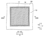
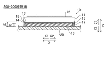
- FIG. 3 is a cross-sectional view taken along line 200-200 in FIG. It is the SEM image which showed an example of the joining layer of the three-phase inverter apparatus by one Embodiment. It is sectional drawing for demonstrating the process of forming a pattern electrode in the semiconductor wafer by one Embodiment. It is sectional drawing for demonstrating the process of forming a substantially V-shaped groove part in the semiconductor wafer by one Embodiment. It is sectional drawing for demonstrating the process of forming a metal layer in the semiconductor wafer by one Embodiment.
- the power modules 100a to 100c and the three-phase inverter device 100 are examples of “semiconductor device” and “power conversion device”.
- the three-phase inverter device 100 is configured by electrically connecting three power modules 100a, 100b, and 100c that respectively perform U-phase, V-phase, and W-phase power conversion. ing.
- Power modules 100a, 100b, and 100c each convert DC power input from DC power supply (not shown) through input terminals P and N into AC power of three phases (U phase, V phase, and W phase). Is configured to do.
- the power modules 100a, 100b, and 100c are configured to output the U-phase, V-phase, and W-phase AC power converted as described above to the outside via the output terminals U, V, and W, respectively. ing.
- the output terminals U, V, and W are connected to a motor (not shown).
- the power module 100a includes two semiconductor switch elements 1a and 2a.
- the semiconductor switch element 1a (2a) has three electrodes (gate electrode G1a (G2a), source electrode S1a (S2a), and drain electrode D1a (D2a)).
- the semiconductor switch elements 1a and 2a are composed of, for example, a SiC device, a GaN device, a Si device (MOSFET (field effect transistor), IGBT (insulated gate bipolar transistor), or bipolar transistor)). Yes.
- the semiconductor switch elements 1a and 2a are examples of “semiconductor device components”, “semiconductor elements”, and “power converter device components”.
- Semiconductor switching elements 1a and 2a perform switching based on a control signal input from the outside via control terminals 3a and 4a, respectively, so that the DC power input via input terminals P and N is converted to U phase. It is comprised so that it may convert into the alternating current power of this, and it may output outside via the output terminal U.
- the drain electrode D1a of the semiconductor switch element 1a is connected to the input terminal P, and the gate electrode G1a is connected to the control terminal 3a.
- the source electrode S1a of the semiconductor switch element 1a is connected to the output terminal U and the drain electrode D2a of the semiconductor switch element 2a.
- the drain electrode D2a of the semiconductor switch element 2a is connected to the output terminal U, and the gate electrode G2a is connected to the control terminal 4a.
- the source electrode S2a of the semiconductor switch element 2a is connected to the input terminal N.
- the power module 100b includes two semiconductor switch elements 1b and 2b.
- the semiconductor switch element 1b (2b) has three electrodes (a gate electrode G1b (G2b), a source electrode S1b (S2b), and a drain electrode D1b (D2b)).
- the semiconductor switch elements 1b and 2b are examples of “semiconductor device components”, “semiconductor elements”, and “power converter device components”.
- the semiconductor switch elements 1b and 2b perform switching on the basis of a control signal input from the outside via the control terminals 3b and 4b, respectively, so that the DC power input via the input terminals P and N is supplied to the V-phase. It is comprised so that it may convert into the alternating current power of this, and it may output outside via the output terminal V.
- the power module 100c also includes two semiconductor switch elements 1c and 2c.
- the semiconductor switch element 1c (2c) has three electrodes (a gate electrode G1c (G2c), a source electrode S1c (S2c), and a drain electrode D1c (D2c)).
- the semiconductor switch elements 1 c and 2 c are examples of “semiconductor device components”, “semiconductor elements”, and “power converter device components”.
- the semiconductor switch elements 1c and 2c perform switching on the basis of a control signal input from the outside via the control terminals 3c and 4c, respectively, so that the DC power input via the input terminals P and N is supplied to the W phase. It is comprised so that it may convert into the alternating current power of this, and it may output outside via the output terminal W.
- the semiconductor element 10 is a component for a power converter including the semiconductor switch elements 1a and 2a (1b and 2b, 1c and 2c) of the power module 100a (100b and 100c).
- the semiconductor element 10 is an example of a “semiconductor device component” and a “power converter device component”.
- the semiconductor element 10 is disposed on the conductive member 20.
- the semiconductor element 10 and the conductive member 20 are bonded by a bonding layer (a first bonding layer 16 and a second bonding layer 17) disposed between the semiconductor element 10 and the conductive member 20.
- the conductive member 20 may be provided as a conductive pattern on a substrate (not shown), or may be provided as a terminal electrode or a bonding electrode on an electronic component (not shown).
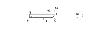
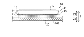
- the semiconductor element 10 is formed in a substantially rectangular shape in plan view (viewed from the Z direction). As shown in FIG. 3, the semiconductor element 10 includes an element portion 11, a terminal electrode 12, a bonding electrode 13, a metal layer 14, and a chamfered portion 15.
- the element part 11 is comprised by the semiconductor material containing SiC, GaN, Si, etc., for example.
- the terminal electrode 12 is provided on the upper surface (surface on the Z2 direction side) of the element portion 11.
- the terminal electrode 12 includes, for example, a drain electrode, a source electrode, or a gate electrode.
- the bonding electrode 13 is provided on the lower surface (the surface on the Z1 direction side) of the element portion 11.
- the bonding electrode 13 is provided for bonding to the conductive member 20 via the metal layer 14.
- the metal layer 14 is formed on the surface of the chamfered portion 15 and the surface on the conductive member 20 side (Z1 direction side) other than the chamfered portion 15. That is, the metal layer 14 is formed so as to cover the lower surface (surface on the Z1 direction side) of the bonding electrode 13 and the surface of the chamfered portion 15. Further, the metal layer 14 is provided in order to join the conductive member 20.
- the chamfered portion 15 is provided at the end of the element portion 11 (semiconductor element 10) on the conductive member 20 side (Z1 direction side). Specifically, the chamfered portion 15 is provided in a circumferential shape along four sides including four corners on the conductive member 20 side (Z1 direction side) of the substantially rectangular semiconductor element 10. Further, the chamfered portion 15 has an oblique flat surface having a predetermined angle with respect to the lower surface (the surface on the Z1 direction side) of the element portion 11.
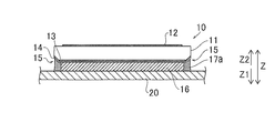
- the bonding layer for bonding the semiconductor element 10 and the conductive member 20 includes the first bonding layer 16 and the second bonding layer 17. .
- the first bonding layer 16 is disposed on the inner side of the outer edge of the semiconductor element 10 in a plan view (viewed from the Z direction).
- the second bonding layer 17 is disposed outside the first bonding layer 16. Further, the second bonding layer 17 is disposed in the vicinity of the end portion of the semiconductor element 10 in plan view.
- the first bonding layer 16 is disposed inside the chamfered portion 15 of the semiconductor element 10.
- the second bonding layer 17 is disposed so as to be connected (bonded) to both the first bonding layer 16 disposed inside the chamfered portion 15 and the chamfered portion 15.
- the first bonding layer 16 is connected (bonded) to the surface on the conductive member 20 side (Z1 direction side) other than the chamfered portion 15 of the semiconductor element 10 via the metal layer 14.
- the second bonding layer 17 is connected (bonded) to the chamfered portion 15 of the semiconductor element 10 through the metal layer 14.
- the planar area of the second bonding layer 17 is smaller than the planar area of the first bonding layer 16 in plan view.
- the maximum thickness h ⁇ b> 2 of the second bonding layer 17 is larger than the maximum thickness h ⁇ b> 1 of the first bonding layer 16. That is, since the second bonding layer 17 is connected (bonded) to the chamfered portion 15, the maximum thickness is correspondingly increased.
- the second bonding layer 17 is connected (bonded) to the semiconductor element 10 in a circumferential shape along four sides including the four corners of the substantially rectangular semiconductor element 10. .
- the porosity of the second bonding layer 17 is smaller than the porosity of the first bonding layer 16. That is, the first bonding layer 16 is in a porous state (with a high porosity), and the second bonding layer 17 is in a dense state (with a low porosity). Specifically, the porosity of the first bonding layer 16 is 10% or more and 30% or less, and the porosity of the second bonding layer 17 is 1% or less.
- the porosity of the bonding layer is, for example, as shown in FIG. 4, from the SEM (scanning electron microscope) image, the area of the metal portion appearing white and the area of the void portion appearing black per unit area of the SEM image. And is obtained by calculation.
- the first bonding layer 16 and the second bonding layer 17 are formed of a metal material containing the same metal. Specifically, the first bonding layer 16 and the second bonding layer 17 are each formed of a metal material mainly containing Ag.
- the second bonding layer 17 is formed of a metal material including metal particles having an average particle size smaller than the average particle size of metal particles included in the metal material forming the first bonding layer 16.
- the first bonding layer 16 is formed of a metal material mainly including Ag particles having a submicron (for example, 100 nm to 600 nm) size.
- the second bonding layer 17 is mainly formed of a metal material containing Ag particles having a size of 50 nm or less.
- the step of forming semiconductor element 10 In the method for manufacturing three-phase inverter device 100 (power modules 100a, 100b and 100c), the step of forming semiconductor element 10, the step of forming first metal paste layer 16a on conductive member 20, and the semiconductor element 10 are arranged.
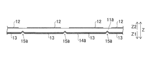
- the step of forming the semiconductor element 10 includes a step of forming the terminal electrode 12 and the electrode layer 13a on the semiconductor wafer 11a, a step of forming a groove portion 15a having a substantially V-shaped cross section on one surface of the semiconductor wafer 11a, It includes a step of forming the metal layer 14a so as to cover one surface of the semiconductor wafer 11a including the groove portion 15a, and a step of dicing the semiconductor wafer 11a.
- a plurality of terminal electrodes 12 corresponding to the semiconductor element 10 are provided on the upper surface (the surface on the Z2 direction side) of the semiconductor wafer 11a. It is formed.
- an electrode layer 13a is formed on the lower surface (surface on the Z1 direction side) of the semiconductor wafer 11a.
- the groove 15a having a substantially V-shaped cross section on one surface of the semiconductor wafer 11a As shown in FIG. 6, a lower surface (surface on the Z1 direction side) of the semiconductor wafer 11a is used with a V-shaped dicing blade. As a result of the half-cutting, the groove 15a is formed in the semiconductor wafer 11a.
- the electrode layer 13a is divided by the groove 15a to form a plurality of bonding electrodes 13.
- the metal layer 14a is formed on the lower surface (surface in the Z1 direction) of the semiconductor wafer 11a by sputtering. Is formed.
- the metal layer 14a is formed so as to cover the groove 15a and the bonding electrode 13 on the lower surface (the surface on the Z1 direction side) of the semiconductor wafer 11a.
- the semiconductor wafer 11a is divided (diced) along the groove 15a, so that the chamfer 15 is provided at the end and the chamfer 15 is provided.
- a plurality of semiconductor elements 10 (see FIG. 9) having the metal layer 14 covering the surface on the side (Z1 direction side) are formed.
- the first metal paste layer 16a is formed on the surface of the conductive member 20 on the Z2 side so as to be smaller than the plane area of the semiconductor element 10. 16a is applied.
- the first metal paste layer 16a is formed of a paste-like material in which metal particles mainly composed of submicron-sized Ag particles are dispersed in an organic solvent.
- the semiconductor element 10 is arranged on the Z2 direction side so as to cover the first metal paste layer 16a.
- the first bonding layer 16 that bonds the conductive member 20 and the semiconductor element 10 is formed by heat-treating the first metal paste layer 16a. . For example, by heating at 200 ° C. for 1 hour, the organic solvent is vaporized and removed from the first metal paste layer 16a, and the first bonding layer 16 made of metal (Ag) is formed.
- the step of forming the second metal paste layer 17a in the step of forming the second metal paste layer 17a, as shown in FIG. 13, metal particles having an average particle size smaller than that of the first metal paste layer 16a in the vicinity of the end of the semiconductor element 10 A second metal paste layer 17a containing is formed.
- a paste-like material is supplied between the semiconductor element 10 and the conductive member 20 by a dispense nozzle (not shown) to form the second metal paste layer 17a.
- the second metal paste layer 17a is formed of a paste-like material in which metal particles mainly composed of nano-sized Ag particles are dispersed in an organic solvent.
- the second metal paste layer 17a is heat-treated to bond the conductive member 20 and the vicinity of the end of the semiconductor element 10 as shown in FIG.
- a second bonding layer 17 having a smaller porosity than the layer 16 is formed. For example, by heating at 200 ° C. for 1 hour, the organic solvent is vaporized and removed from the second metal paste layer 17a, and the second bonding layer 17 made of metal (Ag) is formed.
- the first bonding layer 16 disposed on the inner side of the outer edge of the semiconductor element 10 and the outer side of the first bonding layer 16 in plan view (viewed from the Z direction).
- the outside is bonded by the second bonding layer 17 having a smaller porosity than the first bonding layer 16. Therefore, peeling and cracking (cracking) of the bonding layer in the vicinity of the outer peripheral portion of the semiconductor element 10 can be suppressed by the second bonding layer having a small porosity with a strong bonding force between particles.
- the thermal stress is relaxed by the first bonding layer 16 having a large porosity, so that the semiconductor element 10 can be prevented from being destroyed.
- the thermal stress is applied due to the difference in coefficient of thermal expansion between the semiconductor element 10 and the bonding layer, the peeling and cracking of the bonding layer in the vicinity of the outer peripheral portion of the semiconductor element 10 are suppressed. It can suppress that 10 is destroyed.
- the second bonding layer 17 is connected to the vicinity of the end of the semiconductor element 10, so that the vicinity of the end of the semiconductor element 10 where the thermal stress is concentrated is changed to the first bonding layer. Since the second bonding layer 17 having a porosity smaller than 16 can be connected, peeling and cracking (cracking) of the bonding layer in the vicinity of the outer peripheral portion of the semiconductor element 10 can be effectively suppressed.
- the first bonding layer 16 and the second bonding layer 17 are formed of a metal material containing the same metal as the first bonding layer 16 and the second bonding layer 17. Since it can suppress that the difference of a thermal expansion coefficient becomes large, it can suppress that the 1st joining layer 16 and the 2nd joining layer 17 peel.
- the second bonding layer 17 and the semiconductor element are connected by connecting the second bonding layer 17 to the chamfered portion 15 of the semiconductor element 10 as compared with the case where the chamfered portion 15 is not provided. 10 can be increased, so that the bonding strength between the conductive member 20 and the semiconductor element 10 by the second bonding layer 17 can be improved.
- the first bonding layer 16 is disposed on the inner side of the chamfered portion 15 of the semiconductor element 10 in plan view (viewed from the Z direction), and the second bonding layer 17 is formed.
- the first bonding layer 16 disposed inside the chamfered portion 15 and the chamfered portion 15 are both connected.
- the second bonding layer 17 having a small porosity can be disposed without any gap with respect to the first bonding layer 16, so that peeling and cracks (cracks) of the first bonding layer 16 are effectively suppressed. be able to.
- the first bonding layer 16 is connected to the surface on the conductive member 20 side (Z1 direction side) other than the chamfered portion 15 of the semiconductor element 10 via the metal layer 14.
- the second bonding layer 17 is connected to the chamfered portion 15 of the semiconductor element 10 through the metal layer 14.
- the maximum thickness h2 of the second bonding layer 17 is made larger than the maximum thickness h1 of the first bonding layer 16, so that the second bonding layer 17 having a small porosity is obtained.
- the connection area between the second bonding layer 17 and the semiconductor element 10 can be increased.
- the bonding strength between the conductive member 20 and the semiconductor element 10 by the second bonding layer 17 can be improved.
- the semiconductor element 10 is formed in a substantially rectangular shape in plan view (viewed from the Z direction), and the second bonding layer 17 is formed in the substantially rectangular semiconductor element 10. Connect to the four corners. Accordingly, the four corners of the substantially rectangular semiconductor element 10 where the thermal stress is most concentrated can be connected by the second bonding layer 17 having a small porosity, so that the bonding layer near the outer peripheral portion of the semiconductor element 10 can be connected. Peeling and cracking can be effectively suppressed.
- the chamfered portions 15 are provided circumferentially along the four sides of the surface of the substantially rectangular semiconductor element 10 on the conductive member 20 side (Z1 direction side), and the second bonding is performed.
- the layers 17 are connected circumferentially along the four sides of the substantially rectangular semiconductor element 10.
- the second bonding layer 17 and the semiconductor element 10 are connected circumferentially along the substantially rectangular four sides, and the bonding strength between the conductive member 20 and the semiconductor element 10 by the second bonding layer 17 is easy. Can be improved.
- the planar area of the second bonding layer 17 is made smaller than the planar area of the first bonding layer 16 in plan view (as viewed from the Z direction).
- the planar area of the second bonding layer 17 is made smaller than the planar area of the first bonding layer 16 in plan view (as viewed from the Z direction).
- the first bonding layer 16 and the second bonding layer 17 are each formed of a metal material containing Ag, thereby improving the heat resistance and bonding strength of the bonding layer. Can do.
- the porosity of the first bonding layer 16 is set to 10% or more and 30% or less, and the porosity of the second bonding layer 17 is set to 1% or less.
- the semiconductor element 10 is destroyed when a thermal stress is applied due to the difference in thermal expansion coefficient between the semiconductor element 10 and the bonding layer while ensuring the bonding strength between the semiconductor element 10 and the bonding layer. It can suppress more reliably.
- the second bonding layer 17 includes metal particles having an average particle size smaller than the average particle size of the metal particles included in the metal material forming the first bonding layer 16. It is made of a metal material. Thereby, the porosity of the second bonding layer 17 can be easily made smaller than the porosity of the first bonding layer 16.
- a three-phase inverter device is shown as an example of the power conversion device, but a power conversion device other than the three-phase inverter device may be used.
- a three-phase inverter device is shown as an example of the semiconductor device, but a semiconductor device other than the three-phase inverter device may be used.
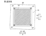
- the 2nd joining layer showed the structure connected circumferentially along 4 sides of the components for semiconductor devices (semiconductor element) of substantially rectangular shape
- the second bonding layer 27 may be connected to at least four corners of a substantially rectangular semiconductor device component (semiconductor element).
- the chamfered portion of the semiconductor device component only needs to be provided in at least four corners.
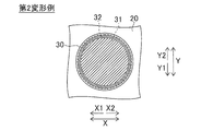
- the semiconductor device component and the power conversion device component may be components such as the columnar electrode 30 disposed on the conductive member 20.
- the conductive member 20 and the columnar electrode 30 are the first bonding layer 31 and the second bonding layer 32 that is disposed outside the first bonding layer 31 and has a smaller porosity than the first bonding layer 31. You may join.
- the 1st joining layer and the 2nd joining layer showed the structure formed of the metal material containing Ag
- the 1st joining layer and the 2nd joining layer are Au, Ag, or What is necessary is just to be formed with the metal material containing at least 1 among Cu.
- the chamfered part of the component for semiconductor devices showed the example formed so that it might have an inclined flat surface which has a predetermined angle with respect to the lower surface of a semiconductor element
- the chamfered portion may be an R chamfer having a curved surface.
- the porosity of the 1st joining layer was 10% or more and 30% or less, the example of the structure whose porosity of a 2nd joining layer is 1% or less was shown, If the porosity is smaller than the porosity of the first bonding layer, the porosity of the first bonding layer and the porosity of the second bonding layer may be other ratios.
- the process of forming a semiconductor element although the process of forming a semiconductor element showed the structure containing the process of forming the electrode layer 13a, the process of forming a semiconductor element does not include the process of forming the electrode layer 13a. Good. In this case, after forming the groove portion, the metal layer 14a is formed so as to cover one surface of the semiconductor wafer including the groove portion, so that the metal layer 14a forms the electrode layer 13a even if the electrode layer 13a is not formed in advance. I will also serve.
Landscapes
- Inverter Devices (AREA)
- Die Bonding (AREA)
Abstract
Description
10 半導体素子(半導体装置用部品、電力変換装置用部品)
14 金属層
15 面取り部
16、31 第1接合層(接合層)
16a 第1金属ペースト層
17、27、32 第2接合層(接合層)
17a 第2金属ペースト層
20 導電部材
30 柱状電極(半導体装置用部品、電力変換装置用部品)
100 3相インバータ装置(半導体装置、電力変換装置)
100a、100b、100c パワーモジュール(半導体装置、電力変換装置)
Claims (18)
- 導電部材(20)と、
前記導電部材上に配置される半導体装置用部品(1a~1c、2a~2c、10、30)と、
前記導電部材と前記半導体装置用部品との間に配置され、前記導電部材と前記半導体装置用部品とを接合する接合層とを備え、
前記接合層は、
平面視において、前記半導体装置用部品の外縁よりも内側に配置された第1接合層(16、31)と、
前記第1接合層の外側に配置され、前記第1接合層よりも小さい空隙率を有する第2接合層(17、27、32)とを含む、半導体装置。 - 前記第2接合層は、前記半導体装置用部品の端部近傍に接続している、請求項1に記載の半導体装置。
- 前記第1接合層および前記第2接合層は、互いに同じ金属を含む金属材料により形成されている、請求項1または2に記載の半導体装置。
- 前記半導体装置用部品は、前記導電部材側の面の端部に設けられた面取り部(15)を含み、
前記第2接合層は、前記半導体装置用部品の前記面取り部に接続している、請求項1~3のいずれか1項に記載の半導体装置。 - 前記第1接合層は、平面視において、前記半導体装置用部品の面取り部よりも内側に配置されており、
前記第2接合層は、前記面取り部の内側に配置された前記第1接合層と、前記面取り部との両方に接続している、請求項4に記載の半導体装置。 - 前記半導体装置用部品は、半導体素子(1a~1c、2a~2c、10)を含むとともに、前記半導体素子の前記面取り部の表面および前記面取り部以外の前記導電部材側の表面に形成された金属層(14)を含み、
前記第1接合層は、前記金属層を介して前記半導体素子の前記面取り部以外の前記導電部材側の表面に接続されており、
前記第2接合層は、前記金属層を介して前記半導体素子の前記面取り部に接続されている、請求項4または5に記載の半導体装置。 - 前記第2接合層の最大厚みは、前記第1接合層の最大厚みよりも大きい、請求項4~6のいずれか1項に記載の半導体装置。
- 前記半導体装置用部品は、平面視において、略矩形形状に形成されており、
前記第2接合層は、略矩形形状の前記半導体装置用部品の少なくとも4隅に接続されている、請求項1~7のいずれか1項に記載の半導体装置。 - 前記略矩形形状の半導体装置用部品は、前記導電部材側の面の少なくとも4隅に設けられた面取り部を含む、請求項8に記載の半導体装置。
- 前記第2接合層は、前記略矩形形状の半導体装置用部品の4辺に沿って周状に接続されている、請求項8または9に記載の半導体装置。
- 平面視において、前記第2接合層の平面積は、前記第1接合層の平面積よりも小さい、請求項1~10のいずれか1項に記載の半導体装置。
- 前記第1接合層および前記第2接合層は、それぞれ、Au、AgまたはCuのうち少なくとも1つを含む金属材料により形成されている、請求項1~11のいずれか1項に記載の半導体装置。
- 前記第1接合層の空隙率は、10%以上30%以下であり、
前記第2接合層の空隙率は、1%以下である、請求項1~12のいずれか1項に記載の半導体装置。 - 前記第2接合層は、前記第1接合層を形成する金属材料に含まれる金属粒子の平均粒径よりも小さい平均粒径を有する金属粒子を含む金属材料により形成されている、請求項1~13のいずれか1項に記載の半導体装置。
- 導電部材(20)と、
前記導電部材上に配置される電力変換装置用部品(1a~1c、2a~2c、10、30)と、
前記導電部材と前記電力変換装置用部品との間に配置され、前記導電部材と前記電力変換装置用部品とを接合する接合層とを備え、
前記接合層は、
平面視において、前記電力変換装置用部品の外縁よりも内側に配置された第1接合層(16、31)と、
前記第1接合層の外側に配置され、前記第1接合層よりも小さい空隙率を有する第2接合層(17、27、32)とを含む、電力変換装置。 - 導電部材(20)に第1金属ペースト層(16a)を形成する工程と、
前記第1金属ペースト層を覆うように半導体装置用部品(1a~1c、2a~2c、10、30)を配置する工程と、
前記第1金属ペースト層を熱処理することにより、前記導電部材と前記半導体装置用部品とを接合する第1接合層(16、31)を形成する工程と、
前記半導体装置用部品の端部近傍に前記第1金属ペースト層よりも小さい平均粒径を有する金属粒子を含む第2金属ペースト層(17a)を形成する工程と、
前記第2金属ペースト層を熱処理することにより、前記導電部材と前記半導体装置用部品の端部近傍とを接合するとともに、前記第1接合層よりも小さい空隙率を有する第2接合層(17、27、32)を形成する工程とを備える、半導体装置の製造方法。 - 前記半導体装置用部品の前記導電部材側の面の端部に面取り部(15)を形成する工程をさらに備え、
前記第2接合層を形成する工程は、前記半導体装置用部品の前記面取り部に前記第2接合層が接続するように形成する工程を含む、請求項16に記載の半導体装置の製造方法。 - 前記第2接合層を形成する工程は、略矩形形状の前記半導体装置用部品の少なくとも4隅に前記第2接合層が接続するように形成する工程を含む、請求項16または17に記載の半導体装置の製造方法。
Priority Applications (3)
| Application Number | Priority Date | Filing Date | Title |
|---|---|---|---|
| PCT/JP2013/059323 WO2014155619A1 (ja) | 2013-03-28 | 2013-03-28 | 半導体装置、電力変換装置および半導体装置の製造方法 |
| JP2015507815A JPWO2014155619A1 (ja) | 2013-03-28 | 2013-03-28 | 半導体装置、電力変換装置および半導体装置の製造方法 |
| CN201380074724.4A CN105190856A (zh) | 2013-03-28 | 2013-03-28 | 半导体装置、电力转换装置和半导体装置的制造方法 |
Applications Claiming Priority (1)
| Application Number | Priority Date | Filing Date | Title |
|---|---|---|---|
| PCT/JP2013/059323 WO2014155619A1 (ja) | 2013-03-28 | 2013-03-28 | 半導体装置、電力変換装置および半導体装置の製造方法 |
Publications (1)
| Publication Number | Publication Date |
|---|---|
| WO2014155619A1 true WO2014155619A1 (ja) | 2014-10-02 |
Family
ID=51622692
Family Applications (1)
| Application Number | Title | Priority Date | Filing Date |
|---|---|---|---|
| PCT/JP2013/059323 Ceased WO2014155619A1 (ja) | 2013-03-28 | 2013-03-28 | 半導体装置、電力変換装置および半導体装置の製造方法 |
Country Status (3)
| Country | Link |
|---|---|
| JP (1) | JPWO2014155619A1 (ja) |
| CN (1) | CN105190856A (ja) |
| WO (1) | WO2014155619A1 (ja) |
Cited By (6)
| Publication number | Priority date | Publication date | Assignee | Title |
|---|---|---|---|---|
| JP2015216160A (ja) * | 2014-05-08 | 2015-12-03 | 三菱電機株式会社 | 電力用半導体装置および電力用半導体装置の製造方法 |
| JP2016100424A (ja) * | 2014-11-20 | 2016-05-30 | 三菱電機株式会社 | パワーモジュール |
| JPWO2018037992A1 (ja) * | 2016-08-22 | 2018-08-23 | 千住金属工業株式会社 | 金属焼結接合体、およびダイ接合方法 |
| JP2019029662A (ja) * | 2017-08-02 | 2019-02-21 | ローム株式会社 | 半導体装置および半導体装置の製造方法 |
| WO2020026516A1 (ja) * | 2018-07-30 | 2020-02-06 | 株式会社日立製作所 | 半導体装置、焼結金属シートおよび焼結金属シートの製造方法 |
| US11626352B2 (en) | 2017-08-02 | 2023-04-11 | Rohm Co., Ltd. | Semiconductor device and method for manufacturing the same |
Citations (3)
| Publication number | Priority date | Publication date | Assignee | Title |
|---|---|---|---|---|
| JPH06177178A (ja) * | 1992-12-01 | 1994-06-24 | Nissan Motor Co Ltd | 半導体チップの構造 |
| JP2008085097A (ja) * | 2006-09-28 | 2008-04-10 | Kyocera Corp | 半田ボールおよびその製造方法 |
| JP2011165871A (ja) * | 2010-02-09 | 2011-08-25 | Denso Corp | 電子装置およびその製造方法 |
Family Cites Families (1)
| Publication number | Priority date | Publication date | Assignee | Title |
|---|---|---|---|---|
| JP4758869B2 (ja) * | 2006-11-08 | 2011-08-31 | 新光電気工業株式会社 | 半導体装置の製造方法 |
-
2013
- 2013-03-28 CN CN201380074724.4A patent/CN105190856A/zh active Pending
- 2013-03-28 WO PCT/JP2013/059323 patent/WO2014155619A1/ja not_active Ceased
- 2013-03-28 JP JP2015507815A patent/JPWO2014155619A1/ja active Pending
Patent Citations (3)
| Publication number | Priority date | Publication date | Assignee | Title |
|---|---|---|---|---|
| JPH06177178A (ja) * | 1992-12-01 | 1994-06-24 | Nissan Motor Co Ltd | 半導体チップの構造 |
| JP2008085097A (ja) * | 2006-09-28 | 2008-04-10 | Kyocera Corp | 半田ボールおよびその製造方法 |
| JP2011165871A (ja) * | 2010-02-09 | 2011-08-25 | Denso Corp | 電子装置およびその製造方法 |
Cited By (13)
| Publication number | Priority date | Publication date | Assignee | Title |
|---|---|---|---|---|
| JP2015216160A (ja) * | 2014-05-08 | 2015-12-03 | 三菱電機株式会社 | 電力用半導体装置および電力用半導体装置の製造方法 |
| JP2016100424A (ja) * | 2014-11-20 | 2016-05-30 | 三菱電機株式会社 | パワーモジュール |
| EP3489991A4 (en) * | 2016-08-22 | 2020-10-21 | Senju Metal Industry Co., Ltd | METAL Sintered Bonding Body and Chip Bonding Method |
| JPWO2018037992A1 (ja) * | 2016-08-22 | 2018-08-23 | 千住金属工業株式会社 | 金属焼結接合体、およびダイ接合方法 |
| US11024598B2 (en) | 2016-08-22 | 2021-06-01 | Senju Metal Industry Co., Ltd. | Metallic sintered bonding body and die bonding method |
| JP2019029662A (ja) * | 2017-08-02 | 2019-02-21 | ローム株式会社 | 半導体装置および半導体装置の製造方法 |
| JP7149751B2 (ja) | 2017-08-02 | 2022-10-07 | ローム株式会社 | 半導体装置 |
| US11626352B2 (en) | 2017-08-02 | 2023-04-11 | Rohm Co., Ltd. | Semiconductor device and method for manufacturing the same |
| US12288739B2 (en) | 2017-08-02 | 2025-04-29 | Rohm Co., Ltd. | Semiconductor device and method for manufacturing the same |
| JP2020021756A (ja) * | 2018-07-30 | 2020-02-06 | 株式会社日立製作所 | 半導体装置、焼結金属シートおよび焼結金属シートの製造方法 |
| WO2020026516A1 (ja) * | 2018-07-30 | 2020-02-06 | 株式会社日立製作所 | 半導体装置、焼結金属シートおよび焼結金属シートの製造方法 |
| JP7072462B2 (ja) | 2018-07-30 | 2022-05-20 | 株式会社日立製作所 | 半導体装置、焼結金属シートおよび焼結金属シートの製造方法 |
| US11437338B2 (en) | 2018-07-30 | 2022-09-06 | Hitachi, Ltd. | Semiconductor device, sintered metal sheet, and method for manufacturing sintered metal sheet |
Also Published As
| Publication number | Publication date |
|---|---|
| CN105190856A (zh) | 2015-12-23 |
| JPWO2014155619A1 (ja) | 2017-02-16 |
Similar Documents
| Publication | Publication Date | Title |
|---|---|---|
| WO2014155619A1 (ja) | 半導体装置、電力変換装置および半導体装置の製造方法 | |
| CN105612690B (zh) | 半导体装置 | |
| CN110622301A (zh) | 功率半导体装置及其制造方法 | |
| JP6726112B2 (ja) | 半導体装置および電力変換装置 | |
| JP6196853B2 (ja) | 3レベルコンバータハーフブリッジ | |
| JP6169250B2 (ja) | 電力用半導体装置 | |
| CN110235244A (zh) | 功率半导体模块以及电力转换装置 | |
| CN104124877A (zh) | 三级变流器半桥 | |
| JP6154104B2 (ja) | 少なくとも一つの電子部品を、第1および第2端子の間のループインダクタンスを低減する手段を含む電力供給装置に電気的に相互接続するための装置 | |
| CN105931954A (zh) | 半导体装置、半导体装置的制造方法以及电力变换装置 | |
| JP2018190930A (ja) | パワー半導体モジュール及びその製造方法並びに電力変換装置 | |
| JP2014022579A (ja) | パワーモジュール半導体装置 | |
| JP6906611B2 (ja) | 半導体素子接合用基板、半導体装置および電力変換装置 | |
| WO2016103335A1 (ja) | 半導体装置およびそれを用いた電力変換装置 | |
| CN114846598A (zh) | 功率模块和电力变换装置 | |
| WO2017159081A1 (ja) | 半導体モジュール | |
| JP2014120638A (ja) | パワーモジュール半導体装置およびその製造方法 | |
| US11107760B2 (en) | Semiconductor device, electric power conversion apparatus and method for manufacturing semiconductor device | |
| JP2014053403A (ja) | パワーモジュール半導体装置 | |
| JP2018107481A (ja) | パワーモジュール半導体装置 | |
| JP2019102535A (ja) | 半導体モジュール、その製造方法及び電力変換装置 | |
| JPWO2019171523A1 (ja) | 半導体素子、半導体装置、電力変換装置、及び、半導体素子の製造方法 | |
| WO2016071982A1 (ja) | 半導体モジュールおよび半導体モジュール用の導電部材 | |
| JP2020043154A (ja) | 半導体装置及びその製造方法、並びに、電力変換装置 | |
| WO2018066496A1 (ja) | パワーモジュールおよび電力変換装置 |
Legal Events
| Date | Code | Title | Description |
|---|---|---|---|
| WWE | Wipo information: entry into national phase |
Ref document number: 201380074724.4 Country of ref document: CN |
|
| 121 | Ep: the epo has been informed by wipo that ep was designated in this application |
Ref document number: 13879823 Country of ref document: EP Kind code of ref document: A1 |
|
| ENP | Entry into the national phase |
Ref document number: 2015507815 Country of ref document: JP Kind code of ref document: A |
|
| NENP | Non-entry into the national phase |
Ref country code: DE |
|
| 122 | Ep: pct application non-entry in european phase |
Ref document number: 13879823 Country of ref document: EP Kind code of ref document: A1 |