WO2014155472A1 - 半導体素子 - Google Patents
半導体素子 Download PDFInfo
- Publication number
- WO2014155472A1 WO2014155472A1 PCT/JP2013/058493 JP2013058493W WO2014155472A1 WO 2014155472 A1 WO2014155472 A1 WO 2014155472A1 JP 2013058493 W JP2013058493 W JP 2013058493W WO 2014155472 A1 WO2014155472 A1 WO 2014155472A1
- Authority
- WO
- WIPO (PCT)
- Prior art keywords
- type semiconductor
- barrier diode
- schottky barrier
- semiconductor substrate
- semiconductor
- Prior art date
- Legal status (The legal status is an assumption and is not a legal conclusion. Google has not performed a legal analysis and makes no representation as to the accuracy of the status listed.)
- Ceased
Links
Images








Classifications
-
- H—ELECTRICITY
- H10—SEMICONDUCTOR DEVICES; ELECTRIC SOLID-STATE DEVICES NOT OTHERWISE PROVIDED FOR
- H10D—INORGANIC ELECTRIC SEMICONDUCTOR DEVICES
- H10D62/00—Semiconductor bodies, or regions thereof, of devices having potential barriers
- H10D62/10—Shapes, relative sizes or dispositions of the regions of the semiconductor bodies; Shapes of the semiconductor bodies
- H10D62/102—Constructional design considerations for preventing surface leakage or controlling electric field concentration
- H10D62/103—Constructional design considerations for preventing surface leakage or controlling electric field concentration for increasing or controlling the breakdown voltage of reverse-biased devices
- H10D62/105—Constructional design considerations for preventing surface leakage or controlling electric field concentration for increasing or controlling the breakdown voltage of reverse-biased devices by having particular doping profiles, shapes or arrangements of PN junctions; by having supplementary regions, e.g. junction termination extension [JTE]
- H10D62/106—Constructional design considerations for preventing surface leakage or controlling electric field concentration for increasing or controlling the breakdown voltage of reverse-biased devices by having particular doping profiles, shapes or arrangements of PN junctions; by having supplementary regions, e.g. junction termination extension [JTE] having supplementary regions doped oppositely to or in rectifying contact with regions of the semiconductor bodies, e.g. guard rings with PN or Schottky junctions
-
- H—ELECTRICITY
- H10—SEMICONDUCTOR DEVICES; ELECTRIC SOLID-STATE DEVICES NOT OTHERWISE PROVIDED FOR
- H10D—INORGANIC ELECTRIC SEMICONDUCTOR DEVICES
- H10D62/00—Semiconductor bodies, or regions thereof, of devices having potential barriers
- H10D62/10—Shapes, relative sizes or dispositions of the regions of the semiconductor bodies; Shapes of the semiconductor bodies
- H10D62/102—Constructional design considerations for preventing surface leakage or controlling electric field concentration
- H10D62/103—Constructional design considerations for preventing surface leakage or controlling electric field concentration for increasing or controlling the breakdown voltage of reverse-biased devices
- H10D62/104—Constructional design considerations for preventing surface leakage or controlling electric field concentration for increasing or controlling the breakdown voltage of reverse-biased devices having particular shapes of the bodies at or near reverse-biased junctions, e.g. having bevels or moats
-
- H—ELECTRICITY
- H10—SEMICONDUCTOR DEVICES; ELECTRIC SOLID-STATE DEVICES NOT OTHERWISE PROVIDED FOR
- H10D—INORGANIC ELECTRIC SEMICONDUCTOR DEVICES
- H10D62/00—Semiconductor bodies, or regions thereof, of devices having potential barriers
- H10D62/10—Shapes, relative sizes or dispositions of the regions of the semiconductor bodies; Shapes of the semiconductor bodies
- H10D62/102—Constructional design considerations for preventing surface leakage or controlling electric field concentration
- H10D62/103—Constructional design considerations for preventing surface leakage or controlling electric field concentration for increasing or controlling the breakdown voltage of reverse-biased devices
- H10D62/105—Constructional design considerations for preventing surface leakage or controlling electric field concentration for increasing or controlling the breakdown voltage of reverse-biased devices by having particular doping profiles, shapes or arrangements of PN junctions; by having supplementary regions, e.g. junction termination extension [JTE]
-
- H—ELECTRICITY
- H10—SEMICONDUCTOR DEVICES; ELECTRIC SOLID-STATE DEVICES NOT OTHERWISE PROVIDED FOR
- H10D—INORGANIC ELECTRIC SEMICONDUCTOR DEVICES
- H10D62/00—Semiconductor bodies, or regions thereof, of devices having potential barriers
- H10D62/60—Impurity distributions or concentrations
-
- H—ELECTRICITY
- H10—SEMICONDUCTOR DEVICES; ELECTRIC SOLID-STATE DEVICES NOT OTHERWISE PROVIDED FOR
- H10D—INORGANIC ELECTRIC SEMICONDUCTOR DEVICES
- H10D8/00—Diodes
- H10D8/60—Schottky-barrier diodes
-
- H—ELECTRICITY
- H10—SEMICONDUCTOR DEVICES; ELECTRIC SOLID-STATE DEVICES NOT OTHERWISE PROVIDED FOR
- H10D—INORGANIC ELECTRIC SEMICONDUCTOR DEVICES
- H10D62/00—Semiconductor bodies, or regions thereof, of devices having potential barriers
- H10D62/80—Semiconductor bodies, or regions thereof, of devices having potential barriers characterised by the materials
- H10D62/83—Semiconductor bodies, or regions thereof, of devices having potential barriers characterised by the materials being Group IV materials, e.g. B-doped Si or undoped Ge
- H10D62/832—Semiconductor bodies, or regions thereof, of devices having potential barriers characterised by the materials being Group IV materials, e.g. B-doped Si or undoped Ge being Group IV materials comprising two or more elements, e.g. SiGe
- H10D62/8325—Silicon carbide
Definitions
- the present invention relates to a semiconductor element, and more particularly to a technique for improving a reverse surge withstand capability of a diode.
- a diode which is an example of a semiconductor element, for example, a Schottky barrier diode (hereinafter sometimes referred to as SBD) is a semiconductor element that uses a rectifying action of a Schottky barrier in which a semiconductor layer and a metal layer are joined by a Schottky junction. .
- SBD Schottky barrier diode
- the SBD can operate at a higher speed than a general pn junction diode and has a characteristic that a forward voltage drop is small.
- the reverse voltage applied from the n-type semiconductor layer toward the metal layer increases the breakdown voltage upper limit (reverse breakdown voltage characteristic) of the SBD. It may exceed. If the reverse voltage exceeds the upper limit of the withstand voltage, there is a concern that the characteristics of the SBD deteriorate.
- FIG. 8 is a cross-sectional view showing an example of a conventional Schottky barrier diode.
- the Schottky barrier diode 1 shown in FIG. 8 includes, for example, a semiconductor substrate 2 that is an n-type semiconductor.
- the semiconductor substrate 2 is made of, for example, SiC (silicon carbide).
- a guard ring 6 made of a p-type semiconductor is formed on a part of the main surface 2a side of the semiconductor substrate 2.
- the guard ring 6 is exposed on the one main surface 2 a side of the semiconductor substrate 2 and is formed to a predetermined depth in the thickness direction of the semiconductor substrate 2.
- a metal layer 3 is formed on one main surface 2 a side of the semiconductor substrate 2 so as to be electrically connected to a part of the guard ring 6.
- the metal layer 3 is Schottky-bonded to the semiconductor substrate 2 by having a part of the bottom surface 3 a in contact with the guard ring 6 and the other part in contact with the one main surface 2 a.
- the guard ring 6 includes a p + type semiconductor portion 6a and a p ⁇ type semiconductor portion 6b having different impurity concentrations.
- the p ⁇ type semiconductor portion 6b is formed so as to cover the side surface and the bottom surface of the p + type semiconductor portion 6a.
- the portion of the p + -type semiconductor portion 6a exposed to the one main surface 2a side of the semiconductor substrate 2 and the portion of the p ⁇ -type semiconductor portion 6b exposed to the one main surface 2a side of the semiconductor substrate 2 Are in contact with part of the bottom surface 3 a of the metal layer 3.
- Non-Patent Document 1 there is a Schottky barrier diode shown in Non-Patent Document 1 as a configuration different from the diode shown in FIG.
- this non-patent document 1 there is a description regarding improvement of reverse surge resistance.
- An object of the present invention is to improve the reverse surge resistance of a Schottky junction in a semiconductor element, for example, a Schottky barrier diode, by a configuration different from the above-described technique.
- a semiconductor device In order to solve the above-mentioned problem, a semiconductor device according to claim 1, A first substrate that is a first conductivity type, a first portion that is formed on a part of one main surface of the semiconductor substrate and that is a second conductivity type opposite to the first conductivity type; A conductive second part formed on one main surface side of the semiconductor substrate so as to be electrically connected to a part of the one part, The second part has a configuration in which a part of the side surface and a part of the bottom surface connected to the second part are in contact with part of the first part.
- the invention according to claim 2 is the semiconductor device according to claim 1,
- the bottom surface of the second part is located deeper than one main surface of the semiconductor substrate along the thickness direction of the semiconductor substrate.
- the bottom surface of the second part is in contact with one main surface of the semiconductor substrate, A part of the first part is formed further upward from one main surface of the semiconductor substrate, The side surface of the second part is in contact with the first part above one main surface of the semiconductor substrate.
- the invention according to claim 4 is the semiconductor device according to any one of claims 1 to 3,
- the first part consists of a first concentration part and a second concentration part having different impurity concentrations from each other, With respect to a part of the first concentration part, the second part is in contact with a part of the side surface and a part of the bottom surface connected thereto,
- the second concentration portion is characterized in that at least a part of the side surface thereof is in contact with the side surface of the first concentration portion.
- a part of the side surface of the second part and a part of the bottom surface connected to the second part are in contact with a part of the first part.
- the thickness from the bottom surface of the second part to the Schottky junction surface where the semiconductor substrate is Schottky bonded is from the other main surface of the semiconductor substrate to one main surface of the semiconductor substrate on which the first part is formed. It becomes thinner than the thickness.
- the resistance value of the semiconductor substrate at the portion where the Schottky junction is formed can be made smaller than the resistance value of the semiconductor substrate at the portion where the first portion is formed. Therefore, the surge current can be surely passed toward the Schottky junction portion having a smaller resistance value. As a result, it is possible to improve the reverse surge resistance of the semiconductor element.
- FIG. 6 is a distribution diagram of current flow and temperature rise in a peripheral region of a substrate when a PRSM (rated surge reverse power) test is performed on a conventional JBS (junction barrier Schottky) diode.
- PRSM rated surge reverse power
- FIG. 7 is a distribution diagram of current flow and temperature rise in a peripheral region of a substrate when a PRSM test is performed on a conventional JBS diode.
- FIG. 5 is a distribution diagram of current flow and temperature rise in a peripheral region of a substrate when a PRSM test is performed on a Schottky barrier diode according to the present invention.
- FIG. 5 is a distribution diagram of current flow and temperature rise in a peripheral region of a substrate when a PRSM test is performed on a Schottky barrier diode according to the present invention. It is sectional drawing which shows an example of the conventional Schottky barrier diode. It is a principal part expanded sectional view of the peripheral area
- the present invention is not limited to the following examples. Also, in the description using the following drawings, it should be noted that the drawings are schematic and the ratio of each dimension and the like are different from the actual ones, and are necessary for the description for easy understanding. Illustrations other than the members are omitted as appropriate.
- the cross-sectional thickness direction of the diode is defined as the Z-axis direction
- the plane directions orthogonal to the Z-axis direction are defined as the X-axis direction and the Y-axis direction.
- a Schottky barrier diode which is an example of a semiconductor element described in this embodiment, will be described.
- a metal layer (barrier metal) is formed on one main surface of a semiconductor substrate made of an n-type semiconductor. This metal layer is Schottky bonded to the semiconductor substrate.
- a guard ring so as to surround the periphery of the metal layer in an annular shape.
- the Schottky barrier diode described as an example of the semiconductor device of the present invention described below is one in the peripheral region of the Schottky barrier diode including the guard ring (p-type RESURF layer) in the entire configuration of the Schottky barrier diode described above.
- a configuration example will be described. Therefore, the configuration on the center side of these peripheral regions is not particularly limited.
- FIG. 14 is a cross-sectional view of a principal part along the Z-axis direction showing one embodiment in the peripheral region of a Schottky barrier diode which is an example of a semiconductor element according to the present invention. is there.
- a Schottky barrier diode (semiconductor element) 10 according to the present embodiment includes an n-type (first conductivity type) semiconductor substrate 11 and an n formed on a part of the semiconductor substrate 11 on the main surface 11a side.
- the semiconductor substrate is electrically connected to a p-type semiconductor portion (first portion) 14 which is a p-type (second conductivity type) opposite to the mold, and a part of the p-type semiconductor portion 14.
- the metal part 13 is in contact with a part of the side surface 13S and a part of the bottom surface 13B connected to the part of the p-type semiconductor part 14.
- the p-type semiconductor portion 14 is formed from the main surface 11a side of the semiconductor substrate 11 to a predetermined depth along the thickness direction on the one peripheral surface 11a side in the peripheral portion of the semiconductor substrate 11.
- the metal portion 13 is formed such that the bottom surface 13B is deeper in the thickness direction (Z-axis direction) of the semiconductor substrate 11 than the one main surface 11a of the semiconductor substrate 11, and a part of the side surface 13S and a part of the bottom surface 13B. Are in contact with the p-type semiconductor region 14.
- a recess T dug in the thickness direction from the one main surface 11a of the semiconductor substrate 11 is formed as p. What is necessary is just to form over a part of type
- the semiconductor substrate 11 is made of, for example, SiC (silicon carbide).
- a Schottky barrier diode configured using a SiC substrate has an extremely short reverse recovery time compared to a Schottky barrier diode configured using a Si (silicon) substrate, and can perform high-speed switching. Since the recovery time is short, switching loss can be reduced. Further, the reverse recovery time of the Schottky barrier diode configured using the Si substrate becomes longer as the temperature rises, whereas the reverse recovery time of the Schottky barrier diode configured using the SiC substrate is Since it is almost constant without depending on temperature, switching loss does not increase even at high temperature operation.
- the semiconductor substrate 11 is not limited to SiC, and may be composed of Si. The present invention can be applied to a Si substrate or a SiC substrate, but it is more useful to apply to a SiC substrate than to a Si substrate.
- the semiconductor substrate 11 which is an n-type semiconductor and the metal part 13 are joined by Schottky.
- an n ⁇ type semiconductor containing a low-concentration impurity is stacked on one main surface 11a side of the semiconductor substrate 11 by epitaxial growth or the like, and the n ⁇ type semiconductor and the metal part 13 are joined by a Schottky junction. There may be.
- the metal portion 13 is formed of a metal material including, for example, Al (aluminum), Mo (molybdenum), Ti (titanium), and the like.
- a part of the side surface 13S of the metal part 13 and a part of the bottom surface 13B connected thereto are in contact with a part of the p-type semiconductor part 14.
- the thickness t1 of the semiconductor substrate 11 from the other main surface 11b of the semiconductor substrate 11 to the bottom surface 13B of the metal portion 13 in the first region E1 where the bottom surface 13B of the metal portion 13 and the semiconductor substrate 11 are joined by Schottky bonding is In the second region E2 where the p-type semiconductor portion 14 is formed, the thickness from the other main surface 11b of the semiconductor substrate 11 to the one main surface 11a becomes thinner than the thickness t2 of the semiconductor substrate 11. Thereby, the resistance value of 1st area
- the p-type semiconductor portion 14 forms the resistance value of the first region E1 in which the metal portion 13 and the semiconductor substrate 11 are Schottky-bonded. Since the resistance value of the second region E2 can be made smaller, the surge current flows toward the Schottky junction having a smaller resistance value. As a result, the reverse surge resistance of the Schottky barrier diode 10 can be improved.
- the Schottky barrier diode 10 according to the present invention is applied to, for example, a switching power supply, even if an excessive reverse voltage is generated due to an emergency stop in an emergency, the function of the Schottky barrier diode 10 is prevented from being deteriorated. Is possible.
- FIG. 1A is a principal portion along the Z-axis direction showing one embodiment in a peripheral region of a Schottky barrier diode which is an example of a semiconductor element according to the present invention. It is sectional drawing. In addition, the same number is attached
- the Schottky barrier diode 10 according to the present embodiment is an n-type semiconductor substrate 11 and a p-type having a conductivity type opposite to the n-type formed on a part of the main surface 11a side of the semiconductor substrate 11. At least a p-type semiconductor portion 14 and a conductive metal portion 13 formed on the main surface 11a side of the semiconductor substrate 11 so as to be electrically connected to a part of the p-type semiconductor portion 14 I have.
- the p-type semiconductor portion 14 includes a p + type semiconductor portion (first concentration portion) 14a and a p ⁇ type semiconductor portion (second concentration portion) 14b having different impurity concentrations.
- the metal portion 13 is in contact with a part of the side surface 13S and a part of the bottom surface 13B connected to the part of the p + type semiconductor part 14a.
- the p ⁇ type semiconductor portion 14b has at least a part of the side surface 14bS in contact with the side surface 14aS of the p + type semiconductor portion 14a.
- the p ⁇ type semiconductor portion 14b extends from the lower portion of the side surface 14bS to the position in contact with the metal portion 13 while further covering the bottom surface 14aB of the p + type semiconductor portion 14a.
- the p-type semiconductor portion 14 is formed from the one main surface 11 a side of the semiconductor substrate 11 to a predetermined depth along the thickness direction on the one peripheral surface 11 a side in the peripheral portion of the semiconductor substrate 11.
- the metal portion 13 is formed such that the bottom surface 13B is deeper in the thickness direction of the semiconductor substrate 11 than the one main surface 11a of the semiconductor substrate 11, and a part of the side surface 13S and a part of the bottom surface 13B are formed. It is in contact with the p + type semiconductor part 14a.
- a recess T dug in the thickness direction from the one main surface 11a of the semiconductor substrate 11 is formed as p. What is necessary is just to form over a part of type
- the semiconductor substrate 11 extends from the other main surface 11b of the semiconductor substrate 11 to the bottom surface 13B of the metal part 13.
- the thickness t1 is thinner than the thickness t2 of the semiconductor substrate 11 from the other main surface 11b of the semiconductor substrate 11 to the one main surface 11a in the second region E2 where the p-type semiconductor portion 14 is formed.
- the resistance value of the first region E1 can be made smaller than the resistance value of the second region E2, and the surge current flows toward the Schottky junction having a smaller resistance value.
- the reverse surge resistance of the Schottky barrier diode 10 can be improved.
- the concentration of the electric field can be further reduced by configuring the p-type semiconductor portion 14 with the p + -type semiconductor portion 14 a and the p ⁇ -type semiconductor portion 14 b having different impurity concentrations.
- FIGS. 1B and 1C are plan views along the planar direction (X-axis direction and Y-axis direction) of the Schottky barrier diode. 1B and 1C selectively show a part of the peripheral region of the Schottky barrier diode. For example, if contamination occurs in the p-type semiconductor portion 14 in the manufacturing process, a region where impurity ions are not implanted is generated, which may affect the function of the Schottky barrier diode 10. Therefore, it is possible to expect the effect that the influence can be mitigated and the surge current can be surely passed toward the Schottky junction portion having a smaller resistance value. On the other hand, impurity ions can be intentionally not implanted in order to reduce the disorder of the crystal structure.
- the p + type semiconductor portion 14a and the p ⁇ type semiconductor portion 14b are not formed on the semiconductor substrate 11 (see FIG. 1A).
- the non-formed portion d1 By providing the non-formed portion d1, the amount of impurity ions implanted into the semiconductor substrate 11 can be reduced, and disorder of the crystal structure of the semiconductor substrate 11 due to impurity ion implantation can be suppressed.
- Such a non-formation part d1 should just be arbitrary shapes, for example, sees from the one main surface 11a side of the semiconductor substrate 11, and should just be shapes, such as a rectangle, a circle
- a p-type semiconductor region 14B (p + of FIG. 1A) formed along the peripheral region on the one main surface 11a side of the semiconductor substrate 11 is used. 1 corresponding to the non-formation part d2 (only one part is shown in FIG. 1C) that does not form the p-type semiconductor part 14B among the p-type semiconductor part 14a and the p-type semiconductor part 14b). A plurality may be formed.
- the non-forming portion d2 is formed as an annular p-type semiconductor part when, for example, one is set at the center of each side of the semiconductor substrate 11 whose shape when viewed in plan is substantially rectangular. 14B is divided into four.
- the non-forming part d2 may be set at an arbitrary position among the sides of the semiconductor substrate 11.
- the number of p-type semiconductor portions 14B divided by the non-formed portion d2 is not limited.
- the non-forming portion d2 can be set so that the p-type semiconductor portion 14B is divided (FIG. 1C), or the p-type semiconductor portion 14A is not divided so that the p-type semiconductor portion 14A is not divided.
- the enclosed non-formed part d1 can also be set (FIG. 1B).
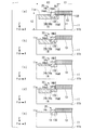
- FIG. 2 (a) to (d) show modifications of the Schottky barrier diode of the second embodiment described above.
- the same number is attached
- a part of the side surface 13S of the metal part 13 and a part of the bottom surface 13B connected thereto are in contact with a part of the p + type semiconductor part 14a.
- the p ⁇ type semiconductor portion 14b is configured to cover from the lower portion of the side surface 14bS to a part of the bottom surface 14aB of the p + type semiconductor portion 14a and not in contact with the metal portion 13.
- the p ⁇ type semiconductor part 14b is a depth at which the side surface 14bS of the p ⁇ type semiconductor part 14b and a part of the side surface 14aS of the p + type semiconductor part 14a are in contact with each other on the main surface 11a side in the peripheral part of the semiconductor substrate 11.
- the bottom surface 13B of the metal portion 13 and the bottom surface 14aB of the p + type semiconductor portion 14a are not in contact with each other.
- the p ⁇ type semiconductor part 14b is formed so as to be thinner than the thickness of the p + type semiconductor part 14a.
- the p ⁇ type semiconductor part 14b includes a part of the side surface 14bS of the p ⁇ type semiconductor part 14b and a part of the side surface 14aS of the p + type semiconductor part 14a at the peripheral part on the main surface 11a side of the semiconductor substrate 11. Is formed to a depth that makes contact with the bottom surface 13B of the metal portion 13 and the bottom surface 14aB of the p + type semiconductor portion 14a.
- the p ⁇ type semiconductor part 14b is formed to be thicker than the thickness of the p + type semiconductor part 14a.
- a p-type semiconductor portion 14 is formed on a part of the main surface 11a side of the semiconductor substrate 11.
- the p-type semiconductor portion 14 is formed so as not to contact the periphery of the semiconductor substrate 11.
- a part of the side surface 13 ⁇ / b> S of the metal part 13 and a part of the bottom surface 13 ⁇ / b> B connected thereto are in contact with a part of the p-type semiconductor part 14.
- a part of the p-type semiconductor portion 14, that is, the p-type semiconductor deposition portion 14 c is further upward from one main surface 11 a of the semiconductor substrate 11 on which the p-type semiconductor portion 14 is formed (other main surfaces 11 a as a reference).
- the surface 11b is formed up to a part of the side surface 13S of the metal portion 13 in the direction opposite to the Z-axis direction). Further, a part of the side surface 13S of the metal part 13 is configured to be in contact with the p-type semiconductor deposition portion 14c above the one main surface 11a of the semiconductor substrate 11.
- the p-type semiconductor deposition portion 14 c is formed by depositing a p + -type semiconductor by, for example, epitaxial growth so as to overlap with a region not in contact with the metal portion 13 in the p + -type semiconductor portion 14 a on the main surface 11 a side of the semiconductor substrate 11. Form. Side surface 13S of metal part 13 is in contact with p-type semiconductor deposition portion 14c.
- t1 represents the p-type semiconductor deposition portion 14c and the semiconductor substrate 11 from the other main surface 11b of the semiconductor substrate 11 to the upper surface 14cT of the p-type semiconductor deposition portion 14c in the second region E2 where the p-type semiconductor portion 14 is formed. And the total thickness t2. Thereby, the resistance value of 1st area
- a part of the side surface 13S of the metal part 13 is in contact with a part of the p-type semiconductor deposition part 14c, and a part of the p + type semiconductor part 14a.
- a part of the bottom surface 13B connected to the side surface 13S of the metal part 13 is in contact.
- the p ⁇ type semiconductor part 14b is configured to cover from the lower part of the side surface 14bS to a part of the bottom surface 14aB of the p + type semiconductor part 14a and not in contact with the metal part 13.
- a part of the side surface 13S of the metal part 13 is in contact with a part of the p-type semiconductor deposition part 14c, and a part of the p + type semiconductor part 14a.
- a part of the bottom surface 13B connected to the side surface 13S of the metal part 13 is in contact.
- the p ⁇ type semiconductor part 14b is a depth at which the side surface 14bS of the p ⁇ type semiconductor part 14b and a part of the side surface 14aS of the p + type semiconductor part 14a are in contact with each other on the main surface 11a side in the peripheral part of the semiconductor substrate 11.
- the bottom surface 13B of the metal portion 13 and the bottom portion 14aB of the p + type semiconductor portion 14a are not in contact with each other.
- the p ⁇ type semiconductor part 14b is formed so as to be thinner than the thickness of the p + type semiconductor part 14a.
- a part of the side surface 13S of the metal part 13 is in contact with a part of the p-type semiconductor deposition part 14c, and a part of the p + -type semiconductor part 14a.
- a part of the bottom surface 13B connected to the side surface 13S of the metal part 13 is in contact.
- the p ⁇ type semiconductor part 14b has a depth at which a part of the side surface 14bS of the p ⁇ type semiconductor part 14b and the side surface 14aS of the p + type semiconductor part 14a are in contact with each other on the main surface 11a side in the peripheral portion of the semiconductor substrate 11.
- the bottom surface 13B of the metal portion 13 and the bottom portion 14aB of the p + type semiconductor portion 14a are not in contact with each other.
- the p ⁇ type semiconductor part 14b is formed to be thicker than the thickness of the p + type semiconductor part 14a.
- a p-type semiconductor portion 14 is formed on a part of the main surface 11a side of the semiconductor substrate 11.
- the p-type semiconductor portion 14 is formed so as not to contact the periphery of the semiconductor substrate 11.
- a p-type semiconductor deposition portion 14c in which a p + type semiconductor is deposited is formed so as to overlap the p-type semiconductor portion 14.
- a part of the Schottky barrier diode 30 shown in FIG. 9A is the same as that of the Schottky barrier diode 10 shown in FIG.
- the end portion (edge portion) on the peripheral side of the semiconductor substrate 11 along the X-axis direction of the p ⁇ type semiconductor portion 14 b constituting the p type semiconductor portion 14 is the peripheral side of the semiconductor substrate 11.
- the thickness is gradually reduced so as to be rounded.
- the Schottky barrier diode 30 shown in FIG. 9B is partially the same as the Schottky barrier diode 30 shown in FIG.
- the p + type semiconductor part 14 a is not covered by the p ⁇ type semiconductor part 14 b, and the p + type semiconductor part 14 a is in contact with the first semiconductor region 12 at a portion overlapping the metal part 13. It has become.
- the Schottky barrier diode 30 shown in FIG. 9C is partially the same as the configuration of the Schottky barrier diode 30 shown in FIG. In this Schottky barrier diode 30, the entire bottom surface of the p + type semiconductor portion 14a is in contact with the first semiconductor region 12, and the p ⁇ type semiconductor portion 14b is thinner than the p + type semiconductor portion 14a.
- a part of the Schottky barrier diode 30 shown in FIG. 9D is the same as that of the Schottky barrier diode 30 shown in FIG. In this Schottky barrier diode 30, the entire bottom surface of the p + type semiconductor portion 14a is in contact with the first semiconductor region 12, and the p ⁇ type semiconductor portion 14b is thicker than the p + type semiconductor portion 14a.
- the Schottky barrier diode 40 shown in FIG. 10A is partially the same as the configuration of the Schottky barrier diode 20 shown in FIG. The differences are as follows. That is, in the Schottky barrier diode 40, the end portion (edge portion) side on the peripheral side of the semiconductor substrate 11 along the X-axis direction of the p ⁇ type semiconductor portion 14 b constituting the p type semiconductor portion 14 is the semiconductor substrate 11. It is configured to bulge so as to be rounded toward a position away from the peripheral edge by a predetermined distance, thereby increasing the thickness.
- the Schottky barrier diode 40 shown in FIG. 10B is partially the same as the configuration of the Schottky barrier diode 40 shown in FIG.
- the p + type semiconductor portion 14a is not covered by the p ⁇ type semiconductor portion 14b, and the p + type semiconductor portion 14a is in contact with the first semiconductor region 12 at a portion overlapping the metal portion 13. It has become.
- the Schottky barrier diode 40 shown in FIG. 10C is partially the same as the configuration of the Schottky barrier diode 40 shown in FIG. In this Schottky barrier diode 40, the entire bottom surface of the p + type semiconductor portion 14a is in contact with the first semiconductor region 12, and the p ⁇ type semiconductor portion 14b is thinner than the p + type semiconductor portion 14a.
- 10D is partially the same as the configuration of the Schottky barrier diode 40 shown in FIG.
- the entire bottom surface of the p + type semiconductor portion 14a is in contact with the first semiconductor region 12, and the p ⁇ type semiconductor portion 14b is thicker than the p + type semiconductor portion 14a.
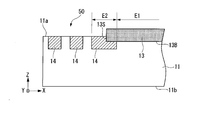
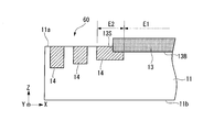
- a p-type semiconductor portion 14 is further added to the configuration of the Schottky barrier diode 10 in FIG. That is, the added p-type semiconductor portion 14 is in a position not in contact with the other p-type semiconductor portion 14 and outside the p-type semiconductor portion 14 in contact with the metal portion 13 on the peripheral side of the semiconductor substrate 11.
- a plurality of the peripheral portions of the metal portion 13 are arranged so as to surround the ring.
- the p-type semiconductor portion 14 closer to the periphery of the semiconductor substrate 11 has a thickness along the Z-axis direction increased. It is a configuration.
- the p-type semiconductor portion 14 closer to the periphery of the semiconductor substrate 11 is increased in thickness along the Z-axis direction. Yes. Furthermore, the non-formation part in which the p-type semiconductor part 14 set so as to divide a part in the circumferential direction among the annular p-type semiconductor parts 14 is formed at a different position in the Y-axis direction. Each of the semiconductor parts 14 is formed. Then, along the Y-axis direction, adjacent p-type semiconductor portions 14 are arranged so as to overlap each other.
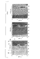
- FIGS. 4 and 5 show current flow (FIG. 4) and temperature rise in the peripheral region of the substrate when the PRSM test is performed on the conventional JBS Schottky barrier diode shown in FIG. 8 as a conventional example.
- FIG. 6 is a distribution diagram showing the distribution (FIG. 5) with the passage of time (5 ⁇ sec, 8 ⁇ sec, 20 ⁇ sec).
- the metal layer 3 is shown in the upper center, and the guard rings 6 are shown on both sides thereof.
- the Schottky barrier diode in FIGS. 4 and 5 corresponds to the conventional Schottky barrier diode shown in FIG. According to the simulation results shown in FIGS.
- the current flow does not spread over the entire Schottky junction surface in the X-axis direction and the Y-axis direction even if the time of 5 ⁇ sec, 8 ⁇ sec, and 11 ⁇ sec has elapsed since the start of the test.
- Concentrated on the portion where the guard ring 6 is formed (FIG. 4). Since the current flow does not spread over the entire Schottky junction surface in the X-axis direction and the Y-axis direction, the temperature in the vicinity of the guard ring 6 of the semiconductor substrate increases as time elapses from 5 ⁇ sec, 8 ⁇ sec, and 11 ⁇ sec from the start of the test. It was greatly increased by the current concentration (FIG. 5).
- the temperature in the vicinity of the guard ring 6 of the semiconductor substrate was 600 to 700 ° C. at the highest portion.
- the rated surge reverse power was 0.1 kW to 0.2 kW.
- FIG. 6 and FIG. 7 show an example of the present invention in which the Schottky barrier diode (semiconductor element) shown in FIG. 1A is similarly subjected to a rated surge reverse power (PRSM) test.
- FIG. 8 is a distribution diagram illustrating the flow of current (FIG. 6) and the distribution of temperature rise (FIG. 7) in the peripheral region, which are shown over time (5 ⁇ sec, 8 ⁇ sec, 20 ⁇ sec).
- FIG. 6 and FIG. 7 show an example of the present invention in which the Schottky barrier diode (semiconductor element) shown in FIG. 1A is similarly subjected to a rated surge reverse power (PRSM) test.
- FIG. 8 is a distribution diagram illustrating the flow of current (FIG. 6) and the distribution of temperature rise (FIG. 7) in the peripheral region, which are shown over time (5 ⁇ sec, 8 ⁇ sec, 20 ⁇ sec).
- a recess portion T of 0.15 ⁇ m is
- FIGS. 6 and 7 a metal part 13 is shown in the upper center, and p-type semiconductor parts 14 that are guard rings are shown on both sides thereof.
- the Schottky barrier diode in FIGS. 6 and 7 corresponds to the Schottky barrier diode of the present invention shown in FIG.
Landscapes
- Electrodes Of Semiconductors (AREA)
Abstract
Description
本発明は、上述した技術とは異なる構成によって、半導体素子、例えばショットキーバリアダイオードにおける、ショットキー接合部の逆サージ耐量を改善することを目的とする。
第一導電型である半導体基板と、前記半導体基板の一主面側の一部に形成された、前記第一導電型とは逆導電型の第二導電型である第一部位と、前記第一部位の一部と電気的に接続されるようにして、前記半導体基板の一主面側に形成された導電性の第二部位と、を少なくとも備え、
前記第一部位の一部に対して、前記第二部位は、その側面の一部とこれに連結する底面の一部とが接する構成を有することを特徴とする。
前記第二部位の底面は、前記半導体基板の厚み方向に沿って前記半導体基板の一主面よりも深い位置にあることを特徴とする。
前記第二部位の底面は、前記半導体基板の一主面に接してなり、
前記第一部位の一部は、前記半導体基板の一主面から更に上方に向けて形成されており、
前記第二部位の側面は、前記半導体基板の一主面よりも上方で前記第一部位と接することを特徴とする。
前記第一部位は、互いに不純物濃度が異なる第一濃度部と第二濃度部とからなり、
前記第一濃度部の一部に対して、前記第二部位は、その側面の一部とこれに連結する底面の一部とが接し、
前記第二濃度部は、その側面の少なくとも一部が、前記第一濃度部の側面と接してなることを特徴とする。
また、以下の図面を使用した説明において、図面は模式的なものであり、各寸法の比率等は現実のものとは異なることに留意すべきであり、理解の容易のために説明に必要な部材以外の図示は適宜省略されている。なお、以後の説明の理解を容易にするために、図面において、ダイオードの断面厚み方向をZ軸方向、Z軸方向と直交する平面方向をX軸方向およびY軸方向とする。
以下、本発明の特徴であるガードリングの内部構造を備えた半導体素子について図面を参照して詳細に説明する。
図14は、本発明に係る半導体素子の一例であるショットキーバリアダイオードの周縁領域における一実施形態を示すZ軸方向に沿った要部断面図である。
本実施形態に係るショットキーバリアダイオード(半導体素子)10は、n型(第一導電型)である半導体基板11と、この半導体基板11の一主面11a側の一部に形成された、n型とは逆導電型のp型(第二導電型)であるp型半導体部位(第一部位)14と、p型半導体部位14の一部と電気的に接続されるようにして、半導体基板11の一主面11a側に形成された導電性の金属部位(第二部位)13と、を少なくとも備えている。そして、p型半導体部位14の一部に対して、金属部位13は、その側面13Sの一部とこれに連結する底面13Bの一部とが接している。
なお、半導体基板11は、SiCに限定されず、Siから構成されていてもよい。本発明は、Si基板であっても、SiC基板であっても適用することができるが、Si基板に比べてSiC基板に適用したほうがより有用である。
しかし、上述したような構成の本発明のショットキーバリアダイオード10によれば、金属部位13と半導体基板11とがショットキー接合された第一領域E1の抵抗値を、p型半導体部位14が形成された第二領域E2の抵抗値よりも小さくすることができるため、サージ電流は、より抵抗値の小さいショットキー接合部に向けて流れる。その結果、ショットキーバリアダイオード10の逆サージ耐量を改善することが可能になる。このような本発明のショットキーバリアダイオード10を、例えばスイッチング電源に適用すれば、非常時における緊急停止などによって過大な逆方向電圧が生じても、ショットキーバリアダイオード10の機能低下を防止することが可能になる。
図1(a)は、本発明に係る半導体素子の一例であるショットキーバリアダイオードの周縁領域における一実施形態を示すZ軸方向に沿った要部断面図である。なお、図14に示す第一実施形態と同様の構成には同一の番号を付す。
本実施形態に係るショットキーバリアダイオード10は、n型である半導体基板11と、この半導体基板11の一主面11a側の一部に形成された、n型とは逆導電型のp型であるp型半導体部位14と、p型半導体部位14の一部と電気的に接続されるようにして、半導体基板11の一主面11a側に形成された導電性の金属部位13と、を少なくとも備えている。
p型半導体部位14に、例えば製造工程でコンタミネーション等が生じると、不純物イオンが注入されない領域が発生し、ショットキーバリアダイオード10の機能に影響を及ぼす懸念があるが、逆方向バイアス時には空乏層が広がるので、その影響が緩和され、サージ電流をより抵抗値の小さいショットキー接合部分に向けて確実に流すことができる効果を期待することができる。
また、一方では、結晶構造の乱れを低減するために、意図的に不純物イオンを注入しないようにすることもできる。即ち、例えば、図1(b)に示すショットキーバリアダイオード10Aのように、半導体基板11(図1(a)参照)にp+型半導体部14a、p-型半導体部14bに対応)を形成しない非形成部d1を設けることで、半導体基板11に対する不純物イオンの注入量を少なくすることができ、不純物イオン注入による半導体基板11の結晶構造の乱れを抑えることができる。こうした非形成部d1は、任意の形状であればよく、例えば、半導体基板11の一主面11a側から見て、矩形、円形、楕円形などの形状であればよい。
上述した第二実施形態のショットキーバリアダイオードの変形例を図2(a)~(d)に示す。なお、図1に示す第二実施形態と同様の構成には同一の番号を付し、その説明は省略する。
図2(a)に示すショットキーバリアダイオード10では、p+型半導体部14aの一部に対し、金属部位13の側面13Sの一部とこれに連結する底面13Bの一部とが接している。そして、p-型半導体部14bは、その側面14bSの下部からp+型半導体部14aの底面14aBの一部まで覆い、金属部位13には接しない構成となっている。
次に、図3(a)を参照しながら、第三実施形態に係るショットキーバリアダイオードについて説明する。なお、上述した第二実施形態に係るショットキーバリアダイオードと同一の構成要素には同一の符号を付して、その詳細な説明は省略する。
図3(a)に示すショットキーバリアダイオード20は、図1(a)に示すショットキーバリアダイオード20の構造の一部と同じであるが、p+型半導体部14aの構造が異なる。p型半導体部位14の一部、即ちp型半導体堆積部14cは、p型半導体部位14が形成されている半導体基板11の一主面11aから更に上方(一主面11aを基準として他の主面11bとはZ軸方向において逆の方向)に向けて金属部位13の側面13Sの一部まで形成されている。また、この金属部位13の側面13Sの一部は、半導体基板11の一主面11aよりも上方でp型半導体堆積部14cと接する構成となっている。
(4)ショットキー接合部の第三実施形態の変形例
上述した第三実施形態のショットキーバリアダイオードの変形例を図3(b)~(e)に示す。なお、図3(a)に示す第三実施形態と同様の構成には同一の番号を付し、その説明は省略する。
以下、本発明に係る半導体素子の一例であるショットキーバリアダイオードのショットキー接合部について、幾つかの変形例を例示するが、本発明はこれらの形態に限定されるものではない。なお、上述した第一実施形態、第二実施形態、および第三実施形態に係るショットキーバリアダイオードと同一の構成要素には同一の符号を付して、その詳細な説明は省略する。
図9(d)に示すショットキーバリアダイオード30は、図9(a)のショットキーバリアダイオード30の構成と一部が同じである。このショットキーバリアダイオード30においては、p+型半導体部14aの底面全体が第一半導体領域12に接し、かつ、p-型半導体部14bはp+型半導体部14aよりも厚みが厚くなっている。
図10(b)に示すショットキーバリアダイオード40は、図10(a)のショットキーバリアダイオード40の構成と一部が同じである。このショットキーバリアダイオード40においては、p+型半導体部14aがp-型半導体部14bによって覆われずに、金属部位13と重なる部分でp+型半導体部14aが第一半導体領域12に接した構成となっている。
図10(c)に示すショットキーバリアダイオード40は、図10(a)のショットキーバリアダイオード40の構成と一部が同じである。このショットキーバリアダイオード40においては、p+型半導体部14aの底面全体が第一半導体領域12に接し、かつp-型半導体部14bはp+型半導体部14aよりも厚みが薄くなっている。
図10(d)に示すショットキーバリアダイオード40は、図10(a)のショットキーバリアダイオード40の構成と一部が同じである。このショットキーバリアダイオード40においては、p+型半導体部14aの底面全体が第一半導体領域12に接し、かつ、p-型半導体部14bはp+型半導体部14aよりも厚みが厚くなっている。
本検証においては、逆サージ耐量の指標として、PRSM試験を実施した場合の、基板の周縁領域における電流の流れと温度の上昇をシミュレーションした。
図4、図5に示す分布図において、上部中央に金属層3が示され、その両側にガードリング6が示されている。この図4、図5におけるショットキーバリアダイオードは、図8に示す従来のショットキーバリアダイオードに対応する。
図4、図5に示すシミュレーション結果によれば、試験開始から時間が5μsec、8μsec、11μsecと経過しても、電流の流れはX軸方およびY軸方向のショットキー接合面全体には広がらず、ガードリング6が形成された部分に集中している(図4)。そして、電流の流れはX軸方およびY軸方向のショットキー接合面全体に広がらないため、試験開始から時間が5μsec、8μsec、11μsecと経過するに従って、半導体基板のガードリング6付近での温度が、電流の集中によって大きく上昇した(図5)。半導体基板のガードリング6付近での温度は、最も高い部分で600~700℃となった。
なお、定格サージ逆電力としては0.1kwないし0.2kwであった。
以上の結果から、従来例のショットキーバリアダイオードではガードリング付近での温度上昇によって特性低下が生じる虞があるが、本発明のショットキーバリアダイオードでは、ショットキー接合面全体の温度分布の均一化によって、特性低下が生じないというシミュレーション結果が得られた。また、定格サージ逆電力としては1kwないし2kwとなり、従来例に対して大きく改善された。
Claims (4)
- 第一導電型である半導体基板と、前記半導体基板の一主面側の一部に形成された、前記第一導電型とは逆導電型の第二導電型である第一部位と、前記第一部位の一部と電気的に接続されるようにして、前記半導体基板の一主面側に形成された導電性の第二部位と、を少なくとも備え、
前記第一部位の一部に対して、前記第二部位は、その側面の一部とこれに連結する底面の一部とが接する構成を有することを特徴とする半導体素子。 - 前記第二部位の底面は、前記半導体基板の厚み方向に沿って前記半導体基板の一主面よりも深い位置にあることを特徴とする請求項1記載の半導体素子。
- 前記第二部位の底面は、前記半導体基板の一主面に接してなり、
前記第一部位の一部は、前記半導体基板の一主面から更に上方に向けて形成されており、
前記第二部位の側面は、前記半導体基板の一主面よりも上方で前記第一部位と接することを特徴とする請求項1記載の半導体素子。 - 前記第一部位は、互いに不純物濃度が異なる第一濃度部と第二濃度部とからなり、
前記第一濃度部の一部に対して、前記第二部位は、その側面の一部とこれに連結する底面の一部とが接し、
前記第二濃度部は、その側面の少なくとも一部が、前記第一濃度部の側面と接してなることを特徴とする請求項1ないし3のいずれか1項記載の半導体素子。
Priority Applications (4)
| Application Number | Priority Date | Filing Date | Title |
|---|---|---|---|
| JP2014527988A JP5692947B1 (ja) | 2013-03-25 | 2013-03-25 | 半導体素子 |
| US14/777,673 US9653539B2 (en) | 2013-03-25 | 2013-03-25 | Semiconductor device |
| CN201380074407.2A CN105027288B (zh) | 2013-03-25 | 2013-03-25 | 半导体元件 |
| PCT/JP2013/058493 WO2014155472A1 (ja) | 2013-03-25 | 2013-03-25 | 半導体素子 |
Applications Claiming Priority (1)
| Application Number | Priority Date | Filing Date | Title |
|---|---|---|---|
| PCT/JP2013/058493 WO2014155472A1 (ja) | 2013-03-25 | 2013-03-25 | 半導体素子 |
Publications (1)
| Publication Number | Publication Date |
|---|---|
| WO2014155472A1 true WO2014155472A1 (ja) | 2014-10-02 |
Family
ID=51622568
Family Applications (1)
| Application Number | Title | Priority Date | Filing Date |
|---|---|---|---|
| PCT/JP2013/058493 Ceased WO2014155472A1 (ja) | 2013-03-25 | 2013-03-25 | 半導体素子 |
Country Status (4)
| Country | Link |
|---|---|
| US (1) | US9653539B2 (ja) |
| JP (1) | JP5692947B1 (ja) |
| CN (1) | CN105027288B (ja) |
| WO (1) | WO2014155472A1 (ja) |
Cited By (2)
| Publication number | Priority date | Publication date | Assignee | Title |
|---|---|---|---|---|
| JP2017055026A (ja) * | 2015-09-11 | 2017-03-16 | 株式会社東芝 | 半導体装置 |
| CN106796961A (zh) * | 2014-11-05 | 2017-05-31 | 新电元工业株式会社 | 半导体元件 |
Families Citing this family (2)
| Publication number | Priority date | Publication date | Assignee | Title |
|---|---|---|---|---|
| CN105493293B (zh) * | 2013-09-09 | 2018-08-24 | 株式会社日立制作所 | 半导体装置及其制造方法 |
| CN105552119A (zh) * | 2015-12-17 | 2016-05-04 | 扬州国宇电子有限公司 | 平面肖特基势垒二极管 |
Citations (5)
| Publication number | Priority date | Publication date | Assignee | Title |
|---|---|---|---|---|
| JPS5858774A (ja) * | 1981-10-05 | 1983-04-07 | Hitachi Ltd | シヨツトキ−バリア・ダイオ−ド |
| EP0849807A1 (de) * | 1996-12-20 | 1998-06-24 | General Semiconductor Ireland | Schottky-Diode |
| JP2002334998A (ja) * | 2001-05-08 | 2002-11-22 | Mitsubishi Electric Corp | 炭化珪素半導体装置およびその製造方法 |
| JP2009094392A (ja) * | 2007-10-11 | 2009-04-30 | Mitsubishi Electric Corp | 炭化珪素半導体装置の製造方法 |
| JP2009289824A (ja) * | 2008-05-27 | 2009-12-10 | Toyota Motor Corp | 半導体装置 |
Family Cites Families (7)
| Publication number | Priority date | Publication date | Assignee | Title |
|---|---|---|---|---|
| JP2585331B2 (ja) * | 1986-12-26 | 1997-02-26 | 株式会社東芝 | 高耐圧プレーナ素子 |
| JPH1117197A (ja) | 1997-06-24 | 1999-01-22 | Hitachi Ltd | ショットキーダイオードおよびその製造方法 |
| US7541660B2 (en) * | 2006-04-20 | 2009-06-02 | Infineon Technologies Austria Ag | Power semiconductor device |
| US7875950B2 (en) | 2007-03-08 | 2011-01-25 | Semiconductor Components Industries, Llc | Schottky diode structure with multi-portioned guard ring and method of manufacture |
| KR100888290B1 (ko) | 2007-08-10 | 2009-03-11 | 주식회사 케이이씨 | 쇼트키 배리어 다이오드 및 그 제조 방법 |
| KR101097984B1 (ko) * | 2010-03-26 | 2011-12-23 | 매그나칩 반도체 유한회사 | 샤키 다이오드 및 그 제조방법 |
| JP5455973B2 (ja) * | 2011-05-27 | 2014-03-26 | 三菱電機株式会社 | 炭化珪素半導体装置の製造方法 |
-
2013
- 2013-03-25 WO PCT/JP2013/058493 patent/WO2014155472A1/ja not_active Ceased
- 2013-03-25 US US14/777,673 patent/US9653539B2/en active Active
- 2013-03-25 JP JP2014527988A patent/JP5692947B1/ja active Active
- 2013-03-25 CN CN201380074407.2A patent/CN105027288B/zh active Active
Patent Citations (5)
| Publication number | Priority date | Publication date | Assignee | Title |
|---|---|---|---|---|
| JPS5858774A (ja) * | 1981-10-05 | 1983-04-07 | Hitachi Ltd | シヨツトキ−バリア・ダイオ−ド |
| EP0849807A1 (de) * | 1996-12-20 | 1998-06-24 | General Semiconductor Ireland | Schottky-Diode |
| JP2002334998A (ja) * | 2001-05-08 | 2002-11-22 | Mitsubishi Electric Corp | 炭化珪素半導体装置およびその製造方法 |
| JP2009094392A (ja) * | 2007-10-11 | 2009-04-30 | Mitsubishi Electric Corp | 炭化珪素半導体装置の製造方法 |
| JP2009289824A (ja) * | 2008-05-27 | 2009-12-10 | Toyota Motor Corp | 半導体装置 |
Cited By (3)
| Publication number | Priority date | Publication date | Assignee | Title |
|---|---|---|---|---|
| CN106796961A (zh) * | 2014-11-05 | 2017-05-31 | 新电元工业株式会社 | 半导体元件 |
| CN106796961B (zh) * | 2014-11-05 | 2020-06-19 | 新电元工业株式会社 | 半导体元件 |
| JP2017055026A (ja) * | 2015-09-11 | 2017-03-16 | 株式会社東芝 | 半導体装置 |
Also Published As
| Publication number | Publication date |
|---|---|
| US20160079347A1 (en) | 2016-03-17 |
| JP5692947B1 (ja) | 2015-04-01 |
| US9653539B2 (en) | 2017-05-16 |
| CN105027288B (zh) | 2018-09-18 |
| CN105027288A (zh) | 2015-11-04 |
| JPWO2014155472A1 (ja) | 2017-02-16 |
Similar Documents
| Publication | Publication Date | Title |
|---|---|---|
| CN102683430B (zh) | 肖特基势垒二极管 | |
| TWI596783B (zh) | Semiconductor device | |
| US7816733B2 (en) | SiC semiconductor having junction barrier schottky device | |
| JP6505625B2 (ja) | 半導体装置 | |
| KR101416361B1 (ko) | 쇼트키 배리어 다이오드 및 그 제조 방법 | |
| US9178079B2 (en) | Semiconductor diode device | |
| US10032866B2 (en) | Semiconductor device and method of manufacturing semiconductor device | |
| JP7098906B2 (ja) | ショットキーバリアダイオードを備えた炭化珪素半導体装置およびその製造方法 | |
| JP2016208030A (ja) | 半導体素子及びその製造方法 | |
| JP2015153787A (ja) | 半導体装置及び半導体装置の製造方法 | |
| JP6072349B2 (ja) | 半導体素子 | |
| JP5692947B1 (ja) | 半導体素子 | |
| JP2018010988A (ja) | 半導体装置とその製造方法 | |
| CN103872147B (zh) | 肖特基势垒二极管及其制造方法 | |
| CN103904131B (zh) | 肖特基势垒二极管及其制造方法 | |
| WO2019186785A1 (ja) | 炭化珪素半導体装置およびその製造方法 | |
| WO2015064999A1 (ko) | 접합 장벽 쇼트키 다이오드 및 이에 의해 제조된 접합 장벽 쇼트키 다이오드 | |
| KR101490937B1 (ko) | 쇼트키 배리어 다이오드 및 그 제조 방법 | |
| JP5377548B2 (ja) | 半導体整流装置 | |
| JP2015225934A (ja) | 半導体装置 |
Legal Events
| Date | Code | Title | Description |
|---|---|---|---|
| WWE | Wipo information: entry into national phase |
Ref document number: 201380074407.2 Country of ref document: CN |
|
| ENP | Entry into the national phase |
Ref document number: 2014527988 Country of ref document: JP Kind code of ref document: A |
|
| 121 | Ep: the epo has been informed by wipo that ep was designated in this application |
Ref document number: 13879764 Country of ref document: EP Kind code of ref document: A1 |
|
| WWE | Wipo information: entry into national phase |
Ref document number: 14777673 Country of ref document: US |
|
| NENP | Non-entry into the national phase |
Ref country code: DE |
|
| 122 | Ep: pct application non-entry in european phase |
Ref document number: 13879764 Country of ref document: EP Kind code of ref document: A1 |