WO2014141893A1 - 電子機器 - Google Patents
電子機器 Download PDFInfo
- Publication number
- WO2014141893A1 WO2014141893A1 PCT/JP2014/054966 JP2014054966W WO2014141893A1 WO 2014141893 A1 WO2014141893 A1 WO 2014141893A1 JP 2014054966 W JP2014054966 W JP 2014054966W WO 2014141893 A1 WO2014141893 A1 WO 2014141893A1
- Authority
- WO
- WIPO (PCT)
- Prior art keywords
- hole
- input device
- display
- display panel
- electronic device
- Prior art date
- Legal status (The legal status is an assumption and is not a legal conclusion. Google has not performed a legal analysis and makes no representation as to the accuracy of the status listed.)
- Ceased
Links
Images




Classifications
-
- G—PHYSICS
- G06—COMPUTING OR CALCULATING; COUNTING
- G06F—ELECTRIC DIGITAL DATA PROCESSING
- G06F1/00—Details not covered by groups G06F3/00 - G06F13/00 and G06F21/00
- G06F1/16—Constructional details or arrangements
- G06F1/1613—Constructional details or arrangements for portable computers
- G06F1/1633—Constructional details or arrangements of portable computers not specific to the type of enclosures covered by groups G06F1/1615 - G06F1/1626
- G06F1/1684—Constructional details or arrangements related to integrated I/O peripherals not covered by groups G06F1/1635 - G06F1/1675
-
- G—PHYSICS
- G02—OPTICS
- G02F—OPTICAL DEVICES OR ARRANGEMENTS FOR THE CONTROL OF LIGHT BY MODIFICATION OF THE OPTICAL PROPERTIES OF THE MEDIA OF THE ELEMENTS INVOLVED THEREIN; NON-LINEAR OPTICS; FREQUENCY-CHANGING OF LIGHT; OPTICAL LOGIC ELEMENTS; OPTICAL ANALOGUE/DIGITAL CONVERTERS
- G02F1/00—Devices or arrangements for the control of the intensity, colour, phase, polarisation or direction of light arriving from an independent light source, e.g. switching, gating or modulating; Non-linear optics
- G02F1/01—Devices or arrangements for the control of the intensity, colour, phase, polarisation or direction of light arriving from an independent light source, e.g. switching, gating or modulating; Non-linear optics for the control of the intensity, phase, polarisation or colour
- G02F1/13—Devices or arrangements for the control of the intensity, colour, phase, polarisation or direction of light arriving from an independent light source, e.g. switching, gating or modulating; Non-linear optics for the control of the intensity, phase, polarisation or colour based on liquid crystals, e.g. single liquid crystal display cells
- G02F1/133—Constructional arrangements; Operation of liquid crystal cells; Circuit arrangements
- G02F1/1333—Constructional arrangements; Manufacturing methods
-
- G—PHYSICS
- G06—COMPUTING OR CALCULATING; COUNTING
- G06F—ELECTRIC DIGITAL DATA PROCESSING
- G06F1/00—Details not covered by groups G06F3/00 - G06F13/00 and G06F21/00
- G06F1/16—Constructional details or arrangements
- G06F1/1613—Constructional details or arrangements for portable computers
- G06F1/1633—Constructional details or arrangements of portable computers not specific to the type of enclosures covered by groups G06F1/1615 - G06F1/1626
- G06F1/1637—Details related to the display arrangement, including those related to the mounting of the display in the housing
-
- G—PHYSICS
- G09—EDUCATION; CRYPTOGRAPHY; DISPLAY; ADVERTISING; SEALS
- G09G—ARRANGEMENTS OR CIRCUITS FOR CONTROL OF INDICATING DEVICES USING STATIC MEANS TO PRESENT VARIABLE INFORMATION
- G09G3/00—Control arrangements or circuits, of interest only in connection with visual indicators other than cathode-ray tubes
- G09G3/20—Control arrangements or circuits, of interest only in connection with visual indicators other than cathode-ray tubes for presentation of an assembly of a number of characters, e.g. a page, by composing the assembly by combination of individual elements arranged in a matrix no fixed position being assigned to or needed to be assigned to the individual characters or partial characters
- G09G3/34—Control arrangements or circuits, of interest only in connection with visual indicators other than cathode-ray tubes for presentation of an assembly of a number of characters, e.g. a page, by composing the assembly by combination of individual elements arranged in a matrix no fixed position being assigned to or needed to be assigned to the individual characters or partial characters by control of light from an independent source
- G09G3/36—Control arrangements or circuits, of interest only in connection with visual indicators other than cathode-ray tubes for presentation of an assembly of a number of characters, e.g. a page, by composing the assembly by combination of individual elements arranged in a matrix no fixed position being assigned to or needed to be assigned to the individual characters or partial characters by control of light from an independent source using liquid crystals
- G09G3/3611—Control of matrices with row and column drivers
- G09G3/3648—Control of matrices with row and column drivers using an active matrix
-
- G—PHYSICS
- G02—OPTICS
- G02F—OPTICAL DEVICES OR ARRANGEMENTS FOR THE CONTROL OF LIGHT BY MODIFICATION OF THE OPTICAL PROPERTIES OF THE MEDIA OF THE ELEMENTS INVOLVED THEREIN; NON-LINEAR OPTICS; FREQUENCY-CHANGING OF LIGHT; OPTICAL LOGIC ELEMENTS; OPTICAL ANALOGUE/DIGITAL CONVERTERS
- G02F1/00—Devices or arrangements for the control of the intensity, colour, phase, polarisation or direction of light arriving from an independent light source, e.g. switching, gating or modulating; Non-linear optics
- G02F1/01—Devices or arrangements for the control of the intensity, colour, phase, polarisation or direction of light arriving from an independent light source, e.g. switching, gating or modulating; Non-linear optics for the control of the intensity, phase, polarisation or colour
- G02F1/13—Devices or arrangements for the control of the intensity, colour, phase, polarisation or direction of light arriving from an independent light source, e.g. switching, gating or modulating; Non-linear optics for the control of the intensity, phase, polarisation or colour based on liquid crystals, e.g. single liquid crystal display cells
- G02F1/133—Constructional arrangements; Operation of liquid crystal cells; Circuit arrangements
- G02F1/1333—Constructional arrangements; Manufacturing methods
- G02F1/133302—Rigid substrates, e.g. inorganic substrates
-
- G—PHYSICS
- G02—OPTICS
- G02F—OPTICAL DEVICES OR ARRANGEMENTS FOR THE CONTROL OF LIGHT BY MODIFICATION OF THE OPTICAL PROPERTIES OF THE MEDIA OF THE ELEMENTS INVOLVED THEREIN; NON-LINEAR OPTICS; FREQUENCY-CHANGING OF LIGHT; OPTICAL LOGIC ELEMENTS; OPTICAL ANALOGUE/DIGITAL CONVERTERS
- G02F1/00—Devices or arrangements for the control of the intensity, colour, phase, polarisation or direction of light arriving from an independent light source, e.g. switching, gating or modulating; Non-linear optics
- G02F1/01—Devices or arrangements for the control of the intensity, colour, phase, polarisation or direction of light arriving from an independent light source, e.g. switching, gating or modulating; Non-linear optics for the control of the intensity, phase, polarisation or colour
- G02F1/13—Devices or arrangements for the control of the intensity, colour, phase, polarisation or direction of light arriving from an independent light source, e.g. switching, gating or modulating; Non-linear optics for the control of the intensity, phase, polarisation or colour based on liquid crystals, e.g. single liquid crystal display cells
- G02F1/133—Constructional arrangements; Operation of liquid crystal cells; Circuit arrangements
- G02F1/1333—Constructional arrangements; Manufacturing methods
- G02F1/133308—Support structures for LCD panels, e.g. frames or bezels
-
- G—PHYSICS
- G02—OPTICS
- G02F—OPTICAL DEVICES OR ARRANGEMENTS FOR THE CONTROL OF LIGHT BY MODIFICATION OF THE OPTICAL PROPERTIES OF THE MEDIA OF THE ELEMENTS INVOLVED THEREIN; NON-LINEAR OPTICS; FREQUENCY-CHANGING OF LIGHT; OPTICAL LOGIC ELEMENTS; OPTICAL ANALOGUE/DIGITAL CONVERTERS
- G02F1/00—Devices or arrangements for the control of the intensity, colour, phase, polarisation or direction of light arriving from an independent light source, e.g. switching, gating or modulating; Non-linear optics
- G02F1/01—Devices or arrangements for the control of the intensity, colour, phase, polarisation or direction of light arriving from an independent light source, e.g. switching, gating or modulating; Non-linear optics for the control of the intensity, phase, polarisation or colour
- G02F1/13—Devices or arrangements for the control of the intensity, colour, phase, polarisation or direction of light arriving from an independent light source, e.g. switching, gating or modulating; Non-linear optics for the control of the intensity, phase, polarisation or colour based on liquid crystals, e.g. single liquid crystal display cells
- G02F1/133—Constructional arrangements; Operation of liquid crystal cells; Circuit arrangements
- G02F1/1333—Constructional arrangements; Manufacturing methods
- G02F1/13338—Input devices, e.g. touch panels
-
- G—PHYSICS
- G02—OPTICS
- G02F—OPTICAL DEVICES OR ARRANGEMENTS FOR THE CONTROL OF LIGHT BY MODIFICATION OF THE OPTICAL PROPERTIES OF THE MEDIA OF THE ELEMENTS INVOLVED THEREIN; NON-LINEAR OPTICS; FREQUENCY-CHANGING OF LIGHT; OPTICAL LOGIC ELEMENTS; OPTICAL ANALOGUE/DIGITAL CONVERTERS
- G02F1/00—Devices or arrangements for the control of the intensity, colour, phase, polarisation or direction of light arriving from an independent light source, e.g. switching, gating or modulating; Non-linear optics
- G02F1/01—Devices or arrangements for the control of the intensity, colour, phase, polarisation or direction of light arriving from an independent light source, e.g. switching, gating or modulating; Non-linear optics for the control of the intensity, phase, polarisation or colour
- G02F1/13—Devices or arrangements for the control of the intensity, colour, phase, polarisation or direction of light arriving from an independent light source, e.g. switching, gating or modulating; Non-linear optics for the control of the intensity, phase, polarisation or colour based on liquid crystals, e.g. single liquid crystal display cells
- G02F1/133—Constructional arrangements; Operation of liquid crystal cells; Circuit arrangements
- G02F1/1333—Constructional arrangements; Manufacturing methods
- G02F1/1335—Structural association of cells with optical devices, e.g. polarisers or reflectors
- G02F1/133526—Lenses, e.g. microlenses or Fresnel lenses
-
- G—PHYSICS
- G02—OPTICS
- G02F—OPTICAL DEVICES OR ARRANGEMENTS FOR THE CONTROL OF LIGHT BY MODIFICATION OF THE OPTICAL PROPERTIES OF THE MEDIA OF THE ELEMENTS INVOLVED THEREIN; NON-LINEAR OPTICS; FREQUENCY-CHANGING OF LIGHT; OPTICAL LOGIC ELEMENTS; OPTICAL ANALOGUE/DIGITAL CONVERTERS
- G02F1/00—Devices or arrangements for the control of the intensity, colour, phase, polarisation or direction of light arriving from an independent light source, e.g. switching, gating or modulating; Non-linear optics
- G02F1/01—Devices or arrangements for the control of the intensity, colour, phase, polarisation or direction of light arriving from an independent light source, e.g. switching, gating or modulating; Non-linear optics for the control of the intensity, phase, polarisation or colour
- G02F1/13—Devices or arrangements for the control of the intensity, colour, phase, polarisation or direction of light arriving from an independent light source, e.g. switching, gating or modulating; Non-linear optics for the control of the intensity, phase, polarisation or colour based on liquid crystals, e.g. single liquid crystal display cells
- G02F1/133—Constructional arrangements; Operation of liquid crystal cells; Circuit arrangements
- G02F1/1333—Constructional arrangements; Manufacturing methods
- G02F1/1339—Gaskets; Spacers; Sealing of cells
-
- G—PHYSICS
- G02—OPTICS
- G02F—OPTICAL DEVICES OR ARRANGEMENTS FOR THE CONTROL OF LIGHT BY MODIFICATION OF THE OPTICAL PROPERTIES OF THE MEDIA OF THE ELEMENTS INVOLVED THEREIN; NON-LINEAR OPTICS; FREQUENCY-CHANGING OF LIGHT; OPTICAL LOGIC ELEMENTS; OPTICAL ANALOGUE/DIGITAL CONVERTERS
- G02F2201/00—Constructional arrangements not provided for in groups G02F1/00 - G02F7/00
- G02F2201/56—Substrates having a particular shape, e.g. non-rectangular
Definitions
- the present invention relates to an electronic device including a display panel.
- a transmissive liquid crystal display device includes a liquid crystal panel, a backlight device, a circuit board and a power source for supplying various electric signals to the liquid crystal panel, and a housing for housing these.
- the liquid crystal panel is provided with a display area (active area) in which a plurality of pixels are arranged and a frame area (inactive area) located outside the display area.
- a display area active area
- a frame area inactive area
- pixel electrodes, TFTs, and the like are provided, and images and videos are displayed.
- a seal portion for sealing the liquid crystal material between the substrates, wiring connected to the scanning line or signal line, a monolithic drive circuit, a terminal connected to an external drive circuit, etc. Is arranged and is not used for displaying images and videos.
- the frame area of the liquid crystal panel is an area that does not contribute to display, it is preferable that the frame area be narrowed. However, although the narrowing of the frame of the liquid crystal panel is progressing year by year, it is theoretically difficult to eliminate the frame area.
- the convex curved surface portion (lens portion) of the translucent cover typically covers the frame area of the display panel and a part of the display area in the vicinity of the frame area (hereinafter sometimes referred to as a peripheral display area).
- a peripheral display area a part of the display area in the vicinity of the frame area.
- the light emitted from the pixels (peripheral pixels) arranged in the peripheral display area is refracted in the lens unit, and as a result, the image formed by the peripheral pixels is enlarged and displayed in front of the frame area.
- the observer seems to have an image on the frame area, so that the frame area becomes inconspicuous or the frame area does not exist.
- the display device as described above is used, for example, in a portable electronic device (smartphone or the like), it is possible to provide almost the entire area of the panel surface on the viewer side of the electronic device as a displayable region.
- Such an electronic device is advantageous from the viewpoint of downsizing the device because the area where information can be displayed is larger than the size of the device.
- an electronic device exhibiting near-future stylishness it seems that it will inspire people widely.
- buttons and cameras are arranged outside the display panel, such as a frame area of the display panel. Therefore, in an electronic device designed to eliminate the frame area as described above, there is a problem of how to arrange buttons and the like.
- buttons for example, on the back or side of the electronic device, not on the front.
- positions a touch panel in the whole panel surface by the side of an observer, and makes a touch panel perform the function replaced with a button switch, and excludes a physical switch from the panel front surface is also considered. In this way, it is possible to obtain a display area with the maximum area.
- the present invention has been made to solve the above-described problems, and provides an electronic device having a display panel that can expand a display usable area on the front surface of the panel without impairing user convenience.
- the purpose is to do.
- An electronic device is a display panel that includes a substrate and includes a display region and a frame region located outside the display region on the substrate, and the display device includes the display region on the inner side of the frame region.
- a display panel provided with a hole penetrating the substrate and having a non-display area formed around the hole; and a portion projecting from the display panel on one side of the substrate, the position corresponding to the hole
- An input device provided and a circuit board provided on the other side of the substrate are provided, and the input device is connected to the circuit substrate through the hole.
- the input device at least partially covers the non-display area formed around the hole.
- a separate wiring region having a wiring pattern different from another region is formed around the hole, the non-display region includes the separate wiring region, and the input device includes the separate wiring region. Covering at least partially.
- the electronic device includes a light-transmitting cover that covers at least a part of the display panel, and the light-transmitting cover includes a lens portion having a curved surface around the hole. .
- the translucent cover covers at least a peripheral region of the hole of the display panel and has another lens portion in a region corresponding to an end portion of the display panel.
- the display panel includes a pair of substrates including the substrate and a display medium layer held between the pair of substrates, and the non-display area formed around the hole includes the display panel.
- a seal portion for sealing a space between the pair of substrates is provided.
- the input device has a size larger than the hole and protrudes from a viewer-side surface of the display panel, and is connected to the first part and disposed in the hole. And a second part.
- the image processing unit includes an image processing unit that generates image data to be supplied to the display panel, and the image processing unit displays image data for displaying an image related to the input device around the input device. It is configured so that it can be generated.
- the image related to the input device is an image for operating the input device.
- the input device is configured to be directly operable by a user, and a signal is supplied to the circuit board in accordance with the operation of the user.
- the input device includes a light receiving element.
- the input device includes an image sensor and a fiber optic face plate disposed in front of the image sensor.
- the fiber optic face plate is a taper type, and the area of the end face on the viewer side of the display panel is larger than the area of the other end face.
- the display panel is a liquid crystal display panel.
- the electronic device According to the electronic device according to the embodiment of the present invention, it is possible to obtain a display area that is relatively large with respect to the size of the device without deteriorating the convenience for the user.
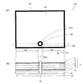
- FIG. 1A and 1B are views for explaining an electronic apparatus according to a first embodiment of the present invention, wherein FIG. 1A is a plan view when viewed from an observer side, and FIG. 1B is along a line xx ′ in FIG. FIG.
- FIG. 1A is a plan view when viewed from an observer side
- FIG. 1B is along a line xx ′ in FIG.
- FIG. 1 It is a figure for demonstrating the electronic device by the comparative form of this invention, (a) is a top view when it sees from an observer side, (b) is along the xx 'line
- FIG. 7 is a cross-sectional view showing an electronic apparatus according to Embodiment 2 of the present invention, and (a) to (c) show different forms, respectively.
- FIG. 10 is a diagram for explaining an electronic apparatus according to a third embodiment of the present invention, (a) is a plan view when viewed from the observer side, and (b) is along the line xx ′ of (a).
- FIG. It is sectional drawing which expands and shows a part of electronic device shown to Fig.8 (a) and (b).
- 7A and 7B are diagrams for explaining an electronic device according to a fourth embodiment of the present invention, FIG. 5A is a plan view when viewed from the observer side, and FIG. 5B is along the line xx ′ of FIG. FIG.
- FIG. 1 It is a figure for demonstrating the fiber optic faceplate (FOP) with which the electronic device of Embodiment 4 is provided, (a) is a side view which shows the arrangement
- the present inventors diligently studied the arrangement of input devices such as button switches and cameras in electronic devices having a display panel with a narrow frame. As a result, by arranging these input devices in the display area of the display panel instead of the frame area, the displayable area can be expanded without impairing the convenience of the user. It was concluded that the enlarged displayable area can be used effectively. According to the configuration in which the input device is arranged in the display area, an image can be displayed even on the entire periphery of the front surface of the panel of the electronic device.
- an operation button (such as a cross key) of a portable game machine can be cited.
- operation buttons are preferably arranged on the observer side surface (panel front surface) of the device.
- the operation buttons are provided in other places or reproduced by software on the touch panel, the user operability is significantly deteriorated.
- a front camera for projecting a user's face or the like is required to be provided on the front surface of the panel for the convenience of using the screen in a video phone or the like.
- a liquid crystal layer In the display area of the display panel, a liquid crystal layer, a light emitting diode, and the like are arranged, and a plurality of pixels are provided.
- a liquid crystal layer In the case of a liquid crystal panel, a liquid crystal layer is held in a space sealed by a seal portion disposed in a frame area, and the display area is provided in a space where the liquid crystal layer is sealed.
- the input device as described above has not been provided in the display area of the display panel.
- the reason is that the input device is often connected to a circuit board or the like arranged on the back side of the liquid crystal panel, and arranging the input device in the display area is considered to be accompanied by a great difficulty in manufacturing. Because it was.
- a frame region having a certain area is usually provided, there is no need to dare to arrange an input device in the display region.
- a sealing material is disposed not only at the periphery of the panel but also around the hole, and the hole is formed after the substrates are bonded together, so that the liquid crystal is not greatly affected in other regions Panels can be made.
- the liquid crystal layer is formed, for example, by placing a sealing material around the periphery of the panel or around the hole, dropping the liquid crystal on one side of the substrate before bonding the substrates, and then bonding the substrates together. be able to.
- a liquid crystal layer can be formed by injecting liquid crystal after disposing a sealing material around the periphery of the panel or around the hole and bonding the substrates together.
- conductive patterns for driving the pixels are arranged.
- wiring can be performed so as to avoid the hole, and an image or the like can be appropriately displayed in other regions excluding the hole and its periphery.
- a sealing material for sealing the liquid crystal is provided around the hole.
- a non-display area is also formed around the hole.
- the periphery of the hole can be made inconspicuous. This provides a sense of unity as a device.
- a translucent cover may be provided on the viewer side of the display panel, and a lens portion may be provided on the translucent cover around the hole.
- liquid crystal panels having holes in the display area are disclosed in, for example, Patent Documents 2 to 4.
- the display devices described in Patent Documents 2 to 4 do not disclose a configuration in which an input device is disposed in this hole. Further, it does not disclose a configuration that makes the periphery of the hole inconspicuous and can provide a sense of unity between the input device and the display panel.
- input devices provided in an electronic apparatus include various physical and electrical switches that receive input from a user, buttons, optical elements that can receive external light, and the like. It may be a device.
- the input device receives an input (direct operation) from the user, a push button, a direction key (cross key), an analog stick, a touch panel, a rotary switch (volume controller), a rotary selector (jog dial), Includes toggle switches, trackballs, trackpads, stick-type pointing devices, hardware keyboards and more.
- the input device includes an image sensor (CCD image sensor, CMOS image sensor, etc.), a light receiving element (fiber optic face plate, etc.), an optical sensor, etc. that receive optical input.
- image sensor CCD image sensor, CMOS image sensor, etc.
- light receiving element fiber optic face plate, etc.
- optical sensor etc. that receive optical input.
- it may be a temperature sensor, a microphone, an input terminal such as HDMI (registered trademark) or USB, or a wiring terminal such as a plug or an outlet.
- These input devices are physically, electrically, or optically connected to a circuit board disposed on the back side of the display panel. Input from the input device may be processed on the circuit board. With such a configuration, user convenience can be ensured while increasing the displayable area on the panel surface.
- the electronic device may be various electronic devices such as a portable game machine, a smartphone, a mobile phone, a PDA, a tablet terminal, an electronic book reader, a music player, a camera, an electronic dictionary, and an electronic device. It may be a notebook, navigation system, display device, personal computer, wearable computer, game machine, television, information display, or the like.
- FIG. 1A and 1B are diagrams illustrating a configuration of an electronic device 100 according to the first embodiment.
- FIG. 1A is a plan view when viewed from a user
- FIG. 1B is an xx ′ line in FIG. It is sectional drawing along a line.
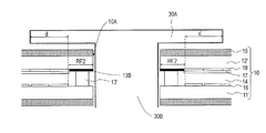
- FIG. 3 is an enlarged cross-sectional view showing a region in the vicinity of the hole 10 ⁇ / b> A provided in the display panel 10 in the electronic device 100.
- the electronic device 100 of the first embodiment includes a liquid crystal panel (display panel) 10 and a circuit board 20 disposed on the back side of the liquid crystal panel 10 (on the side opposite to the observer side).
- the liquid crystal panel 10 of the present embodiment is a transmissive type, and a backlight 40 is provided between the liquid crystal panel 10 and the circuit board 20.
- the backlight 40 may be an edge light type backlight including optical elements such as a light guide plate, a diffusion plate, and a reflection plate in addition to a light source such as an LED, or may be a direct type (surface emitting type) backlight. There may be.
- the liquid crystal panel 10 includes a TFT substrate 11, a counter substrate 12 facing the TFT substrate 11, and a liquid crystal layer 14 held between the pair of substrates.
- the liquid crystal layer 14 is sealed between the substrates 11 and 12 by a seal portion 13 provided in the peripheral frame region RF and a seal portion 13 'around the hole 10A described later.
- the TFT substrate 11 has a configuration in which a pixel electrode (transparent electrode) 16 and the like are provided on a transparent substrate 11 '.
- the counter substrate 12 has a configuration in which a common electrode (transparent electrode) 17 and a color filter 18 are provided on a transparent substrate 12 '.
- the optical film layer 15 which consists of a polarizing plate, a phase difference film, etc. is affixed on the outer surface of the TFT substrate 11 and the counter substrate 12 via the adhesion layer.
- these are exemplary, and the liquid crystal panel 10 can have various known configurations.
- the liquid crystal panel 10 is provided with a display area (active area) RA in which pixels are arranged and a frame area RF (hereinafter also referred to as a peripheral frame area RF) provided on the outside thereof.
- a display area RA the area inside the frame area RF formed around the liquid crystal panel 10 is called a display area RA for convenience.
- the display area RA may include an area that does not contribute to display.
- a hole 10A penetrating the liquid crystal panel 10 is provided inside the peripheral frame area RF of the liquid crystal panel 10 (that is, in the display area RA). Further, a non-display area RF2 is formed around the hole 10A.
- the hole 10A passes through the TFT substrate 11, the counter substrate 12, the liquid crystal layer 14, and the like. Furthermore, the hole 10 ⁇ / b> A also penetrates the backlight 40.
- the diameter of the hole 10A may be selected as appropriate, but is set to 1 mm to 15 mm, for example.
- the case where the planar shape of the hole 10A is circular is illustrated, but the hole 10A may have another arbitrary planar shape such as a quadrangle.
- the hole 10A is arranged in the display area RA, but is not an area contributing to display because pixels are not arranged.
- An annular non-display area RF2 including a seal portion 13 'and a black matrix (not shown) is formed around the hole 10A.
- the non-display area RF2 is also arranged in a display area (active area) RA defined as an area inside the frame area RF, but is not an area contributing to display.
- the electronic device 100 is provided with an input device 30 arranged so as to pass through the hole 10A provided in the display area RA.
- the input device 30 is a push-type electric switch, for example, a hardware button provided on a smartphone.
- the input device 30 is connected to the front surface portion (switch cap) 30 ⁇ / b> A that is a portion protruding from the viewer-side surface of the liquid crystal panel 10 and the front surface portion 30 ⁇ / b> A, and is disposed inside the hole 10 ⁇ / b> A of the liquid crystal panel 10. And an extended portion 30B. Further, the input device 30 has a connector portion 30 ⁇ / b> C provided on the circuit board 20. In such a configuration, the input device 30 is connected to the circuit board 20 by the connector portion 30C.
- the front part 30A arranged on the user side (observer side) of the input device 30 is provided as a widened portion having a diameter larger than the diameter of the hole 10A.
- the front surface portion 30A covers the hole 10A and the non-display area RF2 provided around the hole 10A.
- the input device 30 Since the input device 30 has a widened portion having a diameter larger than the diameter of the hole 10A, it is difficult to mount the input device 30 on the circuit board unless the front surface portion 30A and the extended portion 30B are connected as described above. There is a case. In the case of the connected configuration, after mounting the extension portion 30B on the circuit board, the front portion 30A is fitted after passing through the hole 10A of the liquid crystal panel, thereby enabling easy assembly.
- FIG. 3 shows an enlarged view of the vicinity of the front surface portion 30A.
- the non-display region RF2 existing around the hole 10A includes a seal portion 13 ′ around the hole and a light shielding region (black matrix) 13B for preventing light leakage. It is out. Since the light shielding region 13B is made of black resin or the like, it is easily noticeable. Therefore, the front surface portion 30A is preferably formed so as to hide the non-display region RF2 including the seal portion 13 'and the light shielding region 13B from the user.
- the front surface portion 30A is formed so as to cover an area outside the non-display area RF2 by a distance (tolerance) d.
- a distance (tolerance) d is because the non-display area RF2 is more reliably covered with the front face portion 30A even when the non-display area RF2 and the front face portion 30A are misaligned or the front face portion 30A is misaligned in the manufacturing process. Because it can be.
- the distance d is set to about 0.1 mm, for example.
- the non-display region RF2 is defined as a region between the pixel electrodes 16 arranged to face each other with the hole 10A interposed therebetween.
- the liquid crystal panel 10 of the present embodiment has a hole 10A.
- matrix wiring around the hole 10A may be formed so as to avoid the hole 10A.
- the wiring pitch may be clogged.
- the aperture ratio may be reduced around this area. Therefore, the front surface portion 30A may be provided so as to cover at least a part of a region where wiring is clogged (sometimes referred to as a separate wiring region). As a result, areas that are difficult to use for display can be collected and made inconspicuous by the front surface portion 30A.
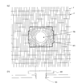
- FIG. 12A shows an example of wiring on the TFT substrate around the hole 10A.
- both the source wiring 4 extending in the vertical direction and the gate wiring 2 extending in the horizontal direction perpendicular thereto are provided so as to bypass the hole 10A.
- pixels can be provided in a matrix in a region other than the periphery of the hole 10A, and the pixel electrode 16 (see the drawing) connected to the TFT (not shown) using the source wiring 4 and the gate wiring 2 is used.
- a predetermined voltage can be applied to display an image or the like.
- a TFT may have a channel formed from an oxide semiconductor layer such as an In—Ga—Zn—O-based semiconductor layer.
- another wiring region RF3 including a detouring wiring is provided around the hole 10A.
- the separate wiring region RF3 is a region where the aperture ratio is low and it is difficult to arrange pixels. Since the separate wiring region RF3 cannot be used for display, it may be covered with a black matrix.
- the separate wiring region RF3 is covered with the front surface portion 30A of the input device 30. Accordingly, since the separate wiring area RF3 can be hidden from the user, a configuration with a sense of unity between the front surface portion 30A and the display area RA can be provided to the user.
- the input device 30 arranged in the display area RA has a sense of unity with the display panel 10.
- FIG. 2 is a diagram illustrating a configuration of a comparative electronic device 900
- FIG. 2 (a) is a plan view when viewed from the viewer side
- FIG. 2 (b) is illustrated in FIG. 2 (a).
- FIG. 6 is a cross-sectional view along the line xx ′. Components similar to those of the electronic device 900 illustrated in FIG. 1 are denoted by the same reference numerals and description thereof is omitted.
- the hole 10A and a non-display region RF2 formed in an annular shape around the hole 10A are formed.
- this portion becomes conspicuous. For this reason, compared with the electronic device 100 of Embodiment 1, the sense of unity between the input device and the display panel is impaired.
- the width of the non-display area RF2 is thicker than the width of the peripheral frame area RF, it is preferable to hide the non-display area RF2 because it is easily noticeable. Note that the reason why the width of the non-display area RF2 becomes wider is that it is difficult to provide pixels around the hole 10A because the wiring is formed so as to bypass the hole, and this may be covered with a black matrix. Because.
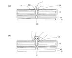
- FIG. 4A is a diagram for explaining a use situation of the input device 30 by the user, and here, a case where the push button type switch 30 is used as the input device is shown.
- the user can perform an operation of pressing a button (front portion 30A of the switch 30) arranged in the display area RA.
- a button front portion 30A of the switch 30
- By depressing this button 30A it is possible to determine that an input (button depressing) has been performed, for example, by connecting an electrical contact in the connector portion 30C arranged on the circuit board 20.
- a structure of a pushbutton type switch since a well-known structure can be utilized, it does not explain in detail here.
- FIG. 4B is a diagram illustrating a usage state of the input device which is the rotary switch 32.
- the user can perform an operation of rotating the rotary switch 32 disposed in the display area and connected to the circuit board 20 through the hole 10A.
- the rotation operation of the switch may be received as an electrical signal at a connector portion arranged on the circuit board 20.
- a structure of the rotary switch 32 since a well-known structure can be utilized, it does not explain in detail here.
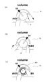
- FIGS. 5A to 5C show a state where a rotary switch 32 as an input device is provided in the display area RA.
- the electronic device may be configured to display an image and information related to the rotary switch 32 in the display area RA.
- the electronic device may be configured to display the current volume size around the rotary switch 32 according to the operation of the rotary switch 32 by the user. Good.
- FIG. 5C shows a comparative electronic device.
- a state is shown in which the rotary switch protruding from the display panel does not cover the non-display area RF2 formed around the hole.
- the non-display area RF2 is observed by the user between the display image displayed in the display area RA and the switch.
- a user does not perform intuitive operation easily.
- the sense of unity between the switch and the image is reduced.
- a known image processing apparatus image processing unit or the like can be used for displaying an image related to the input device around the input device on the display panel.
- the image processing apparatus may include, for example, an arithmetic processing unit or a graphic processing unit provided on a circuit board.
- the image processing apparatus is configured to be able to generate image data that determines an image to be displayed on the display panel, and by appropriately controlling this, the related image can be displayed around the input device. it can.
- FIGS. 6A and 6B show electronic devices 102 and 104 according to modifications.
- a touch panel 50 and a translucent cover (front plate) 52 are provided on the viewer side of the display panel 10.
- the touch panel 50 may have a known configuration.
- the translucent cover 52 is typically made of translucent glass or resin material.
- the translucent cover 52 and the touch panel 50 may be integrally formed.
- the front surface portion 30A of the input device 30 protrudes from the user-side surface of the display panel 10.
- the surface of the front surface portion 30 ⁇ / b> A exists at a position at substantially the same level as the surface of the translucent cover 52. According to such an arrangement, unevenness is hardly formed on the user-side surface of the electronic device 102, so that the appearance is good.
- the input device 30 is a push button, the possibility of inadvertently pressing a switch can be reduced.
- the structure which can make the foremost front surface of the translucent cover 52 flat is preferable on design, and is particularly suitable for electronic devices in which thinness is particularly important, such as mobile phones, smartphones, and tablets.
- the front surface portion 30A of the input device 30 protrudes not only from the user side surface of the display panel 10, but also from the surface of the touch panel 50 and the translucent cover 52.
- the input device 30 is a rotary switch or the like, the user operability is improved with such a configuration.
- the front surface portion 30A of the input device 30 preferably covers the non-display area RF2 around the hole 10A.
- the hole 10A can be made inconspicuous, and a sense of unity between the input device 30 and the display panel 10 can be obtained.
- the touch panel 50 and the translucent cover 52 are also provided with holes at corresponding positions.
- the input device 30 is a device that does not require direct input by the user, such as a light receiving element
- the touch panel 50 and the translucent cover 52 do not have holes, and the input device 30 front surface portions 30A may be covered.
- FIGS. 6A and 6B show a form in which an out-cell type touch panel 50 is provided on the viewer side of the display panel 10, but the embodiment of the present invention is in such a form. Not limited. Instead of the out-cell type touch panel 50, an on-cell type or in-cell type touch panel may be used. When an in-cell type touch panel is used, the touch panel is configured inside the display panel 10.
- the non-display area (for example, the area where the seal portion or the pixel electrode is not formed, and the component and the display panel) exist in the display panel by an input device such as a switch.
- the area including the gaps) can be concealed, so a design can be realized in which the switch blends into the display screen without a sense of incongruity.
- the switch operation and the image there are advantages that the user's usability is greatly improved and that various operations can be performed with few switches.
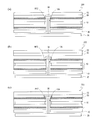
- FIG. 7A is a cross-sectional view illustrating the electronic device 200 according to the second embodiment.
- FIGS. 7B and 7C are cross-sectional views showing different modifications 202 and 204, respectively.
- the electronic devices 200, 202, and 204 of the second embodiment include an optical device as an input device.
- the same referential mark is attached
- the 7A includes a display panel 10, a backlight 40, and a circuit board 20.
- the electronic apparatus 200 illustrated in FIG. In the display area of the display panel 10, similarly to the electronic device 100 of the first embodiment, a hole 10 ⁇ / b> A that penetrates the substrate is provided.
- a camera module (imaging device) 34 is disposed at a position corresponding to the hole 10A.
- the camera module 34 is disposed so as to cover the non-display area RF2 around the hole formed in the display panel 10 so as to protrude from the observer-side surface of the display panel 10. It is preferable that the camera module 34 protrudes from the upper surface of the display panel 10 because it is easy to capture light and the like, so that the sensitivity can be improved and the angle of view can be widened.
- the touch panel 50 and the translucent cover 52 are arranged on the viewer side of the display panel 10 in the same manner as the forms shown in FIGS. 6 (a) and 6 (b). Further, holes are provided in the touch panel 50 and the translucent cover 52 at positions corresponding to the holes 10 ⁇ / b> A and the camera module 34. In this hole, the camera module 34 is exposed.
- the touch panel 50 and the translucent cover 52 have sufficient translucency, as shown in FIG. 7B, the touch panel 50 and the translucent cover 52 included in the electronic device 202 are
- the camera module 34 may be provided so as not to have a hole.
- the electronic apparatus 204 is not limited to the camera module as an input device, and may include various optical sensors.
- the optical sensor can be an illuminance sensor, a proximity sensor, or the like.
- the illuminance sensor is used for recognizing ambient brightness and using it for adjusting screen brightness.
- the proximity sensor is used to determine whether there is an object nearby.
- the input device in which the non-display area RF2 is disposed on the front surface of the display panel By covering with 34 and 36, the hole 10A can be made inconspicuous. Thus, an electronic device that does not impair the sense of unity can be provided.
- the input devices (optical devices) 34 and 36 are connected to the circuit board 20 disposed on the back side of the display panel 10 via a connector portion.
- the circuit board 20 may be configured to generate image data and illuminance data based on input signals from the optical devices 34 and 36.
- an image related to the input device may be displayed on the display panel 10.
- the camera module 34 software that displays a camera activation button or the like in the immediate vicinity of the camera module 34 and touches the display portion with a touch panel may be installed.
- a touch panel is provided on the camera module
- software that activates the camera by touching the camera module may be used, whereby the camera module and the touch panel can be linked.
- the adjustment of the illuminance sensor or the like can be operated in cooperation with the image displayed on the display panel.
- the screen brightness may be adjusted by the user touching an area near the illuminance sensor on the touch panel.
- FIG. 8A and 8B are diagrams illustrating the electronic apparatus 300 according to the third embodiment.
- FIG. 8A is a plan view when viewed from the user side
- FIG. 8B is an xx ′ line in FIG. It is sectional drawing along a line.
- a hole 10A is provided in the display panel 10, and an input device 30 (here, a push button switch) is provided at a position corresponding to the hole 10A. Is provided.
- the input device 30 is connected to the circuit board 20.
- the same referential mark is attached
- a translucent cover 60 is provided on the viewer side of the display panel 10.
- the translucent cover 60 is made of a translucent material such as glass or plastic, and can transmit light from the display panel 10 to the viewer side.
- the translucent cover 60 has a hole at a position corresponding to the hole 10A of the display panel 10. Further, around the hole 10 ⁇ / b> A of the display panel 10, the translucent cover 60 has a curved surface portion. This curved surface portion functions as the lens portion 60B. A flat portion 60A is provided around the lens portion 60B, and most of the display panel 10 is covered with the flat portion 60A. However, the translucent cover 60 has another lens part (peripheral lens part) 60C corresponding to the outer peripheral edge of the display panel 10 (area where the frame area RF is formed).
- FIG. 9 is a diagram for explaining the effect of the lens portion 60B provided in the vicinity of the hole 10A.
- the path of light that passes through the display panel 10 and is emitted from the surface of the translucent cover 60 is indicated by broken lines.
- the lens portion 60B since the lens portion 60B is provided in the translucent cover 60, the light emitted from the pixel region in the vicinity of the non-display region RF2 is reflected by the lens portion 60B (here, It is refracted at the user side surface of the lens part 60B.
- an image formed by pixels located around the hole 10A is enlarged and displayed on the front surface of the non-display area RF2. Therefore, the non-display area RF2 can be made inconspicuous only by arranging the lens portion 60 around the hole 10A, and thus the user feels that the input device 30 and the display panel 10 are integrated. It is done.
- the shape of the lens curved surface (more specifically, the curve formed by the lens curved surface in the cross section) of the lens unit 60B uses a curvature radius R1 (or curvature c) and an aspherical coefficient (conic constant) k.
- R1 curvature radius
- k aspherical coefficient
- Aspherical formula: f (x) Y ⁇ cx 2 / (1+ (1 ⁇ (1 + k) c 2 x 2 ) 1/2 )
- x is the horizontal distance from the top of the lens (the boundary between the lens portion 60B and the flat portion 60A), and Y is the height at the top of the lens (the thickness of the translucent cover 60 at the flat portion 60A). ).
- the radius of curvature R1, the conic constant k, the thickness of the translucent cover 60, and the like may be appropriately set according to the width of the non-display area RF2.
- lens portion 60B More specific shapes of the lens portion 60B are described in detail in International Publication No. 2009/157150 and International Publication No. 2010/070871. Also in the embodiment of the present invention, the lens surface shape described in the above document can be applied. For reference, the entire disclosures of WO 2009/157150 and WO 2010/070871 are incorporated herein by reference.
- the shape of the lens portion 60B is preferably a part of a rotating body, for example.
- the rotating body means a three-dimensional figure obtained by rotating a plane figure around a straight line located in the same plane by 360 °.
- the lens unit 60 is a plane figure provided at a position away from the rotation axis, and includes a rotating body obtained by rotating a plane figure having a curved line segment on the rotation axis side. You may have.
- the shape of the lens part is not limited to the form of a convex lens on one side as shown in FIG.
- it may be formed using a Fresnel lens.
- both the observer side surface and the back surface may be formed to have a convex curved surface.
- a translucent cover may be a various form.
- the translucent cover has a lens portion provided around the hole 10A and an inclined portion inclined from the lens portion toward the surface of the display panel so as to selectively cover only the periphery of the hole 10A. It may be a form. In the present specification, even a cover that selectively covers only the peripheral region of the hole 10 is referred to as a “translucent cover”.
- another lens unit 60C is provided for the peripheral frame region RF. For this reason, it is possible to display an image on the peripheral frame region RF on the outer periphery of the display panel 10 in the same manner that an image can be displayed around the hole 10A. Therefore, the entire area on the front surface of the panel of the electronic device 300 other than the area where the input device is arranged can be used as an area where image display is possible.
- the front surface portion 30A of the input device 30 is different from the electronic apparatus 100 of the first embodiment in that it does not cover the non-display area RF2 formed around the hole of the display panel 10. .
- the front portion 30A of the input device 30 may cover a part or all of the non-display area RF2.
- the display may be performed by setting the arrangement pitch of the pixels around the hole 10A to be smaller than the arrangement pitch of the central pixel and expanding the light from the peripheral pixels by the lens unit 60B.
- the configuration in which the pixel pitch of the peripheral pixels is made smaller is suitable when the wiring interval around the hole 10A is narrowed.
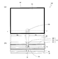
- FIG. 10A and 10B are diagrams showing an electronic apparatus 400 according to the fourth embodiment.
- FIG. 10A is a plan view when viewed from the observer side
- FIG. 10B is an xx in FIG. 10A. It is sectional drawing along a line.
- a hole 10A is provided in the display panel 10
- input devices 34 and 38 are provided at positions corresponding to the hole 10A.
- the input devices 34 and 38 are connected to the circuit board 20.
- the same referential mark is attached
- the electronic device 400 includes, as input devices 34 and 38, a camera module 34 and a fiber optic face plate (FOP) 38 provided on the viewer side of the camera module 34.
- FOP fiber optic face plate
- the camera module 34 is disposed inside the hole 10 ⁇ / b> A of the display panel 10.
- the fiber optic face plate 38 is disposed at a position protruding from the observer-side surface of the display panel 10.
- the electronic device 400 includes a touch panel 50 and a translucent cover 52.
- the touch panel 50 and the translucent cover 52 are provided with holes at positions corresponding to the holes 10A of the display panel.
- the fiber optic face plate 38 is disposed inside a hole provided in the touch panel 50 and the translucent cover 52. Thereby, since the observer side surface of the apparatus 400 can be made flat, it can improve appearance.
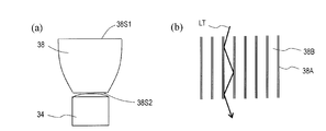
- FIG. 11A shows the fiber optic face plate 38 and the camera module 34.
- the fiber optic face plate 38 has a tapered shape. More specifically, the fiber optic face plate 38 has a shape in which the area of the end surface 38S1 on the viewer side is larger than the area of the end surface 38S2 on the camera module 34 side.
- the camera module 34 is accommodated in the hole 10 ⁇ / b> A of the display panel 10, while the fiber optic face plate 38 disposed outside the display panel 10 is not displayed.
- the region RF2 can be hidden.
- the fiber optic face plate 38 is formed by bundling a plurality of optical fibers each having a core layer 38A and a clad layer 38B provided outside the core layer 38A.
- the clad layer 38B has a refractive index lower than that of the core layer 38A, and the light LT incident from the viewer side end face 38S1 exceeding the critical angle repeatedly reflects at the interface while being reflected by the core. The light propagates through the layer 38A and is emitted from the end face 38S2 on the camera module 34 side. Accordingly, external light is incident on the camera module 34 via the fiber optic face plate 38.
- the diameter of the optical fiber gently changes along the thickness direction of the face plate. With such a configuration, light can be propagated in an enlarged / reduced manner without being attenuated.
- a tapered fiber plate is described in, for example, Japanese Patent Application Laid-Open No. 8-338916.
- the input device 30 may include a detachable part.
- the input device 30 may be configured by an operation unit that is disposed in the hole 10A of the display panel 10 and connected to the circuit board 20, and a stick unit that is detachable from the operation unit.
- a fitting hole or a screw hole is provided on the surface of the operation part, and the user inserts a stick part into the fitting hole or inserts a screw as necessary, thereby inputting an analog stick or other input device.
- a display panel having a display area and a frame area located outside the display area on the substrate, wherein a hole penetrating the substrate is provided inside the frame area;
- an input device including a portion protruding from the display panel on one side of the substrate; and an input device provided at a position corresponding to the hole;
- An electronic apparatus comprising a circuit board provided on the other side, wherein the input device is connected to the circuit board through the hole.
- the input device is provided at a position corresponding to the hole provided in the display area of the display panel, and the frame area can be narrowed without impairing the convenience for the user.
- the non-display area formed around the hole can be made inconspicuous.
- a separate wiring region having a wiring pattern different from other regions is formed around the hole, the non-display region includes the separate wiring region, and the input device at least partially includes the separate wiring region.
- the separate wiring area included in the non-display area formed around the hole can be made inconspicuous.
- the light-transmitting cover that covers at least a part of the display panel, and the light-transmitting cover includes a lens portion having a curved surface around the hole.
- Electronic equipment
- the non-display area formed around the hole can be made inconspicuous by the lens portion.
- Item 5 The electronic device according to Item 4, wherein the translucent cover covers at least a peripheral region of the hole of the display panel, and has another lens portion in a region corresponding to an end portion of the display panel.
- the display panel includes a pair of substrates including the substrate and a display medium layer held between the pair of substrates, and a non-display area formed around the hole between the pair of substrates. 6.
- the electronic device according to any one of items 1 to 5, wherein a seal portion for sealing the space is provided.
- the input device includes a first portion having a size larger than the hole and projecting from a viewer-side surface of the display panel, and a second portion connected to the first portion and disposed inside the hole.
- the electronic device according to any one of Items 1 to 6,
- a suitable input device that penetrates the hole is provided.
- An image processing unit configured to generate image data to be supplied to the display panel, the image processing unit configured to generate image data for displaying an image related to the input device around the input device;
- the electronic device according to any one of items 1 to 7.
- the display image can be linked to the operation of the input device, the convenience for the user can be further improved.
- the input device can be operated on the display screen.
- an input device that can be directly operated by the user is provided.
- an input device including a light receiving element is provided.
- Item 12 The electronic device according to Item 11, wherein the input device includes an image sensor and a fiber optic face plate disposed in front of the image sensor.
- a suitable imaging device is provided.
- the frame area can be narrowed without impairing user convenience.
- the electronic device according to the embodiment of the present invention is widely used in an electronic device including a display panel such as a portable game machine or a smartphone.
Landscapes
- Engineering & Computer Science (AREA)
- Physics & Mathematics (AREA)
- Computer Hardware Design (AREA)
- Theoretical Computer Science (AREA)
- General Physics & Mathematics (AREA)
- Nonlinear Science (AREA)
- General Engineering & Computer Science (AREA)
- Human Computer Interaction (AREA)
- Crystallography & Structural Chemistry (AREA)
- Chemical & Material Sciences (AREA)
- Optics & Photonics (AREA)
- Mathematical Physics (AREA)
- Devices For Indicating Variable Information By Combining Individual Elements (AREA)
Abstract
電子機器(100)は、基板上において表示領域(RA)と表示領域の外側に位置する額縁領域(RF)とが設けられた表示パネル(10)であって、額縁領域(RF)の内側において基板を貫通する孔(10A)が設けられ、孔の周囲に非表示領域(RF2)が形成されている表示パネル(10)と、基板の一方の側において、孔(10A)に対応する位置に設けられた入力デバイス(30)と、基板の他方の側に設けられた回路基板(20)とを備え、入力デバイス(20)は、孔(10A)を通って回路基板(20)と接続されている。
Description
本発明は、表示パネルを備える電子機器に関する。
一般に、透過型の液晶表示装置は、液晶パネル、バックライト装置、液晶パネルに各種の電気信号を供給するための回路基板や電源、および、これらを収容する筐体などを備えている。
液晶パネルには、複数の画素が配列された表示領域(アクティブエリア)と、その外側に位置する額縁領域(非アクティブエリア)とが設けられている。表示領域には、画素電極やTFTなどが設けられており、画像や映像が表示される。一方、額縁領域には、液晶材料を基板間に封止するためのシール部、走査線または信号線に接続された配線やモノリシックに形成された駆動回路、外部の駆動回路に接続される端子などが配置されており、画像や映像の表示に用いられない。
液晶パネルの額縁領域は、表示に寄与しない領域であるので、狭小化されることが好ましい。しかし、液晶パネルの狭額縁化が年々進んではいるものの、額縁領域を無くすことは原理的に困難である。
従来から、表示パネルに設けられた額縁領域を狭小化する、あるいは、目立たなくする方法が検討されている。本出願人は、特許文献1において、表示パネルの観察者側に透光性カバーを設ける表示装置を開示している。この表示装置において、透光性カバーの端部には、レンズとして機能する凸曲面部分が設けられている。
透光性カバーの凸曲面部分(レンズ部)は、典型的には、表示パネルの額縁領域と、額縁領域近傍の表示領域の一部(以下、周辺表示領域と呼ぶ場合がある)とを覆うように配置される。周辺表示領域に配列された画素(周辺画素)から出射された光は、レンズ部において屈折し、その結果、周辺画素が形成する画像が、額縁領域の前方に拡大されて表示される。これにより、観察者には、額物領域上にも画像が存在するように見えるので、額縁領域が目立ちにくくなる、あるいは、額縁領域が存在しないように見える。
なお、このような額縁領域を目立たなくするという課題は、液晶表示装置だけではなく、有機EL表示装置や、電気泳動方式の表示装置などにおいても同様に存在するものである。
上記のような表示装置を用いれば、例えば携帯型の電子機器(スマートフォンなど)において、電子機器の観察者側パネル面の略全域を表示可能領域として提供することが可能になる。このような電子機器は、機器のサイズに対して、情報表示が可能な領域が大きいので、機器の小型化という観点から有利である。また、近未来的なスタイリッシュさを呈する電子機器として、広く人々の感興をそそるものと思われる。
上記のように、表示パネルを備えた電子機器において、電子機器の観察者側パネル面(パネル前面)の全体を表示に利用する試みが為されている。ただし、電子機器の用途によっては、ユーザからの入力を受け取るための物理的・電気的なスイッチ(ボタン)や、カメラ・光学センサなどの光学デバイス、マイクロフォンなど音声デバイスを機器の表面に設けることが好ましいことがある。ボタンやカメラは、従来の電子機器では、表示パネルの額縁領域など、表示パネルの外側に配置されていた。したがって、上記のように額縁領域を無くすように設計された電子機器では、ボタンなどをどのように配置するかが問題になる。
額縁領域の狭小化を優先させるのであれば、電子機器の前面ではなく、例えばその背面や側面において、ボタンスイッチを設けることが考えられる。あるいは、観察者側のパネル面全体にタッチパネルを配置し、ボタンスイッチに代わる機能をタッチパネルに担わせることによって、物理的なスイッチをパネル前面から排除する構成も考えられる。このようにすれば、最大面積の表示領域を得ることが可能である。
しかし、本発明者による検討の結果、上記のような構成では、ユーザの利便性が十分でない場合があることがわかった。また、従来のようにボタンスイッチやカメラなどの装置を額縁領域に配置する構成では、電子機器のパネル面上により広い表示可能領域を設けることが困難であった。また、カメラなどでは、表示領域とカメラの位置とがずれていると、特にテレビ電話を行う場合などで、目線が合わず使いづらいといった課題があった。
本発明は、上記課題を解決するためになされたものであり、表示パネルを備える電子機器において、ユーザの利便性を損ねることなく、パネル前面における表示利用可能な領域を拡大させ得る電子機器を提供することをその目的とする。
本発明の実施形態による電子機器は、基板を有し、前記基板上において表示領域と前記表示領域の外側に位置する額縁領域とが設けられた表示パネルであって、前記額縁領域の内側において前記基板を貫通する孔が設けられ、前記孔の周囲に非表示領域が形成されている表示パネルと、前記基板の一方の側において前記表示パネルから突出する部分を含み、前記孔に対応する位置に設けられた入力デバイスと、前記基板の他方の側に設けられた回路基板とを備え、前記入力デバイスは、前記孔を通って前記回路基板と接続されている。
ある実施形態において、前記入力デバイスは、前記孔の周囲に形成された前記非表示領域を少なくとも部分的に覆う。
ある実施形態において、前記孔の周囲には、配線パターンが他の領域とは異なる別配線領域が形成されており、前記非表示領域は前記別配線領域を含み、前記入力デバイスは前記別配線領域を少なくとも部分的に覆う。
ある実施形態において、上記の電子機器は前記表示パネルの少なくとも一部を覆う透光性カバーを備え、透光性カバーは、前記孔の周囲に、曲面の表面を有するレンズ部を有している。
ある実施形態において、前記透光性カバーは、前記表示パネルの前記孔の周辺領域を少なくとも覆い、前記表示パネルの端部に対応する領域に、別のレンズ部分を有している。
ある実施形態において、前記表示パネルは、前記基板を含む一対の基板と、前記一対の基板間に保持される表示媒体層とを有し、前記孔の周囲に形成された非表示領域に、前記一対の基板間の空間を封止するためのシール部が設けられている。
ある実施形態において、前記入力デバイスは、前記孔よりも大きいサイズを有し前記表示パネルの観察者側表面から突出する第1部分と、前記第1部分と連結され前記孔の内部に配置される第2部分とを有する。
ある実施形態において、前記表示パネルに供給する画像データを生成する画像処理部を有し、前記画像処理部は、前記入力デバイスの周囲において前記入力デバイスに関連する画像を表示させるための画像データを生成可能に構成されている。
ある実施形態において、前記入力デバイスに関連する画像は、前記入力デバイスを操作するための画像である。
ある実施形態において、前記入力デバイスは、ユーザが直接操作することができるように構成されており、前記ユーザの操作に応じて前記回路基板に信号が供給される。
ある実施形態において、前記入力デバイスは、受光素子を含む。
ある実施形態において、前記入力デバイスは、撮像素子と、前記撮像素子の前段に配置されたファイバオプティックフェイスプレートを含む。
ある実施形態において、前記ファイバオプティックフェイスプレートはテーパ型であり、前記表示パネルの観察者側の端面の面積が、他方の端面の面積よりも大きい。
ある実施形態において、前記表示パネルは、液晶表示パネルである。
本発明の実施形態による電子機器によれば、ユーザの利便性を低下させることなく、機器のサイズに対して比較的大きい表示可能領域を得ることができる。
まず、本発明の実施形態による電子機器の概要を説明する。
本発明者は、狭額縁の表示パネルを備える電子機器において、ボタンスイッチや、カメラなどの入力デバイスの配置について鋭意検討した。その結果、これらの入力デバイスを、額縁領域などではなく、敢えて、表示パネルの表示領域内に配置することによって、ユーザの利便性を損なうことなく表示可能領域を拡大することができ、また、この拡大された表示可能領域を有効に利用できるとの結論を得た。表示領域内に入力デバイスを配置する構成によれば、電子機器のパネル前面の全周縁にまでも、画像を表示することが可能になる。
上記の入力デバイスとしては、例えば、携帯型ゲーム機の操作ボタン(十字キーなど)が挙げられる。このような操作ボタンは、ユーザの操作性を考慮すると、機器の観察者側表面(パネル前面)に配置されていることが好ましい。操作ボタンを他の箇所に設けたり、あるいは、タッチパネル上でソフトウェアによって再現した場合、ユーザの操作性は著しく低下する。また、操作ボタンに限られず、ユーザの顔などを映すための前面カメラは、テレビ電話などで画面を使用する都合上、パネル前面に設けることが求められている。
ここで、表示パネルの表示領域には、液晶層や発光ダイオードなどが配置され、複数の画素が設けられている。例えば、液晶パネルの場合、額縁領域に配置されたシール部によって封止された空間内に液晶層が保持されており、表示領域は、この液晶層が封止された空間において設けられている。
従来、表示パネルの表示領域において、上記のような入力デバイスを設けることは、行われていなかった。その理由は、入力デバイスは、液晶パネルの背面側に配置される回路基板などと接続されることが多く、入力デバイスを表示領域内に配置することは製造上の大きな困難性を伴うと考えられていたからである。また、従来の電子機器では、ある程度の面積を有する額縁領域が設けられていることが通常であったので、敢えて、表示領域内に入力デバイスを配置する必要性がなかった。
これに対して、本発明者の検討の結果、表示パネルの表示領域(従来の額縁領域の内側)に表示パネルを貫通する孔を空けることは実現可能であり、この孔を通して、入力デバイスを表示パネル背面の回路基板に接続することによって、ユーザの利便性を損なわずに表示領域を拡大し得ることがわかった。
例えば、液晶パネルにおいて孔を設ける場合、パネル周縁だけでなく孔の周囲においてもシール材を配置し、基板を貼り合わせた後に孔を形成することによって、他の領域に大きな影響を与えることなく液晶パネルを作製することが可能である。なお、液晶層の形成は、例えば、パネル周縁や孔周囲にシール材を配置した後、基板貼り合わせ前の段階で片側の基板上に液晶を滴下し、その後、基板を貼り合わせすることによって行うことができる。あるいは、上記のようにパネル周縁や孔の周囲にシール材を配置し、基板を貼り合わせた後に、液晶を注入する工程によって液晶層を形成することもできる。
また、表示パネルにおいて、一般的には、画素を駆動するための導電パターンが配列されている。しかし、孔を設ける場合、孔の周辺では他の領域と同様に配線を行うことが困難になる。しかしながら、例えば、孔を避けるようにして配線を行うことは可能であり、孔およびその周辺を除く他の領域では、適切に画像などを表示させることができる。
ただし、上記のように、液晶パネルに孔を設ける場合、孔の周りには液晶を封止するためのシール材が設けられる。これによって、孔の周りにおいても非表示領域が形成される。しかし、このような非表示領域を、入力デバイスによって覆うようにすれば、孔周辺を目立たなくすることができる。これによって、装置としての一体感が得られる。
また、入力デバイスで覆う以外にも、表示パネルの観察者側に透光性カバーを設け、孔の周囲において透光性カバーにレンズ部を設けてもよい。これにより、孔周辺の非表示領域を目立たなくすることができる。
なお、表示領域内に孔が設けられた液晶パネルは、例えば、特許文献2~4に開示されている。ただし、特許文献2~4に記載の表示装置は、この孔に、入力デバイスを配置する構成を開示するものではない。また、孔の周囲を目立たなくし、入力デバイスと表示パネルとの一体感を提供できる構成を開示するものではない。
以下に説明する本発明の実施形態において、電子機器に設けられる入力デバイスは、ユーザからの入力を受け取る物理的・電気的なスイッチ、ボタンや、外光を受光することができる光学素子など、種々のデバイスであってよい。
より具体的には、入力デバイスは、ユーザからの入力(直接操作)を受け取る、押しボタン、方向キー(十字キー)、アナログスティック、タッチパネル、ロータリスイッチ(ボリュームコントローラ)、回転式セレクタ(ジョグダイヤル)、トグルスイッチ、トラックボール、トラックパッド、スティック型ポインティングデバイス、ハードウェアキーボードなどを含む。
また、入力デバイスは、光学的な入力を受け取る、撮像素子(CCDイメージセンサ、CMOSイメージセンサなど)、受光素子(ファイバオプティックフェイスプレートなど)、光学センサなどを含む。その他、温度センサ、マイクロフォン、HDMI(登録商標)やUSBなどの入力端子、プラグやコンセントなどの配線端子などであってもよい。
これらの入力デバイスは、表示パネルの背面側に配置される回路基板に対して、物理的、電気的あるいは光学的に接続されている。入力デバイスからの入力は、回路基板において処理されてよい。このような構成によって、パネル面における表示可能な領域を増大させながら、ユーザの利便性を確保することができる。
本発明の実施形態による電子機器は、種々の電子機器であってよく、例えば、携帯型ゲーム機、スマートフォン、モバイルフォン、PDA、タブレット型端末、電子ブックリーダー、音楽プレーヤー、カメラ、電子辞書、電子ノート、ナビゲーションシステム、表示装置、パーソナルコンピュータ、ウェアラブルコンピュータ、遊戯機、テレビジョン、インフォメーションディスプレイなどであってよい。
以下、図面を参照しながら本発明の実施形態を説明するが、本発明は以下の実施形態に限られるものではない。
(実施形態1)
図1は、実施形態1の電子機器100の構成を示す図であり、図1(a)はユーザから見たときの平面図、図1(b)は図1(a)のx-x’線に沿った断面図である。また、図3は、電子機器100において、表示パネル10に設けられた孔10Aの近傍の領域を拡大して示す断面図である。
図1は、実施形態1の電子機器100の構成を示す図であり、図1(a)はユーザから見たときの平面図、図1(b)は図1(a)のx-x’線に沿った断面図である。また、図3は、電子機器100において、表示パネル10に設けられた孔10Aの近傍の領域を拡大して示す断面図である。
実施形態1の電子機器100は、液晶パネル(表示パネル)10と、液晶パネル10の背面側(観察者側とは反対側)に配置された回路基板20とを備えている。また、本形態の液晶パネル10は透過型であり、液晶パネル10と回路基板20との間にはバックライト40が設けられている。バックライト40は、LEDなどの光源に加え、導光板、拡散板、反射板などの光学素子を備えるエッジライト型のバックライトであってもよいし、直下型(面発光型)のバックライトであってもよい。
液晶パネル10は、TFT基板11と、これに対向する対向基板12と、これらの一対の基板間に保持される液晶層14とを備えている。液晶層14は、周辺額縁領域RFに設けられたシール部13や、後述する孔10A周りのシール部13’によって、基板11、12の間に封止されている。
なお、図3に示すように、TFT基板11は、透明基板11’上に、画素電極(透明電極)16などが設けられた構成を有する。また、対向基板12は、透明基板12’上に、共通電極(透明電極)17やカラーフィルタ18などが設けられた構成を有する。また、TFT基板11と対向基板12の外側面には、偏光板や位相差フィルムなどからなる、光学フィルム層15が粘着層を介して貼られている。ただし、これらは例示的なものであり、液晶パネル10は種々の公知の構成を有し得る。
再び図1を参照する。液晶パネル10には、画素が配列されている表示領域(アクティブエリア)RAと、その外側に設けられた額縁領域RF(以下、周辺額縁領域RFと呼ぶことがある)とが設けられている。なお、ここでは、液晶パネル10の周辺に形成された額縁領域RFの内側の領域を、便宜上、表示領域RAと呼んでいる。表示領域RAには、表示に寄与しない領域が含まれていても良い。
電子機器100において、液晶パネル10の周辺額縁領域RFの内側(すなわち表示領域RA内)には、液晶パネル10を貫通する孔10Aが設けられている。また、孔10Aの周囲には、非表示領域RF2が形成されている。孔10Aは、TFT基板11、対向基板12、液晶層14などを貫通している。さらに、孔10Aは、バックライト40をも貫通している。
なお、孔10Aの直径は、適宜選択されて良いが、例えば、1mm~15mmに設定される。また、ここでは、孔10Aの平面形状が円形である場合を例示しているが、四角形など他の任意の平面形状を有していても良い。
孔10Aは、表示領域RA内に配置されているが、画素が配列されていないので、表示に寄与する領域ではない。また、孔10Aの周囲には、シール部13’やブラックマトリクス(図示せず)を含む環状の非表示領域RF2が形成されている。この非表示領域RF2も、額縁領域RFの内側の領域として規定される表示領域(アクティブエリア)RA内に配置されているが、表示に寄与する領域ではない。
また、電子機器100には、表示領域RA内に設けられた孔10Aを通るように配置された、入力デバイス30が設けられている。入力デバイス30は、本実施形態では、押下型の電気スイッチであり、例えば、スマートフォンに設けられたハードウェアボタンがこれに該当する。
以下、入力デバイス30についてより詳細に説明する。
電子機器100において、入力デバイス30は、液晶パネル10の観察者側表面より突出した部分である前面部(スイッチキャップ)30Aと、前面部30Aに連結され、液晶パネル10の孔10Aの内部に配置された延長部30Bとを有している。また、入力デバイス30は、回路基板20上に設けられたコネクタ部30Cを有している。このような構成において、入力デバイス30は、コネクタ部30Cによって回路基板20に接続されている。
入力デバイス30のうち、ユーザ側(観察者側)に配置される前面部30Aは、孔10Aの口径よりも大きい径を有する拡幅部分として設けられている。前面部30Aは、孔10A、および、孔10Aの周囲に設けられた非表示領域RF2を覆っている。
入力デバイス30は、孔10Aの口径よりも大きい径を有する拡幅部分を有しているので、前記のように前面部30Aと延長部30Bが連結されている構成でないと、回路基板に実装しづらい場合がある。連結されている構成である場合、回路基板に延長部30Bを実装した後に、これを液晶パネルの孔10Aを貫通させてから前面部30Aをはめ込むことで、容易に組み立てが可能になる。
図3は、前面部30Aの近傍を拡大して示す。図3に示すように、液晶パネル10において、孔10Aの周囲に存在する非表示領域RF2は、孔周囲のシール部13’と、光漏れを防ぐための遮光領域(ブラックマトリクス)13Bとを含んでいる。遮光領域13Bは、黒色樹脂などで形成されているので、目立ちやすい。したがって、前面部30Aは、シール部13’や遮光領域13Bを含む非表示領域RF2をユーザから隠すように形成されていることが好ましい。
本実施形態において、前面部30Aは、非表示領域RF2から距離(公差)dだけ外側の領域までを覆うように形成されている。これは、製造工程において、非表示領域RF2と前面部30Aとの位置ずれが生じたり、前面部30Aの寸法ずれが生じた場合にも、非表示領域RF2を前面部30Aによって覆うことをより確実にできるからである。距離dは、例えば0.1mm程度に設定される。なお、非表示領域RF2は、厳密には、孔10Aを挟んで対向配置された画素電極16間の領域として規定される。
TFT基板11には、TFT(図示せず)、画素電極16などを含むマトリクス駆動回路が形成されている。一方、対向基板12には、共通電極17やカラーフィルタ18などが形成されている。本実施例の液晶パネル10には孔10Aが空けられており、例えば、特許文献3に示されるように、孔10Aの周辺のマトリクス配線が孔10Aを避けるように形成されていてよい。
このようにして、孔10Aの周りに配線が迂回して形成されている場合、配線ピッチが詰まって配されることがある。また、この周辺では、開口率が低下していることがある。したがって、前面部30Aは、配線の詰まった領域(別配線領域と呼ぶことがある)の少なくとも一部を覆うように設けられていてもよい。これにより、表示に利用しにくい領域をまとめて前面部30Aによって目立たなくすることができる。
図12(a)は、孔10Aの周りにおけるTFT基板上の配線の一例を示す。図示するように、孔10Aの周囲において、垂直方向に延びるソース配線4、および、これと直交する水平方向に延びるゲート配線2との双方が、孔10Aを迂回するように設けられている。この構成において、孔10Aの周辺以外の領域ではマトリクス状に画素を設けることができ、ソース配線4やゲート配線2を用いてTFT(図示せず)に接続された画素電極16(図参照)に所定の電圧を印加し、画像などを表示することができる。なお、TFTは、In-Ga-Zn-O系半導体層などの酸化物半導体層からチャネルが形成されるものであってもよい。
ただし、図12(a)に示すように、孔10Aの周囲には、迂回する配線を含む別配線領域RF3が設けられる。別配線領域RF3は、開口率が低く、画素を配置することが困難な領域である。別配線領域RF3は、表示に用いることができないので、ブラックマトリクスで覆っていても良い。
また、図12(b)に示すように、本実施形態の電子機器100では、別配線領域RF3を、入力デバイス30の前面部30Aで覆っている。これにより、ユーザから別配線領域RF3を隠すことができるので、前面部30Aと表示領域RAとの一体感のある構成をユーザに提供することができる。
このようにして、前面部30Aによって非表示領域RF2や別配線領域を隠すようにすれば、ユーザは、孔近傍において前面部30Aの表面RA’(図1参照)を見ることになり、非表示領域RF2を見ることがない。したがって、表示領域RAに配置された入力デバイス30が、表示パネル10と一体感を持つように感じられる。
図2は、比較形態の電子機器900の構成を示す図であり、図2(a)は観察者側から見たときの平面図であり、図2(b)は図2(a)に示すx-x’線に沿った断面図である。なお、図1に示す電子機器900と同様の構成要素には同じ参照符号を付すとともに説明を省略する。
図2(b)に示すように、電子機器900が備える液晶パネル10においても、孔10Aおよびその周囲に環状に形成された非表示領域RF2が形成されている。ここで、非表示領域RF2が観察者に視認される状態であると、この部分が目立つことになる。このため、実施形態1の電子機器100に比べると、入力デバイスと表示パネルとの一体感が損なわれることになる。
特に、非表示領域RF2の幅が、周辺額縁領域RFの幅よりも太い場合、非表示領域RF2は目立ちやすいので隠すことが好ましい。なお、非表示領域RF2の幅がより太くなる原因は、孔10Aの周辺では、孔を迂回するように配線を形成するため画素を設けることが困難であり、これをブラックマトリクスによって覆うこともあるからである。
再び、実施形態1の電子機器100を説明する。
図4(a)は、ユーザによる入力デバイス30の使用状況を説明するための図であり、ここでは、入力デバイスとして押しボタン式スイッチ30が用いられている場合を示す。ユーザは、表示領域RA内に配置されたボタン(スイッチ30の前面部30A)を押す操作を行うことができる。このボタン30Aの押下により、回路基板20上に配置されたコネクタ部30Cにおいて電気接点が接続することなどによって、入力(ボタンの押下)が行われたことを判断することができる。なお、押しボタン式のスイッチの構成については、公知の構成を利用することができるので、ここでは詳細に説明しない。
図4(b)は、ロータリスイッチ32である入力デバイスの使用状態を示す図である。ユーザは、表示領域内に配置され、孔10Aを通って回路基板20に接続されたロータリスイッチ32を回転させる操作を行うことができる。このスイッチの回転操作は、回路基板20上に配置されたコネクタ部において電気信号として受け取られてよい。なお、ロータリスイッチ32の構成については、公知の構成を利用することができるので、ここでは詳細に説明しない。
以下、表示パネルの表示領域内(例えば、孔および入力デバイスの周囲)において、入力デバイスに関連した画像を表示する形態について説明する。
図5(a)~(c)は、表示領域RA内に、入力デバイスとしてのロータリスイッチ32が設けられている様子を示す。
図5(a)および(b)に示すように、本発明の実施形態による電子機器は、表示領域RAにおいて、ロータリスイッチ32に関連する画像や情報を表示するように構成されていてもよい。例えば、ロータリスイッチ32がボリュームコントローラとして機能する場合、ユーザによるロータリスイッチ32の操作に応じて、現在のボリュームの大きさをロータリスイッチ32の周囲に表示するように、電子機器が構成されていてもよい。
このように、入力デバイスに関連する画像を表示することで、入力デバイスと表示パネルとが一体的に動作しているような体験をユーザに提供し得る。また、入力デバイスの操作に応じて、ユーザが必要とする情報を適宜変更して表示することによって、ユーザの利便性を高めることができる。さらに、現在の入力デバイスの機能がどのようなものであるかを、表示パネル上の画像によってユーザに認識させることが可能であるので、入力デバイスを多目的に使用しやすいという利点も得られる。
図5(c)は、比較形態の電子機器を示す。この電子機器では、表示パネルから突出するロータリスイッチが、孔の周囲に形成される非表示領域RF2を覆っていない様子を示している。この場合、表示領域RAに表示される表示画像と、スイッチとの間に非表示領域RF2がユーザに観察される。このため、図5(a)および(b)に示す形態に比べて、ユーザが直観的な操作を行いにくい。また、スイッチと画像との一体感が薄れることになる。
なお、上記のように、表示パネルにおいて、入力デバイスに関連する画像を入力デバイスの周囲に表示するために、公知の画像処理装置(画像処理部)などを用いることができる。画像処理装置は、例えば、回路基板上に設けられた演算処理ユニットやグラフィック処理ユニットなどを含んでいて良い。画像処理装置は、表示パネルに表示する画像を決定する画像データを生成することができるように構成されており、これを適切に制御することによって、入力デバイスの周囲に関連画像を表示させることができる。
図6(a)および(b)は、変形例の電子機器102、104を示す。これらの電子機器102、104において、表示パネル10の観察者側には、タッチパネル50および透光性カバー(前面板)52が設けられている。タッチパネル50は公知の構成を有していて良い。また、透光性カバー52は、典型的には透光性のガラスや樹脂材料から形成されている。なお、透光性カバー52とタッチパネル50とは、一体的に形成されていても良い。
図6(a)に示す電子機器102において、入力デバイス30の前面部30Aは、表示パネル10のユーザ側表面から突出している。ただし、前面部30Aの表面は、透光性カバー52の表面と略同じレベルの位置に存在している。このような配置によれば、電子機器102のユーザ側表面において凹凸が形成されにくいので見栄えがよい。また、入力デバイス30が押しボタンである場合などに、不用意にスイッチを押してしまう可能性を低減できる。このように、透光性カバー52の最前面をフラットにできる構成は、デザイン上好ましく、特に携帯電話やスマートフォン、タブレットなどの薄型が特に重視される電子機器において好適である。
また、図6(b)に示す電子機器104において、入力デバイス30の前面部30Aは、表示パネル10のユーザ側表面だけでなく、タッチパネル50および透光性カバー52の表面からも突出している。入力デバイス30がロータリスイッチなどの場合には、このような構成である方がユーザの操作性が向上する。
以上のいずれの場合においても、入力デバイス30の前面部30Aは、孔10Aの周囲の非表示領域RF2を覆っていることが好ましい。これにより、孔10Aを目立ちにくくすることができ、入力デバイス30と表示パネル10との一体感が得られる。
なお、図6(a)および(b)に示すように、入力デバイス30を設ける場合、典型的には、タッチパネル50および透光性カバー52においても、対応する位置に孔が設けられる。ただし、後述するように、入力デバイス30が受光素子のように、ユーザの直接入力を必要としないデバイスである場合、タッチパネル50および透光性カバー52は、孔を有しておらず、入力デバイス30の前面部30Aを覆っていても良い。
また、図6(a)および(b)には、表示パネル10の観察者側にアウトセル型のタッチパネル50が設けられた形態を示しているが、本発明の実施形態は、このような形態に限られない。アウトセル型のタッチパネル50に代えて、オンセル型、インセル型のタッチパネルを用いることもできる。インセル型のタッチパネルを用いる場合、表示パネル10の内部においてタッチパネルが構成される。
以上に説明したように、本実施形態の電子機器では、スイッチなどの入力デバイスによって、表示パネルに存在する非表示領域(例えば、シール部、画素電極が形成されない領域、および、部品と表示パネルとの隙間を含む領域)を隠すことができるので、表示画面の中にスイッチが違和感無く溶け込むデザインが実現できる。また、スイッチ操作と画像を連動させることによって、ユーザの使い勝手が格段によくなるという利点や、少ないスイッチで多彩な操作が可能になるという利点が得られる。
(実施形態2)
図7(a)は、実施形態2の電子機器200を示す断面図である。また、図7(b)および(c)は、それぞれ別の変形例202、204を示す断面図である。実施形態2の電子機器200、202、204では、実施形態1の電子機器100とは異なり、入力デバイスとして光学デバイスを備えている。なお、実施形態1と同様の構成要素には同じ参照符号を付すとともに説明を省略する。
図7(a)は、実施形態2の電子機器200を示す断面図である。また、図7(b)および(c)は、それぞれ別の変形例202、204を示す断面図である。実施形態2の電子機器200、202、204では、実施形態1の電子機器100とは異なり、入力デバイスとして光学デバイスを備えている。なお、実施形態1と同様の構成要素には同じ参照符号を付すとともに説明を省略する。
図7(a)に示す電子機器200は、表示パネル10、バックライト40、回路基板20を備えている。表示パネル10の表示領域には、実施形態1の電子機器100と同様に、基板を貫通する孔10Aが設けられている。
電子機器200では、孔10Aに対応する位置において、カメラモジュール(撮像素子)34が配置されている。カメラモジュール34は、表示パネル10の観察者側表面から突出するようにして、表示パネル10に形成される孔周りの非表示領域RF2を覆うように配置されている。カメラモジュール34は、表示パネル10の上面に飛び出していた方が、光などを取り込みやすくなるために、感度を向上させることができたり、画角を広げられる点で好ましい。
電子機器200において、図6(a)および(b)に示した形態と同様に、タッチパネル50および透光性カバー52が、表示パネル10の観察者側に配置されている。また、孔10Aおよびカメラモジュール34に対応する位置において、タッチパネル50および透光性カバー52には孔が設けられている。この孔において、カメラモジュール34が露出している。
ただし、タッチパネル50および透光性カバー52が十分な透光性を有している場合などにおいて、図7(b)に示すように、電子機器202が備えるタッチパネル50および透光性カバー52は、孔を有さず、カメラモジュール34を覆うように設けられていてもよい。
また、図7(c)に示すように、電子機器204は、入力デバイスとして、カメラモジュールに限らず、種々の光学センサを有していても良い。光学センサは、照度センサや近接センサなどであり得る。照度センサは、周囲の明るさを認識して画面輝度の調整などに使用するために用いられる。また、近接センサは、近くに物体があるかどうかを判別するために用いられる。
図7(a)~(c)に示す電子機器200、202、204のように、カメラモジュール34や光学センサ36を備える場合においても、非表示領域RF2を、表示パネル前面に配置される入力デバイス34、36によって覆うことによって、孔10Aを目立たなくすることができる。これによって、一体感が損なわれない電子機器を提供することができる。
また、本実施形態においても、入力デバイス(光学デバイス)34、36は、表示パネル10の背面側に配置された回路基板20にコネクタ部を介して接続されている。回路基板20は、光学デバイス34、36からの入力信号に基づいて、画像データや照度データを生成できるように構成されていてよい。
なお、本実施形態の電子機器200、202、204においても、表示パネル10において、入力デバイスに関連する画像を表示してもよい。例えば、カメラモジュール34を備える場合、カメラモジュール34のすぐ近辺にカメラ起動ボタン等を表示し、その表示部分をタッチパネルで触れることによってカメラが起動するようなソフトウェアが実装されていてもよい。この場合、カメラモジュールと表示画像との連動により、ユーザがより直感的に操作できるために好ましい。また、カメラモジュール上にもタッチパネルを設ける場合には、カメラモジュール上を触れることでカメラが起動するソフトウェアとしてもよく、これにより、カメラモジュールとタッチパネルの連動性が得られる。
同様に、照度センサの調整なども、表示パネルに表示する画像と連携して操作できると好ましい。例えば、タッチパネル上の照度センサ付近の領域をユーザが触れることによって画面輝度調整をするように構成されていてよい。
なお、タッチパネルの電極による光の散乱等が、カメラモジュールやセンサ類に悪影響を与える可能性がある場合、カメラやセンサ類の上に対応する領域には、電極等を配置しないように設計しても良い。
(実施形態3)
図8は、実施形態3の電子機器300を示す図であり、図8(a)はユーザ側から見たときの平面図、図8(b)は、図8(a)のx-x’線に沿った断面図である。
図8は、実施形態3の電子機器300を示す図であり、図8(a)はユーザ側から見たときの平面図、図8(b)は、図8(a)のx-x’線に沿った断面図である。
図8(a)および(b)に示すように、電子機器300においても、表示パネル10に孔10Aが設けられ、孔10Aに対応する位置には入力デバイス30(ここでは押しボタン型スイッチ)が設けられている。入力デバイス30は、回路基板20と接続されている。なお、実施形態1と同様の構成要素には同じ参照符号を付すとともに説明を省略する。
電子機器300では、表示パネル10の観察者側に、透光性カバー60が設けられている。透光性カバー60は、ガラスやプラスチックなどの透光性の材料から形成されており、表示パネル10からの光を観察者側に透過させることが可能である。
また、透光性カバー60は、表示パネル10の孔10Aに対応する位置において、孔を有している。また、表示パネル10の孔10Aの周囲において、透光性カバー60は、表面が曲面の部分を有している。この曲面部分は、レンズ部60Bとして機能する。なお、レンズ部60Bの周りには平坦部60Aが設けられており、表示パネル10の大部分は平坦部60Aによって覆われている。ただし、表示パネル10の外周縁(額縁領域RFが形成されている領域)に対応して、透光性カバー60は、別のレンズ部(周辺レンズ部)60Cを有している。
図9は、孔10A近辺に設けられたレンズ部60Bの効果を説明するための図である。なお、図において、表示パネル10を通過して透光性カバー60の表面から出射される光の経路を破線で示している。図からわかるように、電子機器300では、透光性カバー60にレンズ部60Bが設けられているので、非表示領域RF2の近辺の画素領域から出射された光は、レンズ部60B(ここでは、レンズ部60Bのユーザ側表面)において屈折する。これにより、孔10Aの周辺に位置する画素が形成する画像が拡大されて、非表示領域上RF2の前面に表示される。したがって、孔10Aの周りにレンズ部60を配置するだけでも、非表示領域RF2を目立ちにくくすることができ、これによって、ユーザには入力デバイス30と表示パネル10とが一体性を有するように感じられる。
ここで、レンズ部60Bが有するレンズ曲面の形状(より具体的には、断面においてレンズ曲面が形成する曲線)は、曲率半径R1(または曲率c)と非球面係数(コーニック定数)kとを用いて例えば下記の式によって表わされる。
非球面式:f(x)=Y-cx2/(1+(1-(1+k)c2x2)1/2)
非球面式:f(x)=Y-cx2/(1+(1-(1+k)c2x2)1/2)
ただし、c=1/R1、xはレンズ頂上(レンズ部60Bと平坦部60Aとの境界)からの水平方向距離、Yはレンズ頂上における高さ(平坦部60Aにおける透光性カバー60の厚さ)である。曲率半径R1、コーニック定数k、透光性カバー60の厚さなどは、非表示領域RF2の幅などに応じて適宜設定されてよい。
より具体的なレンズ部60Bの形状については、国際公開第2009/157150号や、国際公開第2010/070871号において詳細に記載されている。本発明の実施形態においても、上記文献に記載のレンズ面形状を適用することができる。参考のために、国際公開第2009/157150号および国際公開第2010/070871号の開示内容の全てを本明細書に援用する。
また、孔10Aの周囲において、レンズ部60Bの形状は、例えば回転体の一部であることが好ましい。なお、回転体とは、平面図形をそれと同平面に位置する直線の周りに360°回転することにより得られる立体図形を意味する。本実施形態においてレンズ部60は、回転軸から離れた位置に設けられた平面図形であって、回転軸の側に曲線の線分を有する平面図形を回転させることによって得られる回転体を含む形状を有していてよい。
また、レンズ部の形状は、図9に示したような片側が凸レンズの形態に限られない。例えば、フレネルレンズを用いて形成されていても良い。また、観察者側表面と背面との双方が、凸曲面を有するように形成されていてもよい。また、レンズ部を有している限り、透光性カバーは種々の形態であってよい。例えば、透光性カバーは、孔10Aの周囲に設けられたレンズ部と、レンズ部から表示パネルの表面に向かって傾斜する傾斜部とを有し、孔10Aの周りのみを選択的に覆うような形態であってもよい。なお、本明細書では、このような孔10の周辺領域のみを選択的に覆うようなものであっても、「透光性カバー」と称する。
また、本実施形態の電子機器300では、周辺額縁領域RFに対して別のレンズ部60Cが設けられている。このため、孔10Aの周りに画像を表示させることができるのと同様に、表示パネル10の外周の周辺額縁領域RFにも画像を表示させることができる。したがって、入力デバイスが配置された領域以外の、電子機器300のパネル前面の全ての領域を、画像表示可能な領域として利用し得る。
なお、図8および図9に示す形態において、入力デバイス30の前面部30Aは、表示パネル10の孔周りに形成された非表示領域RF2を覆っていない点で実施形態1の電子機器100と異なる。ただし、本実施形態の電子機器のようにレンズ部を有する透光性カバーを設ける場合においても、入力デバイス30の前面部30Aが非表示領域RF2の一部または全部を覆っていてもよい。また、孔10Aの周辺の画素の配列ピッチを、中央画素の配列ピッチよりも小さく設定し、周辺画素からの光をレンズ部60Bで拡大するようにして表示を行っても良い。周辺画素の画素ピッチをより小さくする構成は、孔10A周りでの配線間隔を狭くする場合などに適合する。
(実施形態4)
図10は、実施形態4の電子機器400を示す図であり、図10(a)は観察者側から見たときの平面図、図10(b)は、図10(a)のx-x’線に沿った断面図である。電子機器400においても、表示パネル10に孔10Aが設けられ、孔10Aに対応する位置には入力デバイス34、38が設けられている。入力デバイス34、38は、回路基板20と接続されている。なお、実施形態1と同様の構成要素には同じ参照符号を付すとともに説明を省略する。
図10は、実施形態4の電子機器400を示す図であり、図10(a)は観察者側から見たときの平面図、図10(b)は、図10(a)のx-x’線に沿った断面図である。電子機器400においても、表示パネル10に孔10Aが設けられ、孔10Aに対応する位置には入力デバイス34、38が設けられている。入力デバイス34、38は、回路基板20と接続されている。なお、実施形態1と同様の構成要素には同じ参照符号を付すとともに説明を省略する。
電子機器400は、入力デバイス34、38として、カメラモジュール34と、カメラモジュール34の観察者側に設けられたファイバオプティックフェイスプレート(FOP)38とを含んでいる。
カメラモジュール34は、表示パネル10の孔10Aの内部に配置される。一方、ファイバオプティックフェイスプレート38は、表示パネル10の観察者側表面から突出した位置に配置されている。
また、電子機器400は、タッチパネル50および透光性カバー52を有している。タッチパネル50および透光性カバー52には、表示パネルの孔10Aに対応する位置に孔が設けられている。ファイバオプティックフェイスプレート38は、タッチパネル50および透光性カバー52に設けられた孔の内部に配置されている。これにより、機器400の観察者側表面を平らにすることができるので、見栄えを良くすることができる。
図11(a)は、ファイバオプティックフェイスプレート38とカメラモジュール34とを示している。図11(a)に示すように、ファイバオプティックフェイスプレート38は、テーパ型の形状を有している。より具体的には、ファイバオプティックフェイスプレート38は、カメラモジュール34側の端面38S2の面積よりも、観察者側の端面38S1の面積の方が大きい形状を有している。このようなテーパ型のファイバオプティックフェイスプレート38を用いることによって、表示パネル10の孔10A内にカメラモジュール34を収容しながら、表示パネル10の外側に配置されたファイバオプティックフェイスプレート38によって、非表示領域RF2を隠すことができる。
なお、図11(b)に示すようにファイバオプティックフェイスプレート38は、それぞれがコア層38Aとコア層38Aの外側に設けられるクラッド層38Bとを有する複数の光ファイバを束ねることで形成されている。典型的には、クラッド層38Bの屈折率は、コア層38Aの屈折率よりも低く形成されており、観察者側端面38S1から臨界角を超えて入射した光LTが界面で反射を繰り返しながらコア層38Aの内部を伝播し、カメラモジュール34側端面38S2から出射される。これにより、カメラモジュール34には、ファイバオプティックフェイスプレート38を介して外光が入射される。
テーパ型のファイバオプティックフェイスプレート38において、光ファイバの径がフェイスプレートの厚さ方向に沿ってなだらかに変化している。このような構成によって、光を減衰することなく拡大/縮小して伝播させることが出来る。テーパ型のファイバープレートは、例えば、特開平8-338916号公報に記載されている。
以上、本発明の実施形態を説明したが、種々の改変が可能であることは言うまでもない。例えば、上記には表示パネルとして液晶パネルを用いる例を説明したが、これに限られない。表示パネルとしては、有機ELディスプレイ、プラズマディスプレイパネル、電気泳動方式の表示パネル、エレクトロウェッティング方式の表示パネルなどを用いることができる。有機ELディスプレイなどの自発光型の表示パネルを用いる場合、バックライトを有していなくても良いことは言うまでもない。
また、上記の入力デバイス30は、着脱可能な部分を含んでいても良い。例えば、入力デバイス30は、表示パネル10の孔10A内に配置され回路基板20と接続される動作部と、動作部に対して着脱可能なスティック部とから構成されていてもよい。動作部の表面には、例えば、嵌合孔やネジ穴が設けられ、ユーザは、必要に応じて、この嵌合孔にスティック部を差し込んだりネジ入れたりすることにより、アナログスティックなどの入力デバイスとして利用することができる。
本明細書は、以下の項目に記載の電子機器を開示している。
[項目1]
基板を有し、前記基板上において表示領域と前記表示領域の外側に位置する額縁領域とが設けられた表示パネルであって、前記額縁領域の内側において前記基板を貫通する孔が設けられ、前記孔の周囲に非表示領域が形成されている表示パネルと、前記基板の一方の側において前記表示パネルから突出する部分を含み、前記孔に対応する位置に設けられた入力デバイスと、前記基板の他方の側に設けられた回路基板とを備え、前記入力デバイスは、前記孔を通って前記回路基板と接続されている、電子機器。
基板を有し、前記基板上において表示領域と前記表示領域の外側に位置する額縁領域とが設けられた表示パネルであって、前記額縁領域の内側において前記基板を貫通する孔が設けられ、前記孔の周囲に非表示領域が形成されている表示パネルと、前記基板の一方の側において前記表示パネルから突出する部分を含み、前記孔に対応する位置に設けられた入力デバイスと、前記基板の他方の側に設けられた回路基板とを備え、前記入力デバイスは、前記孔を通って前記回路基板と接続されている、電子機器。
項目1に記載の電子機器では、表示パネルの表示領域に設けられた孔に対応する位置に入力デバイスが設けられており、ユーザの利便性を損ねることなく、額縁領域を狭小化し得る。
[項目2]
前記入力デバイスは、前記孔の周囲に形成された前記非表示領域を少なくとも部分的に覆う、項目1に記載の電子機器。
前記入力デバイスは、前記孔の周囲に形成された前記非表示領域を少なくとも部分的に覆う、項目1に記載の電子機器。
項目2に記載の電子機器によれば、孔の周囲に形成された非表示領域を目立たなくすることができる。
[項目3]
前記孔の周囲には、配線パターンが他の領域とは異なる別配線領域が形成されており、前記非表示領域は前記別配線領域を含み、前記入力デバイスは前記別配線領域を少なくとも部分的に覆う、項目2に記載の電子機器。
前記孔の周囲には、配線パターンが他の領域とは異なる別配線領域が形成されており、前記非表示領域は前記別配線領域を含み、前記入力デバイスは前記別配線領域を少なくとも部分的に覆う、項目2に記載の電子機器。
項目3に記載の電子機器によれば、孔の周囲に形成された非表示領域に含まれる別配線領域を目立たなくすることができる。
[項目4]
前記表示パネルの少なくとも一部を覆う透光性カバーを備え、透光性カバーは、前記孔の周囲に、曲面の表面を有するレンズ部を有している、項目1から3のいずれかに記載の電子機器。
前記表示パネルの少なくとも一部を覆う透光性カバーを備え、透光性カバーは、前記孔の周囲に、曲面の表面を有するレンズ部を有している、項目1から3のいずれかに記載の電子機器。
項目4に記載の電子機器によれば、レンズ部によって、孔の周囲に形成された非表示領域を目立たなくすることができる。
[項目5]
前記透光性カバーは、前記表示パネルの前記孔の周辺領域を少なくとも覆い、前記表示パネルの端部に対応する領域に、別のレンズ部分を有している、項目4に記載の電子機器。
前記透光性カバーは、前記表示パネルの前記孔の周辺領域を少なくとも覆い、前記表示パネルの端部に対応する領域に、別のレンズ部分を有している、項目4に記載の電子機器。
項目5に記載の電子機器によれば、孔の周囲だけでなく、表示パネルの端部に形成される非表示領域も目立たなくすることができる。
[項目6]
前記表示パネルは、前記基板を含む一対の基板と、前記一対の基板間に保持される表示媒体層とを有し、前記孔の周囲に形成された非表示領域に、前記一対の基板間の空間を封止するためのシール部が設けられている、項目1から5のいずれかに記載の電子機器。
前記表示パネルは、前記基板を含む一対の基板と、前記一対の基板間に保持される表示媒体層とを有し、前記孔の周囲に形成された非表示領域に、前記一対の基板間の空間を封止するためのシール部が設けられている、項目1から5のいずれかに記載の電子機器。
項目6に記載の電子機器によれば、孔の周りにシール部が設けられているので、表示パネルの内部に対する悪影響を低減できる。
[項目7]
前記入力デバイスは、前記孔よりも大きいサイズを有し前記表示パネルの観察者側表面から突出する第1部分と、前記第1部分と連結され前記孔の内部に配置される第2部分とを有する、項目1から6のいずれかに記載の電子機器。
前記入力デバイスは、前記孔よりも大きいサイズを有し前記表示パネルの観察者側表面から突出する第1部分と、前記第1部分と連結され前記孔の内部に配置される第2部分とを有する、項目1から6のいずれかに記載の電子機器。
項目7に記載の電子機器によれば、孔を貫通する好適な入力デバイスが提供される。
[項目8]
前記表示パネルに供給する画像データを生成する画像処理部を有し、前記画像処理部は、前記入力デバイスの周囲において前記入力デバイスに関連する画像を表示させるための画像データを生成可能に構成されている項目1から7のいずれかに記載の電子機器。
前記表示パネルに供給する画像データを生成する画像処理部を有し、前記画像処理部は、前記入力デバイスの周囲において前記入力デバイスに関連する画像を表示させるための画像データを生成可能に構成されている項目1から7のいずれかに記載の電子機器。
項目8に記載の電子機器によれば、入力デバイスの操作などに表示画像を連動させることができるので、ユーザの利便性をさらに向上させることができる。
[項目9]
前記入力デバイスに関連する画像は、前記入力デバイスを操作するための画像である項目8に記載の電子機器。
前記入力デバイスに関連する画像は、前記入力デバイスを操作するための画像である項目8に記載の電子機器。
項目9に記載の電子機器によれば、入力デバイスの操作を、表示画面上で行うことが可能になる。
[項目10]
前記入力デバイスは、ユーザが直接操作することができるように構成されており、前記ユーザの操作に応じて前記回路基板に信号が供給される項目1から9のいずれかに記載の電子機器。
前記入力デバイスは、ユーザが直接操作することができるように構成されており、前記ユーザの操作に応じて前記回路基板に信号が供給される項目1から9のいずれかに記載の電子機器。
項目10に記載の電子機器によれば、ユーザが直接操作可能な入力デバイスが提供される。
[項目11]
前記入力デバイスは、受光素子を含む項目1から9のいずれかに記載の電子機器。
前記入力デバイスは、受光素子を含む項目1から9のいずれかに記載の電子機器。
項目11に記載の電子機器によれば、受光素子を含む入力デバイスが提供される。
[項目12]
前記入力デバイスは、撮像素子と、前記撮像素子の前段に配置されたファイバオプティックフェイスプレートを含む、項目11に記載の電子機器。
前記入力デバイスは、撮像素子と、前記撮像素子の前段に配置されたファイバオプティックフェイスプレートを含む、項目11に記載の電子機器。
項目12に記載の電子機器によれば、好適な撮像装置が提供される。
[項目13]
前記ファイバオプティックフェイスプレートはテーパ型であり、前記表示パネルの観察者側の端面の面積が、他方の端面の面積よりも大きい項目11に記載の電子機器。
前記ファイバオプティックフェイスプレートはテーパ型であり、前記表示パネルの観察者側の端面の面積が、他方の端面の面積よりも大きい項目11に記載の電子機器。
項目13に記載の電子機器によれば、孔の周囲を目立たなくしながら、好適な撮像装置を提供することができる。
[項目14]
前記表示パネルは、液晶表示パネルである、項目1から13のいずれかに記載の電子機器。
前記表示パネルは、液晶表示パネルである、項目1から13のいずれかに記載の電子機器。
項目14に記載の電子機器によれば、液晶表示パネルを用いた場合にも、ユーザの利便性を損ねることなく、額縁領域を狭小化し得る。
本発明の実施形態の電子機器は、携帯型ゲーム機、スマートフォン等の表示パネルを備える電子機器において広く利用される。
100 電子機器
10 表示パネル
10A 孔
11 TFT基板
12 カラーフィルタ基板
13 シール
14 液晶層
16 光学フィルム層
20 回路基板
30 入力デバイス
40 バックライト
RF 額縁領域(非アクティブエリア)
RF2 非表示領域(孔周辺)
RA 表示領域(アクティブエリア)
10 表示パネル
10A 孔
11 TFT基板
12 カラーフィルタ基板
13 シール
14 液晶層
16 光学フィルム層
20 回路基板
30 入力デバイス
40 バックライト
RF 額縁領域(非アクティブエリア)
RF2 非表示領域(孔周辺)
RA 表示領域(アクティブエリア)
Claims (5)
- 基板を有し、前記基板上において表示領域と前記表示領域の外側に位置する額縁領域とが設けられた表示パネルであって、前記額縁領域の内側において前記基板を貫通する孔が設けられ、前記孔の周囲に非表示領域が形成されている表示パネルと、
前記基板の一方の側において前記表示パネルから突出する部分を含み、前記孔に対応する位置に設けられた入力デバイスと、
前記基板の他方の側に設けられた回路基板と
を備え、
前記入力デバイスは、前記孔を通って前記回路基板と接続されている、電子機器。 - 前記入力デバイスは、前記孔の周囲に形成された前記非表示領域を少なくとも部分的に覆う、請求項1に記載の電子機器。
- 前記表示パネルの少なくとも一部を覆う透光性カバーを備え、
透光性カバーは、前記孔の周囲において、曲面の表面を有するレンズ部を有している、請求項1または2に記載の電子機器。 - 前記表示パネルに供給する画像データを生成する画像処理部を有し、
前記画像処理部は、前記入力デバイスの周囲において前記入力デバイスに関連する画像を表示させるための画像データを生成可能に構成されている請求項1から3のいずれかに記載の電子機器。 - 前記入力デバイスは、撮像素子と、前記撮像素子の前段に配置されたファイバオプティックフェイスプレートを含む、請求項1から4のいずれかに記載の電子機器。
Priority Applications (1)
| Application Number | Priority Date | Filing Date | Title |
|---|---|---|---|
| US14/773,217 US20160011633A1 (en) | 2013-03-15 | 2014-02-27 | Electronic device |
Applications Claiming Priority (2)
| Application Number | Priority Date | Filing Date | Title |
|---|---|---|---|
| JP2013-053651 | 2013-03-15 | ||
| JP2013053651 | 2013-03-15 |
Publications (1)
| Publication Number | Publication Date |
|---|---|
| WO2014141893A1 true WO2014141893A1 (ja) | 2014-09-18 |
Family
ID=51536568
Family Applications (1)
| Application Number | Title | Priority Date | Filing Date |
|---|---|---|---|
| PCT/JP2014/054966 Ceased WO2014141893A1 (ja) | 2013-03-15 | 2014-02-27 | 電子機器 |
Country Status (2)
| Country | Link |
|---|---|
| US (1) | US20160011633A1 (ja) |
| WO (1) | WO2014141893A1 (ja) |
Cited By (17)
| Publication number | Priority date | Publication date | Assignee | Title |
|---|---|---|---|---|
| EP3176772A1 (en) * | 2015-12-02 | 2017-06-07 | Samsung Display Co., Ltd. | Display apparatus |
| CN106990578A (zh) * | 2015-11-30 | 2017-07-28 | 乐金显示有限公司 | 具有孔的不规则形状显示装置 |
| CN107331314A (zh) * | 2017-08-23 | 2017-11-07 | 京东方科技集团股份有限公司 | 一种显示装置 |
| US9851605B2 (en) | 2013-08-29 | 2017-12-26 | Sharp Kabushiki Kaisha | Display panel |
| CN109001933A (zh) * | 2018-08-10 | 2018-12-14 | 厦门天马微电子有限公司 | 一种显示面板、其制作方法及显示装置 |
| WO2019009184A1 (ja) * | 2017-07-05 | 2019-01-10 | シャープ株式会社 | アクティブマトリックス基板、表示装置、およびアクティブマトリックス基板の製造方法 |
| JP2019215911A (ja) * | 2017-06-01 | 2019-12-19 | エルジー ディスプレイ カンパニー リミテッド | タッチディスプレイ装置及びタッチディスプレイパネル |
| KR20200065187A (ko) * | 2018-11-29 | 2020-06-09 | 삼성디스플레이 주식회사 | 전자 장치 |
| JP2020518010A (ja) * | 2017-04-25 | 2020-06-18 | 華為技術有限公司Huawei Technologies Co.,Ltd. | Lcdディスプレイ、電子デバイス、lcdディスプレイの製造方法 |
| CN111338125A (zh) * | 2018-12-18 | 2020-06-26 | 乐金显示有限公司 | 显示装置 |
| JP2020520015A (ja) * | 2017-05-10 | 2020-07-02 | ザイトロニック ディスプレイズ リミテッド | 表示装置 |
| JP2021501534A (ja) * | 2018-02-05 | 2021-01-14 | オッポ広東移動通信有限公司Guangdong Oppo Mobile Telecommunications Corp., Ltd. | 端末ディスプレイアセンブリおよび携帯端末 |
| CN113196215A (zh) * | 2018-10-08 | 2021-07-30 | 齐特罗尼克显示器有限公司 | 按钮提供 |
| US11204621B2 (en) * | 2015-10-30 | 2021-12-21 | Essential Products, Inc. | System comprising a display and a camera that captures a plurality of images corresponding to a plurality of noncontiguous pixel regions |
| JPWO2022091525A1 (ja) * | 2020-11-02 | 2022-05-05 | ||
| US20220217226A1 (en) * | 2019-03-28 | 2022-07-07 | Ningbo Sunny Opotech Co., Ltd. | Terminal device, and display screen and application thereof |
| JP2023025130A (ja) * | 2015-09-28 | 2023-02-21 | アップル インコーポレイテッド | 電子デバイス |
Families Citing this family (58)
| Publication number | Priority date | Publication date | Assignee | Title |
|---|---|---|---|---|
| US9964810B2 (en) | 2013-09-04 | 2018-05-08 | Sharp Kabushiki Kaisha | Display panel |
| CN104360518A (zh) * | 2014-11-14 | 2015-02-18 | 深圳市华星光电技术有限公司 | 一种显示面板及其制作方法 |
| CN104539833A (zh) * | 2015-01-07 | 2015-04-22 | 京东方科技集团股份有限公司 | 电子设备 |
| CN105652495A (zh) * | 2016-01-21 | 2016-06-08 | 深圳市华星光电技术有限公司 | 显示器框架和显示器 |
| JP2017138540A (ja) * | 2016-02-05 | 2017-08-10 | 株式会社ジャパンディスプレイ | 表示装置 |
| JP6695726B2 (ja) * | 2016-04-07 | 2020-05-20 | 株式会社ジャパンディスプレイ | 表示装置、表示装置の製造方法 |
| KR102625859B1 (ko) * | 2016-04-19 | 2024-01-17 | 삼성디스플레이 주식회사 | 표시 모듈, 이를 포함하는 전자 시계, 및 이를 포함하는 전자 장치 |
| WO2017221844A1 (ja) * | 2016-06-21 | 2017-12-28 | シャープ株式会社 | 表示パネルおよび表示装置 |
| KR102587736B1 (ko) * | 2016-09-02 | 2023-10-12 | 삼성전자주식회사 | 카메라 모듈, 카메라 모듈이 적용된 전자 장치 및 이의 운용 방법 |
| KR102665178B1 (ko) * | 2016-09-21 | 2024-05-14 | 삼성디스플레이 주식회사 | 표시 장치 및 그의 제조 방법 |
| KR102656664B1 (ko) * | 2016-10-06 | 2024-04-12 | 삼성디스플레이 주식회사 | 표시장치 |
| KR102940960B1 (ko) * | 2016-10-28 | 2026-03-18 | 삼성디스플레이 주식회사 | 표시 장치 |
| KR102682304B1 (ko) * | 2016-12-02 | 2024-07-08 | 삼성전자주식회사 | 디스플레이를 포함하는 전자 장치 및 디스플레이의 제조 방법 |
| WO2018175131A1 (en) * | 2017-03-22 | 2018-09-27 | Gentex Corporation | Display assembly incorporating an image sensor |
| JP6877211B2 (ja) * | 2017-03-30 | 2021-05-26 | デクセリアルズ株式会社 | 光学装置の製造方法及び光学装置 |
| CN107065265A (zh) * | 2017-05-05 | 2017-08-18 | 广东欧珀移动通信有限公司 | 显示装置与移动电子终端 |
| CN107248374B (zh) * | 2017-06-30 | 2021-04-09 | 厦门天马微电子有限公司 | 显示屏及显示装置 |
| CN107393458B (zh) * | 2017-07-28 | 2019-11-15 | 武汉华星光电半导体显示技术有限公司 | 一种柔性显示面板及装置 |
| KR101976735B1 (ko) * | 2017-09-14 | 2019-05-09 | 동우 화인켐 주식회사 | 터치 센서 및 이를 포함하는 화상 표시 장치 |
| GB2566936A (en) * | 2017-09-20 | 2019-04-03 | Flexenable Ltd | Display device |
| US20190235668A1 (en) * | 2018-01-31 | 2019-08-01 | Wuhan Chiana Star Optoelectronics Semiconductor Display Technology Co., Ltd. | Touch screen and mobile terminal |
| US10620665B2 (en) * | 2018-02-05 | 2020-04-14 | Guangdong Oppo Mobile Telecommunications Corp., Lt | Terminal display assembly and mobile terminal |
| CN108427228B (zh) * | 2018-02-24 | 2021-03-16 | 武汉天马微电子有限公司 | 背光模组与显示装置 |
| US10663792B2 (en) * | 2018-03-20 | 2020-05-26 | Guangdong Oppo Mobile Telecommunications Corp., Lt | Display screen and mobile terminal |
| CN110311998A (zh) * | 2018-03-20 | 2019-10-08 | 广东欧珀移动通信有限公司 | 显示屏及移动终端 |
| EP3547019B1 (en) * | 2018-03-30 | 2021-10-27 | Guangdong Oppo Mobile Telecommunications Corp., Ltd. | Display assembly and mobile terminal |
| WO2019184579A1 (en) * | 2018-03-30 | 2019-10-03 | Guangdong Oppo Mobile Telecommunications Corp. , Ltd. | Display screen, terminal display screen assembly, and mobile terminal |
| US10983652B2 (en) | 2018-04-13 | 2021-04-20 | Samsung Electronics Co., Ltd. | Display having opaque member disposed in area surrounded by pixels and electronic apparatus having the same |
| CN108847415B (zh) * | 2018-06-29 | 2020-08-11 | 厦门天马微电子有限公司 | 一种阵列基板、栅极驱动电路以及显示面板 |
| CN208795975U (zh) * | 2018-07-18 | 2019-04-26 | 深圳市宝明科技股份有限公司 | 一种带有通孔的背光源 |
| CN108983469B (zh) * | 2018-07-27 | 2021-12-21 | 厦门天马微电子有限公司 | 一种显示装置 |
| CN108983468A (zh) * | 2018-07-27 | 2018-12-11 | 厦门天马微电子有限公司 | 一种显示装置 |
| KR102581242B1 (ko) * | 2018-08-01 | 2023-09-22 | 삼성디스플레이 주식회사 | 표시장치 |
| CN108983495B (zh) * | 2018-08-02 | 2021-05-14 | 厦门天马微电子有限公司 | 一种背光模组及显示装置 |
| KR102672833B1 (ko) | 2018-08-27 | 2024-06-05 | 엘지디스플레이 주식회사 | 디스플레이 장치 |
| KR102612036B1 (ko) * | 2018-09-27 | 2023-12-11 | 삼성디스플레이 주식회사 | 표시 패널 및 이를 포함한 전자 장치 |
| KR102626939B1 (ko) * | 2018-10-05 | 2024-01-19 | 삼성디스플레이 주식회사 | 표시 장치 |
| KR102653262B1 (ko) | 2018-10-16 | 2024-04-01 | 삼성전자 주식회사 | 개구부가 형성된 터치 레이어를 포함하는 전자 장치 |
| JP2020079897A (ja) * | 2018-11-14 | 2020-05-28 | シャープ株式会社 | 表示装置、制御装置および電子機器 |
| JP7160643B2 (ja) * | 2018-11-16 | 2022-10-25 | 株式会社ジャパンディスプレイ | 表示装置 |
| JP7191670B2 (ja) * | 2018-12-17 | 2022-12-19 | 株式会社ジャパンディスプレイ | 電子機器 |
| KR102632916B1 (ko) * | 2019-02-19 | 2024-02-02 | 삼성전자주식회사 | 디스플레이를 통해 배치되는 전자 부품을 포함하는 전자 장치 |
| CN109901747B (zh) * | 2019-02-26 | 2022-03-11 | 上海天马微电子有限公司 | 显示面板和显示装置 |
| JP7257821B2 (ja) | 2019-03-11 | 2023-04-14 | 株式会社ジャパンディスプレイ | 電気光学装置および電子機器 |
| KR102825497B1 (ko) | 2019-03-22 | 2025-06-27 | 삼성디스플레이 주식회사 | 표시 장치 및 이의 제조 방법 |
| KR102704013B1 (ko) * | 2019-04-11 | 2024-09-10 | 삼성디스플레이 주식회사 | 표시 모듈, 표시 모듈 제조 방법, 및 레이저 가공 방법 |
| KR102722111B1 (ko) * | 2019-05-24 | 2024-10-29 | 삼성디스플레이 주식회사 | 표시장치의 제조방법 |
| CN110456545B (zh) * | 2019-07-29 | 2021-04-02 | 武汉华星光电技术有限公司 | 液晶显示面板及基板制作方法 |
| KR20210027718A (ko) | 2019-09-02 | 2021-03-11 | 삼성디스플레이 주식회사 | 표시 장치 |
| CN110687710A (zh) * | 2019-09-24 | 2020-01-14 | 武汉华星光电技术有限公司 | 显示装置 |
| US10996503B2 (en) * | 2019-09-24 | 2021-05-04 | Wuhan China Star Optoelectronics Technology Co., Ltd. | Display device and method of manufacturing same |
| US11493958B1 (en) | 2019-09-25 | 2022-11-08 | Apple Inc. | Electronic devices with shape-transforming displays |
| KR20210109100A (ko) | 2020-02-26 | 2021-09-06 | 삼성디스플레이 주식회사 | 전자 장치 |
| CN114661178B (zh) * | 2020-12-23 | 2024-08-13 | 京东方科技集团股份有限公司 | 触控结构和显示设备 |
| WO2022133820A1 (en) * | 2020-12-23 | 2022-06-30 | Boe Technology Group Co., Ltd. | Touch control structure and display apparatus |
| CN114764993A (zh) * | 2021-01-14 | 2022-07-19 | 北京小米移动软件有限公司 | 屏幕模组和电子设备 |
| CN114047650B (zh) | 2021-11-15 | 2023-12-22 | 武汉华星光电技术有限公司 | 一种显示面板及显示装置 |
| CN116819815A (zh) * | 2023-05-04 | 2023-09-29 | 业成科技(成都)有限公司 | 触控显示面板、显示设备、以及制造触控显示面板的方法 |
Citations (9)
| Publication number | Priority date | Publication date | Assignee | Title |
|---|---|---|---|---|
| JPH0326189A (ja) * | 1989-06-23 | 1991-02-04 | Kiyuu I:Kk | テレビ電話用モニタテレビ装置 |
| JPH04167690A (ja) * | 1990-10-29 | 1992-06-15 | Nippon Telegr & Teleph Corp <Ntt> | 表示・撮像装置 |
| JPH0730793A (ja) * | 1993-07-13 | 1995-01-31 | Hitachi Ltd | 画像撮影装置 |
| JPH10336616A (ja) * | 1997-05-30 | 1998-12-18 | Nec Corp | カメラ内蔵型液晶表示装置 |
| JPH11305246A (ja) * | 1998-04-27 | 1999-11-05 | Citizen Watch Co Ltd | 液晶表示パネル |
| JP2002040543A (ja) * | 2000-07-26 | 2002-02-06 | Asahi Optical Co Ltd | カメラの液晶表示器付きダイヤル |
| JP2003151399A (ja) * | 2001-11-08 | 2003-05-23 | Nissan Motor Co Ltd | マルチディスプレイスイッチ |
| JP2003222892A (ja) * | 2002-01-31 | 2003-08-08 | Optrex Corp | 液晶表示素子 |
| WO2010089998A1 (ja) * | 2009-02-06 | 2010-08-12 | シャープ株式会社 | 表示装置 |
Family Cites Families (4)
| Publication number | Priority date | Publication date | Assignee | Title |
|---|---|---|---|---|
| EP1389773A1 (en) * | 1993-11-05 | 2004-02-18 | Intertactile Technologies Corporation | Operator/circuit interface with integrated display screen |
| US8473014B2 (en) * | 2006-04-06 | 2013-06-25 | Sony Corporation | Portable communication device including display with image lifter |
| WO2013052005A2 (en) * | 2011-10-07 | 2013-04-11 | Quek Joo Hai | A self-centering input device |
| US9964810B2 (en) * | 2013-09-04 | 2018-05-08 | Sharp Kabushiki Kaisha | Display panel |
-
2014
- 2014-02-27 US US14/773,217 patent/US20160011633A1/en not_active Abandoned
- 2014-02-27 WO PCT/JP2014/054966 patent/WO2014141893A1/ja not_active Ceased
Patent Citations (9)
| Publication number | Priority date | Publication date | Assignee | Title |
|---|---|---|---|---|
| JPH0326189A (ja) * | 1989-06-23 | 1991-02-04 | Kiyuu I:Kk | テレビ電話用モニタテレビ装置 |
| JPH04167690A (ja) * | 1990-10-29 | 1992-06-15 | Nippon Telegr & Teleph Corp <Ntt> | 表示・撮像装置 |
| JPH0730793A (ja) * | 1993-07-13 | 1995-01-31 | Hitachi Ltd | 画像撮影装置 |
| JPH10336616A (ja) * | 1997-05-30 | 1998-12-18 | Nec Corp | カメラ内蔵型液晶表示装置 |
| JPH11305246A (ja) * | 1998-04-27 | 1999-11-05 | Citizen Watch Co Ltd | 液晶表示パネル |
| JP2002040543A (ja) * | 2000-07-26 | 2002-02-06 | Asahi Optical Co Ltd | カメラの液晶表示器付きダイヤル |
| JP2003151399A (ja) * | 2001-11-08 | 2003-05-23 | Nissan Motor Co Ltd | マルチディスプレイスイッチ |
| JP2003222892A (ja) * | 2002-01-31 | 2003-08-08 | Optrex Corp | 液晶表示素子 |
| WO2010089998A1 (ja) * | 2009-02-06 | 2010-08-12 | シャープ株式会社 | 表示装置 |
Cited By (46)
| Publication number | Priority date | Publication date | Assignee | Title |
|---|---|---|---|---|
| US9851605B2 (en) | 2013-08-29 | 2017-12-26 | Sharp Kabushiki Kaisha | Display panel |
| JP7593985B2 (ja) | 2015-09-28 | 2024-12-03 | アップル インコーポレイテッド | 電子デバイス |
| JP2023025130A (ja) * | 2015-09-28 | 2023-02-21 | アップル インコーポレイテッド | 電子デバイス |
| JP2025031712A (ja) * | 2015-09-28 | 2025-03-07 | アップル インコーポレイテッド | 拡張アクティブエリアを有する電子デバイスディスプレイ |
| JP2023040010A (ja) * | 2015-09-28 | 2023-03-22 | アップル インコーポレイテッド | 電子デバイス |
| US12183307B2 (en) | 2015-09-28 | 2024-12-31 | Apple Inc. | Electronic device display with extended active area |
| JP7535091B2 (ja) | 2015-09-28 | 2024-08-15 | アップル インコーポレイテッド | 電子デバイス |
| US11204621B2 (en) * | 2015-10-30 | 2021-12-21 | Essential Products, Inc. | System comprising a display and a camera that captures a plurality of images corresponding to a plurality of noncontiguous pixel regions |
| CN106990578A (zh) * | 2015-11-30 | 2017-07-28 | 乐金显示有限公司 | 具有孔的不规则形状显示装置 |
| CN106990578B (zh) * | 2015-11-30 | 2020-09-01 | 乐金显示有限公司 | 显示装置 |
| US10186191B2 (en) | 2015-12-02 | 2019-01-22 | Samsung Display Co., Ltd. | Display apparatus |
| US10482811B2 (en) | 2015-12-02 | 2019-11-19 | Samsung Display Co., Ltd. | Display apparatus |
| KR20170065059A (ko) * | 2015-12-02 | 2017-06-13 | 삼성디스플레이 주식회사 | 디스플레이 장치 |
| KR102465379B1 (ko) * | 2015-12-02 | 2022-11-10 | 삼성디스플레이 주식회사 | 디스플레이 장치 |
| EP3176772A1 (en) * | 2015-12-02 | 2017-06-07 | Samsung Display Co., Ltd. | Display apparatus |
| JP7027445B2 (ja) | 2017-04-25 | 2022-03-01 | 華為技術有限公司 | Lcdディスプレイ、電子デバイス、lcdディスプレイの製造方法 |
| US11994902B2 (en) | 2017-04-25 | 2024-05-28 | Huawei Technologies Co., Ltd. | Liquid crystal display comprising a light channel formed through a stack including at least a color film layer, a thin-film-transistor layer, and a backlight and electronic device having the same |
| US11048294B2 (en) * | 2017-04-25 | 2021-06-29 | Huawei Technologies Co., Ltd. | Liquid crystal display comprising a front camera disposed inside a through hole that forms a light channel and extends through the liquid crystal display, electronic device comprising the same |
| JP7375063B2 (ja) | 2017-04-25 | 2023-11-07 | 華為技術有限公司 | Lcdディスプレイ、電子デバイス、lcdディスプレイの製造方法 |
| JP2020518010A (ja) * | 2017-04-25 | 2020-06-18 | 華為技術有限公司Huawei Technologies Co.,Ltd. | Lcdディスプレイ、電子デバイス、lcdディスプレイの製造方法 |
| JP2022060355A (ja) * | 2017-04-25 | 2022-04-14 | 華為技術有限公司 | Lcdディスプレイ、電子デバイス、lcdディスプレイの製造方法 |
| US11281252B2 (en) | 2017-04-25 | 2022-03-22 | Huawei Technologies Co., Ltd. | Liquid crystal display comprising an optical component having a component body that is competely or partially disposed in a pin through-hole in a backlight and electronic device having the same |
| JP2020520015A (ja) * | 2017-05-10 | 2020-07-02 | ザイトロニック ディスプレイズ リミテッド | 表示装置 |
| JP7302874B2 (ja) | 2017-05-10 | 2023-07-04 | ザイトロニック ディスプレイズ リミテッド | 表示装置 |
| US11481057B2 (en) | 2017-05-10 | 2022-10-25 | Zytronic Displays Limited | Display arrangement |
| US11275459B2 (en) | 2017-06-01 | 2022-03-15 | Lg Display Co., Ltd. | Touch display device and touch display panel having a curved active area and improving a touch sensitivity at a curved portion |
| JP2019215911A (ja) * | 2017-06-01 | 2019-12-19 | エルジー ディスプレイ カンパニー リミテッド | タッチディスプレイ装置及びタッチディスプレイパネル |
| WO2019009184A1 (ja) * | 2017-07-05 | 2019-01-10 | シャープ株式会社 | アクティブマトリックス基板、表示装置、およびアクティブマトリックス基板の製造方法 |
| US10788859B2 (en) | 2017-08-23 | 2020-09-29 | Beijing Boe Display Technology Co., Ltd. | Display device |
| CN107331314A (zh) * | 2017-08-23 | 2017-11-07 | 京东方科技集团股份有限公司 | 一种显示装置 |
| JP7015387B2 (ja) | 2018-02-05 | 2022-02-02 | オッポ広東移動通信有限公司 | 端末ディスプレイアセンブリおよび携帯端末 |
| JP2021501534A (ja) * | 2018-02-05 | 2021-01-14 | オッポ広東移動通信有限公司Guangdong Oppo Mobile Telecommunications Corp., Ltd. | 端末ディスプレイアセンブリおよび携帯端末 |
| CN109001933A (zh) * | 2018-08-10 | 2018-12-14 | 厦门天马微电子有限公司 | 一种显示面板、其制作方法及显示装置 |
| JP7466215B2 (ja) | 2018-10-08 | 2024-04-12 | ザイトロニック ディスプレイズ リミテッド | ボタンの供給 |
| JP2022502808A (ja) * | 2018-10-08 | 2022-01-11 | ザイトロニック ディスプレイズ リミテッド | ボタンの供給 |
| CN113196215A (zh) * | 2018-10-08 | 2021-07-30 | 齐特罗尼克显示器有限公司 | 按钮提供 |
| KR102570864B1 (ko) | 2018-11-29 | 2023-08-28 | 삼성디스플레이 주식회사 | 전자 장치 |
| KR20200065187A (ko) * | 2018-11-29 | 2020-06-09 | 삼성디스플레이 주식회사 | 전자 장치 |
| CN111338125B (zh) * | 2018-12-18 | 2023-11-03 | 乐金显示有限公司 | 显示装置 |
| CN111338125A (zh) * | 2018-12-18 | 2020-06-26 | 乐金显示有限公司 | 显示装置 |
| US20220217226A1 (en) * | 2019-03-28 | 2022-07-07 | Ningbo Sunny Opotech Co., Ltd. | Terminal device, and display screen and application thereof |
| US12132849B2 (en) * | 2019-03-28 | 2024-10-29 | Ningbo Sunny Opotech Co., Ltd. | Terminal device, and display screen and application thereof |
| WO2022091525A1 (ja) * | 2020-11-02 | 2022-05-05 | 株式会社ワコム | 入力デバイス |
| JPWO2022091525A1 (ja) * | 2020-11-02 | 2022-05-05 | ||
| US12277281B2 (en) | 2020-11-02 | 2025-04-15 | Wacom Co., Ltd. | Input device |
| JP7789691B2 (ja) | 2020-11-02 | 2025-12-22 | 株式会社ワコム | 入力デバイス |
Also Published As
| Publication number | Publication date |
|---|---|
| US20160011633A1 (en) | 2016-01-14 |
Similar Documents
| Publication | Publication Date | Title |
|---|---|---|
| WO2014141893A1 (ja) | 電子機器 | |
| US12150339B2 (en) | Electronic devices with light sensors and displays | |
| US10698509B2 (en) | Display screen assembly, terminal front cover, and terminal | |
| JP5095043B1 (ja) | 入力機能付き表示装置、および電子機器 | |
| US10615239B2 (en) | Integration of display screen and optical fingerprint sensor | |
| US10031367B2 (en) | Display with inverted thin-film-transistor layer | |
| CN102629165B (zh) | 显示组件及终端 | |
| JP2010218542A (ja) | タッチパネル及びこれを備える表示装置 | |
| JPWO2013118769A1 (ja) | 電子機器 | |
| JP2009116850A (ja) | タッチパネル、入力機能付き表示装置、および電子機器 | |
| KR101109313B1 (ko) | 터치스크린 패널을 포함하는 표시장치 | |
| JP2009098834A (ja) | 静電容量型入力装置、入力機能付き表示装置および電子機器 | |
| JP2010239323A (ja) | 携帯端末装置 | |
| TW201730725A (zh) | 顯示裝置 | |
| CN204129713U (zh) | 带有触摸检测功能的显示装置、电子设备及罩部件 | |
| JP5937307B2 (ja) | 入力機能付き表示装置、および機器 | |
| KR101467867B1 (ko) | 이동 통신 단말기 | |
| US8896770B2 (en) | Mobile terminal | |
| WO2012002019A1 (ja) | 表示装置 | |
| JP5734130B2 (ja) | 入力装置、入力機能付き表示装置、および機器 | |
| JP2013011966A (ja) | 入力装置、表示装置、および機器 | |
| CN106646961A (zh) | 显示装置 | |
| KR20130087876A (ko) | 이동 단말기 및 이의 제조 방법 |
Legal Events
| Date | Code | Title | Description |
|---|---|---|---|
| 121 | Ep: the epo has been informed by wipo that ep was designated in this application |
Ref document number: 14765363 Country of ref document: EP Kind code of ref document: A1 |
|
| WWE | Wipo information: entry into national phase |
Ref document number: 14773217 Country of ref document: US |
|
| NENP | Non-entry into the national phase |
Ref country code: DE |
|
| 122 | Ep: pct application non-entry in european phase |
Ref document number: 14765363 Country of ref document: EP Kind code of ref document: A1 |
|
| NENP | Non-entry into the national phase |
Ref country code: JP |