WO2014115358A1 - モジュールおよびその製造方法 - Google Patents
モジュールおよびその製造方法 Download PDFInfo
- Publication number
- WO2014115358A1 WO2014115358A1 PCT/JP2013/071821 JP2013071821W WO2014115358A1 WO 2014115358 A1 WO2014115358 A1 WO 2014115358A1 JP 2013071821 W JP2013071821 W JP 2013071821W WO 2014115358 A1 WO2014115358 A1 WO 2014115358A1
- Authority
- WO
- WIPO (PCT)
- Prior art keywords
- wiring board
- module
- wiring
- land electrode
- electrode
- Prior art date
- Legal status (The legal status is an assumption and is not a legal conclusion. Google has not performed a legal analysis and makes no representation as to the accuracy of the status listed.)
- Ceased
Links
Images

Classifications
-
- H—ELECTRICITY
- H05—ELECTRIC TECHNIQUES NOT OTHERWISE PROVIDED FOR
- H05K—PRINTED CIRCUITS; CASINGS OR CONSTRUCTIONAL DETAILS OF ELECTRIC APPARATUS; MANUFACTURE OF ASSEMBLAGES OF ELECTRICAL COMPONENTS
- H05K3/00—Apparatus or processes for manufacturing printed circuits
- H05K3/30—Assembling printed circuits with electric components, e.g. with resistors
- H05K3/32—Assembling printed circuits with electric components, e.g. with resistors electrically connecting electric components or wires to printed circuits
- H05K3/34—Assembling printed circuits with electric components, e.g. with resistors electrically connecting electric components or wires to printed circuits by soldering
- H05K3/3465—Application of solder
- H05K3/3473—Plating of solder
-
- H—ELECTRICITY
- H05—ELECTRIC TECHNIQUES NOT OTHERWISE PROVIDED FOR
- H05K—PRINTED CIRCUITS; CASINGS OR CONSTRUCTIONAL DETAILS OF ELECTRIC APPARATUS; MANUFACTURE OF ASSEMBLAGES OF ELECTRICAL COMPONENTS
- H05K3/00—Apparatus or processes for manufacturing printed circuits
- H05K3/30—Assembling printed circuits with electric components, e.g. with resistors
- H05K3/32—Assembling printed circuits with electric components, e.g. with resistors electrically connecting electric components or wires to printed circuits
- H05K3/34—Assembling printed circuits with electric components, e.g. with resistors electrically connecting electric components or wires to printed circuits by soldering
- H05K3/341—Surface mounted components
- H05K3/3431—Leadless components
-
- H—ELECTRICITY
- H05—ELECTRIC TECHNIQUES NOT OTHERWISE PROVIDED FOR
- H05K—PRINTED CIRCUITS; CASINGS OR CONSTRUCTIONAL DETAILS OF ELECTRIC APPARATUS; MANUFACTURE OF ASSEMBLAGES OF ELECTRICAL COMPONENTS
- H05K2201/00—Indexing scheme relating to printed circuits covered by H05K1/00
- H05K2201/10—Details of components or other objects attached to or integrated in a printed circuit board
- H05K2201/10613—Details of electrical connections of non-printed components, e.g. special leads
- H05K2201/10954—Other details of electrical connections
- H05K2201/10984—Component carrying a connection agent, e.g. solder, adhesive
-
- H—ELECTRICITY
- H05—ELECTRIC TECHNIQUES NOT OTHERWISE PROVIDED FOR
- H05K—PRINTED CIRCUITS; CASINGS OR CONSTRUCTIONAL DETAILS OF ELECTRIC APPARATUS; MANUFACTURE OF ASSEMBLAGES OF ELECTRICAL COMPONENTS
- H05K3/00—Apparatus or processes for manufacturing printed circuits
- H05K3/30—Assembling printed circuits with electric components, e.g. with resistors
- H05K3/32—Assembling printed circuits with electric components, e.g. with resistors electrically connecting electric components or wires to printed circuits
- H05K3/34—Assembling printed circuits with electric components, e.g. with resistors electrically connecting electric components or wires to printed circuits by soldering
-
- H—ELECTRICITY
- H05—ELECTRIC TECHNIQUES NOT OTHERWISE PROVIDED FOR
- H05K—PRINTED CIRCUITS; CASINGS OR CONSTRUCTIONAL DETAILS OF ELECTRIC APPARATUS; MANUFACTURE OF ASSEMBLAGES OF ELECTRICAL COMPONENTS
- H05K3/00—Apparatus or processes for manufacturing printed circuits
- H05K3/30—Assembling printed circuits with electric components, e.g. with resistors
- H05K3/32—Assembling printed circuits with electric components, e.g. with resistors electrically connecting electric components or wires to printed circuits
- H05K3/34—Assembling printed circuits with electric components, e.g. with resistors electrically connecting electric components or wires to printed circuits by soldering
- H05K3/341—Surface mounted components
- H05K3/3431—Leadless components
- H05K3/3442—Leadless components having edge contacts, e.g. leadless chip capacitors, chip carriers
-
- H—ELECTRICITY
- H10—SEMICONDUCTOR DEVICES; ELECTRIC SOLID-STATE DEVICES NOT OTHERWISE PROVIDED FOR
- H10W—GENERIC PACKAGES, INTERCONNECTIONS, CONNECTORS OR OTHER CONSTRUCTIONAL DETAILS OF DEVICES COVERED BY CLASS H10
- H10W72/00—Interconnections or connectors in packages
- H10W72/20—Bump connectors, e.g. solder bumps or copper pillars; Dummy bumps; Thermal bumps
- H10W72/251—Materials
- H10W72/252—Materials comprising solid metals or solid metalloids, e.g. PbSn, Ag or Cu
-
- H—ELECTRICITY
- H10—SEMICONDUCTOR DEVICES; ELECTRIC SOLID-STATE DEVICES NOT OTHERWISE PROVIDED FOR
- H10W—GENERIC PACKAGES, INTERCONNECTIONS, CONNECTORS OR OTHER CONSTRUCTIONAL DETAILS OF DEVICES COVERED BY CLASS H10
- H10W90/00—Package configurations
- H10W90/701—Package configurations characterised by the relative positions of pads or connectors relative to package parts
- H10W90/721—Package configurations characterised by the relative positions of pads or connectors relative to package parts of bump connectors
- H10W90/724—Package configurations characterised by the relative positions of pads or connectors relative to package parts of bump connectors between a chip and a stacked insulating package substrate, interposer or RDL
-
- Y—GENERAL TAGGING OF NEW TECHNOLOGICAL DEVELOPMENTS; GENERAL TAGGING OF CROSS-SECTIONAL TECHNOLOGIES SPANNING OVER SEVERAL SECTIONS OF THE IPC; TECHNICAL SUBJECTS COVERED BY FORMER USPC CROSS-REFERENCE ART COLLECTIONS [XRACs] AND DIGESTS
- Y02—TECHNOLOGIES OR APPLICATIONS FOR MITIGATION OR ADAPTATION AGAINST CLIMATE CHANGE
- Y02P—CLIMATE CHANGE MITIGATION TECHNOLOGIES IN THE PRODUCTION OR PROCESSING OF GOODS
- Y02P70/00—Climate change mitigation technologies in the production process for final industrial or consumer products
- Y02P70/50—Manufacturing or production processes characterised by the final manufactured product
Definitions
- the present invention relates to a module including a wiring board and a manufacturing method thereof, and more particularly to a module in which land electrodes and wiring conductors are arranged on the surface of the wiring board and a manufacturing method thereof.
- Patent Document 1 a surface-mounted component is solder-mounted on a land electrode formed on the surface of a wiring board, and the wiring formed inside the wiring board via via conductors connected to the land electrode A configuration of a module connected to a conductor is disclosed.
- the surface-mounted component is mounted by solder, no wiring conductor other than the land electrode is formed on the surface of the wiring board in order to suppress a short circuit due to spreading of the solder. Wiring is performed by wiring conductors formed on the substrate.
- a main object of the present invention is to reduce the size of a module including a wiring board by allowing land electrodes and wiring conductors arranged on the surface of the wiring board to be joined to a surface mount component without using a solder. It is to provide a module that makes it possible to reduce the height and height.
- a module according to the present invention includes a wiring board, a land electrode arranged on one main surface of the wiring board, a wiring conductor arranged on one main surface of the wiring board, and an external electrode for joining the land electrode.
- a surface mount component includes an Sn layer on the outermost surface of at least one of a land electrode of the wiring board and an external electrode of the surface mount component, and the external electrode of the surface mount component is interposed via the land electrode and Sn. It is a module characterized by being joined together. Further, in the module according to the present invention, an Sn layer is provided on the outermost surface of the land electrode of the wiring board and the external electrode of the surface mount component, and the external electrode of the surface mount component may be bonded to the land electrode via Sn. preferable.
- the wiring conductor is connected to the land electrode. Furthermore, in the module according to the present invention, it is preferable that the wiring conductor is disposed at a lower portion of the surface mount component and is in contact with the surface mount component. In the module according to the present invention, it is preferable that an Sn plating layer is formed on the surfaces of the land electrode and the wiring conductor. Furthermore, in the module according to the present invention, it is preferable that no resist is disposed on one main surface of the wiring board.
- the method of manufacturing a module according to the present invention is a step of preparing a wiring board, wherein a land electrode and a wiring conductor are arranged on one main surface of the wiring board, and a step of preparing the wiring board, and an external electrode
- a step of preparing a surface-mounted component comprising: a method of manufacturing a module comprising: an Sn layer on at least one of a land electrode of a wiring board and an external electrode of a surface-mounted component; It is a manufacturing method of a module including the process of joining the external electrode of surface mount components via Sn.
- the step of preparing the wiring board includes a step of performing Sn plating on each of the land electrode and the wiring conductor.
- the module of the present invention when a surface mount component is mounted on and bonded to one main surface of the wiring board, it is bonded via Sn without using a bonding agent such as solder. Therefore, the melting point of Sn Therefore, a module that can be bonded at a low temperature can be obtained.
- a bonding agent such as solder. Therefore, the melting point of Sn Therefore, a module that can be bonded at a low temperature can be obtained.
- surface-mounted components are mounted on and bonded to the wiring board, they are bonded via Sn, so there is a concern when soldering is used to bond the wiring board due to the spread of solder and the spread of solder. Thus, there is no risk of short circuit between the wiring conductors arranged on one main surface, and a module that can be joined by a desired amount is obtained.
- the wiring conductor is arranged at the lower part of the surface mounting component and is arranged so as to be in contact with the surface mounting component, the wiring conductor is used as a heat dissipation circuit. Can do.
- the Sn plating layer is formed on the surface of the land electrode and the wiring conductor, it is possible to obtain a module that is unlikely to be oxidized or scratched on the land electrode or the wiring conductor. Furthermore, in the module according to the present invention, since no resist is disposed on the surface of the wiring board, the thickness of the resist becomes unnecessary, and as a result, the wiring board can be reduced in height and a module having a heat dissipation effect can be obtained. it can. In the module manufacturing method according to the present invention, when surface-mounted components are mounted and bonded to a wiring board, bonding is performed via Sn having a low melting point without using a bonding agent such as solder. Module that can be obtained.
- the land electrode and the wiring conductor are each subjected to Sn plating, so that the land electrode and the wiring conductor are oxidized or scratched. A difficult module can be obtained.
- a module including a wiring board land electrodes and wiring conductors arranged on the surface of the wiring board can be joined to a surface-mounted component without using solder, thereby reducing the size and height of the module.
- a module that can be realized is obtained.
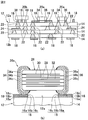
- FIG. 2A is a cross-sectional view taken along the line AA of the module shown in FIG.
- (b) is a principal part enlarged view which expands and shows the principal part of the module as described in (a).
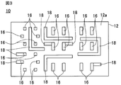
- 2 is a plan view showing a state of one main surface of a wiring board on which a land electrode part and a wiring conductor part are arranged in a module shown in FIG.
- FIG. 1 is a plan view of an embodiment of a module according to the present invention.
- 2A is a cross-sectional view of the module shown in FIG. 1
- FIG. 2B is an enlarged view of the main part showing the main part of the module shown in FIG. It is.
- FIG. 3 is a plan view showing a state of one main surface of the wiring board in which the land electrode portion and the wiring conductor portion are arranged in the module shown in FIG.
- the module 10 includes a wiring board 12.
- the wiring board 12 includes a large number of ceramic layers 14 as insulating layers, and is formed in multiple layers.
- a land electrode portion 16 and a wiring conductor portion 18 are disposed on one main surface 12 a of the wiring substrate 12.
- a wiring conductor portion 18 is disposed on the other main surface 12 b of the wiring board 12.
- the material of the ceramic layer 14 is preferably a low-temperature sintered ceramic material, for example.
- the low temperature sintered ceramic material is, for example, a material that can be sintered at a firing temperature of 1000 ° C. or less, and refers to a ceramic material that can be co-sintered with a low melting point metal such as Au, Ag, and Cu.
- Low-temperature sintered ceramic materials include, for example, glass composite materials obtained by mixing borosilicate glass with ceramic powder such as alumina and forsterite, and ZnO—MgO—Al 2 O 3 —SiO 2 crystallized glass. Crystallized glass materials used, non-glass materials using BaO—Al 2 O 3 —SiO 2 ceramic powder, Al 2 O 3 —CaO—SiO 2 —MgO—B 2 O 3 ceramic powder, etc. Can be mentioned.
- the land electrode portion 16 disposed on the one main surface 12a of the wiring board 12 is electrically connected to the surface mount components 20a and 20b mounted on the wiring board 12.
- the land electrode portion 16 includes a land electrode 16a, a Ni plating layer 16b, and a Sn plating layer 16c.
- Land electrode 16 a is formed on one main surface 12 a of wiring substrate 12.
- a conductive material having a small specific resistance can be used as the conductive material.
- a conductive material mainly composed of Cu or Ag that can be co-sintered with the low-temperature sintered ceramic material can be used.
- a Ni plating layer 16b containing Ni is formed on the surface of the land electrode 16a. Further, an Sn plating layer 16c is formed on the surface of the Ni plating layer 16b. That is, the Sn plating layer 16 c is formed on the outermost surface of the land electrode portion 16.
- the wiring conductor portion 18 disposed on the one main surface 12a and the other main surface 12b of the wiring substrate 12 is disposed so as to be electrically connected to the land electrode portion 16 or a via conductor 22 described later.
- the wiring conductor portion 18 disposed on the lower side of the surface mount component 20b may be disposed so as to contact the surface mount component 20b.
- the wiring conductor portion 18 includes a wiring conductor 18a, a Ni plating layer 18b, and a Sn plating layer 18c.
- a wiring conductor 18 a is formed on the one main surface 12 a and the other main surface 12 b of the wiring substrate 12.
- As the material of the wiring conductor 18a a conductive material having a small specific resistance can be used.
- a conductive material mainly composed of Cu or Ag that can be co-sintered with the low-temperature sintered ceramic material can be used.
- a Ni plating layer 18b containing Ni is formed on the surface of the wiring conductor 18a. Further, an Sn plating layer 18c is formed on the surface of the Ni plating layer 18b.
- a large number of via conductors 22 are provided so as to penetrate each ceramic layer 14 in the wiring board 12, and each via conductor 22 is electrically connected to the land electrode portion 16 and the wiring conductor portion 18. .
- An internal wiring conductor 24 is provided on the surface of each ceramic layer 14 located inside the wiring board 12, and each via conductor 22 is electrically connected to the internal wiring conductor 24 provided in each ceramic layer 14. It is connected to the.
- FIG. 2B shows a sectional ceramic capacitor as an example of a surface mount component 20a mounted on the wiring board 12 in a cross-sectional view.
- the multilayer ceramic capacitor shown in FIG. 2B includes a rectangular parallelepiped ceramic element 26.
- the ceramic element 26 includes a number of ceramic layers 28 made of, for example, a barium titanate dielectric ceramic as a dielectric. These ceramic layers 28 are laminated, and internal electrodes 30 and 32 made of, for example, Ni are alternately formed between the ceramic layers 28.
- the internal electrode 30 is formed with the other end extending to one end of the ceramic element 26, and the internal electrode 32 is formed with the other end extending to one end of the ceramic element 26.
- the internal electrodes 30 and 32 are formed so that the intermediate portion and the other end portion overlap with each other with the ceramic layer 28 interposed therebetween. Therefore, the ceramic element 26 has a laminated structure in which a plurality of internal electrodes 30 and 32 are provided via the ceramic layer 26.
- An external electrode portion 34 is provided on one end surface of the ceramic element 26.
- An external electrode portion 36 is provided on the other end surface of the ceramic element 26.
- the external electrode portion 34 includes an external electrode 34a, a Ni plating layer 34b, and a Sn plating layer 34c.
- the external electrode part 36 includes an external electrode 36a, a Ni plating layer 36b, and a Sn plating layer 36c.
- An external electrode 34 a made of, for example, Cu is formed on one end face of the ceramic element 26 so as to be electrically connected to the internal electrode 30.
- an external electrode 36 a made of, for example, Cu is formed on the other end surface of the ceramic element 26 so as to be electrically connected to the internal electrode 32.
- Ni plating layers 34b and 36b containing Ni are formed on the surfaces of the external electrodes 34a and 36a, respectively.
- Sn plating layers 34c and 36c are formed on the surfaces of the Ni plating layers 34b and 36b, respectively, to prevent oxidation. That is, the Sn plating layer 34 c is formed on the outermost surface of the external electrode portion 34, and the Sn plating layer 36 c is formed on the outermost surface of the external electrode portion 36.
- the external electrode portions 34 and 36 of the surface mount component 20a are electrically connected and mounted on the one main surface 12a of the wiring board 12 via the land electrode portion 16.
- the land electrode portion 16 and the external electrode portions 34 and 36 of the surface mount component 20a are connected via Sn. That is, as shown in FIG. 2B, in this module, the Sn plating layer 16c of the land electrode portion 16 disposed on the one main surface 12a of the wiring board 12 and the external electrode portions 34 and 36 of the surface mount component 20a are arranged. Only the portions necessary for the joining of the Sn plating layers 34c and 36c are joined via Sn. Each Sn plating layer 16c, 34c, 36c is preferably made of Sn alone.
- the land electrode portion 16 and the external electrode portions 34 and 36 of the surface mount component 20a only have to be connected via Sn, and between the land electrode 16a and the Sn plating layer 16c as in the present embodiment.
- Other members, such as Ni plating layers 16b, may be disposed, and other members, such as Ni plating layers 34b, 36b, are disposed between the external electrodes 34a, 36a and the Sn plating layers 34c, 36c. May be.
- the surface mount component 20b includes external terminal portions 38 and 40.
- An Sn plating layer (not shown) is formed on the outermost surfaces of the external terminal portions 38 and 40 in the same manner as the external electrode portions 34 and 36.
- the surface mount components 20a and 20b when the surface mount components 20a and 20b are mounted and joined to the wiring board 12, they are joined via Sn without using a bonding agent such as solder. Since Sn has a low melting point, it can be bonded at a low temperature. Further, when mounting the surface-mounted components 20a and 20b on the wiring board 12 and joining them, a short circuit occurs between the wiring conductors 18a due to the spread of solder or the spread of solder, which is a concern when joining using solder. There is no danger of this, and it is possible to join as much as desired.
- a bonding agent such as solder
- the wiring conductor portion is formed on the one main surface 12a of the wiring board 12. Since 18 can be arranged, the ceramic layer 14 can be reduced correspondingly. In addition, the wiring conductor portions 18 can be arranged close to each other on the one main surface 12a of the wiring substrate 12 and the density of the wiring conductor portions 18 can be improved. As a result, the size of the wiring substrate 12 can be reduced. A module that can be reduced in height and height can be obtained.
- the Sn in the land electrode portion 16 is Sn. Since the plating layer 16c is formed and the Sn plating layer 18c is formed in the wiring conductor portion 18, it is possible to avoid the occurrence of oxidation or the like in the land electrode portion 16 and the wiring conductor portion 18, and Can prevent scratches.
- the wiring conductor portion 18 disposed on the one main surface 12a of the wiring substrate 12 is disposed so as to contact the bottom surface of the surface mount component 20a,
- the wiring conductor portion 18 can be used as a heat dissipation circuit.
- this slurry is applied onto a carrier film by a doctor blade method or the like to produce a ceramic green sheet for low-temperature sintering. Thereafter, the ceramic green sheet is cut into a predetermined size. Through holes are formed in the obtained ceramic green sheet by laser processing, and a conductive paste for via filling is filled in the formed through holes.
- the conductive paste for land electrode to be the land electrode 16a and the conductive paste for wiring conductor to be the wiring conductor 18a are formed into a predetermined shape on the surface of the ceramic green sheet laminated on the upper layer by, for example, screen printing.
- the land electrode 16a and the wiring conductor 18a are formed by printing and drying.
- the conductive paste for internal wiring conductor is printed on the surface of the ceramic green sheet laminated on the second and subsequent layers in a predetermined shape by, for example, a screen printing method, and dried, so that the internal wiring conductor 24 is dried. Is formed.
- an unsintered ceramic laminated body is obtained by carrying out lamination
- the obtained unfired ceramic laminate is fired at a low temperature of, for example, 1050 ° C. or lower, whereby a sintered body can be obtained.
- the land electrode 16a and the wiring conductor 18a formed on the surface of the sintered body are subjected to Ni plating treatment and Sn plating treatment to obtain a desired wiring substrate 12, whereby the wiring substrate 12 is prepared.
- the surface-mounted component 20a to be prepared has external electrode portions 34 and 36, and the surface-mounted component 20b has external terminal portions 38 and 40.
- the external electrode portions 34 and 36 include external electrodes 34a and 36a, and Ni plating layers 34b and 36b and Sn plating layers 34c and 36c are formed in advance on the external electrodes 34a and 36a, respectively.
- an Sn plating layer is formed on the outermost surfaces of the external terminal portions 38 and 40.
- Reflow method is used as a method for mounting the prepared surface mount components 20a and 20b. That is, the surface mount components 20a and 20b are mounted such that the external electrode portions 34 and 36 of the surface mount component 20a or the external terminal portions 38 and 40 of the surface mount component 20b are in contact with the land electrode portion 16 on the wiring board 12. The reflow process is performed. Then, the Sn plating layers 34c and 36c of the external electrode portions 34 and 36 and the Sn plating layer 16c of the land electrode portion 16 in the surface mount component 20a are melted, so that the wiring board 12 and the surface mount component 20a are connected via Sn.
- the resist may or may not be disposed on one main surface of the wiring board.
- the thickness of the resist becomes unnecessary, the wiring board can be further reduced in height, and in addition, a module having a heat dissipation effect can be obtained.
- the present invention can be suitably used as a module used in an electronic device or the like that is required to be reduced in size and height.
Landscapes
- Engineering & Computer Science (AREA)
- Manufacturing & Machinery (AREA)
- Microelectronics & Electronic Packaging (AREA)
- Electric Connection Of Electric Components To Printed Circuits (AREA)
- Manufacturing Of Printed Wiring (AREA)
- Production Of Multi-Layered Print Wiring Board (AREA)
Abstract
配線基板を含むモジュールにおいて、その配線基板の表面に配置されたランド電極および配線導体が、はんだを介することなく表面実装部品と接合可能とすることで、小型化、低背化を可能にしたモジュールを提供する。 この発明にかかるモジュール10は、配線基板12を含む。配線基板12の一方主面12aには、ランド電極部16および配線導体部18が配置されている。ランド電極部16には、表面実装部品20a,20bが外部電極部34,36あるいは外部端子部38,40を介して接合される。表面実装部品20a,20bの外部電極部34,36あるいは外部端子部38,40は、ランド電極部16とSnを介して接合されて、表面実装部品20a,20bが実装される。
Description
この発明は、配線基板を含むモジュールおよびその製造方法に関し、特に、その配線基板の表面にランド電極および配線導体が配置されるモジュールおよびその製造方法に関する。
LTCC(低温同時焼成セラミックス:Low Temperature Co- fired Ceramics)による配線基板の表面に表面実装部品が実装される場合、通常、ランド電極を介して表面実装部品のみが実装され、LTCCによる配線基板の表面に配線導体が形成されることはない。
たとえば、特許文献1には、表面実装部品が、配線基板の表面に形成されたランド電極にはんだ実装され、そのランド電極に接続されるビア導体を介して配線基板の内部に形成されている配線導体に接続されたモジュールの構成が開示されている。特許文献1の記載において、表面実装部品は、はんだにより実装されるため、はんだの広がりによるショートを抑制するために、配線基板の表面にランド電極以外の配線導体は形成されず、多層基板の内部に形成される配線導体により配線が行われている。
上述した理由により、配線基板の表面にはランド電極しか配置されず、そのランド電極からビア導体で一層下に形成される配線導体に引き回されていることから、配線基板の表面には配線導体が形成されていない。そのため、表面実装部品の配線を配線基板の内部に引き込むと、そのビア導体の分だけ余計な絶縁層が必要になり、モジュールの小型化、低背化を困難にするという問題があった。加えて、このような配線基板では、配線基板の表面に配線導体の形成が困難であるため、配線基板の表層における高密度化への障害ともなっていた。
それゆえに、この発明の主たる目的は、配線基板を含むモジュールにおいて、その配線基板の表面に配置されたランド電極および配線導体が、はんだを介することなく表面実装部品と接合可能とすることで、小型化、低背化を可能にしたモジュールを提供することである。
この発明にかかるモジュールは、配線基板と、配線基板の一方主面に配置されるランド電極と、配線基板の一方主面に配置される配線導体と、ランド電極と接合するための外部電極を備える表面実装部品と、を含むモジュールであって、配線基板のランド電極および表面実装部品の外部電極の少なくとも一方の最表面にSn層を備え、表面実装部品の外部電極は、ランド電極とSnを介して接合されることを特徴とする、モジュールである。
また、本発明にかかるモジュールでは、配線基板のランド電極および表面実装部品の外部電極の最表面にSn層を備え、表面実装部品の外部電極は、ランド電極とSnを介して接合されることが好ましい。
また、この発明にかかるモジュールでは、配線導体が、ランド電極と接続されていることが好ましい。
さらに、この発明にかかるモジュールでは、配線導体は、表面実装部品の下部に配置されており、かつ、表面実装部品と接することが好ましい。
また、この発明にかかるモジュールでは、ランド電極および配線導体の表面には、Snめっき層が形成されていることが好ましい。
さらにまた、この発明にかかるモジュールでは、配線基板の一方主面には、レジストが配置されないことが好ましい。
この発明にかかるモジュールの製造方法は、配線基板を準備する工程であって、配線基板の一方主面には、ランド電極および配線導体が配置される、配線基板を準備する工程と、外部電極を備える表面実装部品を準備する工程と、を備えるモジュールの製造方法であって、配線基板のランド電極および表面実装部品の外部電極の少なくとも一方の最表面にSn層を備え、配線基板のランド電極と表面実装部品の外部電極とをSnを介して接合する工程を含む、モジュールの製造方法である。
また、配線基板のランド電極および表面実装部品の外部電極の最表面にSn層を備え、配線基板のランド電極と表面実装部品の外部電極とをSnを介して接合する工程を含むことが好ましい。
また、この発明にかかるモジュールの製造方法では、配線基板を準備する工程は、ランド電極および配線導体のそれぞれにSnめっき処理を施す工程を含むことが好ましい。
また、本発明にかかるモジュールでは、配線基板のランド電極および表面実装部品の外部電極の最表面にSn層を備え、表面実装部品の外部電極は、ランド電極とSnを介して接合されることが好ましい。
また、この発明にかかるモジュールでは、配線導体が、ランド電極と接続されていることが好ましい。
さらに、この発明にかかるモジュールでは、配線導体は、表面実装部品の下部に配置されており、かつ、表面実装部品と接することが好ましい。
また、この発明にかかるモジュールでは、ランド電極および配線導体の表面には、Snめっき層が形成されていることが好ましい。
さらにまた、この発明にかかるモジュールでは、配線基板の一方主面には、レジストが配置されないことが好ましい。
この発明にかかるモジュールの製造方法は、配線基板を準備する工程であって、配線基板の一方主面には、ランド電極および配線導体が配置される、配線基板を準備する工程と、外部電極を備える表面実装部品を準備する工程と、を備えるモジュールの製造方法であって、配線基板のランド電極および表面実装部品の外部電極の少なくとも一方の最表面にSn層を備え、配線基板のランド電極と表面実装部品の外部電極とをSnを介して接合する工程を含む、モジュールの製造方法である。
また、配線基板のランド電極および表面実装部品の外部電極の最表面にSn層を備え、配線基板のランド電極と表面実装部品の外部電極とをSnを介して接合する工程を含むことが好ましい。
また、この発明にかかるモジュールの製造方法では、配線基板を準備する工程は、ランド電極および配線導体のそれぞれにSnめっき処理を施す工程を含むことが好ましい。
この発明にかかるモジュールによれば、配線基板の一方主面に表面実装部品を実装して接合する際に、はんだなどの接合剤を用いることなくSnを介して接合されているので、Snの融点が低いことから、低温で接合させることができるモジュールを得ることができる。また、配線基板に表面実装部品を実装して接合する際に、Snを介して接合されているので、はんだを用いて接合する場合に懸念される、はんだの広がりやはんだが広がることによって配線基板の一方主面に配置される配線導体間においてショートが発生する危険がなく、所望の分だけ接合することができるモジュールが得られる。
また、この発明にかかるモジュールは、配線基板の一方主面に配置されるランド電極と配線導体とが接続されているので、配線基板の内部に形成されていた配線導体のパターンを配線基板の一方主面に形成できることから、配線基板を構成する層を減少させることができ、その結果、配線基板やモジュール全体として低背化することができる。
さらに、この発明にかかるモジュールでは、配線導体が、表面実装部品の下部に配置されており、かつ、表面実装部品と接するように配置されていることから、この配線導体を放熱回路として利用することができる。
また、この発明にかかるモジュールでは、ランド電極および配線導体の表面に、Snめっき層が形成されていることから、ランド電極や配線導体において酸化やキズが生じにくいモジュールを得ることができる。
さらに、この発明にかかるモジュールでは、配線基板の表面にレジストを配置しないことから、レジスト分の厚みが不要となり、その結果、配線基板を低背化できるとともに、放熱効果も有するモジュールを得ることができる。
この発明にかかるモジュールの製造方法では、配線基板に表面実装部品を実装して接合する際に、はんだなどの接合剤を用いることなく、融点の低いSnを介して接合するので、低温で接合させることができるモジュールを得ることができる。
また、この発明にかかるモジュールの製造方法では、配線基板を準備する工程において、ランド電極および配線導体のそれぞれにSnめっき処理を施すことから、ランド電極や配線導体に対して酸化等やキズが生じにくいモジュールを得ることができる。
また、この発明にかかるモジュールは、配線基板の一方主面に配置されるランド電極と配線導体とが接続されているので、配線基板の内部に形成されていた配線導体のパターンを配線基板の一方主面に形成できることから、配線基板を構成する層を減少させることができ、その結果、配線基板やモジュール全体として低背化することができる。
さらに、この発明にかかるモジュールでは、配線導体が、表面実装部品の下部に配置されており、かつ、表面実装部品と接するように配置されていることから、この配線導体を放熱回路として利用することができる。
また、この発明にかかるモジュールでは、ランド電極および配線導体の表面に、Snめっき層が形成されていることから、ランド電極や配線導体において酸化やキズが生じにくいモジュールを得ることができる。
さらに、この発明にかかるモジュールでは、配線基板の表面にレジストを配置しないことから、レジスト分の厚みが不要となり、その結果、配線基板を低背化できるとともに、放熱効果も有するモジュールを得ることができる。
この発明にかかるモジュールの製造方法では、配線基板に表面実装部品を実装して接合する際に、はんだなどの接合剤を用いることなく、融点の低いSnを介して接合するので、低温で接合させることができるモジュールを得ることができる。
また、この発明にかかるモジュールの製造方法では、配線基板を準備する工程において、ランド電極および配線導体のそれぞれにSnめっき処理を施すことから、ランド電極や配線導体に対して酸化等やキズが生じにくいモジュールを得ることができる。
この発明によれば、配線基板を含むモジュールにおいて、その配線基板の表面に配置されたランド電極および配線導体が、はんだを介することなく表面実装部品と接合可能とすることで、小型化、低背化を可能にしたモジュールが得られる。
この発明の上述の目的、その他の目的、特徴および利点は、図面を参照して行う以下の発明を実施するための形態の説明から一層明らかとなろう。
本発明にかかるモジュールの一実施の形態について説明する。図1は、本発明にかかるモジュールの一実施の形態の平面図である。また、図2(a)は、図1に記載のモジュールの断面図解図であり、図2(b)は、図2(a)に記載のモジュールの要部を拡大して示す要部拡大図である。また、図3は、図1に記載のモジュールにおいて、表面実装部品を取り除き、ランド電極部および配線導体部が配置された配線基板の一方主面の状態を示す平面図である。
この実施の形態にかかるモジュール10は、配線基板12を含む。配線基板12は、絶縁層として多数のセラミック層14を含み、多層に形成されている。配線基板12の一方主面12aには、ランド電極部16および配線導体部18が配置される。また、配線基板12の他方主面12bには、配線導体部18が配置される。
セラミック層14の材料は、たとえば、低温焼結セラミック材料を用いることが好ましい。低温焼結セラミック材料とは、たとえば、1000℃以下の焼成温度で焼結可能な材料であり、Au、Ag及びCu等の低融点金属と共焼結可能なセラミック材料のことをいう。低温焼結セラミック材料としては、たとえば、アルミナ、フォルステライト等のセラミック粉末にホウ珪酸系ガラスを混合してなるガラス複合系材料、ZnO-MgO-Al2O3-SiO2系の結晶化ガラスを用いた結晶化ガラス系材料、BaO-Al2O3-SiO2系セラミック粉末やAl2O3-CaO-SiO2-MgO-B2O3系セラミック粉末等を用いた非ガラス系材料等を挙げることができる。
また、図2(b)に示すように、配線基板12の一方主面12aに配置されるランド電極部16は、配線基板12に実装される表面実装部品20a,20bと電気的に接続するために設けられる。ランド電極部16は、ランド電極16a、Niめっき層16bおよびSnめっき層16cを含む。配線基板12の一方主面12aにランド電極16aが形成される。ランド電極16aの材料は、比抵抗の小さい導電性材料を用いることができる。導電性材料としては、たとえば、低温焼結セラミック材料と共焼結可能なCuやAgを主成分とする導電性材料を用いることができる。ランド電極16aの表面には、Niを含むNiめっき層16bが形成される。さらに、Niめっき層16bの表面には、Snめっき層16cが形成される。すなわち、ランド電極部16の最表面には、Snめっき層16cが形成される。
また、配線基板12の一方主面12aおよび他方主面12bに配置される配線導体部18は、ランド電極部16あるいは後述するビア導体22と電気的に接続されるように配置されている。なお、たとえば、図2(a)に示すように、表面実装部品20bの下部側に配置される配線導体部18は、表面実装部品20bに接するように配置してもよい。配線導体部18は、配線導体18a、Niめっき層18bおよびSnめっき層18cを含む。配線基板12の一方主面12aおよび他方主面12bに配線導体18aが形成される。配線導体18aの材料は、比抵抗の小さい導電性材料を用いることができる。導電性材料としては、たとえば、低温焼結セラミック材料と共焼結可能なCuやAgを主成分とする導電性材料を用いることができる。配線導体18aの表面には、Niを含むNiめっき層18bが形成される。さらに、Niめっき層18bの表面には、Snめっき層18cが形成される。
そして、配線基板12における各セラミック層14を貫通するように、多数のビア導体22が設けられており、各ビア導体22は、ランド電極部16および配線導体部18と電気的に接続されている。また、配線基板12の内部に位置する各セラミック層14の表面には、内部配線導体24が設けられており、各ビア導体22は、各セラミック層14に設けられた内部配線導体24と電気的に接続されている。
表面実装部品20a,20bとしては、たとえば、能動素子あるいは受動素子等が挙げられる。図2(b)には、配線基板12に実装される表面実装部品20aの一例として積層セラミックコンデンサを断面図解図で示している。図2(b)に示す積層セラミックコンデンサは、直方体状のセラミック素子26を含む。セラミック素子26は、誘電体としてたとえばチタン酸バリウム系の誘電体セラミックからなる多数のセラミック層28を含む。これらのセラミック層28は積層され、セラミック層28間には、たとえばNiからなる内部電極30および32が交互に形成される。この場合、内部電極30は他端部がセラミック素子26の一端部に延びて形成され、内部電極32は他端部がセラミック素子26の一端部に延びて形成される。また、内部電極30および32は、中間部および他端部がセラミック層28を介して重なり合うように形成される。したがって、このセラミック素子26は、内部にセラミック層26を介して複数の内部電極30および32が設けられた積層構造を有する。
セラミック素子26の一端面には、外部電極部34が設けられる。また、セラミック素子26の他端面には、外部電極部36が設けられる。外部電極部34は、外部電極34a、Niめっき層34bおよびSnめっき層34cを含む。また、外部電極部36は、外部電極36a、Niめっき層36bおよびSnめっき層36cを含む。
セラミック素子26の一端面には、たとえばCuからなる外部電極34aが内部電極30に電気的に接続されるように形成される。同様に、セラミック素子26の他端面には、たとえばCuからなる外部電極36aが内部電極32に電気的に接続されるように形成される。
また、外部電極34aおよび36aの表面には、Niを含むNiめっき層34bおよび36bがそれぞれ形成される。さらに、Niめっき層34bおよび36bの表面には、酸化防止のために、Snめっき層34cおよび36cがそれぞれ形成される。すなわち、外部電極部34の最表面にはSnめっき層34cが形成され、外部電極部36の最表面にはSnめっき層36cが形成される。
そして、配線基板12の一方主面12aには、ランド電極部16を介して表面実装部品20aの外部電極部34,36が電気的に接続されて実装される。ランド電極部16と表面実装部品20aの外部電極部34,36とは、Snを介して接続される。すなわち、図2(b)に示すように、このモジュールにおいて、配線基板12の一方主面12aに配置されるランド電極部16のSnめっき層16cと表面実装部品20aの外部電極部34,36のSnめっき層34c,36cとがSnを介して接合に必要な部分のみが接合される。各Snめっき層16c,34c,36cはSn単体からなるのが好ましい。なお、ランド電極部16と表面実装部品20aの外部電極部34,36がSnを介して接続されていればよく、本実施の形態のように、ランド電極16aとSnめっき層16cとの間に他の部材、たとえばNiめっき層16bが配置されていてもよいし、外部電極34a,36aと、Snめっき層34c,36cとの間に他の部材、たとえばNiめっき層34b,36bが配置されていてもよい。
また、表面実装部品20bは、外部端子部38,40を含む。外部端子部38,40の最表面には、外部電極部34,36と同様にSnめっき層(図示せず)が形成されている。そして、表面実装部品20bが配線基板12の一方主面12aに実装されると、表面実装部品20bの外部端子部38,40のSnめっき層とランド電極部16のSnめっき層16cとがSnを介して接合に必要な部分のみが接合される。
この実施の形態にかかるモジュール10によれば、配線基板12に表面実装部品20a,20bを実装して接合する際に、はんだなどの接合剤を用いることなく、Snを介して接合されているので、Snの融点の低いことから、低温で接合させることができる。また、配線基板12に表面実装部品20a,20bを実装して接合する際に、はんだを用いて接合する場合に懸念される、はんだの広がりやはんだが広がることによって配線導体18a間においてショートが発生する危険がなく、所望の分だけ接合することができる。
また、この実施の形態にかかるモジュール10によれば、配線基板12と表面実装部品20a,20bとの接合がはんだなどの接合剤を用いないので、配線基板12の一方主面12aに配線導体部18を配置させることができることから、その分、セラミック層14を減らすことができる。加えて、配線基板12の一方主面12a上に配線導体部18間を接近して配置させることができ、配線導体部18の密度を向上させることができることから、その結果、配線基板12の小型化、低背化を可能にしたモジュールを得ることができる。
また、この実施の形態にかかるモジュール10によれば、配線基板12の一方主面12aにランド電極部16および配線導体部18が形成されている場合であっても、ランド電極部16においてはSnめっき層16cが形成されており、配線導体部18においてはSnめっき層18cが形成されていることから、ランド電極部16および配線導体部18において酸化等が生ずることを回避することができるとともに、キズがつくことを防ぐことができる。
また、この実施の形態にかかるモジュール10によれば、配線基板12の一方主面12aに配置される配線導体部18が、表面実装部品20aの底面と接するように配置されている場合には、配線導体部18を放熱回路として利用することができる。
次に、本発明にかかるモジュールの製造方法の一実施の形態について説明する。
まず、低温焼結セラミック材料をビニルアルコール系バインダ中に分散させてスラリーを調製した後、このスラリーをドクターブレード法等によってキャリアフィルム上に塗布して低温焼結用のセラミックグリーンシートを作製する。その後、セラミックグリーンシートを所定の大きさに切断する。得られたセラミックグリーンシートに対して、レーザ加工することによって貫通孔を形成し、形成された貫通孔内にビア充填用導電性ペーストを充填する。
次いで、ランド電極16aとなるランド電極用導電性ペーストおよび配線導体18aとなる配線導体用導電性ペーストが、たとえば、スクリーン印刷法にて、上層に積層されるセラミックグリーンシートの表面に所定の形状にて印刷し、乾燥することにより、ランド電極16aおよび配線導体18aが形成される。また、2層目以降に積層されるセラミックグリーンシートの表面には、内部配線導体用導電性ペーストが、たとえば、スクリーン印刷法にて所定の形状に印刷し、乾燥することにより、内部配線導体24が形成される。そして、ランド電極16aおよび配線導体18aが形成されたセラミックグリーンシートが上層となるように、所定の様式、方法にて、積層、圧着することにより、未焼成のセラミック積層体が得られる。
その後、得られた未焼成のセラミック積層体を、たとえば1050℃以下の低温で焼成することにより、焼結体を得ることができる。そして、この焼結体の表面に形成されるランド電極16aおよび配線導体18aに対して、Niめっき処理およびSnめっき処理が施され、所望の配線基板12を得ることで、配線基板12が準備される。
続いて、準備された配線基板12に実装される表面実装部品20a,20bが準備される。準備される表面実装部品20aは、外部電極部34,36を有し、表面実装部品20bは、外部端子部38,40を有する。外部電極部34,36は、外部電極34a,36aを含み、外部電極34a,36aには、それぞれ予めNiめっき層34b,36bおよびSnめっき層34c,36cが形成されている。同様に、外部端子部38,40の最表面には、Snめっき層が形成されている。
準備された表面実装部品20a,20bの実装方法としては、リフロー工法が用いられる。すなわち、表面実装部品20a,20bは、その表面実装部品20aの外部電極部34,36あるいは表面実装部品20bの外部端子部38,40が、配線基板12におけるランド電極部16に接するように実装され、リフロー処理される。そうすると、表面実装部品20aにおける外部電極部34,36のSnめっき層34c,36cとランド電極部16のSnめっき層16cとがそれぞれ溶融することで、Snを介して配線基板12と表面実装部品20aとが接合され、同様に、表面実装部品20bにおける外部端子部38,40のSnめっき層とランド電極部16のSnめっき層16cとがそれぞれ溶融することで、Snを介して配線基板12と表面実装部品20bとが接合される。そして、所望のモジュール10を得ることができる。
この実施の形態にかかるモジュールの製造方法によれば、リフロー工法によって配線基板12と表面実装部品20a,20bとが、融点が232℃と低いSnを介して接合しているので、はんだを介することなく低温で接合させることができる。
また、この実施の形態にかかるモジュールの製造方法によれば、配線基板12と表面実装部品20a,20bとの接合に際して、Snを介して接合されるので、表面実装部品20a,20bを配線基板12の一方主面12aに実装する場合、はんだなどの接合剤を用いることがないことから、はんだの広がりやはんだが広がることによって、配線基板12の一方主面に配置される配線導体間においてショートが発生する危険がなく、所望の分だけ接合させることができる。
さらに、この実施の形態にかかるモジュールの製造方法によれば、ランド電極16aおよび配線導体18aに対してSnめっき処理が施される工程を含んでおり、ランド電極16aにSnめっき層16cが形成され、配線導体18aにSnめっき層18cが形成されることから、ランド電極部16や配線導体部18に対して酸化やキズが生じにくいモジュールを得ることができる。
なお、この発明は、上述した実施の形態に限定されるものではなく、その要旨の範囲内で種々に変形される。
たとえば、本実施の形態にかかるモジュールでは、配線基板の一方主面において、レジストが配置されていても、配置されていなくてもよい。配線基板の一方主面にレジストが配置されていない場合は、レジスト分の厚みが不要となり、配線基板をさらに低背化することができ、加えて、放熱効果も有したモジュールを得ることができる。
また、本実施の形態にかかるモジュールでは、配線基板の一方主面に配置されるランド電極の最表面にSnめっき層が形成され、表面実装部品の外部電極部等の最表面にSnめっき層が形成され、それぞれのSnめっき層が接合されることによって、配線基板の一方主面に表面実装部品がSnを介して実装されているが、これに限るものではなく、ランド電極部および表面実装部品の外部電極部等のうち少なくともいずれか一方の最表面にSnめっき層が形成されることで、配線基板の一方主面に表面実装部品がSnを介して実装されてもよい。
また、Snめっき層としてSn層は、湿式めっきや蒸着やスパッタなどの乾式めっき等のめっき法により形成されるものに限られず、Snペーストを塗布したり、印刷法、インクジェット法によって形成してもよい。
また、Snめっき層としてSn層は、湿式めっきや蒸着やスパッタなどの乾式めっき等のめっき法により形成されるものに限られず、Snペーストを塗布したり、印刷法、インクジェット法によって形成してもよい。
また、本実施の形態にかかるモジュールでは、配線基板は多層に形成されているが、これに限るものではなく、単層の配線基板でもよい。
本発明は、小型化、低背化が求められる電子機器等に用いられるモジュールとして好適に利用することができる。
10 モジュール
12 配線基板
12a 一方主面
12b 他方主面
14 セラミック層
16 ランド電極部
16a ランド電極
16b Niめっき層
16c Snめっき層
18 配線導体部
18a 配線導体
18b Niめっき層
18c Snめっき層
20a、20b 表面実装部品
22 ビア導体
24 内部配線導体
26 セラミック素子
28 セラミック層
30、32 内部電極
34、36 外部電極部
34a、36a 外部電極
34b、36b Niめっき層
34c、34c Snめっき層
38、40 外部端子部
12 配線基板
12a 一方主面
12b 他方主面
14 セラミック層
16 ランド電極部
16a ランド電極
16b Niめっき層
16c Snめっき層
18 配線導体部
18a 配線導体
18b Niめっき層
18c Snめっき層
20a、20b 表面実装部品
22 ビア導体
24 内部配線導体
26 セラミック素子
28 セラミック層
30、32 内部電極
34、36 外部電極部
34a、36a 外部電極
34b、36b Niめっき層
34c、34c Snめっき層
38、40 外部端子部
Claims (9)
- 配線基板と、
前記配線基板の一方主面に配置されるランド電極と、
前記配線基板の一方主面に配置される配線導体と、
前記ランド電極と接合するための外部電極を備える表面実装部品と、
を含むモジュールであって、
前記配線基板の前記ランド電極および前記表面実装部品の前記外部電極の少なくとも一方の最表面にSn層を備え、
前記表面実装部品の前記外部電極は、前記ランド電極と前記Snを介して接合されることを特徴とする、モジュール。 - 前記配線基板の前記ランド電極および前記表面実装部品の前記外部電極の最表面にSn層を備え、
前記表面実装部品の前記外部電極は、前記ランド電極と前記Snを介して接合されることを特徴とする、請求項1に記載のモジュール。 - 前記配線導体は、前記ランド電極と接続されていることを特徴とする、請求項1または請求項2に記載のモジュール。
- 前記配線導体は、前記表面実装部品の下部に配置されており、かつ、前記表面実装部品と接することを特徴とする、請求項1ないし請求項3のいずれかに記載のモジュール。
- 前記ランド電極および前記配線導体の表面には、Snめっき層が形成されていることを特徴とする、請求項1ないし請求項4のいずれかに記載のモジュール。
- 前記配線基板の一方主面には、レジストが配置されないことを特徴とする、請求項1ないし請求項5のいずれかに記載のモジュール。
- 配線基板を準備する工程であって、前記配線基板の一方主面には、ランド電極および配線導体が配置される、前記配線基板を準備する工程と、
外部電極を備える表面実装部品を準備する工程と、
を備えるモジュールの製造方法であって、
前記配線基板の前記ランド電極および前記表面実装部品の前記外部電極の少なくとも一方の最表面にSn層を備え、
前記配線基板の前記ランド電極と前記表面実装部品の前記外部電極とを前記Snを介して接合する工程を含む、モジュールの製造方法。 - 前記配線基板の前記ランド電極および前記表面実装部品の前記外部電極の最表面にSn層を備え、
前記配線基板の前記ランド電極と前記表面実装部品の前記外部電極とを前記Snを介して接合する工程を含む、請求項7に記載のモジュールの製造方法。 - 前記配線基板を準備する工程は、
前記ランド電極および前記配線導体のそれぞれにSnめっき処理を施す工程を含む、請求項7または請求項8に記載のモジュールの製造方法。
Priority Applications (1)
| Application Number | Priority Date | Filing Date | Title |
|---|---|---|---|
| JP2014558424A JP6164228B2 (ja) | 2013-01-25 | 2013-08-12 | モジュールおよびその製造方法 |
Applications Claiming Priority (2)
| Application Number | Priority Date | Filing Date | Title |
|---|---|---|---|
| JP2013012541 | 2013-01-25 | ||
| JP2013-012541 | 2013-01-25 |
Publications (1)
| Publication Number | Publication Date |
|---|---|
| WO2014115358A1 true WO2014115358A1 (ja) | 2014-07-31 |
Family
ID=51227167
Family Applications (1)
| Application Number | Title | Priority Date | Filing Date |
|---|---|---|---|
| PCT/JP2013/071821 Ceased WO2014115358A1 (ja) | 2013-01-25 | 2013-08-12 | モジュールおよびその製造方法 |
Country Status (2)
| Country | Link |
|---|---|
| JP (1) | JP6164228B2 (ja) |
| WO (1) | WO2014115358A1 (ja) |
Cited By (1)
| Publication number | Priority date | Publication date | Assignee | Title |
|---|---|---|---|---|
| KR20160148479A (ko) * | 2015-06-16 | 2016-12-26 | 가부시키가이샤 무라타 세이사쿠쇼 | 복합 전자 부품 |
Citations (3)
| Publication number | Priority date | Publication date | Assignee | Title |
|---|---|---|---|---|
| JP2009158868A (ja) * | 2007-12-27 | 2009-07-16 | Seiko Epson Corp | 電子回路装置および電子機器 |
| JP2010258019A (ja) * | 2009-04-21 | 2010-11-11 | Murata Mfg Co Ltd | 樹脂多層モジュール及び樹脂多層モジュールの製造方法 |
| JP2011200930A (ja) * | 2010-03-26 | 2011-10-13 | Gunma Univ | 金属部材の接合方法 |
Family Cites Families (9)
| Publication number | Priority date | Publication date | Assignee | Title |
|---|---|---|---|---|
| JPH02217182A (ja) * | 1989-02-16 | 1990-08-29 | Kobe Steel Ltd | 銅又は銅合金材の接合方法 |
| JPH0422115A (ja) * | 1990-05-17 | 1992-01-27 | Murata Mfg Co Ltd | セラミック電子部品及びその製造方法 |
| JPH06103810A (ja) * | 1992-08-06 | 1994-04-15 | Murata Mfg Co Ltd | 導電ペースト |
| JP3019703B2 (ja) * | 1993-12-27 | 2000-03-13 | 株式会社村田製作所 | セラミック電子部品の製造方法 |
| JP3677983B2 (ja) * | 1998-02-05 | 2005-08-03 | 株式会社村田製作所 | セラミック基板 |
| JP4984171B2 (ja) * | 2008-04-01 | 2012-07-25 | 日本電信電話株式会社 | 光半導体素子の実装構造および光半導体素子の実装方法 |
| JP4984170B2 (ja) * | 2008-04-01 | 2012-07-25 | 日本電信電話株式会社 | 光半導体素子の実装構造 |
| JP5644286B2 (ja) * | 2010-09-07 | 2014-12-24 | オムロン株式会社 | 電子部品の表面実装方法及び電子部品が実装された基板 |
| KR20140110926A (ko) * | 2012-03-05 | 2014-09-17 | 가부시키가이샤 무라타 세이사쿠쇼 | 접합 방법, 접합 구조체 및 그 제조 방법 |
-
2013
- 2013-08-12 WO PCT/JP2013/071821 patent/WO2014115358A1/ja not_active Ceased
- 2013-08-12 JP JP2014558424A patent/JP6164228B2/ja active Active
Patent Citations (3)
| Publication number | Priority date | Publication date | Assignee | Title |
|---|---|---|---|---|
| JP2009158868A (ja) * | 2007-12-27 | 2009-07-16 | Seiko Epson Corp | 電子回路装置および電子機器 |
| JP2010258019A (ja) * | 2009-04-21 | 2010-11-11 | Murata Mfg Co Ltd | 樹脂多層モジュール及び樹脂多層モジュールの製造方法 |
| JP2011200930A (ja) * | 2010-03-26 | 2011-10-13 | Gunma Univ | 金属部材の接合方法 |
Cited By (4)
| Publication number | Priority date | Publication date | Assignee | Title |
|---|---|---|---|---|
| KR20160148479A (ko) * | 2015-06-16 | 2016-12-26 | 가부시키가이샤 무라타 세이사쿠쇼 | 복합 전자 부품 |
| CN106257610A (zh) * | 2015-06-16 | 2016-12-28 | 株式会社村田制作所 | 复合电子部件 |
| KR101900375B1 (ko) * | 2015-06-16 | 2018-09-19 | 가부시키가이샤 무라타 세이사쿠쇼 | 복합 전자 부품 |
| US10121593B2 (en) | 2015-06-16 | 2018-11-06 | Murata Manufacturing Co., Ltd. | Composite electronic component |
Also Published As
| Publication number | Publication date |
|---|---|
| JP6164228B2 (ja) | 2017-07-19 |
| JPWO2014115358A1 (ja) | 2017-01-26 |
Similar Documents
| Publication | Publication Date | Title |
|---|---|---|
| KR102112107B1 (ko) | 전자부품 및 전자부품의 제조 방법 | |
| KR101659153B1 (ko) | 적층 세라믹 커패시터, 적층 세라믹 커패시터의 제조방법 및 적층 세라믹 커패시터의 실장 기판 | |
| JP6376604B2 (ja) | 基板内蔵用積層セラミック電子部品及び積層セラミック電子部品内蔵型印刷回路基板 | |
| JP3535998B2 (ja) | 積層セラミック電子部品 | |
| JP2021015950A (ja) | 積層セラミックコンデンサ | |
| KR20140014773A (ko) | 적층 세라믹 전자부품 및 이의 제조방법 | |
| JP2019004080A (ja) | 電子部品、電子装置、及び電子部品の製造方法 | |
| KR20140081360A (ko) | 적층 세라믹 커패시터, 그 제조방법 및 적층 세라믹 커패시터가 실장된 회로기판 | |
| US7417196B2 (en) | Multilayer board with built-in chip-type electronic component and manufacturing method thereof | |
| JP4310468B2 (ja) | セラミック多層基板及びその製造方法 | |
| JP2014216643A (ja) | 積層セラミック電子部品及びその実装基板 | |
| JP6503943B2 (ja) | 複合電子部品および抵抗素子 | |
| JP4463045B2 (ja) | セラミック電子部品及びコンデンサ | |
| JP6962178B2 (ja) | 電子部品 | |
| JP2003022929A (ja) | 積層セラミックコンデンサ | |
| JP6164228B2 (ja) | モジュールおよびその製造方法 | |
| JP4329762B2 (ja) | チップ型電子部品内蔵型多層基板 | |
| KR102078015B1 (ko) | 커패시터 내장형 저온동시소성 세라믹 기판 | |
| JP7055588B2 (ja) | 電子部品 | |
| JP4752612B2 (ja) | 突起電極付き回路基板の製造方法 | |
| JP2012146940A (ja) | 電子部品および電子装置 | |
| JP2005294618A (ja) | 電子部品 | |
| JP4463046B2 (ja) | セラミック電子部品及びコンデンサ | |
| JP5838978B2 (ja) | セラミック積層部品 | |
| JP2006041319A (ja) | 表面実装型多連コンデンサ及びその実装構造 |
Legal Events
| Date | Code | Title | Description |
|---|---|---|---|
| 121 | Ep: the epo has been informed by wipo that ep was designated in this application |
Ref document number: 13873120 Country of ref document: EP Kind code of ref document: A1 |
|
| ENP | Entry into the national phase |
Ref document number: 2014558424 Country of ref document: JP Kind code of ref document: A |
|
| NENP | Non-entry into the national phase |
Ref country code: DE |
|
| 122 | Ep: pct application non-entry in european phase |
Ref document number: 13873120 Country of ref document: EP Kind code of ref document: A1 |