WO2014069250A1 - 光学部品、光学部品の製造方法、及びゴースト光の定量方法 - Google Patents
光学部品、光学部品の製造方法、及びゴースト光の定量方法 Download PDFInfo
- Publication number
- WO2014069250A1 WO2014069250A1 PCT/JP2013/078280 JP2013078280W WO2014069250A1 WO 2014069250 A1 WO2014069250 A1 WO 2014069250A1 JP 2013078280 W JP2013078280 W JP 2013078280W WO 2014069250 A1 WO2014069250 A1 WO 2014069250A1
- Authority
- WO
- WIPO (PCT)
- Prior art keywords
- multilayer film
- refractive index
- wavelength
- plastic substrate
- optical component
- Prior art date
- Legal status (The legal status is an assumption and is not a legal conclusion. Google has not performed a legal analysis and makes no representation as to the accuracy of the status listed.)
- Ceased
Links
Images





Classifications
-
- G—PHYSICS
- G02—OPTICS
- G02C—SPECTACLES; SUNGLASSES OR GOGGLES INSOFAR AS THEY HAVE THE SAME FEATURES AS SPECTACLES; CONTACT LENSES
- G02C7/00—Optical parts
- G02C7/10—Filters, e.g. for facilitating adaptation of the eyes to the dark; Sunglasses
- G02C7/107—Interference colour filters
-
- G—PHYSICS
- G02—OPTICS
- G02C—SPECTACLES; SUNGLASSES OR GOGGLES INSOFAR AS THEY HAVE THE SAME FEATURES AS SPECTACLES; CONTACT LENSES
- G02C7/00—Optical parts
- G02C7/02—Lenses; Lens systems ; Methods of designing lenses
-
- G—PHYSICS
- G02—OPTICS
- G02B—OPTICAL ELEMENTS, SYSTEMS OR APPARATUS
- G02B1/00—Optical elements characterised by the material of which they are made; Optical coatings for optical elements
- G02B1/04—Optical elements characterised by the material of which they are made; Optical coatings for optical elements made of organic materials, e.g. plastics
- G02B1/041—Lenses
-
- G—PHYSICS
- G02—OPTICS
- G02B—OPTICAL ELEMENTS, SYSTEMS OR APPARATUS
- G02B1/00—Optical elements characterised by the material of which they are made; Optical coatings for optical elements
- G02B1/10—Optical coatings produced by application to, or surface treatment of, optical elements
- G02B1/11—Anti-reflection coatings
-
- G—PHYSICS
- G02—OPTICS
- G02B—OPTICAL ELEMENTS, SYSTEMS OR APPARATUS
- G02B1/00—Optical elements characterised by the material of which they are made; Optical coatings for optical elements
- G02B1/10—Optical coatings produced by application to, or surface treatment of, optical elements
- G02B1/18—Coatings for keeping optical surfaces clean, e.g. hydrophobic or photo-catalytic films
-
- G—PHYSICS
- G02—OPTICS
- G02B—OPTICAL ELEMENTS, SYSTEMS OR APPARATUS
- G02B27/00—Optical systems or apparatus not provided for by any of the groups G02B1/00 - G02B26/00, G02B30/00
- G02B27/0012—Optical design, e.g. procedures, algorithms, optimisation routines
-
- G—PHYSICS
- G02—OPTICS
- G02B—OPTICAL ELEMENTS, SYSTEMS OR APPARATUS
- G02B27/00—Optical systems or apparatus not provided for by any of the groups G02B1/00 - G02B26/00, G02B30/00
- G02B27/0018—Optical systems or apparatus not provided for by any of the groups G02B1/00 - G02B26/00, G02B30/00 with means for preventing ghost images
-
- G—PHYSICS
- G02—OPTICS
- G02C—SPECTACLES; SUNGLASSES OR GOGGLES INSOFAR AS THEY HAVE THE SAME FEATURES AS SPECTACLES; CONTACT LENSES
- G02C2202/00—Generic optical aspects applicable to one or more of the subgroups of G02C7/00
- G02C2202/16—Laminated or compound lenses
Definitions
- the present invention relates to an optical component, an optical component manufacturing method, and a ghost light quantification method.
- plastic lenses are frequently used as spectacle lenses because of their advantages of being lightweight, excellent in impact resistance and easy to dye.
- a plastic lens used for a spectacle lens is usually provided with an antireflection film on both sides.
- the antireflection film for spectacle lenses generally has low reflection characteristics (broadband low reflection characteristics) over the entire visible region of 400 nm to 700 nm.
- optical parts such as eyeglass lenses
- optical parts including a plastic base as disclosed in Patent Documents 1 to 3, and an antireflection film disposed on the base.
- dyeing lenses such as sunglasses are known.
- the dyed lens cuts the entire visible region, the visibility may deteriorate due to a decrease in the amount of light.
- this method has a high reflectivity of the multilayer film, and causes strong multiple reflection within the lens, which may cause clear ghost light to enter the field of view.
- An aspect of the present invention has an antiglare effect, reduces fatigue, is effective in preventing eye diseases, and has a relatively high reflectivity and good visibility, and manufacture of an optical component It aims to provide a method. Another object of the present invention is to provide a method for quantifying ghost light generated by multiple reflection of light within an optical component.
- An optical component according to an aspect of the present invention is an optical component comprising a plastic substrate and a multilayer film disposed on both surfaces of the plastic substrate, the plastic substrate including the plastic substrate.
- the spectral characteristic curve showing the relationship between the wavelength and the reflectance with respect to the multilayer film disposed on the one surface has a maximum value at the first wavelength in the wavelength range of 380 to 780 nm, and the first wavelength
- the average reflectance of the multilayer film disposed on the one surface is 50% or less in a wavelength range of 25 nm before and after the first wavelength from the first wavelength to the second wavelength within 200 nm from the long wavelength side.
- the average reflectance of the multilayer film disposed on the two surfaces of the plastic substrate in the wavelength range of about 25 nm before and after the first wavelength is that of the multilayer film disposed on the one surface.
- Average reflectance The spectral characteristic curve showing the relationship between the wavelength and the reflectance with respect to the multilayer film disposed on the two surfaces of the plastic base material is 0% or less, in the wavelength range of 25 nm before and after the first wavelength, It does not have a maximum value.
- An optical component manufacturing method is a method for manufacturing an optical component comprising a plastic substrate and a multilayer film disposed on both surfaces of the plastic substrate. And heating the plastic substrate, and adjusting the plastic substrate to a predetermined temperature by the heating, and then forming the multilayer film on the plastic substrate.
- the forming step includes a step of alternately stacking a plurality of high refractive index materials and low refractive index materials to form a high refractive index layer having a multilayer structure, and a low refractive index having a refractive index lower than the refractive index of the high refractive index layer.
- Spectral characteristic curve is 380-780n In the wavelength range of 25 nm before and after the first wavelength, the first wavelength has one local maximum value at the first wavelength and the second wavelength within 200 nm from the first wavelength to the long wavelength side.
- the multilayer film disposed on the one surface has an average reflectance of 50% or less, and is disposed on the two surfaces of the plastic substrate in the wavelength range of 25 nm before and after the first wavelength.
- the spectral characteristic curve showing the relationship between the wavelength and the reflectance with respect to the reference wavelength is set so as not to have a maximum value in the wavelength range of 25 nm before and after the first wavelength.
- a ghost light quantification method is an optical component comprising a plastic substrate and a multilayer film disposed on both surfaces of the plastic substrate. Quantification method of ghost light generated by multiple reflections of the multi-layer, wherein the spectral reflectance R 1 ( ⁇ ) [%] of the multilayer film disposed on the one surface and the spectrum of the multilayer film disposed on the two surfaces From the reflectance R 2 ( ⁇ ) [%] and the following equation (1), A n ( ⁇ ) is obtained.
- n an integer of 1 or more.
- n an integer of 1 or more.
- the value of the Y value is the intensity of ghost light.
- optical component according to the aspect of the present invention even when a multilayer film having a high reflectance is provided, a sufficient antiglare effect can be obtained while maintaining good visibility.
- the method of manufacturing an optical component according to an aspect of the present invention it is possible to provide an optical component that has optical characteristics that reduce multiple reflections in the lens, are easy to see, and are effective in preventing fatigue and eye diseases. It becomes possible.
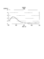
- FIG. 6 is a spectral characteristic diagram on one surface of the lens of Example 1.
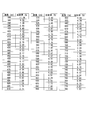
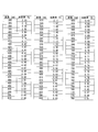
- FIG. 5A is numerical data of the spectral characteristics of FIG. 5A.
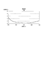
- 2 is a spectral characteristic diagram on two surfaces of the lens of Example 1.
- FIG. 6A is numerical data of the spectral characteristics of FIG. 6A.
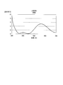
- FIG. 6 is a spectral characteristic diagram on one surface of a lens according to Example 2.
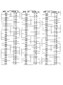
- FIG. It is numerical data of the spectral characteristics of FIG. 7A. 6 is a spectral characteristic diagram on two surfaces of the lens of Example 2.
- FIG. It is numerical data of the spectral characteristic of FIG. 8A. 6 is a spectral characteristic diagram on one surface of a lens according to Example 3.
- FIG. It is numerical data of the spectral characteristics of FIG. 9A. 6 is a spectral characteristic diagram on two surfaces of the lens of Example 3.
- FIG. It is numerical data of the spectral characteristics of FIG. 10A. 6 is a spectral characteristic diagram on both surfaces of the lens of Comparative Example 1.
- FIG. It is numerical data of the spectral characteristic of FIG. 11A. 6 is a spectral characteristic diagram on both surfaces of a lens of Comparative Example 2.
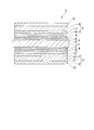
- FIG. 1 is a side sectional view schematically showing an optical component according to an embodiment of the present invention.
- reference numeral 1 denotes an optical component for a spectacle lens.
- the optical component 1 includes a plastic substrate 2 and an inorganic multilayer film 3 disposed on one surface of the plastic substrate 2.
- a functional thin film 4 is disposed between one surface of the plastic substrate 2 and the inorganic multilayer film 3.
- the functional thin film 4 is composed of a primer layer 5 and a hard coat layer 6 in this embodiment.
- the plastic substrate 2 is, for example, a transparent plastic such as acrylic resin, thiourethane resin, methacrylic resin, allyl resin, episulfide resin, polycarbonate resin, polyurethane resin, polyester resin, polystyrene resin, episulfide.
- the refractive index (nd) of the plastic substrate 2 is selected from, for example, 1.50, 1.60, 1.67, and 1.74.
- the plastic base material 2 when making the refractive index of the plastic base material 2 1.6 or more, an allyl carbonate resin, an acrylate resin, a methacrylate resin, a thiourethane resin, or the like can be used. .
- the plastic substrate 2 may not be transparent as long as it has translucency, and may be colored. The transmittance of the colored plastic substrate 2 can be 5 to 85%.
- the functional thin film 4 is disposed between the plastic substrate 2 and the inorganic multilayer film 3 as described above, and is in contact with the primer layer 5 disposed in contact with the plastic substrate 2, and
- the hard coat layer 6 is disposed in contact with the inorganic multilayer film 3.
- the primer layer 5 is for improving the adhesion between the plastic substrate 2 and the hard coat layer 6 and functions as an adhesion layer. Moreover, it is also for absorbing the impact on the optical component 1 and functions as an impact absorbing layer.
- the primer layer 5 is mainly composed of a polyurethane-based resin, and in this embodiment, the polyurethane-based resin contains, for example, fine particles of an inorganic material.
- the primer layer 5 may include at least one of acrylic resin, methacrylic resin, and organosilicon resin.
- the thickness (actual thickness) of the primer layer 5 can be about 0.5 ⁇ m or more and 1.0 ⁇ m or less.
- the primer layer 5 can be formed on the plastic substrate 2 with a predetermined thickness by immersing the plastic substrate 2 in the forming material solution of the primer layer 5 and then lifting and drying.
- a material for forming the primer layer 5 for example, a solution obtained by dispersing or dissolving the resin to be the primer layer 5 and the inorganic oxide fine particle sol in water or an alcohol solvent and mixing them can be used.
- the hard coat layer 6 has a function of protecting the plastic substrate 2 and suppressing damage to the plastic substrate 2, and functions as a scratch-resistant film.
- the hard coat layer 6 is made of, for example, an organosiloxane hard coat layer.
- the organosiloxane hard coat layer is obtained by dispersing inorganic oxide fine particles in an organosiloxane resin.
- the inorganic oxide for example, rutile-type titanium oxide, and oxides of silicon, tin, zirconium, and antimony are used.
- the hard coat layer 6 may be an organic silicon-based resin containing colloidal silica as disclosed in, for example, Japanese Patent Publication No. 4-55615.
- the thickness (actual thickness) of the hard coat layer 6 can be about 2 ⁇ m or more and 4 ⁇ m or less.
- the hard coat layer 6 is formed on the primer layer 5 on the plastic substrate 2 by immersing the plastic substrate 2 on which the primer layer 5 is formed in the forming material solution of the hard coat layer 6, and then pulling up and drying. It can be formed with a thickness of As a forming material liquid for the hard coat layer 6, for example, a liquid obtained by dispersing or dissolving the resin to be the hard coat layer 6 and the inorganic oxide fine particle sol in water or an alcohol solvent and mixing them can be used. .
- the functional thin film 4 and the plastic substrate 2 can be used as long as the refractive index and the refractive index of the plastic substrate 2 are substantially the same. Generation of interference fringes caused by reflection at the interface and a decrease in transmittance can be suppressed. Therefore, the refractive index of the functional thin film 4 is adjusted according to the refractive index of the plastic substrate 2.
- the refractive index of the functional thin film 4 (primer layer 5 and hard coat layer 6) can be adjusted by selecting the type (physical properties) of the resin that is the main component of the functional thin film 4, or for the resin that is the main component. This can be done by selecting the type (physical properties) of the fine particles to be added.
- the functional thin film 4 is formed including the primer layer 5 and the hard coat layer 6.
- the primer layer 5 and the hard coat layer 6 are formed. It may be omitted.
- a dielectric film or a metal film made of ITO (Indium Tin Oxide) or the like may be provided in addition to the primer layer 5 and the hard coat layer 6.
- a dielectric film or a metal film having a thickness of 20 nm or less may be disposed between the high refractive index inorganic material and the low refractive index inorganic material constituting the inorganic multilayer film. Note that the thickness of the dielectric film or the metal film may be 10 nm or less.
- the inorganic multilayer film 3 includes a high refractive index layer 7 having a multilayer structure in which a plurality of high refractive index inorganic materials and low refractive index inorganic materials are alternately stacked on the plastic substrate 2.
- the low refractive index layer 8 made of a low refractive index inorganic material having a lower refractive index than that of the high refractive index layer 7 is formed into a multilayer.
- the inorganic multilayer film 3 has a function as an antireflection film for preventing reflection of incident light.
- an inorganic multilayer film is used as the multilayer film.
- an organic multilayer film may be used as long as the effects of the present invention are not impaired.
- the high refractive index layer 7 is made of the first layer 9 made of a high refractive index inorganic material provided on the plastic substrate 2 side, and the low refractive index inorganic material provided on the first layer 9. It consists of a second layer 10 and a third layer 11 made of a high refractive index inorganic material provided on the second layer 10.
- the first layer 9 is provided in contact with the hard coat layer 6 and is made of zirconium dioxide (ZrO 2 ) having a refractive index of 2.0.
- ZrO 2 zirconium dioxide
- titanium dioxide (TiO 2 ) or tantalum dioxide (Ta 2 O 5 ) can be used as the high refractive index inorganic material constituting the first layer 9.
- it can also be formed of an oxide of an alloy composed of a plurality of kinds of zirconium, titanium, and tantalum.
- Y 2 O 3 yttrium dioxide
- Nb 2 O 5 niobium dioxide
- the adhesion between the first layer 9 and the hard coat layer 6 can be obtained by forming the first layer 9 with the high refractive index inorganic material (ZrO 2 ).
- the adhesion (adhesive strength) between the layer (ZrO 2 ) made of the high refractive index inorganic material and the hard coat layer 6 is more closely adhered to the layer (SiO 2 ) made of the low refractive index inorganic material and the hard coat layer 6. This is because it is larger than the property (adhesion).
- the adhesion (adhesion) between the high refractive index layer (ZrO 2 ) and the plastic substrate 2 is lower. Since it is larger than the adhesiveness (adhesive force) between the rate layer (SiO 2 ) and the plastic substrate 2, the adhesiveness becomes more advantageous.
- the second layer 10 is provided in contact with the first layer 9 and is made of silicon dioxide (SiO 2 ) having a refractive index of 1.47.
- SiO 2 silicon dioxide
- MgF 2 having a refractive index of 1.36 can be used as the low refractive index inorganic material constituting the second layer 10 in addition to SiO 2 .
- the third layer 11 is provided in contact with the second layer 10 and is made of zirconium dioxide (ZrO 2 ) in the same manner as the first layer 9.
- the third layer 11 can also be formed of a high refractive index inorganic material other than ZrO 2 , similarly to the first layer 9. Further, the high refractive index layer 7 is not formed with the three-layer structure of the first layer 9, the second layer 10, and the third layer 11 as described above. It can also be composed of layers, or four or more layers.
- the low refractive index layer 8 is provided in contact with the third layer 11 and is made of silicon dioxide (SiO 2 ) as in the second layer 10.
- the fluorine-containing alkyl group-containing organosilicon compound is included on the inorganic multilayer film 3, that is, on the outermost layer (low refractive index layer 8) of the inorganic multilayer film 3 farthest from the plastic substrate 2.
- a water / oil repellent film 12 is provided.
- the water / oil repellent film 12 is mainly composed of a fluorine-substituted alkyl group-containing organosilicon compound and has liquid repellency (water repellency, oil repellency).
- the water / oil repellent film 12 lowers the surface energy of the optical component, exhibits functions of preventing water scorching and dirt, and improves the sliding performance of the surface of the optical component, resulting in improved scratch resistance. Can be made.
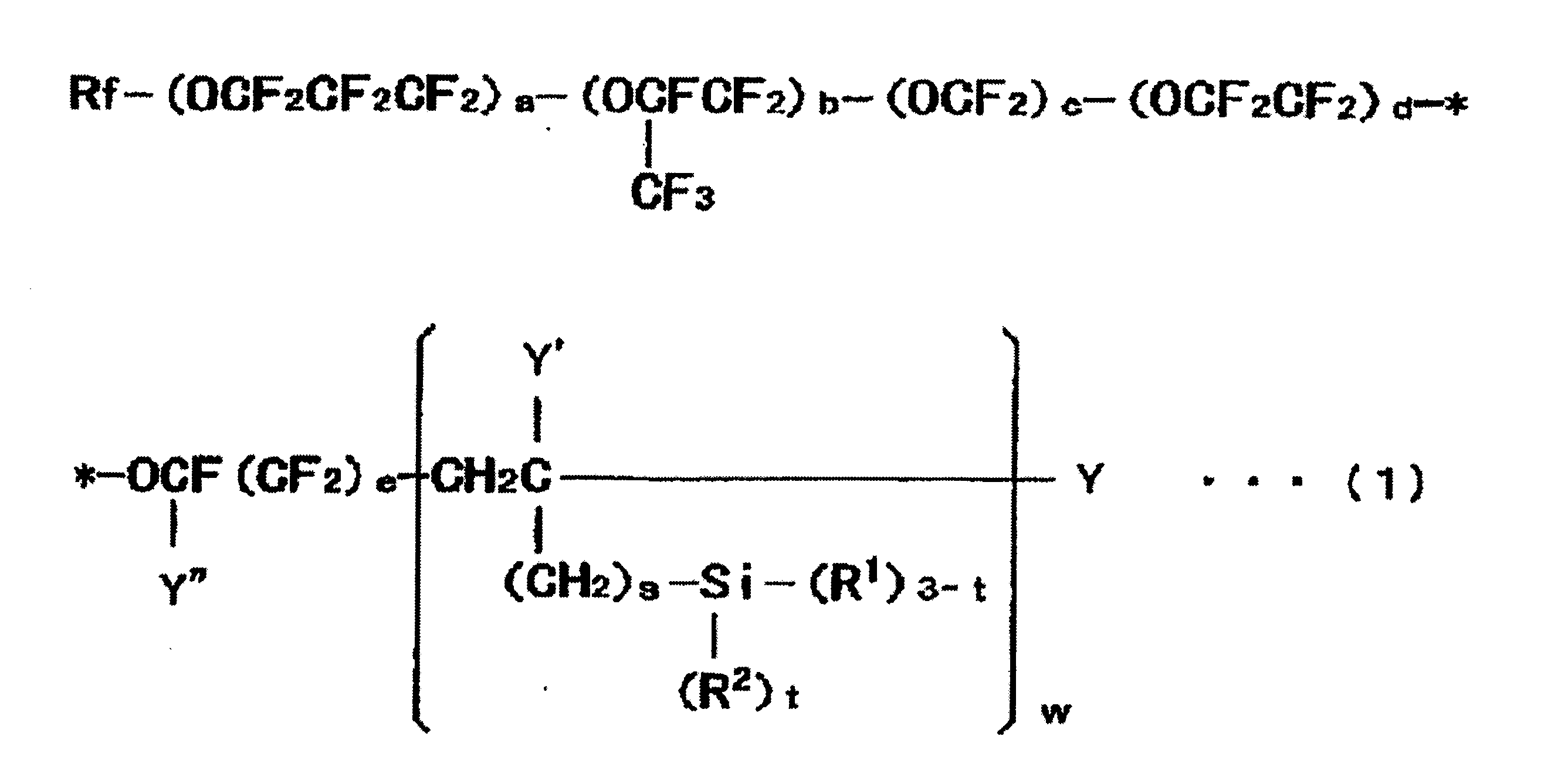
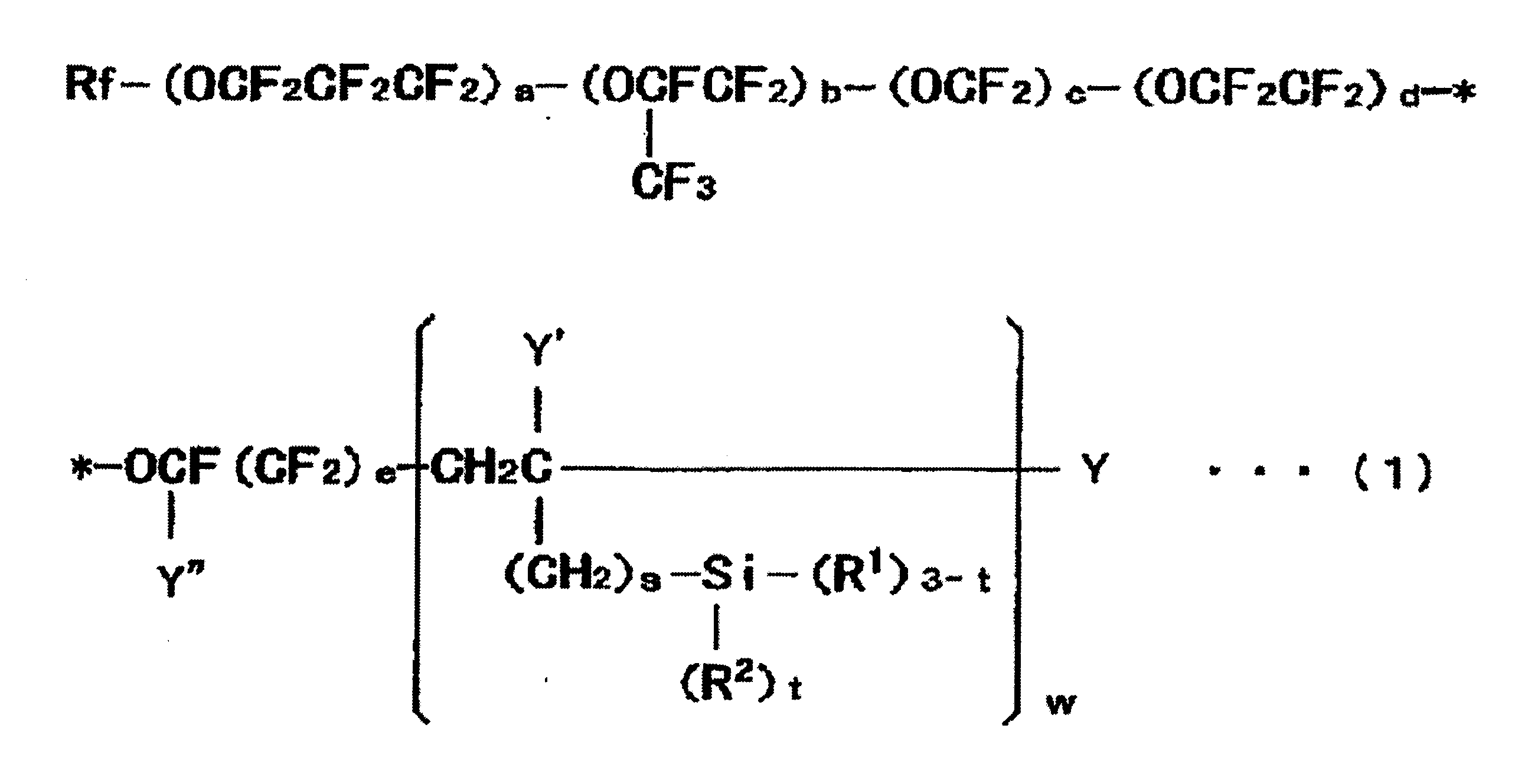
- the fluorine-substituted alkyl group-containing organosilicon compound the following general formula (1):
- Rf represents a linear or branched perfluoroalkyl group having 1 to 16 carbon atoms
- Y represents iodine or hydrogen
- Y ′ represents hydrogen or a lower alkyl group having 1 to 5 carbon atoms.
- Y ′′ represents a fluorine or trifluoromethyl group
- R 1 represents a hydrolyzable group
- R 2 represents hydrogen or an inert monovalent organic group
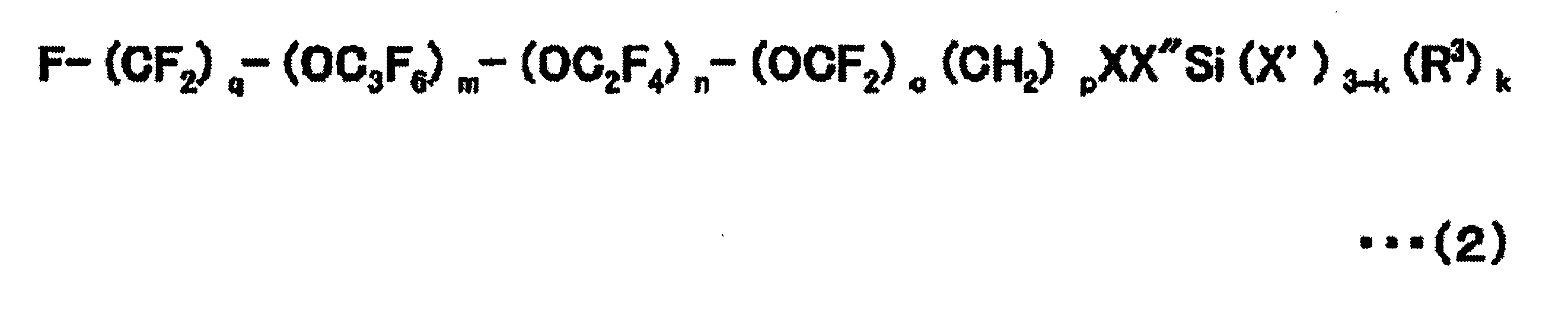
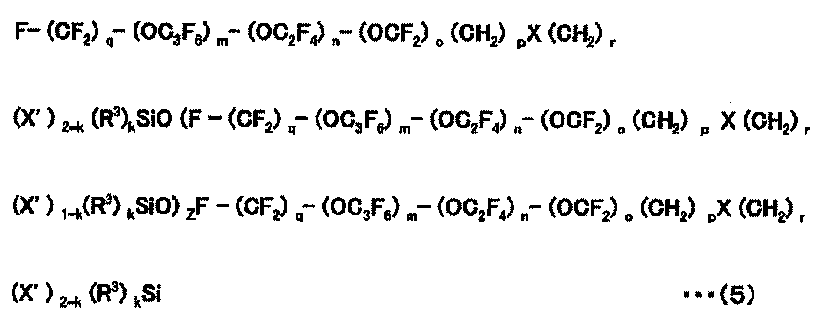
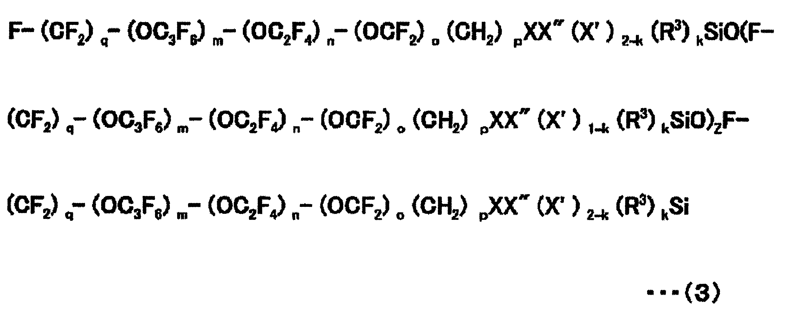
- a, b, c, d are Each represents an integer of 0 to 200, e represents 0 or 1, s and t each represents an integer of 0 to 2, and w represents an integer of 1 to 10) and the following general formulas (2) to ( 5):
- X represents oxygen or a divalent organic group
- X ′ represents a hydrolyzable group
- X ′′ represents a divalent organic silicone group
- R 3 represents carbon.
- q represents an integer of 1 to 3
- m, n and o each represents an integer of 0 to 200
- p represents 1 or 2
- r Represents an integer of 2 to 20
- k represents an integer of 0 to 2
- z represents an integer of 0 to 10 when k is 0 or 1
- Rf 2 represents a divalent linear perfluoropolyether group
- R 4 represents an alkyl group having 1 to 4 carbon atoms or a phenyl group
- R 5 represents a hydrolyzable group.
- I represents an integer of 0 to 2
- j represents an integer of 1 to 5
- u represents 2 or 3.
- a fluorine-substituted alkyl group-containing organosilicon compound selected from the general formulas (1) to (5) and the general formula (6) The selected fluorine-substituted alkyl group-containing organosilicon compound can be used in combination.
- the fluorine-substituted alkyl group-containing organosilicon compound represented by the general formulas (1) to (5) OPTOOL-DSX, OPTOOL-AES4, etc. manufactured by Daikin Industries, Ltd. can be used.
- As the fluorine-substituted alkyl group-containing organosilicon compound represented by the general formula (6) KY-130, KY-164 manufactured by Shin-Etsu Chemical Co., Ltd. can be used.
- the optical component 1 further includes an inorganic multilayer film 3 ′ disposed on two surfaces of the plastic substrate 2.
- a functional thin film 4 is disposed between the two surfaces of the plastic substrate 2 and the inorganic multilayer film 3 ′, as with the first surface.
- the inorganic multilayer film 3 ′ has a high refractive index layer 7 ′ having a multilayer structure in which a plurality of high refractive index inorganic materials and low refractive index inorganic materials are alternately laminated on the plastic substrate 2.
- On the 7 ' it is composed of a multilayer having a low refractive index layer 8' made of a low refractive index inorganic material having a lower refractive index than that of the high refractive index layer 7 '.
- the high refractive index layer 7 ′ includes a first layer 9 ′ made of a high refractive index inorganic material provided on the plastic substrate 2 side, and a low refractive index inorganic provided on the first layer 9 ′.
- a second layer 10 ′ made of a material and a third layer 11 ′ made of a high refractive index inorganic material provided on the second layer 10 ′.
- Inorganic materials used for the first layer 9 ′, the second layer 10 ′, and the third layer 11 ′ in the present embodiment include the first layer 9, the second layer 10, and the third layer 11 in the first embodiment.
- the thing similar to the inorganic material used is mentioned.
- the high refractive index layer 7 ′ can be composed of two layers or four or more layers without forming it in a three-layer structure, like the high refractive index layer 7 in the first embodiment.
- the functional thin film 4 is formed including the primer layer 5 and the hard coat layer 6.
- the primer layer 5 or the hard coat layer 6 is selected.
- One or both may be omitted.
- a dielectric film or a metal film made of ITO (Indium Tin Oxide) or the like may be provided in addition to the primer layer 5 and the hard coat layer 6.
- a dielectric film or a metal film having a thickness of 20 nm or less may be disposed between the high refractive index inorganic material and the low refractive index inorganic material constituting the inorganic multilayer film. Note that the thickness of the dielectric film or the metal film may be 10 nm or less.
- an inorganic multilayer film is used as the multilayer film, but an organic multilayer film may be used as long as the effects of the present invention are not impaired.
- any one of the both surfaces of the plastic substrate may be the front surface or the rear surface.
- one surface can be a front surface and two surfaces can be a rear surface.
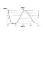
- FIG. 2 shows the relationship between the light wavelength and the reflectance of the inorganic multilayer film 3 (multilayer film disposed on one surface) or the inorganic multilayer film 3 ′ (multilayer film disposed on two surfaces) at the light wavelength.
- the spectral characteristic curve O1 showing the relationship between the wavelength range and the reflectance of the inorganic multilayer film 3 in the wavelength range has one (reflectance) maximum value (FIG. 2) in the wavelength range of 380 to 780 nm.
- the reflectance at the point X1 and one (reflectance) minimum value (the reflectance at the point X2 in FIG. 2) within the wavelength 200 nm from the wavelength corresponding to the maximum value (first wavelength). .
- the wavelength region is preferably 400 to 500 nm, more preferably 410 to 465 nm, and particularly preferably 430 to 450 nm.
- the average reflectance in the wavelength range of 25 nm before and after the wavelength corresponding to the maximum value (the wavelength at the point X1 in FIG. 2) (the wavelength range at the points X3 to X4 in FIG. 2) is 50% or less, and 20 % Or less, and more preferably 10% or less.
- the average reflectance of the inorganic multilayer film 3 ′ (multilayer film disposed on two surfaces) is 40% or less, preferably 20% or less, and more preferably 10% or less.
- the spectral characteristic curve O2 showing the relationship between the wavelength range and the reflectance of the inorganic multilayer film 3 ′ in the wavelength range corresponds to the maximum value of the spectral characteristic curve O1 (the reflectance at the point X1 in FIG. 2). There is no maximum value in the wavelength range of 25 nm before and after the wavelength (the wavelength range at point X3 to point X4 in FIG. 2).
- the spectral characteristic curve O1 showing the relationship between the wavelength and the reflectance with respect to the inorganic multilayer film 3 disposed on one surface of the plastic substrate 2 is the first wavelength in the wavelength range of 380 to 780 nm (in FIG. 2).
- the wavelength at the point X1) has one maximum value (reflectance at the point X1 in FIG. 2), and the second wavelength within 200 nm from the first wavelength (the wavelength at the point X2 in FIG. 2). It has one minimum value (reflectance at point X2 in FIG. 2), and the average reflectance in the wavelength range from the first wavelength to 25 nm before and after (wavelength range from point X3 to point X4 in FIG. 2) is 50% or less.
- the average reflectance of the inorganic multilayer film 3 ′ disposed on the two surfaces of the plastic substrate 2 is the average of the inorganic multilayer film 3 disposed on the one surface.
- the spectral characteristic curve O2 showing the relationship between the wavelength and the reflectance with respect to the inorganic multilayer film 3 ′ disposed on the two surfaces of the tic substrate 2 does not have a maximum value in the wavelength range of 25 nm before and after the first wavelength.
- the inorganic multilayer film 3 and the inorganic multilayer film 3 ′ have the above characteristics, generation of ghost light generated in the optical component can be suppressed.
- the inorganic multilayer film 3 and the inorganic multilayer film 3 ′ can have a property that satisfies the following conditions.
- n an integer of 1 or more.
- n an integer of 1 or more.
- Y of the tristimulus values XYZ is calculated from K, S ( ⁇ ), color matching function x ( ⁇ ) y ( ⁇ ) z ( ⁇ ), T gn ( ⁇ ), and the following equation (4). Find the value.
- the inorganic multilayer film 3 and the inorganic multilayer film 3 ′ are configured to have a Y value of 2.0 ⁇ 10 ⁇ 2 or less.
- the inorganic multilayer film 3 and the inorganic multilayer film 3 ′ have such a Y value, generation of ghost light generated in the optical component can be more effectively suppressed.
- the manufacturing method of the present embodiment includes a step of forming the functional thin film 4 (primer layer 5 and hard coat layer 6) on the plastic substrate 2 by a method similar to the conventional method, and a step of heating the plastic substrate 2. After the plastic substrate 2 is adjusted to a predetermined temperature (for example, 70 ° C.) by heating, the inorganic multilayer film 3 and the inorganic multilayer film 3 ′ are formed on both surfaces of the plastic substrate 2 consisting of one surface and two surfaces, respectively. And a step of forming a water / oil repellent film 12 on the inorganic multilayer film 3 and the inorganic multilayer film 3 ′.
- a predetermined temperature for example, 70 ° C.
- the step of forming the inorganic multilayer film 3 and the inorganic multilayer film 3 ′ is a process of forming a plurality of high refractive index layers 7 and 7 ′ having a multilayer structure by alternately laminating a plurality of high refractive index inorganic materials and low refractive index inorganic materials. And a process of forming low refractive index layers 8 and 8 'made of a low refractive index inorganic material on the high refractive index layers 7 and 7'. For example, a vacuum deposition method can be used for forming these layers.
- FIG. 3 is a diagram showing an example of a vapor deposition apparatus (film formation apparatus) 30 for forming each layer of the inorganic multilayer film 3.
- the vapor deposition apparatus 30 includes a first film formation chamber 31, a second film formation chamber 32, and a third film formation chamber 33.
- the first film forming chamber 31, the second film forming chamber 32, and the third film forming chamber 33 are configured so that the inside thereof is substantially decompressed to a vacuum and maintained in that state.
- the vapor deposition apparatus 30 can adjust the internal temperature of each of the first film forming chamber 31, the second film forming chamber 32, and the third film forming chamber 33 by temperature control means (not shown).
- the vapor deposition apparatus 30 includes a holding member 34 in each internal space of the first film formation chamber 31, the second film formation chamber 32, and the third film formation chamber 33.
- the holding member 34 has a curved upper surface (holding surface) and is configured to be rotatable, and holds a plurality of plastic substrates 2 on the upper surface.
- the vapor deposition source 35 of the vapor deposition apparatus 30 is disposed in a space inside the second film formation chamber 32.
- the vapor deposition source 35 includes a first vapor deposition source 35A and a second vapor deposition source 35B.
- a light source device 36 capable of irradiating the vapor deposition source 35 with a beam is disposed.
- the light source device 36 can strike the constituent particles of the vapor deposition source 35 by irradiating the vapor deposition source 35 with electrons.
- a material (gas) for forming the inorganic multilayer film 3 and the inorganic multilayer film 3 ′ is emitted from the vapor deposition source 35.
- the light source device 36 irradiates the first vapor deposition source 35A with a beam
- the vapor of ZrO 2 is discharged from the first vapor deposition source 35A, and is supplied onto the plastic substrate 2 held by the holding member 34 for vapor deposition.
- the second vapor deposition source 35B by irradiating the second vapor deposition source 35B with a beam, SiO 2 vapor is released from the second vapor deposition source 35B, and is supplied onto the plastic substrate 2 held by the holding member 34 for vapor deposition.
- the second layers 10 and 10 ′ and the low refractive index layers 8 and 8 ′ in the high refractive index layers 7 and 7 ′ of the inorganic multilayer film 3 and the inorganic multilayer film 3 ′ can be formed.
- the optical component according to the embodiment of the present invention is a spectroscope that shows the relationship between the wavelength range and the reflectance of the multilayer film (inorganic multilayer film 3) disposed on one surface of the plastic substrate 2 in the wavelength range.
- the characteristic curve has one maximum value in the wavelength range of 380 to 780 nm and one minimum value at the second wavelength within 200 nm from the wavelength corresponding to the maximum value (first wavelength) on the long wavelength side.
- the wavelength corresponding to the maximum value (first wavelength) is set so that the average reflectance of the multilayer film disposed on one surface of the plastic substrate 2 in the wavelength range of 25 nm before and after the wavelength corresponding to the value is 50% or less.
- the average reflectance of the multilayer film (inorganic multilayer film 3 ') disposed on the two surfaces of the plastic substrate 2 in the wavelength range of 25 nm from the front to the back is 40 of the average reflectance of the multilayer film disposed on the one surface.
- the spectral characteristic curve showing the relationship with the reflectance of the multilayer film disposed on the two surfaces of the plastic substrate 2 in the wavelength range does not have a maximum value in the wavelength range of 25 nm before and after the wavelength corresponding to the maximum value.
- a vapor deposition source made of zirconium oxide (ZrO) was used as the first vapor deposition source 35A, and the first vapor deposition source 35A was irradiated with a beam while introducing oxygen into the internal space of the second film formation chamber 32, so that zirconium dioxide (ZrO You may make it form the high refractive index inorganic material layer which consists of 2 ).
- the step of forming the inorganic multilayer film 3 and the inorganic multilayer film 3 ′ includes at least one of the layers constituting the inorganic multilayer film 3 and the inorganic multilayer film 3 ′.
- a step of forming a film while performing ion beam assist may be included.
- a dielectric film is disposed between the high refractive index inorganic material and the low refractive index inorganic material constituting the inorganic multilayer film. .
- FIG. 4 is a diagram illustrating an example of a film forming apparatus 30 ′ for performing ion beam assist.
- the film forming apparatus 30 ′ has a configuration in which an ion gun 37 is provided in the second film forming chamber of the vapor deposition apparatus 30 shown in FIG.
- a dielectric film such as ITO is disposed between the high refractive index layers 7 and 7 ′ and the low refractive index layers 8 and 8 ′ constituting the inorganic multilayer film 3 and the inorganic multilayer film 3 ′.
- film formation is performed while performing ion beam assist.
- At least one of the layers constituting the inorganic multilayer film 3 in the second film forming chamber 32 may be formed while performing ion beam assist, and the target to be subjected to ion beam assist is limited to the dielectric film. Not.
- the second film forming chamber of the film forming apparatus 30 ′ includes a holding member 34 that holds the base material on which the high refractive index layers 7 and 7 ′ are formed on the plastic base material 2, and a vapor deposition source. 35 ', an ion gun 37 that is spaced apart from the vapor deposition source 35', and a light source device 36. Further, the film forming apparatus 30 ′ is configured so that the inside thereof is substantially decompressed to a vacuum, and the periphery of the plastic substrate 2 can be maintained in a vacuum atmosphere.
- an atmospheric gas supply source such as a gas cylinder is connected to the film forming apparatus 30 ′, and the inside of the vacuum vessel is in a low pressure state such as a vacuum, and an oxygen gas, argon gas, or other inert gas atmosphere, Or it is comprised so that it can be set as the inert gas atmosphere containing oxygen.
- the vapor deposition source 35 ' includes, for example, ITO.
- ITO indium gallium tin oxide
- the gasified ITO is emitted from the vapor deposition source 35 ′ and supplied to the plastic substrate 2 held by the holding member 34.
- a dielectric film made of ITO can be formed on the high refractive index layers 7 and 7 ′.
- the ion gun 37 includes a gas introduction part for introducing a gas to be ionized inside the second film forming chamber 32 and a lead electrode on the front.
- the ion gun 37 is a device that ionizes a part of gas atoms or molecules, and irradiates the ionized particles as an ion beam by controlling with an electric field generated by an extraction electrode.
- the light source device 36 has a configuration equivalent to that of the ion gun 37, and can irradiate electrons to the vapor deposition source 35 'to knock out the constituent particles of the vapor deposition source 35'.
- a voltage is applied to the vapor deposition source 35 ′ with a high-frequency coil or the like to form the constituent particles of the vapor deposition source 35 ′.
- the light source device 36 may be omitted.
- an ITO dielectric film is formed on the high refractive index layers 7 and 7 ′ on the plastic substrate 2 using the film forming apparatus 30 ′ having the above-described configuration.
- an ITO vapor deposition source 35 ′ is used, and ions irradiated from the ion gun 37 can be irradiated onto the upper surface of the holding member 34.
- the inside of the film forming chamber 32 containing the plastic substrate 2 is evacuated to make a reduced pressure atmosphere. Then, the ion gun 37 and the light source device 36 are operated.
- the constituent particles of the vapor deposition source 35' are knocked out and fly onto the high refractive index layers 7 and 7 '. Then, on the high refractive index layers 7 and 7 ′, the constituent particles knocked out from the vapor deposition source 35 ′ are deposited, and at the same time, argon ions are irradiated from the ion gun 37 as an ion beam.
- ion beam assist is performed using at least one gas selected from an inert gas, an oxygen gas, and a mixed gas of an inert gas and an oxygen gas.
- argon can be used as the inert gas.
- the water / oil repellent film 12 is formed thereon.
- a wet method such as a dipping method, a spin coat method and a spray method, or a dry method such as a vacuum deposition method.
- the dipping method is common and is often used.
- the optical component formed up to the inorganic multilayer films 3 and 3 ′ is immersed in a solution obtained by dissolving a fluorine-substituted alkyl group-containing organosilicon compound in an organic solvent, and the film is formed by pulling up and drying under certain conditions. It is.
- the organic solvent perfluorohexane, perfluoro-4-methoxybutane, perfluoro-4-ethoxybutane, metaxylene hexafluoride, or the like is used.
- the dilution concentration with the organic solvent can be 0.01 to 0.5% by weight, preferably 0.03 to 0.1% by weight. If the concentration is too low, the water / oil repellent layer 12 having a sufficient film thickness may not be obtained. If the concentration is too high, uneven coating tends to occur and the material cost may increase. Of the dry methods, vacuum deposition is often used. This method is a method of forming the water- and oil-repellent film 12 by heating and evaporating the fluorine-substituted alkyl group-containing organosilicon compound in a vacuum chamber.
- the inorganic multilayer film 3 and the inorganic multilayer film 3 ′ are designed so as to have the above-described characteristics, so that the generation of ghost light generated in the optical component can be suppressed.
- the method of manufacturing an optical component such a well-balanced and excellent optical component can be reliably provided.
- the ghost light quantification method of this embodiment is a method of multiply reflecting light within an optical component including a plastic substrate 2 and a multilayer film disposed on both sides of the plastic substrate 2.
- n an integer of 1 or more.
- n an integer of 1 or more.
- the obtained Y value is defined as the intensity of ghost light.
- the present inventor has found a method for quantifying the intensity of ghost light generated in an optical component. Reduction of ghost light by using the method according to the embodiment of the present invention and setting, for example, a Y value of 2.0 ⁇ 10 ⁇ 2 or less as a reference for a multilayer film disposed in an optical component Can be manufactured.
- the optical thickness is 0.060 ⁇
- the fifth layer ZrO 2 (refractive index 2.00) is the optical thickness 0.190 ⁇
- the sixth layer SiO 2 (refractive index 1.47) is the optical thickness 0.340 ⁇ .
- ⁇ is 500 nm as the design center wavelength.
- 2 side Using the same apparatus as for 1 side, after pre-processing in the same processing atmosphere, the first layer ZrO 2 (refractive index 2.00) is sequentially applied to the optical film thickness of 0.050 ⁇ from the plastic substrate side.
- the second layer SiO 2 (refractive index 1.47) has an optical film thickness of 0.080 ⁇
- the third layer ZrO 2 (refractive index 2.00) has an optical film thickness of 0.150 ⁇
- the fourth layer SiO 2 (refractive index).
- the refractive index 1.47) is the optical film thickness 0.040 ⁇
- the fifth layer ZrO 2 (refractive index 2.00) is the optical film thickness 0.110 ⁇
- the sixth layer SiO 2 (refractive index 1.47) is optical.
- Lamination was performed with a film thickness of 0.220 ⁇ . Note that ⁇ is 500 nm as the design center wavelength.
- FIG. 5A shows the spectral characteristics on one surface of the lens of Example 1.
- FIG. Numerical data of the spectral characteristics of FIG. 5A is shown in FIG. 5B.
- FIG. 6A shows the spectral characteristics of the two surfaces of the lens of Example 1.
- FIG. Numerical data of the spectral characteristics of FIG. 6A is shown in FIG. 6
- the optical thickness is 0.500 ⁇
- the fifth layer ZrO 2 (refractive index 2.00) is the optical thickness 0.170 ⁇
- the sixth layer SiO 2 (refractive index 1.47) is the optical thickness 0.110 ⁇ .
- the seventh layer ZrO 2 (refractive index 2.00) has an optical thickness of 0.190 ⁇
- the eighth layer SiO 2 (bending A refractive index of 1.47) was laminated with an optical film thickness of 0.280 ⁇ . Note that ⁇ is 500 nm as the design center wavelength.
- 2 side Using the same apparatus as that for 1 side, after pre-processing in the same processing atmosphere, the first layer ZrO 2 (refractive index 2.00) is sequentially applied to the optical film thickness of 0.110 ⁇ from the plastic substrate side.
- the second layer SiO 2 (refractive index 1.47) has an optical thickness of 0.090 ⁇
- the third layer ZrO 2 (refractive index 2.00) has an optical thickness of 0.220 ⁇
- the fourth layer SiO 2 (refractive index).
- the refractive index 1.47) is the optical film thickness 0.060 ⁇
- the fifth layer ZrO 2 (refractive index 2.00) is the optical film thickness 0.200 ⁇
- the sixth layer SiO 2 (refractive index 1.47) is optical.
- Lamination was performed with a film thickness of 0.330 ⁇ . Note that ⁇ is 500 nm as the design center wavelength.
- FIG. 7A shows the spectral characteristics on one surface of the lens of Example 2.
- FIG. Numerical data of the spectral characteristics of FIG. 7A is shown in FIG. 7B.
- the spectral characteristics of the two surfaces of the lens of Example 2 are shown in FIG. 8A.
- Numerical data of the spectral characteristics of FIG. 8A is shown in FIG. 8B
- the optical thickness is 0.060 ⁇
- the fifth layer ZrO 2 (refractive index 2.00) is the optical thickness 0.160 ⁇
- the sixth layer SiO 2 (refractive index 1.47) is the optical thickness 0.340 ⁇ .
- ⁇ is 500 nm as the design center wavelength.
- 2 side Using the same apparatus as for 1 side, after pre-processing in the same processing atmosphere, the first layer ZrO 2 (refractive index 2.00) is sequentially applied to the optical film thickness of 0.070 ⁇ from the plastic substrate side.
- the second layer SiO 2 (refractive index 1.47) has an optical film thickness of 0.070 ⁇
- the third layer ZrO 2 (refractive index 2.00) has an optical film thickness of 0.140 ⁇
- the fourth layer SiO 2 (refractive index).
- the optical thickness is 0.050 ⁇
- the fifth layer ZrO 2 (refractive index 2.00) is the optical thickness 0.120 ⁇
- the sixth layer SiO 2 (refractive index 1.47) is the optical thickness.
- the layers were laminated with a film thickness of 0.290 ⁇ . Note that ⁇ is 500 nm as the design center wavelength.
- FIG. 9A shows the spectral characteristics on one surface of the lens of Example 3.
- FIG. 9B The numerical data of the spectral characteristics of FIG. 9A is shown in FIG. 9B.
- FIG. 10A shows the spectral characteristics of the two surfaces of Example 3.
- FIG. 10B The numerical data of the spectral characteristics of FIG. 10A is shown in FIG. 10B.
- the optical thickness is 0.060 ⁇
- the fifth layer ZrO 2 (refractive index 2.00) is the optical thickness 0.160 ⁇
- the sixth layer SiO 2 (refractive index 1.47) is the optical thickness 0.340 ⁇ .
- ⁇ is 500 nm as the design center wavelength.
- 2 side Using the same apparatus as for 1 side, after pre-processing in the same processing atmosphere under the same processing atmosphere, the first layer ZrO 2 (refractive index 2.00) is sequentially applied from the plastic substrate side to the optical film thickness of 0.100 ⁇ .
- the second layer SiO 2 (refractive index 1.47) has an optical film thickness of 0.100 ⁇
- the third layer ZrO 2 (refractive index 2.00) has an optical film thickness of 0.200 ⁇
- the fourth layer SiO 2 (refractive index).
- the refractive index 1.47) is the optical film thickness 0.060 ⁇
- the fifth layer ZrO 2 (refractive index 2.00) is the optical film thickness 0.160 ⁇
- the sixth layer SiO 2 (refractive index 1.47) is optical.
- Lamination was performed with a film thickness of 0.340 ⁇ . Note that ⁇ is 500 nm as the design center wavelength.
- FIG. 11A shows numerical data of the spectral characteristics of FIG. 11A.
- the optical thickness is 0.550 ⁇
- the fifth layer ZrO 2 (refractive index 2.00) is the optical thickness 0.160 ⁇
- the sixth layer SiO 2 (refractive index 1.47) is the optical thickness 0.090 ⁇ .
- the seventh layer ZrO 2 (refractive index 2.00) has an optical film thickness of 0.200 ⁇ and the eighth layer SiO 2 (bending A refractive index of 1.47) was laminated with an optical film thickness of 0.310 ⁇ . Note that ⁇ is 500 nm as the design center wavelength.
- 2 side Using the same apparatus as that for 1 side, after pre-processing in the same processing atmosphere, the first layer ZrO 2 (refractive index 2.00) is sequentially applied to the optical film thickness of 0.150 ⁇ from the plastic substrate side.
- the second layer SiO 2 (refractive index 1.47) has an optical film thickness of 0.050 ⁇
- the third layer ZrO 2 (refractive index 2.00) has an optical film thickness of 0.170 ⁇
- the fourth layer SiO 2 (refractive index).
- the refractive index 1.47) is the optical film thickness 0.550 ⁇
- the fifth layer ZrO 2 (refractive index 2.00) is the optical film thickness 0.160 ⁇
- the sixth layer SiO 2 (refractive index 1.47) is optical.
- an eighth layer SiO 2 (refractive index 1.47) with an optical thickness of 0.310 ⁇ were laminated. .
- ⁇ is 500 nm as the design center wavelength.
- the spectral characteristics on both surfaces of the lens of Comparative Example 2 are shown in FIG. 12A.
- Numerical data of the spectral characteristics of FIG. 12A is shown in FIG. 12
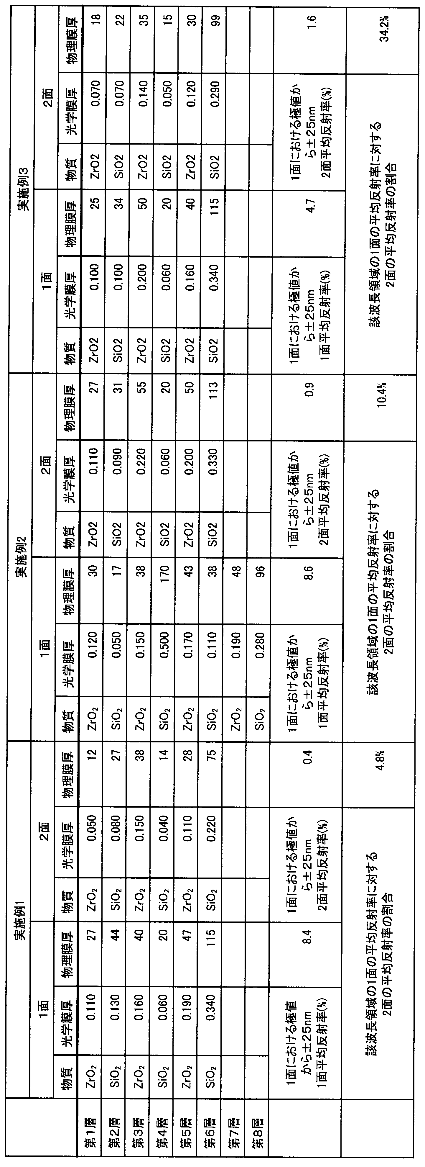
- Tables 1 and 2 show details of the respective film formation layers in Examples 1 to 3 and Comparative Examples 1 and 2.
- n an integer of 1 or more.
- n an integer of 1 or more.
- the Y value of the tristimulus values XYZ is calculated according to JIS 8701, with the relative spectral intensity of the standard light source (D65) as S ( ⁇ ) and the color matching function as x ( ⁇ ) y ( ⁇ ) z ( ⁇ ). Y is
- This Y value was used as a ghost light intensity for quantitative comparative evaluation. Further, in the spectral characteristic curve, the sum of the average reflectance of one surface in the wavelength range of 25 nm before and after the wavelength at which the reflectance of one surface exhibits an extreme value (first wavelength) and the average reflectance of the two surfaces in this wavelength range. was calculated. The results are shown in Table 3.
- Example 1 the ghost light was reduced by 40% in spite of the fact that the average reflectance in the above wavelength range was maintained at the same level as in Comparative Example 1. Similarly, when Example 3 was compared with Comparative Example 1, it was confirmed that Example 3 reduced ghost light by 63%. Furthermore, when Example 2 and Comparative Example 2 were compared, it was confirmed that Example 2 reduced ghost light by 72%. Furthermore, wearing evaluation was performed using these optical components.
- an optical component that has an antiglare effect, reduces fatigue, is effective in preventing eye disease, and has a relatively high reflection and good visibility.
- SYMBOLS 1 Optical component, 2 ... Plastic base material, 3, 3 '... Inorganic multilayer film, 4 ... Functional thin film, 5 ... Primer layer (functional thin film), 6 ... Hard-coat layer (functional thin film), 7, 7 '... high refractive index layer, 8, 8' ... low refractive index layer, 9, 9 '... first layer, 10, 10' ... second layer, 11, 11 '... third layer, 12 ... water / oil repellent film 30 ... deposition device, 30 '... deposition device, 31 ... first deposition chamber, 32 ... second deposition chamber, 33 ... third deposition chamber, 34 ... holding member, 35, 35' ... deposition source, 35A ... first vapor deposition source, 35B ... second vapor deposition source, 36 ... light source device, 37 ... ion gun.
Landscapes
- Physics & Mathematics (AREA)
- General Physics & Mathematics (AREA)
- Optics & Photonics (AREA)
- Health & Medical Sciences (AREA)
- Ophthalmology & Optometry (AREA)
- General Health & Medical Sciences (AREA)
- Chemical & Material Sciences (AREA)
- Chemical Kinetics & Catalysis (AREA)
- Surface Treatment Of Optical Elements (AREA)
- Laminated Bodies (AREA)
- Eyeglasses (AREA)
- Optical Filters (AREA)
Abstract
Description
本願は、2012年11月5日に出願された特願2012-243956号に基づき優先権を主張し、その内容をここに援用する。
また、目の健康に対して、可視光線の青色領域(380~500nm)はエネルギーが強いため、網膜などに好ましくない影響を与える原因になると言われている。
しかし、この方法では多層膜の反射率が高く、レンズ内で強い多重反射を起こし、鮮明なゴースト光が視界に入ってしまう可能性がある。




また、本発明の態様に係る光学部品の製造方法によれば、レンズ内の多重反射を軽減し、見え易く、疲労、眼病予防にも効果的な光学特性を有した光学部品を提供することが可能となる。
なお、この形態は、発明の趣旨をより良く理解させるために具体的に説明するものであり、特に指定のない限り、本発明を限定するものではない。
図1は、本発明の実施形態に係る光学部品を模式的に示す側断面図である。図1において符号1は眼鏡レンズ用の光学部品である。
光学部品1は、プラスチック基材2と、プラスチック基材2の1面に配設された無機多層膜3とを備えている。プラスチック基材2の1面と無機多層膜3との間には、本実施形態では機能性薄膜4が配設されている。機能性薄膜4は、本実施形態ではプライマー層5とハードコート層6とからなっている。
また、本実施形態では、プラスチック基材2の屈折率(nd)としては、例えば1.50、1.60、1.67、及び1.74のうちから選択されたものが用いられる。なお、プラスチック基材2の屈折率を1.6以上にする場合、プラスチック基材2としては、アリルカーボネート系樹脂、アクリレート系樹脂、メタクリレート系樹脂、及びチオウレタン系樹脂等を使用することができる。
また、プラスチック基材2は透光性を有していれば透明でなくてもよく、着色されていてもよい。着色されたプラスチック基材2の透過率は、5~85%とすることができる。
プライマー層5は、プラスチック基材2とハードコート層6との密着性を良好にするためのもので、密着層として機能するようになっている。また、光学部品1に対する衝撃を吸収するためのものでもあり、衝撃吸収層としても機能するようになっている。
ハードコート層6は、例えばオルガノシロキサン系ハードコート層からなっている。オルガノシロキサン系ハードコート層は、オルガノシロキサン系樹脂に無機酸化物の微粒子を分散させたものである。無機酸化物としては、例えばルチル型の酸化チタンや、ケイ素、錫、ジルコニウム、及びアンチモンの酸化物が用いられる。また、ハードコート層6として、例えば特公平4-55615号公報に開示されているような、コロイド状シリカ含有の有機ケイ素系樹脂であってもよい。ハードコート層6の厚み(実際の厚み)は、2μm以上4μm以下程度とすることができる。
また、本実施形態において、無機多層膜を構成する高屈折率無機材料と低屈折率無機材料との間に、厚さ20nm以下の誘電体膜又は金属膜を配設してもよい。なお、誘電体膜又は金属膜の厚さは、10nm以下であってもよい。
また、高屈折率層7については、上記のように第1層9、第2層10、第3層11の3層構造で形成することなく、上述した反射率についての条件を満たせば、2層、または4層以上で構成することもできる。
撥水撥油膜12は、フッ素置換アルキル基含有有機ケイ素化合物を主成分とするもので、撥液性(撥水性、撥油性)を有するものである。すなわち、撥水撥油膜12は、光学部品の表面エネルギーを低下させ、水やけ防止、汚れ防止の機能を発揮するとともに、光学部品表面のすべり性能を向上させ、その結果として、耐擦傷性を向上させることができる。
フッ素置換アルキル基含有有機ケイ素化合物としては、下記一般式(1):



一般式(1)~(5)で示されるフッ素置換アルキル基含有有機ケイ素化合物としては、ダイキン工業株式会社製オプツール-DSX、オプツール-AES4などを用いることができる。また、一般式(6)で示されるフッ素置換アルキル基含有有機ケイ素化合物としては、信越化学工業株式会社製KY-130、KY-164などを用いることができる。
本実施形態における第1層9’、第2層10’、第3層11’に用いられる無機材料としては、第一の実施形態における第1層9、第2層10、第3層11に用いられる無機材料と同様のものが挙げられる。
高屈折率層7’については、第一の実施形態における高屈折率層7と同様に、三層構造で形成することなく、二層、または四層以上で構成することもできる。
また、本実施形態において、無機多層膜を構成する高屈折率無機材料と低屈折率無機材料との間に、厚さ20nm以下の誘電体膜又は金属膜を配設してもよい。なお、誘電体膜又は金属膜の厚さは、10nm以下であってもよい。
また、本実施形態においては、多層膜として無機多層膜を用いているが、本発明の効果を損なわない限り、有機多層膜を用いてもよい。
本実施形態において、波長範囲と、その波長範囲における無機多層膜3の反射率との関係を示す分光特性曲線O1は、380~780nmの波長範囲に、一つの(反射率)極大値(図2中、点X1における反射率)と、その極大値に対応する波長(第1波長)から長波長側200nm以内に一つの(反射率)極小値(図2中、点X2における反射率)を有する。点X1について、例えば青色光の好ましくない影響を有効に低減することを目的とした場合、その波長領域は、400~500nmが好ましく、410~465nmがより好ましく、430~450nmが特に好ましい。
更に、極大値に対応する波長(図2中、点X1における波長)から前後25nmの波長範囲(図2中、点X3~点X4における波長範囲)における平均反射率が50%以下であり、20%以下であることが好ましく、10%以下であることがより好ましい。
図2では、プラスチック基材2の1面に配設された無機多層膜3に関して波長と反射率との関係を示す分光特性曲線O1が、380~780nmの波長範囲における第1波長(図2中、点X1における波長)で一つの極大値(図2中、点X1における反射率)を有するとともに、第1波長から長波長側200nm以内の第2波長(図2中、点X2における波長)に一つの極小値(図2中、点X2における反射率)を有し、第1波長から前後25nmの波長範囲(図2中、点X3~点X4における波長範囲)における平均反射率が50%以下であり、第1波長から前後25nmの波長範囲において、プラスチック基材2の2面に配設された無機多層膜3’の平均反射率が、1面に配設された無機多層膜3の平均反射率の40%以下であり、プラスチック基材2の2面に配設された無機多層膜3’に関して波長と反射率との関係を示す分光特性曲線O2が、第1波長から前後25nmの波長範囲において、極大値を有しない。




次に、光学部品1の実施形態に基づき、本発明の光学部品の製造方法の一実施形態について説明する。
本実施形態の製造方法は、プラスチック基材2に対して従来と同様の方法で機能性薄膜4(プライマー層5、ハードコート層6)を形成する工程と、プラスチック基材2を加熱する工程と、加熱によってプラスチック基材2を所定温度(例えば70℃)に調整した後、このプラスチック基材2の1面と2面からなる両面に、無機多層膜3及び無機多層膜3’をそれぞれ形成する工程と、無機多層膜3及び無機多層膜3’上に撥水撥油膜12を形成する工程と、を備える。
光源装置36から射出された電子が蒸着源35に照射されることによって、蒸着源35から、無機多層膜3及び無機多層膜3’を形成するための材料(ガス)が放出される。
例えば、光源装置36が第1蒸着源35Aにビームを照射することにより、ZrO2の蒸気を第1蒸着源35Aから放出させ、保持部材34に保持されているプラスチック基材2上に供給し蒸着させる。これにより、無機多層膜3及び無機多層膜3’の高屈折率層7,7’における第1層9,9’と第3層11,11’を形成することができる。同様に、第2蒸着源35Bにビームを照射することにより、SiO2の蒸気を第2蒸着源35Bから放出させ、保持部材34に保持されているプラスチック基材2上に供給し蒸着させる。これにより、無機多層膜3及び無機多層膜3’の高屈折率層7,7’における第2層10,10’と、低屈折率層8,8’を形成することができる。
ただし、本発明の実施形態に係る光学部品は、波長範囲と、その波長範囲におけるプラスチック基材2の1面に配設された多層膜(無機多層膜3)の反射率との関係を示す分光特性曲線が、380~780nmの波長範囲に、一つの極大値と、その極大値に対応する波長(第1波長)から長波長側200nm以内の第2波長に一つの極小値を有し、極大値に対応する波長から前後25nmの波長範囲におけるプラスチック基材2の1面に配設された多層膜の平均反射率が50%以下となるようにし、極大値に対応する波長(第1波長)から前後25nmの波長範囲において、プラスチック基材2の2面に配設された多層膜(無機多層膜3’)の平均反射率が、1面に配設された多層膜の平均反射率の40%以下となるようにし、波長範囲と、その波長範囲におけるプラスチック基材2の2面に配設された多層膜の反射率との関係を示す分光特性曲線が、極大値に対応する波長から前後25nmの波長範囲において、極大値を有しないように設計する。
なお、第1蒸着源35Aとして酸化ジルコニウム(ZrO)からなる蒸着源を用い、第2成膜室32の内部空間に酸素を導入しながら第1蒸着源35Aにビームを照射し、二酸化ジルコニウム(ZrO2)からなる高屈折率無機材料層を形成するようにしてもよい。
本実施形態においては、無機多層膜3及び無機多層膜3’を構成する高屈折率層7,7’と低屈折率層8,8’との間に、ITO等の誘電体膜を配設する際に、イオンビームアシストを施しながら成膜を行う。
なお、第2成膜室32内で無機多層膜3を構成する層のうち少なくとも一層を、イオンビームアシストを施しながら成膜を行えばよく、イオンビームアシストを施す対象は、誘電体膜に限定されない。
また、成膜装置30’はその内部が実質的に真空に減圧され、プラスチック基材2の周囲を真空雰囲気に保持できるように構成されている。更に成膜装置30’には、ガスボンベ等の雰囲気ガス供給源が接続されていて、真空容器の内部を真空等の低圧状態で、かつ、酸素ガス、アルゴンガス、またはその他の不活性ガス雰囲気、あるいは、酸素を含む不活性ガス雰囲気にすることができるように構成されている。
光源装置36から蒸着源35’に電子を照射すると、蒸着源35’の構成粒子が叩き出されて高屈折率層7,7’上に飛来する。そして、高屈折率層7,7’上に、蒸着源35’から叩き出した構成粒子を堆積させると同時に、イオンガン37からアルゴンイオンをイオンビームとして照射する。
撥水撥油膜12の形成方法としては、ディッピング法、スピンコート法、スプレー法などの湿式法、あるいは真空蒸着法などの乾式法がある。
湿式法の中では、ディッピング法が一般的であり、よく用いられる。この方法は、フッ素置換アルキル基含有有機ケイ素化合物を有機溶剤に溶解した液中に、無機多層膜3,3’まで形成した光学部品を浸漬し、一定条件で引き上げ、乾燥させて成膜する方法である。
有機溶剤としては、パーフルオロヘキサン、パーフルオロ-4-メトキシブタン、パーフルオロ-4-エトキシブタン、メタキシレンヘキサフルオライドなどが使用される。
乾式法の中では、真空蒸着法がよく用いられる。この方法は、フッ素置換アルキル基含有有機ケイ素化合物を真空槽内で加熱して蒸発させ、撥水撥油膜12を形成する方法である。
また、光学部品の製造方法にあっては、このようなバランスのとれた優れた光学部品を確実に提供することができる。
次に、上記光学部品1の説明に基づき、本実施形態のゴースト光の定量方法について説明する。
本実施形態のゴースト光の定量方法は、プラスチック基材2と、プラスチック基材2の1面と2面からなる両面に配設された多層膜とを備えた光学部品内で、光の多重反射により生じるゴースト光の定量方法であって、1面に配設された多層膜の分光反射率R1(λ)[%]と、2面に配設された多層膜の分光反射率R2(λ)[%]と、以下の式(1)とから、An(λ)を求め、




ウレタン系合成樹脂基板上に、屈折率1.67のシリコン系ハードコート、及び屈折率1.67のプライマーコートを加熱硬化にて施し、以下に示すように真空蒸着法により成膜した。
1面:レンズを真空槽内に設けられた回転するドームにセットし、真空槽内の温度を70度に加熱し、圧力が1.0×10⁻³Paになるまで排気し、加速電圧500V、加速電流100mAの条件でArイオンビームクリーニングを60秒間施した後、プラスチック基材側から順次、第1層ZrO2(屈折率2.00)を光学的膜厚0.110λ、第2層SiO2(屈折率1.47)を光学的膜厚0.130λ、第3層ZrO2(屈折率2.00)を光学的膜厚0.160λ、第4層SiO2(屈折率1.47)を光学的膜厚0.060λ、第5層ZrO2(屈折率2.00)を光学的膜厚0.190λ、第6層SiO2(屈折率1.47)を光学的膜厚0.340λで積層した。尚、λは設計の中心波長で500nmとした。
2面:1面と同様の装置を用いて、同様の加工雰囲気下で前処理後、プラスチック基材側から順次、第1層ZrO2(屈折率2.00)を光学的膜厚0.050λ、第2層SiO2(屈折率1.47)を光学的膜厚0.080λ、第3層ZrO2(屈折率2.00)を光学的膜厚0.150λ、第4層SiO2(屈折率1.47)を光学的膜厚0.040λ、第5層ZrO2(屈折率2.00)を光学的膜厚0.110λ、第6層SiO2(屈折率1.47)を光学的膜厚0.220λで積層した。尚、λは設計の中心波長で500nmとした。
実施例1のレンズの1面における分光特性を図5Aに示す。図5Aの分光特性の数値データを図5Bに示す。実施例1のレンズの2面における分光特性を図6Aに示す。図6Aの分光特性の数値データを図6Bに示す。
1面:レンズを真空槽内に設けられた回転するドームにセットし、真空槽内の温度を70度に加熱し、圧力が1.0×10⁻³Paになるまで排気し、加速電圧500V、加速電流100mAの条件でArイオンビームクリーニングを60秒間施した後、プラスチック基材側から順次、第1層ZrO2(屈折率2.00)を光学的膜厚0.120λ、第2層SiO2(屈折率1.47)を光学的膜厚0.050λ、第3層ZrO2(屈折率2.00)を光学的膜厚0.150λ、第4層SiO2(屈折率1.47)を光学的膜厚0.500λ、第5層ZrO2(屈折率2.00)を光学的膜厚0.170λ、第6層SiO2(屈折率1.47)を光学的膜厚0.110λ、第7層ZrO2(屈折率2.00)を光学的膜厚0.190λ、第8層SiO2(屈折率1.47)を光学的膜厚0.280λで積層した。尚、λは設計の中心波長で500nmとした。
2面:1面と同様の装置を用いて、同様の加工雰囲気下で前処理後、プラスチック基材側から順次、第1層ZrO2(屈折率2.00)を光学的膜厚0.110λ、第2層SiO2(屈折率1.47)を光学的膜厚0.090λ、第3層ZrO2(屈折率2.00)を光学的膜厚0.220λ、第4層SiO2(屈折率1.47)を光学的膜厚0.060λ、第5層ZrO2(屈折率2.00)を光学的膜厚0.200λ、第6層SiO2(屈折率1.47)を光学的膜厚0.330λで積層した。尚、λは設計の中心波長で500nmとした。
実施例2のレンズの1面における分光特性を図7Aに示す。図7Aの分光特性の数値データを図7Bに示す。実施例2のレンズの2面における分光特性を図8Aに示す。図8Aの分光特性の数値データを図8Bに示す。
1面:レンズを真空槽内に設けられた回転するドームにセットし、真空槽内の温度を70度に加熱し、圧力が1.0×10⁻³Paになるまで排気し、加速電圧500V、加速電流100mAの条件でArイオンビームクリーニングを60秒間施した後、プラスチック基材側から順次、第1層ZrO2(屈折率2.00)を光学的膜厚0.100λ、第2層SiO2(屈折率1.47)を光学的膜厚0.100λ、第3層ZrO2(屈折率2.00)を光学的膜厚0.200λ、第4層SiO2(屈折率1.47)を光学的膜厚0.060λ、第5層ZrO2(屈折率2.00)を光学的膜厚0.160λ、第6層SiO2(屈折率1.47)を光学的膜厚0.340λで積層した。尚、λは設計の中心波長で500nmとした。
2面:1面と同様の装置を用いて、同様の加工雰囲気下で前処理後、プラスチック基材側から順次、第1層ZrO2(屈折率2.00)を光学的膜厚0.070λ、第2層SiO2(屈折率1.47)を光学的膜厚0.070λ、第3層ZrO2(屈折率2.00)を光学的膜厚0.140λ、第4層SiO2(屈折率1.47)を光学的膜厚0.050λ、第5層ZrO2(屈折率2.00)を光学的膜厚0.120λ、第6層SiO2(屈折率1.47)を光学的膜厚0.290λで積層した。尚、λは設計の中心波長で500nmとした。
実施例3のレンズの1面における分光特性を図9Aに示す。図9Aの分光特性の数値データを図9Bに示す。実施例3の2面における分光特性を図10Aに示す。図10Aの分光特性の数値データを図10Bに示す。
1面:レンズを真空槽内に設けられた回転するドームにセットし、真空槽内の温度を70度に加熱し、圧力が1.0×10⁻³Paになるまで排気し、加速電圧500V、加速電流100mAの条件でArイオンビームクリーニングを60秒間施した後、プラスチック基材側から順次、第1層ZrO2(屈折率2.00)を光学的膜厚0.100λ、第2層SiO2(屈折率1.47)を光学的膜厚0.100λ、第3層ZrO2(屈折率2.00)を光学的膜厚0.200λ、第4層SiO2(屈折率1.47)を光学的膜厚0.060λ、第5層ZrO2(屈折率2.00)を光学的膜厚0.160λ、第6層SiO2(屈折率1.47)を光学的膜厚0.340λで積層した。尚、λは設計の中心波長で500nmとした。
2面:1面と同様の装置を用いて、同様の加工雰囲気下で前処理後、プラスチック基材側から順次、第1層ZrO2(屈折率2.00)を光学的膜厚0.100λ、第2層SiO2(屈折率1.47)を光学的膜厚0.100λ、第3層ZrO2(屈折率2.00)を光学的膜厚0.200λ、第4層SiO2(屈折率1.47)を光学的膜厚0.060λ、第5層ZrO2(屈折率2.00)を光学的膜厚0.160λ、第6層SiO2(屈折率1.47)を光学的膜厚0.340λで積層した。尚、λは設計の中心波長で500nmとした。
比較例1のレンズの両面における分光特性を図11Aに示す。図11Aの分光特性の数値データを図11Bに示す。
1面:レンズを真空槽内に設けられた回転するドームにセットし、真空槽内の温度を70度に加熱し、圧力が1.0×10⁻³Paになるまで排気し、加速電圧500V、加速電流100mAの条件でArイオンビームクリーニングを60秒間施した後、プラスチック基材側から順次、第1層ZrO2(屈折率2.00)を光学的膜厚0.150λ、第2層SiO2(屈折率1.47)を光学的膜厚0.050λ、第3層ZrO2(屈折率2.00)を光学的膜厚0.170λ、第4層SiO2(屈折率1.47)を光学的膜厚0.550λ、第5層ZrO2(屈折率2.00)を光学的膜厚0.160λ、第6層SiO2(屈折率1.47)を光学的膜厚0.090λ、第7層ZrO2(屈折率2.00)を光学的膜厚0.200λ、第8層SiO2(屈折率1.47)を光学的膜厚0.310λで積層した。尚、λは設計の中心波長で500nmとした。
2面:1面と同様の装置を用いて、同様の加工雰囲気下で前処理後、プラスチック基材側から順次、第1層ZrO2(屈折率2.00)を光学的膜厚0.150λ、第2層SiO2(屈折率1.47)を光学的膜厚0.050λ、第3層ZrO2(屈折率2.00)を光学的膜厚0.170λ、第4層SiO2(屈折率1.47)を光学的膜厚0.550λ、第5層ZrO2(屈折率2.00)を光学的膜厚0.160λ、第6層SiO2(屈折率1.47)を光学的膜厚0.090λ、第7層ZrO2(屈折率2.00)を光学的膜厚0.200λ、第8層SiO2(屈折率1.47)を光学的膜厚0.310λで積層した。尚、λは設計の中心波長で500nmとした。
比較例2のレンズの両面における分光特性を図12Aに示す。図12Aの分光特性の数値データを図12Bに示す。


さらに、これらの光学部品を用いて装用評価を行った。
実施例に沿って作成した光学部品を装備した眼鏡を装用し、蛍光灯照明によるゴースト光の評価を行った。評価時の条件は以下の通りである。
モニタ人数 :10名
照明:蛍光灯(昼光色)
以上の条件で実施例1~3と比較例1~2を比較して、ゴースト光の強度が低いものから順位付けを行った。結果を表4に示す。

Claims (16)
- プラスチック基材と、前記プラスチック基材の1面と2面からなる両面に配設された多層膜とを備えた光学部品であって、
前記プラスチック基材の前記1面に配設された前記多層膜に関して波長と反射率との関係を示す分光特性曲線が、380~780nmの波長範囲における第1波長で一つの極大値を有するとともに、前記第1波長から長波長側200nm以内の第2波長に一つの極小値を有し、
前記第1波長から前後25nmの波長範囲において、前記1面に配設された前記多層膜の平均反射率が50%以下であり、
前記第1波長から前後25nmの前記波長範囲において、前記プラスチック基材の前記2面に配設された前記多層膜の平均反射率が、前記1面に配設された前記多層膜の平均反射率の40%以下であり、
前記プラスチック基材の前記2面に配設された前記多層膜に関して波長と反射率との関係を示す分光特性曲線が、前記第1波長から前後25nmの前記波長範囲において、極大値を有しないことを特徴とする光学部品。 - 前記1面に配設された前記多層膜の分光反射率R1(λ)[%]と、前記2面に配設された前記多層膜の分光反射率R2(λ)[%]と、以下の式(1)とから、An(λ)を求め、

前記R1(λ)と、前記R2(λ)と、前記An(λ)と、前記プラスチック基材による光吸収率F(λ)[%]と、以下の式(2)とから、光学部品内での多重反射によるゴースト光の分光特性Tgn(λ)[%]を求め、

前記Tgn(λ)を用いて、JIS8701に従い、標準光源(D65)の相対分光強度S(λ)と、等色関数x(λ)y(λ)z(λ)と、以下の式(3)とから、Kを求め、


- 前記プラスチック基材は、着色され、5~85%の透過率を有する請求項1又は2に記載の光学部品。
- 前記プラスチック基材から最も遠い、前記多層膜の少なくとも一方の最外層の上に、フッ素置換アルキル基含有有機ケイ素化合物を含む撥水撥油膜を更に備える請求項1~3のいずれか一項に記載の光学部品。
- 前記フッ素置換アルキル基含有有機ケイ素化合物は、下記一般式(1):




- 前記多層膜は、4層以上の多層膜である請求項1~5のいずれか一項に記載の光学部品。
- 前記プラスチック基材と前記多層膜との間に、機能性薄膜を備えた請求項1~6のいずれか一項に記載の光学部品。
- 前記多層膜を構成する高屈折率材料と低屈折率材料との間に、厚さ20nm以下の誘電体膜又は金属膜を備えた請求項1~7のいずれか一項に記載の光学部品。
- 前記高屈折率材料は、二酸化ジルコニウムを含み、前記低屈折率材料は、二酸化珪素を含む請求項8に記載の光学部品。
- 眼鏡レンズ用である請求項1~9のいずれか一項に記載の光学部品。
- プラスチック基材と、前記プラスチック基材の1面と2面からなる両面に配設された多層膜とを備えた光学部品の製造方法であって、
前記プラスチック基材を加熱する工程と、前記加熱によって前記プラスチック基材を所定温度に調整した後、前記プラスチック基材上に前記多層膜を形成する工程と、を備え、
前記多層膜を形成する工程は、高屈折率材料と低屈折率材料とを交互に複数積層し多層構造の高屈折率層を形成する処理と、前記高屈折率層の屈折率より低い屈折率の低屈折率材料からなる低屈折率層を前記高屈折率層上に形成する処理と、を有し、
前記プラスチック基材の前記1面に配設された前記多層膜に関して波長と反射率との関係を示す分光特性曲線が、380~780nmの波長範囲における第1波長で一つの極大値を有するとともに、前記第1波長から長波長側200nm以内の第2波長に一つの極小値を有し、前記第1波長から前後25nmの波長範囲において、前記1面に配設された前記多層膜の平均反射率が50%以下となるようにし、
前記第1波長から前後25nmの前記波長範囲において、前記プラスチック基材の前記2面に配設された前記多層膜の平均反射率が、前記1面に配設された前記多層膜の平均反射率の40%以下となるようにし、
前記プラスチック基材の前記2面に配設された前記多層膜に関して波長と反射率との関係を示す分光特性曲線が、前記第1波長から前後25nmの前記波長範囲において、極大値を有しないようにすることを特徴とする請求項1~10のいずれかの一項に記載の光学部品の製造方法。 - 前記多層膜を、真空蒸着法を用いて形成する工程を含む請求項11に記載の光学部品の製造方法。
- 前記多層膜を形成する工程は、前記多層膜を構成する層のうちの少なくとも一層を、イオンビームアシストを施しながら成膜を行う工程を含む請求項11又は12に記載の光学部品の製造方法。
- 前記イオンビームアシストは、不活性ガス、酸素ガス、及び不活性ガスと酸素ガスとの混合ガスのうちから選ばれる少なくとも一種のガスを用いて行われる請求項13に記載の光学部品の製造方法。
- 前記不活性ガスはアルゴンである請求項14に記載の光学部品の製造方法。
- プラスチック基材と、前記プラスチック基材の1面と2面からなる両面に配設された多層膜とを備えた光学部品内で、光の多重反射により生じるゴースト光の定量方法であって、
前記1面に配設された多層膜の分光反射率R1(λ)[%]と、前記2面に配設された多層膜の分光反射率R2(λ)[%]と、以下の式(1)とから、An(λ)を求め、

前記R1(λ)と、前記R2(λ)と、前記An(λ)と、前記プラスチック基材による光吸収率F(λ)[%]と、以下の式(2)とから、光学部品内での多重反射によるゴースト光の分光特性Tgn(λ)[%]を求め、

前記Tgn(λ)を用いて、JIS8701に従い、標準光源(D65)の相対分光強度S(λ)と、等色関数x(λ)y(λ)z(λ)と、以下の式(3)とから、Kを求め、


Priority Applications (7)
| Application Number | Priority Date | Filing Date | Title |
|---|---|---|---|
| JP2014544428A JP6073355B2 (ja) | 2012-11-05 | 2013-10-18 | 眼鏡レンズ、及び眼鏡レンズの製造方法 |
| CA2889496A CA2889496A1 (en) | 2012-11-05 | 2013-10-18 | Optical component, method of manufacturing optical component, and method of quantifying ghost light |
| CN201380055532.9A CN104838305A (zh) | 2012-11-05 | 2013-10-18 | 光学元件、光学元件的制造方法、及重影光的定量方法 |
| EP13850134.1A EP2916148A4 (en) | 2012-11-05 | 2013-10-18 | OPTICAL COMPONENT, PROCESS FOR PREPARING THE OPTICAL COMPONENT AND METHOD FOR THE QUANTIFIED DETERMINATION OF IRRICHTILES |
| KR1020157010662A KR20150059789A (ko) | 2012-11-05 | 2013-10-18 | 안경 렌즈, 안경 렌즈의 제조 방법, 및 고스트 광의 정량 방법 |
| AU2013339455A AU2013339455A1 (en) | 2012-11-05 | 2013-10-18 | Optical component, method for producing optical component, and method for quantitatively determining ghost light |
| US14/695,599 US20150234209A1 (en) | 2012-11-05 | 2015-04-24 | Optical component, method of manufacturing optical component, and method of quantifying ghost light |
Applications Claiming Priority (2)
| Application Number | Priority Date | Filing Date | Title |
|---|---|---|---|
| JP2012243956 | 2012-11-05 | ||
| JP2012-243956 | 2012-11-05 |
Related Child Applications (1)
| Application Number | Title | Priority Date | Filing Date |
|---|---|---|---|
| US14/695,599 Continuation US20150234209A1 (en) | 2012-11-05 | 2015-04-24 | Optical component, method of manufacturing optical component, and method of quantifying ghost light |
Publications (1)
| Publication Number | Publication Date |
|---|---|
| WO2014069250A1 true WO2014069250A1 (ja) | 2014-05-08 |
Family
ID=50627163
Family Applications (1)
| Application Number | Title | Priority Date | Filing Date |
|---|---|---|---|
| PCT/JP2013/078280 Ceased WO2014069250A1 (ja) | 2012-11-05 | 2013-10-18 | 光学部品、光学部品の製造方法、及びゴースト光の定量方法 |
Country Status (9)
| Country | Link |
|---|---|
| US (1) | US20150234209A1 (ja) |
| EP (1) | EP2916148A4 (ja) |
| JP (1) | JP6073355B2 (ja) |
| KR (1) | KR20150059789A (ja) |
| CN (1) | CN104838305A (ja) |
| AU (1) | AU2013339455A1 (ja) |
| CA (1) | CA2889496A1 (ja) |
| TW (1) | TW201432288A (ja) |
| WO (1) | WO2014069250A1 (ja) |
Cited By (7)
| Publication number | Priority date | Publication date | Assignee | Title |
|---|---|---|---|---|
| WO2015029644A1 (ja) * | 2013-08-28 | 2015-03-05 | 東海光学株式会社 | 光学製品及び眼鏡レンズ |
| WO2019103105A1 (ja) | 2017-11-24 | 2019-05-31 | ホヤ レンズ タイランド リミテッド | 眼鏡レンズおよび眼鏡 |
| JP2019207424A (ja) * | 2015-01-07 | 2019-12-05 | ローデンシュトック ゲーエムベーハー | 層システムおよび層システムを備える光学素子 |
| JPWO2021024895A1 (ja) * | 2019-08-08 | 2021-02-11 | ||
| JPWO2020067408A1 (ja) * | 2018-09-28 | 2021-08-30 | ホヤ レンズ タイランド リミテッドHOYA Lens Thailand Ltd | 眼鏡レンズ |
| JPWO2020067407A1 (ja) * | 2018-09-28 | 2021-08-30 | ホヤ レンズ タイランド リミテッドHOYA Lens Thailand Ltd | 眼鏡レンズ |
| JPWO2021220513A1 (ja) * | 2020-05-01 | 2021-11-04 |
Families Citing this family (27)
| Publication number | Priority date | Publication date | Assignee | Title |
|---|---|---|---|---|
| US20170031525A1 (en) | 2010-05-14 | 2017-02-02 | Racing Optics, Inc. | Touch screen shield |
| US9295297B2 (en) | 2014-06-17 | 2016-03-29 | Racing Optics, Inc. | Adhesive mountable stack of removable layers |
| US11402666B2 (en) * | 2014-10-17 | 2022-08-02 | Hoya Lens Thailand Ltd. | Spectacle lens and spectacles |
| CN109923447B (zh) * | 2016-11-14 | 2021-03-30 | 日本板硝子株式会社 | 光吸收性组合物及滤光器 |
| CN106680216B (zh) * | 2016-12-06 | 2019-04-19 | 天津津航技术物理研究所 | 一种二元叠层光学材料反射率和透射率光谱的计算方法 |
| CN106992268A (zh) * | 2017-04-28 | 2017-07-28 | 京东方科技集团股份有限公司 | 一种有机发光二极管器件及其制造方法、显示装置 |
| EP3505999B1 (en) * | 2017-09-29 | 2024-10-02 | Hoya Lens Thailand Ltd. | Spectacle lens and spectacles |
| JP2020052135A (ja) | 2018-09-25 | 2020-04-02 | 東海光学株式会社 | 眼鏡レンズ及び眼鏡 |
| US11585962B2 (en) | 2018-10-19 | 2023-02-21 | Racing Optics, Inc. | Transparent covering having anti-reflective coatings |
| US11846788B2 (en) | 2019-02-01 | 2023-12-19 | Racing Optics, Inc. | Thermoform windshield stack with integrated formable mold |
| WO2020160492A1 (en) | 2019-02-01 | 2020-08-06 | Racing Optics, Inc. | Thermoform windshield stack with integrated formable mold |
| US11364715B2 (en) | 2019-05-21 | 2022-06-21 | Racing Optics, Inc. | Polymer safety glazing for vehicles |
| US11912001B2 (en) | 2019-12-03 | 2024-02-27 | Ro Technologies, Llc | Method and apparatus for reducing non-normal incidence distortion in glazing films |
| US11648723B2 (en) | 2019-12-03 | 2023-05-16 | Racing Optics, Inc. | Method and apparatus for reducing non-normal incidence distortion in glazing films |
| US20210285661A1 (en) | 2020-03-10 | 2021-09-16 | Wolf Steel Ltd. | Heating and cooling appliance |
| US11548356B2 (en) | 2020-03-10 | 2023-01-10 | Racing Optics, Inc. | Protective barrier for safety glazing |
| US12560804B2 (en) * | 2020-10-23 | 2026-02-24 | Essilor International | Transmission optical system with limited ghost image visibility, system and method for evaluating ghost image visibility of a transmission optical system |
| WO2022097751A1 (ja) * | 2020-11-09 | 2022-05-12 | ホヤ レンズ タイランド リミテッド | 眼鏡レンズおよび眼鏡 |
| US11490667B1 (en) | 2021-06-08 | 2022-11-08 | Racing Optics, Inc. | Low haze UV blocking removable lens stack |
| US11307329B1 (en) | 2021-07-27 | 2022-04-19 | Racing Optics, Inc. | Low reflectance removable lens stack |
| US11709296B2 (en) | 2021-07-27 | 2023-07-25 | Racing Optics, Inc. | Low reflectance removable lens stack |
| US12140781B2 (en) | 2021-07-27 | 2024-11-12 | Laminated Film Llc | Low reflectance removable lens stack |
| TWI797836B (zh) * | 2021-11-17 | 2023-04-01 | 逢甲大學 | 光學多層膜防畏光鏡片及其用途 |
| US12162330B2 (en) | 2022-02-08 | 2024-12-10 | Ro Technologies, Llc | Multi-layer windshield film having progressive thickness layers |
| US11933943B2 (en) | 2022-06-06 | 2024-03-19 | Laminated Film Llc | Stack of sterile peelable lenses with low creep |
| US11808952B1 (en) | 2022-09-26 | 2023-11-07 | Racing Optics, Inc. | Low static optical removable lens stack |
| JP2024146005A (ja) | 2023-03-31 | 2024-10-15 | ホヤ レンズ タイランド リミテッド | 眼鏡レンズ及び眼鏡 |
Citations (15)
| Publication number | Priority date | Publication date | Assignee | Title |
|---|---|---|---|---|
| JPS6381404A (ja) * | 1986-09-26 | 1988-04-12 | Minolta Camera Co Ltd | 合成樹脂製光学部品の反射防止膜 |
| JPH0455615B2 (ja) | 1986-06-30 | 1992-09-03 | Hoya Corp | |
| JPH0643304A (ja) * | 1992-07-24 | 1994-02-18 | Nikon Corp | 反射防止膜及び反射防止膜付き光学部品 |
| JPH1130703A (ja) | 1997-05-16 | 1999-02-02 | Hoya Corp | 反射防止膜を有するプラスチック光学部品 |
| JP2002006128A (ja) * | 2000-04-20 | 2002-01-09 | Canon Inc | 回折光学素子を用いた撮像装置 |
| JP2002031701A (ja) * | 2000-07-17 | 2002-01-31 | Konica Corp | 光学素子および眼鏡用レンズ |
| JP2002189122A (ja) * | 2000-12-20 | 2002-07-05 | Bridgestone Corp | プラズマディスプレイ用前面保護フィルター |
| JP2002296405A (ja) * | 2001-03-29 | 2002-10-09 | Sumitomo Chem Co Ltd | 反射干渉色とその色ムラの少ない反射防止基材 |
| JP2002296406A (ja) * | 2001-03-29 | 2002-10-09 | Sumitomo Chem Co Ltd | 反射干渉色の少ない反射防止基材 |
| JP2004126532A (ja) * | 2002-08-02 | 2004-04-22 | Hoya Corp | 光学部材 |
| JP2005148375A (ja) * | 2003-11-14 | 2005-06-09 | Sumitomo Osaka Cement Co Ltd | 反射防止膜及びそれを備えた反射防止材 |
| JP2006251760A (ja) | 2005-02-08 | 2006-09-21 | Seiko Epson Corp | 光学部品およびその製造方法 |
| JP2007127681A (ja) | 2005-11-01 | 2007-05-24 | Tokai Kogaku Kk | プラスチックレンズ |
| WO2008053712A1 (en) * | 2006-10-31 | 2008-05-08 | Nikon-Essilor Co., Ltd. | Eyeglass lens and method for production thereof |
| JP2012093689A (ja) * | 2010-09-29 | 2012-05-17 | Nikon-Essilor Co Ltd | 光学部品およびその製造方法 |
Family Cites Families (3)
| Publication number | Priority date | Publication date | Assignee | Title |
|---|---|---|---|---|
| CN1130575C (zh) * | 1997-05-16 | 2003-12-10 | 保谷株式会社 | 具有抗反射膜的塑料光学器件以及用来使抗反射膜的厚度均一的机构 |
| CN101290413A (zh) * | 2007-04-17 | 2008-10-22 | 华生科技股份有限公司 | 影像模块的设计方法及使用该方法的液晶显示器 |
| WO2010016242A1 (ja) * | 2008-08-04 | 2010-02-11 | 株式会社ニコン・エシロール | 光学部品及び光学部品の製造方法 |
-
2013
- 2013-10-18 KR KR1020157010662A patent/KR20150059789A/ko not_active Ceased
- 2013-10-18 JP JP2014544428A patent/JP6073355B2/ja active Active
- 2013-10-18 WO PCT/JP2013/078280 patent/WO2014069250A1/ja not_active Ceased
- 2013-10-18 CN CN201380055532.9A patent/CN104838305A/zh active Pending
- 2013-10-18 EP EP13850134.1A patent/EP2916148A4/en not_active Withdrawn
- 2013-10-18 CA CA2889496A patent/CA2889496A1/en not_active Abandoned
- 2013-10-18 AU AU2013339455A patent/AU2013339455A1/en not_active Abandoned
- 2013-10-30 TW TW102139260A patent/TW201432288A/zh unknown
-
2015
- 2015-04-24 US US14/695,599 patent/US20150234209A1/en not_active Abandoned
Patent Citations (15)
| Publication number | Priority date | Publication date | Assignee | Title |
|---|---|---|---|---|
| JPH0455615B2 (ja) | 1986-06-30 | 1992-09-03 | Hoya Corp | |
| JPS6381404A (ja) * | 1986-09-26 | 1988-04-12 | Minolta Camera Co Ltd | 合成樹脂製光学部品の反射防止膜 |
| JPH0643304A (ja) * | 1992-07-24 | 1994-02-18 | Nikon Corp | 反射防止膜及び反射防止膜付き光学部品 |
| JPH1130703A (ja) | 1997-05-16 | 1999-02-02 | Hoya Corp | 反射防止膜を有するプラスチック光学部品 |
| JP2002006128A (ja) * | 2000-04-20 | 2002-01-09 | Canon Inc | 回折光学素子を用いた撮像装置 |
| JP2002031701A (ja) * | 2000-07-17 | 2002-01-31 | Konica Corp | 光学素子および眼鏡用レンズ |
| JP2002189122A (ja) * | 2000-12-20 | 2002-07-05 | Bridgestone Corp | プラズマディスプレイ用前面保護フィルター |
| JP2002296405A (ja) * | 2001-03-29 | 2002-10-09 | Sumitomo Chem Co Ltd | 反射干渉色とその色ムラの少ない反射防止基材 |
| JP2002296406A (ja) * | 2001-03-29 | 2002-10-09 | Sumitomo Chem Co Ltd | 反射干渉色の少ない反射防止基材 |
| JP2004126532A (ja) * | 2002-08-02 | 2004-04-22 | Hoya Corp | 光学部材 |
| JP2005148375A (ja) * | 2003-11-14 | 2005-06-09 | Sumitomo Osaka Cement Co Ltd | 反射防止膜及びそれを備えた反射防止材 |
| JP2006251760A (ja) | 2005-02-08 | 2006-09-21 | Seiko Epson Corp | 光学部品およびその製造方法 |
| JP2007127681A (ja) | 2005-11-01 | 2007-05-24 | Tokai Kogaku Kk | プラスチックレンズ |
| WO2008053712A1 (en) * | 2006-10-31 | 2008-05-08 | Nikon-Essilor Co., Ltd. | Eyeglass lens and method for production thereof |
| JP2012093689A (ja) * | 2010-09-29 | 2012-05-17 | Nikon-Essilor Co Ltd | 光学部品およびその製造方法 |
Non-Patent Citations (1)
| Title |
|---|
| See also references of EP2916148A4 |
Cited By (21)
| Publication number | Priority date | Publication date | Assignee | Title |
|---|---|---|---|---|
| JP2015045743A (ja) * | 2013-08-28 | 2015-03-12 | 東海光学株式会社 | 光学製品及び眼鏡レンズ |
| US10101502B2 (en) | 2013-08-28 | 2018-10-16 | Tokai Optical Co., Ltd. | Optical product and spectacle lens |
| WO2015029644A1 (ja) * | 2013-08-28 | 2015-03-05 | 東海光学株式会社 | 光学製品及び眼鏡レンズ |
| JP7021156B2 (ja) | 2015-01-07 | 2022-02-16 | ローデンシュトック ゲーエムベーハー | 層システムおよび層システムを備える光学素子 |
| JP2019207424A (ja) * | 2015-01-07 | 2019-12-05 | ローデンシュトック ゲーエムベーハー | 層システムおよび層システムを備える光学素子 |
| WO2019103105A1 (ja) | 2017-11-24 | 2019-05-31 | ホヤ レンズ タイランド リミテッド | 眼鏡レンズおよび眼鏡 |
| KR20190069402A (ko) | 2017-11-24 | 2019-06-19 | 호야 렌즈 타일랜드 리미티드 | 안경 렌즈 및 안경 |
| US11526030B2 (en) | 2017-11-24 | 2022-12-13 | Hoya Lens Thailand Ltd. | Spectacle lens and spectacles |
| JP7136907B2 (ja) | 2018-09-28 | 2022-09-13 | ホヤ レンズ タイランド リミテッド | 眼鏡レンズ |
| JPWO2020067407A1 (ja) * | 2018-09-28 | 2021-08-30 | ホヤ レンズ タイランド リミテッドHOYA Lens Thailand Ltd | 眼鏡レンズ |
| JPWO2020067408A1 (ja) * | 2018-09-28 | 2021-08-30 | ホヤ レンズ タイランド リミテッドHOYA Lens Thailand Ltd | 眼鏡レンズ |
| JP7136908B2 (ja) | 2018-09-28 | 2022-09-13 | ホヤ レンズ タイランド リミテッド | 眼鏡レンズ |
| KR20220044773A (ko) * | 2019-08-08 | 2022-04-11 | 신에쓰 가가꾸 고교 가부시끼가이샤 | 불소 함유 유기 규소 화합물의 박막의 광학 상수 계측 방법 |
| WO2021024895A1 (ja) * | 2019-08-08 | 2021-02-11 | 信越化学工業株式会社 | 含フッ素有機ケイ素化合物の薄膜の光学定数計測方法 |
| JPWO2021024895A1 (ja) * | 2019-08-08 | 2021-02-11 | ||
| JP7188600B2 (ja) | 2019-08-08 | 2022-12-13 | 信越化学工業株式会社 | 含フッ素有機ケイ素化合物の薄膜の光学定数計測方法 |
| US12105018B2 (en) | 2019-08-08 | 2024-10-01 | Shin-Etsu Chemical Co., Ltd. | Method for measuring optical constants of thin film of fluorine-containing organosilicon compound |
| KR102830903B1 (ko) | 2019-08-08 | 2025-07-08 | 신에쓰 가가꾸 고교 가부시끼가이샤 | 불소 함유 유기 규소 화합물의 박막의 광학 상수 계측 방법 |
| JPWO2021220513A1 (ja) * | 2020-05-01 | 2021-11-04 | ||
| WO2021220513A1 (ja) * | 2020-05-01 | 2021-11-04 | 株式会社ニコン・エシロール | 光学部材 |
| JP7519434B2 (ja) | 2020-05-01 | 2024-07-19 | 株式会社ニコン・エシロール | 光学部材 |
Also Published As
| Publication number | Publication date |
|---|---|
| KR20150059789A (ko) | 2015-06-02 |
| JP6073355B2 (ja) | 2017-02-01 |
| AU2013339455A1 (en) | 2015-05-21 |
| CA2889496A1 (en) | 2014-05-08 |
| US20150234209A1 (en) | 2015-08-20 |
| TW201432288A (zh) | 2014-08-16 |
| EP2916148A4 (en) | 2016-10-05 |
| EP2916148A1 (en) | 2015-09-09 |
| CN104838305A (zh) | 2015-08-12 |
| JPWO2014069250A1 (ja) | 2016-09-08 |
Similar Documents
| Publication | Publication Date | Title |
|---|---|---|
| JP6073355B2 (ja) | 眼鏡レンズ、及び眼鏡レンズの製造方法 | |
| JP5966011B2 (ja) | 眼鏡レンズおよびその製造方法 | |
| JP5795675B2 (ja) | 眼鏡レンズ用光学部品、眼鏡レンズ用光学部品の製造方法 | |
| KR101477940B1 (ko) | 광학 부품 및 그의 제조방법 | |
| JP6581653B2 (ja) | 眼鏡レンズ | |
| JP5173076B2 (ja) | 光学部品およびその製造方法 | |
| WO2014208412A1 (ja) | 光学部品 | |
| WO2010016242A1 (ja) | 光学部品及び光学部品の製造方法 |
Legal Events
| Date | Code | Title | Description |
|---|---|---|---|
| 121 | Ep: the epo has been informed by wipo that ep was designated in this application |
Ref document number: 13850134 Country of ref document: EP Kind code of ref document: A1 |
|
| ENP | Entry into the national phase |
Ref document number: 2014544428 Country of ref document: JP Kind code of ref document: A |
|
| ENP | Entry into the national phase |
Ref document number: 2889496 Country of ref document: CA Ref document number: 20157010662 Country of ref document: KR Kind code of ref document: A |
|
| REEP | Request for entry into the european phase |
Ref document number: 2013850134 Country of ref document: EP |
|
| WWE | Wipo information: entry into national phase |
Ref document number: 2013850134 Country of ref document: EP |
|
| NENP | Non-entry into the national phase |
Ref country code: DE |
|
| ENP | Entry into the national phase |
Ref document number: 2013339455 Country of ref document: AU Date of ref document: 20131018 Kind code of ref document: A |