WO2014061413A1 - 気相成長装置の汚染量測定方法及びエピタキシャルウェーハの製造方法 - Google Patents
気相成長装置の汚染量測定方法及びエピタキシャルウェーハの製造方法 Download PDFInfo
- Publication number
- WO2014061413A1 WO2014061413A1 PCT/JP2013/076030 JP2013076030W WO2014061413A1 WO 2014061413 A1 WO2014061413 A1 WO 2014061413A1 JP 2013076030 W JP2013076030 W JP 2013076030W WO 2014061413 A1 WO2014061413 A1 WO 2014061413A1
- Authority
- WO
- WIPO (PCT)
- Prior art keywords
- contamination
- vapor phase
- wafer
- phase growth
- growth apparatus
- Prior art date
- Legal status (The legal status is an assumption and is not a legal conclusion. Google has not performed a legal analysis and makes no representation as to the accuracy of the status listed.)
- Ceased
Links
Images

Classifications
-
- H—ELECTRICITY
- H01—ELECTRIC ELEMENTS
- H01L—SEMICONDUCTOR DEVICES NOT COVERED BY CLASS H10
- H01L22/00—Testing or measuring during manufacture or treatment; Reliability measurements, i.e. testing of parts without further processing to modify the parts as such; Structural arrangements therefor
- H01L22/10—Measuring as part of the manufacturing process
-
- C—CHEMISTRY; METALLURGY
- C23—COATING METALLIC MATERIAL; COATING MATERIAL WITH METALLIC MATERIAL; CHEMICAL SURFACE TREATMENT; DIFFUSION TREATMENT OF METALLIC MATERIAL; COATING BY VACUUM EVAPORATION, BY SPUTTERING, BY ION IMPLANTATION OR BY CHEMICAL VAPOUR DEPOSITION, IN GENERAL; INHIBITING CORROSION OF METALLIC MATERIAL OR INCRUSTATION IN GENERAL
- C23C—COATING METALLIC MATERIAL; COATING MATERIAL WITH METALLIC MATERIAL; SURFACE TREATMENT OF METALLIC MATERIAL BY DIFFUSION INTO THE SURFACE, BY CHEMICAL CONVERSION OR SUBSTITUTION; COATING BY VACUUM EVAPORATION, BY SPUTTERING, BY ION IMPLANTATION OR BY CHEMICAL VAPOUR DEPOSITION, IN GENERAL
- C23C16/00—Chemical coating by decomposition of gaseous compounds, without leaving reaction products of surface material in the coating, i.e. chemical vapour deposition [CVD] processes
- C23C16/44—Chemical coating by decomposition of gaseous compounds, without leaving reaction products of surface material in the coating, i.e. chemical vapour deposition [CVD] processes characterised by the method of coating
- C23C16/4401—Means for minimising impurities, e.g. dust, moisture or residual gas, in the reaction chamber
- C23C16/4405—Cleaning of reactor or parts inside the reactor by using reactive gases
-
- C—CHEMISTRY; METALLURGY
- C30—CRYSTAL GROWTH
- C30B—SINGLE-CRYSTAL GROWTH; UNIDIRECTIONAL SOLIDIFICATION OF EUTECTIC MATERIAL OR UNIDIRECTIONAL DEMIXING OF EUTECTOID MATERIAL; REFINING BY ZONE-MELTING OF MATERIAL; PRODUCTION OF A HOMOGENEOUS POLYCRYSTALLINE MATERIAL WITH DEFINED STRUCTURE; SINGLE CRYSTALS OR HOMOGENEOUS POLYCRYSTALLINE MATERIAL WITH DEFINED STRUCTURE; AFTER-TREATMENT OF SINGLE CRYSTALS OR A HOMOGENEOUS POLYCRYSTALLINE MATERIAL WITH DEFINED STRUCTURE; APPARATUS THEREFOR
- C30B25/00—Single-crystal growth by chemical reaction of reactive gases, e.g. chemical vapour-deposition growth
- C30B25/02—Epitaxial-layer growth
- C30B25/16—Controlling or regulating
-
- C—CHEMISTRY; METALLURGY
- C30—CRYSTAL GROWTH
- C30B—SINGLE-CRYSTAL GROWTH; UNIDIRECTIONAL SOLIDIFICATION OF EUTECTIC MATERIAL OR UNIDIRECTIONAL DEMIXING OF EUTECTOID MATERIAL; REFINING BY ZONE-MELTING OF MATERIAL; PRODUCTION OF A HOMOGENEOUS POLYCRYSTALLINE MATERIAL WITH DEFINED STRUCTURE; SINGLE CRYSTALS OR HOMOGENEOUS POLYCRYSTALLINE MATERIAL WITH DEFINED STRUCTURE; AFTER-TREATMENT OF SINGLE CRYSTALS OR A HOMOGENEOUS POLYCRYSTALLINE MATERIAL WITH DEFINED STRUCTURE; APPARATUS THEREFOR
- C30B29/00—Single crystals or homogeneous polycrystalline material with defined structure characterised by the material or by their shape
- C30B29/02—Elements
- C30B29/06—Silicon
-
- G—PHYSICS
- G01—MEASURING; TESTING
- G01N—INVESTIGATING OR ANALYSING MATERIALS BY DETERMINING THEIR CHEMICAL OR PHYSICAL PROPERTIES
- G01N33/00—Investigating or analysing materials by specific methods not covered by groups G01N1/00 - G01N31/00
-
- G—PHYSICS
- G01—MEASURING; TESTING
- G01N—INVESTIGATING OR ANALYSING MATERIALS BY DETERMINING THEIR CHEMICAL OR PHYSICAL PROPERTIES
- G01N33/00—Investigating or analysing materials by specific methods not covered by groups G01N1/00 - G01N31/00
- G01N33/0004—Gaseous mixtures, e.g. polluted air
- G01N33/0009—General constructional details of gas analysers, e.g. portable test equipment
- G01N33/0027—General constructional details of gas analysers, e.g. portable test equipment concerning the detector
- G01N33/0036—General constructional details of gas analysers, e.g. portable test equipment concerning the detector specially adapted to detect a particular component
-
- G—PHYSICS
- G01—MEASURING; TESTING
- G01N—INVESTIGATING OR ANALYSING MATERIALS BY DETERMINING THEIR CHEMICAL OR PHYSICAL PROPERTIES
- G01N33/00—Investigating or analysing materials by specific methods not covered by groups G01N1/00 - G01N31/00
- G01N33/0095—Semiconductive materials
-
- H—ELECTRICITY
- H01—ELECTRIC ELEMENTS
- H01L—SEMICONDUCTOR DEVICES NOT COVERED BY CLASS H10
- H01L21/00—Processes or apparatus adapted for the manufacture or treatment of semiconductor or solid state devices or of parts thereof
- H01L21/02—Manufacture or treatment of semiconductor devices or of parts thereof
- H01L21/02104—Forming layers
- H01L21/02365—Forming inorganic semiconducting materials on a substrate
- H01L21/02612—Formation types
- H01L21/02617—Deposition types
- H01L21/02636—Selective deposition, e.g. simultaneous growth of mono- and non-monocrystalline semiconductor materials
- H01L21/02653—Vapour-liquid-solid growth
-
- H—ELECTRICITY
- H01—ELECTRIC ELEMENTS
- H01L—SEMICONDUCTOR DEVICES NOT COVERED BY CLASS H10
- H01L21/00—Processes or apparatus adapted for the manufacture or treatment of semiconductor or solid state devices or of parts thereof
- H01L21/02—Manufacture or treatment of semiconductor devices or of parts thereof
- H01L21/02104—Forming layers
- H01L21/02365—Forming inorganic semiconducting materials on a substrate
- H01L21/02518—Deposited layers
- H01L21/02521—Materials
- H01L21/02524—Group 14 semiconducting materials
- H01L21/02532—Silicon, silicon germanium, germanium
-
- H—ELECTRICITY
- H01—ELECTRIC ELEMENTS
- H01L—SEMICONDUCTOR DEVICES NOT COVERED BY CLASS H10
- H01L21/00—Processes or apparatus adapted for the manufacture or treatment of semiconductor or solid state devices or of parts thereof
- H01L21/02—Manufacture or treatment of semiconductor devices or of parts thereof
- H01L21/02104—Forming layers
- H01L21/02365—Forming inorganic semiconducting materials on a substrate
- H01L21/02612—Formation types
- H01L21/02617—Deposition types
- H01L21/0262—Reduction or decomposition of gaseous compounds, e.g. CVD
-
- H—ELECTRICITY
- H01—ELECTRIC ELEMENTS
- H01L—SEMICONDUCTOR DEVICES NOT COVERED BY CLASS H10
- H01L22/00—Testing or measuring during manufacture or treatment; Reliability measurements, i.e. testing of parts without further processing to modify the parts as such; Structural arrangements therefor
- H01L22/10—Measuring as part of the manufacturing process
- H01L22/12—Measuring as part of the manufacturing process for structural parameters, e.g. thickness, line width, refractive index, temperature, warp, bond strength, defects, optical inspection, electrical measurement of structural dimensions, metallurgic measurement of diffusions
Definitions
- the present invention relates to a method for measuring the amount of contamination in a vapor phase growth apparatus and a method for manufacturing an epitaxial wafer by using the method.
- a silicon epitaxial wafer obtained by vapor-phase growth of a silicon film on a silicon wafer has been used as a substrate for an image sensor such as a CCD or CIS.
- an image sensor such as a CCD or CIS.
- an epitaxial film is vapor-phase grown at a high temperature. Therefore, when the epitaxial film is formed, if metal impurities exist in the chamber of the vapor phase growth apparatus, the manufactured epitaxial wafer is contaminated by the metal impurities.
- contamination sources of these metals include, in addition to silicon crystals and silicon-containing compounds used as raw materials, metal impurities attached during vapor phase growth apparatus maintenance (cleaning), metal impurities contained in the material constituting the chamber, and apparatus
- stainless steel components that are usually used in piping systems are conceivable.
- Patent Documents Conventionally, a method for measuring metal impurities in an epitaxial wafer and evaluating the cleanliness (degree of contamination) of a vapor phase growth apparatus that manufactured the epitaxial wafer based on the measurement result is known (for example, Patent Documents). 1).
- metal impurities in a silicon wafer are measured by a wafer lifetime (hereinafter sometimes referred to as WLT) method.
- WLT wafer lifetime
- a typical method of the WLT method there is a microwave photoconductive decay method minority carrier lifetime method (hereinafter abbreviated as a ⁇ PCD method).
- a ⁇ PCD method microwave photoconductive decay method minority carrier lifetime method
- this method for example, light is applied to a sample (substrate), and the lifetime of the minority carriers generated is detected by a change in the reflectance of the microwave, thereby evaluating the metal impurities in the sample.
- this WLT value becomes small. Therefore, by measuring and evaluating the WLT value of the wafer subjected to heat treatment or vapor phase growth, the metal contamination in the heat treatment furnace or the vapor phase growth apparatus can be measured. Management can be performed. In other words, by preparing a wafer for contamination control and performing heat treatment in a heat treatment furnace or vapor phase growth apparatus used in the actual process, and measuring the WLT value of the wafer after heat treatment, the heat treatment furnace or vapor phase growth apparatus becomes a metal impurity. Whether it is contaminated or not.
- the present invention has been made in view of the above circumstances, and an object of the present invention is to provide a method capable of measuring the contamination amount of a vapor phase growth apparatus with high sensitivity and a method capable of producing a high purity epitaxial wafer.
- the method for measuring the amount of contamination of the vapor phase growth apparatus of the present invention comprises A vapor etching step for cleaning the inside of the chamber of the vapor phase growth apparatus by vapor etching with HCl gas; A heat treatment step of sequentially heat-treating a predetermined number of wafers one by one in a non-oxidizing atmosphere in the chamber after the vapor etching; Measuring the concentration of metal impurities on the surface of each wafer heat-treated in the heat treatment step as a contamination amount of the vapor phase growth apparatus,
- the vapor etching step and the heat treatment step are repeatedly performed a predetermined number of times, and in the heat treatment step, the same wafer is used each time so that the order of the wafers to be heat treated is not changed, and the vapor etching step and the heat treatment step are performed as the predetermined steps. It is characterized in that the measurement step is performed after repeating the number of times.
- vapor etching with HCl gas is performed in the chamber in the vapor etching process, so that a reaction product of HCl gas and metal impurities present in the vapor phase growth apparatus is generated, and one of the reaction products is generated.
- the part remains in the chamber.
- a predetermined number of semiconductor wafers are introduced into the chamber one by one and heat treatment is performed one by one in a non-oxidizing atmosphere (heat treatment process), so the surface of each wafer is generated in the vapor etching process And contaminated with metal impurities remaining in the chamber. Since the vapor etching step and the heat treatment step are repeated a predetermined number of times, contamination by metal impurities can be concentrated on the surface layer of the wafer.
- the concentration of metal impurities on the wafer surface after the vapor etching process and the heat treatment process are repeated a predetermined number of times is measured, so that the contamination of the vapor phase growth apparatus can be quantified and the measurement can be performed with high sensitivity. It can be carried out.
- the same wafer is used each time in the heat treatment process so that the order of the wafers to be heat-treated is not changed.
- the order of heat treatment can be reflected. Therefore, by looking at the relationship between the concentrations of metal impurities measured from a plurality of wafers, for example, the cause of contamination of the vapor phase growth apparatus (whether there is a contamination cause in cleaning by vapor etching, or there is a contamination cause other than cleaning) Etc.).
- a hydrogen atmosphere is suitable as the non-oxidizing atmosphere in the heat treatment step.
- heat treatment in a non-oxidizing atmosphere can be realized, so that an oxide film can be prevented from being formed on the surface of the wafer during heat treatment, and the surface can be easily contaminated with metal.
- the number of wafers to be heat-treated in the heat treatment step is preferably 3 or more. According to this, since much information (attenuation of metal impurity concentration) can be obtained as compared with the case of only one or two wafers, the cleanliness (degree of contamination) of the vapor phase growth apparatus is good. It is easy to judge badness and the cause of pollution.
- the number of repetitions of the vapor etching step and the heat treatment step is preferably 4 times or more.
- the experimental results have been obtained that the measurement sensitivity of the metal impurities becomes particularly good when the number of times is four or more, and the difference in the concentration of the metal impurities becomes remarkable among a plurality of wafers. Therefore, by setting the number of repetitions to 4 times or more, it is possible to easily determine the quality of the vapor phase growth apparatus and the cause of contamination.
- the heat treatment conditions in the heat treatment step are preferably 1000 ° C. to 1200 ° C. for 30 seconds or longer. Thereby, the metal contamination of the surface of a wafer can be performed favorably.
- the concentration of the metal impurity can be obtained, the contamination of the vapor phase growth apparatus can be quantified (the amount of contamination can be measured).
- the concentration of metal impurities in the entire range can be obtained.
- the concentration of the metal impurity in the partial range can be obtained. Therefore, for example, by measuring the concentration of a plurality of different partial ranges on the same wafer, an in-plane distribution of the concentration of metal impurities can be obtained.
- Mo concentration As the concentration of metal impurities.
- Mo has a low diffusion rate with respect to a silicon wafer as a wafer. Therefore, Mo can be concentrated on the surface layer of the semiconductor wafer by repeating the vapor etching step and the heat treatment step, and the Mo concentration can be measured with high sensitivity in the measurement step. Moreover, it is preferable to use a silicon wafer as a wafer to be heat-treated.
- the manufacturing method of the epitaxial wafer of the present invention applies the method for measuring the amount of contamination of the vapor phase growth apparatus of the present invention, and based on the measurement result of the method of measuring the amount of contamination, the gas phase in which contamination by metal impurities is reduced to a certain level or less.
- An epitaxial film is vapor-phase grown on a wafer using a growth apparatus. According to this, since the vapor phase growth apparatus that reduces the metal contamination below a certain level by applying the contamination level measurement method of the present invention that can measure the contamination level of the vapor phase growth apparatus with high sensitivity is used. An epitaxial wafer can be obtained.
- FIG. 1 is a side sectional view of a vapor phase growth apparatus 10.
- FIG. It is a flowchart of the cleanliness evaluation method of a vapor phase growth apparatus. It is a measurement result of Example 1, and is a diagram showing the dependency of Mo concentration on the number of wafers and the dependency on VE and the number of heat treatments. It is a measurement result of the comparative example of Example 1, and is a diagram showing WLT of three wafers when VE and heat treatment are performed four times. It is the figure which showed typically the inner peripheral part and outer peripheral part in a 300-mm diameter wafer. It is a measurement result of Example 2, and is a diagram showing respective Mo concentrations when the WSA droplet scanning range is an inner peripheral portion and an outer peripheral portion. It is a measurement result of Example 3, and is a view showing Mo concentration and WLT when several production numbers of epitaxial wafers after maintenance of the vapor phase growth apparatus are changed.
- FIG. 1 shows a side cross-sectional view of a single wafer type vapor phase growth apparatus 10 as a preferred example of a vapor phase growth apparatus to which a contamination amount measuring method of the present invention is applied.
- the vapor phase growth apparatus 10 is an apparatus for growing a silicon single crystal film on the surface of a silicon wafer W (an apparatus for producing a silicon epitaxial wafer).
- the vapor phase growth apparatus 10 includes a chamber base 11 made of SUS and transparent quartz members 13 and 14 that sandwich the chamber base 11 from above and below to form a chamber 12 (reaction vessel), and the chamber base 11 provided inside the chamber 12. , And opaque susceptors 17 for supporting the silicon wafer W horizontally.
- a vapor phase growth gas G containing a source gas (for example, trichlorosilane) and a carrier gas (for example, hydrogen) in the chamber 12 is introduced into an upper region of the susceptor 17, and the silicon wafer W on the susceptor 17 is introduced.
- Gas introduction pipes 20 and 21 are provided on the main surface.
- the chamber 12 is provided with gas discharge pipes 22 and 23 on the side opposite to the side where the gas introduction pipes 20 and 21 are provided.
- heaters 24 and 25 for heating the silicon wafer W to an epitaxial growth temperature for example, 900 to 1200 ° C.
- a plurality of heaters 24 and 25 are provided in the horizontal direction.
- an epitaxial wafer used for an image sensor substrate such as a CCD or CIS is manufactured.
- the conventional measurement methods WLT method or the like
- the conventional technique cannot take a clear correspondence with white scratches. This is probably because the conventional technique has not successfully detected metals (Mo, Sn, W, Ta, Ti, Al, V, etc.) that are slowly diffused in the epitaxial layer.
- a device such as an image sensor is very strongly affected by metal impurities in the epitaxial layer, and therefore it is necessary to detect a metal impurity having a slow diffusion in the epitaxial layer with high sensitivity.
- the reaction product (Si) is deposited in the chamber 12 while the manufacture of the epitaxial wafer is repeated, the deposited Si is removed (cleaned) by periodically performing vapor etching with HCl gas in the chamber 12.
- metal impurities may be generated from stainless steel or the like used as a material for the vapor phase growth apparatus 10.
- the contamination amount of the vapor phase growth apparatus is measured using the cleaning by vapor etching.
- a method for evaluating the cleanliness of the vapor phase growth apparatus 10 including the contamination amount measuring method of the present invention will be described.
- FIG. 2 is a flowchart showing a procedure of a method for evaluating the cleanliness of the vapor phase growth apparatus 10.
- cleaning is performed to remove Si deposited in the chamber 12 by vapor etching (S1).
- HCl gas is introduced into the chamber 12 from the gas introduction pipes 20 and 21, and Si deposited in the chamber 12 is removed by the HCl gas.
- the vapor etching time is set according to the amount of Si deposited.
- HCl gas causes metal impurities to be generated from the cause of contamination of the vapor phase growth apparatus 10 (for example, the corrosion position of the stainless steel member), or the inside of the vapor phase growth apparatus 10 (the gas introduction pipes 20 and 21 and the chamber 12). Reaction product of metal impurities and HCl gas adhering to the inner wall of the gas. Some of the generated metal impurities and reaction products of the HCl gas and metal impurities (hereinafter simply referred to as metal impurities) are discharged out of the vapor phase growth apparatus 10 through the gas discharge pipes 22 and 23, but some of them are chambers. 12 remains. At the time of vapor etching, the silicon wafer is removed from the chamber 12.
- the step S1 corresponds to the “vapor etching step” of the present invention.
- a Si-based gas such as trichlorosilane is introduced into the chamber 12 from the gas introduction pipes 20 and 21 between the step S1 and the next step S2, and the inside of the chamber 12 (the inner wall of the chamber 12 or the susceptor 17). Etc.) may be coated with a thin Si film. By doing so, it is possible to prevent the inside of the chamber 12 from being contaminated with metal impurities in the next step S2.
- a predetermined number of silicon wafers are prepared, and the prepared silicon wafers are sequentially heat-treated in the chamber 12 (on the susceptor 17) one by one (S2). That is, first, the first silicon wafer is placed on the susceptor 17 and heat treatment is performed. When the heat treatment is completed, the silicon wafer is taken out from the chamber 12. Then, until the number of silicon wafers subjected to the heat treatment reaches a predetermined number (S3: No), the second to predetermined number of silicon wafers are sequentially heat-treated in the same manner as the first one (S2). . At this time, hydrogen is introduced into the chamber 12 from the gas introduction pipes 20 and 21, and the inside of the chamber 12 is subjected to heat treatment in a hydrogen atmosphere.
- the temperature in the chamber 12 during heat treatment is preferably 1000 ° C. to 1200 ° C., and the heat treatment time is preferably 30 seconds or more.
- the number of silicon wafers to be heat-treated may be any number (or 1), but is preferably 3 or more. By setting the number to three or more, it becomes easy to grasp the regularity between the Mo concentrations of each silicon wafer measured in S5 described later, and it is possible to easily determine whether the vapor phase growth apparatus 10 is clean or not and the cause of contamination.
- the step S2 corresponds to the “heat treatment step” of the present invention.
- step S1 vapor etching step
- step S2 heat treatment step
- step S4 heat treatment step
- the heat treatment process of S2 is also repeated a predetermined number of times, but the same silicon wafer is used each time so that the order of heat treatment is not changed each time. That is, for example, when the three silicon wafers W1, W2, and W3 are heat-treated in this order in the first heat treatment step, the silicon wafers W1, W2, and W3 are used for the second and subsequent times, and 1
- the silicon wafer W1 is heat treated first
- the silicon wafer W2 is heat treated second
- the silicon wafer W3 is heat treated third.
- the order of the heat treatment can be reflected in the amount of metal contamination of each silicon wafer by not changing the order of heat-treating each time. For example, when many metal impurities are generated in the chamber 12 due to the influence of the step S1 (cleaning), it is considered that the metal contamination amount of the silicon wafer to be heat-treated first becomes the largest.
- the number of repetitions of the step S1 and the step S2 may be any number as long as the amount of metal contamination can be measured with high sensitivity in the step S5 described later, but is preferably four times or more. Experimental results have been obtained that the difference in the amount of metal contamination between a plurality of silicon wafers becomes significant by setting the number of repetitions to four. The experimental results will be described later.
- step S5 the concentration of metal impurities on the surface of each silicon wafer W after the heat treatment is measured (S5).
- the Mo concentration is measured as the concentration of the metal impurity.
- Mo has a slow diffusion rate in Si, and the material of the vapor phase growth apparatus 10 often contains Mo. Therefore, Mo is contained more in the surface layer of the silicon wafer after heat treatment than other metal impurities, and the Mo concentration is considered to reflect the actual cleanliness (metal contamination amount) of the vapor phase growth apparatus 10.
- a chemical solution such as HF is dropped on the wafer surface by, for example, a WSA (Wafer Surface Analysis) method, and the surface of the wafer is collected while the surface of the wafer is scanned (rolling).
- the collected droplet is subjected to ICP-MS (Inductively Coupled Plasma Mass Spectrometry, ICP mass spectrometry) to measure the Mo concentration contained in the droplet.
- the scanning range of the chemical solution is the entire range (entire surface) of the wafer surface, the Mo concentration on the entire surface of the wafer (the average value of the Mo concentration of each part) is obtained.
- the chemical liquid scanning range is a partial range of the wafer, the Mo concentration in the partial range is obtained.
- the process of S5 corresponds to the “measurement process” of the present invention.
- the cleanliness of the vapor phase growth apparatus 10 is evaluated based on the Mo concentration (S6).
- the quality of the vapor phase growth apparatus 10 is evaluated based on whether the Mo concentration exceeds a predetermined threshold, for example. .
- a predetermined threshold for example.
- the maximum Mo concentration in the Mo concentration of each silicon wafer exceeds a predetermined threshold, it is evaluated that the cleanliness is poor. If the Mo concentration is below the threshold, it is evaluated that the cleanliness is good.
- step S1 it is determined whether or not metal contamination has occurred due to the influence of the process (cleaning) of S1, based on the magnitude relationship between the Mo concentrations, as well as whether the cleanliness is good or bad. Specifically, for example, when the Mo concentration tends to be higher in the silicon wafer having a higher heat treatment order, it is determined that the metal contamination of the current silicon wafer is greatly affected by the cleaning (step S1). In this case, assuming that there is a cause of contamination in the range that can be cleaned in the vapor phase growth apparatus 10 (range that is exposed to HCl gas), the cleanliness of the vapor phase growth apparatus 10 is obtained by cleaning, replacing, or the like in that range. Can be improved.
- the above is the evaluation method of the vapor phase growth apparatus of this embodiment.
- vapor etching and heat treatment are repeatedly performed a predetermined number of times, so that Mo as a metal impurity can be concentrated on the surface layer of the silicon wafer. Therefore, Mo having a low diffusion rate in Si can be measured with high sensitivity. Moreover, it becomes easy to identify the cause of contamination by looking at the relationship between the Mo concentrations of a plurality of silicon wafers. For example, a high-purity silicon epitaxial wafer with few metal impurities can be obtained by using the vapor phase growth apparatus 10 that is controlled so that the Mo concentration measured in the step S5 is below a certain level.
- a silicon wafer W is placed in a chamber 12 adjusted to a loading temperature (for example, 650 ° C.) and placed on the susceptor 17 so that the surface thereof faces upward.
- hydrogen gas is introduced into the chamber 12 through the gas introduction pipes 20 and 21 and the purge gas introduction pipe from the stage before the silicon wafer W is introduced.
- the silicon wafer W on the susceptor 17 is heated to a hydrogen heat treatment temperature (for example, 1050 to 1200 ° C.) by the heaters 24 and 25.
- a hydrogen heat treatment temperature for example, 1050 to 1200 ° C.
- vapor phase etching for removing the natural oxide film formed on the surface of the silicon wafer W is performed. Note that this vapor phase etching is performed until immediately before the vapor phase growth which is the next step.
- the temperature of the silicon wafer W is lowered to a desired growth temperature (for example, 1050 to 1180 ° C.), and a raw material gas (for example, trichlorosilane) is supplied onto the surface of the silicon wafer W through the gas introduction tubes 20 and 21.
- a purge gas for example, hydrogen
- the silicon epitaxial wafer is taken out and lowered to a temperature (for example, 650 ° C.) and carried out of the chamber 12.
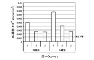
- Example 1 After the maintenance of the vapor phase growth apparatus, when about 1000 silicon epitaxial wafers with a diameter of 300 mm were produced, the chamber was subjected to vapor etching (VE) with HCl gas. Heat treatment was performed in an atmosphere. After the wafer was taken out, a second wafer was put in and subjected to the same heat treatment and taken out. Further, a third wafer was put in and similarly heat-treated and taken out. And each wafer surface contamination was collect
- VE vapor etching
- the measurement results are shown in FIG.
- the left group 101 in FIG. 3 shows the measurement results when the VE and the heat treatment are performed only once
- the middle group 102 shows the measurement results when the VE and the heat treatment are repeated twice
- the right group 103 is the VE.
- the measurement result when heat processing is repeated 4 times is shown.
- the number “1” on the horizontal axis is the first wafer (the first heat-treated wafer)
- “2” is the second wafer (the second heat-treated wafer)
- “3” is 3 This shows the result of the first wafer (the third heat-treated wafer).
- all the groups 101 were below the detection lower limit, but in the group 102, the Mo concentration of the first wafer can be measured.
- the Mo concentration of the first wafer in the group 103 is significantly higher than that in the group 102, and the second wafer is also higher than the detection lower limit. That is, it is shown that Mo concentration can be measured with high sensitivity by repeating VE and heat treatment four times.
- the wafer lifetime (WLT) of each wafer was measured.
- the conditions for VE and heat treatment at this time are the same as those in Example 1 above.
- the measurement results are shown in FIG.
- the number “1” on the horizontal axis in FIG. 4 indicates the result for the first wafer, “2” for the second wafer, and “3” for the third wafer.
- the numerical values above the plot points in FIG. 4 are the values of WLT.
- the WLT is slightly smaller in the order of the third, second, and first sheets, but there is no significant difference, making it difficult to understand the cause of contamination.
- Example 2 The same experiment as in Example 1 was performed. However, this time, within 300 mm diameter silicon epitaxial wafer, the radius is within 85 mm as the inner circumference (see FIG. 5), and the radius from 85 mm to 150 mm (outermost circumference) is 65 mm as the outer circumference (see FIG. 5). 4 times, the inner and outer peripheral parts were compared in terms of Mo concentration in the first to third sheets.
- FIG. 6 shows the measurement results. As shown in FIG. 6, the Mo concentration in the outer peripheral portion is higher than the Mo concentration in the inner peripheral portion in each of the first, second, and third sheets. Usually the outer periphery is more heavily contaminated, but with similar results.
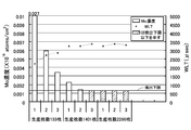
- Example 3 After maintenance of the vapor phase growth apparatus, 133 silicon epitaxial wafers having a diameter of 300 mm were produced, 1401 pieces were produced, and 2266 pieces were produced, respectively. The same VE and heat treatment as in Example 1 were performed four times. , Mo concentration was compared. The measurement results are shown in FIG. The result of WLT is also shown. As shown in FIG. 7, it can be seen that the smaller the number of products produced after maintenance, the higher the Mo concentration in the order of the third, second and first sheets. These are more prominent compared to WLT. However, after the production of 2266 sheets, the contamination due to maintenance has already been removed by exhaust or the like, indicating that all the first to third sheets are below the lower detection limit. Thus, in this invention, it is easy to judge the recovery
- the vapor phase growth apparatus for measuring the amount of contamination is not limited to the single wafer type, and the present invention is used for measuring the amount of contamination of various vapor phase growth apparatuses such as a vertical type (pancake type) and a barrel type (cylinder type). Can be applied.
- the concentration of other metal impurities having a slow diffusion rate such as Sn, W, Ta, Ti, Al, V may be measured.
- the Mo concentration may be measured by a wafer surface analysis method other than ICP-MS, for example, a total reflection X-ray fluorescence (TXRF) analysis method (TXRF: Total Reflection X-Ray Fluorescence).
- TXRF total reflection X-ray fluorescence
- a heat treatment may be applied to a semiconductor wafer other than the silicon wafer.
Landscapes
- Chemical & Material Sciences (AREA)
- Engineering & Computer Science (AREA)
- Life Sciences & Earth Sciences (AREA)
- Health & Medical Sciences (AREA)
- Materials Engineering (AREA)
- Metallurgy (AREA)
- Organic Chemistry (AREA)
- General Physics & Mathematics (AREA)
- Physics & Mathematics (AREA)
- Manufacturing & Machinery (AREA)
- Biochemistry (AREA)
- Immunology (AREA)
- Pathology (AREA)
- General Health & Medical Sciences (AREA)
- Analytical Chemistry (AREA)
- Medicinal Chemistry (AREA)
- Food Science & Technology (AREA)
- Crystallography & Structural Chemistry (AREA)
- Chemical Kinetics & Catalysis (AREA)
- General Chemical & Material Sciences (AREA)
- Power Engineering (AREA)
- Microelectronics & Electronic Packaging (AREA)
- Computer Hardware Design (AREA)
- Mechanical Engineering (AREA)
- Combustion & Propulsion (AREA)
- Condensed Matter Physics & Semiconductors (AREA)
- Testing Or Measuring Of Semiconductors Or The Like (AREA)
- Chemical Vapour Deposition (AREA)
Priority Applications (4)
| Application Number | Priority Date | Filing Date | Title |
|---|---|---|---|
| KR1020157004828A KR101943074B1 (ko) | 2012-10-16 | 2013-09-26 | 기상 성장 장치의 오염량 측정 방법 및 에피택셜 웨이퍼의 제조 방법 |
| CN201380046910.7A CN104620355B (zh) | 2012-10-16 | 2013-09-26 | 气相生长装置的污染量测定方法及外延晶片的制造方法 |
| DE112013005872.3T DE112013005872B4 (de) | 2012-10-16 | 2013-09-26 | Verfahren zum Messen des Verunreinigungsbetrags einer Gasphasenwachstumsvorrichtung und Verfahren zur Herstellung eines Epitaxiewafers |
| US14/426,968 US9437505B2 (en) | 2012-10-16 | 2013-09-26 | Method of measuring contamination amount of vapor phase growth apparatus, and method of manufacturing epitaxial wafer |
Applications Claiming Priority (2)
| Application Number | Priority Date | Filing Date | Title |
|---|---|---|---|
| JP2012229198A JP5884705B2 (ja) | 2012-10-16 | 2012-10-16 | 気相成長装置の汚染量測定方法及びエピタキシャルウェーハの製造方法 |
| JP2012-229198 | 2012-10-16 |
Publications (1)
| Publication Number | Publication Date |
|---|---|
| WO2014061413A1 true WO2014061413A1 (ja) | 2014-04-24 |
Family
ID=50487986
Family Applications (1)
| Application Number | Title | Priority Date | Filing Date |
|---|---|---|---|
| PCT/JP2013/076030 Ceased WO2014061413A1 (ja) | 2012-10-16 | 2013-09-26 | 気相成長装置の汚染量測定方法及びエピタキシャルウェーハの製造方法 |
Country Status (7)
| Country | Link |
|---|---|
| US (1) | US9437505B2 (enExample) |
| JP (1) | JP5884705B2 (enExample) |
| KR (1) | KR101943074B1 (enExample) |
| CN (1) | CN104620355B (enExample) |
| DE (1) | DE112013005872B4 (enExample) |
| TW (1) | TWI520246B (enExample) |
| WO (1) | WO2014061413A1 (enExample) |
Cited By (4)
| Publication number | Priority date | Publication date | Assignee | Title |
|---|---|---|---|---|
| JP2013162026A (ja) * | 2012-02-07 | 2013-08-19 | Shin Etsu Handotai Co Ltd | 気相成長装置の清浄度評価方法及びシリコンエピタキシャルウェーハの製造方法 |
| JP2016063213A (ja) * | 2014-09-18 | 2016-04-25 | 株式会社Sumco | エピタキシャルシリコンウェーハ |
| JP2016076518A (ja) * | 2014-10-02 | 2016-05-12 | 株式会社Sumco | 気相成長装置の汚染管理方法、エピタキシャルシリコンウェーハの製造方法 |
| DE112016003399B4 (de) * | 2015-07-28 | 2025-04-30 | Sk Siltron Co., Ltd. | Verfahren zur Vorbereitung eines Reaktorneustarts zur Herstellung eines epitaktischen Wafers |
Families Citing this family (11)
| Publication number | Priority date | Publication date | Assignee | Title |
|---|---|---|---|---|
| JP6361482B2 (ja) * | 2014-11-26 | 2018-07-25 | 株式会社Sumco | 気相成長装置の汚染管理方法、エピタキシャルシリコンウェーハの製造方法 |
| CN107881491A (zh) * | 2016-09-30 | 2018-04-06 | 非视觉污染分析科学技术有限公司 | 基板污染物分析装置及基板污染物分析方法 |
| CN108426978B (zh) * | 2017-02-14 | 2021-01-01 | 无锡华瑛微电子技术有限公司 | 晶圆局部处理方法 |
| JP6739386B2 (ja) * | 2017-03-28 | 2020-08-12 | 東京エレクトロン株式会社 | 基板処理システム、制御装置、成膜方法及びプログラム |
| JP6711327B2 (ja) | 2017-07-18 | 2020-06-17 | 株式会社Sumco | シリコンウェーハ製造工程の評価方法およびシリコンウェーハの製造方法 |
| KR101988121B1 (ko) * | 2017-08-23 | 2019-06-11 | 에스케이실트론 주식회사 | 실리콘웨이퍼의 금속불순물 검출방법 |
| JP6477854B1 (ja) | 2017-12-22 | 2019-03-06 | 株式会社Sumco | 気相成長装置の汚染管理方法及びエピタキシャルウェーハの製造方法 |
| US10695804B2 (en) * | 2018-01-25 | 2020-06-30 | Applied Materials, Inc. | Equipment cleaning apparatus and method |
| JP7342695B2 (ja) * | 2019-12-26 | 2023-09-12 | 株式会社Sumco | エピタキシャルウェーハ製造システム及び製造方法 |
| CN112683988B (zh) * | 2020-12-28 | 2023-06-02 | 上海新昇半导体科技有限公司 | 一种晶圆中金属杂质的检测方法 |
| CN113782465B (zh) * | 2021-11-11 | 2022-02-18 | 西安奕斯伟材料科技有限公司 | 用于检测晶圆表面金属的方法 |
Citations (3)
| Publication number | Priority date | Publication date | Assignee | Title |
|---|---|---|---|---|
| JPH03101246A (ja) * | 1989-09-14 | 1991-04-26 | Shin Etsu Handotai Co Ltd | 化合物半導体基板表面の重金属汚染評価方法 |
| JPH08148552A (ja) * | 1994-11-17 | 1996-06-07 | Shin Etsu Handotai Co Ltd | 半導体熱処理用治具及びその表面処理方法 |
| JP2006228782A (ja) * | 2005-02-15 | 2006-08-31 | Sumco Corp | 枚葉式エピタキシャルウェーハ製造装置およびその保守方法 |
Family Cites Families (7)
| Publication number | Priority date | Publication date | Assignee | Title |
|---|---|---|---|---|
| US6749687B1 (en) * | 1998-01-09 | 2004-06-15 | Asm America, Inc. | In situ growth of oxide and silicon layers |
| EP1044291B1 (en) | 1998-01-09 | 2003-04-02 | ASM America, Inc. | In situ growth of oxide and silicon layers |
| JP4393071B2 (ja) * | 2002-07-12 | 2010-01-06 | 東京エレクトロン株式会社 | 成膜方法 |
| US20050136657A1 (en) | 2002-07-12 | 2005-06-23 | Tokyo Electron Limited | Film-formation method for semiconductor process |
| JP5407212B2 (ja) * | 2008-08-06 | 2014-02-05 | 株式会社Sumco | 熱処理炉評価方法および半導体ウェーハの製造方法 |
| JP5024224B2 (ja) | 2008-08-06 | 2012-09-12 | 信越半導体株式会社 | シリコン基板の評価方法、汚染検出方法及びエピタキシャル基板の製造方法 |
| JP5413342B2 (ja) * | 2010-09-27 | 2014-02-12 | 株式会社Sumco | シリコンウェーハ表層部のエッチング方法およびシリコンウェーハの金属汚染分析方法 |
-
2012
- 2012-10-16 JP JP2012229198A patent/JP5884705B2/ja active Active
-
2013
- 2013-09-26 KR KR1020157004828A patent/KR101943074B1/ko active Active
- 2013-09-26 CN CN201380046910.7A patent/CN104620355B/zh active Active
- 2013-09-26 WO PCT/JP2013/076030 patent/WO2014061413A1/ja not_active Ceased
- 2013-09-26 US US14/426,968 patent/US9437505B2/en active Active
- 2013-09-26 DE DE112013005872.3T patent/DE112013005872B4/de active Active
- 2013-10-04 TW TW102135981A patent/TWI520246B/zh active
Patent Citations (3)
| Publication number | Priority date | Publication date | Assignee | Title |
|---|---|---|---|---|
| JPH03101246A (ja) * | 1989-09-14 | 1991-04-26 | Shin Etsu Handotai Co Ltd | 化合物半導体基板表面の重金属汚染評価方法 |
| JPH08148552A (ja) * | 1994-11-17 | 1996-06-07 | Shin Etsu Handotai Co Ltd | 半導体熱処理用治具及びその表面処理方法 |
| JP2006228782A (ja) * | 2005-02-15 | 2006-08-31 | Sumco Corp | 枚葉式エピタキシャルウェーハ製造装置およびその保守方法 |
Cited By (7)
| Publication number | Priority date | Publication date | Assignee | Title |
|---|---|---|---|---|
| JP2013162026A (ja) * | 2012-02-07 | 2013-08-19 | Shin Etsu Handotai Co Ltd | 気相成長装置の清浄度評価方法及びシリコンエピタキシャルウェーハの製造方法 |
| JP2016063213A (ja) * | 2014-09-18 | 2016-04-25 | 株式会社Sumco | エピタキシャルシリコンウェーハ |
| TWI584348B (zh) * | 2014-09-18 | 2017-05-21 | Sumco股份有限公司 | 磊晶矽晶圓的製造方法、氣相成長裝置及磊晶矽晶圓 |
| US9670581B2 (en) | 2014-09-18 | 2017-06-06 | Sumco Corporation | Production method of epitaxial silicon wafer and vapor deposition apparatus |
| JP2016076518A (ja) * | 2014-10-02 | 2016-05-12 | 株式会社Sumco | 気相成長装置の汚染管理方法、エピタキシャルシリコンウェーハの製造方法 |
| US10379094B2 (en) * | 2014-10-02 | 2019-08-13 | Sumco Corporation | Contamination control method of vapor deposition apparatus and method of producing epitaxial silicon wafer |
| DE112016003399B4 (de) * | 2015-07-28 | 2025-04-30 | Sk Siltron Co., Ltd. | Verfahren zur Vorbereitung eines Reaktorneustarts zur Herstellung eines epitaktischen Wafers |
Also Published As
| Publication number | Publication date |
|---|---|
| CN104620355A (zh) | 2015-05-13 |
| KR101943074B1 (ko) | 2019-01-28 |
| US9437505B2 (en) | 2016-09-06 |
| DE112013005872T5 (de) | 2015-08-20 |
| KR20150066515A (ko) | 2015-06-16 |
| CN104620355B (zh) | 2017-03-15 |
| US20150243566A1 (en) | 2015-08-27 |
| TWI520246B (zh) | 2016-02-01 |
| TW201421595A (zh) | 2014-06-01 |
| JP2014082324A (ja) | 2014-05-08 |
| JP5884705B2 (ja) | 2016-03-15 |
| DE112013005872B4 (de) | 2022-06-30 |
Similar Documents
| Publication | Publication Date | Title |
|---|---|---|
| JP5884705B2 (ja) | 気相成長装置の汚染量測定方法及びエピタキシャルウェーハの製造方法 | |
| US10176987B2 (en) | SiC epitaxial wafer and method for manufacturing the same | |
| JP5839343B2 (ja) | 気相成長装置の汚染検出方法及びエピタキシャルウェーハの製造方法 | |
| JP5880974B2 (ja) | エピタキシャル成長装置の汚染検出方法及びエピタキシャルウェーハの製造方法 | |
| TWI713946B (zh) | 氣相成長裝置的汙染管理方法及磊晶晶圓的製造方法 | |
| JP6098997B2 (ja) | エピタキシャル成長装置の汚染評価方法及びエピタキシャルウェーハの製造方法 | |
| JP5228857B2 (ja) | シリコンエピタキシャルウェーハの製造方法 | |
| JP6327094B2 (ja) | 気相成長装置の汚染管理方法、エピタキシャルシリコンウェーハの製造方法 | |
| JP5936007B2 (ja) | 気相エピタキシャル成長装置の汚染評価方法及びエピタキシャルウェーハの製造方法 | |
| JP5794212B2 (ja) | 気相成長装置の汚染評価方法及びシリコンエピタキシャルウェーハの製造方法 | |
| JP6090183B2 (ja) | 気相成長装置の清掃又は点検方法及びエピタキシャルウェーハの製造方法 | |
| JP6489198B1 (ja) | エピタキシャルウェーハの汚染評価方法および該方法を用いたエピタキシャルウェーハの製造方法 | |
| JP6361482B2 (ja) | 気相成長装置の汚染管理方法、エピタキシャルシリコンウェーハの製造方法 | |
| JP6024595B2 (ja) | ガスフィルターのライフ管理方法 | |
| JP2015035460A (ja) | エピタキシャルウェーハの製造方法 | |
| JP6475609B2 (ja) | エピタキシャルウェーハの製造方法 | |
| WO2007032180A1 (ja) | エピタキシャルウエーハの製造方法及びそれにより製造されたエピタキシャルウエーハ | |
| JP2013149753A (ja) | 気相成長装置の清浄度評価方法及びシリコンエピタキシャルウェーハの製造方法 | |
| JP2018157138A (ja) | エピタキシャルウェーハの製造方法 | |
| JP5454298B2 (ja) | 半導体基板の製造方法 |
Legal Events
| Date | Code | Title | Description |
|---|---|---|---|
| 121 | Ep: the epo has been informed by wipo that ep was designated in this application |
Ref document number: 13846788 Country of ref document: EP Kind code of ref document: A1 |
|
| ENP | Entry into the national phase |
Ref document number: 20157004828 Country of ref document: KR Kind code of ref document: A |
|
| WWE | Wipo information: entry into national phase |
Ref document number: 14426968 Country of ref document: US |
|
| WWE | Wipo information: entry into national phase |
Ref document number: 1120130058723 Country of ref document: DE Ref document number: 112013005872 Country of ref document: DE |
|
| 122 | Ep: pct application non-entry in european phase |
Ref document number: 13846788 Country of ref document: EP Kind code of ref document: A1 |