WO2014010342A1 - シールドフィルム、及び、シールドプリント配線板 - Google Patents
シールドフィルム、及び、シールドプリント配線板 Download PDFInfo
- Publication number
- WO2014010342A1 WO2014010342A1 PCT/JP2013/065616 JP2013065616W WO2014010342A1 WO 2014010342 A1 WO2014010342 A1 WO 2014010342A1 JP 2013065616 W JP2013065616 W JP 2013065616W WO 2014010342 A1 WO2014010342 A1 WO 2014010342A1
- Authority
- WO
- WIPO (PCT)
- Prior art keywords
- shield
- layer
- shield film
- wiring board
- printed wiring
- Prior art date
- Legal status (The legal status is an assumption and is not a legal conclusion. Google has not performed a legal analysis and makes no representation as to the accuracy of the status listed.)
- Ceased
Links
Images





Classifications
-
- B—PERFORMING OPERATIONS; TRANSPORTING
- B32—LAYERED PRODUCTS
- B32B—LAYERED PRODUCTS, i.e. PRODUCTS BUILT-UP OF STRATA OF FLAT OR NON-FLAT, e.g. CELLULAR OR HONEYCOMB, FORM
- B32B7/00—Layered products characterised by the relation between layers; Layered products characterised by the relative orientation of features between layers, or by the relative values of a measurable parameter between layers, i.e. products comprising layers having different physical, chemical or physicochemical properties; Layered products characterised by the interconnection of layers
- B32B7/04—Interconnection of layers
- B32B7/12—Interconnection of layers using interposed adhesives or interposed materials with bonding properties
-
- H—ELECTRICITY
- H05—ELECTRIC TECHNIQUES NOT OTHERWISE PROVIDED FOR
- H05K—PRINTED CIRCUITS; CASINGS OR CONSTRUCTIONAL DETAILS OF ELECTRIC APPARATUS; MANUFACTURE OF ASSEMBLAGES OF ELECTRICAL COMPONENTS
- H05K9/00—Screening of apparatus or components against electric or magnetic fields
- H05K9/0073—Shielding materials
- H05K9/0081—Electromagnetic shielding materials, e.g. EMI, RFI shielding
- H05K9/0088—Electromagnetic shielding materials, e.g. EMI, RFI shielding comprising a plurality of shielding layers; combining different shielding material structure
-
- H—ELECTRICITY
- H05—ELECTRIC TECHNIQUES NOT OTHERWISE PROVIDED FOR
- H05K—PRINTED CIRCUITS; CASINGS OR CONSTRUCTIONAL DETAILS OF ELECTRIC APPARATUS; MANUFACTURE OF ASSEMBLAGES OF ELECTRICAL COMPONENTS
- H05K9/00—Screening of apparatus or components against electric or magnetic fields
- H05K9/0073—Shielding materials
- H05K9/0081—Electromagnetic shielding materials, e.g. EMI, RFI shielding
- H05K9/0084—Electromagnetic shielding materials, e.g. EMI, RFI shielding comprising a single continuous metallic layer on an electrically insulating supporting structure, e.g. metal foil, film, plating coating, electro-deposition, vapour-deposition
-
- B—PERFORMING OPERATIONS; TRANSPORTING
- B32—LAYERED PRODUCTS
- B32B—LAYERED PRODUCTS, i.e. PRODUCTS BUILT-UP OF STRATA OF FLAT OR NON-FLAT, e.g. CELLULAR OR HONEYCOMB, FORM
- B32B15/00—Layered products comprising a layer of metal
-
- B—PERFORMING OPERATIONS; TRANSPORTING
- B32—LAYERED PRODUCTS
- B32B—LAYERED PRODUCTS, i.e. PRODUCTS BUILT-UP OF STRATA OF FLAT OR NON-FLAT, e.g. CELLULAR OR HONEYCOMB, FORM
- B32B15/00—Layered products comprising a layer of metal
- B32B15/04—Layered products comprising a layer of metal comprising metal as the main or only constituent of a layer, which is next to another layer of the same or of a different material
-
- B—PERFORMING OPERATIONS; TRANSPORTING
- B32—LAYERED PRODUCTS
- B32B—LAYERED PRODUCTS, i.e. PRODUCTS BUILT-UP OF STRATA OF FLAT OR NON-FLAT, e.g. CELLULAR OR HONEYCOMB, FORM
- B32B15/00—Layered products comprising a layer of metal
- B32B15/20—Layered products comprising a layer of metal comprising aluminium or copper
-
- H—ELECTRICITY
- H05—ELECTRIC TECHNIQUES NOT OTHERWISE PROVIDED FOR
- H05K—PRINTED CIRCUITS; CASINGS OR CONSTRUCTIONAL DETAILS OF ELECTRIC APPARATUS; MANUFACTURE OF ASSEMBLAGES OF ELECTRICAL COMPONENTS
- H05K1/00—Printed circuits
- H05K1/02—Details
- H05K1/0213—Electrical arrangements not otherwise provided for
- H05K1/0215—Grounding of printed circuits by connection to external grounding means
-
- H—ELECTRICITY
- H05—ELECTRIC TECHNIQUES NOT OTHERWISE PROVIDED FOR
- H05K—PRINTED CIRCUITS; CASINGS OR CONSTRUCTIONAL DETAILS OF ELECTRIC APPARATUS; MANUFACTURE OF ASSEMBLAGES OF ELECTRICAL COMPONENTS
- H05K1/00—Printed circuits
- H05K1/02—Details
- H05K1/0213—Electrical arrangements not otherwise provided for
- H05K1/0216—Reduction of cross-talk, noise or electromagnetic interference
-
- H—ELECTRICITY
- H05—ELECTRIC TECHNIQUES NOT OTHERWISE PROVIDED FOR
- H05K—PRINTED CIRCUITS; CASINGS OR CONSTRUCTIONAL DETAILS OF ELECTRIC APPARATUS; MANUFACTURE OF ASSEMBLAGES OF ELECTRICAL COMPONENTS
- H05K1/00—Printed circuits
- H05K1/02—Details
- H05K1/0213—Electrical arrangements not otherwise provided for
- H05K1/0216—Reduction of cross-talk, noise or electromagnetic interference
- H05K1/0218—Reduction of cross-talk, noise or electromagnetic interference by printed shielding conductors, ground planes or power plane
-
- H—ELECTRICITY
- H05—ELECTRIC TECHNIQUES NOT OTHERWISE PROVIDED FOR
- H05K—PRINTED CIRCUITS; CASINGS OR CONSTRUCTIONAL DETAILS OF ELECTRIC APPARATUS; MANUFACTURE OF ASSEMBLAGES OF ELECTRICAL COMPONENTS
- H05K1/00—Printed circuits
- H05K1/02—Details
- H05K1/0296—Conductive pattern lay-out details not covered by sub groups H05K1/02 - H05K1/0295
-
- B—PERFORMING OPERATIONS; TRANSPORTING
- B32—LAYERED PRODUCTS
- B32B—LAYERED PRODUCTS, i.e. PRODUCTS BUILT-UP OF STRATA OF FLAT OR NON-FLAT, e.g. CELLULAR OR HONEYCOMB, FORM
- B32B2307/00—Properties of the layers or laminate
- B32B2307/20—Properties of the layers or laminate having particular electrical or magnetic properties, e.g. piezoelectric
- B32B2307/202—Conductive
-
- B—PERFORMING OPERATIONS; TRANSPORTING
- B32—LAYERED PRODUCTS
- B32B—LAYERED PRODUCTS, i.e. PRODUCTS BUILT-UP OF STRATA OF FLAT OR NON-FLAT, e.g. CELLULAR OR HONEYCOMB, FORM
- B32B2307/00—Properties of the layers or laminate
- B32B2307/20—Properties of the layers or laminate having particular electrical or magnetic properties, e.g. piezoelectric
- B32B2307/206—Insulating
-
- B—PERFORMING OPERATIONS; TRANSPORTING
- B32—LAYERED PRODUCTS
- B32B—LAYERED PRODUCTS, i.e. PRODUCTS BUILT-UP OF STRATA OF FLAT OR NON-FLAT, e.g. CELLULAR OR HONEYCOMB, FORM
- B32B2457/00—Electrical equipment
-
- H—ELECTRICITY
- H05—ELECTRIC TECHNIQUES NOT OTHERWISE PROVIDED FOR
- H05K—PRINTED CIRCUITS; CASINGS OR CONSTRUCTIONAL DETAILS OF ELECTRIC APPARATUS; MANUFACTURE OF ASSEMBLAGES OF ELECTRICAL COMPONENTS
- H05K2201/00—Indexing scheme relating to printed circuits covered by H05K1/00
- H05K2201/01—Dielectrics
- H05K2201/0137—Materials
- H05K2201/0154—Polyimide
-
- H—ELECTRICITY
- H05—ELECTRIC TECHNIQUES NOT OTHERWISE PROVIDED FOR
- H05K—PRINTED CIRCUITS; CASINGS OR CONSTRUCTIONAL DETAILS OF ELECTRIC APPARATUS; MANUFACTURE OF ASSEMBLAGES OF ELECTRICAL COMPONENTS
- H05K2201/00—Indexing scheme relating to printed circuits covered by H05K1/00
- H05K2201/03—Conductive materials
- H05K2201/0332—Structure of the conductor
- H05K2201/0335—Layered conductors or foils
- H05K2201/0338—Layered conductor, e.g. layered metal substrate, layered finish layer or layered thin film adhesion layer
-
- H—ELECTRICITY
- H05—ELECTRIC TECHNIQUES NOT OTHERWISE PROVIDED FOR
- H05K—PRINTED CIRCUITS; CASINGS OR CONSTRUCTIONAL DETAILS OF ELECTRIC APPARATUS; MANUFACTURE OF ASSEMBLAGES OF ELECTRICAL COMPONENTS
- H05K2201/00—Indexing scheme relating to printed circuits covered by H05K1/00
- H05K2201/03—Conductive materials
- H05K2201/0332—Structure of the conductor
- H05K2201/0335—Layered conductors or foils
- H05K2201/0347—Overplating, e.g. for reinforcing conductors or bumps; Plating over filled vias
-
- H—ELECTRICITY
- H05—ELECTRIC TECHNIQUES NOT OTHERWISE PROVIDED FOR
- H05K—PRINTED CIRCUITS; CASINGS OR CONSTRUCTIONAL DETAILS OF ELECTRIC APPARATUS; MANUFACTURE OF ASSEMBLAGES OF ELECTRICAL COMPONENTS
- H05K2201/00—Indexing scheme relating to printed circuits covered by H05K1/00
- H05K2201/03—Conductive materials
- H05K2201/0332—Structure of the conductor
- H05K2201/0335—Layered conductors or foils
- H05K2201/0355—Metal foils
-
- H—ELECTRICITY
- H05—ELECTRIC TECHNIQUES NOT OTHERWISE PROVIDED FOR
- H05K—PRINTED CIRCUITS; CASINGS OR CONSTRUCTIONAL DETAILS OF ELECTRIC APPARATUS; MANUFACTURE OF ASSEMBLAGES OF ELECTRICAL COMPONENTS
- H05K2201/00—Indexing scheme relating to printed circuits covered by H05K1/00
- H05K2201/07—Electric details
- H05K2201/0707—Shielding
-
- H—ELECTRICITY
- H05—ELECTRIC TECHNIQUES NOT OTHERWISE PROVIDED FOR
- H05K—PRINTED CIRCUITS; CASINGS OR CONSTRUCTIONAL DETAILS OF ELECTRIC APPARATUS; MANUFACTURE OF ASSEMBLAGES OF ELECTRICAL COMPONENTS
- H05K2201/00—Indexing scheme relating to printed circuits covered by H05K1/00
- H05K2201/07—Electric details
- H05K2201/0707—Shielding
- H05K2201/0715—Shielding provided by an outer layer of PCB
-
- H—ELECTRICITY
- H05—ELECTRIC TECHNIQUES NOT OTHERWISE PROVIDED FOR
- H05K—PRINTED CIRCUITS; CASINGS OR CONSTRUCTIONAL DETAILS OF ELECTRIC APPARATUS; MANUFACTURE OF ASSEMBLAGES OF ELECTRICAL COMPONENTS
- H05K2203/00—Indexing scheme relating to apparatus or processes for manufacturing printed circuits covered by H05K3/00
- H05K2203/07—Treatments involving liquids, e.g. plating, rinsing
- H05K2203/0703—Plating
- H05K2203/072—Electroless plating, e.g. finish plating or initial plating
-
- H—ELECTRICITY
- H05—ELECTRIC TECHNIQUES NOT OTHERWISE PROVIDED FOR
- H05K—PRINTED CIRCUITS; CASINGS OR CONSTRUCTIONAL DETAILS OF ELECTRIC APPARATUS; MANUFACTURE OF ASSEMBLAGES OF ELECTRICAL COMPONENTS
- H05K2203/00—Indexing scheme relating to apparatus or processes for manufacturing printed circuits covered by H05K3/00
- H05K2203/07—Treatments involving liquids, e.g. plating, rinsing
- H05K2203/0703—Plating
- H05K2203/0723—Electroplating, e.g. finish plating
Definitions
- the present invention relates to a shield film and a shield printed wiring board used for portable devices, personal computers, earphone jacks, camera modules, and the like.
- shield films are mainly used for printed wiring boards for the purpose of suppressing noise and shielding electromagnetic waves to the outside.
- the shield film in a shielded flexible printed wiring board in which a shield film is coated on at least one surface of a base film in which a printed circuit and an insulating film are sequentially provided on a base film, the shield film is a cover film.
- a shielded flexible printed wiring board having a ground member which is connected and formed so that the other part is exposed and can be connected to a ground part in the vicinity thereof.
- a shield film can effectively exhibit an electromagnetic wave shielding function by laminating a ground member on a shield layer of a printed wiring board and connecting the ground from the outside.
- Patent Document 1 also describes a method of embedding a ground member in the shield film. However, it is necessary to protrude the ground member from the side of the shield film and expose the ground member. There was a problem of limiting the shape. Moreover, when a shield printed wiring board is reduced in size, there exists a problem that attachment of a ground member becomes difficult. Furthermore, since it is necessary to laminate the ground member on the shield layer, there is a problem that the thinning is limited.
- the present invention provides a shield film and a shield printed wiring board that have an electromagnetic wave shielding effect and can be grounded from an arbitrary place from the outside, and can be reduced in size and thickness. Objective.
- the shield film of the present invention is a shield film provided on a printed wiring board having a base member on which a signal wiring pattern is formed and an insulating film that covers the signal wiring pattern and is provided on the entire surface of the base member. And it has the conductive adhesive layer laminated
- the metal layer is laminated on the entire surface of the conductive adhesive layer covering the printed wiring board, and can be connected to the external ground at any location of the metal layer. .
- the metal layer can be connected to the external ground without providing a general ground member on the shield film, and the metal layer can effectively exhibit the electromagnetic wave shielding function.
- the thickness can be reduced, and the circuit pattern on the printed wiring board is not limited by the ground member, so that the size can be reduced.
- the metal layer may be a metal foil mainly composed of copper. According to said structure, while being able to obtain favorable workability and electroconductivity, an inexpensive shield film can be obtained.
- the metal layer may be processed to a thickness of 2 ⁇ m to 12 ⁇ m. According to said structure, a favorable shield characteristic can be acquired.
- the shield film of this invention WHEREIN:
- the said metal layer may be rust-proofed on the surface. According to said structure, deterioration of the surface of a metal layer can be reduced with electroconductivity.
- the shield film of the present invention may further include a plating layer laminated on the entire surface of the metal layer. According to said structure, deterioration of the metal layer surface by use environment can be reduced, and electrical characteristics, such as resistance value, can be stabilized over a long period of time. Thereby, a stable electromagnetic wave shielding effect can be obtained.
- the plating layer may be a layer in which at least one layer is formed of soft nickel. According to said structure, a favorable deformation characteristic can be acquired.
- the plating layer may be a layer in which at least one layer is formed by soft gold plating. According to said structure, a favorable deformation characteristic can be acquired.
- At least the surface of the plating layer may be black.
- a general shield film attached to a printed wiring board is black. According to the said structure, even in the case of this invention which does not affix a general shield film, it can conform to the conventional appearance.
- the shield film of the present invention may have a minimum width of 10 mm or less. According to the said structure, even if the minimum width
- a ground wiring pattern is formed on the base member, and the insulating film exposes at least a part of the ground wiring pattern.
- the conductive adhesive layer may be connected to an exposed portion of the ground wiring pattern.
- the shield printed wiring board of the present invention may be a shield printed wiring board including the printed wiring board and the shield film provided on the printed wiring board.
- A) is a figure which shows an electric field wave shield effect evaluation apparatus.
- B) is a figure which shows a magnetic field wave shield effect evaluation apparatus.
- A) It is a figure which shows the measurement result of the electric field wave shield performance by KEC method.
- (B) It is a figure which shows the measurement result of the magnetic wave shield performance by KEC method.
- A It is a figure which shows the measurement result of the output waveform characteristic in case a bit rate is 1.0 Gbps.
- B It is a figure which shows the measurement result of the output waveform characteristic in case a bit rate is 3.0 Gbps.
- the shield film 1 is provided on the entire surface of the base film 5 covering the signal circuit 6a and the base film 5 (base member) on which the signal circuit 6a (signal wiring pattern) is formed.
- the flexible printed wiring board 8 printed wiring board having the insulating film 7 is provided.
- the shield film 1 has a conductive adhesive layer 15 laminated on the entire surface of the insulating film 7 and a metal layer 11 laminated on the entire surface of the conductive adhesive layer 15.
- the shape of the surface direction of the shield film 1 is not specifically limited.
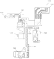
- the example of the top view of the shield printed wiring board provided with the shield film is shown in FIG.
- the shield printed wiring board 110 may be formed in a complicated shape as shown in FIG.
- the shield printed wiring board 110 includes a plurality of block portions 120 (block portions 121, 122, 123, 124, and 125) and connection portions 130 (connection portions 131, 132, 133, and 134) that connect these blocks.
- a shield film is attached to a place where an electromagnetic wave shield is required.
- the shield printed wiring board 110 having the above-described configuration is configured such that each block portion 120 is connected by a connection portion 130 that is formed to be longer than the block portion 120.
- Each block unit 120 is provided with various electronic components connected to the wiring pattern, and the electronic components are electrically connected by the wiring pattern formed in the connection unit 130.
- the shield printed wiring board 110 is three-dimensionally housed in a housing or the like with each connection portion 130 bent, and a screw or the like is screwed through a through hole formed in each block portion 130. Is fixed to the housing or the like.
- the shield printed wiring board 110 has an area formed with a narrow width like the connection portion 130.
- the shield film needs to be grounded even in such a thinly formed portion.
- the minimum width of the connecting portion 130 is formed to be 10 mm or less.
- the metal layer is laminated
- FIG. 1 the shape of a shield printed wiring board (shield film) is not limited to the shape where the above block parts are connected by a connection part.
- it may be a polygon, a circle, an ellipse, a shape in which irregularities are added to these, a shape in which a through hole or a protrusion for forming a through hole is added, and the like.
- the minimum width may be 10 mm or less.
- the metal layer 11 of this embodiment is formed of a metal foil containing copper as a main component. That is, the metal layer 11 has the plating layer 12 on the outermost surface.
- the metal layer is not limited to this configuration.
- the metal layer may be two or more layers.
- the metal layer 11 is preferably formed by rolling.
- a shield film can have favorable shape retainability. Therefore, the workability at the time of assembling the flexible substrate with the shield film attached can be improved. For example, when a flexible printed wiring board provided with a shield film is bent and assembled to a portable device or the like, the flexible printed wiring board maintains its bent state due to its good shape retention, There is no need for the operator to maintain the bent state, the load of the assembling work of the portable device or the like can be reduced, and good workability is obtained. Furthermore, when the metal layer 11 is formed by rolling, the layer thickness is preferably adjusted by etching.
- the metal material forming the metal layer 11 is preferably composed mainly of copper. Thereby, while being able to obtain favorable electroconductivity, a shield film can be manufactured cheaply.
- the metal layer 11 is not limited to copper as a main component, and is any one of nickel, copper, silver, tin, gold, palladium, aluminum, chromium, titanium, and zinc, or two or more of these.
- the metal layer 11 is not limited to being a metal foil formed by rolling, but is formed by a special electrolytic plating method so that the crystal has a structure in which crystals are spread in the plane direction, similar to the metal foil. It may be a layer. Thereby, like shape rolling, favorable shape retainability can be obtained.
- the lower limit of the thickness of the metal layer 11 is preferably 2 ⁇ m, and more preferably 6 ⁇ m. Moreover, 18 micrometers is preferable and the upper limit of the thickness of the metal layer 11 has more preferable 12 micrometers.
- the surface is rust-proofed.
- rust preventive water-soluble ones are suitable, and it is preferable that benzotriazole or imidazole compound is contained as the main component.
- a Toughace (trademark) series manufactured by Shikoku Kasei Kogyo Co., Ltd. can be used, and a 0.2 to 0.3 ⁇ m film can be formed on the copper surface.
- the plating layer 12 is laminated on the entire surface of the metal layer 11.
- the plating layer 12 is formed by an electrolytic plating method, an electroless plating method, or the like. By forming the plating layer 12 on the outermost surface, deterioration of the surface of the metal layer 11 can be reduced while maintaining conductivity.
- the metal material of the plating layer 12 include gold, nickel, copper, silver, tin, palladium, aluminum, chromium, titanium, zinc, and an alloy including any one or more of these materials. .
- the lower limit of the thickness of the plating layer 12 is preferably 0.1 ⁇ m, and more preferably 0.3 ⁇ m.
- the upper limit of the thickness of the plating layer 12 is preferably 5 ⁇ m, and more preferably 3 ⁇ m.
- nickel When nickel is used for the metal material of the plating layer 12, it is preferably soft nickel.
- soft nickel shows what was formed using the sulfamic acid bath as a nickel plating bath.
- Soft nickel has a lower electrodeposition stress than that formed by using a watt bath and can reduce internal stress, so that it is possible to obtain good deformation characteristics such as resistance to bending.
- gold when gold is used for the metal material of the plating layer 12, it is preferably a soft gold plating having a purity of 99.99% or more. Thereby, a favorable deformation characteristic can be obtained.
- at least the surface of the plating layer is formed in black in accordance with black which is a color of a general shield film.
- the plating layer 12 may be formed into black plating by nickel tin alloy plating or the like, or a black conductive adhesive layer may be formed on the plating surface.
- the plated layer 12 is a layer formed by performing a nickel plating process on the metal layer 11 to form a soft nickel layer, and then performing a gold plating process to form a soft gold plated layer. That is, the plating layer 12 is formed of two layers, but is not limited to this.
- the plating layer may be a single layer or three or more layers. That is, the plating process may be performed once or more.
- the conductive adhesive layer 15 is preferably an anisotropic conductive adhesive layer having anisotropic conductivity in which an electrically conductive state is ensured only in the thickness direction from the viewpoint of transmission characteristics and cost, but is not limited thereto.
- the conductive adhesive layer 15 is an isotropic conductive adhesive layer having isotropic conductivity in which an electrically conductive state is ensured in all three directions including a thickness direction, a width direction, and a longitudinal direction. May be.
- the conductive adhesive layer 15 is formed by adding a flame retardant or a conductive filler to an adhesive.
- the lower limit of the thickness of the conductive adhesive layer 15 is preferably 2 ⁇ m, and more preferably 3 ⁇ m. Further, the upper limit of the thickness of the conductive adhesive layer 15 is preferably 15 ⁇ m, and more preferably 9 ⁇ m.
- the adhesive contained in the conductive adhesive layer 15 includes, as an adhesive resin, a thermoplastic resin such as polystyrene, vinyl acetate, polyester, polyethylene, polypropylene, polyamide, rubber, or acrylic, or phenol. It is composed of thermosetting resins such as epoxy, epoxy, urethane, melamine, and alkyd.
- the adhesive may be a single substance or a mixture of the above resins.
- the adhesive may further contain a tackifier. Examples of the tackifier include tackifiers such as fatty acid hydrocarbon resins, C5 / C9 mixed resins, rosin, rosin derivatives, terpene resins, aromatic hydrocarbon resins, and thermally reactive resins.
- the conductive filler added to the conductive adhesive layer 15 is partially or entirely formed of a metal material.
- conductive fillers include copper powder, silver powder, nickel powder, silver coated copper powder (Ag coated Cu powder), gold coated copper powder, silver coated nickel powder (Ag coated Ni powder), and gold coated nickel powder.
- the metal powder can be produced by an atomizing method, a carbonyl method, or the like.
- particles obtained by coating a metal powder with a resin and particles obtained by coating a resin with a metal powder can also be used.
- one or more kinds of conductive fillers may be mixed and added to the conductive adhesive layer 15.
- the conductive filler is preferably Ag-coated Cu powder or Ag-coated Ni powder. This is because conductive particles having stable conductivity can be obtained from an inexpensive material.
- the conductive filler is added in the range of 3 wt% to 39 wt% in the case of the anisotropic conductive adhesive layer with respect to the total amount of the conductive adhesive layer 15, and 39 wt% in the case of the isotropic conductive adhesive layer. It is added at a rate exceeding%.
- the average particle size of the conductive filler is preferably in the range of 2 ⁇ m to 20 ⁇ m, but an optimal value may be selected depending on the thickness of the conductive adhesive layer 15.
- the shape of the metal filler may be spherical, needle-like, fiber-like, flake-like, or dendritic.
- shield printed wiring board 10 (Configuration of shield printed wiring board 10)
- FPC flexible printed wiring board
- this embodiment demonstrates the case where a shield film is affixed on FPC, it is not limited to this.
- it can be used for COF (chip on flex), RF (rigid flex printed board), multilayer flexible substrate, rigid substrate and the like.
- the shield printed wiring board 10 is formed by laminating the shield film 1 and the flexible printed wiring board 8 described above.
- the flexible printed wiring board 8 is formed by sequentially laminating a base film 5, a printed circuit 6, and an insulating film 7.
- the surface of the printed circuit 6 includes a signal circuit 6a and a ground circuit 6b, and is covered with an insulating film 7 except for at least a part of the ground circuit 6b (insulation removing portion 6c).
- the insulating film 7 has the insulation removal part 7a in which a part of the conductive adhesive layer 15 of the shield film 1 flows into the inside. Thereby, the ground circuit 6b and the metal layer 11 are electrically connected.
- the signal circuit 6a and the ground circuit 6b are formed with a wiring pattern by etching the conductive material.
- the ground circuit 6b refers to a pattern that maintains the ground potential. That is, the base film 5 is formed with a ground circuit 6b which is a ground wiring pattern.
- the wiring pattern formed on the base film 5 may be configured to include only the signal circuit 6a.
- the ground circuit 6 b may not be included in the wiring pattern formed on the base film 5.
- the insulating removal portion 6 c is not formed on the insulating film 7.
- the shield printed wiring board 10 includes the base member (base film 5) on which the signal wiring pattern (signal circuit 6a) is formed, and the insulating film 7 that covers the signal wiring pattern. And the shield film 1 is affixed on the insulating film 7 by adhesion of the conductive adhesive layer 15. More specifically, the shield printed wiring board 10 includes a base member (base film 5) on which a signal wiring pattern (signal circuit 6a) and a ground wiring pattern (ground circuit 6b) are formed, and a signal wiring. And an insulating film 7 provided on the base member so as to cover the pattern and expose at least a part of the ground wiring pattern. And the shield film 1 is affixed on the insulating film 7 by adhesion of the conductive adhesive layer 15.
- the base film 5 and the printed circuit 6 may be bonded together by an adhesive, or may be bonded in the same manner as a so-called adhesiveless copper-clad laminate that does not use an adhesive.
- the insulating film 7 may be formed by bonding a flexible insulating film using an adhesive, or by a series of techniques such as application of a photosensitive insulating resin, drying, exposure, development, and heat treatment. . When the insulating film 7 is attached using an adhesive, the insulating removal portion 7a is also formed at the location of the ground circuit 6b of the adhesive.
- the flexible printed wiring board 8 has a single-sided FPC having a printed circuit only on one side of the base film, a double-sided FPC having a printed circuit on both sides of the base film, and a plurality of such FPCs are laminated.
- the base film 5 and the insulating film 7 are both made of engineering plastic. Examples thereof include resins such as polyethylene terephthalate, polypropylene, crosslinked polyethylene, polyester, polybenzimidazole, polyimide, polyimide amide, polyether imide, and polyphenylene sulfide (PPS).
- resins such as polyethylene terephthalate, polypropylene, crosslinked polyethylene, polyester, polybenzimidazole, polyimide, polyimide amide, polyether imide, and polyphenylene sulfide (PPS).
- PPS polyphenylene sulfide
- An inexpensive polyester film is preferable when heat resistance is not required, and a polyphenylene sulfide film is preferable when flame resistance is required, and a polyimide film is preferable when heat resistance is required.
- 10 micrometers is preferable and the minimum of the thickness of the base film 5 has more preferable 20 micrometers.
- the upper limit of the thickness of the base film 5 is preferably 60 ⁇ m, and more preferably 40 ⁇ m.
- the lower limit of the thickness of the insulating film 7 is preferably 10 ⁇ m, and more preferably 20 ⁇ m.
- the upper limit of the thickness of the insulating film 7 is preferably 60 ⁇ m, and more preferably 40 ⁇ m.
- the conductive adhesive layer 15 and the metal layer 11 are laminated on the entire surface of the flexible printed wiring board 8 from which a part of the ground circuit 6b is exposed.
- the exposed ground circuit 6b is electrically connected to the metal layer 11 laminated on the entire surface of the conductive adhesive layer 15, so that it can be connected to the external ground at any location of the metal layer 11. become.
- the metal layer 11 is provided on the entire surface of the flexible printed wiring board 8, the shield function can be exhibited in any region of the shield film 1.
- the shield film 1 can be configured without being divided into two types for both the signal circuit 6a region and the ground circuit 6b region, the signal circuit 6a and the ground on the flexible printed wiring board 8 can be formed.
- the arrangement mode of the circuit 6b is not limited and can be reduced in size and cost.
- Method for producing shield film 1 An example of the manufacturing method of the shield film 1 of this embodiment is demonstrated. First, a commercially available copper foil (6 ⁇ m) is used for the metal layer 11. When making the copper foil thinner, it is preferable to make it thinner by etching. Etching is performed with a film of polyethylene terephthalate or the like attached to the copper foil. Further, the plating layer 12 is formed on one surface of the metal layer 11 by plating. Then, a conductive adhesive is applied to the other surface of the metal layer 11 to form a conductive adhesive layer 15. Thus, the shield film 1 is produced.
- a commercially available copper foil (6 ⁇ m) is used for the metal layer 11.
- Etching is performed with a film of polyethylene terephthalate or the like attached to the copper foil.
- the plating layer 12 is formed on one surface of the metal layer 11 by plating.
- a conductive adhesive is applied to the other surface of the metal layer 11 to form a conductive adhesive layer 15.
- the shield film 1 is produced.
- the insulating removal part 7a is formed by making a hole in the insulating film 7 of the flexible printed wiring board 8 by laser processing or the like. As a result, a part of the ground circuit 6b is exposed to the outside in the insulation removing portion 7a. Then, the conductive adhesive layer 15 of the shield film 1 is bonded onto the insulating film 7 of the flexible printed wiring board 8. At the time of bonding, the flexible printed wiring board 8 and the shield film 1 are pressure-bonded from above and below with a press while heating the shield film 1 with a heater.
- the conductive adhesive layer 15 of the shield film 1 is softened by the heat of the heater, and is adhered onto the insulating film 7 by pressurization of the press. At this time, a part of the softened conductive adhesive layer 15 is filled in the insulation removal portion 7a. Therefore, it adheres to the conductive adhesive layer 15 filled with a part of the ground circuit 6b exposed at the insulation removal portion 7a. As a result, the ground circuit 6 b and the metal layer 11 are electrically connected via the conductive adhesive layer 15.
- the shield film 1 is attached to one side, but is not limited thereto.
- a shield film may be attached to both sides.
- a shield printed wiring board 10 having a configuration as shown in FIG. 1 was used.
- the plating layer of the shield film is obtained by performing gold plating of 0.03 ⁇ m on nickel plating having a layer thickness of 0.1 ⁇ m.
- the metal layer of the shield film is a rolled copper foil having a layer thickness of 6 ⁇ m.
- the conductive adhesive layer of the shield film was anisotropically conductive and was formed to a layer thickness of 6 ⁇ m.
- a conventional shield film having a protective layer peeled off and a ground member connected to the shield layer was used. As shown in FIG.
- the shield film 501 of the comparative example is a partially peeled insulating layer (protective layer) 504 having a layer thickness of 5 ⁇ m, a metal layer 503 made of silver having a layer thickness of 0.1 ⁇ m, and A conductive adhesive layer 502 having a layer thickness of 10 ⁇ m is sequentially laminated.
- the ground member 520 includes a plating layer 523 formed by performing a gold plating process of 0.03 ⁇ m on a nickel plating of a layer thickness of 0.1 ⁇ m, a rolled copper foil 522 having a layer thickness of 6 ⁇ m, and an anisotropic layer having a thickness of 6 ⁇ m.
- a conductive adhesive layer 521 is sequentially laminated.
- the flexible printed wiring board which affixes a shield film
- the thing of a structure as shown in FIG. 1 was used for all.
- the flexible printed wiring board is a printed circuit comprising a polyimide base film 5 having a layer thickness of 12.5 ⁇ m provided with a printed circuit, and a ground copper wiring pattern and a signal copper wiring pattern having a layer thickness of 18 ⁇ m. 6, and an insulating film 7 having a layer thickness of 27.5 ⁇ m is formed of an adhesive layer having a layer thickness of 15 ⁇ m and a polyimide film layer having a layer thickness of 12.5 ⁇ m.
- a part to which the protective layer 504 was partially peeled and the ground member 520 was attached was set as a measurement target.
- the resistance of the shield film under a certain load was measured.
- two electrode terminals 113 a and 113 b serving as electrodes each having a load of 1 W (9.8 N) are arranged on the shield printed wiring board 10. Both electrode terminals 113a and 113b are connected to current input / output terminals of the resistance measuring device 14, respectively.
- the electrode terminals 113a and 113b are square pillars each having a square bottom surface of L ⁇ Lmm 2 . Further, both electrode terminal electrode terminals 113a and 113b are separated by a distance L.
- L is about 10 mm.
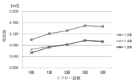
- FIG.3 and FIG.4 The result of having measured the change of the resistance of a shield film by changing the reflow frequency in the shield film of an Example and a comparative example is shown in FIG.3 and FIG.4.
- 240 degreeC reflow was performed for 25 seconds per time.
- FIG. 3 shows the measurement results of the example
- FIG. 4 shows the measurement results of the comparative example.
- the measurement result of the resistance value characteristic it is shown that the resistance of the example is lower than that of the comparative example, and the grounding to the ground line can be strengthened.
- the number of layers in the comparative example is equal to the number of laminated ground members. It is increasing. That is, in the embodiment, since there are few contacts in the direction in which electricity is transmitted, it is possible to reduce the resistance.
- FIG. 5 is a diagram showing a system configuration used in the KEC method.
- the system used in the KEC method includes an electromagnetic wave shielding effect measuring device 211, a spectrum analyzer 221, an attenuator 222 that attenuates 10 dB, an attenuator 223 that attenuates 3 dB, and a preamplifier 224.
- the spectrum analyzer 221 was U3741 manufactured by Advantest Corporation.
- HP 8447F manufactured by Agilent Technologies was used.
- FIG. 5A shows an electric field wave shield effect evaluation apparatus 211a
- FIG. 5B shows a magnetic field wave shield effect evaluation apparatus 211b.
- the electric field wave shield effect evaluation apparatus 211a is provided with two measuring jigs 213 facing each other. Between the measurement jigs 213 and 213, the shield film 1 (measurement sample) to be measured is installed so as to be sandwiched.
- the measurement jig 213 includes a TEM cell (Transverse Electro (Magnetic Cell) dimension distribution is incorporated, and the structure is divided symmetrically in a plane perpendicular to the transmission axis direction. However, in order to prevent a short circuit from being formed due to the insertion of the measurement sample 1, the plate-like center conductor 214 is arranged with a gap between each measurement jig 213.
- the electric field wave shield effect evaluation apparatus 211a is provided with two measuring jigs 215 facing each other. The shield film 1 to be measured is installed so as to be sandwiched between the measurement jigs 215 and 215.
- the magnetic field shield effect evaluation apparatus 211b uses a shield-type circular loop antenna 216 for the measurement jig 215 and combines it with a 90 ° square metal plate.
- the structure is such that a quarter of the antenna is exposed to the outside.
- a signal output from the spectrum analyzer 221 is input to the transmission side measurement jig 213 or the measurement jig 215 via the attenuator 222. Then, the signal is received by the measurement jig 213 or the measurement jig 215 on the receiving side and the signal via the attenuator 223 is amplified by the preamplifier 224, and then the signal level is measured by the spectrum analyzer 221.
- the spectrum analyzer 221 outputs the attenuation when the shield film is installed in the electromagnetic wave shielding effect measuring device 211 with reference to the state where the shield film is not installed in the electromagnetic wave shielding effect measuring device 211.
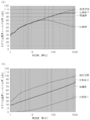
- the measurement result of the electric field wave shield performance by the KEC method is shown in FIG. 6 (a), and the measurement result of the magnetic field wave shield performance is shown in FIG. 6 (b).
- the Example has implement
- the Example has implement
- the embodiment can realize the magnetic field wave shielding performance comparable to the conventional one, though it is a simple and thin configuration.
- FIG. 3 This system includes a data generator 341, an oscilloscope 342, a sampling module 343 attached to the oscilloscope 342, and a pair of connection boards 332.
- the data generator 341 used was 81133A manufactured by Agilent Technologies.
- the oscilloscope 342, DSC8200 manufactured by Tektronix was used.
- the sampling module 343 used was 80E03 manufactured by Tektronix.
- connection board 332 has an input terminal and an output terminal, and the shield film 1 to be measured floats in the air between the pair of connection boards 332.
- the eye pattern is observed by connecting to the data generator 341 and the sampling module 343.
- the input amplitude was 150 mV / side (300 mVdiff).
- the data pattern was PRBS23. The measurement was performed in an atmosphere at a temperature of 25 ° C. and a relative humidity of 30 to 50%.
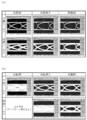
- FIG. 8A shows the measurement results observed with the oscilloscope 342 when the bit rate is 1.0 Gbps
- FIG. 8B shows the measurement results when the bit rate is 3.0 Gbps.
- the eye pattern of the comparative example is more vacant than the embodiment, regardless of the single-sided shield or the double-sided shield. That is, it turned out that an Example is a shield film suitable for high-speed signal processing rather than Comparative Examples 1 and 2.
- the bending durability of the shield film was evaluated by changing the type of plating.
- a nickel plating layer having a thickness of 0.5 ⁇ m or more, a rolled copper foil layer having a layer thickness of 18 ⁇ m, and a polyimide film layer having a layer thickness of 12.5 ⁇ m were used as the shield film.
- Two types of nickel plating layers were used: soft nickel plating formed with a sulfamic acid bath and nickel plating formed with a watt bath.
- a 10 mm ⁇ 100 mm specimen was used.
- the shield film subjected to the soft nickel plating was cracked at the sixth time.
- the shield film that was nickel-plated in the Watt bath was cracked at the third time.
Landscapes
- Engineering & Computer Science (AREA)
- Microelectronics & Electronic Packaging (AREA)
- Physics & Mathematics (AREA)
- Electromagnetism (AREA)
- Shielding Devices Or Components To Electric Or Magnetic Fields (AREA)
- Structure Of Printed Boards (AREA)
Description
また、特許文献1には、シールドフィルムにグランド部材を埋設するという方法も記載されているが、シールドフィルムの側部からグランド部材をはみ出して露出させる必要があり、シールドフィルムの適用する携帯機器の形状を制限してしまうという問題があった。
また、シールドプリント配線板が小型化された場合、グランド部材の取り付けが困難になるという問題がある。
さらに、グランド部材をシールド層に積層させる必要があるため、薄型化が制限されるという問題がある。
上記の構成によれば、良好な加工性及び導電性を得ることができると共に、安価なシールドフィルムを得ることができる。
上記の構成によれば、良好なシールド特性を得ることができる。
上記の構成によれば、導電性を有したまま金属層の表面の劣化を軽減することができる。
上記の構成によれば、使用環境による金属層表面の劣化を軽減し、抵抗値等の電気特性を長期に亘って安定させることができる。これにより、安定した電磁波シールド効果を得ることができる。
上記の構成によれば、良好な変形特性を得ることができる。
上記の構成によれば、良好な変形特性を得ることができる。
プリント配線板に貼り付けられる一般的なシールドフィルムは黒色である。上記構成によれば、一般的なシールドフィルムを貼り付けない本発明のような場合でも従来の見た目に準じることができる。
上記構成によれば、最小幅が10mm以下であっても、グランド接続可能であり、シールド特性が良好なプリント配線板を提供することができる。
上記構成によれば、グランド部材が接続可能な金属層は、プリント配線板上のグランド用配線パターンにも接続することが可能となっている。これにより、金属層は、さらに電磁波シールド特性が向上される。
図1に示すように、シールドフィルム1は、信号回路6a(信号用配線パターン)が形成されたベースフィルム5(ベース部材)と、信号回路6aを覆って当該ベースフィルム5上の全面に設けられる絶縁フィルム7と、を有するフレキシブルプリント配線板8(プリント配線板)に設けられている。シールドフィルム1は、絶縁フィルム7上の全面に積層される導電性接着剤層15と、導電性接着剤層15上の全面に積層された金属層11と、を有する。
上記のような構成のシールドプリント配線板110は、各ブロック部120が、ブロック部120よりも細長く形成された接続部130によって接続される構成となっている。また、各ブロック部120には配線パターンに接続される各種電子部品が設けられ、接続部130に形成された配線パターンによって各電子部品を電気的に接続するようになっている。
また、シールドプリント配線板110は、各接続部130が屈曲されて筐体等に立体的に収納されると共に、各ブロック部130に形成された貫通孔を介してねじ等が螺合されることにより筐体等に固設される。
このように、シールドプリント配線板110は、接続部130のような幅が細く形成された領域を有している。シールドフィルムにおいてこのように細く形成された箇所においてもグランド接続する必要があるが、本実施形態のシールドフィルムであれば、例えば、接続部130の最小幅が10mm以下に形成されるような場合であっても、金属層がプリント配線板を覆う導電性接着剤層の全面に積層されているため、接続部130のいずれの箇所であっても外部グランドに接続可能である。
尚、シールドプリント配線板(シールドフィルム)の形状は、上記のようなブロック部が接続部によって接続される形状に限定されない。例えば、多角形、円形、楕円形、これらに凹凸を加えた形状、及び、これらに貫通孔又は貫通孔を形成するための突出部を加えた形状、等であってもよい。また、上述のように、最小幅が10mm以下に形成されてもよい。
次に、図1に示す各層について具体的に説明する。
本実施形態の金属層11は、銅を主成分とした金属箔で形成されている。即ち、金属層11は、最外面にめっき層12を有している。
尚、金属層は、この構成に限定されない。例えば、金属層は、2層以上であってもよい。
尚、金属層11は、圧延加工により形成された金属箔であることに限定されず、特殊電解めっき法によって、金属箔と同様に結晶が面方向に広がった構造を有するように形成された金属層であってもよい。これにより、圧延加工と同様に、良好な形状保持性を得ることができる。
めっき層12は、金属層11の全面に積層されている。例えば、めっき層12は、電解めっき法、無電解めっき法等によって形成される。めっき層12が最外面に形成されることにより、導電性を有したまま金属層11の表面の劣化を軽減することができる。めっき層12の金属材料として、例えば、金、ニッケル、銅、銀、錫、パラジウム、アルミニウム、クロム、チタン、亜鉛、及び、これらの材料の何れか1つ以上を含む合金などを挙げることができる。
尚、めっき層12の厚みの下限は、0.1μmが好ましく、0.3μmがより好ましい。また、めっき層12の厚みの上限は、5μmが好ましく、3μmがより好ましい。
また、一般的なシールドフィルムの色である黒に合わせて、めっき層の少なくとも表面が黒色に形成されていることが好ましい。例えば、めっき層12は、ニッケル錫合金めっき等により黒色のめっきに形成されていても良いし、めっき表面に黒色の導電性接着剤層を形成してもよい。
導電性接着剤層15は、厚み方向のみだけ電気的な導電状態が確保された異方導電性を有する異方導電性接着剤層が、伝送特性やコストの面から好ましいが、これに限定されない。例えば、導電性接着剤層15は、厚み方向および幅方向、長手方向からなる三次元の全方向に電気的な導電状態が確保された等方導電性を有する等方導電性接着剤層であってもよい。導電性接着剤層15は、接着剤に難燃剤や導電性フィラーが添加されて形成される。
シールドフィルム1をFPC(フレキシブルプリント配線板)に適用する場合、導電性接着剤層15の厚みの下限は、2μmが好ましく、3μmがより好ましい。また、導電性接着剤層15の厚みの上限は、15μmが好ましく、9μmがより好ましい。
次に、図1を用いて、上記のシールドフィルム1をFPC(フレキシブルプリント配線板)に貼り付けしたシールドプリント配線板10について説明する。尚、本実施形態では、シールドフィルムをFPCに貼り付けした場合について説明するがこれに限定されない。例えば、COF(チップオンフレックス)、RF(リジットフレックスプリント板)、多層フレキシブル基板、リジット基板などに利用できる。
プリント回路6の表面は、信号回路6aとグランド回路6bとからなり、グランド回路6bの少なくとも一部(絶縁除去部6c)を除いて、絶縁フィルム7によって被覆されている。また、絶縁フィルム7は、内部にシールドフィルム1の導電性接着剤層15の一部が流れ込んでいる絶縁除去部7aを有している。これにより、グランド回路6bと金属層11とが電気的に接続される。
そして、信号回路6a及びグランド回路6bは、導電性材料をエッチング処理することにより配線パターンが形成される。また、グランド回路6bは、グランド電位を保つパターンのことを指す。即ち、ベースフィルム5には、グランド用配線パターンであるグランド回路6bが形成されている。
より具体的に言えば、シールドプリント配線板10は、信号用配線パターン(信号回路6a)とグランド用配線パターン(グランド回路6b)とが形成されたベース部材(ベースフィルム5)と、信号用配線パターンを覆うと共にグランド用配線パターンの少なくとも一部を露出した状態でベース部材上に設けられた絶縁フィルム7と、を有している。そして、絶縁フィルム7上に、シールドフィルム1が、導電性接着剤層15の接着により貼り付けされている。
尚、ベースフィルム5の厚みの下限は、10μmが好ましく、20μmがより好ましい。また、ベースフィルム5の厚みの上限は、60μmが好ましく、40μmがより好ましい。
また、絶縁フィルム7の厚みの下限は、10μmが好ましく、20μmがより好ましい。また、絶縁フィルム7の厚みの上限は、60μmが好ましく、40μmがより好ましい。
この結果、信号回路6aの領域とグランド回路6bの領域との両方に対し、2種類に区分することなくシールドフィルム1を構成することができるため、フレキシブルプリント配線板8上の信号回路6a及びグランド回路6bの配設態様は制限されず小型化及び低コスト化を可能にすることができる。
本実施形態のシールドフィルム1の製造方法の一例について説明する。
先ず、金属層11には、市販の銅箔(6μm)を用いる。銅箔をさらに薄くする場合は、エッチングにより薄くすることが好ましい。エッチングは、銅箔に対してポリエチレンテレフタレート等のフィルムを貼り付けた状態で行う。さらに、金属層11の一方面については、めっき処理によってめっき層12を形成する。そして、金属層11の他方面に導電性接着剤を塗布して導電性接着剤層15を形成する。このように、シールドフィルム1が作製される。
先ず、フレキシブルプリント配線板8の絶縁フィルム7に対して、レーザー加工などによって穴を開けて絶縁除去部7aを形成する。これにより、グランド回路6bの一部の領域が絶縁除去部7aにおいて外部に露出される。
そして、フレキシブルプリント配線板8の絶縁フィルム7上に、シールドフィルム1の導電性接着剤層15が接着される。この接着時においては、ヒーターによってシールドフィルム1を加熱しながら、プレス機によって上下方向からフレキシブルプリント配線板8とシールドフィルム1とを圧着する。これにより、シールドフィルム1の導電性接着剤層15がヒーターの熱によって軟らかくなり、プレス機の加圧によって絶縁フィルム7上に接着される。この際、柔らかくなった導電性接着剤層15の一部が絶縁除去部7aに充填される。従って、絶縁除去部7aで露出していたグランド回路6bの一部が充填された導電性接着剤層15に接着する。これにより、グランド回路6bと金属層11とが導電性接着剤層15を介して電気的に接続されることになる。
実施例としては、図1に示すような構成のシールドプリント配線板10を用いた。シールドフィルムのめっき層は、層厚0.1μmのニッケルめっき上に0.03μmの金めっきを行ったものである。シールドフィルムの金属層は、層厚6μmの圧延銅箔である。シールドフィルムの導電性接着剤層は、異方導電性を有するものを用い、層厚6μmに形成した。
また、比較例としては、従来のシールドフィルムの保護層を剥離し、シールド層にグランド部材を接続したものを用いた。図9に示すように、比較例のシールドフィルム501は、一部が剥離された層厚5μmの絶縁層(保護層)504、層厚0.1μmの銀で形成された金属層503、及び、層厚10μmの導電性接着剤層502が順次積層されてなるものである。また、グランド部材520は、層厚0.1μmのニッケルめっき上に0.03μmの金めっき処理を行って形成しためっき層523、層厚6μmの圧延銅箔522、及び、層厚6μmの異方導電性接着剤層521が順次積層されてなるものである。
また、シールドフィルムを貼り付けるフレキシブルプリント配線板には、いずれも、図1に示すような構成のものを用いた。具体的に、フレキシブルプリント配線板は、プリント回路が設けられた層厚12.5μmのポリイミド製のベースフィルム5に、層厚18μmのグランド用銅配線パターンと信号用銅配線パターンとからなるプリント回路6が形成され、さらに層厚15μmの接着剤層と層厚12.5μmのポリイミド製フィルム層で層厚27.5μmの絶縁フィルム7が形成されたものである。
尚、比較例は、保護層504の一部が剥離されてグランド部材520が取り付けられた箇所を測定対象とした。
先ず、一定の荷重下におけるシールドフィルムの抵抗を測定した。図2に示すように、シールドプリント配線板10の上に、夫々荷重1W(9.8N)をかねた電極となる2つの電極端子113a、113bが配置されている。両電極端子113a、113bはそれぞれ抵抗測定装置14の電流入出力端子にそれぞれ接続されている。尚、電極端子113a、113bは、それぞれL×Lmm2の正方形の底面を有する四角柱である。また、両電極端子電極端子113a、113bは距離Lだけ離れている。ここで、Lは約10mmである。
ここで、実施例のシールドフィルム1(図1参照)と、比較例のシールドフィルム501(図9参照)との層構造を比較すると、比較例はグランド部材を積層している分だけ層数が多くなっている。即ち、実施例では、電気が伝わる方向に接点が少ないため、抵抗を低くすることが可能となっている。
次に、シールドフィルムの電界波及び磁界波シールド特性について、一般社団法人KEC関西電子工業振興センターで開発された電磁波シールド効果測定装置211(電界波シールド効果評価装置211a、磁界波シールド効果評価装置211b)を用いたKEC法により評価した。図5は、KEC法で用いられるシステムの構成を示す図である。KEC法で用いられるシステムは、電磁波シールド効果測定装置211と、スペクトラムアナライザ221と、10dBの減衰を行うアッテネータ222と、3dBの減衰を行うアッテネータ223と、プリアンプ224とで構成される。
尚、スペクトラムアナライザ221には、株式会社アドバンテスト社製のU3741を用いた。また、アジレントテクノロジーズ社製のHP8447Fを用いた。
電界波シールド効果評価装置211aには、2つの測定治具213が対向して設けられている。この測定治具213・213間に、測定対象のシールドフィルム1(測定試料)が挟持されるように設置される。測定治具213には、TEMセル(Transverse Electro
Magnetic Cell)の寸法配分が取り入れられ、その伝送軸方向に垂直な面内で左右対称に分割した構造になっている。但し、測定試料1の挿入によって短絡回路が形成されることを防止するために、平板状の中心導体214は各測定治具213との間に隙間を設けて配置されている。
また、電界波シールド効果評価装置211aには、2つの測定治具215が対向して設けられている。この測定治具215・215間に、測定対象のシールドフィルム1が挟持されるように設置される。磁界波シールド効果評価装置211bは、磁界波成分の大きな電磁界を発生させるために、測定治具215にシールド型円形ループ・アンテナ216を使用し、90度角の金属板と組み合わせて、ループ・アンテナの1/4の部分が外部に出ている構造になっている。
次に、シールドフィルムの出力波形特性について、図7に示すような、システム構成を用いて評価した。このシステムは、データジェネレータ341と、オシロスコープ342と、オシロスコープ342に取り付けられたサンプリングモジュール343と1対の接続用基板332とで構成される。
尚、データジェネレータ341には、アジレントテクノロジーズ社製の81133Aを用いた。オシロスコープ342には、テクトロニクス社製のDSC8200を用いた。またサンプリングモジュール343は、テクトロニクス社製の80E03を用いた。
次に、シールドフィルムの曲げ耐久特性について、めっきの種類を変えて評価した。シールドフィルムには、0.5μm以上のニッケルめっき層、層厚18μmの圧延銅箔層、及び、層厚12.5μmのポリイミド製フィルム層を用いた。ニッケルめっき層には、スルファミン酸浴により形成したソフトニッケルめっき、及び、ワット浴により形成したニッケルめっきの2種類を用いた。また、10mm×100mmの試験体を用いた。
5 ベースフィルム
6 プリント回路
6a 信号回路
6b グランド回路
6c 絶縁除去部
7 絶縁フィルム
7a 絶縁除去部
8 フレキシブルプリント配線板
10 シールドプリント配線板
11 金属層
12 めっき層
15 導電性接着剤層
Claims (11)
- 信号用配線パターンが形成されたベース部材と、前記信号用配線パターンを覆って当該ベース部材上の全面に設けられる絶縁フィルムと、を有するプリント配線板に設けられるシールドフィルムであって、
前記絶縁フィルム上の全面に積層される導電性接着剤層と、
前記導電性接着剤層上の全面に積層された金属層と、
を有することを特徴とするシールドフィルム。 - 前記金属層は、銅を主成分とした金属箔であることを特徴とする請求項1に記載のシールドフィルム。
- 前記金属層は、層厚が2μm~12μmに加工されていることを特徴とする請求項2に記載のシールドフィルム。
- 前記金属層は、表面に防錆処理が施されていることを特徴とする請求項1乃至3の何れか1項に記載のシールドフィルム。
- 前記金属層上の全面に積層されためっき層をさらに有していることを特徴とする請求項1乃至3の何れか1項に記載のシールドフィルム。
- 前記めっき層は、少なくとも一層がソフトニッケルで形成された層であることを特徴とする請求項5に記載のシールドフィルム。
- 前記めっき層は、少なくとも一層が軟質金めっきで形成された層であることを特徴とする請求項5又は6に記載のシールドフィルム。
- 前記めっき層は、少なくとも一層が表面が黒色に形成されていることを特徴とする請求項5乃至7の何れか1項に記載のシールドフィルム。
- 最小幅が10mm以下に形成されていることを特徴とする請求項1乃至8の何れか1項に記載のシールドフィルム。
- 前記プリント配線板は、前記ベース部材にグランド用配線パターンが形成され、前記絶縁フィルムが前記グランド用配線パターンの少なくとも一部を露出するものであり、
前記導電性接着剤層は、前記グランド配線パターンの露出箇所と接続されることを特徴とする請求項1乃至9の何れか1項に記載のシールドフィルム。 - 前記プリント配線板と、前記プリント配線板に設けられた請求項1乃至10の何れか1項に記載のシールドフィルムと、を有することを特徴とするシールドプリント配線板。
Priority Applications (3)
| Application Number | Priority Date | Filing Date | Title |
|---|---|---|---|
| CN201380036819.7A CN104429173B (zh) | 2012-07-13 | 2013-06-05 | 屏蔽膜及屏蔽印刷线路板 |
| KR20157003877A KR20150038074A (ko) | 2012-07-13 | 2013-06-05 | 차폐 필름, 및 차폐 프린트 배선판 |
| US14/414,514 US9888619B2 (en) | 2012-07-13 | 2013-06-05 | Shield film and shield printed wiring board |
Applications Claiming Priority (2)
| Application Number | Priority Date | Filing Date | Title |
|---|---|---|---|
| JP2012157785A JP6240376B2 (ja) | 2012-07-13 | 2012-07-13 | シールドフィルム、及び、シールドプリント配線板 |
| JP2012-157785 | 2012-07-13 |
Publications (1)
| Publication Number | Publication Date |
|---|---|
| WO2014010342A1 true WO2014010342A1 (ja) | 2014-01-16 |
Family
ID=49915815
Family Applications (1)
| Application Number | Title | Priority Date | Filing Date |
|---|---|---|---|
| PCT/JP2013/065616 Ceased WO2014010342A1 (ja) | 2012-07-13 | 2013-06-05 | シールドフィルム、及び、シールドプリント配線板 |
Country Status (6)
| Country | Link |
|---|---|
| US (1) | US9888619B2 (ja) |
| JP (1) | JP6240376B2 (ja) |
| KR (1) | KR20150038074A (ja) |
| CN (1) | CN104429173B (ja) |
| TW (1) | TW201406278A (ja) |
| WO (1) | WO2014010342A1 (ja) |
Cited By (13)
| Publication number | Priority date | Publication date | Assignee | Title |
|---|---|---|---|---|
| CN105120643A (zh) * | 2015-06-30 | 2015-12-02 | 保定乐凯新材料股份有限公司 | 一种用于快速加工的热塑性电磁波屏蔽膜 |
| TWI552435B (zh) * | 2015-08-17 | 2016-10-01 | 啟碁科技股份有限公司 | 天線結構及其製造方法 |
| JP2017059802A (ja) * | 2015-09-17 | 2017-03-23 | 東洋インキScホールディングス株式会社 | 電磁波シールド用積層体、電磁波シールド積層体、電子機器およびその製造方法 |
| JP2017059708A (ja) * | 2015-09-17 | 2017-03-23 | 東洋インキScホールディングス株式会社 | 電磁波シールドシートおよびプリント配線板 |
| JP2017059801A (ja) * | 2015-09-17 | 2017-03-23 | 東洋インキScホールディングス株式会社 | 電磁波シールド用積層体、電磁波シールド積層体、電子機器およびその製造方法 |
| JP2017079218A (ja) * | 2015-10-19 | 2017-04-27 | 東洋インキScホールディングス株式会社 | 電磁波シールドシートおよびプリント配線板 |
| US20170345789A1 (en) * | 2014-12-12 | 2017-11-30 | Meiko Electronics Co., Ltd. | Encapsulated Circuit Module, And Production Method Therefor |
| KR20180062438A (ko) * | 2015-02-02 | 2018-06-08 | 토요잉크Sc홀딩스주식회사 | 전자파 차폐 시트, 프린트 배선판 및 전자 기기 |
| CN108377609A (zh) * | 2018-04-25 | 2018-08-07 | 维沃移动通信有限公司 | 一种屏蔽膜、柔性电路板组件及移动终端 |
| CN108391370A (zh) * | 2018-04-24 | 2018-08-10 | 维沃移动通信有限公司 | 一种屏蔽膜、电路板及移动终端 |
| JP2019511185A (ja) * | 2016-09-23 | 2019-04-18 | アップル インコーポレイテッドApple Inc. | 無線電力伝送システムのための電磁シールド |
| US10910862B2 (en) | 2016-09-23 | 2021-02-02 | Apple Inc. | Electromagnetic shielding for wireless power transfer systems |
| CN113973485A (zh) * | 2020-07-24 | 2022-01-25 | 广州方邦电子股份有限公司 | 一种膜及线路板 |
Families Citing this family (32)
| Publication number | Priority date | Publication date | Assignee | Title |
|---|---|---|---|---|
| JP6303597B2 (ja) * | 2014-02-28 | 2018-04-04 | 東洋インキScホールディングス株式会社 | 電子部品モジュールの製造方法 |
| JP6372122B2 (ja) * | 2014-03-20 | 2018-08-15 | 東洋インキScホールディングス株式会社 | 電子機器の製造方法 |
| JP2016081959A (ja) * | 2014-10-10 | 2016-05-16 | シチズン電子株式会社 | 発光装置及びその製造方法 |
| JP6426067B2 (ja) * | 2015-08-06 | 2018-11-21 | 日本メクトロン株式会社 | 多層フレキシブルプリント配線板およびその製造方法 |
| KR102608700B1 (ko) * | 2015-12-25 | 2023-11-30 | 타츠타 전선 주식회사 | 전자파 차폐 필름 및 그의 제조 방법 |
| JP2017212274A (ja) * | 2016-05-24 | 2017-11-30 | タツタ電線株式会社 | 電磁波シールドフィルム、およびそれを備えたシールドプリント配線板 |
| CN106170175B (zh) * | 2016-08-04 | 2019-04-26 | 同健(惠阳)电子有限公司 | 一种高保真高频线路板 |
| CN106604523A (zh) * | 2016-11-13 | 2017-04-26 | 惠州市大亚湾科翔科技电路板有限公司 | 一种陶瓷基高频覆铜板 |
| JP6554618B2 (ja) * | 2017-02-13 | 2019-07-31 | タツタ電線株式会社 | シールドプリント配線板及びシールドプリント配線板の製造方法 |
| US10477738B2 (en) | 2017-03-06 | 2019-11-12 | Laird Technologies, Inc. | Board level shields and systems and methods of applying board level shielding |
| TWI658753B (zh) * | 2017-03-17 | 2019-05-01 | 易鼎股份有限公司 | Signal anti-attenuation shielding structure of flexible circuit board |
| US10080277B1 (en) * | 2017-03-17 | 2018-09-18 | Advanced Flexible Circuits Co., Ltd. | Attenuation reduction structure for flexible circuit board |
| US20210059042A1 (en) * | 2017-07-10 | 2021-02-25 | Tatsuta Electric Wire & Cable Co., Ltd. | Electromagnetic Shielding Film and Shielded Printed Wiring Board Including the Same |
| US10159143B1 (en) * | 2017-07-31 | 2018-12-18 | Advanced Flexible Circuits Co., Ltd. | Attenuation reduction structure for flexible circuit board |
| KR101982036B1 (ko) * | 2017-12-27 | 2019-05-24 | 한화큐셀앤드첨단소재 주식회사 | 전자파 차폐필름, 이를 포함하는 전자파 차폐 적층체, 및 이들의 제조방법 |
| CN108427520A (zh) * | 2018-04-02 | 2018-08-21 | 业成科技(成都)有限公司 | 触控面板与其制造方法 |
| CN110769671B (zh) * | 2018-07-27 | 2024-04-26 | 广州方邦电子股份有限公司 | 电磁屏蔽膜、线路板及电磁屏蔽膜的制备方法 |
| CN110769673B (zh) * | 2018-07-27 | 2024-04-23 | 广州方邦电子股份有限公司 | 电磁屏蔽膜、线路板及电磁屏蔽膜的制备方法 |
| CN110769674B (zh) * | 2018-07-27 | 2024-04-23 | 广州方邦电子股份有限公司 | 电磁屏蔽膜、线路板及电磁屏蔽膜的制备方法 |
| CN110769675B (zh) * | 2018-07-27 | 2024-04-26 | 广州方邦电子股份有限公司 | 电磁屏蔽膜、线路板及电磁屏蔽膜的制备方法 |
| CN110769676B (zh) * | 2018-07-27 | 2024-05-31 | 广州方邦电子股份有限公司 | 电磁屏蔽膜、线路板及电磁屏蔽膜的制备方法 |
| CN110769672B (zh) * | 2018-07-27 | 2024-04-23 | 广州方邦电子股份有限公司 | 电磁屏蔽膜、线路板及电磁屏蔽膜的制备方法 |
| TWI673501B (zh) * | 2018-09-05 | 2019-10-01 | 矽品精密工業股份有限公司 | 測試治具 |
| US10694620B1 (en) * | 2019-04-02 | 2020-06-23 | Microsoft Technology Licensing, Llc | Method and apparatus for circuit board noise shielding and grounding |
| KR102843874B1 (ko) * | 2019-04-09 | 2025-08-08 | 삼성전자주식회사 | 연성 인쇄 회로 기판 및 그 연성 인쇄 회로 기판을 포함하는 전자 장치 |
| CN112492738A (zh) * | 2019-09-12 | 2021-03-12 | 广州方邦电子股份有限公司 | 一种线路板及电子设备 |
| KR102472342B1 (ko) * | 2020-02-10 | 2022-11-30 | 진테크 주식회사 | 열반응성 점착제층을 구비한 전자파 차폐용 캐리어 금속극박 및 이의 제조방법 |
| JP6881663B2 (ja) * | 2020-08-25 | 2021-06-02 | 東洋インキScホールディングス株式会社 | フレキシブルプリント配線板、フレキシブルプリント配線板の製造方法及び電子部材 |
| WO2022158450A1 (ja) * | 2021-01-19 | 2022-07-28 | 昭和電工マテリアルズ株式会社 | 導電性部材、電子装置の製造方法、接続構造体、及び、電子装置 |
| CN115623693A (zh) * | 2021-07-13 | 2023-01-17 | 庆鼎精密电子(淮安)有限公司 | 具有排气功能的线路板及其制作方法 |
| US12278206B2 (en) * | 2022-01-27 | 2025-04-15 | Airoha Technology (HK) Limited | Semiconductor package with conductive adhesive that overflows for return path reduction and associated method |
| TW202604224A (zh) * | 2024-03-29 | 2026-01-16 | 日商拓自達電線股份有限公司 | 電磁波屏蔽膜 |
Citations (8)
| Publication number | Priority date | Publication date | Assignee | Title |
|---|---|---|---|---|
| JPS63173389A (ja) * | 1987-01-13 | 1988-07-16 | 古河電気工業株式会社 | フレキシブルプリント配線板の接続端子部のメツキ処理方法 |
| WO2007032087A1 (ja) * | 2005-09-16 | 2007-03-22 | Fujitsu Limited | 携帯端末装置 |
| JP2007294918A (ja) * | 2006-03-29 | 2007-11-08 | Tatsuta System Electronics Kk | シールドフィルム及びシールドプリント配線板 |
| JP2008120081A (ja) * | 2006-11-11 | 2008-05-29 | Joinset Co Ltd | 軟性金属積層フィルム及びその製造方法 |
| JP2011066329A (ja) * | 2009-09-18 | 2011-03-31 | Tatsuta Electric Wire & Cable Co Ltd | シールドフィルム、そのシールドフィルムを有するシールド配線板、シールドフィルムにおけるグランド接続方法 |
| WO2011121801A1 (ja) * | 2010-03-30 | 2011-10-06 | Jx日鉱日石金属株式会社 | 電磁波シールド用複合体 |
| WO2012008260A1 (ja) * | 2010-07-15 | 2012-01-19 | Jx日鉱日石金属株式会社 | 銅箔複合体 |
| JP4883432B2 (ja) * | 2010-05-31 | 2012-02-22 | 東洋紡績株式会社 | フレキシブル金属張積層体 |
Family Cites Families (9)
| Publication number | Priority date | Publication date | Assignee | Title |
|---|---|---|---|---|
| JPH06283574A (ja) * | 1993-03-30 | 1994-10-07 | Seiko Epson Corp | ニッケルめっき、ニッケルめっき方法及びtab用フレキシブル回路基板 |
| JPH0711477A (ja) * | 1993-06-28 | 1995-01-13 | Electroplating Eng Of Japan Co | 貴金属めっき品 |
| JP3498386B2 (ja) * | 1994-10-19 | 2004-02-16 | 住友電気工業株式会社 | シールド付きフレキシブル配線板及びその製造方法 |
| JPH1155014A (ja) | 1997-07-29 | 1999-02-26 | Tokin Corp | アンテナ |
| JP2003086907A (ja) * | 2001-06-29 | 2003-03-20 | Tatsuta Electric Wire & Cable Co Ltd | シールドフレキシブルプリント配線板 |
| JP4324029B2 (ja) * | 2004-06-25 | 2009-09-02 | 住友電工プリントサーキット株式会社 | 金属膜及び接着剤層を有する積層フィルム及びその製造方法 |
| TWI270341B (en) | 2005-03-02 | 2007-01-01 | Cateron Technology Co Ltd | Electronic assembly unit with conductive film, conductive film and method of making the same thereof |
| CN102241950A (zh) * | 2010-05-14 | 2011-11-16 | 3M创新有限公司 | 电磁屏蔽胶带 |
| JP5541319B2 (ja) | 2012-07-12 | 2014-07-09 | トヨタ自動車株式会社 | 被覆活物質の製造方法 |
-
2012
- 2012-07-13 JP JP2012157785A patent/JP6240376B2/ja active Active
-
2013
- 2013-06-05 US US14/414,514 patent/US9888619B2/en active Active
- 2013-06-05 KR KR20157003877A patent/KR20150038074A/ko not_active Ceased
- 2013-06-05 WO PCT/JP2013/065616 patent/WO2014010342A1/ja not_active Ceased
- 2013-06-05 CN CN201380036819.7A patent/CN104429173B/zh active Active
- 2013-06-24 TW TW102122319A patent/TW201406278A/zh unknown
Patent Citations (8)
| Publication number | Priority date | Publication date | Assignee | Title |
|---|---|---|---|---|
| JPS63173389A (ja) * | 1987-01-13 | 1988-07-16 | 古河電気工業株式会社 | フレキシブルプリント配線板の接続端子部のメツキ処理方法 |
| WO2007032087A1 (ja) * | 2005-09-16 | 2007-03-22 | Fujitsu Limited | 携帯端末装置 |
| JP2007294918A (ja) * | 2006-03-29 | 2007-11-08 | Tatsuta System Electronics Kk | シールドフィルム及びシールドプリント配線板 |
| JP2008120081A (ja) * | 2006-11-11 | 2008-05-29 | Joinset Co Ltd | 軟性金属積層フィルム及びその製造方法 |
| JP2011066329A (ja) * | 2009-09-18 | 2011-03-31 | Tatsuta Electric Wire & Cable Co Ltd | シールドフィルム、そのシールドフィルムを有するシールド配線板、シールドフィルムにおけるグランド接続方法 |
| WO2011121801A1 (ja) * | 2010-03-30 | 2011-10-06 | Jx日鉱日石金属株式会社 | 電磁波シールド用複合体 |
| JP4883432B2 (ja) * | 2010-05-31 | 2012-02-22 | 東洋紡績株式会社 | フレキシブル金属張積層体 |
| WO2012008260A1 (ja) * | 2010-07-15 | 2012-01-19 | Jx日鉱日石金属株式会社 | 銅箔複合体 |
Cited By (17)
| Publication number | Priority date | Publication date | Assignee | Title |
|---|---|---|---|---|
| US20170345789A1 (en) * | 2014-12-12 | 2017-11-30 | Meiko Electronics Co., Ltd. | Encapsulated Circuit Module, And Production Method Therefor |
| US10665568B2 (en) * | 2014-12-12 | 2020-05-26 | Meiko Electronics Co., Ltd. | Encapsulated circuit module, and production method therefor |
| KR102291975B1 (ko) | 2015-02-02 | 2021-08-23 | 토요잉크Sc홀딩스주식회사 | 전자파 차폐 시트, 프린트 배선판 및 전자 기기 |
| KR20180062438A (ko) * | 2015-02-02 | 2018-06-08 | 토요잉크Sc홀딩스주식회사 | 전자파 차폐 시트, 프린트 배선판 및 전자 기기 |
| CN105120643A (zh) * | 2015-06-30 | 2015-12-02 | 保定乐凯新材料股份有限公司 | 一种用于快速加工的热塑性电磁波屏蔽膜 |
| TWI552435B (zh) * | 2015-08-17 | 2016-10-01 | 啟碁科技股份有限公司 | 天線結構及其製造方法 |
| JP2017059801A (ja) * | 2015-09-17 | 2017-03-23 | 東洋インキScホールディングス株式会社 | 電磁波シールド用積層体、電磁波シールド積層体、電子機器およびその製造方法 |
| JP2017199934A (ja) * | 2015-09-17 | 2017-11-02 | 東洋インキScホールディングス株式会社 | 電磁波シールド用積層体、電磁波シールド積層体、電子機器およびその製造方法 |
| JP2017059708A (ja) * | 2015-09-17 | 2017-03-23 | 東洋インキScホールディングス株式会社 | 電磁波シールドシートおよびプリント配線板 |
| JP2017059802A (ja) * | 2015-09-17 | 2017-03-23 | 東洋インキScホールディングス株式会社 | 電磁波シールド用積層体、電磁波シールド積層体、電子機器およびその製造方法 |
| JP2017079218A (ja) * | 2015-10-19 | 2017-04-27 | 東洋インキScホールディングス株式会社 | 電磁波シールドシートおよびプリント配線板 |
| JP2019511185A (ja) * | 2016-09-23 | 2019-04-18 | アップル インコーポレイテッドApple Inc. | 無線電力伝送システムのための電磁シールド |
| US10910862B2 (en) | 2016-09-23 | 2021-02-02 | Apple Inc. | Electromagnetic shielding for wireless power transfer systems |
| CN108391370A (zh) * | 2018-04-24 | 2018-08-10 | 维沃移动通信有限公司 | 一种屏蔽膜、电路板及移动终端 |
| CN108391370B (zh) * | 2018-04-24 | 2020-02-18 | 维沃移动通信有限公司 | 一种屏蔽膜、电路板及移动终端 |
| CN108377609A (zh) * | 2018-04-25 | 2018-08-07 | 维沃移动通信有限公司 | 一种屏蔽膜、柔性电路板组件及移动终端 |
| CN113973485A (zh) * | 2020-07-24 | 2022-01-25 | 广州方邦电子股份有限公司 | 一种膜及线路板 |
Also Published As
| Publication number | Publication date |
|---|---|
| US20150250080A1 (en) | 2015-09-03 |
| JP2014022460A (ja) | 2014-02-03 |
| US9888619B2 (en) | 2018-02-06 |
| CN104429173B (zh) | 2018-05-04 |
| KR20150038074A (ko) | 2015-04-08 |
| JP6240376B2 (ja) | 2017-11-29 |
| TW201406278A (zh) | 2014-02-01 |
| CN104429173A (zh) | 2015-03-18 |
Similar Documents
| Publication | Publication Date | Title |
|---|---|---|
| JP6240376B2 (ja) | シールドフィルム、及び、シールドプリント配線板 | |
| JP6321535B2 (ja) | シールドフィルム、シールドプリント配線板、及び、シールドフィルムの製造方法 | |
| TWI627881B (zh) | 屏蔽膜及屏蔽印刷電路板 | |
| US8144482B2 (en) | Circuit board device, wiring board interconnection method, and circuit board module device | |
| CN102316664B (zh) | 柔性电路板及其制作方法 | |
| US20110308841A1 (en) | Coverlay film, method for manufacturing coverlay film, and flexible printed wiring board | |
| JP2011159879A (ja) | シールド付フレキシブルプリント配線板、その製造方法、および電子機器 | |
| TWI602478B (zh) | 形狀保持膜、及具備該形狀保持膜的形狀保持型撓性電路板 | |
| KR20160124344A (ko) | 연성회로기판 및 그 제조방법 | |
| JP2017212472A (ja) | シールドフィルム、及び、シールドプリント配線板 | |
| KR20100129619A (ko) | 전자파 차폐 필름이 구비된 플렉시블 피씨비 | |
| JP6406453B2 (ja) | 樹脂基板、樹脂基板の製造方法 | |
| WO2007064138A1 (en) | Electromagnetic waves and static electricity screening structure at circuit | |
| HK1183198A (en) | Shield film, sheilded printed board and method for manufacturing shield film | |
| JP2006352050A (ja) | 回路基板 |
Legal Events
| Date | Code | Title | Description |
|---|---|---|---|
| 121 | Ep: the epo has been informed by wipo that ep was designated in this application |
Ref document number: 13816102 Country of ref document: EP Kind code of ref document: A1 |
|
| NENP | Non-entry into the national phase |
Ref country code: DE |
|
| ENP | Entry into the national phase |
Ref document number: 20157003877 Country of ref document: KR Kind code of ref document: A |
|
| WWE | Wipo information: entry into national phase |
Ref document number: 14414514 Country of ref document: US |
|
| 122 | Ep: pct application non-entry in european phase |
Ref document number: 13816102 Country of ref document: EP Kind code of ref document: A1 |