WO2014003110A1 - ダイヤモンド単結晶及びその製造方法並びに単結晶ダイヤモンド工具 - Google Patents
ダイヤモンド単結晶及びその製造方法並びに単結晶ダイヤモンド工具 Download PDFInfo
- Publication number
- WO2014003110A1 WO2014003110A1 PCT/JP2013/067632 JP2013067632W WO2014003110A1 WO 2014003110 A1 WO2014003110 A1 WO 2014003110A1 JP 2013067632 W JP2013067632 W JP 2013067632W WO 2014003110 A1 WO2014003110 A1 WO 2014003110A1
- Authority
- WO
- WIPO (PCT)
- Prior art keywords
- single crystal
- diamond
- diamond single
- less
- wavelength
- Prior art date
Links
Images


Classifications
-
- C—CHEMISTRY; METALLURGY
- C30—CRYSTAL GROWTH
- C30B—SINGLE-CRYSTAL GROWTH; UNIDIRECTIONAL SOLIDIFICATION OF EUTECTIC MATERIAL OR UNIDIRECTIONAL DEMIXING OF EUTECTOID MATERIAL; REFINING BY ZONE-MELTING OF MATERIAL; PRODUCTION OF A HOMOGENEOUS POLYCRYSTALLINE MATERIAL WITH DEFINED STRUCTURE; SINGLE CRYSTALS OR HOMOGENEOUS POLYCRYSTALLINE MATERIAL WITH DEFINED STRUCTURE; AFTER-TREATMENT OF SINGLE CRYSTALS OR A HOMOGENEOUS POLYCRYSTALLINE MATERIAL WITH DEFINED STRUCTURE; APPARATUS THEREFOR
- C30B25/00—Single-crystal growth by chemical reaction of reactive gases, e.g. chemical vapour-deposition growth
- C30B25/02—Epitaxial-layer growth
- C30B25/18—Epitaxial-layer growth characterised by the substrate
- C30B25/186—Epitaxial-layer growth characterised by the substrate being specially pre-treated by, e.g. chemical or physical means
-
- B—PERFORMING OPERATIONS; TRANSPORTING
- B23—MACHINE TOOLS; METAL-WORKING NOT OTHERWISE PROVIDED FOR
- B23B—TURNING; BORING
- B23B27/00—Tools for turning or boring machines; Tools of a similar kind in general; Accessories therefor
- B23B27/14—Cutting tools of which the bits or tips or cutting inserts are of special material
- B23B27/148—Composition of the cutting inserts
-
- C—CHEMISTRY; METALLURGY
- C30—CRYSTAL GROWTH
- C30B—SINGLE-CRYSTAL GROWTH; UNIDIRECTIONAL SOLIDIFICATION OF EUTECTIC MATERIAL OR UNIDIRECTIONAL DEMIXING OF EUTECTOID MATERIAL; REFINING BY ZONE-MELTING OF MATERIAL; PRODUCTION OF A HOMOGENEOUS POLYCRYSTALLINE MATERIAL WITH DEFINED STRUCTURE; SINGLE CRYSTALS OR HOMOGENEOUS POLYCRYSTALLINE MATERIAL WITH DEFINED STRUCTURE; AFTER-TREATMENT OF SINGLE CRYSTALS OR A HOMOGENEOUS POLYCRYSTALLINE MATERIAL WITH DEFINED STRUCTURE; APPARATUS THEREFOR
- C30B25/00—Single-crystal growth by chemical reaction of reactive gases, e.g. chemical vapour-deposition growth
- C30B25/02—Epitaxial-layer growth
- C30B25/18—Epitaxial-layer growth characterised by the substrate
- C30B25/20—Epitaxial-layer growth characterised by the substrate the substrate being of the same materials as the epitaxial layer
-
- C—CHEMISTRY; METALLURGY
- C30—CRYSTAL GROWTH
- C30B—SINGLE-CRYSTAL GROWTH; UNIDIRECTIONAL SOLIDIFICATION OF EUTECTIC MATERIAL OR UNIDIRECTIONAL DEMIXING OF EUTECTOID MATERIAL; REFINING BY ZONE-MELTING OF MATERIAL; PRODUCTION OF A HOMOGENEOUS POLYCRYSTALLINE MATERIAL WITH DEFINED STRUCTURE; SINGLE CRYSTALS OR HOMOGENEOUS POLYCRYSTALLINE MATERIAL WITH DEFINED STRUCTURE; AFTER-TREATMENT OF SINGLE CRYSTALS OR A HOMOGENEOUS POLYCRYSTALLINE MATERIAL WITH DEFINED STRUCTURE; APPARATUS THEREFOR
- C30B29/00—Single crystals or homogeneous polycrystalline material with defined structure characterised by the material or by their shape
- C30B29/02—Elements
- C30B29/04—Diamond
-
- C—CHEMISTRY; METALLURGY
- C30—CRYSTAL GROWTH
- C30B—SINGLE-CRYSTAL GROWTH; UNIDIRECTIONAL SOLIDIFICATION OF EUTECTIC MATERIAL OR UNIDIRECTIONAL DEMIXING OF EUTECTOID MATERIAL; REFINING BY ZONE-MELTING OF MATERIAL; PRODUCTION OF A HOMOGENEOUS POLYCRYSTALLINE MATERIAL WITH DEFINED STRUCTURE; SINGLE CRYSTALS OR HOMOGENEOUS POLYCRYSTALLINE MATERIAL WITH DEFINED STRUCTURE; AFTER-TREATMENT OF SINGLE CRYSTALS OR A HOMOGENEOUS POLYCRYSTALLINE MATERIAL WITH DEFINED STRUCTURE; APPARATUS THEREFOR
- C30B30/00—Production of single crystals or homogeneous polycrystalline material with defined structure characterised by the action of electric or magnetic fields, wave energy or other specific physical conditions
-
- C—CHEMISTRY; METALLURGY
- C30—CRYSTAL GROWTH
- C30B—SINGLE-CRYSTAL GROWTH; UNIDIRECTIONAL SOLIDIFICATION OF EUTECTIC MATERIAL OR UNIDIRECTIONAL DEMIXING OF EUTECTOID MATERIAL; REFINING BY ZONE-MELTING OF MATERIAL; PRODUCTION OF A HOMOGENEOUS POLYCRYSTALLINE MATERIAL WITH DEFINED STRUCTURE; SINGLE CRYSTALS OR HOMOGENEOUS POLYCRYSTALLINE MATERIAL WITH DEFINED STRUCTURE; AFTER-TREATMENT OF SINGLE CRYSTALS OR A HOMOGENEOUS POLYCRYSTALLINE MATERIAL WITH DEFINED STRUCTURE; APPARATUS THEREFOR
- C30B31/00—Diffusion or doping processes for single crystals or homogeneous polycrystalline material with defined structure; Apparatus therefor
- C30B31/20—Doping by irradiation with electromagnetic waves or by particle radiation
- C30B31/22—Doping by irradiation with electromagnetic waves or by particle radiation by ion-implantation
-
- B—PERFORMING OPERATIONS; TRANSPORTING
- B23—MACHINE TOOLS; METAL-WORKING NOT OTHERWISE PROVIDED FOR
- B23B—TURNING; BORING
- B23B2226/00—Materials of tools or workpieces not comprising a metal
- B23B2226/31—Diamond
-
- Y—GENERAL TAGGING OF NEW TECHNOLOGICAL DEVELOPMENTS; GENERAL TAGGING OF CROSS-SECTIONAL TECHNOLOGIES SPANNING OVER SEVERAL SECTIONS OF THE IPC; TECHNICAL SUBJECTS COVERED BY FORMER USPC CROSS-REFERENCE ART COLLECTIONS [XRACs] AND DIGESTS
- Y10—TECHNICAL SUBJECTS COVERED BY FORMER USPC
- Y10T—TECHNICAL SUBJECTS COVERED BY FORMER US CLASSIFICATION
- Y10T407/00—Cutters, for shaping
- Y10T407/24—Cutters, for shaping with chip breaker, guide or deflector
-
- Y—GENERAL TAGGING OF NEW TECHNOLOGICAL DEVELOPMENTS; GENERAL TAGGING OF CROSS-SECTIONAL TECHNOLOGIES SPANNING OVER SEVERAL SECTIONS OF THE IPC; TECHNICAL SUBJECTS COVERED BY FORMER USPC CROSS-REFERENCE ART COLLECTIONS [XRACs] AND DIGESTS
- Y10—TECHNICAL SUBJECTS COVERED BY FORMER USPC
- Y10T—TECHNICAL SUBJECTS COVERED BY FORMER US CLASSIFICATION
- Y10T428/00—Stock material or miscellaneous articles
- Y10T428/30—Self-sustaining carbon mass or layer with impregnant or other layer
Definitions
- the present invention includes a cutting tool, an anti-wear tool, a precision tool, a heat radiating member, a diamond single crystal used for a semiconductor device substrate, an optical component, and the like, a method of manufacturing the same, a turning process of an automobile part, a mirror surface process of an optical part, a spherical process,
- the present invention relates to a single crystal diamond tool used for fine grooving and the like, particularly to a single crystal diamond cutting tool.
- diamond Since diamond has many excellent properties such as high hardness, high thermal conductivity, high light transmittance, wide band gap, etc., it is widely used as a material for various tools, optical parts, semiconductors, electronic parts, In the future, it will be even more important.
- single crystal diamond tools are used in mirror finishing and precision machining of non-ferrous metals such as aluminum alloys and copper alloys used in automobiles, optical equipment, electronic equipment, and plastics such as acrylic. Since it is generally more expensive than a sintered diamond tool that is often used in relatively rough machining, for example, as disclosed in Patent Document 2, a single crystal diamond tool with improved performance while suppressing cost has been proposed.
- the CVD diamond single crystal according to the prior art has low toughness compared to natural products and high-temperature high-pressure synthetic Ib products. .
- a single crystal diamond tool using a CVD diamond single crystal according to the prior art is more likely to be cracked or chipped at the cutting edge than a tool using a natural product or a high temperature / high pressure synthetic Ib product. This problem has been one of the factors that hinder the spread of CVD diamond single crystals.
- the object of the present invention is to solve such problems of the prior art, achieve both high hardness and high toughness, and is easy to work at the time of tool production, and is equivalent to or better than tools using natural products or high-temperature / high-pressure synthetic Ib products. It is an object of the present invention to provide a diamond single crystal, a single crystal diamond tool, and a method for producing a diamond single crystal that realizes this, which are less likely to crack or chip and have a long lifetime and high fracture resistance during cutting.
- a diamond single crystal according to the present invention is a diamond single crystal synthesized by a chemical vapor synthesis method, and has an absorption coefficient of light having a wavelength of 350 nm of 25 cm ⁇ 1 or more and 80 cm ⁇ 1 or less.
- Single crystal (5)
- the method for producing a diamond single crystal according to the present invention includes a non-carbon ion on a main surface of a diamond single crystal seed substrate whose main surface is a surface having an off angle of 7 ° or less from the ⁇ 100 ⁇ plane.
- the ratio N C / N H of hydrogen molecule number N H is not more than 10% to 40%, and the ratio N N / N C of the number of molecules N C molecule containing a nitrogen molecule number N N and carbon And a step of homoepitaxially growing the diamond single crystal under a synthesis condition of 0.1% to 10% and a seed substrate temperature T of 850 ° C. to less than 1000 ° C.
- the number of molecules containing carbon refers to the number of molecules of methane if the molecule containing carbon is methane gas, and the number of molecules of ethane if ethane gas is used.
- the diamond single crystal according to the present invention is a single crystal diamond tool whose blade edge is composed of a diamond single crystal, and a rake face has an absorption coefficient of light of a wavelength of 350 nm of the diamond single crystal of 25 cm ⁇ . This is a single crystal diamond tool formed on the main surface side of less than 1 .
- both high hardness and high toughness are achieved, and it is easy to process at the time of tool production, cracking and chipping are less likely to occur at the same level as tools using natural products and high-temperature high-pressure synthetic Ib products, It is possible to provide a diamond single crystal having a high fracture resistance, a single crystal diamond tool, and a method for producing a diamond single crystal that realizes this.
- the diamond single crystal of the present invention is a diamond single crystal synthesized by a chemical vapor synthesis method, and has an absorption coefficient of light having a wavelength of 350 nm of 25 cm ⁇ 1 or more and 80 cm ⁇ 1 or less.
- the diamond single crystal according to (1) preferably has an absorption coefficient of 30 cm ⁇ 1 or more and 80 cm ⁇ 1 or less.
- Diamond single crystals whose light absorption coefficient (wavelength 350 nm) is 25 cm ⁇ 1 or more and 80 cm ⁇ 1 or less obtained from transmittance, which is the result of measurement with an ultraviolet-visible spectrophotometer, are natural products or high-temperature / high-pressure synthetic Ib products.
- a diamond single crystal having an absorption coefficient of light with a wavelength of 350 nm of 30 cm ⁇ 1 or more and 80 cm ⁇ 1 or less is easier to process than a natural product or a high-temperature high-pressure synthetic Ib product, and is less susceptible to cracking or chipping. It was found that can be obtained.
- the diamond single crystal of the present invention is a diamond single crystal produced by a vapor phase synthesis method, and is composed of two or more diamond single crystal layers having different absorption coefficients of light having a wavelength of 350 nm,
- the absorption coefficient of light of 350 nm wavelength of the diamond single crystal layer including the main surface is less than 25 cm ⁇ 1
- the absorption coefficient of light of 350 nm wavelength of the diamond single crystal layer including the other main surface is 25 cm. ⁇ 1 or more and 80 cm ⁇ 1 or less
- any one of the two or more diamond single crystal layers is a diamond single crystal having an absorption coefficient of light having a wavelength of 350 nm that does not exceed 80 cm ⁇ 1 .
- the absorption coefficient of light of 350 nm wavelength of the diamond single crystal layer including one main surface is less than 25 cm ⁇ 1
- the absorption coefficient of light of 350 nm wavelength of the diamond single crystal layer including the other main surface is 25 cm. ⁇ 1 or more and 80 cm ⁇ 1 or less, and if any of the two or more diamond single crystal layers has a light absorption coefficient of 350 nm that does not exceed 80 cm ⁇ 1 , the absorption coefficient is low. It has been found that the effect of achieving both high hardness and high toughness is remarkable in the diamond single crystal layer, and characteristics superior to the high-temperature and high-pressure synthetic Ib diamond single crystal usually used in tool applications can be obtained.
- the diamond single crystal described in (3) above is a diamond single crystal having two or more diamond single crystal layers, and has an absorption coefficient of 25 cm ⁇ 1 of light having a wavelength of 350 nm including one main surface.
- the absorption coefficient of light having a wavelength of 350 nm is directed from a diamond single crystal layer having a wavelength of 350 nm to a diamond single crystal layer having a wavelength of 350 nm including the other main surface of 25 cm ⁇ 1 or more and 80 cm ⁇ 1 or less. Is preferably monotonically increasing.
- the absorption coefficient of light having a wavelength of 350 nm monotonously increases toward a diamond single crystal layer having an absorption coefficient of light having a wavelength of 350 nm of 25 cm ⁇ 1 or more and 80 cm ⁇ 1 or less, the effect is more remarkable. I found out.
- ions other than carbon are implanted into the main surface of a diamond single crystal seed substrate whose main surface is a surface whose off angle from the ⁇ 100 ⁇ plane is within 7 °.
- the present inventors have conducted ion implantation from the main surface of a diamond single crystal seed substrate having a main surface whose off angle is within 7 ° from the just ⁇ 100 ⁇ plane. Ions other than carbon are implanted deeper than the main surface using a device, etc., and the crystal structure of the diamond single crystal is destroyed and graphitized to reduce the transmittance of light having a wavelength of 800 nm.
- a diamond single crystal obtained by homoepitaxial growth of a diamond single crystal under a synthesis condition of 850 ° C. or higher and lower than 1000 ° C. has higher toughness than a conventional diamond single crystal, and can be used for natural products and high-temperature / high-pressure synthesis.
- the pressure is preferably 30 Torr or more and 400 Torr or less, and more preferably 65 Torr or more and less than 110 Torr.
- a molecule containing carbon in a gas phase is further obtained by chemical vapor synthesis on a growth surface obtained by homoepitaxially growing the diamond single crystal.
- the ratio N C / N H between the number of molecules N C and the number of hydrogen molecules N H is greater than 0% and less than 10%, or the ratio between the number of nitrogen molecules N N and the number of molecules N C containing carbon N N
- the pressure is preferably 30 Torr or more and 400 Torr or less, and more preferably 110 Torr or more and 400 Torr or less.
- the present inventors have found that hardness and toughness differ when the absorption coefficient of light having a wavelength of 350 nm of a diamond single crystal produced by a vapor phase synthesis method is different. Furthermore, it has been found that if the absorption coefficient of light having a wavelength of 350 nm is 80 cm ⁇ 1 or less, the hardness decreases and the toughness improves as the absorption coefficient increases. On the other hand, since a diamond single crystal can be epitaxially grown on a diamond single crystal seed substrate by vapor phase synthesis, it has a plurality of layers whose absorption coefficients are steeply different in the growth direction, that is, the thickness direction if the synthesis conditions are changed. A diamond single crystal can be formed.
- a diamond single crystal having two or more layers having different absorption coefficients that is, different hardness and toughness can be formed.
- the diamond single crystal produced in this way has a low absorption coefficient and high hardness, like a Japanese sword, but on the low toughness layer side, the underlying absorption coefficient is high and low hardness but a high toughness layer. Since it supplements toughness, it has been found that both high hardness and high toughness, which cannot be achieved by a single layer, are compatible.
- N N / N C of the number of molecules N C molecule containing a nitrogen molecule number N N and carbon is less than 10% 0.1%, and, the seed substrate temperature T 850 °C or more and less than 1000 °C
- N C / N H is less than 0% from large 10%
- N N / A diamond single crystal was homoepitaxially grown under a synthesis condition in which either N C was less than 0.1% and the seed substrate temperature T was less than 1000 ° C., and then the seed substrate was grown on the seed substrate.
- the diamond single crystal is obtained by electrochemically etching and separating a graphite layer formed by laser slicing or ion implantation.
- the diamond single crystal produced in this way has higher hardness and toughness than the conventional CVD diamond single crystal in the single crystal layer with a lower absorption coefficient.
- the diamond single crystal is processed more than natural products and high-temperature high-pressure synthetic Ib products. It was found that cracking and chipping are easy to occur.
- the off angle is preferably within 3 °, and more preferably within 0.5 °.
- the main surface of the diamond single crystal seed substrate has an off-angle within 3 °, more preferably within 0.5 ° from the just ⁇ 100 ⁇ plane, so that island growth and step flow, which are growth modes during homoepitaxial growth, are performed.
- step flow growth which is a cause of low toughness, can be further suppressed than within an off angle of 7 °, so it has been found that it is easier to process than natural products and high-temperature high-pressure synthetic Ib products, and cracks and chips are less likely to occur. .
- the method for producing a diamond single crystal according to any one of (5) to (7) above includes a step of separating the seed substrate and the diamond single crystal homoepitaxially grown on the seed substrate. Furthermore, it is preferable to include. After homoepitaxially growing a diamond single crystal on the seed substrate, the seed substrate and the diamond single crystal grown thereon are separated by electrochemical etching of a graphite layer formed by laser slicing or ion implantation. can do. By further including such a step of separating the seed substrate and the diamond single crystal, the seed substrate can be reused.
- a single crystal diamond tool of the present invention is a single crystal diamond tool comprising a cutting edge made of the diamond single crystal according to (3) or (4) above, wherein a rake face is 350 nm of the diamond single crystal.
- the single crystal diamond tool is formed on the main surface side having a light absorption coefficient of less than 25 cm ⁇ 1 .
- the diamond single crystal having a plurality of diamond single crystal layers with different absorption coefficients obtained as described above has a toughness that cannot be achieved with a single layer in the single crystal layer with a low absorption coefficient. High hardness and high toughness are compatible.
- the single crystal diamond tool of the present invention is a single crystal diamond tool in which a diamond single crystal is bonded to a tool shank, and the diamond single crystal is ion-implanted from a crystal surface on the side to be bonded to the shank.
- the single crystal diamond tool according to (10) is preferably a single crystal diamond cutting tool.
- the cutting is usually continued, but the surface roughness of the work material after the chipping is worse than that before the chipping.
- the surface roughness of the work material is small, that is, the degree of mirror finishing is often noted, so natural materials and high-temperature / high-pressure synthetic Ib can be used as materials with as few microscopic defects as possible.
- the product is used.
- high-temperature and high-pressure synthetic IIa products and CVD diamond single crystals tend to be relatively hard and brittle, and are therefore rarely used.
- the inventors of the present invention have made extensive studies in order to solve the above-mentioned problem that a CVD diamond single crystal that can be mass-produced at low cost is not so much used.
- a single crystal diamond tool is obtained by ion-implanting from a crystal plane to be bonded to a shank of a vapor-phase synthetic diamond single crystal and providing an ion-implanted layer at a position slightly deeper from the crystal plane, brazing is performed.
- the formed ion-implanted layer acting as an impact relaxation layer during cutting it has been found that cracks and chips are less likely to occur than in a tool using a natural product or a high-temperature high-pressure synthetic Ib product.
- the single crystal diamond tool of the present invention can improve tool performance such as fracture resistance while using the diamond single crystal as a tool tip. It has been found that the impact mitigating effect of the ion-implanted layer is particularly remarkable in a single crystal diamond cutting tool among single crystal diamond tools.
- the transmittance of light having a wavelength of 800 nm in the direction perpendicular to the ion implantation layer is It is preferable to change 10% or more before and after removing the ion implantation layer. If the ion-implanted layer is such that the transmittance of light having a wavelength of 800 nm in the direction perpendicular to the ion-implanted layer before and after removing the formed ion-implanted layer changes by 10% or more, the ion-implanted layer In this case, graphite produced by destroying the crystal structure of diamond gives a more effective impact relaxation effect.
- the diamond single crystal before the ion implantation processing is performed on a surface on which an ion implantation layer is formed.
- the absorption coefficient of light having a wavelength of 350 nm in the vertical direction is preferably 25 cm ⁇ 1 or more and 80 cm ⁇ 1 or less.
- the diamond single crystal In a diamond single crystal, if the absorption coefficient of light having a wavelength of 350 nm after removal of the ion-implanted layer is 25 cm ⁇ 1 or more and 80 cm ⁇ 1 or less, the diamond single crystal itself is a vacancy, a hydrogen atom, a nitrogen atom, or these As a result, the propagation of crystal fracture is likely to stop at the defect and the toughness is high, so that in combination with the ion-implanted layer according to the present invention, cracks and It has been found that chipping is difficult to occur.
- a diamond single crystal seed substrate 11 as shown in FIG. 1 is prepared.
- High-temperature and high-pressure synthetic diamond single crystal (HPHT) is preferable because it has relatively little crystal distortion, but may be CVD diamond single crystal (CVD).
- the thickness of the seed substrate is preferably 100 ⁇ m or more from the viewpoint of handling, and preferably 3 mm or less from the viewpoint of availability.
- the thickness of the seed substrate is a thickness measured in the vicinity of the center of the seed substrate main surface.
- the main surface 12 is a ⁇ 100 ⁇ plane, and the surface roughness Ra is preferably 40 nm or less. If Ra exceeds 40 nm, the diamond single crystal grown on the main surface may crack.
- the ⁇ 100 ⁇ plane is referred to when the off angle from the ⁇ 100 ⁇ just plane is within 7 °.
- the purpose of controlling the off-angle within 7 ° is to have low toughness among island growth and step flow growth, which are crystal growth modes when homoepitaxial growth on the main surface 12 is attempted to obtain a diamond single crystal.
- the diamond single crystal having an absorption coefficient of light having a wavelength of 350 nm of 25 cm ⁇ 1 or more and 80 cm ⁇ 1 or less of the present invention is suppressed by suppressing step flow growth, which causes undesired properties for diamond single crystal cutting tools. This is to realize the layer. If the off-angle is within 3 °, more preferably within 0.5 °, step flow growth is further suppressed, which is more desirable.
- the shape of the main surface 12 is typically a quadrangle, but may be a polygon or a circle.
- the optical characteristics of the diamond single crystal seed substrate 11 are such that the front main surface 12 and the back main surface for epitaxial growth of the diamond single crystal are roughened by ion etching or the like to increase Ra to 100 nm or more, or ion implantation or the like inside the crystal. It is preferable that the transmittance of light having a wavelength of 800 nm measured with an ultraviolet-visible spectrophotometer or the like is larger than 0% in a state where no defect is formed. A black seed substrate having a transmittance of 0% is not suitable because the crystal quality is poor and epitaxial growth does not occur even when vapor phase growth is performed.
- the implanted ion species, implantation energy, and implantation dose can be arbitrarily selected, but carbon that is an element constituting diamond
- implantation is performed at a temperature (850 ° C. or more and less than 1000 ° C.) when epitaxially growing a diamond single crystal layer having a light absorption coefficient of 350 nm wavelength of 25 cm ⁇ 1 or more and 80 cm ⁇ 1 or less in the next step. Since the crystal structure is restored to the previous surface state, it is not suitable.
- the temperature at the time of ion implantation is also less than 1000 ° C. Usually, even if injection is performed without temperature control, the temperature does not rise to 1000 ° C. at the time of injection, so the injection is performed without temperature control. Also, ion implantation processes that do not grow epitaxially are outside the scope of this patent.
- a surface state having a moderately destroyed structure can be efficiently realized in a low dose amount, that is, in a short time, when the implantation depth is shallow, so that the mass is heavy and the energy is preferably low.
- the implantation depth is preferably 1 ⁇ m or less, and more preferably 0.5 ⁇ m or less. More specific implantation conditions are, for example, 1 ⁇ 10 14 cm ⁇ 2 to 0.8 ⁇ 10 17 cm ⁇ 2 when the ion species is boron (mass number 11) and the energy is 175 keV, and the ion species is silicon (mass).
- Equation 28 phosphorus (mass number 31), sulfur (mass number 32), and energy of 300 keV, 1 ⁇ 10 13 cm ⁇ 2 to 5 ⁇ 10 16 cm ⁇ 2 can be used. Accordingly, silicon, phosphorus, and sulfur are more preferable than boron, carbon, and nitrogen.
- the decrease rate of the transmittance of light having a wavelength of 800 nm before and after ion implantation should be larger than 0%.
- the rate of decrease is preferably 10% or more, and more preferably 20% or more.
- Diamond single crystal growth Next, a diamond single crystal is grown on a seed substrate placed on a substrate holder of a diamond CVD growth furnace.
- a growth method a hot filament method, a combustion flame method, an arc jet method, or the like can be used, but a microwave plasma method is preferable in order to obtain diamond with less unintentional impurity contamination.
- the furnace pressure is maintained at 30 Torr to 400 Torr, and the frequency is 2.45 GHz ( ⁇ 50 MHz) or 915 MHz ( A diamond single crystal is epitaxially grown by generating plasma by applying a microwave of ⁇ 50 MHz) to an electric power of 100 to 60 kW and depositing active species on the seed substrate.
- the furnace pressure is preferably in the range of 30 Torr or more and 400 Torr or less, and more preferably in the range of 65 Torr or more and less than 110 Torr.
- hydrogen, methane, the ratio of introducing the gas of nitrogen in the synthesis gas phase, the ratio N C / N H number of molecules N C and a hydrogen molecule number N H of molecules containing carbon by 10% or more 40 % or less, the ratio N N / N C number of molecules N C molecule containing a nitrogen molecule number N N and carbon is 10% or less than 0.1%, by heating the seed substrate by plasma, the seed substrate temperature T Keeping the temperature at 850 ° C. or higher and lower than 1000 ° C. is a condition for synthesizing the diamond single crystal of the present invention.
- the diamond single crystal thus obtained has an absorption coefficient of light having a wavelength of 350 nm of 25 cm ⁇ 1 or more and 80 cm ⁇ 1 or less.
- the absorption coefficient is more preferably 30 cm ⁇ 1 or more and 80 cm ⁇ 1 or less, and further preferably 35 cm ⁇ 1 or more and 64 cm ⁇ 1 or less.
- N C / N H or N N / N C or T is out of the above range, the aforementioned ion implantation step is omitted, annealing at 1000 ° C. or more between the ion implantation step and the diamond single crystal growth step, etc. If the step of changing the surface state of the main surface is included, the absorption coefficient of light having a wavelength of 350 nm is less than 25 cm ⁇ 1 or greater than 80 cm ⁇ 1 .
- the growth process includes [1] an absorption coefficient of light having a wavelength of 350 nm of 25 cm ⁇ 1 or more and 80 cm ⁇ .
- the layers are formed in the order of a diamond single crystal layer having a wavelength of 1 or less and [2] a diamond single crystal layer having an absorption coefficient of light having a wavelength of 350 nm of less than 25 cm ⁇ 1 . This is because, in order to form the layer of [1], epitaxial growth on the surface of the substrate whose transmittance for light having a wavelength of 800 nm is reduced by ion implantation is essential.
- the layer referred to in the present invention refers to the case where the area that changes in the thickness direction change rate of the absorption coefficient at 1 cm ⁇ 1 /0.1 ⁇ m or more is divided into two in the thickness direction as an interface. It is defined as a region sandwiched between the interface and the main surface, or a region sandwiched between the interface and the interface, and even if there is a change in absorption coefficient of less than 1 cm ⁇ 1 /0.1 ⁇ m in the layer, the average absorption coefficient is It shall be calculated.
- each gas of hydrogen, methane, and nitrogen is used as described above.
- the ratio to be introduced into the synthesis gas phase 40% ratio N C / N H 10% or more of the number of molecules N C and a hydrogen molecule number N H of molecules containing carbon below, molecular nitrogen number N N and carbon
- the ratio N N / N C of the number N C of molecules containing N is 0.1% or more and 10% or less
- the seed substrate temperature T is kept at 850 ° C. or more and less than 1000 ° C. when the seed substrate is heated by plasma.
- the pressure during synthesis is preferably 30 Torr or more and 400 Torr or less, and more preferably 65 Torr or more and less than 110 Torr.
- N C / N H or N N / N C or T is out of the above range, the above-described ion implantation step is omitted, or annealing at 1000 ° C. or higher is performed between the ion implantation step and the main growth step.
- the absorption coefficient of light having a wavelength of 350 nm is less than 25 cm ⁇ 1 or greater than 80 cm ⁇ 1 .
- a layer having a different absorption coefficient from a layer having a certain absorption coefficient or a plurality of layers are stacked, one or more of the above three parameters are changed so that the absorption coefficient of light having a wavelength of 350 nm is 25 cm -1 or more, A layer of 80 cm -1 or less is synthesized.
- the synthesis may be stopped once, or the continuous synthesis may be performed by changing parameters. It is preferable to combine the stacked layers so that the absorption coefficient of light having a wavelength of 350 nm is smaller than that of the underlying layer, but the layers may be combined so as to increase.
- a layer having an absorption coefficient of light having a wavelength of 350 nm exceeding 80 cm ⁇ 1 is not synthesized. Further, by synthesizing the stacked layers so that the absorption coefficient of light having a wavelength of 350 nm is smaller than that of the underlying layer, the high hardness and high toughness characteristics of the diamond single crystal of the present invention can be remarkably extracted.
- a diamond single crystal layer having the absorption coefficient of light having a wavelength of 350 nm of [2] of less than 25 cm ⁇ 1 is grown.
- the ratio of introducing hydrogen, methane, and nitrogen gas into the synthesis gas phase is such that N C / N H is greater than 0% and less than 10%, or N N / N C is less than 0.1%.
- T is set as a synthesis condition of less than 1000 ° C.
- the diamond single crystal layer having a wavelength of 350 nm ⁇ 1 or more and 80 cm ⁇ 1 or less of the previously grown [1] 350 nm wavelength light is annealed and the absorption coefficient is 25 cm ⁇ . May change to less than 1 .
- growth is performed so as not to exceed the synthesis temperature of [1] grown previously so that the absorption coefficient of the layer formed in [1] does not change.
- the above three parameters are fixed. If N C / N H or N N / N C or T is outside the above range, the absorption coefficient of light having a wavelength of 350 nm is 25 cm ⁇ 1 or more, or a diamond / graphite composite layer in which graphite black spots are generated in the crystal is obtained. It is not preferable.
- synthesis is performed by changing one or more of the above three parameters, and finally a wavelength of 350 nm.
- a layer having a light absorption coefficient of less than 25 cm ⁇ 1 is synthesized.
- the synthesis may be stopped once, or the continuous synthesis may be performed by changing parameters.
- the main surface size of the obtained diamond single crystal is up to about 10 mm square, a method of separating the seed substrate and the diamond single crystal by laser slicing and polishing the laser cut surface can be applied. If the main surface size exceeds 10 mm square, the possibility of cracking the seed substrate or the diamond single crystal at the time of laser cutting increases, so the graphitized layer inside the seed substrate formed by the ion implantation process should be electrochemically etched. Thus, the seed substrate and the diamond single crystal can be separated. Alternatively, when it is not necessary to collect and reuse the seed substrate, the seed substrate may be removed by a technique such as polishing or reactive ion etching.
- the diamond single crystal separated from the seed substrate is polished so that the parallelism of both principal surfaces is within 10 ⁇ m and the surface roughness is 40 nm or less in order to accurately measure the absorption coefficient of light having a wavelength of 350 nm in each layer. Make adjustments as appropriate.
- the diamond single crystal thus obtained has a light absorption coefficient of 350 nm of 25 cm ⁇ 1 or more and 80 cm ⁇ 1 or less.
- it is composed of two or more diamond single crystal layers having different absorption coefficients of light having a wavelength of 350 nm, and light having a wavelength of 350 nm of the diamond single crystal layer including one main surface is formed.
- the absorption coefficient of light having a wavelength of 350 nm of the diamond single crystal layer including the other main surface is less than 25 cm ⁇ 1 and the absorption coefficient of light having a wavelength of 350 nm is not less than 25 cm ⁇ 1 and not more than 80 cm ⁇ 1 .
- the absorption coefficient ⁇ when the diamond single crystal is a single layer is calculated by the following equation.
- t ex t 2 / (1-r 2 ) ⁇ exp ( ⁇ L)
- absorption coefficient t ex external transmittance (transmittance measured with an ultraviolet-visible spectrophotometer, etc.)
- reflectivity 0.17
- L Distance between main faces and thickness of diamond single crystal
- the absorption coefficient in the case of a plurality of diamond single crystal layers is calculated by the following formula after repeating measurement of external transmittance and removal by outermost layer etching, polishing, or the like.
- t ex t 2 / (1-r 2 ) ⁇ exp ( ⁇ 1 L 1 ⁇ 2 L 2 ⁇ 3 L 3 ...
- t ex External transmittance (transmittance measured with an ultraviolet-visible spectrophotometer, etc.)
- reflectivity 0.17
- Absorption coefficient L n of the n-th grown diamond single crystal layer thickness of the n-th grown diamond single crystal layer
- the absorption coefficient of light having a wavelength of 350 nm is 0 cm ⁇ 1 .
- the crystal grows while incorporating impurities such as nitrogen, hydrogen, nickel, and vacancies into the crystal, and light is absorbed by these. To do.
- the cause of absorption of light having a wavelength of 350 nm in a diamond single crystal is considered to be due to a complex defect of nitrogen, vacancies, and hydrogen introduced into the crystal during CVD growth, and as this absorption increases,
- the thickness of the diamond single crystal is 1 mm, the apparent color is from brown to black.
- the temperature T is made lower than the synthesis condition described in the present invention, N C / N H is increased, or N N / N C is increased.
- N C / N H is increased, or N N / N C is increased.
- the inventors of the present invention have a relatively large number of such defects as compared with a CVD diamond single crystal according to the prior art, and a diamond single crystal that does not substantially include black spots of graphite.
- the toughness would be improved as a result of the crystal fracture propagation being stopped by the defects.
- conventional CVD diamond single crystals are more brittle than natural diamond single crystals and high-temperature and high-pressure synthetic Ib type diamond single crystals, and are difficult to machine into tools such as tools and end mills. We thought that the problem that cracks were likely to occur could be solved.
- defects such as nitrogen, fluorine, neon, silicon, phosphorus, sulfur, chlorine, argon, and arsenic are introduced on the surface to such an extent that epitaxial growth occurs.
- a diamond single crystal having an absorption coefficient of light having a wavelength of 350 nm of 25 cm ⁇ 1 or more and 80 cm ⁇ 1 or less and having high toughness and substantially not including black spots of graphite was realized. If the absorption coefficient is less than 25 cm ⁇ 1 , the toughness is insufficient, resulting in poor fracture resistance. On the other hand, if the absorption coefficient exceeds 80 cm ⁇ 1 , defects are included to the extent that it is difficult to maintain the diamond structure.
- the diamond single crystal of the present invention is a natural performance because it is called a diamond single crystal, but does not substantially contain graphite. “Substantially” means that a black spot cannot be found by observing the entire region of the diamond single crystal at a magnification of 20 times.
- the step flow growth which is the cause of low toughness
- step flow growth which is the cause of low toughness
- step flow growth which is the cause of low toughness
- step flow growth which is the cause of low toughness
- the main surface of the diamond single crystal seed substrate to be grown by CVD is within an off angle of 7 °, more preferably within 3 °, and even within 0.5 ° with respect to the just ⁇ 100 ⁇ plane.
- the absorption coefficient of light having a wavelength of 350 nm is 25 cm ⁇ 1 or more and 80 cm ⁇ 1 or less, and has a high toughness suitable for application to a cutting tool or the like.
- a diamond single crystal not encapsulating was realized.
- the absorption coefficient of light having a wavelength of 350 nm is more preferably 30 cm ⁇ 1 or more and 80 cm ⁇ 1 or less.
- the absorption coefficient of light having a wavelength of 350 nm is smaller than 25 cm ⁇ 1 as in the case of a conventional CVD diamond single crystal, the toughness is insufficient, resulting in poor fracture resistance.
- the wavelength of 350 nm was superimposed on a relatively high toughness diamond single crystal layer having a light absorption coefficient of 350 nm of 25 cm ⁇ 1 or more and 80 cm ⁇ 1 or less. If the diamond single crystal layer has a light absorption coefficient of less than 25 cm ⁇ 1 , the high toughness layer below compensates for the weakness of this layer, which is high hardness but low toughness, like a Japanese sword. It was found that both high hardness and high toughness that could not be achieved with a single layer were achieved.
- the diamond single crystal having a plurality of diamond single crystal layers having different absorption coefficients is composed of two or more diamond single crystal layers having different absorption coefficients of light having a wavelength of 350 nm, and one main surface is
- the diamond single crystal layer containing the light absorption coefficient of the wavelength of 350 nm is less than 25 cm ⁇ 1
- the diamond single crystal layer including the other main surface has the light absorption coefficient of the wavelength of 350 nm of 25 cm ⁇ 1 or more, and at 80 cm -1 or less
- the absorption coefficient of light of a wavelength of any 350nm of the two or more layers of single-crystal diamond layer is a diamond single crystal which does not exceed 80 cm -1.
- the absorption coefficient of light having a wavelength of 350 nm in each layer monotonically increases from one main surface to the other opposing main surface. It does not matter if it is random. In this case, however, the absorption coefficient of light having a wavelength of 350 nm does not exceed 80 cm ⁇ 1 in any of the plurality of intermediate layers sandwiched between the two main surfaces.
- a single crystal diamond tool 21 as shown in FIG. 2 is produced.
- the single crystal diamond tool 21 includes a diamond single crystal tip 22 using a diamond single crystal according to the present invention and a holder 23.
- the bottom surface 24 which is the ⁇ 100 ⁇ plane or ⁇ 110 ⁇ plane of the diamond single crystal chip 22 is joined to the notch formed at one end of the holder 23 by brazing or the like.
- the back surface 25 of the diamond single crystal chip is usually a ⁇ 100 ⁇ plane, but may be a ⁇ 110 ⁇ plane. By determining the crystal plane of the back surface 25, the crystal orientation of the diamond single crystal chip 22 with respect to the holder 23 is determined.
- the bottom surface 24 of the diamond single crystal chip 22 is a main surface on the side (25 cm ⁇ 1 or more and 80 cm ⁇ 1 or less) having a large absorption coefficient of light having a wavelength of 350 nm of the diamond single crystal according to the present invention. Accordingly, the rake face is on the side with a smaller absorption coefficient (side less than 25 cm ⁇ 1 ).
- the thickness of the absorption coefficient layer including the rake face is preferably 100 ⁇ m or less. By setting it as such thickness, the high hardness and toughness in a rake face like a Japanese sword appear more remarkably.
- the single crystal diamond tool according to the present invention as described above has both high hardness and high toughness, which could not be realized by a conventional diamond single crystal. Therefore, since it has higher hardness than a cutting tool using a conventional high-temperature and high-pressure synthetic Ib type diamond single crystal, it has excellent wear resistance and a long life. Moreover, since it is tougher than the cutting tool using the conventional CVD diamond single crystal, it is excellent in fracture resistance. Since the occurrence of microchipping during cutting is small, the surface roughness of the work material surface after cutting is small, and a smoother mirror finish can be obtained.
- the single crystal diamond tool according to the embodiment of the present invention is not particularly limited as long as it is used by joining a diamond single crystal to a tool shank, and examples thereof include a cutting tool, a dresser, and an end mill. Of these, a cutting tool is preferable.
- the single crystal diamond cutting tool 31 includes a diamond single crystal tip 32 and a holder 33 which is a shank.
- the bottom surface 34 which is the ⁇ 100 ⁇ surface or ⁇ 110 ⁇ surface of the diamond single crystal chip 32 is joined to the notch formed at one end of the holder 33 by brazing or the like.
- the back surface 35 is usually a ⁇ 100 ⁇ plane, but may be a ⁇ 110 ⁇ plane.
- an ion implantation layer 36 is usually formed at a position within a depth of 50 ⁇ m, more preferably within 30 ⁇ m, and even more preferably within 10 ⁇ m from a bottom surface 34 which is a surface to be bonded to a shank. Yes.
- the implanted ions When ions are implanted into a crystal, the implanted ions have a concentration distribution in the depth direction in the crystal.
- the depth of the ion implanted layer is the concentration of ions in the depth direction of the crystal. Means the peak position.
- the chip edge is more resistant to chipping by adopting such a configuration, in particular an ion implantation layer at a position slightly deeper than the bottom surface joined by brazing.
- the tool performance is equivalent or better than that of a cutting tool using a high-temperature and high-pressure synthetic Ib type diamond single crystal.
- the means for joining the diamond single crystal and the shank is not particularly limited, and any conventional known means may be used.
- the diamond single crystal used in the single crystal diamond tool according to the embodiment of the present invention is provided with an ion implantation layer.
- the ion implantation layer is formed by determining implantation conditions such as implantation ion species, implantation energy, implantation dose, and implantation angle.
- the purpose of ion implantation layer formation is to reduce the sudden impact that single crystal diamond tips receive during cutting by destroying the diamond crystal structure in the ion implantation layer formed by ion implantation and graphitizing it. This is because. Therefore, any ion species can be selected as long as it can be implanted into diamond.
- ion species such as phosphorus, boron, carbon, hydrogen, helium, nitrogen, oxygen, and argon may be implanted.
- the ion implantation conditions are selected so that the diamond structure is maintained on the outermost surface even after the ion implantation layer is formed.
- the position of the injection layer should be as deep as possible. More specifically, the concentration peak position in the crystal of the implanted ion species should be a depth of 0.20 ⁇ m or more, more preferably 0.30 ⁇ m or more, and still more preferably 0.50 ⁇ m or more. is there. By being in a deep position, joining to the shank by brazing is more reliable.
- the transmittance of light having a wavelength of 800 nm in the direction perpendicular to the ion implantation layer of the diamond single crystal is reduced with respect to the transmittance of the diamond single crystal without the ion implantation layer. It is preferable.
- the decrease in transmittance indicates that the diamond crystal structure was destroyed by ion implantation and graphite was formed, so that the ion implanted layer works effectively as an impact relaxation layer during cutting. .
- the transmittance is reduced by 10% or more. In this case, a more remarkable effect can be obtained as an impact relaxation layer.
- the method of confirming the transmittance decrease value by the ion-implanted layer is confirmed by one of the following two methods. Even if both are confirmed, the value normally obtained is the same, but if it is different, the larger value is adopted.
- ⁇ Confirmation method A of transmittance decrease value ⁇ 1. Remove the diamond single crystal from the single crystal diamond tool. 2. Remove the adhesive such as brazing material from the diamond single crystal. 3. The transmittance of the diamond single crystal is measured and set as an evaluation value [1]. 4). The ion implantation layer is removed by polishing or ion etching. 5. The transmittance of the diamond single crystal after removing the ion-implanted layer is measured and set as an evaluation value [2]. 6). The evaluation value [1] is subtracted from the evaluation value [2].
- ⁇ Confirmation method B of transmittance decrease value ⁇ 1. Remove the diamond single crystal from the single crystal diamond tool. 2. Remove the adhesive such as brazing material from the diamond single crystal. 3. It is confirmed that an ion implantation layer is formed using secondary ion mass spectrometry (SIMS) or the like. 4). The ion implantation conditions are confirmed using ion implantation simulation (TRIM) or the like. 5. Separately from the diamond single crystal removed from the single crystal diamond tool, a diamond single crystal plate having both major surfaces polished to a surface roughness of 40 nm or less is prepared. 6). 5. above. The transmittance of the diamond single crystal plate prepared in step 1 is measured and set as an evaluation value [1]. 7). 4. above. Under the ion implantation conditions confirmed in 5.
- the diamond single crystal used in the single crystal diamond tool according to the embodiment of the present invention has an ion implantation layer, but the absorption coefficient of light having a wavelength of 350 nm in a portion other than the ion implantation layer is 25 cm ⁇ 1 or more and 80 cm. -1 or less is preferable. That is, the vapor-phase synthetic diamond single crystal before being ion-implanted has an absorption coefficient of light having a wavelength of 350 nm perpendicular to the surface on which the ion-implanted layer is formed, of 25 cm ⁇ 1 or more and 80 cm ⁇ 1 or less. Preferably there is.
- the cause of absorption at 350 nm in a diamond single crystal is that there are many defects in the crystal that are a combination of vacancies, hydrogen atoms, and nitrogen atoms, and this occurs when cracks and chips occur. Propagation of crystal breakdown is relatively easily suppressed by defects. In other words, because it has high toughness, cracking and chipping occur when using such a diamond single crystal with an ion-implanted layer in a single crystal diamond tool, compared to a tool using a natural product or a high-temperature high-pressure synthetic Ib product. Hard to do.
- Such a diamond single crystal having an absorption coefficient of light having a wavelength of 350 nm of 25 cm ⁇ 1 or more and 80 cm ⁇ 1 or less can be produced by the CVD method as described above.
- Example 1-1 First, No. 1-01 to No. 1-22 diamond single crystal seed substrates shown in Table 1 were prepared. All of these sizes are 4 ⁇ 4 ⁇ 0.5 mm thick, and Nos. 1-01 to No. 1-13 are high-temperature and high-pressure synthetic type Ib diamond single crystals (HPHT Ib), No. 1-14 to No. 1 1-17 is a high-temperature high-pressure synthetic IIa type diamond single crystal (HPHT IIa), and Nos. 1-18 to No. 1-22 are vapor-phase synthetic diamond single crystal substrates (CVD).
- the surface roughness Ra of the main surface ( ⁇ 100 ⁇ surface) of 4 ⁇ 4 mm size was 40 nm or less.
- Table 1 shows the off-angle of the main surface of each seed substrate on which the diamond single crystal is grown in a later step and the transmittance of light having a wavelength of 800 nm.
- the transmittance of light with a wavelength of 800 nm of the seed substrate was lowered as shown in Table 1 by ion implantation from the main surface.
- ion implantation conditions phosphorus was used as an ion species, and an implantation energy of 100 to 800 keV and an implantation dose of 1 ⁇ 10 13 cm ⁇ 2 to 5 ⁇ 10 15 cm ⁇ 2 were selected.
- N C / N H is 10% or more and 40% or less
- N N / N C is 0.1% or more and 10% or less
- T is 850 ° C. or more and less than 1000 ° C.
- pressure P is 65 Torr or more and less than 110 Torr. did.
- the diamond single crystal is separated from the seed substrate by laser cutting, and the main surface on the growth surface side of the diamond single crystal and the main surface on the laser cutting surface side are polished, so that the main surface interval (thickness) is 1 mm.
- the parallelism between the main surfaces was within 10 ⁇ m and the surface roughness Ra was within 40 nm.
- the absorption coefficient of light with a wavelength of 350 nm of the diamond single crystal obtained from each seed substrate was measured using an ultraviolet-visible spectrophotometer. The results are shown in Table 1. That is, when the off-angle of the seed substrate is within 7 °, the absorption coefficient is 25 cm ⁇ 1 to 80 cm ⁇ 1 , and when the off-angle is within 0.5 °, the absorption coefficient is 30 cm ⁇ 1 to 80 cm ⁇ 1. It became. Further, as a result of observing the obtained diamond single crystal with a stereomicroscope, black spots due to graphite were not observed in any diamond single crystal.
- the absorption coefficient of light of wavelength 350nm is to produce a precise bytes diamond single crystal of 25 cm -1 ⁇ 80 cm -1, tried cutting performance evaluation.
- a cylindrical aluminum alloy AC4B was selected as the work material and the outer periphery thereof was turned by 50 km under the same conditions as the cutting speed of 600 m / min.
- the number was less than or equal to the precision bite made with the high-temperature and high-pressure synthetic Ib type diamond single crystal evaluated in the same manner.
- the diamond single crystal off-angle 0.5 ° absorption coefficient produced from the seed substrate is 30 cm -1 ⁇ 80 cm -1, missing number was less than the same number.
- the transmittance of light with a wavelength of 800 nm of the seed substrate was reduced as shown in Table 2, respectively.
- the ion implantation conditions were selected from the conditions in the range of the examples.
- a diamond single crystal was epitaxially grown on the ion-implanted main surface.
- a microwave plasma CVD apparatus is used, and hydrogen, methane, and nitrogen are introduced into the apparatus as raw material gases so that N C / N H , N N / N C , and T shown in Table 2 are obtained.
- the synthesis was performed by adjusting the amount of gas introduced.
- N C / N H was 10% or more and 40% or less
- N N / N C was 0.1% or more and 10% or less
- T was outside the range of 850 ° C. or more and less than 1000 ° C.
- the absorption coefficient of light with a wavelength of 350 nm of the diamond single crystal obtained from each seed substrate was measured using an ultraviolet-visible spectrophotometer.
- the results are shown in Table 2. That is, under the synthesis conditions, N C / N H was 10% or more and 40% or less, N N / N C was 0.1% or more and 10% or less, and T was outside the range of 850 ° C. or more and less than 1000 ° C.
- the absorption coefficient did not become 25 cm ⁇ 1 to 80 cm ⁇ 1 .
- the number of chips after the cutting evaluation of the precision tool was evaluated, but it was more than that produced by the high-temperature and high-pressure synthetic Ib type.
- the transmittance of light with a wavelength of 800 nm of the seed substrate was reduced as shown in Table 2, respectively.
- the ion implantation conditions were selected from the conditions in the range of the examples.
- a diamond single crystal was epitaxially grown on the ion-implanted main surface.
- a microwave plasma CVD apparatus is used, and hydrogen, methane, and nitrogen are introduced into the apparatus as raw material gases so that N C / N H , N N / N C , and T shown in Table 2 are obtained.
- the synthesis was performed by adjusting the amount of gas introduced.
- N C / N H was 10% or more and 40% or less
- N N / N C was 0.1% or more and 10% or less
- T was outside the range of 850 ° C. or more and less than 1000 ° C.
- the diamond single crystals obtained from the respective seed substrates contained graphite black spots as shown in Table 2. That is, under the synthesis conditions, N C / N H was 10% or more and 40% or less, N N / N C was 0.1% or more and 10% or less, and T was outside the range of 850 ° C. or more and less than 1000 ° C. Graphite sunspots occurred.
- Example 2-1 No. 2-01 to No. 2-22 diamond single crystal seed substrates shown in Table 3 were prepared. All these sizes are 4 ⁇ 4 ⁇ 0.5 mm thick, and Nos. 2-01 to No. 2-13 are high-temperature and high-pressure synthetic type Ib diamond single crystals (HPHT Ib), No. 2-14 to No. 2 2-17 is a high-temperature high-pressure synthetic diamond type IIa single crystal (HPHT IIa), and Nos. 2-18 to No. 2-22 are vapor-phase synthetic diamond single crystals (CVD).
- the surface roughness Ra of the main surface ( ⁇ 100 ⁇ surface) of 4 ⁇ 4 mm size was 40 nm or less.
- Table 3 shows the off-angle of the main surface of each seed substrate on which the diamond single crystal is grown in the subsequent step and the transmittance of light having a wavelength of 800 nm.
- the transmittance of light at a wavelength of 800 nm of the seed substrate was reduced as shown in Table 3, respectively.
- phosphorus was used as an ion species, and an implantation energy of 100 to 800 keV and an implantation dose of 1 ⁇ 10 13 cm ⁇ 2 to 5 ⁇ 10 15 cm ⁇ 2 were selected.
- a diamond single crystal was epitaxially grown on the ion-implanted main surface.
- N C / N H is 10% or more and 40% or less
- N N / N C is 0.1% or more and 10% or less
- T is 850 ° C. or more and less than 1000 ° C.
- pressure P is 65 Torr or more and 110 Torr.
- the second layer satisfies N C / N H of greater than 0% and less than 10%, or N N / N C of less than 0.1%, and T is 1000 ° C.
- the synthesis conditions were such that the pressure P was in the range of 110 Torr to 400 Torr.
- the diamond single crystal is separated from the seed substrate by laser cutting, and the main surface on the growth surface side and the main surface on the laser cutting surface side of the diamond single crystal are polished, so that the main surface spacing (thickness) is increased.
- the thickness of the first layer was 900 ⁇ m
- the thickness of the second layer was 100 ⁇ m
- the parallelism between the main surfaces was within 10 ⁇ m
- the surface roughness was within 40 nm Ra.
- a part of the diamond single crystal obtained from each seed substrate is cut out, and the absorption coefficient of light having a wavelength of 350 nm in the first layer and the second layer is obtained using an ultraviolet-visible spectrophotometer and reactive ion etching. Measured. The results are shown in Table 3. Further, as a result of observing the obtained diamond single crystals with a stereomicroscope, black spots due to graphite were not observed in any of the diamond single crystals.
- the diamond single crystal thus obtained has an absorption coefficient of 25 cm ⁇ 1 to 80 cm ⁇ 1 for the first layer and less than 25 cm ⁇ 1 for the second layer, and the second layer becomes a rake face.
- a cutting tool like this was produced and cutting performance evaluation was attempted.
- a cylindrical aluminum alloy AC4B was selected as a work material and the outer periphery thereof was turned by 50 km under the same conditions at a cutting speed of 600 m / min. Then, the cutting edge of the cutting tool was observed with a microscope.
- the number was less than the same number as compared with the cutting tool made of the high-temperature and high-pressure synthetic type Ib diamond single crystal evaluated in the same manner. Further, the flank wear amount was also smaller than that of the cutting tool made of the high temperature and high pressure synthetic Ib type diamond single crystal evaluated in the same manner.
- Comparative Example 2-1 A diamond single crystal of Comparative Example 1 shown in Table 4 was prepared.
- the absorption coefficients of light having a wavelength of 350 nm in the first layer and the second layer were 22 cm ⁇ 1 and 23 cm ⁇ 1 , respectively.
- the cutting tool was manufactured and the work material was cut, and the number of chips after the cutting was evaluated. The number of chips was higher than that of the high-temperature and high-pressure synthetic Ib type.
- Comparative Example 2-2 A diamond single crystal of Comparative Example 2 shown in Table 4 was prepared.
- the absorption coefficients of light having a wavelength of 350 nm in the first layer and the second layer were 50 cm ⁇ 1 and 27 cm ⁇ 1 , respectively.
- the cutting tool was manufactured and the work material was cut, and the amount of flank wear after the cutting was evaluated.
- Conventional diamond having an absorption coefficient of light of 350 nm wavelength was 5 cm ⁇ 1. It was larger than a bite made of a single crystal.
- Example 2-2 a No. 2-23 diamond single crystal seed substrate shown in Table 5 was prepared.
- the size is 4 ⁇ 4 ⁇ 0.5 mm thickness, and it is a high-temperature high-pressure synthetic type Ib diamond single crystal (HPHT Ib).
- the surface roughness Ra of the 4 ⁇ 4 mm main surface was 40 nm or less.
- Table 5 shows the off-angle of the main surface of the seed substrate on which the diamond single crystal is grown in the subsequent step and the transmittance at 800 nm.
- the transmittance of light with a wavelength of 800 nm of the seed substrate was lowered as shown in Table 5 by ion implantation from the main surface.
- ion implantation conditions phosphorus was used as an ion species, and an implantation energy of 600 keV and an implantation dose of 5 ⁇ 10 15 cm ⁇ 2 were selected.
- a diamond single crystal was epitaxially grown on the ion-implanted main surface.
- a microwave plasma CVD apparatus For growth, a microwave plasma CVD apparatus is used, and hydrogen, methane, and nitrogen are introduced into the apparatus as source gases, and the first to fourth layers N C / N H , N N / shown in Table 5 are used.
- the synthesis was performed by adjusting the amount of each gas introduced so as to be N C and T. That is, in the first to third layers, N C / N H is 10% or more and 40% or less, N N / N C is 0.1% or more and 10% or less, T is 850 ° C.
- the fourth layer satisfies N C / N H of greater than 0% and less than 10%, or N N / N C of less than 0.1%,
- the synthesis conditions were such that T was less than 1000 ° C. and pressure P was in the range of 110 Torr to 400 Torr.
- the diamond single crystal is separated from the seed substrate by laser cutting, and the main surface on the growth surface side and the main surface on the laser cutting surface side of the diamond single crystal are polished, so that the main surface spacing (thickness) is increased.
- the thickness of the first layer was 700 ⁇ m
- the thickness of the second to third layers was 100 ⁇ m
- the parallelism between the main surfaces was within 10 ⁇ m
- the surface roughness Ra was within 40 nm.
- the absorption coefficient is 25 cm ⁇ 1 to 80 cm ⁇ 1
- the absorption coefficient of the fourth layer is less than 25 cm ⁇ 1.
- a cutting tool in which the fourth layer is a rake face made of a diamond single crystal whose light absorption coefficient at a wavelength of 350 nm monotonously increases toward the main surface of the steel was tried to evaluate the cutting performance.
- a cylindrical aluminum alloy AC4B was selected as the work material, and the outer periphery was turned by 50 km under the same conditions as in Example 1 at a cutting speed of 600 m / min, and then the cutting edge of the cutting tool was observed with a microscope. As a result of counting the number of chipped portions having a diameter of 0.5 ⁇ m or more by observation, the number was less than that of a cutting tool made of a No. 2-13 diamond single crystal evaluated in the same manner.
- Example 3-1 As single-crystal diamond tools, single-crystal diamond cutting tools (No. 3-01 to No. 3-42) having a shape as shown in FIG. 3 were prepared and subjected to cutting evaluation tests. A diamond single crystal to be bonded to the shank of each cutting tool was produced as follows.
- the transmittance of light with a wavelength of 800 nm of the seed substrate was decreased as shown in Table 6 by ion implantation from the main surface.
- ion implantation conditions phosphorus was used as an ion species, and an implantation energy of 100 to 800 keV and an implantation dose of 1 ⁇ 10 13 cm ⁇ 2 to 5 ⁇ 10 15 cm ⁇ 2 were selected.
- a diamond single crystal was epitaxially grown on the ion-implanted main surface.
- a microwave plasma CVD apparatus is used, and hydrogen, methane, and nitrogen are introduced into the apparatus as source gases so that N C / N H , N N / N C and T shown in Table 6 are obtained.
- the synthesis was performed by adjusting the amount of gas introduced.
- the diamond single crystal is separated from the seed substrate by laser cutting, and the main surface on the growth surface side of the diamond single crystal and the main surface on the laser cutting surface side are polished, so that the main surface spacing (thickness) The parallelism between main surfaces was within 10 ⁇ m, and the surface roughness Ra was within 40 nm.
- the absorption coefficient of light with a wavelength of 350 nm of the diamond single crystal obtained from each seed substrate was measured using an ultraviolet-visible spectrophotometer. The results are shown in Table 6. Further, as a result of observing the obtained diamond single crystal with a stereomicroscope, black spots due to graphite were not observed in any diamond single crystal.
- the plane orientations of the bottom surface and the back surface of the diamond single crystal chip bonded to the shank were both ⁇ 100 ⁇ planes.
- the change in transmittance (A) of light with a wavelength of 800 nm before and after removal of the ion-implanted layer of the diamond single crystal chip is 1% to 70%, and the absorption coefficient (B) of light with a wavelength of 350 nm is in the range of 1 cm ⁇ 1 to 80 cm ⁇ 1 . Things were prepared as shown in Table 7.
- the ion implantation layer is phosphorus as an implanted ion species, the implantation energy is 900 keV, the implantation angle is 7 °, and the implantation dose is selected from the range of 1 ⁇ 10 13 cm ⁇ 2 to 5 ⁇ 10 15 cm ⁇ 2. It formed by injecting from the main surface on the side joined to the shank. The implantation depth was 0.53 ⁇ m from the main surface on the side joined to the shank. The noses of all the chips were finished with a radius of curvature of 1 mm, a rake angle of 0 °, a clearance angle of 7 °, and a contour degree in the range of 50 to 100 nm.
- a cutting test of the cutting tool thus produced was attempted.
- a cylindrical aluminum alloy AC4B is selected as the work material, and the outer periphery thereof is cut at a speed of 600 m / min, a feed speed of 0.1 mm / rotation, a margin of 0.2 mm / diameter, and a water-soluble emulsion is used as the cutting fluid. Then, the cutting edge of the cutting tool was observed with a microscope. The number of chipped portions or cracked portions of 0.5 ⁇ m or more passed by observation was counted for each cutting tool.
- the number of cutting tools made from high-temperature and high-pressure synthetic Ib type diamond single crystals evaluated in the same way was seven, but No. 3-01 to No. 3-09 were 5 to 7, and No. 3-10 No. It was 2 to 4 in 3-21, 1 to 2 in No. 3-22 to No. 3-30, and 0 to 1 in No. 3-31 to No. 3-42. Further, the flank wear amount was smaller in all of Nos. 3-01 to No. 3-42 compared with the cutting tool made of the high-temperature and high-pressure synthetic type Ib diamond single crystal evaluated in the same manner. In other words, the cutting tools No. 3-01 to No.
- Each single crystal diamond cutting tool was produced in the same manner as in the example except that the ion implantation layer was not provided in all the diamond single crystals produced in the same manner as in the above examples.
- a cutting test was attempted in the same manner as in the example, but the counting result of the chipped portion or cracked portion of 0.5 ⁇ m or more across was more than 7 points, more than the cutting tool made of high-temperature and high-pressure synthetic type Ib diamond single crystal. It was.
- All of the above single crystal diamonds of the present invention are affected by the presence of impurities, point defects, etc., have low mobility (less than 1000 cm 2 / V / sec), and high electric fields (10 5 V / cm or more). ) Has a low resistance (less than 10 14 ⁇ cm).
Landscapes
- Chemical & Material Sciences (AREA)
- Engineering & Computer Science (AREA)
- Materials Engineering (AREA)
- Organic Chemistry (AREA)
- Metallurgy (AREA)
- Crystallography & Structural Chemistry (AREA)
- Chemical Kinetics & Catalysis (AREA)
- General Chemical & Material Sciences (AREA)
- Mechanical Engineering (AREA)
- Physics & Mathematics (AREA)
- Electromagnetism (AREA)
- Crystals, And After-Treatments Of Crystals (AREA)
- Chemical Vapour Deposition (AREA)
- Cutting Tools, Boring Holders, And Turrets (AREA)
Abstract
Description
(1)即ち、本発明に係るダイヤモンド単結晶は、化学気相合成法により合成したダイヤモンド単結晶であって、波長が350nmの光の吸収係数が25cm-1以上、80cm-1以下であるダイヤモンド単結晶、である。
(5)また、本発明に係るダイヤモンド単結晶の製造方法は、{100}面からのオフ角が7°以内である面を主面とするダイヤモンド単結晶種基板の主面に炭素以外のイオンを注入して波長が800nmの光の透過率を低下させる工程と、前記種基板のイオン注入した主面上に化学気相合成法で、気相中の炭素を含有する分子の分子数NCと水素分子数NHとの比NC/NHが10%以上40%以下であり、且つ窒素分子数NNと炭素を含有する分子の分子数NCとの比NN/NCが0.1%以上10%以下であり、且つ種基板温度Tが850℃以上1000℃未満の合成条件でダイヤモンド単結晶をホモエピタキシャル成長させる工程と、を含むダイヤモンド単結晶の製造方法、である。
なお、前記炭素を含有する分子の分子数とは、炭素を含有する分子がメタンガスであればメタンの分子数を、エタンガスであればエタンの分子数のことを指す。
(9)また、本発明に係るダイヤモンド単結晶は、ダイヤモンド単結晶で刃先を構成する単結晶ダイヤモンド工具であって、すくい面が、前記ダイヤモンド単結晶の350nmの波長の光の吸収係数が25cm-1未満の主面側で形成されている単結晶ダイヤモンド工具である。
(1)本発明のダイヤモンド単結晶は、化学気相合成法により合成したダイヤモンド単結晶であって、波長が350nmの光の吸収係数が、25cm-1以上、80cm-1以下である。
(2)上記(1)に記載のダイヤモンド単結晶は、前記吸収係数が30cm-1以上、80cm-1以下であることが好ましい。
紫外可視分光光度計等で測定した結果である透過率から求めた光の吸収係数(波長350nm)が25cm-1以上、80cm-1以下であるダイヤモンド単結晶は、天然品や高温高圧合成Ib品と同等以上に加工しやすく、割れや欠けが発生しにくい特性が得られることを見出した。さらには、波長350nmの光の吸収係数が、30cm-1以上、80cm-1以下であるダイヤモンド単結晶は、天然品や高温高圧合成Ib品よりも加工しやすく、割れや欠けが発生しにくい特性が得られることを見出した。
一方の主面を含むダイヤモンド単結晶層の350nmの波長の光の吸収係数が25cm-1未満で、且つ、もう一方の主面を含むダイヤモンド単結晶層の350nmの波長の光の吸収係数が25cm-1以上、80cm-1以下であり、更に、前記二層以上のダイヤモンド単結晶層のいずれも350nmの波長の光の吸収係数が80cm-1を超えないようにすれば、吸収係数が低い側のダイヤモンド単結晶層において高硬度と高靭性が両立する効果が顕著であり、工具応用において通常利用されている高温高圧合成Ib型ダイヤモンド単結晶を上回る特性が得られることを見出した。
二層以上のダイヤモンド単結晶層を有するダイヤモンド単結晶であって、一方の主面を含む350nmの波長の光の吸収係数が25cm-1未満のダイヤモンド単結晶層から、もう一方の主面を含む350nmの波長の光の吸収係数が25cm-1以上、80cm-1以下のダイヤモンド単結晶層に向かって、350nmの波長の光の吸収係数が単調増加していれば、前記効果はより顕著であることを見出した。
前記ダイヤモンド単結晶種基板の主面をジャスト{100}面よりオフ角が3°以内、より好ましくは0.5°以内とすることで、ホモエピタキシャル成長時の成長モードである島状成長とステップフロー成長のうち、低靭性の要因となるステップフロー成長がオフ角7°以内よりもさらに抑制できるので、天然品や高温高圧合成Ib品よりも加工しやすく割れや欠けが発生しにくいことを見出した。
前記種基板上にダイヤモンド単結晶をホモエピタキシャル成長させた後、種基板とその上に成長したダイヤモンド単結晶とを、レーザによるスライスやイオン注入で形成されたグラファイト層を電気化学的にエッチングして分離することができる。このような、前記種基板と前記ダイヤモンド単結晶とを分離する工程を更に含むことにより、種基板を再利用することが可能となる。
上記のようにして得られた吸収係数が異なるダイヤモンド単結晶層を複数層有するダイヤモンド単結晶は、吸収係数が低い側の単結晶層において、単層では成しえなかった靭性が得られるので、高硬度と高靭性が両立する。従って、切削工具や耐摩工具に適用した場合、従来のダイヤモンド単結晶である高温高圧合成Ib型ダイヤモンド単結晶や、天然ダイヤモンド単結晶を使用した場合よりも、長寿命でありながら、割れや欠けが発生しにくいことを見出した。
特に、このようにして得られた吸収係数が異なるダイヤモンド単結晶層を複数層有するダイヤモンド単結晶をダイヤモンド単結晶バイトに適用する場合、高硬度と高靭性が両立した350nmの波長の光の吸収係数が小さい方の主面側にすくい面を形成すれば、長寿命且つ割れや欠けが発生しにくい効果が顕著であることを見出した。
(11)上記(10)に記載の単結晶ダイヤモンド工具は、単結晶ダイヤモンド切削工具であることが好ましい。
このイオン注入層による衝撃緩和効果は、単結晶ダイヤモンド工具のうち、特に単結晶ダイヤモンド切削工具で効果が顕著であることを見出した。
形成されたイオン注入層を除去する前と除去した後の、イオン注入層に垂直な方向の波長800nmの光の透過率が、10%以上変化するようなイオン注入層であれば、イオン注入層においてダイヤモンドの結晶構造が破壊されてできたグラファイトが、より効果的な衝撃緩和効果を与えるので好ましい。
ダイヤモンド単結晶において、イオン注入層除去後の波長350nmの光の吸収係数が25cm-1以上、80cm-1以下であれば、ダイヤモンド単結晶自体が、空孔、水素原子、窒素原子、あるいは、これらが複合した欠陥を多く含む結果、結晶破壊の伝搬が欠陥で停止しやすく靭性が高いので、本発明によるイオン注入層と組み合わせて、天然品や高温高圧合成Ib品を用いた工具よりも割れや欠けが発生しにくいことを見出したものである。
まず、例えば図1に示すようなダイヤモンド単結晶種基板11を準備する。高温高圧合成ダイヤモンド単結晶(HPHT)の方が、結晶歪が比較的少なく好ましいが、CVDダイヤモンド単結晶(CVD)であっても構わない。種基板の厚さは、取り扱いの観点から100μm以上が好ましく、入手の容易性から3mm以下が好ましい。種基板の厚さとは種基板主面の中心近傍で測定した厚さとする。
なお、本発明においては{100}ジャスト面からのオフ角が7°以内の場合には{100}面と称する。オフ角を7°以内に制御する目的は、主面12上にホモエピタキシャル成長させてダイヤモンド単結晶を得ようとしたときの結晶成長モードである島状成長とステップフロー成長のうち、低靭性というほとんどのダイヤモンド単結晶切削工具にとって望ましくない性質が発現する要因となるステップフロー成長を抑制して、本発明の、350nmの波長の光の吸収係数が25cm-1以上、80cm-1以下のダイヤモンド単結晶層を実現するためである。前記オフ角が3°以内、さらには0.5°以内であればステップフロー成長がさらに抑制されるので、より望ましい。
主面12の形状は典型的には四角形であるが、多角形であっても円形であっても構わない。
次に、準備したダイヤモンド単結晶種基板11の主面12から、種基板11内部にイオンを注入することにより、ダイヤモンドの結晶構造を破壊しグラファイトを生成させて、800nmの波長の光の透過率をイオン注入前から低下させる。このイオン注入処理の目的は、主面12の最表層のダイヤモンド結晶構造を適度に破壊して点欠陥を導入することで、その上にエピタキシャル成長させるダイヤモンド単結晶の品質を本発明のダイヤモンド単結晶とするためであり、特に、350nmの波長の光の吸収係数が25cm-1以上、80cm-1以下のダイヤモンド単結晶層を実現するためである。ここでいう適度とは、後工程でのダイヤモンド単結晶成長において、主面12上の全面に渡ってエピタキシャル成長が可能な程度にダイヤモンド構造が維持されている場合を指す。主面12上の一部であっても多結晶ダイヤモンドが成長したりするなど、ダイヤモンド単結晶以外のものが発生する場合は本発明の範囲外である。
なお、イオン注入の前後における波長800nmの光の透過率の低下率は次のように定義される。
低下率=
{(イオン注入前の透過率)-(イオン注入後の透過率)}÷(イオン注入前の透過率)×100
次に、ダイヤモンドのCVD成長炉の基板ホルダ上に配置した種基板上にダイヤモンド単結晶を成長させる。成長方法は、熱フィラメント法、燃焼炎法、アークジェット法等が利用可能であるが、意図しない不純物の混入が少ないダイヤモンドを得るためにマイクロ波プラズマ法が好ましい。
ここで、本発明で言う層とは、吸収係数の厚さ方向変化率が1cm-1/0.1μm以上で変化している領域を厚さ方向に2分する面を界面とした場合の、界面と主面に挟まれた領域、又は界面と界面に挟まれた領域と定義し、層中に1cm-1/0.1μm未満の吸収係数変化があったとしても一層として平均の吸収係数を算出するものとする。
また、積み重ねる層の波長350nmの光の吸収係数を下地となる層よりも小さくなるように合成することにより、本発明のダイヤモンド単結晶の高硬度且つ高靱性の特徴を顕著に引き出すことができる。
Tが1000℃以上であると、先に成長させた[1]350nmの波長の光の吸収係数が25cm-1以上、80cm-1以下であるダイヤモンド単結晶層がアニールされて吸収係数が25cm-1未満に変化してしまう可能性がある。また、通常は、先に成長させた[1]の合成温度を超えないように成長させて、[1]で形成した層の吸収係数の変化が無いようにする。
そして、単層あるいは複数層のダイヤモンド単結晶層の成長が終了したら、CVD成長炉より取り出して種基板とその上に成長したダイヤモンド単結晶とを分離することが好ましい。種基板とその上に成長したダイヤモンド単結晶とが結合したままのダイヤモンド単結晶も利用可能であるが、これらを分離してCVD成長したダイヤモンド単結晶を利用することがより好ましい。
tex=t2/(1-r2)×exp(-αL)
α : 吸収係数
tex : 外部透過率(紫外可視分光光度計等で測定される透過率)
t : 内部透過率 = 0.83
r : 反射率 = 0.17
L : ダイヤモンド単結晶の主面間距離、厚さ
tex=t2/(1-r2)×exp(-α1L1-α2L2-α3L3…-αnLn)
tex: 外部透過率(紫外可視分光光度計等で測定される透過率)
t : 内部透過率 = 0.83
r : 反射率 = 0.17
n : 主面を含み350nmの波長の光の吸収係数が25cm-1以上、80cm-1以下のダイヤモンド単結晶層をn=1とする、第n番目に成長させたダイヤモンド単結晶層
αn : 第n番目に成長させたダイヤモンド単結晶層の吸収係数
Ln : 第n番目に成長させたダイヤモンド単結晶層の厚さ
本発明者らによる鋭意研究の結果、CVD成長させる種基板の表面に、成長前に予め適度な点欠陥を与えておけば、グラファイトの黒点を内包しないダイヤモンド単結晶が成長する合成条件であっても、点欠陥を多く含みそれによって水素や窒素を多く取り込みながら成長したダイヤモンド単結晶が得られると想到した。そして、本発明のダイヤモンド単結晶の成長温度である850℃以上1000℃未満に、成長前に予備加熱したとしても、点欠陥が回復せずに残存させるために、炭素以外の、具体的には、例えば、窒素、フッ素、ネオン、シリコン、リン、硫黄、塩素、アルゴン、ヒ素といったイオン注入で表面にエピタキシャル成長する程度の欠陥を導入することを見出した。
その結果、波長が350nmの光の吸収係数が25cm-1以上、80cm-1以下であることを特徴とした、切削工具等への応用により適した高靭性を有する、実質的にグラファイトの黒点を内包しないダイヤモンド単結晶が実現できたものである。前記350nmの波長の光の吸収係数は、30cm-1以上、80cm-1以下であることがより好ましい。
例えば図2に示すような単結晶ダイヤモンド工具21を作製する。単結晶ダイヤモンド工具21は、本発明によるダイヤモンド単結晶を使用したダイヤモンド単結晶チップ22とホルダ23からなる。ホルダ23の一端に形成した切欠部にダイヤモンド単結晶チップ22の{100}面、あるいは{110}面である底面24をロウ付けなどで接合する。ダイヤモンド単結晶チップの背面25は通常{100}面であるが、{110}面とする場合もある。背面25の結晶面を定めることで、ホルダ23に対してダイヤモンド単結晶チップ22の結晶方位が定まる。ダイヤモンド単結晶チップ22の底面24は、本発明によるダイヤモンド単結晶の350nmの波長の光の吸収係数が大きい側(25cm-1以上、80cm-1以下の側)の主面とする。従って、すくい面は吸収係数が小さい側(25cm-1未満の側)となる。このとき、すくい面を含む吸収係数の層の厚さは、100μm以下であることが好ましい。このような厚さとすることによって、日本刀のような、すくい面での高硬度且つ高靭性がより一層顕著に表れる。
上記ダイヤモンド単結晶チップ32は、シャンクと接合する面である底面34から通常で深さ50μm以内の位置に、より好ましくは30μm以内、更に好ましくは10μm以内の位置にイオン注入層36が形成されている。
なお、結晶にイオン注入をした場合、注入されたイオンは結晶中で深さ方向に濃度分布を持つが、本発明において前記イオン注入層の深さとは、結晶の深さ方向でのイオンの濃度のピーク位置のことを意味する。
1.単結晶ダイヤモンド工具からダイヤモンド単結晶を取り外す。
2.ダイヤモンド単結晶からロウ材などの接着材を完全に除去する。
3.ダイヤモンド単結晶の透過率を測定し評価値[1]とする。
4.研磨やイオンエッチングなどにより、イオン注入層を除去する。
5.イオン注入層除去後のダイヤモンド単結晶の透過率を測定し評価値[2]とする。
6.上記評価値[2]から評価値[1]を引く。
1.単結晶ダイヤモンド工具からダイヤモンド単結晶を取り外す。
2.ダイヤモンド単結晶からロウ材などの接着材を完全に除去する。
3.二次イオン質量分析法(SIMS)等を利用して、イオン注入層が形成されていることを確認する。
4.イオン注入シミュレーション(TRIM)等を利用してイオン注入条件を確認する。
5.単結晶ダイヤモンド工具から取り外したダイヤモンド単結晶とは別の、両主面が表面粗さ40nm以下に研磨されたダイヤモンド単結晶板を準備する。
6.上記5.で準備したダイヤモンド単結晶板の透過率を測定し評価値[1]とする。
7.上記4.で確認したイオン注入条件で、上記5.で準備したダイヤモンド単結晶板の片側主面からイオン注入をする。
8.SIMS等を利用して、上記7.でイオン注入をしたダイヤモンド単結晶板に、上記3.で確認したイオン注入層と同様のものが形成されていることを確認する。
9.上記7.でイオン注入をした後のダイヤモンド単結晶板の透過率を測定して、評価値[2]とする。
10.上記評価値[2]から評価値[1]を引く。
1.単結晶ダイヤモンド工具から、ダイヤモンド単結晶を取り外す。
2.ダイヤモンド単結晶からロウ材などの接着材を完全に除去する。
3.研磨やイオンエッチングなどにより、イオン注入層を除去する。
4.イオン注入層が除去されたダイヤモンド単結晶の透過率を評価する。
5.計算式:tex=t2/(1-r2)×exp(-αL)より吸収係数αを求める。
tex: 外部透過率
(紫外可視分光光度計等で測定される透過率)
t : 内部透過率 = 0.83
r : 反射率 = 0.17
L : ダイヤモンド単結晶の主面間距離、厚さ
まず、表1に示すNo.1-01~No.1-22ダイヤモンド単結晶種基板を用意した。これら全てのサイズは4×4×0.5mm厚で、No.1-01~No.1-13が高温高圧合成Ib型ダイヤモンド単結晶(HPHT Ib)であり、No.1-14~No.1-17が高温高圧合成IIa型ダイヤモンド単結晶(HPHT IIa)であり、No.1-18~No.1-22が気相合成ダイヤモンド単結晶基板(CVD)である。
4×4mmサイズの主面({100}面)の表面粗さRaは40nm以下とした。また、それぞれの種基板の主面であって、後の工程でダイヤモンド単結晶を成長させる主面のオフ角、及び、800nmの波長の光の透過率は表1の通りであった。
成長後は、レーザ切断で種基板からダイヤモンド単結晶を分離して、ダイヤモンド単結晶の成長面側の主面及びレーザ切断面側の主面を研磨することで、主面間隔(厚さ)1mm、主面間の平行度10μm以内、且つ、表面粗さRa40nm以内とした。
また、得られたダイヤモンド単結晶を実体顕微鏡により観察した結果、グラファイトによる黒点はいずれのダイヤモンド単結晶においても観察されなかった。
被削材として円筒形状のアルミニウム合金AC4Bを選択して、その外周を切削速度600m/分ほか同条件にて50km旋削した後で、バイトの刃先を顕微鏡観察した。観察で差し渡し0.5μm以上の欠け部分の数をバイト毎に計数した結果、同様にして評価した高温高圧合成Ib型ダイヤモンド単結晶で作製した精密バイトと比較して、同数以下であった。特に、オフ角が0.5°以下の種基板から作製した吸収係数が30cm-1~80cm-1のダイヤモンド単結晶では、欠け数は同数よりも少なかった。

種基板の主面を{100}面からのオフ角が7.1°の面とした以外は、表2に示すように、実施例のNo.1-01と同様にしてダイヤモンド単結晶を作製したが、波長350nmの光の吸収係数は23cm-1であった。実施例と同様にして、精密バイトの切削評価後の欠け数を評価したが、高温高圧合成Ib型で作製したものと比較して多かった。
表2に示す比較例1-2~比較例1-4のダイヤモンド単結晶種基板を用意した。これらすべてのサイズは4×4×0.5mm厚で、高温高圧合成Ib型ダイヤモンド単結晶(HPHT Ib)である。4×4mmサイズの主面({100}面)の表面粗さRaは40nm以下とした。また、それぞれの種基板の主面であって、後の工程でダイヤモンド単結晶を成長させる主面のオフ角、及び、波長800nmの光の透過率は表2の通りとした。
成長後は、レーザ切断で種基板からダイヤモンド単結晶を分離して、ダイヤモンド単結晶の成長面側の主面及びレーザ切断面側の主面を研磨することで、主面間隔(厚さ)1mm、主面間の平行度10μm以内、且つ、表面粗さRa40nm以内とした。
実施例と同様にして、精密バイトの切削評価後の欠け数を評価したが、高温高圧合成Ib型で作製したものと比較して多かった。
種基板にイオン注入を行わないで、波長800nmの光の透過率を低下させなかった以外は、表2に示すようにNo.1-13と同様にしてダイヤモンド単結晶を作製したが、波長350nmの光の吸収係数は24cm-1であった。
実施例と同様にして、精密バイトの切削評価後の欠け数を評価したが、高温高圧合成Ib型で作製したものと比較して多かった。
表2に示す比較例1-6~比較例1-8のダイヤモンド単結晶種基板を用意した。これらすべての種基板のサイズは4×4×0.5mm厚で、高温高圧合成Ib型ダイヤモンド単結晶(HPHT Ib)である。4×4mmサイズの主面({100}面)の表面粗さRaは40nm以下とした。また、それぞれの種基板の主面であって、後の工程でダイヤモンド単結晶を成長させる主面のオフ角、及び、波長800nmの光の透過率は表2の通りとした。
成長後は、レーザ切断で種基板からダイヤモンド単結晶を分離して、ダイヤモンド単結晶の成長面側の主面及びレーザ切断面側の主面を研磨することで、主面間隔(厚さ)1mm、主面間の平行度10μm以内、且つ、表面粗さRa40nm以内とした。
イオン注入条件として、イオン種にリンを用いて、注入エネルギー150keV、注入ドーズ量1×1017cm-2を選択した。イオン注入条件以外は、表2に示すようにNo.1-01と同様にしてダイヤモンド単結晶を作製しようとしたが、多結晶ダイヤモンドが成長した。
イオン注入条件として、イオン種に炭素を用いて、注入エネルギー350keV、注入ドーズ量1×1017cm-2を選択した。イオン注入条件以外は、表2に示すようにNo.1-13と同様にしてダイヤモンド単結晶を作製したが、波長350nmの光の吸収係数は24cm-1であった。
実施例と同様にして、精密バイトの切削評価後の欠け数を評価したが、高温高圧合成Ib型で作製したものと比較して多かった。

まず、表3に示すNo.2-01~No.2-22ダイヤモンド単結晶種基板を用意した。これら全てのサイズは4×4×0.5mm厚で、No.2-01~No.2-13が高温高圧合成Ib型ダイヤモンド単結晶(HPHT Ib)であり、No.2-14~No.2-17が高温高圧合成IIa型ダイヤモンド単結晶(HPHT IIa)であり、No.2-18~No.2-22が気相合成ダイヤモンド単結晶(CVD)である。
4×4mmサイズの主面({100}面)の表面粗さRaは40nm以下とした。また、それぞれの種基板の主面であって、後の工程でダイヤモンド単結晶を成長させる主面のオフ角、及び、波長800nmの光の透過率は表3の通りであった。
また、得られたダイヤモンド単結晶をそれぞれ実体顕微鏡により観察した結果、グラファイトによる黒点はいずれのダイヤモンド単結晶においても観察されなかった。
被削材として円筒形状のアルミニウム合金AC4Bを選択して、その外周を切削速度600m/分ほか同条件にて50km旋削した後で、切削工具の刃先を顕微鏡観察した。観察で差し渡し0.5μm以上の欠け部分の数を切削工具毎に計数した結果、同様にして評価した高温高圧合成Ib型ダイヤモンド単結晶で作製した切削工具と比較して、同数より少なかった。また、逃げ面摩耗量についても、同様にして評価した高温高圧合成Ib型ダイヤモンド単結晶で作製した切削工具と比較して、小さかった。


表4に示す比較例1のダイヤモンド単結晶を作製したが、第1層目と第2層目の350nmの波長の光の吸収係数はそれぞれ22cm-1と23cm-1であった。
実施例と同様にして、切削工具の作製及び被削材の切削を行い、切削後の欠け数を評価したが、高温高圧合成Ib型で作製したものと比較して多かった。
表4に示す比較例2のダイヤモンド単結晶を作製したが、第1層目と第2層目の350nmの波長の光の吸収係数はそれぞれ50cm-1と27cm-1であった。
実施例と同様にして、切削工具の作製及び被削材の切削を行い、切削後の逃げ面摩耗量を評価したが、350nmの波長の光の吸収係数が5cm-1であった従来のダイヤモンド単結晶で作製したバイトと比較して、大きかった。

まず、表5に示すNo.2-23のダイヤモンド単結晶種基板を用意した。サイズは4×4×0.5mm厚で、高温高圧合成Ib型ダイヤモンド単結晶(HPHT Ib)である。4×4mmサイズの主面の表面粗さRaは40nm以下とした。また種基板の主面であって、後の工程でダイヤモンド単結晶を成長させる主面のオフ角、及び、800nmの透過率は表5の通りであった。

単結晶ダイヤモンド工具として、図3に示すような形状の単結晶ダイヤモンド切削工具(No.3-01~No.3-42)を作製して、それぞれ切削評価試験を行った。各切削工具のシャンクに接合するダイヤモンド単結晶は次のようにして作製した。
まず、4×4×0.5mm厚で、高温高圧合成Ib型ダイヤモンド単結晶(HPHT Ib)、高温高圧合成IIa型ダイヤモンド単結晶(HPHT IIa)、気相合成ダイヤモンド単結晶基板(CVD)のダイヤモンド単結晶種基板を用意した。
4×4mmサイズの主面({100}面)の表面粗さRaは40nm以下とした。また、それぞれの種基板の主面であって、後の工程でダイヤモンド単結晶を成長させる主面のオフ角、及び、800nmの波長の光の透過率は表6の通りであった。
結晶成長後は、レーザ切断で種基板からダイヤモンド単結晶を分離して、ダイヤモンド単結晶の成長面側の主面及びレーザ切断面側の主面を研磨することで、主面間隔(厚さ)1mm、主面間の平行度10μm以内、且つ、表面粗さRa40nm以内とした。
また、得られたダイヤモンド単結晶を実体顕微鏡により観察した結果、グラファイトによる黒点はいずれのダイヤモンド単結晶においても観察されなかった。
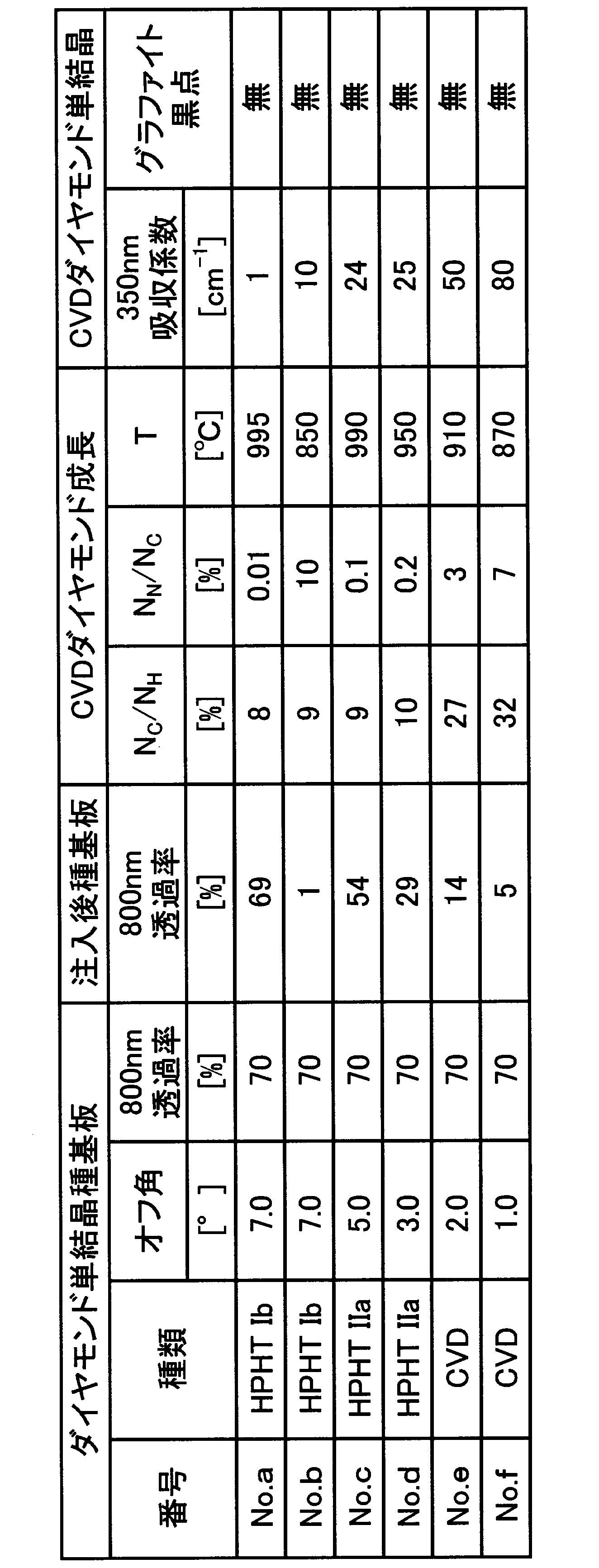
上記で得たダイヤモンド単結晶No.a~No.fをそれぞれ7つずつ用意してイオン注入を行った。そして、このイオン注入後のダイヤモンド単結晶をダイヤモンド単結晶チップとして切削工具のシャンクに接合することで単結晶ダイヤモンド切削工具を作製した。各チップのシャンクへの接合は銀ろう付けにより行った。
ダイヤモンド単結晶チップのイオン注入層除去前後の波長800nmの光の透過率変化(A)は1%~70%、波長350nmの光の吸収係数(B)は1cm-1~80cm-1の範囲のものを表7に示すように準備した。
イオン注入層は、注入イオン種としてリン、注入エネルギーは900keV、注入角度は7°とし、注入ドーズ量は1×1013cm-2~5×1015cm-2の範囲から選択して、前記シャンクに接合する側の主面から注入することにより形成した。注入深さはシャンクに接合する側の主面から0.53μmの位置であった。
すべてのチップのノーズを曲率半径1mm、すくい角0°、逃げ角7°で、輪郭度は50~100nmの範囲に仕上げた。
すなわち、No.3-01~No.3-09の切削工具では、欠けや割れ部分の数と、逃げ面摩耗量との両方の性能において、従来技術の高温高圧合成Ib型ダイヤモンド単結晶で作製した切削工具と同等以上、No.3-10~No.3-42の切削工具では同等より優れた工具性能が得られた。

上記実施例と同様にして作製した全てのダイヤモンド単結晶にイオン注入層を設けなかった以外は、実施例と同様にして、各単結晶ダイヤモンド切削工具を作製した。
実施例と同様にして切削試験を試みたが、差し渡し0.5μm以上の欠け部分あるいは割れ部分の計数結果、7か所より多く、高温高圧合成Ib型ダイヤモンド単結晶で作製した切削工具よりも多かった。
350nmの波長の光の吸収係数が81cm-1及び85cm-1のダイヤモンド単結晶を用いて、両者ともイオン注入加工を施さずに切削工具を作製した。
実施例と同様にして切削試験を試みたが、両方とも切削途中で割れて、切削距離50kmに到達しなかった。
12 ダイヤモンド単結晶種基板の主面
21 単結晶ダイヤモンド工具
22 ダイヤモンド単結晶チップ
23 ホルダ
24 ダイヤモンド単結晶チップの底面
25 ダイヤモンド単結晶チップの背面
31 単結晶ダイヤモンド切削工具
32 ダイヤモンド単結晶チップ
33 ホルダ
34 底面
35 背面
36 イオン注入層
Claims (13)
- 化学気相合成法により合成したダイヤモンド単結晶であって、波長が350nmの光の吸収係数が25cm-1以上、80cm-1以下であるダイヤモンド単結晶。
- 前記吸収係数が30cm-1以上、80cm-1以下である請求項1に記載のダイヤモンド単結晶。
- 気相合成法で作製したダイヤモンド単結晶であって、
350nmの波長の光の吸収係数が異なる二層以上のダイヤモンド単結晶層で構成されており、
一方の主面を含むダイヤモンド単結晶層の350nmの波長の光の吸収係数が25cm-1未満であり、且つ、もう一方の主面を含むダイヤモンド単結晶層の350nmの波長の光の吸収係数が25cm-1以上、80cm-1以下であり、
前記二層以上のダイヤモンド単結晶層のいずれも350nmの波長の光の吸収係数が80cm-1を超えない、ダイヤモンド単結晶。 - 二層以上のダイヤモンド単結晶層を有するダイヤモンド単結晶であって、
一方の主面を含む350nmの波長の光の吸収係数が25cm-1未満のダイヤモンド単結晶層から、もう一方の主面を含む350nmの波長の光の吸収係数が25cm-1以上、80cm-1以下のダイヤモンド単結晶層に向かって、350nmの波長の光の吸収係数が単調増加している、請求項3に記載のダイヤモンド単結晶。 - {100}面からのオフ角が7°以内である面を主面とするダイヤモンド単結晶種基板の主面に炭素以外のイオンを注入して波長が800nmの光の透過率を低下させる工程と、
前記種基板のイオン注入した主面上に化学気相合成法で、気相中の炭素を含有する分子の分子数NCと水素分子数NHとの比NC/NHが10%以上40%以下であり、且つ窒素分子数NNと炭素を含有する分子の分子数NCとの比NN/NCが0.1%以上10%以下であり、且つ種基板温度Tが850℃以上1000℃未満の合成条件でダイヤモンド単結晶をホモエピタキシャル成長させる工程と、
を含む、ダイヤモンド単結晶の製造方法。 - 前記ダイヤモンド単結晶をホモエピタキシャル成長させた成長面にさらに、化学気相合成法で、気相中の炭素を含有する分子の分子数NCと水素分子数NHとの比NC/NHが0%より大きく10%未満か、窒素分子数NNと炭素を含有する分子の分子数NCとの比NN/NCが0.1%未満かのどちらか一方を満たし、且つ種基板温度Tが1000℃未満の合成条件でダイヤモンド単結晶をホモエピタキシャル成長させる工程、
を含む、請求項5に記載のダイヤモンド単結晶の製造方法。 - 前記オフ角が3°以内である請求項5又は請求項6に記載のダイヤモンド単結晶の製造方法。
- 前記種基板と、前記種基板上にホモエピタキシャル成長したダイヤモンド単結晶とを分離する工程を更に含む、請求項5から請求項7のいずれか一項に記載のダイヤモンド単結晶の製造方法。
- 請求項3又は請求項4に記載のダイヤモンド単結晶で刃先を構成する単結晶ダイヤモンド工具であって、
すくい面が、前記ダイヤモンド単結晶の350nmの波長の光の吸収係数が25cm-1未満の主面側で形成されている、単結晶ダイヤモンド工具。 - 工具のシャンクにダイヤモンド単結晶が接合されている単結晶ダイヤモンド工具であって、
前記ダイヤモンド単結晶は、シャンクと接合される側の結晶面からイオン注入加工されたことによるイオン注入層を有する、単結晶ダイヤモンド工具。 - 前記単結晶ダイヤモンド工具は、単結晶ダイヤモンド切削工具である請求項10に記載の単結晶ダイヤモンド工具。
- 前記イオン注入層を有するダイヤモンド単結晶において、イオン注入層に対して垂直方向の波長800nmの光の透過率が、イオン注入層除去前後で10%以上変化する請求項10又は請求項11に記載の単結晶ダイヤモンド工具。
- 前記イオン注入加工される前のダイヤモンド単結晶は、イオン注入層が形成される面に対して垂直方向の波長350nmの光の吸収係数が、25cm-1以上、80cm-1以下である請求項10から請求項12のいずれか一項に記載の単結晶ダイヤモンド工具。
Priority Applications (5)
| Application Number | Priority Date | Filing Date | Title |
|---|---|---|---|
| EP13809060.0A EP2868780B1 (en) | 2012-06-29 | 2013-06-27 | Diamond single crystal and production method thereof, and single crystal diamond tool |
| US14/408,830 US9441312B2 (en) | 2012-06-29 | 2013-06-27 | Diamond single crystal, method for producing the same, and single crystal diamond tool |
| CN201380034864.9A CN104395508B (zh) | 2012-06-29 | 2013-06-27 | 金刚石单晶、其制造方法以及单晶金刚石工具 |
| JP2014522674A JP6315203B2 (ja) | 2012-06-29 | 2013-06-27 | ダイヤモンド単結晶及びその製造方法並びに単結晶ダイヤモンド工具 |
| US15/228,423 US10280531B2 (en) | 2012-06-29 | 2016-08-04 | Diamond single crystal and production method thereof, and single crystal diamond tool |
Applications Claiming Priority (6)
| Application Number | Priority Date | Filing Date | Title |
|---|---|---|---|
| JP2012146444 | 2012-06-29 | ||
| JP2012-146444 | 2012-06-29 | ||
| JP2012152485 | 2012-07-06 | ||
| JP2012-152503 | 2012-07-06 | ||
| JP2012-152485 | 2012-07-06 | ||
| JP2012152503 | 2012-07-06 |
Related Child Applications (2)
| Application Number | Title | Priority Date | Filing Date |
|---|---|---|---|
| US14/408,830 A-371-Of-International US9441312B2 (en) | 2012-06-29 | 2013-06-27 | Diamond single crystal, method for producing the same, and single crystal diamond tool |
| US15/228,423 Continuation US10280531B2 (en) | 2012-06-29 | 2016-08-04 | Diamond single crystal and production method thereof, and single crystal diamond tool |
Publications (1)
| Publication Number | Publication Date |
|---|---|
| WO2014003110A1 true WO2014003110A1 (ja) | 2014-01-03 |
Family
ID=49783247
Family Applications (1)
| Application Number | Title | Priority Date | Filing Date |
|---|---|---|---|
| PCT/JP2013/067632 WO2014003110A1 (ja) | 2012-06-29 | 2013-06-27 | ダイヤモンド単結晶及びその製造方法並びに単結晶ダイヤモンド工具 |
Country Status (5)
| Country | Link |
|---|---|
| US (2) | US9441312B2 (ja) |
| EP (1) | EP2868780B1 (ja) |
| JP (4) | JP6315203B2 (ja) |
| CN (2) | CN106884202B (ja) |
| WO (1) | WO2014003110A1 (ja) |
Cited By (10)
| Publication number | Priority date | Publication date | Assignee | Title |
|---|---|---|---|---|
| WO2016010028A1 (ja) * | 2014-07-15 | 2016-01-21 | 住友電気工業株式会社 | 単結晶ダイヤモンド、単結晶ダイヤモンドの製造方法及び単結晶ダイヤモンドを用いた工具 |
| WO2016035490A1 (ja) * | 2014-09-05 | 2016-03-10 | 住友電工ハードメタル株式会社 | スローアウェイチップ |
| JPWO2016021710A1 (ja) * | 2014-08-08 | 2017-05-25 | 住友電気工業株式会社 | ダイヤモンドの製造方法、ダイヤモンド、ダイヤモンド複合基板、ダイヤモンド接合基板および工具 |
| WO2017090297A1 (ja) * | 2015-11-26 | 2017-06-01 | 住友電工ハードメタル株式会社 | 回転工具 |
| KR20170074973A (ko) * | 2014-10-29 | 2017-06-30 | 스미토모덴키고교가부시키가이샤 | 단결정 다이아몬드 재료, 및 그것을 포함하는 공구, 방사 온도 모니터, 및 적외 광학 부품 |
| US20170241042A1 (en) * | 2015-07-22 | 2017-08-24 | Sumitomo Electric Industries, Ltd. | Single-crystal diamond material, single-crystal diamond chip, and perforated tool |
| WO2019123745A1 (ja) * | 2017-12-20 | 2019-06-27 | 国立研究開発法人産業技術総合研究所 | 単結晶ダイヤモンドおよびそれを用いた半導体素子 |
| JP2019112290A (ja) * | 2017-12-20 | 2019-07-11 | 国立研究開発法人産業技術総合研究所 | 単結晶ダイヤモンドおよびそれを用いた半導体素子 |
| WO2020031871A1 (ja) | 2018-08-06 | 2020-02-13 | 住友電工ハードメタル株式会社 | 旋削工具 |
| US11541464B2 (en) | 2017-03-28 | 2023-01-03 | Sumitomo Electric Hardmetal Corp. | Method for manufacturing diamond single crystal cutting tool using laser pulses |
Families Citing this family (12)
| Publication number | Priority date | Publication date | Assignee | Title |
|---|---|---|---|---|
| EP2868780B1 (en) * | 2012-06-29 | 2020-11-04 | Sumitomo Electric Industries, Ltd. | Diamond single crystal and production method thereof, and single crystal diamond tool |
| US9957640B2 (en) | 2013-04-30 | 2018-05-01 | Sumitomo Electric Industries, Ltd. | Single crystal diamond and diamond tool |
| JP6582597B2 (ja) * | 2015-06-19 | 2019-10-02 | 住友電気工業株式会社 | ダイヤモンド単結晶、工具およびダイヤモンド単結晶の製造方法 |
| EP3330414A4 (en) * | 2015-07-31 | 2019-02-20 | Adamant Namiki Precision Jewel Co., Ltd. | DIAMOND SUBSTRATE AND METHOD FOR PRODUCING THE DIAMOND SUBSTRATE |
| JP6752213B2 (ja) * | 2015-10-19 | 2020-09-09 | 住友電気工業株式会社 | 単結晶ダイヤモンド、これを用いた工具及び単結晶ダイヤモンドの製造方法 |
| CN105364149A (zh) * | 2015-11-18 | 2016-03-02 | 无锡国宏硬质合金模具刃具有限公司 | Mcd单晶高光铣刀 |
| JP7078947B2 (ja) * | 2017-02-06 | 2022-06-01 | 信越化学工業株式会社 | ダイヤモンド製膜用下地基板及びそれを用いたダイヤモンド基板の製造方法 |
| JP7119468B2 (ja) * | 2018-03-20 | 2022-08-17 | 株式会社三洋物産 | 遊技機 |
| JP7119467B2 (ja) * | 2018-03-20 | 2022-08-17 | 株式会社三洋物産 | 遊技機 |
| JP7477130B2 (ja) * | 2018-03-29 | 2024-05-01 | Orbray株式会社 | ダイヤモンド結晶 |
| CN109365845B (zh) * | 2018-11-16 | 2020-07-10 | 深圳市誉和钻石工具有限公司 | 一种光学车刀及其加工工艺 |
| CN109454249B (zh) * | 2018-11-16 | 2021-03-02 | 深圳市誉和钻石工具有限公司 | 一种光学车刀及其切割方法 |
Citations (9)
| Publication number | Priority date | Publication date | Assignee | Title |
|---|---|---|---|---|
| JP2005538018A (ja) * | 2002-09-06 | 2005-12-15 | エレメント シックス リミテッド | 着色されたダイヤモンド |
| JP2007112637A (ja) * | 2005-10-18 | 2007-05-10 | Sumitomo Electric Ind Ltd | ダイヤモンドの加工方法 |
| JP2007191356A (ja) * | 2006-01-19 | 2007-08-02 | Kobe Steel Ltd | 窒素ドープダイヤモンド膜及びその製造方法 |
| JP2008207334A (ja) | 2008-06-09 | 2008-09-11 | Allied Material Corp | 単結晶ダイヤモンドバイト及びその製造方法 |
| JP4344244B2 (ja) | 2001-12-14 | 2009-10-14 | エレメント シックス リミテッド | 着色ダイヤモンド |
| WO2010149777A1 (en) * | 2009-06-26 | 2010-12-29 | Element Six Limited | Method for making fancy orange coloured single crystal cvd diamond and product obtained |
| JP2011519814A (ja) * | 2008-05-05 | 2011-07-14 | カーネギー インスチチューション オブ ワシントン | 超靭性の単結晶ホウ素ドープダイヤモンド |
| JP2012509831A (ja) * | 2008-11-25 | 2012-04-26 | カーネギー インスチチューション オブ ワシントン | 急速成長速度における単結晶cvdダイヤモンドの製造 |
| JP2013035732A (ja) * | 2011-08-10 | 2013-02-21 | Sumitomo Electric Ind Ltd | 導電層付き単結晶ダイヤモンドおよびそれを用いた工具 |
Family Cites Families (16)
| Publication number | Priority date | Publication date | Assignee | Title |
|---|---|---|---|---|
| JPH02237703A (ja) * | 1989-03-10 | 1990-09-20 | Mitsubishi Electric Corp | ダイヤモンドバイトおよびこのバイトを用いた切削装置 |
| DE69112465T2 (de) * | 1990-03-30 | 1996-03-28 | Sumitomo Electric Industries | Polykristallines Diamantwerkzeug und Verfahren für seine Herstellung. |
| JP2591865B2 (ja) * | 1990-03-30 | 1997-03-19 | 住友電気工業株式会社 | 多結晶ダイヤモンド工具及びその製造方法 |
| JPH05197309A (ja) | 1992-01-20 | 1993-08-06 | Konica Corp | 画像形成装置の定着器 |
| US5439492A (en) * | 1992-06-11 | 1995-08-08 | General Electric Company | Fine grain diamond workpieces |
| JPH08197309A (ja) * | 1995-01-19 | 1996-08-06 | Fanuc Ltd | イオン注入したダイヤモンド切削工具 |
| AU2001255388A1 (en) * | 2000-04-14 | 2001-10-30 | Technology International, Inc. | Diamonds and diamond cutters having improved durability |
| JP2004022821A (ja) | 2002-06-17 | 2004-01-22 | Shibaura Mechatronics Corp | ドライエッチング方法および装置 |
| GB0220772D0 (en) * | 2002-09-06 | 2002-10-16 | Diamanx Products Ltd | Coloured diamond |
| BRPI0515347A (pt) * | 2004-09-10 | 2008-07-22 | Carnegie Inst Of Washington | diamante de cristal único cvd ultra-resistente e crescimento tridimensional do mesmo |
| GB0512728D0 (en) * | 2005-06-22 | 2005-07-27 | Element Six Ltd | High colour diamond |
| JP4873467B2 (ja) * | 2006-07-27 | 2012-02-08 | 独立行政法人産業技術総合研究所 | オフ角を有する単結晶基板の製造方法 |
| JP5067571B2 (ja) * | 2008-07-16 | 2012-11-07 | 住友電気工業株式会社 | ダイヤモンド単結晶基板とその製造方法 |
| JP4849691B2 (ja) * | 2008-12-25 | 2012-01-11 | 独立行政法人産業技術総合研究所 | 大面積ダイヤモンド結晶基板及びその製造方法 |
| JP5382742B2 (ja) * | 2011-10-20 | 2014-01-08 | 独立行政法人産業技術総合研究所 | オフ角を有する単結晶基板の製造方法 |
| EP2868780B1 (en) * | 2012-06-29 | 2020-11-04 | Sumitomo Electric Industries, Ltd. | Diamond single crystal and production method thereof, and single crystal diamond tool |
-
2013
- 2013-06-27 EP EP13809060.0A patent/EP2868780B1/en active Active
- 2013-06-27 CN CN201610991581.9A patent/CN106884202B/zh active Active
- 2013-06-27 US US14/408,830 patent/US9441312B2/en active Active
- 2013-06-27 CN CN201380034864.9A patent/CN104395508B/zh active Active
- 2013-06-27 WO PCT/JP2013/067632 patent/WO2014003110A1/ja active Application Filing
- 2013-06-27 JP JP2014522674A patent/JP6315203B2/ja active Active
-
2016
- 2016-08-04 US US15/228,423 patent/US10280531B2/en active Active
-
2017
- 2017-09-28 JP JP2017188357A patent/JP6409930B2/ja active Active
- 2017-09-28 JP JP2017188360A patent/JP6536847B2/ja active Active
-
2019
- 2019-01-16 JP JP2019005124A patent/JP6665952B2/ja active Active
Patent Citations (10)
| Publication number | Priority date | Publication date | Assignee | Title |
|---|---|---|---|---|
| JP4344244B2 (ja) | 2001-12-14 | 2009-10-14 | エレメント シックス リミテッド | 着色ダイヤモンド |
| JP2005538018A (ja) * | 2002-09-06 | 2005-12-15 | エレメント シックス リミテッド | 着色されたダイヤモンド |
| JP2007112637A (ja) * | 2005-10-18 | 2007-05-10 | Sumitomo Electric Ind Ltd | ダイヤモンドの加工方法 |
| JP2007191356A (ja) * | 2006-01-19 | 2007-08-02 | Kobe Steel Ltd | 窒素ドープダイヤモンド膜及びその製造方法 |
| JP2011519814A (ja) * | 2008-05-05 | 2011-07-14 | カーネギー インスチチューション オブ ワシントン | 超靭性の単結晶ホウ素ドープダイヤモンド |
| JP2008207334A (ja) | 2008-06-09 | 2008-09-11 | Allied Material Corp | 単結晶ダイヤモンドバイト及びその製造方法 |
| JP2012509831A (ja) * | 2008-11-25 | 2012-04-26 | カーネギー インスチチューション オブ ワシントン | 急速成長速度における単結晶cvdダイヤモンドの製造 |
| WO2010149777A1 (en) * | 2009-06-26 | 2010-12-29 | Element Six Limited | Method for making fancy orange coloured single crystal cvd diamond and product obtained |
| WO2010149775A1 (en) * | 2009-06-26 | 2010-12-29 | Element Six Limited | Method for treating single crystal cvd diamond and product obtained |
| JP2013035732A (ja) * | 2011-08-10 | 2013-02-21 | Sumitomo Electric Ind Ltd | 導電層付き単結晶ダイヤモンドおよびそれを用いた工具 |
Non-Patent Citations (2)
| Title |
|---|
| RIZWAN U. A. KHAN ET AL.: "Color alterations in CVD synthetic diamond with heat and UV exposure: implications for color grading and identification", GEM & GEMOLOGY, SPRING, 2010, pages 18 - 26 |
| See also references of EP2868780A4 * |
Cited By (35)
| Publication number | Priority date | Publication date | Assignee | Title |
|---|---|---|---|---|
| CN106460226A (zh) * | 2014-07-15 | 2017-02-22 | 住友电气工业株式会社 | 单晶金刚石、制造单晶金刚石的方法和包含单晶金刚石的工具 |
| JPWO2016010028A1 (ja) * | 2014-07-15 | 2017-04-27 | 住友電気工業株式会社 | 単結晶ダイヤモンド、単結晶ダイヤモンドの製造方法及び単結晶ダイヤモンドを用いた工具 |
| US20170130362A1 (en) * | 2014-07-15 | 2017-05-11 | Sumitomo Electric Industries, Ltd. | Single crystal diamond, method for manufacturing single crystal diamond, and tool containing single crystal diamond |
| US10316430B2 (en) | 2014-07-15 | 2019-06-11 | Sumitomo Electric Industries, Ltd. | Single crystal diamond, method for manufacturing single crystal diamond, and tool containing single crystal diamond |
| WO2016010028A1 (ja) * | 2014-07-15 | 2016-01-21 | 住友電気工業株式会社 | 単結晶ダイヤモンド、単結晶ダイヤモンドの製造方法及び単結晶ダイヤモンドを用いた工具 |
| US20170233889A1 (en) * | 2014-08-08 | 2017-08-17 | Sumitomo Electric Industries, Ltd. | Method of manufacturing diamond, diamond, diamond composite substrate, diamond joined substrate, and tool |
| US11371139B2 (en) | 2014-08-08 | 2022-06-28 | Sumitomo Electric Industries, Ltd. | Method of manufacturing diamond, diamond, diamond composite substrate, diamond joined substrate, and tool |
| US10584428B2 (en) | 2014-08-08 | 2020-03-10 | Sumitomo Electric Industries, Ltd. | Method of manufacturing diamond, diamond, diamond composite substrate, diamond joined substrate, and tool |
| JPWO2016021710A1 (ja) * | 2014-08-08 | 2017-05-25 | 住友電気工業株式会社 | ダイヤモンドの製造方法、ダイヤモンド、ダイヤモンド複合基板、ダイヤモンド接合基板および工具 |
| JPWO2016035490A1 (ja) * | 2014-09-05 | 2017-06-22 | 住友電工ハードメタル株式会社 | スローアウェイチップ |
| CN105682833A (zh) * | 2014-09-05 | 2016-06-15 | 住友电工硬质合金株式会社 | 一次性刀具 |
| US10286455B2 (en) | 2014-09-05 | 2019-05-14 | Sumitomo Electric Hardmetal Corp. | Throw-away tip |
| WO2016035490A1 (ja) * | 2014-09-05 | 2016-03-10 | 住友電工ハードメタル株式会社 | スローアウェイチップ |
| US10697088B2 (en) | 2014-10-29 | 2020-06-30 | Sumitomo Electric Industries, Ltd. | Single-crystal diamond material, and tool, radiation temperature monitor, and infrared optical component including said diamond material |
| KR20170074973A (ko) * | 2014-10-29 | 2017-06-30 | 스미토모덴키고교가부시키가이샤 | 단결정 다이아몬드 재료, 및 그것을 포함하는 공구, 방사 온도 모니터, 및 적외 광학 부품 |
| CN107109690B (zh) * | 2014-10-29 | 2019-08-20 | 住友电气工业株式会社 | 单晶金刚石材料和包括所述金刚石材料的工具、辐射温度监测器和红外光学组件 |
| CN107109690A (zh) * | 2014-10-29 | 2017-08-29 | 住友电气工业株式会社 | 单晶金刚石材料和包括所述金刚石材料的工具、辐射温度监测器和红外光学组件 |
| EP3214208A4 (en) * | 2014-10-29 | 2018-06-27 | Sumitomo Electric Industries, Ltd. | Single-crystal diamond material, and tool, radiation temperature monitor, and infrared optical component including said diamond material |
| KR102475053B1 (ko) * | 2014-10-29 | 2022-12-06 | 스미토모덴키고교가부시키가이샤 | 단결정 다이아몬드 재료, 및 그것을 포함하는 공구, 방사 온도 모니터, 및 적외 광학 부품 |
| US10287708B2 (en) * | 2015-07-22 | 2019-05-14 | Sumitomo Electric Industries, Ltd. | Single-crystal diamond material, single-crystal diamond chip, and perforated tool |
| US10774442B2 (en) | 2015-07-22 | 2020-09-15 | Sumitomo Electric Industries, Ltd. | Single-crystal diamond material, single-crystal diamond chip, and perforated tool |
| CN107109691A (zh) * | 2015-07-22 | 2017-08-29 | 住友电气工业株式会社 | 单晶金刚石材料、单晶金刚石芯片和穿孔工具 |
| US20170241042A1 (en) * | 2015-07-22 | 2017-08-24 | Sumitomo Electric Industries, Ltd. | Single-crystal diamond material, single-crystal diamond chip, and perforated tool |
| US10493536B2 (en) | 2015-11-26 | 2019-12-03 | Sumitomo Electric Hardmetal Corp. | Rotary tool |
| WO2017090297A1 (ja) * | 2015-11-26 | 2017-06-01 | 住友電工ハードメタル株式会社 | 回転工具 |
| US20180318939A1 (en) * | 2015-11-26 | 2018-11-08 | Sumitomo Electric Hardmetal Corp. | Rotary tool |
| US11541464B2 (en) | 2017-03-28 | 2023-01-03 | Sumitomo Electric Hardmetal Corp. | Method for manufacturing diamond single crystal cutting tool using laser pulses |
| JP2019112290A (ja) * | 2017-12-20 | 2019-07-11 | 国立研究開発法人産業技術総合研究所 | 単結晶ダイヤモンドおよびそれを用いた半導体素子 |
| JP2020128328A (ja) * | 2017-12-20 | 2020-08-27 | 国立研究開発法人産業技術総合研究所 | 単結晶ダイヤモンドおよびそれを用いた半導体素子 |
| WO2019123745A1 (ja) * | 2017-12-20 | 2019-06-27 | 国立研究開発法人産業技術総合研究所 | 単結晶ダイヤモンドおよびそれを用いた半導体素子 |
| US11355591B2 (en) | 2017-12-20 | 2022-06-07 | National Institute Of Advanced Industrial Science And Technology | Single crystal diamond and semiconductor element using same |
| WO2020031871A1 (ja) | 2018-08-06 | 2020-02-13 | 住友電工ハードメタル株式会社 | 旋削工具 |
| CN112533713A (zh) * | 2018-08-06 | 2021-03-19 | 住友电工硬质合金株式会社 | 车削工具 |
| US11938547B2 (en) | 2018-08-06 | 2024-03-26 | Sumitomo Electric Hardmetal Corp. | Turning tool |
| CN112533713B (zh) * | 2018-08-06 | 2024-04-05 | 住友电工硬质合金株式会社 | 车削工具 |
Also Published As
| Publication number | Publication date |
|---|---|
| EP2868780B1 (en) | 2020-11-04 |
| CN106884202A (zh) | 2017-06-23 |
| JP6536847B2 (ja) | 2019-07-03 |
| JP2018039724A (ja) | 2018-03-15 |
| US20160340801A1 (en) | 2016-11-24 |
| JP6665952B2 (ja) | 2020-03-13 |
| CN106884202B (zh) | 2019-12-03 |
| JPWO2014003110A1 (ja) | 2016-06-02 |
| EP2868780A4 (en) | 2016-05-18 |
| JP6409930B2 (ja) | 2018-10-24 |
| US10280531B2 (en) | 2019-05-07 |
| JP2018052807A (ja) | 2018-04-05 |
| US20150176155A1 (en) | 2015-06-25 |
| US9441312B2 (en) | 2016-09-13 |
| EP2868780A1 (en) | 2015-05-06 |
| JP2019081699A (ja) | 2019-05-30 |
| JP6315203B2 (ja) | 2018-04-25 |
| CN104395508A (zh) | 2015-03-04 |
| CN104395508B (zh) | 2016-12-21 |
Similar Documents
| Publication | Publication Date | Title |
|---|---|---|
| JP6409930B2 (ja) | Cvdダイヤモンド単結晶 | |
| TWI650450B (zh) | 高度成雙晶的定向多晶鑽石膜以及製造彼之方法 | |
| JP6752143B2 (ja) | 合成単結晶ダイヤモンド、合成単結晶ダイヤモンドの製造方法及び合成単結晶ダイヤモンドを用いた工具 | |
| EP2985368B1 (en) | Single crystal diamond and diamond tool | |
| CN107923067B (zh) | 单晶金刚石、使用单晶金刚石的工具以及单晶金刚石的制造方法 | |
| US11684981B2 (en) | Ultra-fine nanocrystalline diamond precision cutting tool and manufacturing method therefor | |
| JP2018162212A (ja) | 単結晶ダイヤモンドおよびダイヤモンド工具 | |
| JP7232186B2 (ja) | 単結晶ダイヤモンドおよびその製造方法 | |
| TWI852913B (zh) | 單結晶鑽石 | |
| JP2014214076A (ja) | ダイヤモンド複合体、単結晶ダイヤモンドおよびこれらの製造方法、ならびにダイヤモンド工具 | |
| WO2021065258A1 (ja) | ダイヤモンド棒状体、ダイヤモンド工具およびカンチレバー |
Legal Events
| Date | Code | Title | Description |
|---|---|---|---|
| 121 | Ep: the epo has been informed by wipo that ep was designated in this application |
Ref document number: 13809060 Country of ref document: EP Kind code of ref document: A1 |
|
| ENP | Entry into the national phase |
Ref document number: 2014522674 Country of ref document: JP Kind code of ref document: A |
|
| WWE | Wipo information: entry into national phase |
Ref document number: 2013809060 Country of ref document: EP |
|
| WWE | Wipo information: entry into national phase |
Ref document number: 14408830 Country of ref document: US |
|
| NENP | Non-entry into the national phase |
Ref country code: DE |