WO2013157516A1 - 導電性ペースト、積層セラミック電子部品、および該積層セラミック電子部品の製造方法 - Google Patents
導電性ペースト、積層セラミック電子部品、および該積層セラミック電子部品の製造方法 Download PDFInfo
- Publication number
- WO2013157516A1 WO2013157516A1 PCT/JP2013/061172 JP2013061172W WO2013157516A1 WO 2013157516 A1 WO2013157516 A1 WO 2013157516A1 JP 2013061172 W JP2013061172 W JP 2013061172W WO 2013157516 A1 WO2013157516 A1 WO 2013157516A1
- Authority
- WO
- WIPO (PCT)
- Prior art keywords
- conductive paste
- ceramic
- powder
- electronic component
- internal electrode
- Prior art date
- Legal status (The legal status is an assumption and is not a legal conclusion. Google has not performed a legal analysis and makes no representation as to the accuracy of the status listed.)
- Ceased
Links
Images
Classifications
-
- H—ELECTRICITY
- H10—SEMICONDUCTOR DEVICES; ELECTRIC SOLID-STATE DEVICES NOT OTHERWISE PROVIDED FOR
- H10N—ELECTRIC SOLID-STATE DEVICES NOT OTHERWISE PROVIDED FOR
- H10N60/00—Superconducting devices
- H10N60/01—Manufacture or treatment
-
- C—CHEMISTRY; METALLURGY
- C09—DYES; PAINTS; POLISHES; NATURAL RESINS; ADHESIVES; COMPOSITIONS NOT OTHERWISE PROVIDED FOR; APPLICATIONS OF MATERIALS NOT OTHERWISE PROVIDED FOR
- C09D—COATING COMPOSITIONS, e.g. PAINTS, VARNISHES OR LACQUERS; FILLING PASTES; CHEMICAL PAINT OR INK REMOVERS; INKS; CORRECTING FLUIDS; WOODSTAINS; PASTES OR SOLIDS FOR COLOURING OR PRINTING; USE OF MATERIALS THEREFOR
- C09D133/00—Coating compositions based on homopolymers or copolymers of compounds having one or more unsaturated aliphatic radicals, each having only one carbon-to-carbon double bond, and at least one being terminated by only one carboxyl radical, or of salts, anhydrides, esters, amides, imides, or nitriles thereof; Coating compositions based on derivatives of such polymers
- C09D133/04—Homopolymers or copolymers of esters
- C09D133/06—Homopolymers or copolymers of esters of esters containing only carbon, hydrogen and oxygen, the oxygen atom being present only as part of the carboxyl radical
- C09D133/08—Homopolymers or copolymers of acrylic acid esters
-
- C—CHEMISTRY; METALLURGY
- C09—DYES; PAINTS; POLISHES; NATURAL RESINS; ADHESIVES; COMPOSITIONS NOT OTHERWISE PROVIDED FOR; APPLICATIONS OF MATERIALS NOT OTHERWISE PROVIDED FOR
- C09D—COATING COMPOSITIONS, e.g. PAINTS, VARNISHES OR LACQUERS; FILLING PASTES; CHEMICAL PAINT OR INK REMOVERS; INKS; CORRECTING FLUIDS; WOODSTAINS; PASTES OR SOLIDS FOR COLOURING OR PRINTING; USE OF MATERIALS THEREFOR
- C09D5/00—Coating compositions, e.g. paints, varnishes or lacquers, characterised by their physical nature or the effects produced; Filling pastes
- C09D5/24—Electrically-conducting paints
-
- H—ELECTRICITY
- H01—ELECTRIC ELEMENTS
- H01B—CABLES; CONDUCTORS; INSULATORS; SELECTION OF MATERIALS FOR THEIR CONDUCTIVE, INSULATING OR DIELECTRIC PROPERTIES
- H01B1/00—Conductors or conductive bodies characterised by the conductive materials; Selection of materials as conductors
- H01B1/20—Conductive material dispersed in non-conductive organic material
- H01B1/22—Conductive material dispersed in non-conductive organic material the conductive material comprising metals or alloys
-
- H—ELECTRICITY
- H01—ELECTRIC ELEMENTS
- H01G—CAPACITORS; CAPACITORS, RECTIFIERS, DETECTORS, SWITCHING DEVICES, LIGHT-SENSITIVE OR TEMPERATURE-SENSITIVE DEVICES OF THE ELECTROLYTIC TYPE
- H01G4/00—Fixed capacitors; Processes of their manufacture
- H01G4/002—Details
- H01G4/005—Electrodes
- H01G4/008—Selection of materials
- H01G4/0085—Fried electrodes
-
- H—ELECTRICITY
- H01—ELECTRIC ELEMENTS
- H01G—CAPACITORS; CAPACITORS, RECTIFIERS, DETECTORS, SWITCHING DEVICES, LIGHT-SENSITIVE OR TEMPERATURE-SENSITIVE DEVICES OF THE ELECTROLYTIC TYPE
- H01G4/00—Fixed capacitors; Processes of their manufacture
- H01G4/002—Details
- H01G4/018—Dielectrics
- H01G4/06—Solid dielectrics
- H01G4/08—Inorganic dielectrics
- H01G4/12—Ceramic dielectrics
-
- H—ELECTRICITY
- H01—ELECTRIC ELEMENTS
- H01G—CAPACITORS; CAPACITORS, RECTIFIERS, DETECTORS, SWITCHING DEVICES, LIGHT-SENSITIVE OR TEMPERATURE-SENSITIVE DEVICES OF THE ELECTROLYTIC TYPE
- H01G4/00—Fixed capacitors; Processes of their manufacture
- H01G4/002—Details
- H01G4/228—Terminals
- H01G4/232—Terminals electrically connecting two or more layers of a stacked or rolled capacitor
-
- H—ELECTRICITY
- H01—ELECTRIC ELEMENTS
- H01G—CAPACITORS; CAPACITORS, RECTIFIERS, DETECTORS, SWITCHING DEVICES, LIGHT-SENSITIVE OR TEMPERATURE-SENSITIVE DEVICES OF THE ELECTROLYTIC TYPE
- H01G4/00—Fixed capacitors; Processes of their manufacture
- H01G4/30—Stacked capacitors
Definitions
- the present invention relates to a conductive paste and a multilayer ceramic electronic component using the same, and more specifically, a conductive paste suitable for use in manufacturing a multilayer ceramic electronic component, a multilayer ceramic electronic component manufactured using the same, and The present invention relates to a method for manufacturing the multilayer ceramic electronic component.
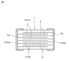
- One typical ceramic electronic component is, for example, a multilayer ceramic capacitor having a structure as shown in FIG. As shown in FIG. 1, this multilayer ceramic capacitor is provided on both end faces 4a and 4b of a multilayer ceramic capacitor element 1 in which a plurality of internal electrodes 2 (2a and 2b) are laminated via a ceramic layer 3 which is a dielectric layer.
- the external electrode 5 (5a, 5b) is disposed so as to be electrically connected to the internal electrode 2 (2a, 2b).
- such a multilayer ceramic capacitor is usually (a) a green sheet formed with an internal electrode pattern by printing on the surface thereof a conductive paste obtained by kneading an organic vehicle containing an organic binder and a solvent and a conductive metal powder, and the internal electrode pattern A step of preparing a green sheet in which no is formed, (b) a step of laminating a green sheet on which an internal electrode pattern is formed and a green sheet on which no internal electrode pattern is formed in a predetermined order to form a laminate; (c) a step of dividing the multilayer body formed in (b) above into individual multilayer ceramic capacitor elements (unfired multilayer ceramic capacitor elements); (d) a step of firing an unfired multilayer ceramic capacitor element after heat-treating at a predetermined temperature to remove the binder; (e) Manufactured through a series of processes such as a process of forming external electrodes on the fired multilayer ceramic capacitor element.
- the conductive paste used to form the internal electrode also has good printability, high coating film smoothness, and a conductive material capable of forming a thick film electrode (conductor film) with low residue and high filling properties.
- a conductive paste that is, a conductive paste that can realize denseness, high reliability, thin layer high coverage, and the like in an internal electrode formed using the paste.
- the conductive paste suitable for forming the internal electrode (conductor film) with high surface smoothness and high coverage can be provided, and as an embodiment An example of a conductive paste using ethyl cellulose as a binder resin constituting an organic vehicle is shown.
- conductive paste As another conductive paste, conductive powder, a binder resin and an additive are contained, and the binder resin is an acrylic resin having a carboxyl group having an acid value of 3 to 15 mgKOH / g and a weight average molecular weight Mw of 50,000 to 150,000.
- a conductive paste for gravure printing, which is a resin, has been proposed (see Patent Document 2).
- the present invention solves the above-mentioned problems, has good printability, high filling property of conductive metal powder in the conductive paste film after printing, excellent smoothness and continuity after firing, and residue Conductive paste capable of forming a small number of conductor films (internal electrodes), a highly reliable multilayer ceramic electronic component using the same, and having a high coverage internal electrode with few structural defects, and its manufacture It aims to provide a method.
- the invention of the conductive paste of the present invention is A conductive paste containing a conductive metal powder, an organic solvent, and an acrylic resin,
- the conductive metal powder has an average particle size in the range of 50 to 200 nm;
- the acrylic resin has a weight average molecular weight in the range of 160000 to 1000000, and
- the acrylic resin content is in a range of 20 to 200% by volume with respect to 100% by volume of the metal powder.
- the average particle diameter of the said conductive metal powder calculates a particle diameter by image analysis from the SEM image of a powder, calculates
- the weight average molecular weight of the acrylic resin is a value measured by gel permeation chromatography.
- the average particle size of the conductive metal powder is set in the range of 50 to 200 nm because when the average particle size of the conductive metal powder is less than 50 nm, the cohesiveness increases and the conductive particle powder is good. Dispersion is not only difficult, but also high sinterability makes it impossible to obtain a sintered film with high continuity due to spheroidization, and if it exceeds 200 nm, the surface roughness of the coating becomes rough and ceramic This is because the reliability is lowered in the region where the layer is thin.
- the acrylic resin content is in the range of 20 to 200% by volume with respect to 100% by volume of the metal powder. If the addition amount of the acrylic resin is less than 20% by volume, the conductive paste is stable. Rheology is not obtained, printability is reduced, and if it exceeds 200% by volume, the amount of acrylic resin in the coating film is excessively increased, the filling property of the metal powder is reduced, and a continuous sintered film is obtained. Because it becomes difficult.
- the weight average molecular weight of the acrylic resin is set in the range of 160000 to 1000000 because when the molecular weight of the acrylic resin is less than 160000, the structural viscosity is increased due to the use of the fine powder as the conductive metal powder.
- the printability cannot be obtained and the value exceeds 1000000, the fluidity of the conductive paste is lowered, and good printability cannot be obtained.
- the electrically conductive paste of this invention contains a ceramic powder further.
- ceramic powder When ceramic powder is included, conductive paste is applied to a ceramic substrate (ceramic green sheet, etc.) to form an electrode pattern, and when this is fired, sintering of the conductive metal powder is suppressed and fired. It becomes possible to obtain a conductor film (electrode) having a thinner film thickness, a dense film, and high continuity.
- the conductive metal powder is preferably at least one powder selected from the group consisting of copper, nickel, silver, and palladium, or an alloy powder containing at least one selected from the above group.
- a conductive paste is applied to a ceramic substrate (ceramic green sheet, etc.) to form an electrode pattern, which is then fired. It is possible to prevent the material from diffusing into the ceramic element, and to obtain a conductive film (electrode) having a thin film thickness and high continuity, which can make the present invention more effective.
- the average particle size of the ceramic powder is preferably in the range of 5 to 100 nm.
- the average particle size of the ceramic powder is the value computed from the specific surface area by BET method.
- the ceramic powder it is preferable to use a composite oxide powder having a perovskite structure represented by the general formula: ABO 3 .
- a powder of a composite oxide having a perovskite structure represented by the general formula: ABO 3 as the ceramic powder, for example, when the conductive paste of the present invention is used for forming an internal electrode of a multilayer ceramic capacitor, It becomes possible to use a conductive paste containing the same kind of ceramic powder as the ceramic material constituting the ceramic layer that functions as the dielectric layer.
- the internal electrode pattern is fired to form the internal electrode, It is possible to suppress an undesirable influence on the characteristics and, consequently, the multilayer ceramic capacitor element.
- the internal electrode forming paste of the multilayer ceramic electronic component of the present invention comprises a plurality of ceramic layers and a plurality of internal electrodes, and the multilayer ceramic electronic has a structure in which the internal electrodes are stacked via the ceramic layers. It is characterized in that it is used for forming the internal electrode when manufacturing a component.
- the multilayer ceramic electronic component of the present invention is A multilayer ceramic electronic component comprising a plurality of ceramic layers and a plurality of internal electrodes, wherein the internal electrodes have a structure laminated via the ceramic layers,
- the internal electrode is formed using the above-described conductive paste of the present invention.
- the method for manufacturing the multilayer ceramic electronic component of the present invention includes: A method for manufacturing a multilayer ceramic electronic component comprising a plurality of ceramic layers and a plurality of internal electrodes, wherein the internal electrodes are stacked via the ceramic layers, A ceramic green sheet that becomes the ceramic layer after firing and an internal electrode pattern that is formed by printing the conductive paste of the present invention described above and becomes the internal electrode after firing, the internal electrode pattern being the ceramic green Forming an unfired laminate having a structure laminated through sheets; And firing the green laminate.
- the conductive paste of the present invention includes a conductive metal powder, an organic solvent, and an acrylic resin, an average particle size of the conductive metal powder of 50 to 200 nm, and a weight average molecular weight of the acrylic resin of 160000 to 1000000.
- the content of the acrylic resin is in the range of 20 to 200% by volume with respect to 100% by volume of the metal powder, the printability is good and the conductive metal powder in the conductive paste film formed by printing It is possible to provide a conductive paste that can form a conductive film (internal electrode) that has a high filling property, is excellent in smoothness and continuity by firing, and has few residues.
- the laminate in which the internal electrode is formed using the conductive paste of the present invention can achieve improvement in characteristics by including the internal electrode with high reliability, low defect rate, and thin layer and high coverage.
- the multilayer ceramic electronic component of the present invention provided with the internal electrode formed using the above-described conductive paste of the present invention is formed of a conductive film in which the internal electrode is excellent in smoothness and continuity and has little residue. Therefore, it is possible to provide a multilayer ceramic electronic component having high characteristics and having desired characteristics.
- an internal electrode pattern is formed on a ceramic green sheet using the above-described conductive paste of the present invention, and this is fired to form an internal electrode. Therefore, it is possible to form an internal electrode having a desired shape and dimensions, excellent smoothness and continuity, and with less residue, and a highly reliable multilayer ceramic electronic component having desired characteristics. It can be manufactured reliably.
- Conductive metal powder As shown in Table 1, as the conductive metal powder, a) Copper (Cu) having an average particle size of 40 nm, 50 nm, 150 nm, 180 nm, 200 nm, and 210 nm, b) Nickel (Ni) having an average particle diameter of 200 nm, c) Silver (Ag) having an average particle size of 150 nm, d) Palladium (Pd) with an average particle size of 150 nm Prepared.
- the range of the average particle diameter of the conductive metal powder in the present invention is in the range of 50 to 200 nm.
- the conductive metal powder was blended in such a ratio that the content in the conductive paste occupies 6.5% by volume in any of the samples in Table 1.
- the average particle diameter of the conductive metal powder is obtained by calculating the particle diameter from the SEM image of the powder by image analysis and obtaining the average value of 100 particles to obtain the average particle diameter.
- Ceramic powder As ceramic powder, a) Calcium zirconate (CaZrO 3 ) powder having an average particle size of 5 nm, 50 nm, and 100 nm, b) Barium titanate (BaTiO 3 ) powder having an average particle diameter of 50 nm was prepared. In addition, the average particle diameter of said ceramic powder is the value calculated
- CaZrO 3 Calcium zirconate
- BaTiO 3 Barium titanate
- Acrylic resin As acrylic resins, six kinds of acrylic resins having different weight average molecular weights in the range of 150,000 to 1200000 (molecular weights of 150,000, 160000, 200000, 800,000, 1000000, 1200000) were prepared. However, the range of the weight average molecular weight of the acrylic resin in the present invention is in the range of 1600000 to 1000000. The weight average molecular weight of the acrylic resin is a value measured by gel permeation chromatography.
- Solvent Dihydroterpineol was prepared as a solvent.
- dihydroterpineol was used as a solvent.
- solvents diethyl ether, dipropyl ether, diisopropyl ether, anisole, phenetole, benzyl ethyl ether, diphenyl ether, dibenzyl ether, dioxane, tetrahydrofuran, ethylene glycol dimethyl ether, ethylene glycol diethyl ether, acetal, acetone, methyl ethyl ketone, methyl Propyl ketone, methyl butyl ketone, methyl pentyl ketone, diethyl ketone, methyl isobutyl ketone, diisobutyl ketone, acetonyl acetone, isophorone, cyclohexanone, methyl cyclohexanone, acetophenone, cam
- each raw material was blended within the following range, premixed with a planetary mixer, and then dispersed with a three-roll mill to prepare a conductive paste.
- Conductive metal powder copper, nickel, silver, or palladium powder
- Ceramic powder Ceramic powder (CaZrO 3 or BaTiO 3 ): 0 or 1% by volume
- Solvent dihydroterpineol: 79.0 to 92.2% by volume
- Sample No. 1 (conductive paste) in Table 1 is a sample according to an example of the present invention, 6.5% by volume of copper powder having an average particle diameter of 200 nm, 84.5% by volume of dihydroterpineol, and a weight average molecular weight of 160000. This is a sample in which 9.0% by volume of acrylic resin is blended, and the ceramic powder is not blended.
- Sample No. 2 (conductive paste) in Table 1 is a sample according to an example of the present invention, 6.5% by volume of copper powder having an average particle diameter of 180 nm, 83.5% by volume of dihydroterpineol, and a weight average molecular weight of 200,000.
- This sample is a sample in which 9.0% by volume of acrylic resin is blended, and as a ceramic powder, calcium zirconate having an average particle size of 100 nm is blended in a proportion of 1% by volume.
- Samples Nos. 3 to 8 (conductive paste) in Table 1 are samples according to the examples of the present invention.
- the conductive metal powder species and their particle sizes, the ceramic powder species and their particle sizes, and the weight average of acrylic resin The sample was prepared with the molecular weight and the amount added as shown in Table 1.
- Samples Nos. 9 to 14 (conductive paste) in Table 1 are comparative examples that do not have the requirements of the present invention, and are conductive metal powder species and their particle sizes, ceramic powder species and their particle sizes.
- Table 1 shows combinations of weight average molecular weight of acrylic resin and addition amount thereof as shown in Table 1.
- multilayer ceramic electronic components multilayer ceramic capacitors
- conductive pastes of the above sample numbers 1 to 14 multilayer ceramic electronic components (multilayer ceramic capacitors) were produced by the method described below.
- a ball mill is prepared by adding a polyvinyl butyral binder and an organic solvent such as ethanol to a reduction-resistant dielectric ceramic raw material powder mainly composed of calcium zirconate having an average particle size of 100 to 500 nm. To obtain a ceramic slurry. Then, the ceramic slurry was formed into a sheet shape by a doctor blade method so that the thickness after firing was 2 ⁇ m, and a ceramic green sheet was produced.
- the conductive paste film internal electrode pattern
- print quality such as blurring and blurring was determined from the shape of the printed pattern when the conductive paste was printed on the ceramic green sheet, and the printability of the conductive paste was evaluated.
- printability of the conductive paste specifically, those with no blurring and blurring were evaluated as having good printability ( ⁇ ), and those with blurring and blurring were poor in printability ( ⁇ ). It was evaluated that.
- the evaluation results of the printability of the conductive paste are also shown in Table 1.
- the conductor filling property (metal filling property) of the coating film was evaluated from the ratio of the conductor coating thickness measured using a fluorescent X-ray film thickness meter and the actual physical thickness of the coating film.
- the conductor filling property specifically, the conductor coating thickness occupying 31% or more of the physical thickness is evaluated as having good conductor filling property ( ⁇ ), and the conductor filling thickness is less than 31%.
- the conductor filling property was evaluated as poor (x).
- the evaluation results of the conductor filling properties are also shown in Table 1.
- a plurality of ceramic green sheets including a ceramic green sheet on which a conductive paste film (internal electrode pattern) was formed were laminated in a predetermined order and integrated by hot pressing to produce a hot press block. Thereafter, this hot press block was cut into a predetermined size to obtain a raw laminate (unfired laminate).
- this unfired laminate is heated to 200 to 300 ° C. in a nitrogen atmosphere to decompose the binder, and then in a reducing atmosphere comprising H 2 —N 2 —H 2 O gas. Were fired at a maximum firing temperature of 1200 to 1300 ° C. to obtain a sintered body (sintered laminate).
- the multilayer ceramic capacitor manufactured in this embodiment has both ends of a multilayer ceramic capacitor element 1 in which a plurality of internal electrodes 2 (2a, 2b) are stacked via a ceramic layer 3 that is a dielectric layer.
- the external electrodes 5 (5a, 5b) are arranged on the surfaces 4a, 4b so as to be electrically connected to the internal electrodes 2 (2a, 2b).
- the multilayer ceramic capacitor produced as described above was evaluated for reliability (chip reliability).
- the chip reliability is specifically evaluated by measuring the insulation resistance.
- the resistance value after 1 minute when the rated DC voltage is applied is defined as the insulation resistance, and the insulation resistance is 100 k ⁇ or less.
- a chip having a chip ratio of less than 1% was evaluated as having good reliability ( ⁇ ), and a chip having a chip ratio of 1% or more was evaluated as having poor reliability ( ⁇ ).
- the evaluation results are also shown in Table 1.
- the conductive metal powder has high cohesiveness, Dispersion is difficult and printability and conductor filling properties are insufficient, while sinterability is high, resulting in spheroidization and difficulty in obtaining a sintered film (conductor film) with high continuity. confirmed.
- the printability and the conductor filling property were good. It was confirmed that the chip reliability was lowered in a region where the surface roughness of the ceramic layer was rough and the thickness of the ceramic layer as the base material layer was thin.
- sample of sample number 9 (comparative example) in which the amount of the acrylic resin added is 223.1% by volume with respect to the metal powder and exceeds the range of the present invention (20 to 200% by volume) is stable as a paste.
- the rheology was obtained, but the conductor filling property was insufficient, and it was confirmed that the electrode was balled by firing and chip reliability was lowered.
- sample Nos. 9 and 10 comparative example in which the average molecular weight of the acrylic resin is 150,000, which is lower than the range of the present invention (160000 to 1000000), sample number 10 with a small resin addition amount. Then, the structural viscosity due to the fine powder increased, and good printability could not be obtained. Further, Sample No. 9 (Comparative Example) in which the resin addition amount is increased in order to ensure the printability has a poor conductor filling property, which is an undesirable result in terms of chip reliability.
- the average molecular weight of the acrylic resin is 1200000, sample number 11 (comparative example) exceeding the range of the present invention (160000 to 1000000), and sample number 12 (comparative example) where the addition amount is below the range of the present invention. In the case of this sample, it was confirmed that the fluidity of the paste was lowered and good printability could not be obtained.
- the conductive pastes of sample numbers 2, 3, 5, and 6 containing ceramic powder were applied to a ceramic substrate (ceramic green sheet) and electroded.
- a pattern is formed and fired, the conductive metal powder is suppressed from sintering, and the film thickness after firing is thinner, denser, and a highly continuous conductor film (internal electrode) is obtained.
- an electrode a highly continuous conductor film
- the conductive paste of the present invention is not limited to the multilayer ceramic capacitor, for example, a multilayer type
- the present invention can be applied to various multilayer ceramic electronic components having electrodes inside a ceramic laminate, such as LC composite components and multilayer varistors.
- Multilayer ceramic capacitor element 1 (2a, 2b) Internal electrode 3 Ceramic layer 4a, 4b End face of multilayer ceramic capacitor element 5 (5a, 5b) External electrode
Landscapes
- Engineering & Computer Science (AREA)
- Power Engineering (AREA)
- Chemical & Material Sciences (AREA)
- Manufacturing & Machinery (AREA)
- Microelectronics & Electronic Packaging (AREA)
- Materials Engineering (AREA)
- Organic Chemistry (AREA)
- Wood Science & Technology (AREA)
- Life Sciences & Earth Sciences (AREA)
- Physics & Mathematics (AREA)
- Spectroscopy & Molecular Physics (AREA)
- Dispersion Chemistry (AREA)
- Ceramic Engineering (AREA)
- Inorganic Chemistry (AREA)
- Conductive Materials (AREA)
- Ceramic Capacitors (AREA)
- Fixed Capacitors And Capacitor Manufacturing Machines (AREA)
Description
この積層セラミックコンデンサは、図1に示すように、誘電体層であるセラミック層3を介して複数の内部電極2(2a,2b)が積層された積層セラミックコンデンサ素子1の両端面4a,4bに、内部電極2(2a,2b)と導通するように外部電極5(5a,5b)が配設された構造を有している。
(a)有機バインダと溶剤を含む有機ビヒクルと、導電性金属粉末とを混練してなる導電性ペーストを、その表面に印刷することにより内部電極パターンを形成されたグリーンシート、および、内部電極パターンが形成されていないグリーンシートを用意する工程、
(b)内部電極パターンが形成されたグリーンシート、および、内部電極パターンが形成されていないグリーンシートを所定の順序で積層して、積層体を形成する工程、
(c)上記(b)で形成した積層体を個々の積層セラミックコンデンサ用の素子(未焼成の積層セラミックコンデンサ素子)に分割する工程、
(d)未焼成の積層セラミックコンデンサ素子を、所定の温度で熱処理して脱バインダを行った後、焼成する工程、
(e)焼成後の積層セラミックコンデンサ素子に外部電極を形成する工程
などの一連の工程を経て製造される。
導電性金属粉末と、有機溶剤と、アクリル樹脂とを含有する導電性ペーストであって、
前記導電性金属粉末の平均粒径が、50~200nmの範囲にあり、
前記アクリル樹脂の重量平均分子量が、160000~1000000の範囲にあり、かつ、
前記アクリル樹脂の含有率が、前記金属粉末100体積%に対して20~200体積%の範囲にあること
を特徴としている。
また、アクリル樹脂の重量平均分子量は、ゲル浸透クロマトグラフィーにより測定した値である。
セラミック粉末を含ませた場合、導電性ペーストをセラミック基材(セラミックグリーンシートなど)に塗布して電極パターンを形成し、これを焼成した場合に、導電性金属粉末の焼結を抑制し、焼成後の膜厚がより薄く、緻密で、連続性の高い導体膜(電極)を得ることが可能になる。
導電性金属粉末として、銅、ニッケル、銀、あるいはパラジウムを用いることにより、導電性ペーストをセラミック基材(セラミックグリーンシートなど)に塗布して電極パターンを形成し、これを焼成した場合に、電極材料がセラミック素子に拡散することを防止して、膜厚が薄く、連続性の高い導体膜(電極)を得ることが可能になり、本発明をより実効あらしめることができる。
セラミック粉末の平均粒径を5~100nmの範囲とすることにより、例えば、セラミック素子上に塗膜を形成して焼成した場合に、導電性金属粉末の過度の焼結を抑制して、焼成後の膜厚がより薄く、かつ、さらに高い連続性を有する導体膜(電極)を得ることが可能になり、本発明をさらに実効あらしめることができる。
なお、上記のセラミック粉末の平均粒径は、BET法により比表面積から算出した値である。
セラミック粉末として、一般式:ABO3で表わされるペロブスカイト構造を有する複合酸化物の粉末を用いることにより、例えば、本発明の導電性ペーストを、積層セラミックコンデンサの内部電極の形成に用いた場合に、誘電体層として機能するセラミック層を構成するセラミック材料と同種のセラミック粉末を含む導電性ペーストを用いることが可能になり、内部電極パターンを焼成して、内部電極を形成した場合に、セラミック層の特性、ひいては、積層セラミックコンデンサ素子に対して、望ましくない影響を与えることを抑制することが可能になる。
上述の本発明の導電性ペーストを積層セラミック電子部品の内部電極の形成に用いることにより、平滑性、連続性に優れ、残渣が少ない内部電極を備えた、高特性、高信頼性の積層セラミック電子部品を得ることが可能になる。
複数のセラミック層と、複数の内部電極とを備え、前記内部電極が前記セラミック層を介して積層された構造を有する積層セラミック電子部品であって、
前記内部電極が、上述の本発明の導電性ペーストを用いて形成されたものであること
を特徴としている。
複数のセラミック層と、複数の内部電極とを備え、前記内部電極が前記セラミック層を介して積層された構造を有する積層セラミック電子部品の製造方法であって、
焼成後に前記セラミック層となるセラミックグリーンシートと、上述の本発明の導電性ペーストを印刷することにより形成され、焼成後に前記内部電極となる内部電極パターンとを備え、前記内部電極パターンが前記セラミックグリーンシートを介して積層された構造を有する未焼成積層体を形成する工程と、
前記未焼成積層体を焼成する工程と
を具備することを特徴としている。
すなわち、本発明の要件を満たすことにより、微粒な金属粉末と、アクリル樹脂を用いた導電性ペーストにおいて、良好な印刷性と高充填性を両立させることが可能になり、平滑性、連続性に優れ、残渣が少ない導体膜を形成することが可能になる。
その結果、本発明の導電性ペーストを用いて内部電極を形成した積層体は、高信頼性、低不良率、薄層高カバレッジの内部電極を備えることによる特性向上の
実現を図ることができる。
<導電性ペーストを作製するための原料の準備>
表1に示すような条件の導電性ペースト、すなわち、本発明の要件を備えた試料番号1~8(実施例)の導電性ペーストおよび、本発明の要件を備えていない試料番号9~14(比較例)の導電性ペーストを作製するため、導電性ペーストを構成する原料として、以下の条件の導電性金属粉末、セラミック粉末、アクリル樹脂、および溶剤を用意した(表1参照)。
導電性金属粉末としては、表1に示すように、
a)平均粒径が40nm,50nm,150nm,180nm,200nm,および210nmの銅(Cu)、
b)平均粒径が200nmのニッケル(Ni)、
c)平均粒径が150nmの銀(Ag)、
d)平均粒径が150nmのパラジウム(Pd)
を用意した。
ただし、本発明における導電性金属粉末の平均粒径の範囲は、50~200nmの範囲である。
なお、導電性金属粉末の平均粒径は、粉末のSEM像から、画像解析により粒子径を算出し、粒子数100個の平均値を求めて平均粒径としたものである。
セラミック粉末としては、
a)平均粒径が5nm,50nm,および100nmのジルコン酸カルシウム(CaZrO3)粉末、
b)平均粒径が50nmのチタン酸バリウム(BaTiO3)粉末
を用意した。
なお、上記のセラミック粉末の平均粒径は、BET法により求めた値である。
アクリル樹脂としては、重量平均分子量が150000~1200000の範囲で異なる6種類(分子量150000,160000,200000,800000,1000000,1200000)のアクリル樹脂を用意した。
ただし、本発明におけるアクリル樹脂の重量平均分子量の範囲は、1600000~1000000の範囲である。
なお、アクリル樹脂の重量平均分子量は、ゲル浸透クロマトグラフィーにより測定した値である。
溶剤としては、ジヒドロターピネオールを用意した。なお、表1の各試料においてはいずれも溶剤としてジヒドロターピネオールを用いた。
ただし、溶剤としては、ジエチルエーテル、ジプロピルエーテル、ジイソプロピルエーテル、アニソール、フェネトール、ベンジルエチルエーテル、ジフェニルエーテル、ジベンジルエーテル、ジオキサン、テトラヒドロフラン、エチレングリコールジメチルエーテル、エチレングリコールジエチルエーテル、アセタール、アセトン、メチルエチルケトン、メチルプロピルケトン、メチルブチルケトン、メチルペンチルケトン、ジエチルケトン、メチルイソブチルケトン、ジイソブチルケトン、アセトニルアセトン、イソホロン、シクロヘキサノン、メチルシクロヘキサノン、アセトフェノン、ショウノウ、酢酸メチル、酢酸エチル、酢酸n-プロピル、酢酸ブチル、酢酸ヘキシル、酢酸ヘプチル、酢酸オクチル、酢酸ドデシル、酢酸イソプロピル、酢酸イソブチル、酢酸2-エチルヘキシル、酢酸シクロヘキシル、酢酸ベンジル、プロピオン酸メチル、プロピオン酸エチル、プロピオン酸ブチル、酪酸ブチル、ステアリン酸ブチル、安息香酸ブチル、安息香酸ベンジル、エチレングリコールモノアセタート、2酢酸エチレン、モノアセチン、ジアセチン、トリアセチン、ジヒドロターピネオールアセテート、ヘキサン、オクタン、ドデカン、トルエン、キシレン、シクロヘキサン、メチルシクロヘキサン、αピネン、Dリモネンなどを用いることも可能である。
以下に説明する方法により、各原料を下記の範囲で配合し、プラネタリミキサで予備混合した後、3本ロールミルで分散することにより、導電性ペーストを作製した。
(1)導電性金属粉末(銅、ニッケル、銀、パラジウムのいずれかの粉末):6.5体積%
(2)セラミック粉末(CaZrO3、またはBaTiO3):0または1体積%
(3)溶剤(ジヒドロターピネオール):79.0~92.2体積%
(4)重量平均分子量150000~1200000のアクリル樹脂:1.0~14.5体積%
上述の試料番号1~14の導電性ペーストを用いて、以下に説明する方法で積層セラミック電子部品(積層セラミックコンデンサ)を作製した。
まず、平均粒径100~500nmのジルコン酸カルシウムを主成分とする耐還元性誘電体セラミック原料粉末に、ポリビニルブチラール系バインダおよびエタノールなどの有機溶剤を加えて、ボールミルにより湿式混合し、セラミックスラリーを得た。
それから、このセラミックスラリーをドクターブレード法により、焼成後の厚みが2μmになるようにそれぞれシート状に成形し、セラミックグリーンシートを作製した。
(2)導電性ペーストの印刷
次に、上述のようにして作製したセラミックグリーンシート上に、上述の導電性ペーストをスクリーン印刷することにより、焼成後に内部電極となる導電性ペースト膜(内部電極パターン)を形成した。
なお、導電性ペーストの印刷性については、具体的には、かすれ、にじみがないものを印刷性が良好(○)であると評価し、かすれ、にじみがあるものを印刷性が不良(×)であると評価した。
導電性ペーストの印刷性の評価結果を表1に併せて示す。
なお、導体充填性については、具体的には、物理的な厚みに占める導体塗付厚みが31%以上のものを導体充填性が良好(○)であると評価し、31%未満のものを導体充填性が不良(×)であると評価した。
導体充填性の評価結果を表1に併せて示す。
上述のようにして、導電性ペーストが印刷されたセラミックグリーンシート(内部電極パターンを備えたセラミックグリーンシート)を作製するにあたって、この実施形態では、印刷された導電性ペースト膜(内部電極パターン)の蛍光X線膜厚計による厚みが0.6μmとなるように印刷条件を設定して導電性ペーストを印刷することにより、セラミックグリーンシートの表面に導電性ペースト膜(内部電極パターン)を形成した。
その後、この熱プレスブロックを所定の寸法にカットすることにより、生の積層体(未焼成積層体)を得た。
次に、この未焼成積層体を、窒素雰囲気中で、200~300℃に加熱し、バインダを分解させた後、H2-N2-H2Oガスからなる還元性雰囲気中において、最高焼成温度1200~1300℃で焼成し、焼結体(焼結積層体)を得た。
それから、焼結積層体の内部導体露出面(両端面)上に、銅を導電成分とする導電性ペーストを塗布し、窒素雰囲気中において、600~800℃の温度で焼付けることにより、内部電極(内部導体膜)と電気的に接続された外部電極を形成した。
上述のようにして作製した積層セラミックコンデンサについて、信頼性(チップ信頼性)を評価した。
チップ信頼性は、具体的には、絶縁抵抗を測定することにより評価したものであり、定格電圧の直流電圧を印加したときの1分後の抵抗値を絶縁抵抗とし、絶縁抵抗が100kΩ以下のチップの割合が1%未満のものを信頼性が良好(○)であると評価し、1%以上のものを信頼性が不良(×)であると評価した。
その評価結果を表1に併せて示す。

2(2a,2b) 内部電極
3 セラミック層
4a,4b 積層セラミックコンデンサ素子の端面
5(5a,5b) 外部電極
Claims (8)
- 導電性金属粉末と、有機溶剤と、アクリル樹脂とを含有する導電性ペーストであって、
前記導電性金属粉末の平均粒径が、50~200nmの範囲にあり、
前記アクリル樹脂の重量平均分子量が、160000~1000000の範囲にあり、かつ、
前記アクリル樹脂の含有率が、前記金属粉末に対して20~200体積%の範囲にあること
を特徴とする導電性ペースト。 - さらにセラミック粉末を含有することを特徴とする、請求項1記載の導電性ペースト。
- 前記導電性金属粉末が、銅、ニッケル、銀、パラジウムからなる群より選ばれる少なくとも1種の粉末、または、前記群より選ばれる少なくとも1種を含む合金の粉末であることを特徴とする、請求項1または2記載の導電性ペースト。
- 前記セラミック粉末の平均粒径が、5~100nmの範囲にあることを特徴とする、請求項2または3記載の導電性ペースト。
- 前記セラミック粉末が、一般式:ABO3で表わされるペロブスカイト構造を有する複合酸化物であることを特徴とする、請求項2~4のいずれかに記載の導電性ペースト。
- 複数のセラミック層と、複数の内部電極とを備え、前記内部電極が前記セラミック層を介して積層された構造を有する積層セラミック電子部品を製造するにあたって、前記内部電極を形成するために用いられるものであることを特徴とする請求項1~5のいずれかに記載の導電性ペースト。
- 複数のセラミック層と、複数の内部電極とを備え、前記内部電極が前記セラミック層を介して積層された構造を有する積層セラミック電子部品であって、
前記内部電極が、請求項1~5記載のいずれかに記載の導電性ペーストを用いて形成されたものであること
を特徴とする積層セラミック電子部品。 - 複数のセラミック層と、複数の内部電極とを備え、前記内部電極が前記セラミック層を介して積層された構造を有する積層セラミック電子部品の製造方法であって、
焼成後に前記セラミック層となるセラミックグリーンシートと、請求項1~5記載のいずれかに記載の導電性ペーストを印刷することにより形成され、焼成後に前記内部電極となる内部電極パターンとを備え、前記内部電極パターンが前記セラミックグリーンシートを介して積層された構造を有する未焼成積層体を形成する工程と、
前記未焼成積層体を焼成する工程と
を具備することを特徴とする積層セラミック電子部品の製造方法。
Priority Applications (3)
| Application Number | Priority Date | Filing Date | Title |
|---|---|---|---|
| JP2014511209A JP5967193B2 (ja) | 2012-04-19 | 2013-04-15 | 導電性ペーストおよび積層セラミック電子部品の製造方法 |
| CN201380020375.8A CN104246911B (zh) | 2012-04-19 | 2013-04-15 | 导电性糊剂、层叠陶瓷电子部件、及该层叠陶瓷电子部件的制造方法 |
| KR1020147028902A KR101598945B1 (ko) | 2012-04-19 | 2013-04-15 | 도전성 페이스트, 적층 세라믹 전자부품, 및 상기 적층 세라믹 전자부품의 제조방법 |
Applications Claiming Priority (2)
| Application Number | Priority Date | Filing Date | Title |
|---|---|---|---|
| JP2012095440 | 2012-04-19 | ||
| JP2012-095440 | 2012-04-19 |
Publications (1)
| Publication Number | Publication Date |
|---|---|
| WO2013157516A1 true WO2013157516A1 (ja) | 2013-10-24 |
Family
ID=49383472
Family Applications (1)
| Application Number | Title | Priority Date | Filing Date |
|---|---|---|---|
| PCT/JP2013/061172 Ceased WO2013157516A1 (ja) | 2012-04-19 | 2013-04-15 | 導電性ペースト、積層セラミック電子部品、および該積層セラミック電子部品の製造方法 |
Country Status (5)
| Country | Link |
|---|---|
| JP (1) | JP5967193B2 (ja) |
| KR (1) | KR101598945B1 (ja) |
| CN (1) | CN104246911B (ja) |
| TW (1) | TWI511167B (ja) |
| WO (1) | WO2013157516A1 (ja) |
Cited By (5)
| Publication number | Priority date | Publication date | Assignee | Title |
|---|---|---|---|---|
| WO2015008500A1 (ja) * | 2013-07-17 | 2015-01-22 | 株式会社村田製作所 | 内部電極ペースト |
| WO2015111877A1 (ko) * | 2014-01-23 | 2015-07-30 | 주식회사 동진쎄미켐 | 전극의 제조방법 및 박리형 전자재료용 전극 페이스트 조성물 |
| US20180294098A1 (en) * | 2017-04-05 | 2018-10-11 | Taiyo Yuden Co., Ltd. | Multilayer ceramic capacitor and manufacturing method of multilayer ceramic capacitor |
| US10741329B2 (en) | 2017-04-05 | 2020-08-11 | Taiyo Yuden Co., Ltd. | Multilayer ceramic capacitor and manufacturing method of multilayer ceramic capacitor |
| JPWO2023218992A1 (ja) * | 2022-05-11 | 2023-11-16 |
Families Citing this family (10)
| Publication number | Priority date | Publication date | Assignee | Title |
|---|---|---|---|---|
| JP6613551B2 (ja) * | 2014-07-31 | 2019-12-04 | 住友金属鉱山株式会社 | 積層セラミックコンデンサ内部電極用ペースト、及び積層セラミックコンデンサ |
| CN107206489B (zh) * | 2015-01-30 | 2019-06-18 | 住友电气工业株式会社 | 金属粉末、油墨、烧结体、印刷线路板用基材以及金属粉末的制造方法 |
| JP6594156B2 (ja) * | 2015-10-14 | 2019-10-23 | 株式会社ノリタケカンパニーリミテド | 加熱硬化型導電性ペースト |
| JP6635186B2 (ja) * | 2016-02-29 | 2020-01-22 | 住友金属鉱山株式会社 | 導電性ペースト、電子部品及び積層セラミックコンデンサ |
| JP2019046781A (ja) * | 2017-08-30 | 2019-03-22 | 住友金属鉱山株式会社 | 導電性ペースト、並びに、電子部品及び積層セラミックコンデンサの製造方法 |
| JP7290914B2 (ja) * | 2018-02-26 | 2023-06-14 | 太陽誘電株式会社 | 積層セラミックコンデンサの製造方法 |
| JP6637097B2 (ja) * | 2018-03-30 | 2020-01-29 | 株式会社ノリタケカンパニーリミテド | 導電性ペースト |
| JP7053527B2 (ja) * | 2019-03-29 | 2022-04-12 | 株式会社ノリタケカンパニーリミテド | 導電性ペースト |
| CN110570993B (zh) * | 2019-10-09 | 2021-04-09 | 南通宇华新材料科技有限公司 | 一种高干燥膜密度的导电浆料制造方法 |
| KR102611513B1 (ko) * | 2021-04-09 | 2023-12-07 | 주식회사 아모그린텍 | 전기분사용 감광성 전극조성물 |
Citations (4)
| Publication number | Priority date | Publication date | Assignee | Title |
|---|---|---|---|---|
| JP2004183027A (ja) * | 2002-12-02 | 2004-07-02 | Murata Mfg Co Ltd | ニッケル粉末の製造方法、ニッケル粉末、導電性ペースト、及び積層セラミック電子部品 |
| JP2005064494A (ja) * | 2003-07-30 | 2005-03-10 | Kyocera Corp | 電子部品の製造方法 |
| JP2005158563A (ja) * | 2003-11-27 | 2005-06-16 | Tdk Corp | 積層セラミック電子部品用の導電体ペーストおよび積層セラミック電子部品用の積層体ユニットの製造方法 |
| JP2011018848A (ja) * | 2009-07-10 | 2011-01-27 | Tdk Corp | 電子部品の製造方法 |
Family Cites Families (8)
| Publication number | Priority date | Publication date | Assignee | Title |
|---|---|---|---|---|
| JP3042808B2 (ja) * | 1992-03-16 | 2000-05-22 | 川崎製鉄株式会社 | 焼結性粉末射出成形用バインダおよび組成物 |
| JP2003115416A (ja) | 2001-10-05 | 2003-04-18 | Murata Mfg Co Ltd | 導電性ペースト、積層セラミック電子部品の製造方法および積層セラミック電子部品 |
| WO2005001166A1 (ja) * | 2003-06-27 | 2005-01-06 | Kyocera Corporation | 金属メッキ膜の形成方法、電子部品の製造方法及びメッキ膜形成装置 |
| WO2006035840A1 (ja) * | 2004-09-29 | 2006-04-06 | Tdk Corporation | 導電性粒子の製造方法、導電性ペーストおよび電子部品の製造方法 |
| JP4572704B2 (ja) | 2005-03-03 | 2010-11-04 | 株式会社村田製作所 | グラビア印刷用導電性ペーストおよび積層セラミック電子部品の製造方法 |
| JP2007243026A (ja) * | 2006-03-10 | 2007-09-20 | Tdk Corp | セラミック粉末及びこれを用いた導電ペースト、積層セラミック電子部品、その製造方法 |
| JP2009170242A (ja) * | 2008-01-16 | 2009-07-30 | Sumitomo Metal Mining Co Ltd | 積層セラミックコンデンサ内部電極用水性導電性ペースト組成物 |
| JP5504846B2 (ja) * | 2008-12-09 | 2014-05-28 | 三菱マテリアル株式会社 | 導電性ペースト組成物及び該組成物を用いた電極の製造方法 |
-
2013
- 2013-04-15 CN CN201380020375.8A patent/CN104246911B/zh active Active
- 2013-04-15 WO PCT/JP2013/061172 patent/WO2013157516A1/ja not_active Ceased
- 2013-04-15 JP JP2014511209A patent/JP5967193B2/ja active Active
- 2013-04-15 KR KR1020147028902A patent/KR101598945B1/ko active Active
- 2013-04-17 TW TW102113664A patent/TWI511167B/zh active
Patent Citations (4)
| Publication number | Priority date | Publication date | Assignee | Title |
|---|---|---|---|---|
| JP2004183027A (ja) * | 2002-12-02 | 2004-07-02 | Murata Mfg Co Ltd | ニッケル粉末の製造方法、ニッケル粉末、導電性ペースト、及び積層セラミック電子部品 |
| JP2005064494A (ja) * | 2003-07-30 | 2005-03-10 | Kyocera Corp | 電子部品の製造方法 |
| JP2005158563A (ja) * | 2003-11-27 | 2005-06-16 | Tdk Corp | 積層セラミック電子部品用の導電体ペーストおよび積層セラミック電子部品用の積層体ユニットの製造方法 |
| JP2011018848A (ja) * | 2009-07-10 | 2011-01-27 | Tdk Corp | 電子部品の製造方法 |
Cited By (9)
| Publication number | Priority date | Publication date | Assignee | Title |
|---|---|---|---|---|
| WO2015008500A1 (ja) * | 2013-07-17 | 2015-01-22 | 株式会社村田製作所 | 内部電極ペースト |
| JP6015860B2 (ja) * | 2013-07-17 | 2016-10-26 | 株式会社村田製作所 | 内部電極ペースト |
| WO2015111877A1 (ko) * | 2014-01-23 | 2015-07-30 | 주식회사 동진쎄미켐 | 전극의 제조방법 및 박리형 전자재료용 전극 페이스트 조성물 |
| US20180294098A1 (en) * | 2017-04-05 | 2018-10-11 | Taiyo Yuden Co., Ltd. | Multilayer ceramic capacitor and manufacturing method of multilayer ceramic capacitor |
| US10741329B2 (en) | 2017-04-05 | 2020-08-11 | Taiyo Yuden Co., Ltd. | Multilayer ceramic capacitor and manufacturing method of multilayer ceramic capacitor |
| US10847315B2 (en) * | 2017-04-05 | 2020-11-24 | Taiyo Yuden Co., Ltd. | Multilayer ceramic capacitor having internal electrode layers with particular distribution of crystal grains and manufacturing method thereof |
| JPWO2023218992A1 (ja) * | 2022-05-11 | 2023-11-16 | ||
| WO2023218992A1 (ja) * | 2022-05-11 | 2023-11-16 | 昭栄化学工業株式会社 | 平板状導体膜形成方法 |
| JP7824586B2 (ja) | 2022-05-11 | 2026-03-05 | 昭栄化学工業株式会社 | 平板状導体膜形成方法 |
Also Published As
| Publication number | Publication date |
|---|---|
| TWI511167B (zh) | 2015-12-01 |
| CN104246911A (zh) | 2014-12-24 |
| TW201349256A (zh) | 2013-12-01 |
| CN104246911B (zh) | 2017-06-13 |
| JPWO2013157516A1 (ja) | 2015-12-21 |
| JP5967193B2 (ja) | 2016-08-10 |
| KR20140138952A (ko) | 2014-12-04 |
| KR101598945B1 (ko) | 2016-03-02 |
Similar Documents
| Publication | Publication Date | Title |
|---|---|---|
| JP5967193B2 (ja) | 導電性ペーストおよび積層セラミック電子部品の製造方法 | |
| JP5569747B2 (ja) | 積層セラミックコンデンサ内部電極に用いられるグラビア印刷用導電性ペースト | |
| JP7750318B2 (ja) | 導電性ペースト、電子部品、及び積層セラミックコンデンサ | |
| TWI798292B (zh) | 導電性漿料、電子零件及層積陶瓷電容器 | |
| JP2012174797A5 (ja) | ||
| JP5870625B2 (ja) | 電極焼結体、積層電子部品、内部電極ペースト、電極焼結体の製造方法、積層電子部品の製造方法 | |
| CN112368786A (zh) | 导电性浆料、电子部件以及叠层陶瓷电容器 | |
| CN1841598B (zh) | 叠层陶瓷电子部件及其制造方法 | |
| CN113396458B (zh) | 导电性浆料、电子部件以及叠层陶瓷电容器 | |
| JP2019121744A (ja) | 導電性ペースト及びその乾燥膜並びに該乾燥膜を焼成してなる内部電極及び該内部電極を有する積層セラミックコンデンサ | |
| JP5630363B2 (ja) | 導電性ペーストおよびその製造方法 | |
| WO2022114121A1 (ja) | 導電性ペースト及び積層セラミックコンデンサ | |
| JP3102454B2 (ja) | 導電性ペーストおよびそれを用いた多層セラミック電子部品の製造方法 | |
| JP7206671B2 (ja) | 導電性ペースト、電子部品及び積層セラミックコンデンサ | |
| JP2019206623A (ja) | 有機ビヒクルの製造方法、及び、導電性ペーストの製造方法、並びに、積層セラミックコンデンサの製造方法 | |
| JP6533371B2 (ja) | 積層セラミックコンデンサ内部電極用ペースト及びその製造方法、並びに積層セラミックコンデンサ内部電極用ペーストにより得られた導電膜 | |
| JP7292580B2 (ja) | 有機ビヒクルの製造方法、及び、導電性ペーストの製造方法、並びに、積層セラミックコンデンサの製造方法 | |
| JP7292579B2 (ja) | 有機ビヒクルの製造方法、及び、導電性ペーストの製造方法、並びに、積層セラミックコンデンサの製造方法 | |
| JP2007234330A (ja) | 導電体ペーストおよび電子部品 | |
| JP2016076627A (ja) | 積層セラミックコンデンサ用内部電極材料 | |
| JP7143875B2 (ja) | 積層セラミックコンデンサ内部電極用ペースト及びその製造方法 | |
| JP7586088B2 (ja) | 導電性組成物、導電性ペースト、電子部品、及び積層セラミックコンデンサ | |
| JP5459951B2 (ja) | セラミックスラリーの製造方法 | |
| JP2024146126A (ja) | 導電性ペースト、電子部品、及び、積層セラミックコンデンサ | |
| JP2026068236A (ja) | 導電性ペースト、電子部品、並びに、積層セラミックコンデンサ |
Legal Events
| Date | Code | Title | Description |
|---|---|---|---|
| 121 | Ep: the epo has been informed by wipo that ep was designated in this application |
Ref document number: 13778668 Country of ref document: EP Kind code of ref document: A1 |
|
| ENP | Entry into the national phase |
Ref document number: 2014511209 Country of ref document: JP Kind code of ref document: A |
|
| ENP | Entry into the national phase |
Ref document number: 20147028902 Country of ref document: KR Kind code of ref document: A |
|
| NENP | Non-entry into the national phase |
Ref country code: DE |
|
| 122 | Ep: pct application non-entry in european phase |
Ref document number: 13778668 Country of ref document: EP Kind code of ref document: A1 |