WO2013150955A1 - パターン形成方法、パターン形成装置、及びコンピュータ可読記憶媒体 - Google Patents
パターン形成方法、パターン形成装置、及びコンピュータ可読記憶媒体 Download PDFInfo
- Publication number
- WO2013150955A1 WO2013150955A1 PCT/JP2013/059264 JP2013059264W WO2013150955A1 WO 2013150955 A1 WO2013150955 A1 WO 2013150955A1 JP 2013059264 W JP2013059264 W JP 2013059264W WO 2013150955 A1 WO2013150955 A1 WO 2013150955A1
- Authority
- WO
- WIPO (PCT)
- Prior art keywords
- block copolymer
- ultraviolet light
- film
- inert gas
- pattern
- Prior art date
- Legal status (The legal status is an assumption and is not a legal conclusion. Google has not performed a legal analysis and makes no representation as to the accuracy of the status listed.)
- Ceased
Links
Images

Classifications
-
- G—PHYSICS
- G03—PHOTOGRAPHY; CINEMATOGRAPHY; ANALOGOUS TECHNIQUES USING WAVES OTHER THAN OPTICAL WAVES; ELECTROGRAPHY; HOLOGRAPHY
- G03F—PHOTOMECHANICAL PRODUCTION OF TEXTURED OR PATTERNED SURFACES, e.g. FOR PRINTING, FOR PROCESSING OF SEMICONDUCTOR DEVICES; MATERIALS THEREFOR; ORIGINALS THEREFOR; APPARATUS SPECIALLY ADAPTED THEREFOR
- G03F7/00—Photomechanical, e.g. photolithographic, production of textured or patterned surfaces, e.g. printing surfaces; Materials therefor, e.g. comprising photoresists; Apparatus specially adapted therefor
- G03F7/26—Processing photosensitive materials; Apparatus therefor
- G03F7/40—Treatment after imagewise removal, e.g. baking
-
- B—PERFORMING OPERATIONS; TRANSPORTING
- B81—MICROSTRUCTURAL TECHNOLOGY
- B81C—PROCESSES OR APPARATUS SPECIALLY ADAPTED FOR THE MANUFACTURE OR TREATMENT OF MICROSTRUCTURAL DEVICES OR SYSTEMS
- B81C1/00—Manufacture or treatment of devices or systems in or on a substrate
- B81C1/00015—Manufacture or treatment of devices or systems in or on a substrate for manufacturing microsystems
- B81C1/00023—Manufacture or treatment of devices or systems in or on a substrate for manufacturing microsystems without movable or flexible elements
- B81C1/00031—Regular or irregular arrays of nanoscale structures, e.g. etch mask layer
-
- G—PHYSICS
- G03—PHOTOGRAPHY; CINEMATOGRAPHY; ANALOGOUS TECHNIQUES USING WAVES OTHER THAN OPTICAL WAVES; ELECTROGRAPHY; HOLOGRAPHY
- G03F—PHOTOMECHANICAL PRODUCTION OF TEXTURED OR PATTERNED SURFACES, e.g. FOR PRINTING, FOR PROCESSING OF SEMICONDUCTOR DEVICES; MATERIALS THEREFOR; ORIGINALS THEREFOR; APPARATUS SPECIALLY ADAPTED THEREFOR
- G03F7/00—Photomechanical, e.g. photolithographic, production of textured or patterned surfaces, e.g. printing surfaces; Materials therefor, e.g. comprising photoresists; Apparatus specially adapted therefor
- G03F7/0002—Lithographic processes using patterning methods other than those involving the exposure to radiation, e.g. by stamping
-
- G—PHYSICS
- G03—PHOTOGRAPHY; CINEMATOGRAPHY; ANALOGOUS TECHNIQUES USING WAVES OTHER THAN OPTICAL WAVES; ELECTROGRAPHY; HOLOGRAPHY
- G03F—PHOTOMECHANICAL PRODUCTION OF TEXTURED OR PATTERNED SURFACES, e.g. FOR PRINTING, FOR PROCESSING OF SEMICONDUCTOR DEVICES; MATERIALS THEREFOR; ORIGINALS THEREFOR; APPARATUS SPECIALLY ADAPTED THEREFOR
- G03F7/00—Photomechanical, e.g. photolithographic, production of textured or patterned surfaces, e.g. printing surfaces; Materials therefor, e.g. comprising photoresists; Apparatus specially adapted therefor
- G03F7/20—Exposure; Apparatus therefor
- G03F7/2002—Exposure; Apparatus therefor with visible light or UV light, through an original having an opaque pattern on a transparent support, e.g. film printing, projection printing; by reflection of visible or UV light from an original such as a printed image
-
- G—PHYSICS
- G03—PHOTOGRAPHY; CINEMATOGRAPHY; ANALOGOUS TECHNIQUES USING WAVES OTHER THAN OPTICAL WAVES; ELECTROGRAPHY; HOLOGRAPHY
- G03F—PHOTOMECHANICAL PRODUCTION OF TEXTURED OR PATTERNED SURFACES, e.g. FOR PRINTING, FOR PROCESSING OF SEMICONDUCTOR DEVICES; MATERIALS THEREFOR; ORIGINALS THEREFOR; APPARATUS SPECIALLY ADAPTED THEREFOR
- G03F7/00—Photomechanical, e.g. photolithographic, production of textured or patterned surfaces, e.g. printing surfaces; Materials therefor, e.g. comprising photoresists; Apparatus specially adapted therefor
- G03F7/26—Processing photosensitive materials; Apparatus therefor
- G03F7/40—Treatment after imagewise removal, e.g. baking
- G03F7/405—Treatment with inorganic or organometallic reagents after imagewise removal
-
- H—ELECTRICITY
- H01—ELECTRIC ELEMENTS
- H01L—SEMICONDUCTOR DEVICES NOT COVERED BY CLASS H10
- H01L21/00—Processes or apparatus adapted for the manufacture or treatment of semiconductor or solid state devices or of parts thereof
- H01L21/02—Manufacture or treatment of semiconductor devices or of parts thereof
- H01L21/027—Making masks on semiconductor bodies for further photolithographic processing not provided for in group H01L21/18 or H01L21/34
- H01L21/0271—Making masks on semiconductor bodies for further photolithographic processing not provided for in group H01L21/18 or H01L21/34 comprising organic layers
-
- H—ELECTRICITY
- H01—ELECTRIC ELEMENTS
- H01L—SEMICONDUCTOR DEVICES NOT COVERED BY CLASS H10
- H01L21/00—Processes or apparatus adapted for the manufacture or treatment of semiconductor or solid state devices or of parts thereof
- H01L21/02—Manufacture or treatment of semiconductor devices or of parts thereof
- H01L21/027—Making masks on semiconductor bodies for further photolithographic processing not provided for in group H01L21/18 or H01L21/34
- H01L21/033—Making masks on semiconductor bodies for further photolithographic processing not provided for in group H01L21/18 or H01L21/34 comprising inorganic layers
- H01L21/0334—Making masks on semiconductor bodies for further photolithographic processing not provided for in group H01L21/18 or H01L21/34 comprising inorganic layers characterised by their size, orientation, disposition, behaviour, shape, in horizontal or vertical plane
- H01L21/0337—Making masks on semiconductor bodies for further photolithographic processing not provided for in group H01L21/18 or H01L21/34 comprising inorganic layers characterised by their size, orientation, disposition, behaviour, shape, in horizontal or vertical plane characterised by the process involved to create the mask, e.g. lift-off masks, sidewalls, or to modify the mask, e.g. pre-treatment, post-treatment
-
- H—ELECTRICITY
- H01—ELECTRIC ELEMENTS
- H01L—SEMICONDUCTOR DEVICES NOT COVERED BY CLASS H10
- H01L21/00—Processes or apparatus adapted for the manufacture or treatment of semiconductor or solid state devices or of parts thereof
- H01L21/02—Manufacture or treatment of semiconductor devices or of parts thereof
- H01L21/04—Manufacture or treatment of semiconductor devices or of parts thereof the devices having potential barriers, e.g. a PN junction, depletion layer or carrier concentration layer
- H01L21/18—Manufacture or treatment of semiconductor devices or of parts thereof the devices having potential barriers, e.g. a PN junction, depletion layer or carrier concentration layer the devices having semiconductor bodies comprising elements of Group IV of the Periodic Table or AIIIBV compounds with or without impurities, e.g. doping materials
- H01L21/30—Treatment of semiconductor bodies using processes or apparatus not provided for in groups H01L21/20 - H01L21/26
- H01L21/31—Treatment of semiconductor bodies using processes or apparatus not provided for in groups H01L21/20 - H01L21/26 to form insulating layers thereon, e.g. for masking or by using photolithographic techniques; After treatment of these layers; Selection of materials for these layers
- H01L21/3105—After-treatment
- H01L21/311—Etching the insulating layers by chemical or physical means
- H01L21/31127—Etching organic layers
- H01L21/31133—Etching organic layers by chemical means
-
- H—ELECTRICITY
- H01—ELECTRIC ELEMENTS
- H01L—SEMICONDUCTOR DEVICES NOT COVERED BY CLASS H10
- H01L21/00—Processes or apparatus adapted for the manufacture or treatment of semiconductor or solid state devices or of parts thereof
- H01L21/67—Apparatus specially adapted for handling semiconductor or electric solid state devices during manufacture or treatment thereof; Apparatus specially adapted for handling wafers during manufacture or treatment of semiconductor or electric solid state devices or components ; Apparatus not specifically provided for elsewhere
- H01L21/67005—Apparatus not specifically provided for elsewhere
- H01L21/67011—Apparatus for manufacture or treatment
- H01L21/67098—Apparatus for thermal treatment
- H01L21/67109—Apparatus for thermal treatment mainly by convection
-
- H—ELECTRICITY
- H01—ELECTRIC ELEMENTS
- H01L—SEMICONDUCTOR DEVICES NOT COVERED BY CLASS H10
- H01L21/00—Processes or apparatus adapted for the manufacture or treatment of semiconductor or solid state devices or of parts thereof
- H01L21/67—Apparatus specially adapted for handling semiconductor or electric solid state devices during manufacture or treatment thereof; Apparatus specially adapted for handling wafers during manufacture or treatment of semiconductor or electric solid state devices or components ; Apparatus not specifically provided for elsewhere
- H01L21/67005—Apparatus not specifically provided for elsewhere
- H01L21/67011—Apparatus for manufacture or treatment
- H01L21/6715—Apparatus for applying a liquid, a resin, an ink or the like
-
- H—ELECTRICITY
- H01—ELECTRIC ELEMENTS
- H01L—SEMICONDUCTOR DEVICES NOT COVERED BY CLASS H10
- H01L21/00—Processes or apparatus adapted for the manufacture or treatment of semiconductor or solid state devices or of parts thereof
- H01L21/67—Apparatus specially adapted for handling semiconductor or electric solid state devices during manufacture or treatment thereof; Apparatus specially adapted for handling wafers during manufacture or treatment of semiconductor or electric solid state devices or components ; Apparatus not specifically provided for elsewhere
- H01L21/67005—Apparatus not specifically provided for elsewhere
- H01L21/67011—Apparatus for manufacture or treatment
- H01L21/67155—Apparatus for manufacturing or treating in a plurality of work-stations
- H01L21/67161—Apparatus for manufacturing or treating in a plurality of work-stations characterized by the layout of the process chambers
- H01L21/67178—Apparatus for manufacturing or treating in a plurality of work-stations characterized by the layout of the process chambers vertical arrangement
-
- B—PERFORMING OPERATIONS; TRANSPORTING
- B81—MICROSTRUCTURAL TECHNOLOGY
- B81C—PROCESSES OR APPARATUS SPECIALLY ADAPTED FOR THE MANUFACTURE OR TREATMENT OF MICROSTRUCTURAL DEVICES OR SYSTEMS
- B81C2201/00—Manufacture or treatment of microstructural devices or systems
- B81C2201/01—Manufacture or treatment of microstructural devices or systems in or on a substrate
- B81C2201/0101—Shaping material; Structuring the bulk substrate or layers on the substrate; Film patterning
- B81C2201/0147—Film patterning
- B81C2201/0149—Forming nanoscale microstructures using auto-arranging or self-assembling material
-
- H—ELECTRICITY
- H01—ELECTRIC ELEMENTS
- H01L—SEMICONDUCTOR DEVICES NOT COVERED BY CLASS H10
- H01L21/00—Processes or apparatus adapted for the manufacture or treatment of semiconductor or solid state devices or of parts thereof
- H01L21/67—Apparatus specially adapted for handling semiconductor or electric solid state devices during manufacture or treatment thereof; Apparatus specially adapted for handling wafers during manufacture or treatment of semiconductor or electric solid state devices or components ; Apparatus not specifically provided for elsewhere
- H01L21/67005—Apparatus not specifically provided for elsewhere
- H01L21/67011—Apparatus for manufacture or treatment
- H01L21/67098—Apparatus for thermal treatment
- H01L21/67115—Apparatus for thermal treatment mainly by radiation
Definitions
- the present invention relates to a self-organizing (DSA) lithography technique, a pattern forming method using the technique, a pattern forming apparatus, and a computer-readable storage medium storing a computer program that causes the pattern forming apparatus to perform the pattern forming method.
- DSA self-organizing
- This application claims priority based on Japanese Patent Application No. 2012-87106 filed in Japan on April 6, 2012 and Japanese Patent Application No. 2012-285132 filed in Japan on December 27, 2012. And the contents thereof are incorporated herein.
- Patent Documents 1 and 2 and Non-Patent Document 1 In recent years, practical application of self-organized lithography technology using the property that block copolymers are arranged in a self-organized manner has been studied (for example, Patent Documents 1 and 2 and Non-Patent Document 1).
- a solution of a block copolymer including, for example, an A polymer chain and a B polymer chain is applied to a substrate.
- the A polymer chain and the B polymer chain which are in solid solution at random, are phase-separated to form regularly arranged A polymer regions and B polymer regions.
- a mask having a predetermined pattern is formed.
- a block copolymer for example, a block copolymer (poly (styrene)-where the A polymer chain is polystyrene (PS) and the B polymer chain is polymethyl methacrylate (PMMA)) is used.
- PS-b-PMMA block-methyl methacrylate
- Patent Document 1 Patent Document 1, etc.
- the solubility of the PMMA region is high, that is, the solubility of the PMMA region is high, that is, the solubility of the PMMA region is low.
- Etc. are preferably used. This is because when the solubility ratio is small, the PS region in the pattern formed with the organic solvent becomes thin, and the mask may disappear when the underlying layer is etched using the pattern as an etching mask.
- the present invention provides a pattern forming method, a pattern forming apparatus, and a pattern forming method capable of improving the solubility ratio of an A polymer region and a B polymer region in an organic solvent in a block copolymer.
- a computer-readable storage medium storing a computer program that implements the above is provided.
- a pattern forming method comprising: irradiating the copolymer film with ultraviolet light in an inert gas atmosphere; and supplying an organic solvent to the block copolymer film irradiated with the ultraviolet light.
- a coating liquid containing a block copolymer is supplied to a substrate, and a film forming unit that forms a film of the block copolymer on the substrate, and the block is formed by the film forming unit.
- a pattern forming apparatus comprising: an ultraviolet light irradiation unit that irradiates ultraviolet light in an atmosphere; and a liquid processing unit that supplies an organic solvent to the block copolymer film irradiated with the ultraviolet light.
- Another aspect of the present invention is a computer-readable storage medium that stores a computer program that causes a pattern forming apparatus to perform the pattern forming method described above.
- the solubility ratio of the A polymer region and the B polymer region in the block copolymer to the organic solvent can be improved as compared with the conventional one.
- FIG. 3 It is a schematic diagram which shows the liquid processing unit of the pattern formation apparatus of FIG. It is a schematic diagram which shows the ultraviolet light irradiation unit of the pattern formation apparatus of FIG. 3 is a graph showing absorption coefficients of PS, PMMA, and PS-b-PMMA with respect to the wavelength of ultraviolet light.
- a solution also referred to as a coating solution
- PS-b-PMMA polystyrene (PS) -polymethyl methacrylate (PMMA) block copolymer
- organic solvent is not particularly limited as long as it is highly compatible with PS and PMMA constituting PS-b-PMMA, and may be, for example, toluene, propylene glycol monomethyl ether acetate (PGMEA) or the like.
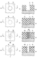
- a PS-b-PMMA film 21 is formed as shown in FIG.
- phase separation occurs in the PS-b-PMMA. Due to this phase separation, as shown in the inset in FIG. 1B, the PS regions DS and the PMMA regions DM are alternately arranged.
- the width of the PS region DS is determined by an integral multiple of the molecular length of PS
- the width of the PMMA region DM is determined by an integral multiple of the molecular length of PMMA
- the PMMA area DM is repeatedly arranged at a predetermined pitch (the width of the PS area DS + the width of the PMMA area DM). Further, since the width of the PS region DS is determined by the number of polymerization of PS molecules and the width of the PMMA region DM is determined by the number of polymerization of PMMA molecules, a desired pattern can be determined by adjusting the number of polymerization. Note that it is preferable to form a guide pattern on the surface of the wafer W in order to arrange the PS region DS and the PMMA region DM of PS-b-PMMA in a predetermined pattern.
- the light source L irradiates ultraviolet light under an inert gas atmosphere such as.
- ultraviolet light will not be specifically limited if it has the wavelength component which belongs to an ultraviolet light area
- an Xe excimer lamp that emits ultraviolet light having a wavelength of 172 nm can be suitably used as the light source L.
- the PS-b-PMMA film 21 When the PS-b-PMMA film 21 is irradiated with ultraviolet light, a cross-linking reaction occurs in PS, so that PS hardly dissolves in an organic solvent, whereas in PMMA, the main chain is cleaved. It is thought that it becomes easy to dissolve in a solvent.
- the irradiation intensity is preferably about 180 mJ or less.
- the PS-b-PMMA film 21 is irradiated with ultraviolet light having a wavelength of 172 nm with a dose amount greater than 180 mJ, when the organic solvent is supplied to the PS-b-PMMA film 21 later, the organic solvent enters the PS region DS.
- the penetration becomes easy, and as a result, the PS region DS swells and the PMMA region DM is hardly removed. Furthermore, when the dose amount of ultraviolet light is larger than 180 mJ, the PMMA region DM may be denatured and solidified, and may be difficult to dissolve in an organic solvent.
- the oxygen concentration in the atmosphere around the wafer W is lowered by the inert gas.
- the oxygen concentration in the inert gas atmosphere is, for example, 400 ppm or less.
- an organic solvent OS is supplied to the PS-b-PMMA film 21.
- the organic solvent OS dissolves the PMMA region DM in the film 21 and the PS region DS remains on the surface of the wafer W.
- the organic solvent OS for example, isopropyl alcohol (IPA) can be preferably used.
- FIG. 2A to 2D are top views, and FIG. 2A to FIG. 2D are II corresponding to FIG. 2A to FIG. 2D. It is sectional drawing along a line.
- a photoresist layer PL is formed on the surface of the wafer W, and a plurality of holes H are formed in the photoresist layer PL as shown in FIGS. 2A and 2A. Two holes H are shown).
- the hole H can be formed by a conventional photolithography technique.
- the inner diameter of the hole H may be about 90 nm, for example.
- toluene is used as a solvent, and PS-b-PMMA is dissolved in this solvent to prepare a coating solution.
- the solid component concentration of PS-b-PMMA in the coating solution may be, for example, 2% by volume.
- a coating liquid is applied onto the photoresist layer PL and the wafer W by, for example, a spin coater to form a PS-b-PMMA film 21.
- the hole H is filled with a film 21 of PS-b-PMMA.
- PS and PMMA are randomly mixed with each other.
- the PS-b-PMMA film 21 is irradiated with ultraviolet light (wavelength 172 nm), for example, for about 10 seconds to about 60 seconds (exposure) using an Xe excimer lamp in an inert gas atmosphere.
- ultraviolet light wavelength 172 nm
- an organic solvent for example, IPA
- IPA is dropped onto the wafer W on which the PS-b-PMMA film 21 is formed, and IPA is deposited on the film 21.
- the IPA is dried by rotating the wafer W. Thereby, as shown in FIGS. 2D and 2D, a hole h defined by the PS region DS is formed.
- the hole h has an inner diameter smaller than the inner diameter (90 nm) of the hole H formed in the photoresist layer PL.
- the inner diameter of the hole h can be adjusted by the mixing ratio of PS and PMMA of PS-b-PMMA, and is about 30 nm in this example.
- a hole having an inner diameter substantially equal to the inner diameter of the hole h is formed in the wafer W.
- a limit dimension for example, about 60 nm
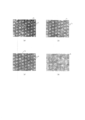
- FIGS. 3A to 3C when the PS-b-PMMA film is exposed to ultraviolet light in an inert gas atmosphere, a hole h is formed by the PS region.
- FIG. 3 (d) when the PS-b-PMMA film is exposed to ultraviolet light in an air atmosphere, the holes are compared with the holes shown in FIGS. 3 (a) to 3 (c). (It should be noted that the magnification of the SEM images in FIG. 3D is larger than the magnification of the SEM images in FIGS. 3A to 3C), and holes are formed. Some parts are not done.
- the PS-b-PMMA film Under an atmosphere containing a high concentration of oxygen (the oxygen concentration in the air is about 20%), the PS-b-PMMA film is excessively oxidized and altered by ultraviolet light, so that the PMMA region is dissolved in IPA. It is thought that it becomes difficult to put out. Further, referring to FIG. 3D, since the surface (the surface of the PS region) is rough, it is considered that the PS region is also excessively oxidized and deteriorated.
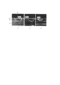
- FIG. 4 is an SEM image showing a cross section of a hole formed according to the above-described method.
- FIG. 4 is a cross-sectional image obtained by cutting the wafer W, the photoresist layer PL, and the PS region along the line II in FIG. 2D and observing with a SEM from a direction perpendicular to the cut surface.
- the PS region in the hole H is removed, and the hole H is visible instead of the hole h.
- FIG. 4A shows a cross-sectional image before development by IPA
- the thickness of the PS region DS on the photoresist layer PL is about 15 nm
- FIG. 4B shows a cross-sectional image after development. Also in FIG. 4B, the thickness of the PS region DS on the photoresist layer PL is about 15 nm. That is, the PS region DS is hardly dissolved in IPA. Considering that the PMMA region is almost completely dissolved by development, the solubility ratio (PMMA solubility / PS solubility) becomes almost infinite.
- FIG. 4 (c) shows the result of developing a PS-b-PMMA film with oxygen plasma using a reactive ion etching (RIE) apparatus.
- RIE reactive ion etching
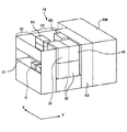
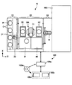
- FIG. 5 is a schematic perspective view showing the pattern forming apparatus 10 according to the present embodiment
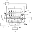
- FIG. 6 is a schematic top view showing the pattern forming apparatus 10. 5 and 6, the pattern forming apparatus 10 includes a cassette station S1, a processing station S2, and an interface station S3.
- a cassette stage 24 and a transfer arm 22 are provided on the cassette stage 24, a plurality (four in the illustrated example) of cassettes C that can accommodate a plurality of (for example, 25) wafers W are placed.
- the direction in which the cassettes C are arranged is referred to as the X direction for the sake of convenience, and the direction orthogonal thereto is referred to as the Y direction. Since the transfer arm 22 transfers the wafer W between the cassette C on the cassette stage 24 and the processing station S2, the transfer arm 22 can move up and down, can move in the X direction, can expand and contract in the Y direction, and can rotate about the vertical axis. It is configured.
- the processing station S2 is coupled to the cassette station S1 on the + Y direction side.
- two coating units 32 are arranged along the Y direction, and above these, the liquid processing unit 31 and the ultraviolet light irradiation unit 40 are arranged in this order in the Y direction (FIG. 5).
- the shelf unit R1 is disposed on the + X direction side with respect to the coating unit 32 and the liquid processing unit 31, and the shelf unit R2 is disposed on the + X direction side with respect to the coating unit 32 and the ultraviolet light irradiation unit 40.
- processing units corresponding to processing performed on the wafer are stacked as will be described later.
- a main transport mechanism MA (FIG. 6) is provided almost at the center of the processing station S 2, and the main transport mechanism MA has an arm 71.
- the arm 71 can move up and down and move in the X and Y directions in order to carry the wafer W in and out of the coating unit 32, the liquid processing unit 31, the ultraviolet light irradiation unit 40, and the processing units of the shelf units R1 and R2. It is possible to rotate around the vertical axis.
- the shelf unit R1 includes a heating unit 61 for heating the wafer W, a cooling unit 62 for cooling the wafer W, a hydrophobizing unit 63 for hydrophobizing the wafer surface, and a wafer W temporarily.
- a pass unit 64 having a stage placed on the substrate and an alignment unit 65 for aligning the wafer W are arranged in the vertical direction.
- a plurality of CHP units 66 for heating and then cooling the wafer W, a pass unit 67 having a stage on which the wafer W is temporarily placed, and the like are arranged in the vertical direction. Note that the types and arrangement of the units in the shelf units R1 and R2 are not limited to those shown in FIG. 7, and may be variously changed.
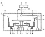
- the liquid processing unit 31 includes a housing 31C, and the spin chuck 2 that rotatably holds the wafer W in the housing 31C and the surface of the wafer W held by the spin chuck 2 are movable.
- the chemical solution supply nozzle 5 for supplying (discharging) the organic solvent to the wafer W and the outer periphery of the wafer W held by the spin chuck 2 are surrounded by the chemical solution supply nozzle 5 and supplied to the surface of the wafer W.
- a cup 6 that receives the organic solvent scattered by the rotation.
- a loading / unloading port (not shown) for the wafer W is provided on one side wall of the housing 31C, and the loading / unloading port can be opened and closed by a shutter (not shown).
- the cup 6 is formed in a cylindrical shape whose bottom surface is closed and whose top surface is open, for example.
- An exhaust port 6 a and a drain port 6 b are provided at the bottom of the cup 6.
- An exhaust pipe 16 connected to an exhaust device (not shown) such as an exhaust pump is connected to the exhaust port 6a.
- a discharge pipe 17 connected to a factory drain is connected to the drain 6b, and the organic solvent recovered by the cup 6 is discharged to the outside of the liquid processing unit 31.
- a servo motor 12 is connected to the spin chuck 2, and the servo motor 12 rotates the spin chuck 2 and the wafer W held by the spin chuck 2 at a predetermined rotation speed.
- three support pins 14 for supporting the wafer W and moving up and down are provided so as to surround the spin chuck 2 (two support pins 14 are shown in FIG. 8).
- the support pin 14 can be moved up and down through a through hole (not shown) formed in the bottom of the cup 6 by a lifting drive mechanism 15 such as a cylinder.
- the support pins 14 can be projected to a position higher than the upper surface of the spin chuck 2 by the lift drive mechanism 15, and the wafer W can be transferred to the spin chuck 2.
- the chemical solution supply nozzle 5 is supported by a rotation / lifting arm 25 that is disposed outside the cup 6 and is connected to a moving mechanism 20 having a horizontal rotation and a lifting function.
- the moving mechanism 20 By the moving mechanism 20, the chemical solution supply nozzle 5 can be moved between an outer position of the cup 6 (position indicated by a dotted line) and a position above the center of the wafer W (position indicated by a solid line).
- the chemical solution supply nozzle 5 is connected to a chemical solution supply source 39 for storing an organic solvent via a chemical solution supply pipe 39C, and can supply the organic solvent supplied from the chemical solution supply source 39 to the wafer W. it can.
- the branch pipe 39B is connected to the chemical liquid supply pipe 39C, and the branch pipe 39B is connected to the additive supply source 39A.
- the additive supply source 39A for example, a hydrophobizing agent (described later) such as a silylating agent is stored, and the hydrophobizing agent is applied to the organic solvent supplied from the chemical solution supply source 39 by switching a valve (not shown). Can be added.
- the chemical solution supply pipe 39C and the branch pipe 39B may be provided with a flow rate regulator for adjusting the flow rates of the organic solvent and the hydrophobizing agent.
- a rinse liquid discharge nozzle 8 for supplying a rinse liquid toward the wafer W held by the spin chuck 2 is provided outside the cup 6.
- the rinse liquid discharge nozzle 8 is provided with a standby portion 8a.
- the rinse liquid discharge nozzle 8 can be moved between the upper center of the wafer W and the standby unit 8a by a moving mechanism and a rotation / lifting arm (not shown) as in the case of the chemical liquid supply nozzle 5.
- the rinsing liquid discharge nozzle 8 is connected to a rinsing liquid supply source (not shown) installed outside the liquid processing unit 31 via a rinsing liquid supply pipe (not shown), thereby rinsing liquid supply source.
- the rinsing liquid supplied from the wafer W can be supplied to the wafer W.
- the coating unit 32 (FIG. 5) has the same configuration as the liquid processing unit 31. However, for example, a solution (coating solution) obtained by dissolving PS-b-PMMA in an organic solvent is stored in the chemical solution supply source 39, and PS-b-PMMA is supplied from the chemical solution supply nozzle 5. A duplicate description of the coating unit 32 is omitted.
- the interface station S3 is coupled to the + Y direction side of the processing station S2, and the exposure apparatus 200 is coupled to the + Y direction side of the interface station S3.
- the exposure apparatus 200 can be used to form the hole H of the photoresist layer PL in the formation of the hole h described with reference to FIG.
- a transport mechanism 76 (FIG. 6) is arranged at the interface station S3.
- the transfer mechanism 76 can move up and down, move in the X direction, and expand and contract in the Y direction to load and unload the wafer W between the pass unit 67 (FIG. 7) of the shelf unit R2 in the processing station S2 and the exposure apparatus 200. It is possible to rotate around the vertical axis.
- the pattern forming apparatus 10 is provided with a control unit 100 for controlling the operation of the entire apparatus.
- the control unit 100 includes a processor formed by a CPU (Central Processing Unit), an MPU (Micro Processing Unit), etc., and a process controller 100a that controls each part or member of the pattern forming apparatus 10, a user interface unit 100b, A storage unit 100c is provided.
- CPU Central Processing Unit
- MPU Micro Processing Unit
- a storage unit 100c is provided.
- the user interface unit 100b includes a keyboard on which a process manager inputs commands to manage the pattern forming apparatus 10, a display for displaying the operation status of the pattern forming apparatus 10, and the like.
- the storage unit 100c stores a recipe in which a control program (software) and processing condition data for realizing various processes executed by the pattern forming apparatus 10 are controlled by the process controller 100a. If necessary, an arbitrary recipe is called from the storage unit 100c according to an instruction from the user interface unit 100b and is executed by the process controller 100a, so that the pattern forming apparatus 10 can perform a desired process under the control of the process controller 100a.
- the function is executed to perform a desired process. That is, for example, the program controls the computer so that the pattern forming apparatus 10 functions as a unit that executes a pattern forming method described later.
- the program (and recipe such as processing condition data) is stored in a computer-readable program recording medium 100d (for example, a hard disk, a compact disk, a magneto-optical disk, a memory card, a flexible disk, etc.). It is installed in the storage unit 100c through an input / output (I / O) device (not shown). Or you may install in the memory
- I / O input / output
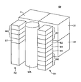
- the ultraviolet light irradiation unit 40 includes a wafer chamber 51 in which the wafer W is accommodated, and a light source chamber 52 that irradiates the wafer W accommodated in the wafer chamber 51 with ultraviolet light. Yes.
- the wafer chamber 51 includes a housing 53, a transmission window 54 that is provided on the ceiling of the housing 53 and can transmit ultraviolet light, and a susceptor 57 on which the wafer W is placed.
- the transmission window 54 is made of, for example, quartz glass.
- the susceptor 57 has a disk shape and has a heater 68 inside.
- the heater 68 is connected to a temperature regulator 69, whereby the temperature of the susceptor 57 is adjusted to a predetermined temperature.
- a plurality of (for example, three) support pins 58 that support the wafer W are provided on the upper surface of the susceptor 57.
- the susceptor 57 has a diameter equal to or slightly larger than that of the wafer W, and is preferably formed of a thermal conductivity having a high thermal conductivity, such as silicon carbide (SiC) or aluminum.
- the plurality of support pins 58 have a function of suppressing excessive heating of the wafer W and promoting cooling of the wafer W after heating. For this reason, it is desirable that the support pins 58 be formed of a material having a high thermal conductivity of, for example, 100 W / (m ⁇ k) or more, for example, silicon carbide (SiC). In order to promote heat conduction from the wafer W to the susceptor 57, the number of support pins 58 is not limited to three, and a larger number of support pins 58 may be provided.
- a cooling water flow channel 55 a is formed inside the base plate 55. Then, cooling water is supplied from the cooling water supply device 70 to the flowing water passage 55a, and the entire base plate 55 is cooled to a predetermined temperature. Moreover, it is preferable that the support
- the wafer chamber 51 is moved up and down through the base plate 55 and the susceptor 57 to support the wafer W from below when the wafer W is loaded and unloaded, and the lift pins 59 are moved up and down.
- a lifting mechanism 60 is provided.
- a wafer W loading / unloading port (not shown) is formed on one side wall of the casing 53, and the wafer W is loaded into the wafer chamber 51 by the arm 71 of the main transfer mechanism MA through the wafer 53. It is carried out from 51.
- a shutter (not shown) is provided at the loading / unloading port, and the loading / unloading port is opened and closed by the shutter. It is preferable that the shutter can close the loading / unloading port in an airtight manner.
- an inert gas introduction port 51A is provided on the side wall of the housing 53, and an inert gas exhaust port 51B is provided on the bottom of the housing 53.
- An inert gas supply source 81 in which an inert gas is stored (filled) is connected to the inert gas introduction port 51A, and the inert gas supply source 81 passes through the inert gas introduction port 51A to the inside of the wafer chamber 51. Active gas is supplied.
- the light source chamber 52 disposed above the wafer chamber 51 includes a light source L that irradiates the wafer W in the wafer chamber 51 with ultraviolet light, and a power source 72 that supplies power to the light source L.
- the light source L is accommodated in the housing 73.
- An irradiation window 74 is provided at the bottom of the housing 73 in order to transmit the ultraviolet light emitted from the light source L to the wafer chamber 51.
- the irradiation window 74 is made of, for example, quartz glass. Ultraviolet light from the light source L is emitted toward the wafer chamber 51 through the irradiation window 74, and ultraviolet light that has passed through the transmission window 54 of the wafer chamber 51 is irradiated onto the wafer W.
- the PS-b-PMMA film formed on the wafer W by the coating unit 32 is heated and exposed as follows. That is, the wafer W on which the PS-b-PMMA film is formed is loaded into the wafer chamber 51 by the arm 71 of the main transfer mechanism MA, received by the lift pins 59, and placed on the support pins 58 on the susceptor 57. After the arm 71 of the main transfer mechanism MA is withdrawn from the wafer chamber 51, the shutter is closed and the inside of the wafer chamber 51 is isolated from the external environment.
- the wafer W supported by the support pins 58 is heated to a predetermined temperature by the heater 68 of the susceptor 57.
- the heat of the wafer W is transmitted to the base plate 55 through the support pins 58 and the susceptor 57, and the wafer W is cooled to, for example, about room temperature (about 23 ° C.). .
- the wafer W After the wafer W reaches about room temperature, power is supplied from the power source 72 to the light source L, and ultraviolet light is emitted from the light source L.
- the ultraviolet light is irradiated on the surface of the wafer W under an inert gas atmosphere through the irradiation window 74 of the light source chamber 52 and the transmission window 54 of the wafer chamber 51. Since the dose required for exposure of the PS-b-PMMA film is determined by “illuminance ⁇ irradiation time”, it is preferable to determine the irradiation time according to the illuminance of the ultraviolet light through, for example, preliminary experiments.
- the wafer W is unloaded from the ultraviolet light irradiation unit 40 by a procedure reverse to that for loading the wafer W. Thereafter, the wafer W is transferred to the liquid processing unit 31 where the PS-b-PMMA film is developed with an organic solvent (eg, IPA). That is, the PMMA region is melted and a pattern constituted by the PS region is obtained.
- the pattern forming apparatus 10 according to the second embodiment the pattern forming method according to the first embodiment can be suitably implemented. That is, the effects and advantages exhibited by the pattern forming method according to the first embodiment are also exhibited by the pattern forming apparatus 10 according to the second embodiment.
- the PS-b-PMMA block copolymer in which phase separation occurs due to heating and the PS region and the PMMA region are regularly arranged.
- This film is exposed to ultraviolet light in an inert gas atmosphere and developed with an organic solvent, whereby a fine pattern of PS regions can be formed.
- the excessive reaction of PMMA and oxygen by ultraviolet light can be suppressed. For this reason, alteration of PMMA can be suppressed, and therefore, a decrease in solubility of PMMA in an organic solvent can be prevented.
- the solubility of PMMA in IPA can be made higher than the solubility of PS, and the solubility ratio can be improved.
- the solubility ratio can be further improved.
- the pattern forming method according to the embodiment of the present invention can also be applied to the formation of line and space patterns.
- the line may fall due to the surface tension of the IPA when the substrate is dried after forming the line composed of the PS region by development with an organic solvent such as IPA.
- a hydrophobizing agent such as a silylating agent
- silylating agents examples include trimethylsilyldimethylamine (TMSDMA), dimethylsilyldimethylamine (DMSDMA), trimethylsilyldiethylamine (TMSDEA), hexamethylzinelazan (HMDS), and trimethylzinelazan (TMDS).
- TMSDMA trimethylsilyldimethylamine
- DMSDMA dimethylsilyldimethylamine
- TMSDEA trimethylsilyldiethylamine
- HMDS hexamethylzinelazan
- TMDS trimethylzinelazan
- the hydrophobizing agent may be added to the organic solvent from the additive supply source 39A of the coating unit 32 in the second embodiment through the branch pipe 39B, or to the chemical solution supply source 39.
- An organic solvent to which a hydrophobizing agent is added may be stored in advance.
- the organic solvent may be rinsed with a liquid having a smaller surface tension.
- a liquid having a smaller surface tension.
- examples of such a liquid include alcohols such as methyl alcohol and ethyl alcohol.
- Such a liquid can be supplied to the wafer W from the rinse liquid discharge nozzle 8 of the liquid processing unit 31 of FIG.
- PS-b-PMMA is exemplified as the block copolymer.
- the present invention is not limited thereto, and examples thereof include polybutadiene-polydimethylsiloxane, polybutadiene-4-vinylpyridine, and polybutadiene-methyl methacrylate.
- the organic solvent for developing the PS-b-PMMA film is not limited to IPA, and for example, methyl alcohol, ethyl alcohol, acetone, xylene, or the like can be used.
- IPA methyl alcohol, ethyl alcohol, acetone, xylene, or the like
- the temperature of the organic solvent may be increased according to the organic solvent used.
- the temperature in the case of IPA, for example, it is preferable to raise the temperature to, for example, 40 ° C. to 60 ° C. By increasing the temperature, the solubility of the PMMA region in the organic solvent can be increased.
- the Xe excimer lamp that emits ultraviolet light having a wavelength of 172 nm is exemplified as the ultraviolet light source L.
- a low-pressure ultraviolet lamp low-pressure mercury lamp
- a KrCl excimer lamp that emits single wavelength light having a wavelength of 222 nm may be used.
- the light source L may be constituted by a lamp having a relatively broad emission spectrum from the far ultraviolet region to the vacuum ultraviolet region and a wavelength cut filter that shields a wavelength longer than, for example, about 230 nm.
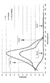
- FIG. 10 is a graph showing the absorption coefficient of PS, PMMA, and PS-b-PMMA with respect to the wavelength of ultraviolet light.
- the PS-b-PMMA as a whole has a high absorption coefficient.
- the absorption coefficient of PMMA itself is extremely low. Therefore, in fact, at 193 nm, the progress of the main chain cleavage reaction in PMMA is slow, and as a result, processing takes time.
- both PS and PMMA show relatively high absorption coefficients, and both the crosslinking reaction in PS and the main chain separation reaction in PMMA proceed relatively quickly. Therefore, the processing time is shortened compared with the case of 193 nm. According to the graph, a relatively high absorption coefficient is obtained for both PS and PMMA even at wavelengths shorter than 172 nm.
- the ultraviolet light irradiation atmosphere requires a lower oxygen concentration. For example, at 160 nm, a substantially vacuum state is required.
- 172 nm ultraviolet light is sufficient even under an inert gas atmosphere such as nitrogen gas as described above.
- the wavelength of the ultraviolet light used in the present invention is most preferably 172 nm.
- the irradiation time of ultraviolet light can be appropriately adjusted according to the block copolymer used, the thickness of the block copolymer, the intensity of the ultraviolet light used, and the like.
- the pattern forming apparatus 10 in which the liquid processing unit 31 and the ultraviolet light irradiation unit 40 are incorporated has been described.
- the liquid processing unit 31 and the ultraviolet light irradiation unit 40 are different from each other in the pattern forming apparatus 10. It may be provided separately from the pattern forming apparatus 10 without being incorporated into the pattern forming apparatus 10.
- the liquid processing unit 31 and the ultraviolet light irradiation unit 40 may be integrally configured.
- the pattern forming apparatus according to another embodiment may be configured by combining the liquid processing unit 31, the coating unit 32, and the ultraviolet light irradiation unit 40.
- the susceptor 57 of the ultraviolet light irradiation unit 40 includes a heater 68, and the block copolymer film is heated in the ultraviolet light irradiation unit 40.
- a heating unit for heating the block copolymer film is provided. You may provide separately from the ultraviolet light irradiation unit 40 instead of in the ultraviolet light irradiation unit 40.
Landscapes
- Engineering & Computer Science (AREA)
- Physics & Mathematics (AREA)
- General Physics & Mathematics (AREA)
- Manufacturing & Machinery (AREA)
- Microelectronics & Electronic Packaging (AREA)
- Condensed Matter Physics & Semiconductors (AREA)
- Computer Hardware Design (AREA)
- Power Engineering (AREA)
- Chemical & Material Sciences (AREA)
- Inorganic Chemistry (AREA)
- Organic Chemistry (AREA)
- Nanotechnology (AREA)
- Analytical Chemistry (AREA)
- Chemical Kinetics & Catalysis (AREA)
- General Chemical & Material Sciences (AREA)
- Photosensitive Polymer And Photoresist Processing (AREA)
- Exposure Of Semiconductors, Excluding Electron Or Ion Beam Exposure (AREA)
- Application Of Or Painting With Fluid Materials (AREA)
- Electrodes Of Semiconductors (AREA)
- Internal Circuitry In Semiconductor Integrated Circuit Devices (AREA)
Priority Applications (2)
| Application Number | Priority Date | Filing Date | Title |
|---|---|---|---|
| US14/389,437 US9618849B2 (en) | 2012-04-06 | 2013-03-28 | Pattern forming method, pattern forming apparatus, and computer readable storage medium |
| KR1020147027564A KR101857323B1 (ko) | 2012-04-06 | 2013-03-28 | 패턴 형성 방법, 패턴 형성 장치 및 컴퓨터 판독 가능 기억 매체 |
Applications Claiming Priority (4)
| Application Number | Priority Date | Filing Date | Title |
|---|---|---|---|
| JP2012087106 | 2012-04-06 | ||
| JP2012-087106 | 2012-04-06 | ||
| JP2012-285132 | 2012-12-27 | ||
| JP2012285132A JP5918122B2 (ja) | 2012-04-06 | 2012-12-27 | パターン形成方法、パターン形成装置、及びコンピュータ可読記憶媒体 |
Publications (1)
| Publication Number | Publication Date |
|---|---|
| WO2013150955A1 true WO2013150955A1 (ja) | 2013-10-10 |
Family
ID=49300445
Family Applications (1)
| Application Number | Title | Priority Date | Filing Date |
|---|---|---|---|
| PCT/JP2013/059264 Ceased WO2013150955A1 (ja) | 2012-04-06 | 2013-03-28 | パターン形成方法、パターン形成装置、及びコンピュータ可読記憶媒体 |
Country Status (5)
| Country | Link |
|---|---|
| US (1) | US9618849B2 (enExample) |
| JP (1) | JP5918122B2 (enExample) |
| KR (1) | KR101857323B1 (enExample) |
| TW (1) | TWI538745B (enExample) |
| WO (1) | WO2013150955A1 (enExample) |
Cited By (3)
| Publication number | Priority date | Publication date | Assignee | Title |
|---|---|---|---|---|
| WO2015075833A1 (ja) * | 2013-11-25 | 2015-05-28 | 東京エレクトロン株式会社 | パターン形成方法及び加熱装置 |
| TWI562239B (en) * | 2013-11-07 | 2016-12-11 | Tokyo Electron Ltd | Pattern forming method and heating device |
| CN109569970A (zh) * | 2018-12-26 | 2019-04-05 | 江苏荣成环保科技股份有限公司 | 一种单面瓦楞机胶桶加热保温装置 |
Families Citing this family (14)
| Publication number | Priority date | Publication date | Assignee | Title |
|---|---|---|---|---|
| US20140273290A1 (en) * | 2013-03-15 | 2014-09-18 | Tokyo Electron Limited | Solvent anneal processing for directed-self assembly applications |
| JP5783472B2 (ja) * | 2013-06-10 | 2015-09-24 | ウシオ電機株式会社 | アッシング装置 |
| JP6235974B2 (ja) | 2014-09-24 | 2017-11-22 | 東京エレクトロン株式会社 | 基板処理方法、プログラム、コンピュータ記憶媒体及び基板処理システム |
| JP6314779B2 (ja) * | 2014-10-01 | 2018-04-25 | 東京エレクトロン株式会社 | 液処理方法、記憶媒体及び液処理装置 |
| JP6495707B2 (ja) | 2015-03-25 | 2019-04-03 | 株式会社Screenホールディングス | 露光装置および基板処理装置 |
| JP6543064B2 (ja) * | 2015-03-25 | 2019-07-10 | 株式会社Screenホールディングス | 露光装置、基板処理装置、基板の露光方法および基板処理方法 |
| TWI723052B (zh) | 2015-10-23 | 2021-04-01 | 日商東京威力科創股份有限公司 | 基板處理方法、程式及電腦記憶媒體 |
| JP6655418B2 (ja) | 2016-02-17 | 2020-02-26 | 株式会社Screenホールディングス | 基板処理装置および基板処理方法 |
| JPWO2017221683A1 (ja) * | 2016-06-24 | 2019-04-04 | 東京エレクトロン株式会社 | 基板処理方法、読み取り可能なコンピュータ記憶媒体及び基板処理システム |
| JP6802667B2 (ja) | 2016-08-18 | 2020-12-16 | 株式会社Screenホールディングス | 熱処理装置、基板処理装置、熱処理方法および基板処理方法 |
| JP6773495B2 (ja) * | 2016-09-15 | 2020-10-21 | 株式会社Screenホールディングス | エッチング装置、基板処理装置、エッチング方法および基板処理方法 |
| JP6683578B2 (ja) | 2016-09-23 | 2020-04-22 | 株式会社Screenホールディングス | 基板処理方法 |
| JP6811638B2 (ja) | 2017-02-14 | 2021-01-13 | 株式会社Screenホールディングス | 基板処理方法及びその装置 |
| EP3528045A1 (en) | 2018-02-16 | 2019-08-21 | IMEC vzw | Method for forming a cross-linked layer |
Citations (4)
| Publication number | Priority date | Publication date | Assignee | Title |
|---|---|---|---|---|
| JP2001151834A (ja) * | 1999-06-07 | 2001-06-05 | Toshiba Corp | パターン形成材料、多孔質構造体の製造方法、パターン形成方法、電気化学セル、中空糸フィルター、多孔質カーボン構造体の製造方法、キャパシタの製造方法、および燃料電池の触媒層の製造方法 |
| WO2011039847A1 (ja) * | 2009-09-29 | 2011-04-07 | 株式会社 東芝 | パターン形成方法 |
| WO2012111694A1 (ja) * | 2011-02-15 | 2012-08-23 | 独立行政法人理化学研究所 | ナノ構造体を表面に備える基板の製造方法 |
| JP2012166302A (ja) * | 2011-02-14 | 2012-09-06 | Tokyo Electron Ltd | パターン形成方法及びパターン形成装置 |
Family Cites Families (7)
| Publication number | Priority date | Publication date | Assignee | Title |
|---|---|---|---|---|
| JP4127682B2 (ja) | 1999-06-07 | 2008-07-30 | 株式会社東芝 | パターン形成方法 |
| JP2001113163A (ja) * | 1999-10-20 | 2001-04-24 | Hoya Schott Kk | 紫外光照射装置及び方法 |
| JP2005142185A (ja) * | 2003-11-04 | 2005-06-02 | Canon Inc | 露光装置及びその環境制御方法 |
| US20060210929A1 (en) * | 2005-03-15 | 2006-09-21 | Canon Kabushiki Kaisha | Photosensitive composition and forming process of structured material using the composition |
| JP4665720B2 (ja) | 2005-11-01 | 2011-04-06 | 株式会社日立製作所 | パターン基板,パターン基板の製造方法、微細金型および磁気記録用パターン媒体 |
| JP4803591B2 (ja) | 2006-06-01 | 2011-10-26 | 東京エレクトロン株式会社 | 溶剤供給方法 |
| JP5300799B2 (ja) * | 2010-07-28 | 2013-09-25 | 株式会社東芝 | パターン形成方法及びポリマーアロイ下地材料 |
-
2012
- 2012-12-27 JP JP2012285132A patent/JP5918122B2/ja active Active
-
2013
- 2013-03-28 KR KR1020147027564A patent/KR101857323B1/ko active Active
- 2013-03-28 WO PCT/JP2013/059264 patent/WO2013150955A1/ja not_active Ceased
- 2013-03-28 US US14/389,437 patent/US9618849B2/en active Active
- 2013-04-01 TW TW102111688A patent/TWI538745B/zh active
Patent Citations (4)
| Publication number | Priority date | Publication date | Assignee | Title |
|---|---|---|---|---|
| JP2001151834A (ja) * | 1999-06-07 | 2001-06-05 | Toshiba Corp | パターン形成材料、多孔質構造体の製造方法、パターン形成方法、電気化学セル、中空糸フィルター、多孔質カーボン構造体の製造方法、キャパシタの製造方法、および燃料電池の触媒層の製造方法 |
| WO2011039847A1 (ja) * | 2009-09-29 | 2011-04-07 | 株式会社 東芝 | パターン形成方法 |
| JP2012166302A (ja) * | 2011-02-14 | 2012-09-06 | Tokyo Electron Ltd | パターン形成方法及びパターン形成装置 |
| WO2012111694A1 (ja) * | 2011-02-15 | 2012-08-23 | 独立行政法人理化学研究所 | ナノ構造体を表面に備える基板の製造方法 |
Cited By (3)
| Publication number | Priority date | Publication date | Assignee | Title |
|---|---|---|---|---|
| TWI562239B (en) * | 2013-11-07 | 2016-12-11 | Tokyo Electron Ltd | Pattern forming method and heating device |
| WO2015075833A1 (ja) * | 2013-11-25 | 2015-05-28 | 東京エレクトロン株式会社 | パターン形成方法及び加熱装置 |
| CN109569970A (zh) * | 2018-12-26 | 2019-04-05 | 江苏荣成环保科技股份有限公司 | 一种单面瓦楞机胶桶加热保温装置 |
Also Published As
| Publication number | Publication date |
|---|---|
| KR20150007279A (ko) | 2015-01-20 |
| US9618849B2 (en) | 2017-04-11 |
| TW201410336A (zh) | 2014-03-16 |
| US20150062545A1 (en) | 2015-03-05 |
| JP5918122B2 (ja) | 2016-05-18 |
| TWI538745B (zh) | 2016-06-21 |
| JP2013232621A (ja) | 2013-11-14 |
| KR101857323B1 (ko) | 2018-05-11 |
Similar Documents
| Publication | Publication Date | Title |
|---|---|---|
| JP5918122B2 (ja) | パターン形成方法、パターン形成装置、及びコンピュータ可読記憶媒体 | |
| US9530645B2 (en) | Pattern forming method, pattern forming apparatus, and non-transitory computer-readable storage medium | |
| JP5484373B2 (ja) | パターン形成方法 | |
| KR101372152B1 (ko) | 패턴 형성 방법 및 중합체 알로이 기재 | |
| JP5827939B2 (ja) | 成膜方法、プログラム、コンピュータ記憶媒体及び成膜装置 | |
| JP5919210B2 (ja) | 基板処理方法、プログラム、コンピュータ記憶媒体及び基板処理システム | |
| TW201445614A (zh) | 用於半導體元件製造上的阻劑硬化及顯影製程 | |
| KR20250138812A (ko) | 마스크 패턴 형성 방법, 기억 매체 및 기판 처리 장치 | |
| JP5758846B2 (ja) | パターン形成方法、パターン形成装置、及びコンピュータ可読記憶媒体 | |
| JP6177958B2 (ja) | パターン形成方法、パターン形成装置、及びコンピュータ可読記憶媒体 | |
| US9748100B2 (en) | Substrate processing method, storage medium and substrate processing system | |
| JP2015179272A (ja) | パターン形成方法、パターン形成装置及びコンピュータ可読記憶媒体 | |
| JP5994736B2 (ja) | 基板処理方法、基板処理装置及び記憶媒体 | |
| TWI813155B (zh) | 基板處理方法以及基板處理裝置 | |
| WO2016047493A1 (ja) | 基板処理方法、コンピュータ記憶媒体及び基板処理システム | |
| WO2020100633A1 (ja) | 基板処理方法及び基板処理装置 | |
| US10586711B2 (en) | Substrate processing method and computer storage medium | |
| JP7603517B2 (ja) | 基板処理方法、および、基板処理装置 | |
| TW201939641A (zh) | 基板處理系統、基板處理裝置及基板處理方法 | |
| JP2013249430A (ja) | パターン形成方法及び加熱装置 | |
| JP2009016653A (ja) | 基板の処理方法及びコンピュータ読み取り可能な記憶媒体 | |
| JPWO2017221683A1 (ja) | 基板処理方法、読み取り可能なコンピュータ記憶媒体及び基板処理システム |
Legal Events
| Date | Code | Title | Description |
|---|---|---|---|
| 121 | Ep: the epo has been informed by wipo that ep was designated in this application |
Ref document number: 13771818 Country of ref document: EP Kind code of ref document: A1 |
|
| ENP | Entry into the national phase |
Ref document number: 20147027564 Country of ref document: KR Kind code of ref document: A |
|
| WWE | Wipo information: entry into national phase |
Ref document number: 14389437 Country of ref document: US |
|
| NENP | Non-entry into the national phase |
Ref country code: DE |
|
| 122 | Ep: pct application non-entry in european phase |
Ref document number: 13771818 Country of ref document: EP Kind code of ref document: A1 |