WO2013141013A1 - 素子収納用パッケージ - Google Patents
素子収納用パッケージ Download PDFInfo
- Publication number
- WO2013141013A1 WO2013141013A1 PCT/JP2013/055955 JP2013055955W WO2013141013A1 WO 2013141013 A1 WO2013141013 A1 WO 2013141013A1 JP 2013055955 W JP2013055955 W JP 2013055955W WO 2013141013 A1 WO2013141013 A1 WO 2013141013A1
- Authority
- WO
- WIPO (PCT)
- Prior art keywords
- terminal
- insulating layer
- terminals
- frame
- storage package
- Prior art date
- Legal status (The legal status is an assumption and is not a legal conclusion. Google has not performed a legal analysis and makes no representation as to the accuracy of the status listed.)
- Ceased
Links
Images





Classifications
-
- H—ELECTRICITY
- H05—ELECTRIC TECHNIQUES NOT OTHERWISE PROVIDED FOR
- H05K—PRINTED CIRCUITS; CASINGS OR CONSTRUCTIONAL DETAILS OF ELECTRIC APPARATUS; MANUFACTURE OF ASSEMBLAGES OF ELECTRICAL COMPONENTS
- H05K1/00—Printed circuits
- H05K1/18—Printed circuits structurally associated with non-printed electric components
- H05K1/181—Printed circuits structurally associated with non-printed electric components associated with surface mounted components
-
- H—ELECTRICITY
- H05—ELECTRIC TECHNIQUES NOT OTHERWISE PROVIDED FOR
- H05K—PRINTED CIRCUITS; CASINGS OR CONSTRUCTIONAL DETAILS OF ELECTRIC APPARATUS; MANUFACTURE OF ASSEMBLAGES OF ELECTRICAL COMPONENTS
- H05K1/00—Printed circuits
- H05K1/16—Printed circuits incorporating printed electric components, e.g. printed resistors, capacitors or inductors
- H05K1/162—Printed circuits incorporating printed electric components, e.g. printed resistors, capacitors or inductors incorporating printed capacitors
-
- H—ELECTRICITY
- H05—ELECTRIC TECHNIQUES NOT OTHERWISE PROVIDED FOR
- H05K—PRINTED CIRCUITS; CASINGS OR CONSTRUCTIONAL DETAILS OF ELECTRIC APPARATUS; MANUFACTURE OF ASSEMBLAGES OF ELECTRICAL COMPONENTS
- H05K1/00—Printed circuits
- H05K1/16—Printed circuits incorporating printed electric components, e.g. printed resistors, capacitors or inductors
- H05K1/167—Printed circuits incorporating printed electric components, e.g. printed resistors, capacitors or inductors incorporating printed resistors
-
- H—ELECTRICITY
- H05—ELECTRIC TECHNIQUES NOT OTHERWISE PROVIDED FOR
- H05K—PRINTED CIRCUITS; CASINGS OR CONSTRUCTIONAL DETAILS OF ELECTRIC APPARATUS; MANUFACTURE OF ASSEMBLAGES OF ELECTRICAL COMPONENTS
- H05K1/00—Printed circuits
- H05K1/18—Printed circuits structurally associated with non-printed electric components
- H05K1/182—Printed circuits structurally associated with non-printed electric components associated with components mounted in printed circuit boards [PCB], e.g. insert-mounted components [IMC]
- H05K1/184—Printed circuits structurally associated with non-printed electric components associated with components mounted in printed circuit boards [PCB], e.g. insert-mounted components [IMC] associated with components inserted in holes through the PCBs and wherein terminals of the components are connected to printed contacts on the walls of the holes or at the edges thereof or protruding over or into the holes
-
- H—ELECTRICITY
- H05—ELECTRIC TECHNIQUES NOT OTHERWISE PROVIDED FOR
- H05K—PRINTED CIRCUITS; CASINGS OR CONSTRUCTIONAL DETAILS OF ELECTRIC APPARATUS; MANUFACTURE OF ASSEMBLAGES OF ELECTRICAL COMPONENTS
- H05K1/00—Printed circuits
- H05K1/18—Printed circuits structurally associated with non-printed electric components
- H05K1/189—Printed circuits structurally associated with non-printed electric components characterised by the use of flexible or folded printed circuits
-
- H—ELECTRICITY
- H10—SEMICONDUCTOR DEVICES; ELECTRIC SOLID-STATE DEVICES NOT OTHERWISE PROVIDED FOR
- H10W—GENERIC PACKAGES, INTERCONNECTIONS, CONNECTORS OR OTHER CONSTRUCTIONAL DETAILS OF DEVICES COVERED BY CLASS H10
- H10W76/00—Containers; Fillings or auxiliary members therefor; Seals
- H10W76/10—Containers or parts thereof
- H10W76/12—Containers or parts thereof characterised by their shape
- H10W76/15—Containers comprising an insulating or insulated base
- H10W76/157—Containers comprising an insulating or insulated base having interconnections parallel to the insulating or insulated base
-
- H—ELECTRICITY
- H05—ELECTRIC TECHNIQUES NOT OTHERWISE PROVIDED FOR
- H05K—PRINTED CIRCUITS; CASINGS OR CONSTRUCTIONAL DETAILS OF ELECTRIC APPARATUS; MANUFACTURE OF ASSEMBLAGES OF ELECTRICAL COMPONENTS
- H05K2201/00—Indexing scheme relating to printed circuits covered by H05K1/00
- H05K2201/03—Conductive materials
- H05K2201/0332—Structure of the conductor
- H05K2201/0335—Layered conductors or foils
- H05K2201/0344—Electroless sublayer, e.g. Ni, Co, Cd or Ag; Transferred electroless sublayer
-
- H—ELECTRICITY
- H05—ELECTRIC TECHNIQUES NOT OTHERWISE PROVIDED FOR
- H05K—PRINTED CIRCUITS; CASINGS OR CONSTRUCTIONAL DETAILS OF ELECTRIC APPARATUS; MANUFACTURE OF ASSEMBLAGES OF ELECTRICAL COMPONENTS
- H05K2201/00—Indexing scheme relating to printed circuits covered by H05K1/00
- H05K2201/10—Details of components or other objects attached to or integrated in a printed circuit board
- H05K2201/10007—Types of components
- H05K2201/10075—Non-printed oscillator
-
- H—ELECTRICITY
- H05—ELECTRIC TECHNIQUES NOT OTHERWISE PROVIDED FOR
- H05K—PRINTED CIRCUITS; CASINGS OR CONSTRUCTIONAL DETAILS OF ELECTRIC APPARATUS; MANUFACTURE OF ASSEMBLAGES OF ELECTRICAL COMPONENTS
- H05K2201/00—Indexing scheme relating to printed circuits covered by H05K1/00
- H05K2201/10—Details of components or other objects attached to or integrated in a printed circuit board
- H05K2201/10007—Types of components
- H05K2201/10083—Electromechanical or electro-acoustic component, e.g. microphone
-
- H—ELECTRICITY
- H05—ELECTRIC TECHNIQUES NOT OTHERWISE PROVIDED FOR
- H05K—PRINTED CIRCUITS; CASINGS OR CONSTRUCTIONAL DETAILS OF ELECTRIC APPARATUS; MANUFACTURE OF ASSEMBLAGES OF ELECTRICAL COMPONENTS
- H05K2201/00—Indexing scheme relating to printed circuits covered by H05K1/00
- H05K2201/10—Details of components or other objects attached to or integrated in a printed circuit board
- H05K2201/10007—Types of components
- H05K2201/10143—Solar cell
-
- H—ELECTRICITY
- H05—ELECTRIC TECHNIQUES NOT OTHERWISE PROVIDED FOR
- H05K—PRINTED CIRCUITS; CASINGS OR CONSTRUCTIONAL DETAILS OF ELECTRIC APPARATUS; MANUFACTURE OF ASSEMBLAGES OF ELECTRICAL COMPONENTS
- H05K2201/00—Indexing scheme relating to printed circuits covered by H05K1/00
- H05K2201/10—Details of components or other objects attached to or integrated in a printed circuit board
- H05K2201/10007—Types of components
- H05K2201/10166—Transistor
-
- H—ELECTRICITY
- H05—ELECTRIC TECHNIQUES NOT OTHERWISE PROVIDED FOR
- H05K—PRINTED CIRCUITS; CASINGS OR CONSTRUCTIONAL DETAILS OF ELECTRIC APPARATUS; MANUFACTURE OF ASSEMBLAGES OF ELECTRICAL COMPONENTS
- H05K2201/00—Indexing scheme relating to printed circuits covered by H05K1/00
- H05K2201/10—Details of components or other objects attached to or integrated in a printed circuit board
- H05K2201/10007—Types of components
- H05K2201/10174—Diode
-
- H—ELECTRICITY
- H05—ELECTRIC TECHNIQUES NOT OTHERWISE PROVIDED FOR
- H05K—PRINTED CIRCUITS; CASINGS OR CONSTRUCTIONAL DETAILS OF ELECTRIC APPARATUS; MANUFACTURE OF ASSEMBLAGES OF ELECTRICAL COMPONENTS
- H05K2201/00—Indexing scheme relating to printed circuits covered by H05K1/00
- H05K2201/10—Details of components or other objects attached to or integrated in a printed circuit board
- H05K2201/10007—Types of components
- H05K2201/10196—Variable component, e.g. variable resistor
Definitions
- the present invention relates to an element storage package that allows an element to be mounted and stored to function as a mounting structure.
- a small device housing package capable of mounting an element such as an IC, a light emitting diode, a piezoelectric element or a crystal resonator has been developed.
- An optical semiconductor package in which an optical semiconductor element such as a laser diode or a photodiode can be mounted has been proposed (for example, Japanese Patent Application Laid-Open No. 2006-66867).
- the electronic component storage package proposed in Japanese Patent Application Laid-Open No. 2006-66867 is provided on each of a metal base, input / output terminals provided on the base, and upper and lower surfaces of the input / output terminals. And a plurality of lead terminals.
- An object of the present invention is to provide an element storage package capable of increasing the number of lead terminals without increasing the size of the package itself.
- An element storage package includes a rectangular substrate having an element mounting region on an upper surface thereof, and a notch formed on a portion of the substrate along the outer periphery of the mounting region. And an input / output terminal provided in the notch and extending from a region surrounded by the frame to a region not surrounded by the frame.
- the input / output terminal includes a first insulating layer, a second insulating layer stacked on the first insulating layer, and a third insulating layer stacked on the second insulating layer.
- the first insulating layer extends outside the frame body more than the second insulating layer and the third insulating layer.
- the second insulating layer extends outside the frame body more than the third insulating layer.
- a plurality of first terminals set to a predetermined potential are provided on the upper surface of the first insulating layer.
- a plurality of second terminals set at a predetermined potential are provided on the lower surface of the first insulating layer.
- a plurality of third terminals through which an AC signal flows is provided on the upper surface of the second insulating layer.
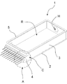
- FIG. 3 is a schematic perspective view of an element storage package according to an embodiment of the present invention, and is an upper perspective view of the front of the input / output terminal as viewed from the rear of the input / output terminal.
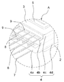
- FIG. 3 is a schematic perspective view of an element storage package according to an embodiment of the present invention, and is an upper perspective view of the rear of the input / output terminal as viewed from the front of the input / output terminal. It is the perspective view of the input / output terminal which expanded the A section of FIG. It is a top view of the element storage package which concerns on one Embodiment of this invention. It is the top view of the input-output terminal which expanded the B section of FIG.
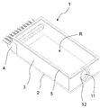
- FIG. 2 is an overview perspective view corresponding to FIG. 1, and is an upper perspective view in which a holding member and a light transmissive member are provided in a through hole.
- FIG. 3 is a schematic perspective view corresponding to FIG. 2, and is an upper perspective view in which a holding member and a light transmissive member are provided in a through hole.
- the element storage package 1 is mounted with, for example, an active element such as a semiconductor element, a transistor, a diode, or a thyristor, or an element composed of a passive element such as a resistor, a capacitor, a solar cell, a piezoelectric element, a crystal oscillator, or a ceramic oscillator. It is used to do.
- the element storage package 1 is suitable for mounting and functioning an element corresponding to high withstand voltage, large current, or high speed and high frequency, and mounts a semiconductor element as an example of the element.
- the element storage package 1 has a rectangular substrate 2 having an element mounting region R on its upper surface, and is formed on the substrate 2 along the outer periphery of the mounting region R, and has a notch C in part.
- a frame 3 and an input / output terminal 4 provided in the notch C and extending from a region surrounded by the frame 3 to a region not surrounded by the frame 3 are provided.
- the substrate 2 is a rectangular metal plate, and is made of, for example, a metal material such as copper, iron, tungsten, molybdenum, nickel, or cobalt, or an alloy containing these metal materials.
- the thermal conductivity of the substrate 2 is set to, for example, 15 W / (m ⁇ K) or more and 450 W / (m ⁇ K) or less.
- the thermal expansion coefficient of the substrate 2 is set to, for example, 3 ⁇ 10 ⁇ 6 / K or more and 28 ⁇ 10 ⁇ 6 / K or less.
- the substrate 2 is manufactured in a predetermined shape by using a conventionally known metal processing method such as rolling or punching for an ingot obtained by casting a molten metal material into a mold and solidifying it.
- a conventionally known metal processing method such as rolling or punching for an ingot obtained by casting a molten metal material into a mold and solidifying it.
- the length of one side of the substrate 2 in a plan view is set to, for example, 5 mm or more and 50 mm or less.
- the thickness in the vertical direction of the substrate 2 is set to, for example, 0.3 mm or more and 5 mm or less.
- a metal layer such as nickel or gold is formed on the surface of the substrate 2 by using an electroplating method or an electroless plating method in order to prevent oxidative corrosion.
- the thickness of the metal layer is set to, for example, 0.5 ⁇ m or more and 9 ⁇ m or less.
- the frame 3 is a member that is connected along the outer periphery of the mounting region R and protects elements mounted on the mounting region R from the outside.
- the frame body 3 has a shape in which a part of a frame shape formed in a quadrangular shape is cut out when viewed in a plan view. Further, the frame body 3 is provided with an input / output terminal 4 in a notch C. Further, the frame 3 may be provided with a through hole H at a location facing the notch C.
- the frame 3 is brazed to the substrate 2 via a brazing material.
- the frame 3 is made of, for example, a metal material such as copper, iron, tungsten, molybdenum, nickel, or cobalt, or an alloy containing these metal materials.
- the frame 3 has a function of efficiently dissipating heat generated from the elements in the frame 3 to the outside of the frame 3.
- the thermal conductivity of the frame 3 is set to, for example, 15 W / (m ⁇ K) or more and 450 W / (m ⁇ K) or less.
- the thermal expansion coefficient of the frame 3 is set to, for example, 3 ⁇ 10 ⁇ 6 / K or more and 28 ⁇ 10 ⁇ 6 / K or less.
- the frame 3 has a size corresponding to the substrate 2 when viewed in plan, and the length of one side is set to, for example, 5 mm or more and 50 mm or less.
- the upper and lower thickness excluding the notch C of the frame 3 is set to, for example, 1 mm or more and 10 mm or less.
- the upper and lower thicknesses including the cutout C of the frame 3 are set to, for example, 5 mm or more and 20 mm or less.
- the thickness of the frame when the frame 3 is viewed in plan is set to, for example, not less than 0.5 mm and not more than 3 mm.
- the input / output terminal 4 is provided in the notch C of the frame 3.
- a light-transmitting member that allows light transmitted from an optical fiber provided outside to pass through the inside of the frame 3 is provided at a position where the through hole H of the frame 3 is formed.
- the through hole H is provided with a holding member 12 into which a light transmissive member 11 such as a lens, plastic, glass, or sapphire substrate can be fitted.
- the holding member 12 may hold the optical fiber close to the end of the optical fiber from the outside of the frame 3 to the vicinity of the light transmissive member 11.
- the frame body 3 has a through hole H formed at a location facing the notch C. Then, as shown in FIG. 8 or FIG. 9, a holding member 12 that holds the light transmissive member 11 in the through hole H is provided.
- the light transmissive member 11 is provided at a height position where light emitted from the optical semiconductor element passes when the optical semiconductor element is mounted in the frame 3. And when an element is an optical semiconductor element, it arrange
- the holding member 12 is made of, for example, a metal such as copper, tungsten, iron, nickel, or cobalt, or an alloy containing a plurality of these metals.
- the light transmissive member 11 is provided on the holding member 12 so as to seal the through hole H.
- the light transmissive member 11 has a function of transmitting light and maintaining airtightness in the frame 3.
- the light transmissive member 11 has a function of converting an optical signal emitted from the optical semiconductor element into condensed light or parallel light. Therefore, the light transmissive member 11 can adjust the optical axis of the optical signal emitted from the optical semiconductor element.
- the input / output terminal 4 may be provided in the notch C facing the light transmissive member 11.
- the length of the element storage package 1 in the direction perpendicular to the optical axis of the through hole H in which the light transmissive member 11 and the optical fiber are held can be suppressed, and the element storage package 1 can be downsized. it can. Therefore, the element storage package 1 can be mounted on the external circuit board with high density.
- the frame 3 and the input / output terminal 4 are provided line-symmetrically in plan view with respect to the optical axis of the through hole H in which the light transmissive member 11 and the optical fiber are held.
- the deformation of the element housing package 1 caused by the difference in thermal expansion coefficient or thermal stress between the substrate 2, the frame body 3, and the input / output terminal 4 becomes line symmetric with respect to the optical axis of the through hole H in plan view. Therefore, the deviation of the optical axis with respect to the optical axis of the through hole H is suppressed. Therefore, the element housing package 1 can smoothly perform optical input / output between the optical semiconductor element housed inside and the optical fiber.
- a seal ring 5 is provided on the frame 3 along the upper surface of the frame 3.
- the seal ring 5 connects the lid when the lid is provided so as to cover the inside of the frame 3.
- the seal ring 5 is made of a metal such as copper, tungsten, iron, nickel, or cobalt having excellent seam weldability with the lid, or an alloy containing a plurality of these metals.
- the input / output terminal 4 is a member provided in the notch C of the frame 3.
- the input / output terminal 4 has a structure in which a plurality of insulating layers are stacked, and is stacked on the first insulating layer 4a, the second insulating layer 4b stacked on the first insulating layer 4a, and the second insulating layer 4b.
- the input / output terminal 4 is provided with a fourth insulating layer 4d on the lower surface of the first insulating layer 4a.
- the first insulating layer 4a extends outside the frame 3 more than the second insulating layer 4b and the third insulating layer 4c, and the second insulating layer 4b extends outside the frame 3 more than the third insulating layer 4c.
- the 4th insulating layer 4d is extended outside the frame 3 rather than the 2nd insulating layer 4b, it is not extended rather than the 1st insulating layer 4a.
- first terminals 6 set at a predetermined potential on the upper surface of the first insulating layer 4a
- second terminals 7 set at a predetermined potential on the lower surface of the first insulating layer 4a
- second insulating layer A plurality of third terminals 8 through which an AC signal flows are provided on the upper surface of 4b.
- the first insulating layer 4a, the second insulating layer 4b, and the third insulating layer 4c are insulating materials, such as an aluminum oxide sintered body, a mullite sintered body, a silicon carbide sintered body, and an aluminum nitride material. It consists of ceramic materials, such as a sintered compact, a silicon nitride sintered body, or glass ceramics.
- the first terminal 6, the second terminal 7, and the third terminal 8 are provided on the upper surface of the first insulating layer 4a, the lower surface of the first insulating layer 4a, and the upper surface of the second insulating layer 4b.
- a metal layer 9 is formed.
- the metal layer 9 is formed in the 1st insulating layer 4a and the 2nd insulating layer 4b corresponding to each terminal.
- a metallized pattern for connecting the frame body 3 via a brazing material is formed on the upper surface of the third insulating layer 4c and the lower surface of the fourth insulating layer 4d.
- the metal layer 9 and the metallized pattern are made of a refractory metal material such as tungsten, molybdenum or manganese.
- the thermal expansion coefficients of the first insulating layer 4a, the second insulating layer 4b, and the third insulating layer 4c made of a ceramic material are set to 3 ⁇ 10 ⁇ 6 / K or more and 8 ⁇ 10 ⁇ 6 / K or less, for example. Has been.
- a method for manufacturing the input / output terminal 4 will be described.
- a thick film forming technique such as a screen printing method or a thin film forming technique such as a vapor deposition method or a sputtering method is used.
- a plurality of metal layers 9 are formed. Further, similarly to the metal layer 9, a metallized pattern is formed on the upper surface of the third insulating layer 4c and the lower surface of the fourth insulating layer 4d.
- the metal layer 9 is provided from one end to the other end of the upper surface of the first insulating layer 4a, provided from one end to the other end of the lower surface of the first insulating layer 4a, and from one end to the other end of the upper surface of the second insulating layer 4b.
- the metallized pattern is formed at a location where it is connected to the frame 3 on the upper surface of the third insulating layer 4c and the lower surface of the fourth insulating layer 4d.
- the first insulating layer 4a, the second insulating layer 4b, the third insulating layer 4c, and the fourth insulating layer 4d are integrated.
- the metal layer 9 is provided so as to extend to the inside and outside surrounded by the frame 3.
- the element in the frame 3 and an external electronic device outside the frame 3 can be electrically connected via the metal layer 9.
- the first terminal 6, the second terminal 7, and the third terminal 8 are members for electrical connection with an external electronic device.
- the first terminal 6, the second terminal 7 and the third terminal 8 are connected to the metal layer 9 via a brazing material.
- Each of the first terminal 6, the second terminal 7, and the third terminal 8 is electrically connected to the metal layer 9.
- the metal layer 9 is provided corresponding to each terminal.
- the metal layer 9 is provided in such a manner that the terminals of the adjacent first terminals 6, the adjacent second terminals 7, and the adjacent third terminals 8 are spaced apart from each other and electrically insulated. Yes.
- the first terminal 6 and the second terminal 7 are set to a predetermined potential that is a fixed value such as a ground or a DC voltage.
- the third terminal 8 is set so that a high-frequency signal as an AC signal flows.
- a part of the first terminal 6 is a ground conductor terminal
- a part of the second terminal 7 is a DC voltage terminal.
- Part of the first terminal 6 is for the ground conductor
- part of the second terminal 7 is for DC voltage
- the third terminal 8 is for AC signal, so that it is particularly between the second terminal 7 below the third terminal 8.
- each of the plurality of third terminals 8 is disposed between the plurality of first terminals 6 in plan view, and the distance between the third terminals 8 and the adjacent first terminals 6 is set. They are arranged to be the same. That is, the third terminal 8 is disposed in the center between the plurality of first terminals 6 in plan view.
- the distance between the first terminal 6 and the third terminal 8 is reduced.
- the electromagnetic field coupling with the third terminal 8 is strengthened, and the mismatch of the impedance of the third terminal 8 is caused by the fluctuation of the capacitance caused by the coupling, and the electromagnetic field coupling between the first terminal 6 and the third terminal 8 is also caused. Resonance is likely to occur. Further, when the size of the first terminal 6 or the third terminal 8 is reduced in order to reduce the capacity component that increases as the distance between the first terminal 6 and the third terminal 8 becomes smaller, Bond strength and bondability at the joint between the first terminal 6 and the third terminal 8 and the input / output terminal 4 and the external circuit board deteriorate.
- the AC signal transmitted through the third terminal 8 is not easily transmitted efficiently. Furthermore, a noise signal is likely to be added to the AC signal transmitted through the third terminal 8. Further, poor bonding is likely to occur between the first terminal 6 or the third terminal 8 and the input / output terminal 4 and the external substrate. As a result, there is a problem that a high-frequency signal composed of an AC signal cannot be input / output normally and accurately between the element stored in the element storage package 1 and the external circuit board connected to the third terminal 8. Likely to happen.
- the third terminal 8 and the first terminal 6 adjacent thereto are arranged.
- the spacing is not the same, and the electromagnetic field distribution between the third terminal 8 and the adjacent first terminal 6 is symmetric with respect to the vertical plane with respect to the second insulating plate 4b along the length direction of the third terminal 8.
- the electromagnetic field distribution between the third terminal 8 and the adjacent first terminal 6 is biased.
- the third terminal 8 is arranged so as not to overlap the first terminal 6, the distance between the third terminal 8 and the first terminal 6 is increased, and the third terminal 8 and the first terminal 6 adjacent thereto are arranged.
- the intervals are the same. This suppresses impedance mismatch at the third terminal 8 caused by electromagnetic coupling between the third terminal 8 and the first terminal 6 and a resonance phenomenon caused by electromagnetic coupling between the first terminal 6 and the third terminal 8.
- the AC signal transmitted from the third terminal 8 can be transmitted efficiently. As a result, it is difficult for a noise signal to be added to the AC signal transmitted through the third terminal 8, and the AC signal is generated between the element stored in the element storage package 1 and the external circuit board connected to the third terminal 8. It is possible to input and output high-frequency signals normally and accurately.
- each of the plurality of third terminals 8 is disposed between the plurality of second terminals 7 in a plan view so that the distance between the third terminal 8 and the first terminal 6 adjacent thereto is the same. Is arranged. That is, the third terminal 8 is disposed in the center between the plurality of first terminals 6 in plan view.
- the third terminal 8 is disposed so as not to overlap the second terminal 7, the distance between the third terminal 8 and the second terminal 7 is increased, and the distance between the third terminal 8 and the second terminal 7 adjacent thereto is increased.
- impedance mismatch at the third terminal 8 caused by electromagnetic coupling between the third terminal 8 and the second terminal 7 and a resonance phenomenon caused by electromagnetic coupling between the second terminal 7 and the third terminal 8 are suppressed. can do.
- the AC signal transmitted at the third terminal 8 is efficiently transmitted and the noise signal is hardly added, and the element housed in the element housing package 1 and the external circuit board connected to the third terminal 8 are A high-frequency signal composed of an AC signal can be input and output normally and accurately.
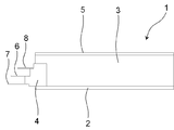
- the first terminal 6, the second terminal 7, and the third terminal 8 extend in the planar direction along the upper surface of the substrate 2, as shown in FIG. Further, the distance between the first terminal 6 and the second terminal 7 in the vertical direction is, for example, not less than 0.3 mm and not more than 3 mm, and is set to be constant. The distance between the first terminal 6 and the second terminal 7 in the vertical direction is constant, and the flexible printed circuit board on which the wiring pattern is formed on the upper and lower surfaces of the outside is connected to the first terminal 6 and the second terminal 7. Can be sandwiched between them. Further, each of the first terminal 6 and the second terminal 7 is electrically connected to a wiring pattern formed on the upper and lower surfaces of the flexible printed board.
- the plurality of second terminals 7 extend outside the frame body 3 from the plurality of first terminals 6 in plan view.
- the second terminal 7 extends beyond the first terminal 6, so that it touches the upper surface of the second terminal 7, and the first terminal 6 extends along the upper surface of the second terminal 7. Since it can be slid so as to be interposed between the second terminals 7, the flexible printed circuit board can be easily installed between the first terminals 6 and the second terminals 7, and the flexible printed circuit board is electrically connected to the input / output terminals 4. The time required to connect to can be reduced. Then, the flexible printed circuit board can be sandwiched between the first terminal 6 and the second terminal 7, and then the first terminal 6 and the second terminal 7 are formed on the upper and lower surfaces of the flexible printed circuit board via solder. It can be electrically connected to the pattern.
- the plurality of first terminals 6 may extend outside the frame body 3 from the plurality of second terminals 7 in plan view. Since the first terminal 6 extends from the second terminal 7, for example, through portions corresponding to the positions of the respective terminals when the input / output terminal 4 is viewed from the side opposite to the through hole H are formed.
- a flexible printed circuit board formed with a wiring pattern electrically connected to the through portion is inserted into each through portion from the opposite direction of the through hole H and electrically connected to each terminal at once.
- the first terminal 6 having a small distance between the second terminal 7 and the third terminal 8 is first inserted into the through portion, so that the second terminal 7 and the third terminal 8 corresponding to the first terminal 6 are inserted. The displacement of the penetrating part can be reduced.
- the first terminal 6 and the second terminal 7 are aligned with each other.
- the positional deviation from the penetrating portion can be further reduced.
- the through holes corresponding to the three terminals 8 are aligned, and the terminals can be electrically connected to the flexible printed circuit board at a time, so that the manufacturing lead time of the mounting structure can be greatly shortened.
- a plurality of types of terminals can be arranged at different height positions with respect to the input / output terminals 4, and the number of lead terminals can be increased without increasing the size of the package itself. Can do. Further, impedance mismatch at the third terminal 8 due to electromagnetic coupling between the third terminal 8 and the first terminal 6 and the second terminal 7 adjacent thereto, and the first terminal 6 and the second terminal 7 and the second terminal 7 A resonance phenomenon caused by electromagnetic coupling with the three terminals 8 is suppressed, an AC signal transmitted through the third terminal 8 is efficiently transmitted and a noise signal is hardly added, and the element housed in the element housing package 1 And a high-frequency signal composed of an alternating current signal can be input / output normally and accurately between the external circuit board connected to the third terminal 8.
- each of the substrate 2, the frame body 3, and the input / output terminal 4 is prepared.
- Each of the substrate 2 and the frame 3 is manufactured in a predetermined shape by using a metal processing method on a solidified ingot obtained by casting a molten metal material into a mold.
- the input / output terminals 4 are prepared with ceramic green sheets corresponding to the respective insulating layers.
- a metal layer 9 made of a metal paste in which an organic solvent containing molybdenum or manganese is applied is formed on the ceramic green sheet using, for example, a screen printing method.
- the input / output terminal 4 is formed by firing the laminated ceramic green sheets. Further, a metallized pattern is formed on the surface of the input / output terminal 4 that becomes a joint surface with the frame 3 using a screen printing method. Further, various terminals are connected to the metal layer 9 of the input / output terminal 4 with a brazing material. In this way, the input / output terminal 4 can be manufactured.
- the prepared frame 3 is connected to the through hole H of the frame 3 by fitting the holding member 12 on which the light transmissive member 11 is mounted via a brazing material.
- each of the prepared substrate 2, frame 3 and input / output terminal 4 is connected via a brazing material.
- the input / output terminals 4 are placed on the substrate 2, and the frame 3 is placed on the substrate 2 so that the input / output terminals 4 are inserted into the notches C. And connect.
- the element storage package 1 can be manufactured.
- an insulating wiring board is provided in the mounting region R of the element housing package 1, the elements are mounted on the wiring board via solder, and the elements, the wiring board, and the input / output terminals 4 are electrically connected via bonding wires.
- the mounting structure can be manufactured by covering the element storage package with a lid.
- FIG. 7 is a side view of the element storage package 1 according to a modification, and corresponds to FIG.
- the second terminal 7 extends from the first terminal 6 toward the outside of the frame 3, but the present invention is not limited thereto.
- the outer end of the frame 3 of the first terminal 6 extends outward from the outer end of the frame 3 of the second terminal 7. Also good.
- the first terminal 6 is provided on the exposed upper surface of the first insulating layer 4a of the input / output terminal 4, and the second terminal 7 is provided on the exposed lower surface of the first insulating layer 4a of the input / output terminal 4.
- One end of the first terminal 6 is provided so as to extend further out of the frame body 3 than one end of the second terminal 7. That is, one end of the first terminal 6 extends toward the outside of the frame body 3 from one end of the second terminal 7.
- the other end of the first terminal 6 is disposed so as to overlap the other end of the second terminal 7 in plan view.
- the difference between one end of the first terminal 6 and one end of the second terminal 7 is set to, for example, 1 mm or more and 5 mm or less.
- one end of the first terminal 6 extends toward the outside of the frame body 3 from one end of the second terminal 7, so that an external member is directed from the upper side of the first terminal 6 toward the first terminal 6. Even if the contact is close and the force is applied in the direction from the first terminal 6 to the second terminal 7, the possibility that the tip of the first terminal 6 contacts the second terminal 7 is reduced.
- one end of the first terminal 6 extends toward the outside of the frame body 3 from one end of the second terminal 7, so that an external member is directed from the upper side of the first terminal 6 toward the first terminal 6. Even if a force acts in the direction from the first terminal 6 to the second terminal 7 due to the close contact, the possibility that the tip of the first terminal 6 contacts the second terminal 7 is suppressed.
- the distal end portion of the first terminal 6 bends or deforms in the direction of the second terminal 7 by the distance between the first terminal 6 and the second terminal 7, the distal end portion of the first terminal 6 remains the second terminal. 7 is difficult to touch.
- the tip of the first terminal 6 is the first terminal 6 and the second terminal 7.
- the tip of the first terminal 6 tends to come into contact with the second terminal 7 when it is bent or deformed in the direction of the second terminal 7 by the distance of. Therefore, when one end of the first terminal 6 extends toward the outside of the frame 3 rather than one end of the second terminal 7, a force acting in the direction from the first terminal 7 to the second terminal 8 is used. It becomes difficult for the first terminal 6 to contact the second terminal 7.
- the probe can be easily applied from above and below so as to sandwich one end of the first terminal 6 therebetween. Therefore, the continuity check of the first terminal 6 can be easily performed. If the second terminal 7 is longer than the first terminal 6, it is difficult to sandwich the first terminal 6 from above and below, and the second terminal 7 and the probe can easily come into contact with each other. Therefore, by making the first terminal 6 longer than the second terminal 7, the continuity check of the first terminal 6 can be facilitated.
- the first terminal 6 since the first terminal 6 is longer than the second terminal 7 and the third terminal 8, the first terminal 6 can be easily connected to the flexible substrate 10 which is easily bent.
- the first terminal 6 In order to connect the flexible substrate 10 and the input / output terminal 4 which are easily bent, the first terminal 6 is inserted into the conduction hole p1, and then the conduction holes p2 and p3 of the flexible substrate 10 which are bent are connected to the second terminal 7 and the third terminal. Align with the terminal 8. Then, each terminal can be connected to the flexible substrate 10 by inserting the second terminal 7 into the conduction hole p2 and further inserting the third terminal 8 into the conduction hole p3.
- the order in which the terminals are inserted into the flexible substrate 10 is the second terminal 7 or the third terminal 8 first. Positioning to insert the terminal into the conductive hole of the flexible substrate 10 that is easily deformed becomes difficult. Therefore, by making the first terminal 6 longer than the second terminal 7 and the third terminal 8, the first terminal 6 is first inserted into the conduction hole p1, and the conduction holes of the second terminal 7 and the third terminal 8 are inserted. Can be easily aligned.
- the vertical distance between the first terminal 6, the second terminal 7, and the third terminal 8 is provided so as to increase as the lengths of the first terminal 6, the second terminal 7, and the third terminal 8 become shorter. May be.
- the flexible substrate 10 positioned between the first terminal 6, the second terminal 7, and the third terminal 8 can be displaced as the distance between the first terminal 6, the second terminal 7, and the third terminal 8 increases. Becomes larger.
- the stress generated in the flexible substrate 10 due to the difference in length between the first terminal 6, the second terminal 7 and the third terminal 8 is the distance between the first terminal 6, the second terminal 7 and the third terminal 8. It is relieved by the displacement of the flexible substrate 10 which becomes larger according to the above. Therefore, the stress is suppressed from concentrating on a part of the flexible substrate 10.
Landscapes
- Engineering & Computer Science (AREA)
- Microelectronics & Electronic Packaging (AREA)
- Piezo-Electric Or Mechanical Vibrators, Or Delay Or Filter Circuits (AREA)
- Semiconductor Lasers (AREA)
- Shielding Devices Or Components To Electric Or Magnetic Fields (AREA)
- Light Receiving Elements (AREA)
Abstract
Description
素子収納用パッケージ1は、例えば、半導体素子、トランジスタ、ダイオードまたはサイリスタ等の能動素子、あるいは抵抗器、コンデンサ、太陽電池、圧電素子、水晶振動子またはセラミック発振子等の受動素子からなる素子を実装するのに用いるものである。素子収納用パッケージ1では、高耐圧化、大電流化または高速・高周波化に対応している素子を実装して機能させるのに適しており、素子の一例として半導体素子を実装するものである。また、素子収納用パッケージ1は、上面に素子の実装領域Rを有する矩形状の基板2と、基板2上であって実装領域Rの外周に沿って形成され、一部に切欠きCを有する枠体3と、切欠きCに設けられ、枠体3で囲まれる領域から枠体3で囲まれない領域にまで延在する入出力端子4と、を備えている。
ここで、図1または図2に示す素子収納用パッケージ1の製造方法を説明する。まず、基板2、枠体3および入出力端子4のそれぞれを準備する。基板2および枠体3のそれぞれは、溶融した金属材料を型枠に鋳込んだ固化させたインゴットに対して、金属加工法を用いることで、所定形状に製作される。
本発明は上述の実施の形態に限定されるものではなく、本発明の要旨を逸脱しない範囲において種々の変更、改良等が可能である。以下、本実施形態の変形例について説明する。なお、本実施形態の変形例に係る素子収納用パッケージおよび実装構造体のうち、本実施形態に係る素子収納用パッケージ1および実装構造体と同様な部分については、同一の符号を付して適宜説明を省略する。図7は、一変形例に係る素子収納用パッケージ1の側面図であって、図6に相当する図面である。
Claims (8)
- 上面に素子の実装領域を有する矩形状の基板と、
前記基板上に前記実装領域の外周に沿って設けられた、一部に切欠きを有する枠体と、
前記切欠きに設けられた、前記枠体で囲まれる領域から前記枠体で囲まれない領域にまで延在する入出力端子とを備え、
前記入出力端子は、第1絶縁層と、前記第1絶縁層上に積層された第2絶縁層と、前記第2絶縁層上に積層された第3絶縁層とを含んでおり、
前記第1絶縁層は前記第2絶縁層および前記第3絶縁層よりも前記枠体外に延在して、前記第2絶縁層は前記第3絶縁層よりも前記枠体外に延在しているとともに、前記第1絶縁層の上面に所定電位に設定される複数の第1端子が、前記第1絶縁層の下面に所定電位に設定される複数の第2端子が、前記第2絶縁層の上面に交流信号が流れる複数の第3端子がそれぞれ設けられていることを特徴とする素子収納用パッケージ。 - 請求項1に記載の素子収納用パッケージであって、
前記複数の第3端子のそれぞれは、前記複数の第1端子同士の間に配置されていることを特徴とする素子収納用パッケージ。 - 請求項2に記載の素子収納用パッケージであって、
前記複数の第1端子と前記複数の第2端子とは、上下に重なっていることを特徴とする素子収納用パッケージ。 - 請求項3に記載の素子収納用パッケージであって、
前記複数の第1端子の一端は、前記複数の第2端子の一端よりも前記枠体外に向かって延在していることを特徴とする素子収納用パッケージ。 - 請求項1に記載の素子収納用パッケージであって、
前記第1端子は、接地導体用端子であって、前記第2端子は直流電圧用端子であることを特徴とする素子収納用パッケージ。 - 請求項1に記載の素子収納用パッケージであって、
前記枠体は、前記切欠きと対向する箇所に貫通孔が形成されており、
前記貫通孔に光透過性部材を保持した保持部材が設けられていることを特徴とする素子収納用パッケージ。 - 請求項6に記載の素子収納用パッケージであって、
前記素子は光半導体素子であって、前記光透過性部材の光軸と一致する前記実装領域に配置されることを特徴とする素子収納用パッケージ。 - 請求項1ないし請求項7のいずれかに記載の素子収納用パッケージであって、
前記入出力端子は、フレキシブル基板と電気的に接続されることを特徴とする素子収納用パッケージ。
Priority Applications (3)
| Application Number | Priority Date | Filing Date | Title |
|---|---|---|---|
| US14/382,801 US9408307B2 (en) | 2012-03-22 | 2013-03-05 | Device housing package |
| JP2014506121A JP5823023B2 (ja) | 2012-03-22 | 2013-03-05 | 素子収納用パッケージ |
| CN201380010881.9A CN104126224B (zh) | 2012-03-22 | 2013-03-05 | 元件收纳用封装件 |
Applications Claiming Priority (4)
| Application Number | Priority Date | Filing Date | Title |
|---|---|---|---|
| JP2012-065758 | 2012-03-22 | ||
| JP2012065758 | 2012-03-22 | ||
| JP2012-255862 | 2012-11-22 | ||
| JP2012255862 | 2012-11-22 |
Publications (1)
| Publication Number | Publication Date |
|---|---|
| WO2013141013A1 true WO2013141013A1 (ja) | 2013-09-26 |
Family
ID=49222475
Family Applications (1)
| Application Number | Title | Priority Date | Filing Date |
|---|---|---|---|
| PCT/JP2013/055955 Ceased WO2013141013A1 (ja) | 2012-03-22 | 2013-03-05 | 素子収納用パッケージ |
Country Status (4)
| Country | Link |
|---|---|
| US (1) | US9408307B2 (ja) |
| JP (1) | JP5823023B2 (ja) |
| CN (1) | CN104126224B (ja) |
| WO (1) | WO2013141013A1 (ja) |
Cited By (3)
| Publication number | Priority date | Publication date | Assignee | Title |
|---|---|---|---|---|
| US20170069556A1 (en) * | 2014-03-13 | 2017-03-09 | Kyocera Corporation | Electronic component housing package and electronic device |
| JP2019169607A (ja) * | 2018-03-23 | 2019-10-03 | 京セラ株式会社 | 半導体素子用パッケージおよび半導体装置 |
| JPWO2021166498A1 (ja) * | 2020-02-18 | 2021-08-26 |
Families Citing this family (5)
| Publication number | Priority date | Publication date | Assignee | Title |
|---|---|---|---|---|
| JP3232797B2 (ja) | 1993-08-16 | 2001-11-26 | 富士電機株式会社 | キャリアセンス付き受信回路 |
| JP6151654B2 (ja) * | 2014-02-25 | 2017-06-21 | 日東電工株式会社 | 配線回路基板およびその製造方法 |
| KR102356636B1 (ko) * | 2015-06-26 | 2022-01-28 | 삼성전자주식회사 | 입력 장치, 그 입력 장치로부터 신호를 입력받는 전자기기 및 그 제어방법 |
| EP3876272A4 (en) * | 2018-10-30 | 2022-08-17 | Kyocera Corporation | HOUSING FOR HOUSING AN ELECTRONIC COMPONENT AND ELECTRONIC DEVICE |
| GB2600918B (en) * | 2020-10-30 | 2022-11-23 | Npl Management Ltd | Ion microtrap assembly and method of making of making such an assembly |
Citations (3)
| Publication number | Priority date | Publication date | Assignee | Title |
|---|---|---|---|---|
| JP2004356391A (ja) * | 2003-05-29 | 2004-12-16 | Kyocera Corp | 半導体素子収納用パッケージおよび半導体装置 |
| JP2006210672A (ja) * | 2005-01-28 | 2006-08-10 | Kyocera Corp | 接続端子ならびにこれを用いた電子部品収納用パッケージおよび電子装置 |
| WO2009057691A1 (ja) * | 2007-10-30 | 2009-05-07 | Kyocera Corporation | 接続端子及びこれを用いたパッケージ並びに電子装置 |
Family Cites Families (7)
| Publication number | Priority date | Publication date | Assignee | Title |
|---|---|---|---|---|
| WO2001053194A1 (fr) * | 2000-01-19 | 2001-07-26 | Mitsubishi Denki Kabushiki Kaisha | Microdispositif et son procede de production |
| JP2004003886A (ja) * | 2002-05-31 | 2004-01-08 | Matsushita Electric Works Ltd | センサパッケージ |
| US6992250B2 (en) | 2004-02-26 | 2006-01-31 | Kyocera Corporation | Electronic component housing package and electronic apparatus |
| JP4480598B2 (ja) | 2004-02-26 | 2010-06-16 | 京セラ株式会社 | 電子部品収納用パッケージおよび電子装置 |
| WO2006001389A1 (ja) * | 2004-06-28 | 2006-01-05 | Mitsubishi Denki Kabushiki Kaisha | 多層誘電体基板および半導体パッケージ |
| JP4947967B2 (ja) * | 2005-12-12 | 2012-06-06 | 富士通株式会社 | 回路モジュール |
| US7947908B2 (en) * | 2007-10-19 | 2011-05-24 | Advantest Corporation | Electronic device |
-
2013
- 2013-03-05 JP JP2014506121A patent/JP5823023B2/ja active Active
- 2013-03-05 WO PCT/JP2013/055955 patent/WO2013141013A1/ja not_active Ceased
- 2013-03-05 CN CN201380010881.9A patent/CN104126224B/zh not_active Expired - Fee Related
- 2013-03-05 US US14/382,801 patent/US9408307B2/en active Active
Patent Citations (3)
| Publication number | Priority date | Publication date | Assignee | Title |
|---|---|---|---|---|
| JP2004356391A (ja) * | 2003-05-29 | 2004-12-16 | Kyocera Corp | 半導体素子収納用パッケージおよび半導体装置 |
| JP2006210672A (ja) * | 2005-01-28 | 2006-08-10 | Kyocera Corp | 接続端子ならびにこれを用いた電子部品収納用パッケージおよび電子装置 |
| WO2009057691A1 (ja) * | 2007-10-30 | 2009-05-07 | Kyocera Corporation | 接続端子及びこれを用いたパッケージ並びに電子装置 |
Cited By (9)
| Publication number | Priority date | Publication date | Assignee | Title |
|---|---|---|---|---|
| US20170069556A1 (en) * | 2014-03-13 | 2017-03-09 | Kyocera Corporation | Electronic component housing package and electronic device |
| EP3118895A4 (en) * | 2014-03-13 | 2017-11-15 | Kyocera Corporation | Package for storing electronic component, and electronic device |
| US9935025B2 (en) * | 2014-03-13 | 2018-04-03 | Kyocera Corporation | Electronic component housing package and electronic device |
| JP2019169607A (ja) * | 2018-03-23 | 2019-10-03 | 京セラ株式会社 | 半導体素子用パッケージおよび半導体装置 |
| JP2021170675A (ja) * | 2018-03-23 | 2021-10-28 | 京セラ株式会社 | 半導体素子用パッケージおよび半導体装置 |
| JP7196249B2 (ja) | 2018-03-23 | 2022-12-26 | 京セラ株式会社 | 半導体素子用パッケージおよび半導体装置 |
| JPWO2021166498A1 (ja) * | 2020-02-18 | 2021-08-26 | ||
| WO2021166498A1 (ja) * | 2020-02-18 | 2021-08-26 | 京セラ株式会社 | 配線基体および電子装置 |
| JP7432703B2 (ja) | 2020-02-18 | 2024-02-16 | 京セラ株式会社 | 配線基体および電子装置 |
Also Published As
| Publication number | Publication date |
|---|---|
| JPWO2013141013A1 (ja) | 2015-08-03 |
| US9408307B2 (en) | 2016-08-02 |
| CN104126224A (zh) | 2014-10-29 |
| CN104126224B (zh) | 2017-02-22 |
| JP5823023B2 (ja) | 2015-11-25 |
| US20150016074A1 (en) | 2015-01-15 |
Similar Documents
| Publication | Publication Date | Title |
|---|---|---|
| JP5823023B2 (ja) | 素子収納用パッケージ | |
| CN106062946B (zh) | 电子部件收纳用封装件以及电子装置 | |
| JP6243510B2 (ja) | 電子部品収納用パッケージおよび電子装置 | |
| CN107534021B (zh) | 电子部件搭载用封装体以及使用其的电子装置 | |
| JPWO2018151176A1 (ja) | 熱電素子内蔵パッケージ | |
| US20240321692A1 (en) | Power module | |
| WO2015088028A1 (ja) | 素子収納用パッケージおよび実装構造体 | |
| JP6082114B2 (ja) | 素子収納用パッケージおよび実装構造体 | |
| JP2009283898A (ja) | 電子部品容器体およびそれを用いた電子部品収納用パッケージならびに電子装置 | |
| JP2017120869A (ja) | セラミックパッケージ | |
| US12387990B2 (en) | Electronic component accommodation package and electronic device | |
| JP6030371B2 (ja) | 素子収納用パッケージおよび実装構造体 | |
| JP5969317B2 (ja) | 光半導体素子収納用パッケージおよび実装構造体 | |
| JP2014011271A (ja) | 素子収納用パッケージおよび実装構造体 | |
| JP2019009376A (ja) | 光半導体素子収納用パッケージおよび光半導体装置 | |
| JP5905728B2 (ja) | 素子収納用パッケージ、および実装構造体 | |
| JP6622583B2 (ja) | 配線基板および電子装置 | |
| JP5791258B2 (ja) | 電子部品収納用パッケージおよび実装構造体 | |
| US10388628B2 (en) | Electronic component package | |
| WO2010150729A1 (ja) | 素子収納用パッケージ、及び実装構造体 | |
| JP5791263B2 (ja) | 電子部品収納用パッケージおよび実装構造体 | |
| JP2014049563A (ja) | 電子部品収納用パッケージおよび実装構造体 | |
| JP2013046041A (ja) | 信号伝送路 | |
| JP4214035B2 (ja) | 配線基板および電子装置 | |
| JP4535894B2 (ja) | 配線基板 |
Legal Events
| Date | Code | Title | Description |
|---|---|---|---|
| 121 | Ep: the epo has been informed by wipo that ep was designated in this application |
Ref document number: 13764628 Country of ref document: EP Kind code of ref document: A1 |
|
| ENP | Entry into the national phase |
Ref document number: 2014506121 Country of ref document: JP Kind code of ref document: A |
|
| WWE | Wipo information: entry into national phase |
Ref document number: 14382801 Country of ref document: US |
|
| NENP | Non-entry into the national phase |
Ref country code: DE |
|
| 122 | Ep: pct application non-entry in european phase |
Ref document number: 13764628 Country of ref document: EP Kind code of ref document: A1 |