WO2013065475A1 - 電子顕微法の観察標体、電子顕微法、電子顕微鏡および観察標体作製装置 - Google Patents
電子顕微法の観察標体、電子顕微法、電子顕微鏡および観察標体作製装置 Download PDFInfo
- Publication number
- WO2013065475A1 WO2013065475A1 PCT/JP2012/076704 JP2012076704W WO2013065475A1 WO 2013065475 A1 WO2013065475 A1 WO 2013065475A1 JP 2012076704 W JP2012076704 W JP 2012076704W WO 2013065475 A1 WO2013065475 A1 WO 2013065475A1
- Authority
- WO
- WIPO (PCT)
- Prior art keywords
- sample
- ionic liquid
- electron
- medium containing
- liquid medium
- Prior art date
- Legal status (The legal status is an assumption and is not a legal conclusion. Google has not performed a legal analysis and makes no representation as to the accuracy of the status listed.)
- Ceased
Links
Images


Classifications
-
- H—ELECTRICITY
- H01—ELECTRIC ELEMENTS
- H01J—ELECTRIC DISCHARGE TUBES OR DISCHARGE LAMPS
- H01J37/00—Discharge tubes with provision for introducing objects or material to be exposed to the discharge, e.g. for the purpose of examination or processing thereof
- H01J37/26—Electron or ion microscopes; Electron or ion diffraction tubes
- H01J37/261—Details
-
- G—PHYSICS
- G01—MEASURING; TESTING
- G01B—MEASURING LENGTH, THICKNESS OR SIMILAR LINEAR DIMENSIONS; MEASURING ANGLES; MEASURING AREAS; MEASURING IRREGULARITIES OF SURFACES OR CONTOURS
- G01B15/00—Measuring arrangements characterised by the use of electromagnetic waves or particle radiation, e.g. by the use of microwaves, X-rays, gamma rays or electrons
- G01B15/02—Measuring arrangements characterised by the use of electromagnetic waves or particle radiation, e.g. by the use of microwaves, X-rays, gamma rays or electrons for measuring thickness
-
- G—PHYSICS
- G01—MEASURING; TESTING
- G01N—INVESTIGATING OR ANALYSING MATERIALS BY DETERMINING THEIR CHEMICAL OR PHYSICAL PROPERTIES
- G01N23/00—Investigating or analysing materials by the use of wave or particle radiation, e.g. X-rays or neutrons, not covered by groups G01N3/00 – G01N17/00, G01N21/00 or G01N22/00
-
- H—ELECTRICITY
- H01—ELECTRIC ELEMENTS
- H01J—ELECTRIC DISCHARGE TUBES OR DISCHARGE LAMPS
- H01J37/00—Discharge tubes with provision for introducing objects or material to be exposed to the discharge, e.g. for the purpose of examination or processing thereof
- H01J37/02—Details
- H01J37/026—Means for avoiding or neutralising unwanted electrical charges on tube components
-
- H—ELECTRICITY
- H01—ELECTRIC ELEMENTS
- H01J—ELECTRIC DISCHARGE TUBES OR DISCHARGE LAMPS
- H01J37/00—Discharge tubes with provision for introducing objects or material to be exposed to the discharge, e.g. for the purpose of examination or processing thereof
- H01J37/26—Electron or ion microscopes; Electron or ion diffraction tubes
- H01J37/28—Electron or ion microscopes; Electron or ion diffraction tubes with scanning beams
-
- H—ELECTRICITY
- H01—ELECTRIC ELEMENTS
- H01J—ELECTRIC DISCHARGE TUBES OR DISCHARGE LAMPS
- H01J2237/00—Discharge tubes exposing object to beam, e.g. for analysis treatment, etching, imaging
- H01J2237/004—Charge control of objects or beams
- H01J2237/0041—Neutralising arrangements
- H01J2237/0044—Neutralising arrangements of objects being observed or treated
-
- Y—GENERAL TAGGING OF NEW TECHNOLOGICAL DEVELOPMENTS; GENERAL TAGGING OF CROSS-SECTIONAL TECHNOLOGIES SPANNING OVER SEVERAL SECTIONS OF THE IPC; TECHNICAL SUBJECTS COVERED BY FORMER USPC CROSS-REFERENCE ART COLLECTIONS [XRACs] AND DIGESTS
- Y10—TECHNICAL SUBJECTS COVERED BY FORMER USPC
- Y10T—TECHNICAL SUBJECTS COVERED BY FORMER US CLASSIFICATION
- Y10T428/00—Stock material or miscellaneous articles
- Y10T428/24—Structurally defined web or sheet [e.g., overall dimension, etc.]
- Y10T428/24273—Structurally defined web or sheet [e.g., overall dimension, etc.] including aperture
- Y10T428/24322—Composite web or sheet
- Y10T428/24331—Composite web or sheet including nonapertured component
-
- Y—GENERAL TAGGING OF NEW TECHNOLOGICAL DEVELOPMENTS; GENERAL TAGGING OF CROSS-SECTIONAL TECHNOLOGIES SPANNING OVER SEVERAL SECTIONS OF THE IPC; TECHNICAL SUBJECTS COVERED BY FORMER USPC CROSS-REFERENCE ART COLLECTIONS [XRACs] AND DIGESTS
- Y10—TECHNICAL SUBJECTS COVERED BY FORMER USPC
- Y10T—TECHNICAL SUBJECTS COVERED BY FORMER US CLASSIFICATION
- Y10T428/00—Stock material or miscellaneous articles
- Y10T428/26—Web or sheet containing structurally defined element or component, the element or component having a specified physical dimension
- Y10T428/261—In terms of molecular thickness or light wave length
Definitions
- the present invention relates to a microscope technique for observing the surface shape of a sample using electrons.
- SEM scanning electron microscope
- the primary electrons accelerated by the voltage applied to the electron source are focused by an electron lens, and the focused primary electrons are scanned on the sample by a deflector.
- Secondary electrons emitted from the sample by irradiating the primary electrons are detected by a detector.
- the secondary electron signal is detected in synchronization with the scanning signal and constitutes an image.
- the amount of secondary electrons emitted from the sample varies depending on the surface shape of the sample.
- Patent Document 1 discloses a method of applying conductivity to an electron irradiation surface by applying an ionic liquid that hardly volatilizes in a vacuum to a sample.
- Patent Document 2 discloses a low-acceleration SEM that uses a low-acceleration electron and can perform stable observation even when charged.
- An object of the present invention is to provide an electron microscope observation specimen, an electron microscope technique, an electron microscope, and an observation specimen preparation apparatus that solve the above-described problems and suppress image disturbance due to charging.
- an observation specimen for an electron microscopic method is characterized in that the liquid medium containing the ionic liquid on the sample is in the form of a thin film or a retina.
- the thin film or retina of the liquid medium containing the ionic liquid in the observation target is along the surface shape of the sample, is a film thickness that allows transmission of low-acceleration primary electrons, or is coated according to the sample shape. Therefore, a clear edge contrast can be obtained.
- the thickness of the portion where the liquid medium containing the ionic liquid is applied is 1 monolayer or more and 100 monolayer or less.
- One monolayer refers to the thickness of one molecular layer of an ionic liquid.
- the electron microscopic method includes a step of measuring a film thickness of a liquid medium containing an ionic liquid on a sample, and a step of controlling irradiation conditions of primary electrons based on the film thickness of the liquid medium containing the ionic liquid. Is included. According to this method, since the irradiation conditions of the primary electrons can be controlled according to the film thickness of the liquid medium containing the ionic liquid, the edge contrast is improved.
- the electron microscopic method according to the present invention further includes a step of applying a liquid medium containing an ionic liquid to a sample and a step of thinning the liquid medium containing the ionic liquid.
- the state of the film of the liquid medium containing the applied ionic liquid depends on the type of the ionic liquid and the material or shape of the sample. According to this method, the film thickness of the liquid medium containing the ionic liquid can be controlled according to the type and sample of the ionic liquid.
- an observation specimen in which the liquid medium containing the ionic liquid on the sample is in the form of a thin film or a retina is used.
- the step of measuring may be performed a plurality of times. According to this method, since the liquid medium containing the ionic liquid can be processed step by step until the predetermined film thickness is reached, the film thickness controllability of the liquid medium containing the ionic liquid is improved.
- the step of measuring the film thickness of the liquid medium containing the ionic liquid is based on the primary electron acceleration voltage dependence of the secondary electron emission rate that can be analyzed by the pulsed primary electrons, and the ionic liquid May be used to measure the film thickness of the liquid medium containing the.
- the change in the secondary electron emission rate with respect to the acceleration voltage can analyze the acceleration voltage at which the primary electrons pass through the film of the liquid medium containing the ionic liquid, and the ionic liquid can be calculated from the range of the primary electrons at the acceleration voltage.
- the film thickness of the liquid medium containing can be analyzed.
- the step of measuring the film thickness of the liquid medium containing the ionic liquid is based on the dependence of the substrate current on the primary electron acceleration voltage under irradiation of the primary electrons, from the liquid electron medium containing the ionic liquid. What measures a film thickness may be sufficient.
- the displacement current generated by the charge accumulated when the primary electrons are transmitted to the sample is measured as the substrate current.
- the acceleration voltage at which primary electrons pass through the film of the liquid medium containing the ionic liquid can be analyzed by the change of the substrate current with respect to the acceleration voltage, and the liquid containing the ionic liquid can be analyzed from the range of the primary electrons at the acceleration voltage.
- the film thickness of the medium can be analyzed.
- the electron microscope according to the present invention includes an electron source that emits primary electrons, a sample holder that holds a sample, an exhaust chamber that is evacuated by installing the sample holder, and a lens that focuses the primary electrons on the sample.
- a system a deflector that scans the primary electrons, a detector that detects secondary electrons emitted from the sample by the primary electrons, an image generation unit that forms an image by the secondary electrons, and the sample holder
- the measurement mechanism for measuring the film thickness of the liquid medium containing the ionic liquid includes a pulse forming unit that forms pulse electrons obtained by pulsing the primary electrons, and the sample by the pulse electrons.
- a secondary electron signal analyzing unit for analyzing a secondary electron emission rate from a secondary electric signal detected by the detector, and a primary electron from the acceleration voltage dependency of the secondary electron emission rate. May have a secondary electron emission rate analysis unit that analyzes the acceleration voltage that passes through the film of the liquid medium containing the ionic liquid and analyzes the film thickness from the range of primary electrons at the acceleration voltage.
- the measuring mechanism for measuring the film thickness of the liquid medium containing the ionic liquid includes a substrate current measuring unit that measures a substrate current induced when the primary electrons are transmitted to the sample, Analyzing the acceleration voltage at which the primary electrons pass through the film of the liquid medium containing the ionic liquid from the dependence of the substrate current on the acceleration voltage, and measuring the film thickness from the range of the primary electrons at that time You may have.
- the sample holder or the sample chamber for holding the sample may have a coating portion for applying the liquid medium containing the ionic liquid to the observation surface of the sample.
- the sample holder or sample chamber for holding the sample may have a mechanism for thinning the liquid medium containing the ionic liquid on the sample.
- the observation specimen preparation device for producing the observation specimen of the present invention includes an exhaust chamber, an exhaust mechanism, an application unit for applying a liquid medium containing the ionic liquid to the observation surface of the sample, A mechanism for thinning the liquid medium containing the ionic liquid, and a film thickness measuring mechanism for the liquid medium containing the ionic liquid.
- the measurement mechanism that measures the film thickness of the liquid medium containing the ionic liquid includes an electron source that emits primary electrons, and a substrate current measurement unit that measures a substrate current induced when the sample is irradiated with the primary electrons. And a substrate current analysis unit that analyzes the dependency of the substrate current on the primary electron acceleration voltage.
- the observation specimen, electron microscopic method, electron microscope, and observation specimen preparation apparatus of the present invention can suppress charging by primary electrons, obtain a clear edge contrast from the observation specimen, and provide a highly accurate surface shape of the sample. Can be measured.
- FIG. 3 is a top view showing an example of an observation specimen according to the first embodiment of the present invention.
- FIG. 3 is a cross-sectional view showing an example of an observation specimen of Example 1 of the present invention.
- the top view which shows an example of the observation specimen of Example 5 of this invention.
- Sectional drawing which shows an example of the observation specimen of Example 5 of this invention.
- Explanatory drawing which shows the presence or absence of the liquid medium containing the ionic liquid on a sample.
- the figure which shows the time change of the secondary electron signal corresponding to the presence or absence of the liquid medium containing the ionic liquid on a sample.
- the block diagram which shows an example of the electron microscope of Example 1 of this invention.
- Explanatory drawing which shows the cross-section of an observation specimen.
- FIG. 6 is an explanatory diagram showing a relationship between an acceleration voltage of primary electrons and a substrate current in Example 2.
- FIG. 6 shows an SEM image obtained by the electron microscopic method of Example 2.
- FIG. 6 is an explanatory diagram showing a profile of image brightness obtained by the electron microscopic method of Example 2.
- FIG. 6 is an explanatory diagram showing the structure of an observation specimen used in Example 5.
- FIG. 10 is a diagram showing a profile of image brightness of an observation specimen used in Example 5.
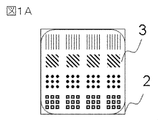
- FIG. 1A shows a top view of an observation specimen in which the liquid medium containing the ionic liquid on the sample is in a thin film form
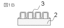
- FIG. 1B shows a cross-sectional view of the observation specimen in which the liquid medium containing the ionic liquid is in a thin film form
- the sample 2 is a sample having a grooved pattern
- the liquid medium 3 containing an ionic liquid is an ionic liquid that is formed into a thin film on the grooved pattern.
- the ionic liquid used in the present invention is, for example, 1-Butyl-3-methylimidazoliumimidazolTetrafluoroborate (1-butyl-3-methylimidazolium tetrafluoroborate), 1-Ethyl-3-methylimidazolium bis (trifluoromethylsulfonyl) imide (1- Butyl-3-methylimidazolium bis (trifluoromethanesulfonyl) imide) and 1-Butyl-3-methylimidazolium bis (trifluoromethylsulfonyl) imide (1-ethyl-3-methylimidazolium bis (trifluoromethanesulfonyl) imide).
- a liquid medium containing an ionic liquid obtained by diluting the ionic liquid with pure water to 10% by weight was used.
- pure water is mixed with the ionic liquid, but ethanol, methanol, acetone, hexane, or the like may be mixed.
- fine particles having different secondary electron emission rates from the ionic liquid may be mixed in the ionic liquid so that the contrast of the image can be clearly obtained.
- the secondary electron emission rate is obtained by dividing the number of emitted secondary electrons by the number of irradiated primary electrons.
- the liquid medium containing an ionic liquid is a liquid medium containing an ionic liquid and a substance other than the ionic liquid.
- the ionic liquid refers to an ionic liquid or a liquid medium containing the ionic liquid.
- FIG. 5A shows a cross-sectional structure of the observation specimen used in this example.
- the sample 2 is a SiO2 sample having a pattern that is grooved in a linear shape.
- Sample 2 with no ionic liquid applied (A in FIG. 5A)
- observation specimen (B in FIG. 5A) in which the ionic liquid was dropped onto sample 2 with a micropipette, and sample 2 using a dip coater.
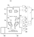
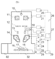
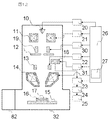
- FIG. 4 shows a configuration diagram of the electron microscope in the present embodiment.
- the electron microscope includes an electron optical system, a stage system, a control system, an image processing system, an operation interface 27, a sample chamber 32, and an exhaust chamber 82.
- the electron optical system includes an electron source 10, a condenser lens 11, a diaphragm 12, a deflector 13, an objective lens 14, and a detector 18.
- the stage system includes a sample stage 15, a sample holder 16, and a sample 17.
- the control system includes an electron source control unit 20, a condenser lens control unit 21, a deflection signal control unit 22, a detector control unit 31, and an SEM control unit 26.
- the image processing system includes a detection signal processing unit 23, an image generation unit 24, and an image display unit 25.
- the irradiation conditions controlled in this embodiment are the acceleration voltage of primary electrons, the irradiation current, and the scanning speed of primary electrons.
- the acceleration voltage is controlled by the voltage applied to the electron source 10 by the electron source control unit 20, and the irradiation current is controlled by the excitation current applied to the condenser lens 11 by the condenser lens control unit 21.
- the scanning speed is controlled by the deflection signal control unit 22 using a deflection signal to the deflector 13.
- FIG. 5B shows an SEM image acquired at an acceleration voltage of 1.0 ⁇ kV, an irradiation current of 8 ⁇ pA, and a primary electron scanning speed of 300 nm / ⁇ s.
- a in FIG. 5B is an SEM image of Sample 2 to which no ionic liquid is applied. The pattern portion becomes dark due to charging, and shading occurs.
- B in FIG. 5B is an SEM image of an observation specimen in which an ionic liquid is dropped on the sample 2 with a micropipette. When applied with a micropipette, the ionic liquid is not in the form of a thin film, and the primary electrons cannot pass through the ionic liquid, so the pattern cannot be identified.
- C in FIG. 5B is an SEM image of an observation specimen in which the ionic liquid on the sample 2 is a thin film. Shading of the pattern portion is suppressed and the pattern can be identified.
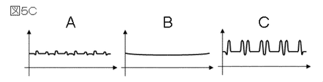
- FIG. 5C is a profile of image brightness analyzed in the direction across the groove pattern.
- the portion where the image brightness is maximum corresponds to the edge portion of the groove.
- the signal at the maximum corresponding to the edge portion is weak and the edge contrast is small.
- the profile of the edge portion cannot be identified.
- C in FIG. 5C has a strong local maximum signal and a clear edge contrast.
- the edge contrast representing the sample shape can be improved using an observation specimen in which the ionic liquid on the sample is a thin film.
- an electron microscopic method for measuring the film thickness of an ionic liquid and controlling the irradiation conditions of primary electrons based on the measured film thickness will be described.
- an observation specimen of C in FIG. 5A shown in Example 1 in which the ionic liquid on the sample is in the form of a thin film was used.
- the irradiation conditions of primary electrons are controlled in consideration of the film thickness of the ionic liquid and the range of primary electrons with low acceleration.
- the range of electrons indicates the length of passage through the substance.
- the range R ( ⁇ m) of the primary electrons is expressed by the following equation (1).
- Equation 1 indicates that the range of the primary electrons depends on the density and atomic weight of the substance in addition to the acceleration voltage of the primary electrons.
- the thickness of one molecular layer of the ionic liquid depends on the density and molecular weight of the ionic liquid, the thickness of one molecular layer (hereinafter, the thickness of one molecular layer is expressed as one monolayer) is a unit. As a result, the range of primary electrons can be defined by a monolayer.
- Acceleration voltage of primary electrons is, for example, in the range of 0.1 kV to 1.5 kV.
- the acceleration voltage of primary electrons that pass through a film thickness of 100 monolayers is 1.5 kV
- the acceleration voltage of primary electrons that pass through the thickness of one monolayer is 0.1 kV.
- one monolayer of a typical ionic liquid was 1 nm.
- the film thickness of the portion of the observation specimen to which the liquid medium containing the ionic liquid is applied is, for example, 1 monolayer or more and 100 monolayer or less.
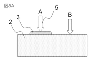
- FIG. 3A shows sample 2 and an observation specimen in which the ionic liquid on sample 2 is in a thin film form.
- the sample 2 is an insulator.
- FIG. 3B shows a time change of the secondary electron signal emitted when the sample 2 and the observation specimen in which the ionic liquid on the sample 2 is in the form of a thin film are irradiated with the low-acceleration primary electrons. As shown in B of FIG. 3B, when the sample 2 is irradiated with low-acceleration primary electrons, more secondary electrons are emitted than the number of irradiated primary electrons, and the sample surface is positively charged.
- Image and image brightness profile of sample 2 with pattern, observation target with ionic liquid on sample 2, and observation target with thin ionic liquid on sample 2 observed with primary electrons are shown in A, B and C of FIG.
- a in FIG. 5B when there is no ionic liquid, the pattern portion has a low contrast due to surface charging.
- B of FIG. 5B when the ionic liquid is not a thin film, the pattern portion is buried in the ionic liquid, and the edge contrast is lost.
- C in FIG. 5B when the ionic liquid is in a thin film shape, high contrast is obtained from the pattern portion. Further, as indicated by A in FIG.
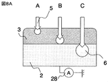
- FIG. 6 shows a configuration diagram of the electron microscope in this example.
- the electron microscope includes an electron optical system, a stage system, a control system, an image processing system, an operation interface 27, a sample chamber 32, an exhaust chamber 82, and a substrate current measurement system.
- the substrate current is a current that flows from the observation specimen to the stage system (sample holder 16) by the irradiation of primary electrons.
- the electron optical system includes an electron source 10, a condenser lens 11, a diaphragm 12, a deflector 13, an objective lens 14, and a detector 18.
- the stage system includes a sample stage 15, a sample holder 16, and a sample 17.
- the control system includes an electron source control unit 20, a condenser lens control unit 21, a deflection signal control unit 22, a detector control unit 31, and an SEM control unit 26.
- the image processing system includes a detection signal processing unit 23, an image generation unit 24, and an image display unit 25.
- the substrate current measurement system includes an ammeter 28 and a substrate current analysis unit 29.
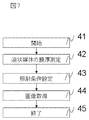
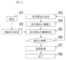
- Fig. 7 shows a flowchart of the electron microscopic method.
- the electron microscopic method in the present embodiment will be described with reference to the flowchart of FIG.
- the film thickness of the ionic liquid of the observation specimen is measured (step 42).
- the substrate current under primary electron irradiation was measured using the electron microscope shown in FIG. 6, and the film thickness of the ionic liquid was analyzed.
- the displacement current induced by the charge accumulated in the sample under primary electron irradiation can be measured as the substrate current.
- the electron source controller 20 controls the voltage applied to the electron source 10 to change the acceleration voltage of primary electrons, and the substrate current at each acceleration voltage is measured by the ammeter 28.
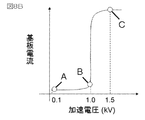
- FIG. 8A is a schematic diagram showing the relationship between the acceleration voltage of primary electrons and the range.
- the acceleration voltage of A, B, C and primary electrons is increased, the range of primary electrons 5 becomes longer.
- the range of primary electrons is equal to or greater than the film thickness of the ionic liquid 3 (C in FIG. 8A)
- the primary electrons reach the sample 2 and charges are accumulated in the sample.
- a displacement current is generated due to charge accumulation and can be measured as a substrate current.
- FIG. 8B shows changes in the substrate current when the acceleration voltage of the primary electrons is changed from 0.1 to 1.5 kV. It can be seen from FIG. 8B that the substrate current increases rapidly at an acceleration voltage of 1.0 kV.
- the acceleration voltage when the substrate current increases abruptly is the acceleration voltage when the primary electrons pass through the film thickness.
- the film thickness of the ionic liquid is 60 monolayers.
- the step of analyzing the acceleration voltage dependence of the substrate current described in the present embodiment is processed by the substrate current analysis unit 29, and the film thickness can be obtained automatically.
- the irradiation conditions of the primary electrons based on the film thickness are controlled (step 43).
- the acceleration voltage was controlled to 1.2 KV so that the range of primary electrons was longer than that of 60 monolayers.
- the primary electrons pass through the ionic liquid thin film and reach the sample. Therefore, in consideration of sample damage, the irradiation current was controlled to 5 ⁇ pA and the scanning speed was controlled to 300 ⁇ m / ⁇ s in order to limit the number of electrons irradiated to the sample.
- an image is acquired under the set irradiation conditions of the primary electrons, and the image is displayed on the image display unit 25 (step 44).
- FIG. 19 shows a graphical user interface (hereinafter referred to as GUI) for setting the irradiation conditions of the primary electrons in this embodiment.
- GUI graphical user interface
- the GUI of FIG. 19 is displayed on the monitor of the operation interface 27.
- information on the sample and ionic liquid input to the SEM control unit 26 is displayed.
- the window 131 displays the acceleration voltage dependency of the substrate current of the observation specimen and the film thickness of the ionic liquid.
- the window 132 displays the irradiation conditions of primary electrons according to the film thickness of the ionic liquid.
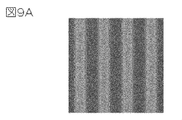
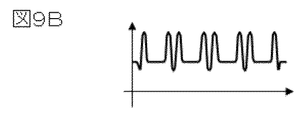
- FIG. 9A shows an image obtained by observing the observation specimen according to this example
- FIG. 9B shows an image brightness profile obtained by analyzing the image across the groove pattern.
- the maximum value of the image brightness representing the edge portion of the pattern is large, and a clear edge contrast can be obtained.
- the film thickness of the ionic liquid thin film can be measured and the optimum irradiation condition can be set, so that the edge contrast representing the sample shape can be improved.
- FIG. 10 shows a configuration diagram of an observation specimen preparation apparatus for an electron microscopic method in the present example.
- the observation specimen preparation device is an apparatus that applies an ionic liquid to a sample to produce an observation specimen.
- the exhaust chamber 82 and a control system are included.
- the control system includes an ionic liquid adjustment control unit 84, a discharge control unit 85, a rotation control unit 86, and an exhaust control unit 87.
- the observation specimen preparation apparatus of the present electron microscopic method is a part of the electron microscope, but may be independent of the electron microscope.
- the electron microscope in the present embodiment has the same configuration as that in FIG.
- Fig. 11 shows a flowchart of the electron microscopic method.
- the electron microscopic method in the present embodiment will be described with reference to the flowchart of FIG.
- an ionic liquid is applied to the sample 74 (step 52).
- the ionic liquid was applied using the observation specimen preparation device shown in FIG.
- the ionic liquid adjusted by the ionic liquid adjusting unit 72 is controlled by the discharge control unit 85 to be discharged from the discharge unit 73, and the ionic liquid is applied to the sample 74.
- pure water was mixed with the ionic liquid as a solvent, and the ionic liquid having a viscosity of 20 ⁇ mPa ⁇ s was discharged onto the sample.
- the applied ionic liquid is thinned based on the flowchart of FIG. 11 (step 53).
- the ionic liquid was thinned by using the observation specimen preparation apparatus of FIG.
- the sample holder 76 was rotated by the sample holder rotating mechanism 77.
- the rotation speed and rotation time were controlled by the rotation controller 86 so that the rotation speed and rotation time were rotated at 500 rpm for 10 seconds and then rotated at 3000 rpm for 60 seconds.
- the sample 74 was put into the exhaust chamber 82 and evacuated. If a substance that evaporates under vacuum is contained in the ionic liquid, the substance that evaporates under vacuum is evaporated by evacuation, so that the ionic liquid can be thinned.
- the vacuum evacuation was performed until the pressure in the exhaust chamber 82 became 1 ⁇ 10 ⁇ 4 Pa, which is the same degree of vacuum as that observed in the electron microscope.
- the evacuation is performed after the ionic liquid is applied, but the thinning process may be performed by applying the ionic liquid under vacuum.
- an image of the observation target is acquired based on the flowchart of FIG. 11 (step 54).
- the acceleration voltage of the primary electrons is 0.1 kV
- the soot current is 5 pA
- the scan speed is 200 nm / ⁇ s.
- the image obtained by observing the produced observation specimen is the same as C in FIG. 5B, and the profile of the image brightness analyzed in the direction crossing the groove pattern is the same as C in FIG. 5C.
- the maximum value of the image brightness representing the edge portion of the pattern is large, and a clear edge contrast can be obtained.
- the film thickness of the ionic liquid thin film can be controlled and an image can be acquired, so that the edge contrast representing the sample shape can be improved.
- FIG. 12 shows a configuration diagram of the electron microscope in this example.
- the electron microscope includes an electron optical system, a stage system, a control system, an image processing system, an operation interface 27, a sample chamber 32, and an exhaust chamber 82.
- the electron optical system includes an electron source 10, a condenser lens 11, a diaphragm 12, a deflector 13, an objective lens 14, a detector 18, and a pulse forming unit 19.
- the stage system includes a sample stage 15, a sample holder 16, and a sample 17.
- the control system includes an electron source control unit 20, a condenser lens control unit 21, a deflection signal control unit 22, a detector control unit 31, an SEM control unit 26, and a pulse control unit 30.
- the image processing system includes a detection signal processing unit 23, an image generation unit 24, and an image display unit 25.
- Fig. 13 shows a flowchart of the electron microscopic method.
- the electron microscopic method in the present embodiment will be described with reference to the flowchart of FIG.
- primary electron irradiation conditions are set (step 62).
- electron microscopy is performed using the electron microscope of FIG.
- the irradiation conditions of the primary electrons were set to an acceleration voltage of 0.3 kV with a high secondary electron emission rate.
- the film thickness of the ionic liquid is larger than the range of the primary electron of 0.3 keV, and the film of the ionic liquid is the surface of the sample. Thin film to reflect the shape.
- the irradiation conditions of the primary electrons with a high SN of the image, ie, the irradiation current of 20 ⁇ pA and the scanning speed of 100 nm / ⁇ s were controlled.
- the film thickness of the ionic liquid of the observation specimen was measured (step 65).
- the observation specimen used in this example is the observation specimen described in Example 3.
- the film thickness of the ionic liquid was analyzed by measuring the secondary electron emission rate using pulsed electrons using the electron microscope of FIG.
- a method for measuring the secondary electron emission rate will be described.
- the secondary electrons detected by the detector 18 are irradiated with the pulsed electrons formed by the pulse forming unit 19, and the secondary electron signal intensity decreases when the primary electrons are irradiated. This corresponds to a release rate of 1. If the intensity of the secondary electron signal when irradiated with the primary electrons is expressed by the intensity of the secondary electron signal in the steady state, the secondary electron emission rate can be obtained.
- FIG. 14 shows the acceleration voltage dependence of the secondary electron emission rate of the observation specimen used in this example.
- the dependence of the secondary electron emission rate of the ionic liquid and the resist on the acceleration voltage is compiled into a database. did.
- the acceleration voltage dependency 91 of the secondary electron emission rate of the resist called from the database and the acceleration voltage dependency 92 of the secondary electron emission rate of the ionic liquid are shown. Indicated.
- the secondary electron emission rate of the observed specimen is the same as the secondary electron emission rate 92 of the ionic liquid at an acceleration voltage of 0.8 ⁇ kV or less, and at the acceleration voltage of 1.5 kV or more, the secondary electron emission rate 91 of the resist is almost the same. Matched. On the other hand, at an accelerating voltage in the range of 0.8 to 1.5 kV, an intermediate value between the secondary electron emission rate 92 of the ionic liquid and the secondary electron emission rate 91 of the resist is obtained. Therefore, it can be determined from FIG. 14 that the ionic liquid has been transmitted when the acceleration voltage is 0.8 KV.
- the film thickness of the ionic liquid is 50 monolayers.
- the ionic liquid used in this example has one monolayer of 0.5 nm.
- step 66 it was determined whether the film thickness of the ionic liquid was appropriate (step 66).
- the range at an acceleration voltage of 0.3 kV in this example is 20 monolayers, which is equal to or less than the film thickness (50 monolayers) measured in this example.
- the application of the ionic liquid, the thinning process and the film thickness measurement are performed again (steps 63, 64, 65), and the process is repeated until the predetermined film thickness is obtained.
- Step 67 an image is acquired under the set irradiation conditions of the primary electrons, and the image is displayed on the image display unit 25.
- an image obtained by observing the produced observation specimen is the same as that in FIG. 9A, and the profile of the image brightness analyzed in the direction crossing the groove pattern is the same as that in FIG. 9B.
- the maximum value of the image brightness representing the edge portion of the pattern is large, and a clear edge contrast can be obtained.
- the edge contrast reflecting the sample shape can be improved.
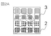
- FIG. 2A shows a top view of an observation target in which the ionic liquid has a retinal shape
- FIG. 2B shows a cross-sectional view of the observation target in which the ionic liquid has a retinal shape.
- an electron microscopic method using an observation specimen in which the ionic liquid is retinal as shown in FIG. 2 will be described.
- the configuration of the electron microscope shown in FIG. 12 was used.
- a SiO2 sample having a groove pattern having a different pitch and size was used.
- a hydrophobic ionic liquid was used and applied onto the pattern surface of the sample with a dip coater. Since the wettability of the ionic liquid and the sample differs according to the pattern pitch and pattern size of the sample, the state of the ionic liquid film differs for each pattern.
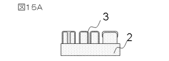
- FIG. 15A The structure of the observation target used in this example is shown in FIG. 15A.
- FIG. 15A in this observation specimen, the state of the ionic liquid film differs according to the pattern pitch and pattern size of the sample.
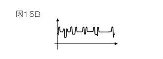
- FIG. 15B shows an image brightness profile obtained by analyzing the observed specimen with an acceleration voltage of 1.0 ⁇ kV, an irradiation current of 8 ⁇ pA, and a scanning speed of 300 ⁇ m / ⁇ s in a direction crossing the groove pattern.
- the contrast is in accordance with the pattern pitch and pattern size of the sample.
- the shape of the sample can be measured with high accuracy from an observation specimen having an ionic liquid.
- Example 3 a configuration different from the method described in Example 3 will be described for an observation specimen preparation apparatus for electron microscopy.
- FIG. 16 shows a configuration diagram of an electron microscope observation specimen preparation apparatus according to the present embodiment.
- An electron microscope observation specimen preparation apparatus includes a sample 101, a sample support unit 102 that supports the sample, a drive unit 103 that freely moves the sample support unit 102 up and down, and a drive control that controls the position and moving speed of the sample support unit 102.
- Part 104 an ionic liquid adjusting unit 106 that fills the liquid tank 108 with an ionic liquid 105 mixed with an ionic liquid or a substance other than the ionic liquid, and controls the adjustment of the ionic liquid 105 mixed with an ionic liquid or a substance other than the ionic liquid.
- the ionic liquid adjustment control unit 107 is configured.
- the configuration of the electron microscope observation specimen preparation apparatus may be a configuration installed in a sample chamber or an exhaust chamber of an electron microscope.
- sample 101 is a SiO2 sample having a linear groove pattern
- ionic liquid 105 is 1-Butyl-3-methylimidazolium bis (trifluoromethylsulfonyl) imide (1-ethyl-) containing 95% pure water. 3-methylimidazolium bis (trifluoromethanesulfonyl) imide).
- the ionic liquid 105 is applied to the sample 101 by pulling up the sample support unit 102 while controlling the moving speed of the drive unit 103 by the drive control unit 104.
- the film thickness of the ionic liquid 105 can be controlled.
- the speed at which the sample support 102 was pulled up from the liquid tank 108 was controlled to 5 cm / min, and the sample was applied onto the thin film.
- the sample 101 was placed in the exhaust chamber and evacuated. By evacuation, pure water contained in the ionic liquid can be evaporated to make the ionic liquid into a thin film. In this example, vacuum evacuation was performed until the pressure in the exhaust chamber became 2 ⁇ 10 ⁇ 2 Pa.
- the film thickness of the ionic liquid 105 formed on the sample 101 was found to be 100 monolayers by the film thickness measurement method of Example 2. If the observation specimen preparation apparatus of the electron microscope method of a present Example is used, the film thickness of the ionic liquid on a sample can be controlled with high precision.
- Example 3 a configuration different from the method described in Example 3 will be described for an observation specimen preparation apparatus for electron microscopy.
- FIG. 17 shows a configuration diagram of an electron microscope observation specimen preparation apparatus in this example.
- An electron microscopic observation specimen preparation apparatus includes a sample 111, a sample support unit 112 that supports the sample 111, a heater 113, a temperature control unit 114, an ionic liquid film 115, a film support unit 116 that supports the ionic liquid film 115, and a film support.
- the drive unit 117 is configured to move the unit 116, and the drive control unit 118.
- the ionic liquid film is a plate-like or film-like ionic liquid.
- the configuration of the electron microscope observation specimen preparation device may be a configuration installed in a sample holder, a sample chamber, or an exhaust chamber of an electron microscope.
- the sample 111 is a SiO2 sample having a pattern in which grooves are linearly formed.
- the sample 111 is supported on the sample support unit 112, and the film support unit 116 is lowered while controlling the moving speed of the drive unit 117 by the drive control unit 118, and the ionic liquid film 115 is brought into close contact with the sample 111.
- the temperature controller 114 controls the temperature of the heater 113 according to the type of the sample 111 and the type of the ionic liquid film 115, and the ionic liquid is applied to the sample 111. Since the viscosity of the ionic liquid decreases at a high temperature, it can be applied to the sample.
- the ionic liquid was applied to the sample 111 while the heater temperature was controlled to 60 ° C. while the ionic liquid film 115 was in close contact with the sample 111.
- the film thickness of the formed ionic liquid on the sample 111 was found to be one monolayer by the film thickness measurement method of Example 2. If the observation specimen preparation apparatus of the electron microscopic method of a present Example is used, the film thickness of the ionic liquid of an observation specimen can be controlled with high precision by temperature control of a heater.
- FIG. 18 shows a configuration diagram of an observation specimen preparation apparatus for an electron microscopic method in the present embodiment.
- An electron microscopic observation specimen preparation apparatus includes a sample 121, a sample support unit 122 that supports the sample, an ozone irradiation source 123, an ozone irradiation source control unit 124, an ionic liquid discharge unit 125, a discharge control unit 126, and an ionic liquid discharge unit 125.
- the ionic liquid adjustment control unit 140, the valve 141, the exhaust mechanism 142, the exhaust chamber 143, the exhaust control unit 144, the heater 145, and the temperature control unit 146 are configured.
- the configuration of the electron microscope observation specimen preparation apparatus may be a configuration installed in a sample chamber or an exhaust chamber of an electron microscope.
- an ionic liquid prepared by previously mixing an ionic liquid or a substance other than the ionic liquid with the ionic liquid adjusting unit 140 is prepared.
- the sample 121 is a SiO2 sample having a linear groove pattern
- pure water is added to 1-Butyl-3-methylimidazolium Tetrafluoroborate (1-butyl-3-methylimidazolium tetrafluoroborate).
- 1-Butyl-3-methylimidazolium Tetrafluoroborate 1-butyl-3-methylimidazolium tetrafluoroborate
- the ozone irradiation source control unit 124 controls the irradiation conditions of the ozone irradiation source 123 according to the types of the sample 121 and the ionic liquid, and the sample 121 supported by the sample support unit 122 is irradiated with ozone.
- Irradiated ozone modifies the surface state on the sample 121, so that the wettability with the liquid changes.
- the sample 121 was irradiated with ozone for 1 s.
- the discharge controller 126 controls the discharge amount of the ionic liquid and applies the ionic liquid.
- the ionic liquid was ejected by an ink jet method.
- the piezo method instead of the thermal method.
- the discharge amount per discharge of the ionic liquid depends on the nozzle diameter and applied voltage, and can be controlled in the range of fl to ⁇ l. In this embodiment, 2 pl was set for each discharge.
- the drive control unit 128 controls the drive mechanism 127 to move the ionic liquid discharge unit 125 to apply the ionic liquid.
- the temperature control unit 146 controls the temperature of the heater 145 according to the type of sample, the type of ionic liquid and the discharge amount, and the temperature of the sample 121 is adjusted. adjust. Since the wettability between the sample and the ionic liquid changes by adjusting the temperature of the sample 121, the form of the applied ionic liquid can create an advantageous state for thinning. In this example, the temperature of the sample 121 when applying the ionic liquid was set to 40 ° C. Thereafter, the exhaust control unit 144 controls the exhaust mechanism 142 to evacuate the exhaust chamber 143.
- the substance that evaporates under vacuum is evaporated by evacuation, so that the ionic liquid can be thinned.
- the vacuum chamber was evacuated until the pressure in the exhaust chamber 143 reached 1 ⁇ 10 ⁇ 4 Pa, which is the same degree of vacuum as observed with an electron microscope, and pure water was evaporated.
- the observation specimen is controlled by controlling the irradiation conditions of ozone, adjusting the ionic liquid, controlling the discharge amount of the ionic liquid, controlling the temperature of the sample, and controlling the evacuation.
- the film thickness of the body ionic liquid can be controlled with high accuracy.
- ozone is irradiated, but ultraviolet light or plasma may be irradiated.
Landscapes
- Analytical Chemistry (AREA)
- Chemical & Material Sciences (AREA)
- Physics & Mathematics (AREA)
- General Physics & Mathematics (AREA)
- Life Sciences & Earth Sciences (AREA)
- Health & Medical Sciences (AREA)
- Electromagnetism (AREA)
- Biochemistry (AREA)
- General Health & Medical Sciences (AREA)
- Immunology (AREA)
- Pathology (AREA)
- Analysing Materials By The Use Of Radiation (AREA)
- Length-Measuring Devices Using Wave Or Particle Radiation (AREA)
- Sampling And Sample Adjustment (AREA)
Priority Applications (3)
| Application Number | Priority Date | Filing Date | Title |
|---|---|---|---|
| CN201280051975.6A CN103907004B (zh) | 2011-11-02 | 2012-10-16 | 电子显微法的观察样品、电子显微法、电子显微镜以及观察样品制作装置 |
| US14/354,917 US9202668B2 (en) | 2011-11-02 | 2012-10-16 | Observation specimen for use in electron microscopy, electron microscopy, electron microscope, and device for producing observation specimen |
| DE112012004204.2T DE112012004204B4 (de) | 2011-11-02 | 2012-10-16 | Elektronenmikroskopisches Verfahren und Elektronenmikroskop |
Applications Claiming Priority (2)
| Application Number | Priority Date | Filing Date | Title |
|---|---|---|---|
| JP2011241040A JP5951223B2 (ja) | 2011-11-02 | 2011-11-02 | 電子顕微法、電子顕微鏡および観察標体作製装置 |
| JP2011-241040 | 2011-11-02 |
Publications (1)
| Publication Number | Publication Date |
|---|---|
| WO2013065475A1 true WO2013065475A1 (ja) | 2013-05-10 |
Family
ID=48191832
Family Applications (1)
| Application Number | Title | Priority Date | Filing Date |
|---|---|---|---|
| PCT/JP2012/076704 Ceased WO2013065475A1 (ja) | 2011-11-02 | 2012-10-16 | 電子顕微法の観察標体、電子顕微法、電子顕微鏡および観察標体作製装置 |
Country Status (5)
| Country | Link |
|---|---|
| US (1) | US9202668B2 (enExample) |
| JP (1) | JP5951223B2 (enExample) |
| CN (1) | CN103907004B (enExample) |
| DE (1) | DE112012004204B4 (enExample) |
| WO (1) | WO2013065475A1 (enExample) |
Families Citing this family (7)
| Publication number | Priority date | Publication date | Assignee | Title |
|---|---|---|---|---|
| JP5723801B2 (ja) | 2012-02-06 | 2015-05-27 | 株式会社日立ハイテクノロジーズ | 荷電粒子線装置および配線方法 |
| US9086343B2 (en) * | 2012-03-09 | 2015-07-21 | Hitachi High-Technologies Corporation | Methods for observing samples and preprocessing thereof |
| EP3062082B1 (en) * | 2015-02-25 | 2018-04-18 | Fei Company | Preparation of sample for charged-particle microscopy |
| JP6357583B2 (ja) * | 2015-04-24 | 2018-07-11 | 株式会社日立ハイテクノロジーズ | イオン液体を用いた試料の観察方法及び標本の生産方法 |
| US9633816B2 (en) * | 2015-05-18 | 2017-04-25 | Fei Company | Electron beam microscope with improved imaging gas and method of use |
| TWI594288B (zh) * | 2016-03-14 | 2017-08-01 | 台灣電鏡儀器股份有限公司 | 電子顯微鏡 |
| CN107608141B (zh) * | 2017-09-13 | 2020-10-09 | 深圳市华星光电半导体显示技术有限公司 | 显示面板及其制备方法、显示装置 |
Citations (2)
| Publication number | Priority date | Publication date | Assignee | Title |
|---|---|---|---|---|
| JP2000338017A (ja) * | 1999-05-27 | 2000-12-08 | Canon Inc | 走査電子顕微鏡観察用試料の前処理装置及び前処理方法 |
| WO2007083756A1 (ja) * | 2006-01-20 | 2007-07-26 | Juridical Foundation Osaka Industrial Promotion Organization | 電子顕微鏡用チャージアップ防止液状媒体、及びそれを用いた試料観察方法 |
Family Cites Families (10)
| Publication number | Priority date | Publication date | Assignee | Title |
|---|---|---|---|---|
| JP2000195459A (ja) | 1998-12-24 | 2000-07-14 | Canon Inc | 試料観察方法および走査型電子顕微鏡 |
| CN100360708C (zh) * | 2004-05-12 | 2008-01-09 | 中国科学院金属研究所 | 透射电镜用薄膜样品的制备方法 |
| JP5474312B2 (ja) * | 2007-06-20 | 2014-04-16 | 株式会社日立ハイテクノロジーズ | 荷電粒子ビーム装置及びその制御方法 |
| CN101458180B (zh) * | 2007-12-13 | 2011-10-05 | 中芯国际集成电路制造(上海)有限公司 | 预处理tem样品以及对样品进行tem测试的方法 |
| JP5226378B2 (ja) * | 2008-04-28 | 2013-07-03 | 株式会社日立ハイテクノロジーズ | 透過型電子顕微鏡、及び試料観察方法 |
| JP2010025656A (ja) * | 2008-07-17 | 2010-02-04 | Jeol Ltd | イオン液体を用いた試料の処理方法及び処理システム |
| JP2010118564A (ja) * | 2008-11-14 | 2010-05-27 | Hitachi High-Technologies Corp | パターンの検査装置、およびパターンの検査方法 |
| CN101776543A (zh) * | 2009-01-13 | 2010-07-14 | 中芯国际集成电路制造(上海)有限公司 | 透射电子显微镜检测样片的制备方法 |
| JP5442417B2 (ja) * | 2009-12-14 | 2014-03-12 | 株式会社日立ハイテクノロジーズ | 荷電粒子線装置及び試料観察方法 |
| JP5707082B2 (ja) * | 2010-10-08 | 2015-04-22 | 株式会社日立ハイテクノロジーズ | 液体の表面を浮遊する試料の走査電子顕微鏡観察方法 |
-
2011
- 2011-11-02 JP JP2011241040A patent/JP5951223B2/ja active Active
-
2012
- 2012-10-16 WO PCT/JP2012/076704 patent/WO2013065475A1/ja not_active Ceased
- 2012-10-16 DE DE112012004204.2T patent/DE112012004204B4/de not_active Expired - Fee Related
- 2012-10-16 US US14/354,917 patent/US9202668B2/en active Active
- 2012-10-16 CN CN201280051975.6A patent/CN103907004B/zh not_active Expired - Fee Related
Patent Citations (2)
| Publication number | Priority date | Publication date | Assignee | Title |
|---|---|---|---|---|
| JP2000338017A (ja) * | 1999-05-27 | 2000-12-08 | Canon Inc | 走査電子顕微鏡観察用試料の前処理装置及び前処理方法 |
| WO2007083756A1 (ja) * | 2006-01-20 | 2007-07-26 | Juridical Foundation Osaka Industrial Promotion Organization | 電子顕微鏡用チャージアップ防止液状媒体、及びそれを用いた試料観察方法 |
Also Published As
| Publication number | Publication date |
|---|---|
| DE112012004204T5 (de) | 2014-09-11 |
| CN103907004B (zh) | 2016-10-26 |
| JP2013096890A (ja) | 2013-05-20 |
| US20140264018A1 (en) | 2014-09-18 |
| CN103907004A (zh) | 2014-07-02 |
| JP5951223B2 (ja) | 2016-07-13 |
| DE112012004204B4 (de) | 2020-08-13 |
| US9202668B2 (en) | 2015-12-01 |
Similar Documents
| Publication | Publication Date | Title |
|---|---|---|
| JP5951223B2 (ja) | 電子顕微法、電子顕微鏡および観察標体作製装置 | |
| TWI631343B (zh) | 檢測帶電荷試件表面的方法及裝置 | |
| US8698080B2 (en) | Scanning electron microscope | |
| JP2009099540A (ja) | 試料の検査,測定方法、及び走査電子顕微鏡 | |
| JP7149906B2 (ja) | 走査電子顕微鏡及びパタン計測方法 | |
| JP4500646B2 (ja) | 試料観察方法及び電子顕微鏡 | |
| US20180277333A1 (en) | Charged particle beam apparatus | |
| JP5406308B2 (ja) | 電子線を用いた試料観察方法及び電子顕微鏡 | |
| US11688583B2 (en) | Operating a particle beam apparatus with an object holder | |
| JP4089580B2 (ja) | 薄膜の厚さ及び厚さ分布の評価方法 | |
| JP2013096890A5 (enExample) | ||
| JP6433515B2 (ja) | ミラーイオン顕微鏡およびイオンビーム制御方法 | |
| JP5074262B2 (ja) | 帯電電位測定方法、及び荷電粒子顕微鏡 | |
| US11011348B2 (en) | Scanning electron microscope and sample observation method using scanning electron microscope | |
| CN106373848B (zh) | 采用等离子体中和的电子显微镜装置 | |
| JPH08313244A (ja) | 薄膜の膜厚測定方法 | |
| JP2014022163A (ja) | 走査電子顕微鏡および試料の予備帯電条件設定方法 | |
| JP2013213747A (ja) | イオンビーム装置、試料観察方法、および試料作製装置 | |
| JP4658783B2 (ja) | 試料像形成方法 | |
| JP2009129799A (ja) | 走査透過型電子顕微鏡 | |
| US20140291509A1 (en) | Charged particle beam apparatus and method for forming observation image | |
| JP2014149921A (ja) | イオンビーム装置、および試料観察方法 | |
| JP5592136B2 (ja) | チップ先端構造検査方法 | |
| JPH0618636A (ja) | イオンビームを用いたデバイステスト方法およびテスタ | |
| Ohta et al. | Development of micro focus X-ray microscope equipped with high brightness Li/W< 111> field emitter |
Legal Events
| Date | Code | Title | Description |
|---|---|---|---|
| 121 | Ep: the epo has been informed by wipo that ep was designated in this application |
Ref document number: 12845750 Country of ref document: EP Kind code of ref document: A1 |
|
| WWE | Wipo information: entry into national phase |
Ref document number: 14354917 Country of ref document: US |
|
| WWE | Wipo information: entry into national phase |
Ref document number: 112012004204 Country of ref document: DE Ref document number: 1120120042042 Country of ref document: DE |
|
| 122 | Ep: pct application non-entry in european phase |
Ref document number: 12845750 Country of ref document: EP Kind code of ref document: A1 |