WO2013046955A1 - Memsセンサ - Google Patents
Memsセンサ Download PDFInfo
- Publication number
- WO2013046955A1 WO2013046955A1 PCT/JP2012/070420 JP2012070420W WO2013046955A1 WO 2013046955 A1 WO2013046955 A1 WO 2013046955A1 JP 2012070420 W JP2012070420 W JP 2012070420W WO 2013046955 A1 WO2013046955 A1 WO 2013046955A1
- Authority
- WO
- WIPO (PCT)
- Prior art keywords
- mems sensor
- sensor
- mems
- signal processing
- processing lsi
- Prior art date
- Legal status (The legal status is an assumption and is not a legal conclusion. Google has not performed a legal analysis and makes no representation as to the accuracy of the status listed.)
- Ceased
Links
Images

Classifications
-
- B—PERFORMING OPERATIONS; TRANSPORTING
- B81—MICROSTRUCTURAL TECHNOLOGY
- B81B—MICROSTRUCTURAL DEVICES OR SYSTEMS, e.g. MICROMECHANICAL DEVICES
- B81B3/00—Devices comprising flexible or deformable elements, e.g. comprising elastic tongues or membranes
- B81B3/0018—Structures acting upon the moving or flexible element for transforming energy into mechanical movement or vice versa, i.e. actuators, sensors, generators
-
- G—PHYSICS
- G01—MEASURING; TESTING
- G01C—MEASURING DISTANCES, LEVELS OR BEARINGS; SURVEYING; NAVIGATION; GYROSCOPIC INSTRUMENTS; PHOTOGRAMMETRY OR VIDEOGRAMMETRY
- G01C19/00—Gyroscopes; Turn-sensitive devices using vibrating masses; Turn-sensitive devices without moving masses; Measuring angular rate using gyroscopic effects
- G01C19/56—Turn-sensitive devices using vibrating masses, e.g. vibratory angular rate sensors based on Coriolis forces
- G01C19/5783—Mountings or housings not specific to any of the devices covered by groups G01C19/5607 - G01C19/5719
-
- B—PERFORMING OPERATIONS; TRANSPORTING
- B81—MICROSTRUCTURAL TECHNOLOGY
- B81B—MICROSTRUCTURAL DEVICES OR SYSTEMS, e.g. MICROMECHANICAL DEVICES
- B81B7/00—Microstructural systems ; Auxiliary parts of microstructural devices or systems
- B81B7/0083—Temperature control
-
- B—PERFORMING OPERATIONS; TRANSPORTING
- B81—MICROSTRUCTURAL TECHNOLOGY
- B81C—PROCESSES OR APPARATUS SPECIALLY ADAPTED FOR THE MANUFACTURE OR TREATMENT OF MICROSTRUCTURAL DEVICES OR SYSTEMS
- B81C1/00—Manufacture or treatment of devices or systems in or on a substrate
- B81C1/00015—Manufacture or treatment of devices or systems in or on a substrate for manufacturing microsystems
- B81C1/00222—Integrating an electronic processing unit with a micromechanical structure
- B81C1/00238—Joining a substrate with an electronic processing unit and a substrate with a micromechanical structure
-
- G—PHYSICS
- G01—MEASURING; TESTING
- G01P—MEASURING LINEAR OR ANGULAR SPEED, ACCELERATION, DECELERATION, OR SHOCK; INDICATING PRESENCE, ABSENCE, OR DIRECTION, OF MOVEMENT
- G01P15/00—Measuring acceleration; Measuring deceleration; Measuring shock, i.e. sudden change of acceleration
- G01P15/02—Measuring acceleration; Measuring deceleration; Measuring shock, i.e. sudden change of acceleration by making use of inertia forces using solid seismic masses
- G01P15/08—Measuring acceleration; Measuring deceleration; Measuring shock, i.e. sudden change of acceleration by making use of inertia forces using solid seismic masses with conversion into electric or magnetic values
- G01P15/0802—Details
-
- G—PHYSICS
- G01—MEASURING; TESTING
- G01P—MEASURING LINEAR OR ANGULAR SPEED, ACCELERATION, DECELERATION, OR SHOCK; INDICATING PRESENCE, ABSENCE, OR DIRECTION, OF MOVEMENT
- G01P21/00—Testing or calibrating of apparatus or devices covered by the preceding groups
-
- B—PERFORMING OPERATIONS; TRANSPORTING
- B81—MICROSTRUCTURAL TECHNOLOGY
- B81B—MICROSTRUCTURAL DEVICES OR SYSTEMS, e.g. MICROMECHANICAL DEVICES
- B81B2201/00—Specific applications of microelectromechanical systems
- B81B2201/02—Sensors
- B81B2201/0278—Temperature sensors
Definitions
- the present invention relates to the structure of a sensor, and more particularly to the structure of a MEMS sensor using MEMS technology.
- MEMS Micro Electro Mechanical Systems
- a sensor created by applying the MEMS technology that is, the MEMS sensor is a sensor created by using a semiconductor process, so that the output signal is often a very small output. Therefore, generally, a signal processing LSI is mounted in the subsequent stage.
- the manufacturing process of the MEMS sensor and the manufacturing process of the semiconductor have no affinity in the portion including deep etching, the handling of the sacrificial layer, etc. is also different. Since a problem also arises, the MEMS sensor chip and the signal processing LSI are often separate chips.
- a signal processing LSI is often stacked on a MEMS sensor chip.
- the MEMS sensor chip and the signal processing LSI chip stacked as in Patent Document 1 are bonded by an adhesive member such as an adhesive or an adhesive sheet.
- an adhesive member such as an adhesive or an adhesive sheet.
- the MEMS chip and the signal processing LSI chip are bonded to an arbitrary position, there is a possibility that a temperature gradient is generated on the MEMS chip depending on the position of the heat generating portion of the signal processing LSI.
- the temperature gradient on the MEMS chip has a temperature gradient in the sensing element, which may cause performance degradation due to the influence of temperature.
- the temperature sensor part for correcting the temperature characteristics of the sensor itself mounted on the signal processing LSI has a temperature gradient on the MEMS sensor element, the correction becomes difficult.
- An object of the present invention is to provide a MEMS sensor in which the influence of changes in temperature characteristics due to heat is reduced.
- a MEMS sensor of the present invention includes a signal processing LSI on which a temperature sensor for measuring a sensor temperature is mounted, and a MEMS sensor chip mounted on the signal processing LSI. And the MEMS sensor chip is mounted on the heat generating portion of the signal processing LSI.
- the top view of the MEMS sensor in a 1st Example The perspective view of the MEMS sensor in a 1st Example.
- the top view of the MEMS sensor in a 1st Example An example of the top view of a MEMS sensor.
- the top view of the MEMS sensor in a 2nd Example The top view of the MEMS sensor in a 3rd Example.
- the top view of the MEMS sensor in a 4th Example The top view of the MEMS sensor in a 5th Example.
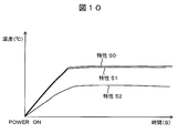
- the top view of the MEMS sensor in a 6th Example The figure which showed the temperature characteristic.
- the MEMS sensor chip is arranged immediately above the position where the heat generated when the signal processing LSI performs the signal processing operation is known in advance by simulation technology or the like.
- the performance of the sensor is improved by arranging so that the temperature gradient of the entire MEMS sensor element is minimized by the adjustment.
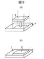
- Example 1 A first embodiment which is an embodiment of the present invention will be described with reference to FIGS.
- 1 is a signal processing LSI
- 2 is a MEMS sensor chip
- 3 is a temperature measurement unit
- 10 is a heat generation unit of the signal processing LSI 1.
- This sensor has the MEMS sensor chip 2 mounted on a signal processing LSI 1 as shown in FIG. 2 (a), and a bonding member (not shown) as shown in the perspective view of FIG. 2 (b). Fix it.
- the MEMS sensor chip 2 when the MEMS sensor chip 2 is arranged at an arbitrary position on the signal processing LSI 1, a part of the MEMS sensor chip 2 is heated by the heating unit 10, and heat nonuniformity is generated on the MEMS sensor chip 2.
- the temperature becomes non-uniform inside the sensor element.
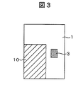
- the heat generating part 10 and the sensor chip 2 of the signal processing LSI 1 are arranged immediately above the heat generating part 10 as shown in FIG. Thereby, the temperature gradient inside the sensor element can be reduced.
- the positional relationship between the heat generating unit 10 of the signal processing LSI 1 and the temperature measuring unit 3 is not adjacent to the heat generating unit 10 as shown in FIG. 1, but between the heat generating unit 10 of the signal processing LSI 1 and the MEMS sensor chip 2.
- the thermal resistance of the signal processing LSI 1 and the thermal capacity of the sensor chip 2 are taken into consideration, and the thermal resistance and the thermal capacity are matched or their ratios are matched.
- the temperature gradient on the MEMS sensor chip 2 can be reduced, and the temperature characteristics at the time of transient can be corrected, and the influence of changes in temperature characteristics due to heat can be reduced.
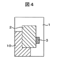
- Example 2 Next, a second embodiment, which is another embodiment, will be described with reference to FIG. Constituent elements similar to those described in FIGS.
- the heat generating part 10 and the other heat generating part 11 are on the signal processing LSI 1.
- another heat generating portion 11 is arranged in the vicinity of the heat generating portion 10 like the other heat generating portion 12 in the semiconductor layout as shown in FIG.
- the MEMS sensor chip 2 is disposed immediately above the heat generating unit 10 and the other heat generating unit 12.
- the heat generating part 10 and the other heat generating part 11 are made to be another heat generating part 12 whose shape is changed by the semiconductor layout, and the signal processing LSI 1 is changed.
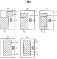
- the heat generating part may be arranged collectively in the central part, and the MEMS sensor chip 2 may be mounted as shown in FIG.
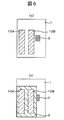
- the heat generating section 10 is divided into a plurality of parts (in this embodiment, it is divided into two as an example), and a temperature gradient is unlikely to occur in the sensor element on the MEMS sensor chip 2. As shown in FIG. 6A, the heat generating section 10 is divided into a plurality of parts (in this embodiment, it is divided into two as an example), and a temperature gradient is unlikely to occur in the sensor element on the MEMS sensor chip 2. As shown in FIG. 6A, the heat generating section 10 is divided into a plurality of parts (in this embodiment, it is divided into two as an example), and a temperature gradient is unlikely to occur in the sensor element on the MEMS sensor chip 2. As shown in FIG.
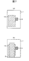
- the heat generating portion 10 of the signal processing LSI 1 has a shape as shown in FIG. It is assumed that the shape of the MEMS sensor chip 2 is a vertically long shape as compared with the heat generating portion 10 as shown in FIG. In the case of the present embodiment, the MEMS sensor chip 2 is arranged so that the temperature gradient is minimized in the sensor element on the MEMS sensor chip 2 as shown in FIG.
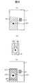
- the heat generating unit 10 and the temperature measuring unit 3 are arranged on the signal processing LSI 1 as shown in FIG.
- the heat generation amount per unit time in the heat generation unit 10 is integrated, and the center of the heat generation unit calculated from the integrated value and the area of the heat generation unit is 101.
- one MEMS sensor element 20 is mounted on the MEMS sensor chip 2 as shown in FIG.
- FIG. 8B it is assumed that the MEMS sensor element 20 is arranged on the MEMS sensor chip 2 and has a center 201 calculated from the area of the sensor portion of the MEMS sensor element 20.
- the temperature detection unit 3 on the signal processing LSI 1 measures the temperature at which the heat generated by the heat generation unit 10 is transferred on the signal processing LSI 1. Assuming that the temperature of the sensor part of the MEMS sensor element 20 has a time characteristic as shown by the characteristic 50, the detected temperature of the temperature detection part 3 has a thermal resistance, Arrange for heat capacity. Alternatively, an arrangement that is proportional to the characteristic 50 such as the characteristic 52 is adopted.
- Such a configuration makes it possible to reduce the influence of changes in temperature characteristics due to heat.
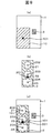
- the heat generating unit 10 and the temperature measuring unit 3 are arranged on the signal processing LSI 1 as shown in FIG.
- the heat generation amount per unit time in the heat generation unit 10 is integrated, and the center of the heat generation unit calculated from the integrated value and the area of the heat generation unit is 101.
- the MEMS sensor chip 2 has a plurality of MEMS sensor elements, and in this embodiment, there are three cases.
- the MEMS sensor element 21, the MEMS sensor element 22, and the MEMS sensor element 23 are arranged on the MEMS sensor chip 2, and the center calculated from the area of the sensor portion of each MEMS sensor element is the same as in the fifth embodiment.
- the center 202, the center 203, and the center 204 respectively.
- the center calculated comprehensively from the areas of these sensor portions is 201.
- the heat generating unit 10 is arranged as shown in FIG. 9C so that the center 101 of the heat generating part 10 and the center 201 calculated from the MEMS sensor element 21, the MEMS sensor element 22, and the MEMS sensor element 23 coincide.
- the heat transferred from the heat generating portion 10 of the signal processing LSI 1 is transmitted relatively uniformly to the sensor portions of the MEMS sensor element 21, MEMS sensor element 22, and MEMS sensor element 23 on the MEMS sensor chip 2. . Thereby, the characteristic can be stabilized.
- the temperature detection unit 3 on the signal processing LSI 1 measures the temperature at which the heat generated by the heat generation unit 10 is transferred on the signal processing LSI 1.
- the detected temperature of the temperature detection part 3 has a characteristic 51 depending on the layout of the semiconductor process. The heat resistance and heat capacity are taken into consideration so as to become like this. Alternatively, an arrangement that is proportional to the characteristic 50 such as the characteristic 52 is adopted.
- examples of the MEMS sensor of the present invention include a sensor that detects and processes an externally applied signal such as acceleration and angular velocity, but is not limited thereto. Further, the present invention can also be applied to a MEMS sensor in which an acceleration sensor and an angular velocity sensor are mounted in the same manner, or a biaxial acceleration sensor and an angular velocity sensor, in which a triaxial acceleration sensor and an angular velocity sensor are mounted in the same manner.
Landscapes
- Engineering & Computer Science (AREA)
- Physics & Mathematics (AREA)
- General Physics & Mathematics (AREA)
- Microelectronics & Electronic Packaging (AREA)
- Manufacturing & Machinery (AREA)
- Computer Hardware Design (AREA)
- Radar, Positioning & Navigation (AREA)
- Remote Sensing (AREA)
- Chemical & Material Sciences (AREA)
- Analytical Chemistry (AREA)
- Micromachines (AREA)
- Gyroscopes (AREA)
Abstract
Description
図1乃至図4を用いて本発明の一実施例である第1の実施例について説明する。
次に、他の一実施例である第2の実施例について図5を用いて説明する。図1乃至図4記載と同様の構成要素には同符号を付し説明を省略する。
次に、図6を用いて他の一実施例である第3の実施例について説明する。図1乃至図5記載と同様の構成要素には同符号を付し説明を省略する。
次に、図7を用いて他の一実施例である第4の実施例について説明する。図1乃至図6に記載と同様の構成要素には同符号を付して説明を省略する。
次に、図8を用いて他の一実施例である第5の実施例について説明する。図1乃至図7に記載と同様の構成要素には同符号を付して説明を省略する。
次に、図9を用いて他の一実施例である第6の実施例について説明する。図1乃至図8に記載と同様の構成要素には同符号を付して説明を省略する。
2 MEMSセンサチップ
3 温度検出部
10、11、12 発熱部
20、21、22、23 MEMSセンサエレメント
101 発熱部の中心
201、202、203、204 MEMSセンサエレメントの中心
本明細書で引用した全ての刊行物、特許および特許出願をそのまま参考として本明細書にとり入れるものとする。
Claims (8)
- センサ温度を測定するための温度センサが搭載された信号処理用LSIと、
前記信号処理用LSI上に搭載されたMEMSセンサチップと、を有し、
前記MEMSセンサチップは前記信号処理用LSIの発熱部上に搭載したことを特徴とするMEMSセンサ。 - 請求項1に記載のMEMSセンサにおいて、
前記MEMSセンサチップは、加速度センサであることを特徴とするMEMSセンサ。 - 請求項1に記載のMEMSセンサにおいて、
前記MEMSセンサチップは、角速度センサであることを特徴とするMEMSセンサ。 - 請求項1に記載のMEMSセンサにおいて、
前記MEMSセンサチップは、加速度センサと角速度センサからなることを特徴とするMEMSセンサ。 - 請求項1に記載のMEMSセンサにおいて、
前記MEMSセンサチップは、2軸の加速度センサと角速度センサからなることを特徴とするMEMSセンサ。 - 請求項1に記載のMEMSセンサにおいて、
前記MEMSセンサチップは、3軸の加速度センサと角速度センサからなることを特徴とするMEMSセンサ。 - 請求項1に記載のMEMSセンサにおいて、
前記信号処理用LSIの発熱部と前記MEMSセンサのセンシング部との間の持つ熱抵抗、熱容量と同等の熱抵抗、熱容量を持つ位置に前記温度センサを配置したことを特徴とするMEMSセンサ。 - 請求項1に記載のMEMSセンサにおいて、
前記信号処理用LSIの発熱部とMEMSセンサのセンシング部との間の持つ熱抵抗、熱容量とそれぞれ同一の比の熱抵抗、熱容量を持つ位置に前記温度センサ部を配置することを特徴とするMEMSセンサ。
Priority Applications (2)
| Application Number | Priority Date | Filing Date | Title |
|---|---|---|---|
| DE112012004062.7T DE112012004062T5 (de) | 2011-09-30 | 2012-08-10 | MEMS-Sensor |
| US14/239,877 US20140191342A1 (en) | 2011-09-30 | 2012-08-10 | Mems sensor |
Applications Claiming Priority (2)
| Application Number | Priority Date | Filing Date | Title |
|---|---|---|---|
| JP2011-215901 | 2011-09-30 | ||
| JP2011215901A JP5723739B2 (ja) | 2011-09-30 | 2011-09-30 | Memsセンサ |
Publications (1)
| Publication Number | Publication Date |
|---|---|
| WO2013046955A1 true WO2013046955A1 (ja) | 2013-04-04 |
Family
ID=47995007
Family Applications (1)
| Application Number | Title | Priority Date | Filing Date |
|---|---|---|---|
| PCT/JP2012/070420 Ceased WO2013046955A1 (ja) | 2011-09-30 | 2012-08-10 | Memsセンサ |
Country Status (4)
| Country | Link |
|---|---|
| US (1) | US20140191342A1 (ja) |
| JP (1) | JP5723739B2 (ja) |
| DE (1) | DE112012004062T5 (ja) |
| WO (1) | WO2013046955A1 (ja) |
Families Citing this family (2)
| Publication number | Priority date | Publication date | Assignee | Title |
|---|---|---|---|---|
| JP6313452B2 (ja) | 2015-04-20 | 2018-04-18 | エスゼット ディージェイアイ テクノロジー カンパニー リミテッドSz Dji Technology Co.,Ltd | センサ動作を熱的に調節するシステム、方法および無人航空機 |
| US10525945B2 (en) * | 2017-04-18 | 2020-01-07 | Goodrich Corporation | Antiskid brake control system with axle-mounted inertial sensor |
Citations (2)
| Publication number | Priority date | Publication date | Assignee | Title |
|---|---|---|---|---|
| JPH1010148A (ja) * | 1996-06-25 | 1998-01-16 | Japan Aviation Electron Ind Ltd | 半導体姿勢センシングチップ |
| JP2009053100A (ja) * | 2007-08-28 | 2009-03-12 | Mitsutoyo Corp | Memsモジュール及びmemsモジュールの特性安定化方法 |
Family Cites Families (8)
| Publication number | Priority date | Publication date | Assignee | Title |
|---|---|---|---|---|
| JPH0666568A (ja) * | 1992-08-19 | 1994-03-08 | Sumitomo Electric Ind Ltd | 角速度検出装置、方位検出装置および位置検出装置 |
| JP2002181550A (ja) * | 2000-10-02 | 2002-06-26 | Ngk Insulators Ltd | 角速度測定装置 |
| US7664573B2 (en) * | 2003-09-26 | 2010-02-16 | Siemens Industry, Inc. | Integrated building environment data system |
| JP2008203155A (ja) * | 2007-02-21 | 2008-09-04 | Denso Corp | センサ回路 |
| JP2010204038A (ja) * | 2009-03-05 | 2010-09-16 | Toyota Motor Corp | 角速度検出装置 |
| JP2010219243A (ja) * | 2009-03-16 | 2010-09-30 | Sanken Electric Co Ltd | 半導体モジュール及びその制御方法 |
| JP2011061132A (ja) * | 2009-09-14 | 2011-03-24 | Zycube:Kk | インターポーザ |
| JP2011128140A (ja) * | 2009-11-19 | 2011-06-30 | Dainippon Printing Co Ltd | センサデバイス及びその製造方法 |
-
2011
- 2011-09-30 JP JP2011215901A patent/JP5723739B2/ja not_active Expired - Fee Related
-
2012
- 2012-08-10 US US14/239,877 patent/US20140191342A1/en not_active Abandoned
- 2012-08-10 WO PCT/JP2012/070420 patent/WO2013046955A1/ja not_active Ceased
- 2012-08-10 DE DE112012004062.7T patent/DE112012004062T5/de not_active Ceased
Patent Citations (2)
| Publication number | Priority date | Publication date | Assignee | Title |
|---|---|---|---|---|
| JPH1010148A (ja) * | 1996-06-25 | 1998-01-16 | Japan Aviation Electron Ind Ltd | 半導体姿勢センシングチップ |
| JP2009053100A (ja) * | 2007-08-28 | 2009-03-12 | Mitsutoyo Corp | Memsモジュール及びmemsモジュールの特性安定化方法 |
Also Published As
| Publication number | Publication date |
|---|---|
| US20140191342A1 (en) | 2014-07-10 |
| JP2013076600A (ja) | 2013-04-25 |
| JP5723739B2 (ja) | 2015-05-27 |
| DE112012004062T5 (de) | 2014-07-10 |
Similar Documents
| Publication | Publication Date | Title |
|---|---|---|
| JP5507306B2 (ja) | 力覚センサ用チップおよび加速度センサ用チップ | |
| JP5775609B2 (ja) | 圧力センサの素子に対する応力効果の補償 | |
| US9499393B2 (en) | Stress relief MEMS structure and package | |
| US20110174074A1 (en) | Framed transducer device | |
| US10156584B2 (en) | MEMS piezoresistive acceleration sensor | |
| JP5630088B2 (ja) | ピエゾ抵抗式圧力センサ | |
| CN104817051B (zh) | 一种应力隔离的mems惯性传感器 | |
| JP6698595B2 (ja) | トルク検出器 | |
| EP2348292A1 (en) | Sensor device | |
| JP5723739B2 (ja) | Memsセンサ | |
| JP5174343B2 (ja) | 力覚センサ用チップ | |
| JP4955334B2 (ja) | 加速度センサ | |
| CN105047615A (zh) | Mems传感器的封装结构及封装方法 | |
| JP2010085143A (ja) | 加速度センサー | |
| KR101633027B1 (ko) | Mems 센서 | |
| JP5859133B2 (ja) | 半導体装置 | |
| JP6843019B2 (ja) | トルク検出器及びトルク検出器の製造方法 | |
| JP6287600B2 (ja) | 温度センサ | |
| JP5221940B2 (ja) | 半導体素子の実装構造 | |
| JP2010008123A (ja) | センサモジュール | |
| JP6820102B2 (ja) | トルク検出器及びトルク検出器の製造方法 | |
| JP6820817B2 (ja) | トルク検出装置 | |
| JP2013145163A (ja) | 半導体圧力センサ、及び、その製造方法 | |
| JP2016048217A (ja) | 圧力センサ | |
| JP7406947B2 (ja) | センサチップ |
Legal Events
| Date | Code | Title | Description |
|---|---|---|---|
| 121 | Ep: the epo has been informed by wipo that ep was designated in this application |
Ref document number: 12835175 Country of ref document: EP Kind code of ref document: A1 |
|
| WWE | Wipo information: entry into national phase |
Ref document number: 14239877 Country of ref document: US |
|
| WWE | Wipo information: entry into national phase |
Ref document number: 1120120040627 Country of ref document: DE Ref document number: 112012004062 Country of ref document: DE |
|
| 122 | Ep: pct application non-entry in european phase |
Ref document number: 12835175 Country of ref document: EP Kind code of ref document: A1 |