WO2013021941A1 - 蛍光体基板、表示装置および電子機器 - Google Patents
蛍光体基板、表示装置および電子機器 Download PDFInfo
- Publication number
- WO2013021941A1 WO2013021941A1 PCT/JP2012/069836 JP2012069836W WO2013021941A1 WO 2013021941 A1 WO2013021941 A1 WO 2013021941A1 JP 2012069836 W JP2012069836 W JP 2012069836W WO 2013021941 A1 WO2013021941 A1 WO 2013021941A1
- Authority
- WO
- WIPO (PCT)
- Prior art keywords
- light
- layer
- phosphor
- substrate
- blue
- Prior art date
- Legal status (The legal status is an assumption and is not a legal conclusion. Google has not performed a legal analysis and makes no representation as to the accuracy of the status listed.)
- Ceased
Links
Images

























Classifications
-
- H—ELECTRICITY
- H05—ELECTRIC TECHNIQUES NOT OTHERWISE PROVIDED FOR
- H05B—ELECTRIC HEATING; ELECTRIC LIGHT SOURCES NOT OTHERWISE PROVIDED FOR; CIRCUIT ARRANGEMENTS FOR ELECTRIC LIGHT SOURCES, IN GENERAL
- H05B33/00—Electroluminescent light sources
- H05B33/10—Apparatus or processes specially adapted to the manufacture of electroluminescent light sources
-
- F—MECHANICAL ENGINEERING; LIGHTING; HEATING; WEAPONS; BLASTING
- F21—LIGHTING
- F21K—NON-ELECTRIC LIGHT SOURCES USING LUMINESCENCE; LIGHT SOURCES USING ELECTROCHEMILUMINESCENCE; LIGHT SOURCES USING CHARGES OF COMBUSTIBLE MATERIAL; LIGHT SOURCES USING SEMICONDUCTOR DEVICES AS LIGHT-GENERATING ELEMENTS; LIGHT SOURCES NOT OTHERWISE PROVIDED FOR
- F21K9/00—Light sources using semiconductor devices as light-generating elements, e.g. using light-emitting diodes [LED] or lasers
- F21K9/60—Optical arrangements integrated in the light source, e.g. for improving the colour rendering index or the light extraction
- F21K9/64—Optical arrangements integrated in the light source, e.g. for improving the colour rendering index or the light extraction using wavelength conversion means distinct or spaced from the light-generating element, e.g. a remote phosphor layer
-
- G—PHYSICS
- G02—OPTICS
- G02F—OPTICAL DEVICES OR ARRANGEMENTS FOR THE CONTROL OF LIGHT BY MODIFICATION OF THE OPTICAL PROPERTIES OF THE MEDIA OF THE ELEMENTS INVOLVED THEREIN; NON-LINEAR OPTICS; FREQUENCY-CHANGING OF LIGHT; OPTICAL LOGIC ELEMENTS; OPTICAL ANALOGUE/DIGITAL CONVERTERS
- G02F1/00—Devices or arrangements for the control of the intensity, colour, phase, polarisation or direction of light arriving from an independent light source, e.g. switching, gating or modulating; Non-linear optics
- G02F1/01—Devices or arrangements for the control of the intensity, colour, phase, polarisation or direction of light arriving from an independent light source, e.g. switching, gating or modulating; Non-linear optics for the control of the intensity, phase, polarisation or colour
- G02F1/13—Devices or arrangements for the control of the intensity, colour, phase, polarisation or direction of light arriving from an independent light source, e.g. switching, gating or modulating; Non-linear optics for the control of the intensity, phase, polarisation or colour based on liquid crystals, e.g. single liquid crystal display cells
- G02F1/133—Constructional arrangements; Operation of liquid crystal cells; Circuit arrangements
- G02F1/1333—Constructional arrangements; Manufacturing methods
- G02F1/1335—Structural association of cells with optical devices, e.g. polarisers or reflectors
- G02F1/1336—Illuminating devices
- G02F1/133621—Illuminating devices providing coloured light
-
- H—ELECTRICITY
- H05—ELECTRIC TECHNIQUES NOT OTHERWISE PROVIDED FOR
- H05B—ELECTRIC HEATING; ELECTRIC LIGHT SOURCES NOT OTHERWISE PROVIDED FOR; CIRCUIT ARRANGEMENTS FOR ELECTRIC LIGHT SOURCES, IN GENERAL
- H05B33/00—Electroluminescent light sources
- H05B33/12—Light sources with substantially two-dimensional [2D] radiating surfaces
- H05B33/14—Light sources with substantially two-dimensional [2D] radiating surfaces characterised by the chemical or physical composition or the arrangement of the electroluminescent material, or by the simultaneous addition of the electroluminescent material in or onto the light source
-
- H—ELECTRICITY
- H10—SEMICONDUCTOR DEVICES; ELECTRIC SOLID-STATE DEVICES NOT OTHERWISE PROVIDED FOR
- H10K—ORGANIC ELECTRIC SOLID-STATE DEVICES
- H10K50/00—Organic light-emitting devices
- H10K50/80—Constructional details
- H10K50/85—Arrangements for extracting light from the devices
- H10K50/854—Arrangements for extracting light from the devices comprising scattering means
-
- H—ELECTRICITY
- H10—SEMICONDUCTOR DEVICES; ELECTRIC SOLID-STATE DEVICES NOT OTHERWISE PROVIDED FOR
- H10K—ORGANIC ELECTRIC SOLID-STATE DEVICES
- H10K50/00—Organic light-emitting devices
- H10K50/80—Constructional details
- H10K50/86—Arrangements for improving contrast, e.g. preventing reflection of ambient light
- H10K50/865—Arrangements for improving contrast, e.g. preventing reflection of ambient light comprising light absorbing layers, e.g. light-blocking layers
-
- H—ELECTRICITY
- H10—SEMICONDUCTOR DEVICES; ELECTRIC SOLID-STATE DEVICES NOT OTHERWISE PROVIDED FOR
- H10K—ORGANIC ELECTRIC SOLID-STATE DEVICES
- H10K59/00—Integrated devices, or assemblies of multiple devices, comprising at least one organic light-emitting element covered by group H10K50/00
- H10K59/80—Constructional details
- H10K59/875—Arrangements for extracting light from the devices
- H10K59/877—Arrangements for extracting light from the devices comprising scattering means
-
- H—ELECTRICITY
- H10—SEMICONDUCTOR DEVICES; ELECTRIC SOLID-STATE DEVICES NOT OTHERWISE PROVIDED FOR
- H10K—ORGANIC ELECTRIC SOLID-STATE DEVICES
- H10K59/00—Integrated devices, or assemblies of multiple devices, comprising at least one organic light-emitting element covered by group H10K50/00
- H10K59/80—Constructional details
- H10K59/8791—Arrangements for improving contrast, e.g. preventing reflection of ambient light
- H10K59/8792—Arrangements for improving contrast, e.g. preventing reflection of ambient light comprising light absorbing layers, e.g. black layers
-
- G—PHYSICS
- G02—OPTICS
- G02F—OPTICAL DEVICES OR ARRANGEMENTS FOR THE CONTROL OF LIGHT BY MODIFICATION OF THE OPTICAL PROPERTIES OF THE MEDIA OF THE ELEMENTS INVOLVED THEREIN; NON-LINEAR OPTICS; FREQUENCY-CHANGING OF LIGHT; OPTICAL LOGIC ELEMENTS; OPTICAL ANALOGUE/DIGITAL CONVERTERS
- G02F1/00—Devices or arrangements for the control of the intensity, colour, phase, polarisation or direction of light arriving from an independent light source, e.g. switching, gating or modulating; Non-linear optics
- G02F1/01—Devices or arrangements for the control of the intensity, colour, phase, polarisation or direction of light arriving from an independent light source, e.g. switching, gating or modulating; Non-linear optics for the control of the intensity, phase, polarisation or colour
- G02F1/13—Devices or arrangements for the control of the intensity, colour, phase, polarisation or direction of light arriving from an independent light source, e.g. switching, gating or modulating; Non-linear optics for the control of the intensity, phase, polarisation or colour based on liquid crystals, e.g. single liquid crystal display cells
- G02F1/133—Constructional arrangements; Operation of liquid crystal cells; Circuit arrangements
- G02F1/1333—Constructional arrangements; Manufacturing methods
- G02F1/1335—Structural association of cells with optical devices, e.g. polarisers or reflectors
- G02F1/1336—Illuminating devices
- G02F1/133614—Illuminating devices using photoluminescence, e.g. phosphors illuminated by UV or blue light
-
- G—PHYSICS
- G02—OPTICS
- G02F—OPTICAL DEVICES OR ARRANGEMENTS FOR THE CONTROL OF LIGHT BY MODIFICATION OF THE OPTICAL PROPERTIES OF THE MEDIA OF THE ELEMENTS INVOLVED THEREIN; NON-LINEAR OPTICS; FREQUENCY-CHANGING OF LIGHT; OPTICAL LOGIC ELEMENTS; OPTICAL ANALOGUE/DIGITAL CONVERTERS
- G02F1/00—Devices or arrangements for the control of the intensity, colour, phase, polarisation or direction of light arriving from an independent light source, e.g. switching, gating or modulating; Non-linear optics
- G02F1/01—Devices or arrangements for the control of the intensity, colour, phase, polarisation or direction of light arriving from an independent light source, e.g. switching, gating or modulating; Non-linear optics for the control of the intensity, phase, polarisation or colour
- G02F1/13—Devices or arrangements for the control of the intensity, colour, phase, polarisation or direction of light arriving from an independent light source, e.g. switching, gating or modulating; Non-linear optics for the control of the intensity, phase, polarisation or colour based on liquid crystals, e.g. single liquid crystal display cells
- G02F1/133—Constructional arrangements; Operation of liquid crystal cells; Circuit arrangements
- G02F1/1333—Constructional arrangements; Manufacturing methods
- G02F1/1335—Structural association of cells with optical devices, e.g. polarisers or reflectors
- G02F1/1336—Illuminating devices
- G02F1/133617—Illumination with ultraviolet light; Luminescent elements or materials associated to the cell
Definitions
- the present invention relates to a phosphor substrate, a display device, and an electronic device.
- This application claims priority based on Japanese Patent Application No. 2011-171767 filed in Japan on August 5, 2011, the contents of which are incorporated herein by reference.
- a phosphor and a scatterer are arranged in front of the liquid crystal display device, a part of the blue light of the polarization collimated light source is used for blue display, and a part thereof is used.
- a method of performing display by converting colors into red and green with a phosphor is disclosed (for example, see Patent Documents 1 and 2).
- the organic EL display is a display device having excellent display characteristics such as high contrast, high viewing angle, and high response speed.
- patterning of the RGB light-emitting layer is necessary using mask vapor deposition. High definition and large size are difficult.
- a method of emitting RGB phosphors using a monochromatic organic EL as an excitation light source is disclosed (for example, see Patent Document 3).
- Patent Document 5 As another conventional technique, in a phosphor color conversion display using an organic EL element as an excitation light source, a structure in which a reflective film is provided on a side surface of a phosphor layer has been proposed (for example, see Patent Document 5).
- JP 2000-131683 A Japanese Patent Laid-Open No. 62-194227 Japanese Patent Laid-Open No. 3-152897 JP 2010-215688 A Japanese Patent Laid-Open No. 11-329726
- An aspect of the present invention has been made to solve the above-described problems, and provides a phosphor substrate, a display device, and an electronic apparatus that can sufficiently extract the fluorescence generated in the phosphor layer to the outside. For the purpose.
- the phosphor substrate according to an aspect of the present invention includes a substrate, a phosphor layer that is provided on the substrate and generates fluorescence by incident excitation light, and a partition wall that surrounds a side surface of the phosphor layer, and the partition wall At least a portion in contact with the phosphor layer has light scattering properties.
- the phosphor substrate according to one embodiment of the present invention may be formed of a material in which at least a portion of the partition that is in contact with the phosphor layer includes a resin and light scattering particles.
- At least a portion of the partition that contacts the phosphor layer may be white.
- At least a portion of the partition that contacts the phosphor layer may be uneven.
- a display device includes the phosphor substrate and a light source that emits excitation light that irradiates the phosphor layer.
- a display device includes a plurality of pixels including at least a red pixel that performs display using red light, a green pixel that performs display using green light, and a blue pixel that performs display using blue light.
- ultraviolet light as the excitation light is emitted from the light source, and as the phosphor layer, a red phosphor layer that emits red light using the ultraviolet light as the excitation light is provided in the red pixel, and the green pixel has the above-mentioned
- a green phosphor layer that emits green light using ultraviolet light as the excitation light may be provided, and a blue phosphor layer that emits blue light using the ultraviolet light as the excitation light may be provided in the blue pixel.
- a display device includes a plurality of pixels including at least a red pixel that performs display using red light, a green pixel that performs display using green light, and a blue pixel that performs display using blue light.
- the blue light as the excitation light is emitted from the light source, and the red phosphor layer that emits the red light with the blue light as the excitation light is provided on the red pixel as the phosphor layer, and the green pixel has the above-mentioned
- a green phosphor layer that emits green light using blue light as the excitation light may be provided, and a scattering layer that scatters the blue light may be provided in the blue pixel.
- the light source includes a plurality of light emitting elements provided corresponding to the plurality of pixels, and a plurality of driving elements that respectively drive the plurality of light emitting elements.
- An active matrix drive type light source may be used.
- the light source may be any one of a light emitting diode, an organic electroluminescent element, and an inorganic electroluminescent element.
- the light source is a planar light source that emits light from a light emitting surface, and the planar shape is provided for each pixel between the planar light source and the phosphor substrate.
- a liquid crystal element capable of controlling the transmittance of light emitted from the light source may be provided.
- the light source may have directivity.
- a polarizing plate having an extinction ratio of 10,000 or more at a wavelength of 435 nm or more and 480 nm or less may be provided between the light source and the phosphor substrate.
- a color filter may be provided on either the upper surface or the lower surface of the phosphor layer.
- a black layer may be provided on at least one of the upper surface and the lower surface of the partition wall.
- a band pass filter that transmits light in a blue region and reflects light from a green region to a near infrared region is provided between the light source and the phosphor substrate. May be.
- An electronic device includes the display device of the present invention.
- a phosphor substrate a display device, and an electronic device that can sufficiently extract the fluorescence generated in the phosphor layer to the outside.
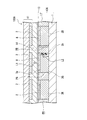
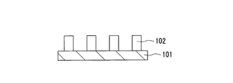
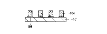
- FIG. 2 is a schematic cross-sectional view showing the manufacturing method of Example 1.
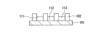
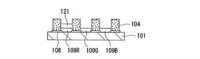
- FIG. 2 is a schematic cross-sectional view showing the manufacturing method of Example 1.
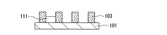
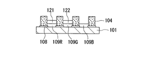
- FIG. 2 is a schematic cross-sectional view showing the manufacturing method of Example 1.
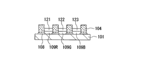
- FIG. 2 is a schematic cross-sectional view showing the manufacturing method of Example 1.
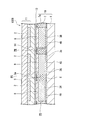
- FIG. 10 is a schematic cross-sectional view showing the production method of Example 2.
- FIG. 10 is a schematic cross-sectional view showing the production method of Example 2.
- FIG. 10 is a schematic cross-sectional view showing the production method of Example 2.
- FIG. 10 is a schematic cross-sectional view showing the production method of Example 2.
- FIG. 10 is a schematic cross-sectional view showing the production method of Example 2.
- FIG. 10 is a schematic cross-sectional view showing the production method of Example 2.
- FIG. 6 is a schematic cross-sectional view showing the production method of Example 3.
- FIG. 10 is a schematic cross-sectional view showing the production method of Example 2.
- FIG. 10 is a schematic cross-sectional view showing the production method of Example 4.
- FIG. 10 is a schematic cross-sectional view showing the production method of Example 4.
- FIG. 10 is a schematic cross-sectional view showing the production method of Example 4.
- FIG. 10 is a schematic cross-sectional view showing the production method of Example 4.
- FIG. 10 is a schematic cross-sectional view showing the production method of Example 4.
- FIG. 10 is a schematic cross-sectional view showing the production method of Example 4.
- FIG. 10 is a schematic cross-sectional view showing the production method of Example 4.
- FIG. 1 is a schematic cross-sectional view of a display device 100 according to the first embodiment.
- the display device 100 includes a phosphor substrate 10, a substrate 13, a light source 11, and an adhesive layer 14.
- the substrate 13 is provided between the phosphor substrate and the light source 11.
- the light source 11 includes the light emitting element 2. From the light emitting element 2, excitation light L1 incident on the phosphor substrate 10 is emitted.
- the adhesive layer 14 joins the light source 11 and the phosphor substrate 10.
- an adhesive layer such as a general ultraviolet curable resin or a thermosetting resin can be used.
- the adhesive layer 14 is the peripheral portion of the phosphor substrate 10 and the light source 11, and is disposed between the phosphor substrate 10 and the light source 11.
- an inert gas such as nitrogen gas or argon gas may be sealed in the region surrounded by 14.
- a hygroscopic agent such as barium oxide in the enclosed inert gas because, for example, when the excitation light source is an organic EL, the influence of moisture on the organic EL can be reduced more effectively.
- this embodiment is not limited to these members and forming methods.
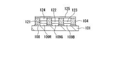
- FIG. 2 is a schematic cross-sectional view of the phosphor substrate 10 of the first embodiment.
- the substrate 1 is disposed so as to face the phosphor substrate 10.
- the phosphor substrate 10 includes one pixel, which is a minimum unit that forms an image, by three dots that respectively display red, green, and blue.
- a dot that performs red display is referred to as a red pixel PR
- a dot that performs green display is referred to as a green pixel PG
- a dot that performs blue display is referred to as a blue pixel PB.
- ultraviolet light or blue light is emitted from the outside of the substrate 13 as the excitation light L1.
- red fluorescence L2 is generated in the red pixel PR
- green fluorescence L2 is generated in the green pixel PG
- blue fluorescence L2 is generated in the blue pixel PB.
- full color display is performed by these three color lights of red, green and blue.
- the phosphor substrate 10 includes a substrate 1, phosphor layers 3R, 3G, and 3B, a partition wall 7 and a planarizing layer 8.
- the phosphor layers 3R, 3G, and 3B are provided on the substrate 1.
- the phosphor layers 3 ⁇ / b> R, 3 ⁇ / b> G, and 3 ⁇ / b> B generate fluorescence L ⁇ b> 2 by excitation light L ⁇ b> 1 incident from the outside of the substrate 13 that is disposed to face the substrate 1.
- the barrier ribs 7 surround the side surfaces of the phosphor layers 3R, 3G, 3B.
- the planarization layer 8 is provided on the surface of the phosphor layers 3R, 3G, 3B.
- the excitation light incident surface 3a on which the excitation light L1 of the phosphor layers 3R, 3G, 3B is incident is exposed from the opening of the partition wall 7. That is, the excitation light incident surface 3a is a surface on which the excitation light L1 emitted from the light emitting element 2 of the light source 11 can enter.
- the excitation light L1 is converted into fluorescence L2 in the phosphor layers 3R, 3G, 3B.
- the fluorescence L2 is emitted from the emission surface 3b of the phosphor layers 3R, 3G, 3B.
- the phosphor layers 3R, 3G and 3B are composed of a plurality of phosphor layers divided for each dot.
- the plurality of phosphor layers 3R, 3G, and 3B are made of different phosphor materials in order to emit color light of different colors depending on the dots.
- the phosphor materials constituting the plurality of phosphor layers 3R, 3G, 3B may have different refractive indexes.
- the phosphor layers 3R, 3G, 3B are made of, for example, a thin film having a rectangular shape in plan view.
- a wavelength selective transmission / reflection member that transmits the excitation light L1 and reflects the fluorescence L2 emitted from the phosphor layers 3R, 3G, and 3B is formed on the outer surface side of the excitation light incident surface 3a of the phosphor layers 3R, 3G, and 3B. May be.
- transmitting the excitation light means transmitting at least the light corresponding to the peak wavelength of the excitation light
- reflecting the fluorescence generated in the phosphor layers 3R, 3G, 3B means that the phosphor layers 3R, 3G are reflected.
- 3B is reflected at least at the light corresponding to each emission peak wavelength.
- the partition wall 7 is configured by dispersing light scattering particles 7a therein.
- the partition wall 7 is formed of a material containing a resin and light scattering particles.
- the partition 7 whole is formed with the material containing resin and light-scattering particle
- only the portions of the partition walls 7 that are in contact with the phosphor layers 3R, 3G, and 3B may be formed of a material containing a resin and light scattering particles. That is, it is only necessary that at least a portion of the partition wall 7 in contact with the phosphor layers 3R, 3G, and 3B has light scattering properties.
- the partition wall 7 may be white. Specifically, the partition wall 7 may be formed including a white resist. In addition, the whole partition 7 may be formed including a white resist, or only a portion of the partition 7 in contact with the phosphor layers 3R, 3G, and 3B may be formed including a white resist. That is, it is only necessary that at least portions of the partition walls 7 that are in contact with the phosphor layers 3R, 3G, and 3B are white. Thereby, compared with the case where a partition is black, fluorescence L2 can be made hard to be absorbed by the partition 7.
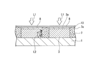
- FIG. 3A and 3B are schematic diagrams for explaining the operation of the partition wall 7 of the display device 100 according to the first embodiment.
- FIG. 3A is a schematic cross-sectional view showing the display device 100 according to the present embodiment.
- FIG. 3B is a schematic cross-sectional view showing a conventional display device 100X.
- the light scattering particles 7 a are dispersed and formed in the partition wall 7 surrounding the side surface of the phosphor layer 3.
- L2 is scattered by the light scattering particles 7a in contact with the partition walls 7, and the fluorescence L2 is not easily absorbed by the partition walls 7.
- the loss of the fluorescence L2 due to the fluorescence L2 generated in the phosphor layer 3 being absorbed by the partition walls 7 can be reduced, and the fluorescence L2 can be sufficiently extracted outside.
- the manufacture is facilitated.
- an excitation light source is provided outside the substrate.
- the excitation light source is an organic EL
- the phosphor layers, the color filter layers, the partition layers, etc. are sequentially laminated after the layers of the organic EL are laminated or the cathode of the organic EL.
- Manufacturing is very difficult because it is necessary to bond the substrate formed up to 1 to the phosphor substrate on which the barrier layer, color filter layer, and phosphor layer are formed on another substrate in an atmosphere excluding water and oxygen. .
- the excitation light source is an LED and the light transmission is adjusted by a liquid crystal element
- the liquid crystal substrate and the phosphor substrate can be manufactured separately if the substrate is provided, so that it is manufactured easily and at low cost. be able to.
- the effect of sealing and protecting the organic EL element is great.
- Organic EL elements are easily degraded by the influence of moisture and oxygen.
- the structure in which sealing is performed with the two substrates of the substrate 13 and the substrate 1 has a greater chance of moisture and oxygen intrusion into the organic EL element than the structure in which the sealing is performed only with the substrate 1.
- an organic EL element a partition that may contain residual moisture through a development process, a phosphor that may contain a residual organic solvent, a color filter, and the like Since it can isolate
- the phosphor When the distance between the light source and the phosphor is short, the phosphor is likely to deteriorate due to heat generated from the light source. On the other hand, when there is an excitation light source outside the substrate 13, a sufficient distance between the light source and the phosphor can be secured, and deterioration of the phosphor due to heat generation of the excitation light source can be suppressed.
- the structural member and the formation method of the fluorescent substance substrate 10 concerning this embodiment are explained concretely, the structural member and the formation method of the fluorescent substance substrate 10 are not limited to this.
- substrate As the substrate 1 for the phosphor substrate 10 used in the present embodiment, it is necessary to take out the fluorescence L2 from the phosphor layers 3R, 3G, 3B to the outside. Therefore, the light emitting regions of the phosphor layers 3R, 3G, 3B Therefore, it is necessary to transmit the fluorescence L2.
- the phosphor substrate 10 include an inorganic material substrate made of glass, quartz, and the like, a plastic substrate made of polyethylene terephthalate, polycarbazole, polyimide, and the like, but this embodiment is not limited to these substrates. Absent.
- the phosphor layers 3R, 3G, and 3B of the present embodiment absorb excitation light L1 from the light emitting element 2 such as an ultraviolet light emitting organic EL element, a blue light emitting organic EL element, an ultraviolet light emitting LED, and a blue LED, and red, green, It is composed of a red phosphor layer 3R that emits blue light, a green phosphor layer 3G, and a blue phosphor layer 3B.
- the blue phosphor layer 3B is not provided, and the blue excitation light L1 may be emitted from the blue pixel PB.
- the blue phosphor layer 3B is not provided, and the excitation light L1 having directivity is scattered, and isotropically emitted so that it can be extracted outside.
- a simple light scattering layer may be applied.
- a phosphor layer that emits cyan light and yellow light to the pixels as necessary.
- the color reproduction range can be further expanded as compared with a display device using pixels that emit three primary colors of red, green, and blue.
- the phosphor layers 3R, 3G, and 3B may be composed of only the phosphor materials exemplified below, and may optionally contain additives and the like, and these materials are polymer materials (binding resins). Or the structure disperse
- a known phosphor material can be used as the phosphor material of the present embodiment.
- Such phosphor materials are classified into organic phosphor materials and inorganic phosphor materials, and specific examples of these compounds are shown below, but the phosphor materials are not limited to these materials. .
- Organic phosphor materials include blue fluorescent dyes, stilbenzene dyes: 1,4-bis (2-methylstyryl) benzene, trans-4,4′-diphenylstilbenzene, coumarin dyes: 7-hydroxy- 4-methylcoumarin, ethyl 2,3,6,7-tetrahydro-11-oxo-1H, 5H, 11H- [1] benzopyrano [6,7,8-ij] quinolidine-10-carboxylate (coumarin 314), 10-acetyl-2,3,6,7-tetrahydro-1H, 5H, 11H- [1] benzopyrano [6,7,8-ij] quinolizin-11-one (coumarin 334), anthracene dye: 9,10 Bis (phenylethynyl) anthracene, perylene and the like can be mentioned.
- a green fluorescent dye a coumarin dye: 2,3,5,6-1H, 4H-tetrahydro-8-trifluoromethylquinolidine (9,9a, 1-gh) coumarin (coumarin 153), 3- ( 2'-benzothiazolyl) -7-diethylaminocoumarin (coumarin 6), 3- (2'-benzoimidazolyl) -7-N, N-diethylaminocoumarin (coumarin 7), 10- (benzothiazol-2-yl) -2 3,6,7-tetrahydro-1H, 5H, 11H- [1] benzopyrano [6,7,8-ij] quinolizin-11-one (coumarin 545), coumarin 545T, coumarin 545P, naphthalimide dye: basic yellow 51, solvent yellow 11, solvent yellow 98, solvent yellow 116, solvent yellow 43 Solvent yellow 44, perylene dye: lumogen yellow, rumogen green, solvent green 5, fluorescein dye, azo dye
- the red fluorescent dye includes cyanine dye: 4-dicyanomethylene-2-methyl-6- (p-dimethylaminostyryl) -4H-pyran, pyridine dye: 1-ethyl-2- [4- ( p-dimethylaminophenyl) -1,3-butadienyl] -pyridinium-perchlorate (pyridine 1) and xanthene dyes: rhodamine B, rhodamine 6G, rhodamine 3B, rhodamine 101, rhodamine 110, basic violet 11, sulforhodamine 101 Basic Violet 11, Basic Red 2, Perylene dyes: Lumogen Orange, Lumogen Pink, Lumogen Red, Solvent Orange 55, Oxazine Dye, Chrysene Dye, Thioflavin Dye, Pyrene Dye, Anthracene Dye, Acridone Dye, Kuridine dyes, fluorene dyes, terphenyl dyes, ethen
- each color phosphor When an organic phosphor material is used as each color phosphor, it is desirable to use a dye that is not easily degraded by blue light, ultraviolet light, or external light of the backlight. In this respect, it is particularly preferable to use a perylene dye having excellent light resistance and a high quantum yield.
- the binder resin for dispersing the organic phosphor material is preferably a translucent resin, for example, an acrylic resin, a melamine resin, a polyester resin, a polyurethane resin, an alkyd resin, an epoxy resin, a butyral resin, Polysilicone resin, polyamide resin, polyimide resin, melanin resin, phenol resin, polyvinyl alcohol, polyvinyl hydrin, hydroxyethyl cellulose, carboxyl methyl cellulose, aromatic sulfonamide resin, urea resin, benzoguanamine resin, triacetyl cellulose (TAC), polyether Sulphone, polyetherketone, nylon, polystyrene, melamine beads, polycarbonate, polyvinyl chloride, polyvinylidene chloride, polyvinyl acetate, polyethylene, polymethyl methacrylate Poly MBS, medium density polyethylene, high density polyethylene, polytetrafluoroethylene, poly trifluorochloroethylene, polytetrafluoro
- blue phosphors such as Sr 2 P 2 O 7 : Sn 4+ , Sr 4 Al 14 O 25 : Eu 2+ , BaMgAl 10 O 17 : Eu 2+ , SrGa 2 S 4 are used.
- Y 2 O 2 S Eu 3+ , YAlO 3 : Eu 3+ , Ca 2 Y 2 (SiO 4 ) 6 : Eu 3+ , LiY 9 (SiO 4 ) 6 O 2 : Eu 3+ , YVO 4 : Eu 3+ , CaS: Eu 3+ , Gd 2 O 3 : Eu 3+ , Gd 2 O 2 S: Eu 3+ , Y (P, V) O 4 : Eu 3+ , Mg 4 GeO 5.5 F: Mn 4+ , Mg 4 GeO 6 : Mn 4+ , K 5 Eu 2.5 (WO 4 ) 6.25 , Na 5 Eu 2.5 (WO 4 ) 6.25 , K 5 Eu 2.5 (MoO 4 ) 6.25 , Na 5 Eu 2.5 (MoO 4 ) 6.25 and the like.
- the inorganic phosphor may be subjected to a surface modification treatment as necessary.
- a surface modification treatment physical treatment by chemical treatment such as a silane coupling agent or addition of fine particles of submicron order, etc. And the like due to the combined treatment thereof.
- an inorganic material it is preferable to use an inorganic material.
- the average particle size (d 50 ) is preferably 0.5 ⁇ m to 50 ⁇ m. When the average particle size is 1 ⁇ m or less, the luminous efficiency of the phosphor is drastically reduced. Moreover, when it is 50 ⁇ m or more, it becomes difficult to pattern at a high resolution.
- the phosphor layer is formed by using a phosphor layer forming coating solution obtained by dissolving and dispersing the phosphor material and the resin material in a solvent, using a spin coating method, a dipping method, a doctor blade method, a discharge coating method, a spraying method.
- Known wet processes such as coating methods such as coating methods, ink jet methods, letterpress printing methods, intaglio printing methods, screen printing methods, printing methods such as micro gravure coating methods, etc.
- It can be formed by a known dry process such as a vapor deposition method, molecular beam epitaxy (MBE) method, sputtering method, organic vapor deposition (OVPD) method, or a laser transfer method.
- the film thickness of the phosphor is usually about 100 nm to 100 ⁇ m, preferably 1 ⁇ m to 100 ⁇ m. If the film thickness is less than 100 nm, it is impossible to sufficiently absorb the light emitted from the light source. Therefore, the light emission efficiency is lowered, and the color purity is deteriorated by mixing the transmitted light of the excitation light with the required color. Arise. Further, in order to increase the absorption of light emitted from the light source and reduce the transmitted light of the excitation light to such an extent that the color purity is not adversely affected, the film thickness is preferably 1 ⁇ m or more. Further, if the film thickness exceeds 100 ⁇ m, the light emitted from the light source is already sufficiently absorbed. Therefore, the efficiency is not increased but only the material is consumed, and the material cost is increased.
- the light scattering particles may be made of an organic material or an inorganic material, but may be made of an inorganic material. It is preferable. This makes it possible to diffuse or scatter light having directivity from the outside (for example, a light emitting element) more isotropically and effectively. Further, by using an inorganic material, it is possible to provide a light scattering layer that is stable to light and heat. Moreover, it is preferable that the light scattering particles have high transparency.
- the light scattering particles are preferably particles in which fine particles having a higher refractive index than the base material are dispersed in a low refractive index base material.
- the particle size of the light scattering particle is in the Mie scattering region, so the particle size of the light scattering particle is 100 nm to 500 nm. The degree is preferred.
- the main component is an oxide of at least one metal selected from the group consisting of silicon, titanium, zirconium, aluminum, indium, zinc, tin, and antimony. Examples thereof include particles (fine particles).
- particles (inorganic fine particles) made of an inorganic material for example, silica beads (refractive index: 1.44), alumina beads (refractive index: 1.63), titanium oxide. Beads (refractive index anatase type: 2.50, rutile type: 2.70), zirconia bead (refractive index: 2.05), zinc oxide beads (refractive index: 2.00), barium titanate (BaTiO 3 ) (Refractive index: 2.4).
- particles (organic fine particles) made of an organic material are used as the light scattering particles, for example, polymethyl methacrylate beads (refractive index: 1.49), acrylic beads (refractive index: 1.50), acrylic- Styrene copolymer beads (refractive index: 1.54), melamine beads (refractive index: 1.57), high refractive index melamine beads (refractive index: 1.65), polycarbonate beads (refractive index: 1.57), Styrene beads (refractive index: 1.60), crosslinked polystyrene beads (refractive index: 1.61), polyvinyl chloride beads (refractive index: 1.60), benzoguanamine-melamine formaldehyde beads (refractive index: 1.68), Examples thereof include silicone beads (refractive index: 1.50).
- the resin material used by mixing with the above-described light scattering particles is preferably a translucent resin.
- the resin material include acrylic resin (refractive index: 1.49), melamine resin (refractive index: 1.57), nylon (refractive index: 1.53), polystyrene (refractive index: 1.60).
- Melamine beads (refractive index: 1.57), polycarbonate (refractive index: 1.57), polyvinyl chloride (refractive index: 1.60), polyvinylidene chloride (refractive index: 1.61), polyvinyl acetate ( Refractive index: 1.46), polyethylene (refractive index: 1.53), polymethyl methacrylate (refractive index: 1.49), poly MBS (refractive index: 1.54), medium density polyethylene (refractive index: 1) .53), high density polyethylene (refractive index: 1.54), tetrafluoroethylene (refractive index: 1.35), poly (trifluoroethylene chloride) (refractive index: 1.42), polytetrafluoroethylene (refractive index) : .35), and the like.
- Partition wall 7 of this embodiment is formed of a material containing resin and light scattering particles 7a. Like the light scattering layer described above, it is preferable to disperse light scattering fine particles having a higher refractive index than that of the resin in a low refractive index resin. In addition, in order for blue light to be effectively scattered by the light-scattering partition wall, the particle size of the light-scattering particles needs to be in the Mie scattering region. About 500 nm is preferable. As the resin, for example, the resin materials listed in [0058] can be used.
- the light scattering particles 7a for example, light scattering particles such as those listed in [0054], [0055], [0056], and [0057] can be used.
- an alkali-soluble resin as a constituent resin of the partition wall material and adding a photopolymerizable monomer, a photopolymerization initiator, and a solvent, the partition wall material can be made into a photoresist and can be patterned by photolithography. .
- the vertical and horizontal sizes of the openings (one section of the phosphor layer) of the partition walls 7 are preferably about 20 ⁇ m ⁇ 20 ⁇ m to about 500 ⁇ m ⁇ 500 ⁇ m.
- the partition wall 7 preferably has a reflectance of 80% or more in the CIE 1976 L * a * b display system.
- a thin black barrier rib layer may be inserted on the light extraction direction side of the light scattering barrier compared with a light scattering barrier of about 0.01 ⁇ m to 3 ⁇ m. Furthermore, in order to prevent excitation light designed to enter a certain pixel from leaking to adjacent pixels and causing color mixing, the light of the light-scattering partition wall is absorbed for the purpose of absorbing the light entering the adjacent pixels.
- a thin black barrier rib layer may be inserted on the side opposite to the take-out direction as compared with a light-scattering barrier rib of about 0.01 ⁇ m to 3 ⁇ m.
- Providing liquid repellency to partition walls When the phosphor layer is patterned by a dispenser method, an ink jet method, or the like, it is essential to impart liquid repellency to the partition wall in order to prevent the phosphor solution from overflowing from the partition wall and mixing colors between adjacent pixels.
- a method for imparting liquid repellency to the partition include the following methods.
- (1) Fluorine plasma treatment For example, as disclosed in Japanese Patent Application Laid-Open No. 2000-76979, a plasma treatment is performed on a substrate on which a partition wall is formed under a condition in which an introduced gas is a fluorine-based gas. Liquidity can be imparted.
- a liquid repellency can be imparted to the partition walls by adding a fluorinated surface modifier to the light scattering partition material.
- a fluorinated surface modifier for example, a UV curable surface modifier Defenser (manufactured by DIC Corporation), Mega Fuck, or the like can be used.
- Partition shape The shape of the partition wall is preferably a tapered shape in which the opening of the partition wall is wider on the incident side than on the output substrate side so that the backlight light does not enter the adjacent pixel of the pixel that should be incident.
- the ratio of the partition wall height to the lateral width of the partition wall is 1 or less.
- Color filter In the phosphor substrate 10 of the present embodiment, it is preferable to provide a color filter between the substrate 1 on the light extraction side and the phosphor layers 3R, 3G, 3B.
- a conventional color filter can be used as the color filter.
- the color filter by providing the color filter, the color purity of the red pixel PR, the green pixel PG, and the blue pixel PB can be increased, and the color reproduction range of the display device 100 can be expanded.
- the blue color filter facing the blue phosphor layer 3B, the green color filter facing the green phosphor layer 3G, and the red color filter facing the red phosphor layer 3R are phosphor layers 3R, 3G, Since the excitation light that excites 3B is absorbed, it is possible to reduce or prevent light emission of the phosphor layers 3R, 3G, and 3B due to external light, and it is possible to reduce or prevent a decrease in contrast. Further, the blue color filter, the green color filter, and the red color filter can prevent the excitation light L1 that is not absorbed and transmitted through the phosphor layers 3R, 3G, and 3B from leaking to the outside. , 3G, 3B and the color purity of the light emission due to the mixed color of the excitation light L1 can be prevented.
- the phosphor substrate 10 of the present embodiment may be provided with a light source that emits excitation light that irradiates the phosphor layers 3R, 3G, and 3B outside the substrate 13 to constitute a display device.
- a light source for exciting the phosphor layers 3R, 3G, 3B ultraviolet light and blue light are preferable.
- the light source that emits the excitation light include an ultraviolet LED, a blue LED, an ultraviolet light emitting inorganic EL, a blue light emitting inorganic EL, an ultraviolet light emitting organic EL, and a blue light emitting organic EL. It is not limited.
- the light source known ultraviolet LED, blue LED, ultraviolet light emitting inorganic EL, blue light emitting inorganic EL, ultraviolet light emitting organic EL, blue light emitting organic EL and the like can be used, and are not particularly limited. It can be produced by a known production method.
- the ultraviolet light preferably emits light having a main light emission peak of 360 nm to 410 nm, and the blue light preferably has light emission of a main light emission peak of 410 nm to 480 nm. It is desirable that the light source has directivity. Directivity refers to the property that the intensity of light varies depending on the direction. The directivity may be provided at the time when light enters the phosphor layer.
- the light source desirably makes parallel light incident on the phosphor layer.
- the degree of directivity of the light source is 30 degrees or less, more preferably 10 degrees or less. This is because when the half-value width is larger than 30 degrees, light emitted from the backlight is incident on a pixel other than a desired pixel and excites an undesired phosphor to reduce color purity and contrast.
- an LED light emitting diode
- a known LED can be used as the LED.
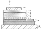
- an ultraviolet light emitting inorganic LED and a blue light emitting inorganic LED are suitable. These LEDs include, for example, a first buffer layer 23, an n-type contact layer 24, a second n-type cladding layer 25, a first n-type cladding layer 26, an active layer 27, a first layer on one surface of the substrate 9.
- a p-type cladding layer 28, a second p-type cladding layer 29, and a second buffer layer 30 are sequentially stacked, a cathode 22 is formed on the n-type contact layer 24, and an anode 21 is formed on the second buffer layer 30.
- the specific structure of LED is not restricted to the above-mentioned thing.
- the active layer 27 is a layer that emits light by recombination of electrons and holes.
- the active layer material of the active layer 27 a known active layer material for LED can be used.
- an active layer material for example, as an ultraviolet active layer material, AlGaN, InAlN, In a Al b Ga 1-ab N (0 ⁇ a, 0 ⁇ b, a + b ⁇ 1), blue active layer material In z Ga 1 -z N (0 ⁇ z ⁇ 1) and the like are exemplified, but the active layer material is not limited thereto.
- the active layer 27 a single quantum well structure or a multiple quantum well structure can be used.
- the active layer of the quantum well structure may be either n-type or p-type.
- the half-value width of the emission wavelength is narrowed by band-to-band emission, and emission with good color purity is obtained. Therefore, it is preferable.
- the active layer 27 may be doped with at least one of a donor impurity and an acceptor impurity. If the crystallinity of the active layer doped with impurities is the same as that of non-doped, doping with donor impurities can further increase the emission intensity between bands as compared with non-doped ones.
- the acceptor impurity is doped, the peak wavelength can be shifted to a lower energy side by about 0.5 eV than the peak wavelength of interband light emission, but the full width at half maximum is increased.
- both the acceptor impurity and the donor impurity are doped, the light emission intensity can be further increased as compared with the light emission intensity of the active layer doped only with the acceptor impurity.
- the conductivity type of the active layer is preferably doped with a donor impurity such as Si to be n-type.
- the n-type cladding layers 25 and 26 known n-type cladding layer materials for LEDs can be used.
- the n-type cladding layer is composed of two layers of the first n-type cladding layer 26 and the second n-type cladding layer 25, but the n-type cladding layer may be a single layer, Three or more layers may be used.
- the n-type cladding layer By forming the n-type cladding layer with a material formed of an n-type semiconductor having a band gap energy larger than that of the active layer 27, a potential barrier against holes is formed between the n-type cladding layer and the active layer 27. Can be confined in the active layer.
- the n-type cladding layers 25 and 26 can be formed of n-type Inx Ga 1- x N (0 ⁇ x ⁇ 1), but the n-type cladding layers 25 and 26 are limited to these. is not.
- the p-type cladding layers 28 and 29 a known p-type cladding layer material for LED can be used.
- the p-type cladding layer is composed of two layers of the first p-type cladding layer 28 and the second p-type cladding layer 29, but the p-type cladding layer may be a single layer, Three or more layers may be used.
- the p-type cladding layer By configuring the p-type cladding layer with a material formed of a p-type semiconductor having a larger band gap energy than the active layer 27, a potential barrier against electrons is formed between the p-type cladding layer and the active layer 27, and the electrons are active. It becomes possible to confine in the layer 27.
- the p-type cladding layers 28 and 29 can be formed of Aly Ga1-y N (0 ⁇ y ⁇ 1), but the p-type cladding layers 28 and 29 are not limited to these.
- n-type contact layer 24 a known contact layer material for LED can be used.
- an n-type contact layer made of n-type GaN can be formed as a layer for forming an electrode (cathode 22) in contact with the n-type cladding layer.
- a p-type contact layer made of p-type GaN as a layer for forming the electrode (anode 21) in contact with the p-type cladding layer.
- this contact layer need not be formed if the second n-type cladding layer 25 and the second p-type cladding layer 29 are made of GaN.
- the second n-type and p-type cladding layers are not necessary. Can be used as a contact layer.
- a known film formation process for LED can be used, but the film formation process is not particularly limited thereto.
- a vapor phase growth method such as MOVPE (metal organic vapor phase epitaxy), MBE (molecular beam vapor phase epitaxy), HDVPE (hydride vapor phase epitaxy), for example, sapphire (C plane, A plane, R ), SiC (including 6H—SiC, 4H—SiC), spinel (MgAl 2 O 4 , especially its (111) plane), ZnO, Si, GaAs, or other oxide single crystal substrates (such as NGO)
- MOVPE metal organic vapor phase epitaxy
- MBE molecular beam vapor phase epitaxy
- HDVPE hydrogen vapor phase epitaxy
- sapphire C plane, A plane, R
- SiC including 6H—SiC, 4H—SiC
- spinel MgAl 2 O 4 , especially its (111) plane
- an organic EL element can be used as the light emitting element 2B.
- a known organic EL can be used.
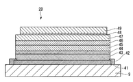
- the organic EL element 2B includes, for example, an anode 41, a hole injection layer 43, a hole transport layer 44, a light emitting layer 45, a hole prevention layer 46, an electron transport layer 47, an electron injection layer 48, and a cathode 49 on one surface of the substrate 9.
- An edge cover 42 is formed so as to cover the end face of the anode 41.
- the organic EL element 2B only needs to include an organic EL layer including at least a light emitting layer (organic light emitting layer) 45 made of an organic light emitting material between the anode 41 and the cathode 49.
- a light emitting layer organic light emitting layer
- the specific configuration is as described above. It is not limited to.
- the layers from the hole injection layer 43 to the electron injection layer 48 may be referred to as an organic EL layer.
- the organic EL element 2B is provided in a matrix corresponding to each of the red pixel PR, the green pixel PG, and the blue pixel PB shown in FIG. 1, and is individually controlled to be turned on / off.
- the driving method of the plurality of organic EL elements 2B may be active matrix driving or passive matrix driving. A configuration example using an active matrix organic EL element will be described in detail later.
- substrate As the substrate 9 used in this embodiment, for example, an inorganic substrate made of glass, quartz, etc., a plastic substrate made of polyethylene terephthalate, polycarbazole, polyimide, etc., an insulating substrate such as a ceramic substrate made of alumina, or the like, or A metal substrate made of aluminum (Al), iron (Fe), or the like, or a substrate in which an insulating material made of silicon oxide (SiO 2 ) or an organic insulating material is coated on the substrate, or a metal substrate made of Al or the like Examples thereof include a substrate whose surface is subjected to insulation treatment by a method such as anodization.
- a substrate in which the plastic substrate is coated with an inorganic material, and a substrate in which the metal substrate is coated with an inorganic insulating material are more preferable. This makes it possible to eliminate moisture permeation that may occur when a plastic substrate is used as an organic EL substrate.
- leakage (short) due to protrusions on the metal substrate which is the biggest problem when a metal substrate is used as an organic EL substrate (the film thickness of the organic EL is very thin, about 100 nm to 200 nm. It is known that leakage (short-circuit) occurs in the current at (1).
- a substrate that does not melt at a temperature of 500 ° C. or lower and does not cause distortion.
- a general metal substrate has a coefficient of thermal expansion different from that of glass, it is difficult to form a TFT on the metal substrate with a conventional production apparatus, but the linear expansion coefficient is 1 ⁇ 10 ⁇ 5 / ° C. or less.
- a metal substrate which is an iron-nickel alloy of this type and adjusting the linear expansion coefficient to glass, it becomes possible to form TFTs on the metal substrate at low cost using a conventional production apparatus.
- the heat-resistant temperature is very low, it is possible to transfer and form the TFT on the plastic substrate by forming the TFT on the glass substrate and then transferring the TFT to the plastic substrate. is there.
- the substrate used is from the organic EL layer. In order to extract emitted light to the outside, it is necessary to use a transparent or translucent substrate.
- the anode 41 and the cathode 49 used in the present embodiment function as a first electrode and a second electrode that supply current to the organic EL layer.
- the anode 41 that is the first electrode is disposed on the substrate 9 side with the organic EL layer interposed therebetween, and the cathode 49 that is the second electrode is disposed on the side opposite to the substrate 9 with the organic EL layer interposed therebetween.
- this relationship may be reversed.
- the anode 41 that is the first electrode may be disposed on the side opposite to the substrate 9 with the organic EL layer interposed therebetween, and the cathode 49 that is the second electrode may be disposed on the substrate 9 side with the organic EL layer interposed therebetween.
- Specific compounds and formation methods are exemplified below, but the compounds and formation methods are not limited to these.
- an electrode material for forming the anode 41 and the cathode 49 a known electrode material can be used.
- an electrode material for forming the anode gold (Au), platinum (Pt), nickel (Ni) or the like having a work function of 4.5 eV or more is used from the viewpoint of efficiently injecting holes into the organic EL layer.
- Metals and oxides (ITO) made of indium (In) and tin (Sn), oxides of tin (Sn) (SnO 2 ), oxides of indium (In) and zinc (Zn) (IZO), etc. It is mentioned as a transparent electrode material.
- metals such as barium (Ba) and aluminum (Al), or alloys such as Mg: Ag alloy and Li: Al alloy containing these metals.
- the anode 41 and the cathode 49 can be formed by a known method such as an EB vapor deposition method, a sputtering method, an ion plating method, or a resistance heating vapor deposition method using the above materials. It is not limited to the forming method. If necessary, the formed electrode can be patterned by a photolithographic fee method or a laser peeling method, or a patterned electrode can be directly formed by combining with a shadow mask.
- the film thickness is preferably 50 nm or more. When the film thickness is less than 50 nm, the wiring resistance is increased, which may increase the drive voltage.
- a translucent electrode is used as the anode 41. It is preferable to use it.
- the material used here it is possible to use a metal translucent electrode alone or a combination of a metal translucent electrode and a transparent electrode material, but as a translucent electrode material, from the viewpoint of reflectance and transmittance Silver is preferred.
- the film thickness of the semitransparent electrode is preferably 5 nm to 30 nm. When the film thickness is less than 5 nm, light cannot be sufficiently reflected, and interference effects cannot be obtained sufficiently.
- the film thickness exceeds 30 nm, the light transmittance is drastically reduced, so that the luminance and efficiency may be lowered.
- an electrode with high reflectivity that reflects light as the cathode 49.
- electrode materials used in this case include reflective metal electrodes such as aluminum, silver, gold, aluminum-lithium alloys, aluminum-neodymium alloys, and aluminum-silicon alloys, transparent electrodes, and reflective metal electrodes (reflective electrodes). The electrode etc. which combined these are mentioned.
- the anode 41 When light emitted from the organic EL layer is taken out from the cathode 49 side, the anode 41 may be formed of a highly reflective electrode and the cathode 49 may be a translucent electrode, contrary to the above.
- Organic EL layer used in the present embodiment may be a single layer structure of an organic light emitting layer or a multilayer structure of an organic light emitting layer and a charge transport layer. Specifically, the following configurations may be mentioned. The configuration is not limited by these. In the example of FIG. 5, the following configuration (8) is used. In the following description, holes and electrons are referred to as charges, and a layer that injects charges from the anode 41 or the cathode 49 toward the light emitting layer 45 (hole injection layer or electron injection layer) is referred to as a charge injection layer.
- a layer (hole transport layer, electron transport layer) that transports charges injected from the anode 41 or the cathode 49 by the charge injection layer toward the light emitting layer 45 is referred to as a charge transport layer, and the charge injection layer and the charge transport layer are collectively referred to. Therefore, it may be referred to as a charge injection / transport layer.
- Organic light emitting layer (2) Hole transport layer / organic light emitting layer (3) Organic light emitting layer / electron transport layer (4) Hole transport layer / organic light emitting layer / electron transport layer (5) Hole injection layer / Hole transport layer / organic light emitting layer / electron transport layer (6) hole injection layer / hole transport layer / organic light emitting layer / electron transport layer / electron injection layer (7) hole injection layer / hole transport layer / organic Light emitting layer / Hole prevention layer / Electron transport layer (8) Hole injection layer / Hole transport layer / Organic light emitting layer / Hole prevention layer / Electron transport layer / Electron injection layer (9) Hole injection layer / Hole Transport layer / electron prevention layer / organic light emitting layer / hole prevention layer / electron transport layer / electron injection layer
- Each layer of the organic light emitting layer, hole injection layer, hole transport layer, hole prevention layer, electron prevention layer, electron transport layer and electron injection layer may have a single layer structure or a multilayer structure.
- the organic light emitting layer 45 may be composed of only an organic light emitting material exemplified below, or may be composed of a combination of a light emitting dopant and a host material, and optionally a hole transport material, an electron transport material, Additives (donor, acceptor, etc.) may be included, and these materials may be dispersed in a polymer material (binding resin) or an inorganic material. From the viewpoint of luminous efficiency and lifetime, a material in which a luminescent dopant is dispersed in a host material is preferable.
- organic light emitting material a known light emitting material for organic EL can be used. Such light-emitting materials are classified into low-molecular light-emitting materials, polymer light-emitting materials, and the like. Specific examples of these compounds are given below, but organic light-emitting materials are not limited to these materials.
- the light-emitting material may be classified into a fluorescent material, a phosphorescent material, and the like, and it is preferable to use a phosphorescent material with high light emission efficiency from the viewpoint of reducing power consumption.
- organic light emitting material is not limited to these materials.
- a known dopant material for organic EL can be used as the light-emitting dopant optionally contained in the light-emitting layer.
- a dopant material for example, as an ultraviolet light emitting material, p-quaterphenyl, 3,5,3,5 tetra-t-butylsecphenyl, 3,5,3,5 tetra-t-butyl-p -Fluorescent materials such as quinckphenyl.
- a fluorescent light emitting material such as a styryl derivative, bis [(4,6-difluorophenyl) -pyridinato-N, C2 ′] picolinate, iridium (III) (FIrpic), bis (4 ′, 6′-difluorophenyl) And phosphorescent organometallic complexes such as polydinato) tetrakis (1-pyrazoyl) borate, iridium (III) (FIr6), and the like.
- a fluorescent light emitting material such as a styryl derivative, bis [(4,6-difluorophenyl) -pyridinato-N, C2 ′] picolinate, iridium (III) (FIrpic), bis (4 ′, 6′-difluorophenyl) And phosphorescent organometallic complexes such as polydinato) tetrakis (1-pyrazoyl) borate, iridium
- a known host material for organic EL can be used as a host material when using a dopant.
- host materials include the low-molecular light-emitting materials, the polymer light-emitting materials, 4,4′-bis (carbazole) biphenyl, 9,9-di (4-dicarbazole-benzyl) fluorene (CPF), 3 , 6-bis (triphenylsilyl) carbazole (mCP), carbazole derivatives such as (PCF), aniline derivatives such as 4- (diphenylphosphoyl) -N, N-diphenylaniline (HM-A1), 1,3- And fluorene derivatives such as bis (9-phenyl-9H-fluoren-9-yl) benzene (mDPFB) and 1,4-bis (9-phenyl-9H-fluoren-9-yl) benzene (pDPFB).
- the charge injection / transport layer is used to more efficiently inject charges (holes, electrons) from the electrode and transport (injection) to the light emitting layer, and the charge injection layer (hole injection layer, electron injection layer). It is classified as a transport layer (hole transport layer, electron transport layer).
- the charge injecting and transporting layer may be composed only of the charge injecting and transporting material exemplified below, and may optionally contain additives (donor, acceptor, etc.), and these materials are polymer materials (conjugation). Wear resin) or a structure dispersed in an inorganic material.
- charge injection / transport material known charge transport materials for organic EL and organic photoconductors can be used. Such charge injecting and transporting materials are classified into hole injecting and transporting materials and electron injecting and transporting materials. Specific examples of these compounds are given below, but the charge injecting and transporting materials are not limited to these materials. Absent.
- hole injection hole transport materials include oxides such as vanadium oxide (V 2 O 5 ) and molybdenum oxide (MoO 3 ), inorganic p-type semiconductor materials, porphyrin compounds, N, N′-bis (3- Aromatic tertiary compounds such as methylphenyl) -N, N′-bis (phenyl) -benzidine (TPD), N, N′-di (naphthalen-1-yl) -N, N′-diphenyl-benzidine (NPD)
- TPD N, N′-di (naphthalen-1-yl) -N, N′-diphenyl-benzidine
- Low molecular weight materials such as quaternary amine compounds, hydrazone compounds, quinacridone compounds, styrylamine compounds, polyaniline (PANI), polyaniline-camphor sulfonic acid (PANI-CSA), 3,4-polyethylenedioxythiophene / polystyrene sulf
- the highest occupied molecular orbital than the hole injection transport material used for the hole transport layer 44 is used as a material used as the hole injection layer 43 in terms of more efficiently injecting and transporting holes from the anode 41.
- a material having a low energy level of (HOMO) is preferably used, and a material having a higher hole mobility than the hole injection transport material used for the hole injection layer 43 is used as the hole transport layer 44. preferable.
- acceptor a known acceptor material for organic EL can be used. Although these specific compounds are illustrated below, acceptor material is not limited to these materials.
- Acceptor materials include Au, Pt, W, Ir, POCl 3 , AsF 6 , Cl, Br, I, vanadium oxide (V 2 O 5 ), molybdenum oxide (MoO 3 ) and other inorganic materials, TCNQ (7, 7 , 8,8, -tetracyanoquinodimethane), TCNQF 4 (tetrafluorotetracyanoquinodimethane), TCNE (tetracyanoethylene), HCNB (hexacyanobutadiene), DDQ (dicyclodicyanobenzoquinone), etc.
- TNF trinitrofluorenone
- DNF dinitrofluorenone
- organic materials such as fluoranyl, chloranil and bromanyl.
- compounds having a cyano group such as TCNQ, TCNQF 4 , TCNE, HCNB, DDQ and the like are more preferable because they can increase the carrier concentration more effectively.
- Examples of electron injection electron transport materials include inorganic materials that are n-type semiconductors, oxadiazole derivatives, triazole derivatives, thiopyrazine dioxide derivatives, benzoquinone derivatives, naphthoquinone derivatives, anthraquinone derivatives, diphenoquinone derivatives, fluorenone derivatives, benzodifuran derivatives, etc. And low molecular weight materials; polymer materials such as poly (oxadiazole) (Poly-OXZ) and polystyrene derivatives (PSS).
- examples of the electron injection material include fluorides such as lithium fluoride (LiF) and barium fluoride (BaF 2 ), and oxides such as lithium oxide (Li 2 O).
- the material used as the electron injection layer 48 is more efficient in injecting and transporting electrons from the cathode 49 than the electron injection and transport material used for the electron transport layer 47. It is preferable to use a material having a high electron mobility, and it is preferable to use a material having a higher electron mobility than the electron injection transport material used for the electron injection layer 48 as the material used for the electron transport layer 47.
- the electron injection / transport material In order to further improve the electron injection and transport properties, it is preferable to dope the electron injection / transport material with a donor.
- a donor a known donor material for organic EL can be used. Although these specific compounds are illustrated below, donor material is not limited to these materials.
- Donor materials include inorganic materials such as alkali metals, alkaline earth metals, rare earth elements, Al, Ag, Cu, In, anilines, phenylenediamines, benzidines (N, N, N ′, N′-tetraphenyl) Benzidine, N, N'-bis- (3-methylphenyl) -N, N'-bis- (phenyl) -benzidine, N, N'-di (naphthalen-1-yl) -N, N'-diphenyl- Benzidine, etc.), triphenylamines (triphenylamine, 4,4′4 ′′ -tris (N, N-diphenyl-amino) -triphenylamine, 4,4′4 ′′ -tris (N-3- Methylphenyl-N-phenyl-amino) -triphenylamine, 4,4′4 ′′ -tris (N- (1-naphthyl) -N
- organic materials such as condensed polycyclic compounds (wherein the condensed polycyclic compounds may have a substituent), TTFs (tetrathiafulvalene), dibenzofuran, phenothiazine, and carbazole.
- a compound having an aromatic tertiary amine as a skeleton, a condensed polycyclic compound, and an alkali metal are more preferable because the carrier concentration can be increased more effectively.
- the organic EL layers such as the light-emitting layer 45, the hole transport layer 44, the electron transport layer 47, the hole injection layer 43, and the electron injection layer 48 are organic EL layer forming coating solutions in which the above materials are dissolved and dispersed in a solvent.
- a known wet process such as a resistance heating vapor deposition method, an electron beam (EB) vapor deposition method, a molecular beam epitaxy (MBE) method, a sputtering method, an organic vapor deposition (OVPD) method or the like, Alternatively, it can be formed by a laser transfer method or the like.
- the coating liquid for organic EL layer formation may contain the additive for adjusting the physical properties of coating liquid, such as a leveling agent and a viscosity modifier.
- the film thickness of each organic EL layer is usually about 1 nm to 1000 nm, but preferably 10 nm to 200 nm. If the film thickness is less than 10 nm, the properties (charge injection characteristics, transport characteristics, confinement characteristics) that are originally required cannot be obtained. In addition, pixel defects due to foreign matters such as dust may occur. On the other hand, if the film thickness exceeds 200 nm, the drive voltage increases due to the resistance component of the organic EL layer, leading to an increase in power consumption.
- an edge cover 42 is provided for the purpose of preventing leakage between the anode 41 and the cathode 49 at the edge portion of the anode 41 formed on the substrate 9 side.
- the edge cover 42 can be formed by a known method such as an EB vapor deposition method, a sputtering method, an ion plating method, or a resistance heating vapor deposition method using an insulating material, and a known dry or wet photolithography.
- the method of forming the edge cover 42 is not limited to these methods.
- a known material can be used as the material constituting the edge cover 42 and is not particularly limited in the present embodiment.
- the film thickness is preferably 100 nm to 2000 nm.
- the thickness is 100 nm or less, the insulating property is not sufficient, and leakage occurs between the anode 41 and the cathode 49, resulting in an increase in power consumption and non-light emission.
- the thickness is 2000 nm or more, the film forming process takes time, and the productivity is deteriorated and the electrode is disconnected at the edge cover 42.
- the organic EL element 2B preferably has a microcavity structure (optical microresonator structure) due to an interference effect between a reflective electrode and a translucent electrode used as the anode 41 and the cathode 49, or a dielectric multilayer film.
- a microcavity structure optical microresonator structure
- the emission spectrum can be adjusted due to the interference effect, and the emission spectrum can be adjusted by adjusting to a desired emission peak wavelength and half width. Thereby, it is possible to control the phosphor layers 3R, 3G, and 3B to a spectrum that can be excited more effectively.
- Organic EL element 2B is electrically connected to an external drive circuit.
- the organic EL element 2B may be directly connected to and driven by an external drive circuit, or a switching circuit such as a TFT is arranged in the pixel, and the external drive circuit (scan line electrode) is connected to a wiring to which the TFT or the like is connected.
- Circuit source driver
- data signal electrode circuit gate driver
- power supply circuit may be electrically connected.
- FIG. 6 is a sectional view of an organic EL element substrate 70 (light source) using the active matrix driving type organic EL element 2B.
- the organic EL element substrate 70 of the present embodiment has a TFT (driving element) 51 formed on one surface of the substrate 9. That is, the gate electrode 52 and the gate line 53 are formed, and the gate insulating film 54 is formed on the substrate body 9 so as to cover the gate electrode 52 and the gate line 53.
- An active layer (not shown) is formed on the gate insulating film 54, and a source electrode 55, a drain electrode 56 and a data line 57 are formed on the active layer, and covers the source electrode 55, the drain electrode 56 and the data line 57.
- a planarizing film 58 is formed.
- planarization film 58 does not have to have a single layer structure, and may be configured by combining another interlayer insulating film and the planarization film. Further, a contact hole 59 that reaches the drain electrode 56 through the planarizing film or the interlayer insulating film is formed, and the organic EL element that is electrically connected to the drain electrode 56 through the contact hole 59 on the planarizing film 58. A 2B anode 41 is formed. The configuration of the organic EL element 2B itself is the same as that described above.
- the TFT 51 is formed on the substrate 9 before forming the organic EL element 2B, and functions as an organic EL element driving element.
- Examples of the TFT 51 used in this embodiment include known TFTs, which can be formed using known materials, structures, and formation methods.
- a metal-insulator-metal (MIM) diode can be used instead of the TFT 51.
- Examples of the material of the active layer of the TFT 51 include inorganic semiconductor materials such as amorphous silicon (amorphous silicon), polycrystalline silicon (polysilicon), microcrystalline silicon, and cadmium selenide, zinc oxide, indium oxide-gallium oxide, and the like. Examples thereof include oxide semiconductor materials such as zinc oxide, or organic semiconductor materials such as polythiophene derivatives, thiophene oligomers, poly (p-ferylene vinylene) derivatives, naphthacene, and pentacene. Moreover, as a structure of TFT51, a stagger type
- a method for forming the active layer constituting the TFT 51 (1) a method of ion doping impurities into amorphous silicon formed by plasma induced chemical vapor deposition (PECVD), and (2) a silane (SiH 4 ) gas is used.
- PECVD plasma induced chemical vapor deposition
- SiH 4 silane
- amorphous silicon by low pressure chemical vapor deposition (LPCVD), crystallizing amorphous silicon by solid phase epitaxy to obtain polysilicon, and then ion doping by ion implantation, (3) Si 2 H A method in which amorphous silicon is formed by LPCVD using 6 gases or PECVD using SiH 4 gas, annealed by a laser such as an excimer laser, and amorphous silicon is crystallized to obtain polysilicon, followed by ion doping (Low temperature process), (4) LPCVD How is a polysilicon layer is formed by a PECVD method, a gate insulating film formed by thermal oxidation at 1000 ° C.
- LPCVD low pressure chemical vapor deposition
- the gate insulating film 54 of the TFT 51 used in this embodiment can be formed using a known material. Examples thereof include SiO 2 formed by PECVD, LPCVD, etc., or SiO 2 obtained by thermally oxidizing a polysilicon film. Further, the data line 57, the gate line 53, the source electrode 55, and the drain electrode 56 of the TFT 51 used in this embodiment can be formed using a known conductive material, for example, tantalum (Ta), aluminum (Al ), Copper (Cu), and the like.
- the TFT 51 according to this embodiment can be configured as described above, but is not limited to these materials, structures, and formation methods.
- the interlayer insulating film used in the present embodiment can be formed using a known material.
- the formation method include dry processes such as chemical vapor deposition (CVD) and vacuum deposition, and wet processes such as spin coating. Moreover, it can also pattern by the photolithographic method etc. as needed.
- the present embodiment is not limited to these materials and forming methods.
- unevenness is formed on the surface of the TFT 51 formed on the substrate 9, various wirings, and electrodes. Due to the unevenness, in the organic EL element 2B, for example, defects or disconnection of the anode 41 or the cathode 49, organic There is a possibility that the EL layer may be lost, the anode 41 and the cathode 49 may be short-circuited, or the withstand voltage may be reduced. Therefore, it is desirable to provide the planarization film 58 on the interlayer insulating film for the purpose of preventing these phenomena.
- the planarization film 58 used in the present embodiment can be formed using a known material, for example, an inorganic material such as silicon oxide, silicon nitride, or tantalum oxide, or an organic material such as polyimide, acrylic resin, or resist material. Etc.
- Examples of the method for forming the planarizing film 58 include a dry process such as a CVD method and a vacuum deposition method, and a wet process such as a spin coat method.
- the present embodiment is not limited to these materials and the formation method. .
- the planarizing film 58 may have a single layer structure or a multilayer structure.
- FIG. 7 is a schematic configuration diagram of a display device 200 including the organic EL element substrate 70.
- the display device 200 includes an organic EL element substrate 70, a phosphor substrate 10, a pixel unit 71, a gate signal driving circuit 72, a data signal driving circuit 73, a signal wiring 74, a current supply line 75, and a flexible print.
- a wiring board 76 (FPC) and an external drive circuit 77 are provided.
- the phosphor substrate 10 is disposed opposite to the organic EL element substrate 70.
- the pixel portion 71 is provided in a region where the organic EL element substrate 70 and the phosphor substrate 10 face each other.
- the gate signal driving circuit 72, the data signal driving circuit 73, the signal wiring 74 and the current supply line 75 supply a driving signal to the pixel portion 71.
- the flexible printed wiring board 76 is connected to the organic EL element substrate 70.
- the organic EL element substrate 70 is connected to an external drive circuit 77 including a scanning line electrode circuit, a data signal electrode circuit, a power supply circuit, and the like via the FPC 76 in order to drive the organic EL element 2B shown in FIG. Are electrically connected.
- a switching circuit such as the TFT 51 shown in FIG.
- a wiring such as a data line 57 and a gate line 53 is connected to the TFT 51 and the like.
- a data signal drive circuit 73 and a gate signal drive circuit 72 for driving the organic EL element 2B are connected to the data line 57 and the gate line 53, respectively.
- An external drive circuit 77 is connected to the data signal drive circuit 73 and the gate signal drive circuit 72 through a signal wiring 74.
- a plurality of gate lines 53 and a plurality of data lines 57 are disposed, and the TFT 51 is disposed in the vicinity of the intersection between the gate lines 53 and the data lines 57.
- the organic EL element according to the present embodiment is driven by a voltage-driven digital gradation method, and two TFTs, a switching TFT 60 and a driving TFT 51, are arranged for each pixel. And the anode of the light emitting portion 61 (organic EL element 2B) are electrically connected through a contact hole 59 formed in the planarizing film 58 shown in FIG. Further, a capacitor for setting the gate potential of the driving TFT 51 to a constant potential is arranged in one pixel so as to be connected to the gate electrode of the driving TFT 51. The capacitor is connected to the power line 62.
- the present embodiment is not particularly limited to these, and the driving method may be the voltage-driven digital gradation method described above or the current-driven analog gradation method.
- the number of TFTs is not particularly limited, and the organic EL element may be driven by the two TFTs described above, and in order to prevent variations in TFT characteristics (mobility, threshold voltage), Alternatively, the organic EL element may be driven using two or more TFTs incorporating a compensation circuit.
- an inorganic EL element can be used as the light emitting element 2C.
- a known inorganic EL element can be used.
- an ultraviolet light emitting inorganic EL element and a blue light emitting inorganic EL element are suitable.
- These inorganic EL elements for example, emit light having a configuration in which a first electrode 81, a first dielectric layer 82, a light emitting layer 83, a second dielectric layer 84, and a second electrode 85 are sequentially stacked on one surface of a substrate 9. Element 2C.
- the specific configuration of the inorganic EL element is not limited to the above.
- first electrode 81 and the second electrode 85 used in this embodiment metals such as aluminum (Al), gold (Au), platinum (Pt), nickel (Ni), and indium (In) and tin (
- transparent electrode material examples include an oxide (ITO) made of Sn), an oxide of Sn (Sn) (SnO 2 ), an oxide made of indium (In) and zinc (Zn) (IZO), etc. It is not limited to these materials. However, a transparent electrode such as ITO is better in the light extraction direction. A reflective film such as aluminum is preferably used on the side opposite to the light extraction direction.
- the first electrode 81 and the second electrode 85 can be formed by a known method such as an EB vapor deposition method, a sputtering method, an ion plating method, or a resistance heating vapor deposition method using the above materials. Is not limited to these forming methods. If necessary, the formed electrode can be patterned by a photolithographic fee method or a laser peeling method, or a patterned electrode can be directly formed by combining with a shadow mask.
- the film thickness is preferably 50 nm or more. When the film thickness is less than 50 nm, the wiring resistance is increased, which may increase the drive voltage.
- Dielectric layer As the first dielectric layer 82 and the second dielectric layer 84 used in the present embodiment, a known dielectric material for inorganic EL can be used. Examples of such a dielectric material include tantalum pentoxide (Ta 2 O 5 ), silicon oxide (SiO 2 ), silicon nitride (Si 3 N 4 ), aluminum oxide (Al 2 O 3 ), aluminum titanate ( AlTiO 3 ) barium titanate (BaTiO 3 ), strontium titanate (SrTiO 3 ) and the like can be mentioned, but the dielectric material is not limited to these.
- first dielectric layer 82 and the second dielectric layer 84 of the present embodiment may have one type selected from the above dielectric materials or a structure in which two or more types of materials are laminated.
- the film thicknesses of the first dielectric layer 82 and the second dielectric layer 84 are preferably about 200 nm to 500 nm.
- Light emitting layer As the light emitting layer 83 used in the present embodiment, a known light emitting material for inorganic EL elements can be used. As such a light emitting material, for example, ZnF 2 : Gd as an ultraviolet light emitting material, BaAl 2 S 4 : Eu, CaAl 2 S 4 : Eu, ZnAl 2 S 4 : Eu, Ba 2 as a blue light emitting material. Examples include SiS 4 : Ce, ZnS: Tm, SrS: Ce, SrS: Cu, CaS: Pb, (Ba, Mg) Al 2 S 4 : Eu, and the like, but the light emitting material is not limited thereto.
- the thickness of the light emitting layer 83 is preferably about 300 nm to 1000 nm.
- an LED, an organic EL element, an inorganic EL element, or the like can be suitably used as a light emitting element when a light source is provided outside the substrate 13 in FIG.
- a sealing film or a sealing substrate for sealing a light emitting element such as an LED, an organic EL element, or an inorganic EL element.
- the sealing film and the sealing substrate can be formed by a known sealing material and sealing method.
- the sealing film can be formed by applying a resin on the surface opposite to the substrate main body constituting the light source by using a spin coat method, an ODF, or a laminate method.
- resin is further applied using spin coating, ODF, or lamination.
- the sealing film can be formed by bonding.
- Such a sealing film or a sealing substrate can prevent entry of oxygen and moisture from the outside into the light-emitting element, thereby improving the life of the light source. Further, when the light source and the phosphor substrate 10 are bonded, it is possible to bond them with an adhesive layer such as a general ultraviolet curable resin or a thermosetting resin. Further, when the light source is directly formed on the phosphor substrate 10, for example, a method of sealing an inert gas such as nitrogen gas or argon gas with a glass plate, a metal plate or the like can be mentioned. Furthermore, it is preferable to mix a hygroscopic agent such as barium oxide in the enclosed inert gas because the influence of moisture on the organic EL can be more effectively reduced. However, this embodiment is not limited to these members and forming methods. When light is extracted from the side opposite to the substrate 9, it is necessary to use a light transmissive material for both the sealing film and the sealing substrate.
- the display device 100 of FIG. 1 may be provided with a polarizing plate on the light extraction side.
- a polarizing plate a combination of a conventional linear polarizing plate and a ⁇ / 4 plate can be used.
- the polarizing plate it is possible to prevent external light reflection from the electrodes of the display device 100 and external light reflection from the surface of the substrates 1 and 9 or the sealing substrate. Can be improved.
- FIG. 10 is a schematic cross-sectional view of a display device 100A according to the second embodiment.
- the partition wall 7 is configured by dispersing the light scattering particles 7a therein.
- the partition wall 17 of the present embodiment portions of the partition wall 17 that contact the phosphor layers 3R, 3G, 3B (side surfaces of the partition wall 17) are uneven.
- the partition wall 17 is made of resin.
- the partition wall 17 may be a white resist.
- the material of the partition wall 17 may be the same as the resin material included in the partition wall 7 described in the first embodiment.
- the entire surface of the partition wall 17 (the upper surface of the partition wall 17 in addition to the side surface of the partition wall 17) may be uneven. That is, it is only necessary that at least a portion of the partition wall 17 in contact with the phosphor layers 3R, 3G, and 3B has light scattering properties.
- FIG. 11 is a schematic diagram for explaining the operation of the partition wall 17 of the display device 100A according to the second embodiment.
- the fluorescence L2 generated in the phosphor layer 3 is scattered by the uneven shape of the portion in contact with the partition wall 17, and the fluorescence L2 is Difficult to be absorbed by the partition wall 17. For this reason, the loss of the fluorescence L2 due to the fluorescence L2 generated in the phosphor layer 3 being absorbed by the partition wall 17 can be reduced, and the fluorescence L2 can be sufficiently extracted outside.
- the side surface of the partition wall 17 may be uneven, and the partition wall 17 may include the light scattering particles 7a.
- FIG. 12 is a schematic cross-sectional view of a display device 100B according to the third embodiment.
- a red color filter 4R is provided between the substrate 1 and the red phosphor layer 3R.
- a green color filter 4G is provided between the substrate 1 and the green phosphor layer 3G.
- a blue color filter 4B is provided between the substrate 1 and the blue phosphor layer 3B.
- the first black layer 5 is provided on the upper surface of the partition wall 7. Thereby, it is possible to prevent light mixture from occurring by suppressing light leakage to adjacent pixels.
- the first black layer 5 is thinner than the partition wall 7.
- the thickness of the first black layer 5 is about 0.01 ⁇ m to 3 ⁇ m.
- the width of the first black layer 5 is equal to the width of the partition wall 7.
- a second black layer 6 is provided on the lower surface of the partition wall 7 (between the substrate 1 and the partition wall 7). Thereby, the contrast can be improved.
- the thickness of the second black layer 6 is smaller than the thickness of the partition wall 7.
- the thickness of the second black layer 6 is about 0.01 ⁇ m to 3 ⁇ m, similar to the thickness of the first black layer 5.
- the width of the second black layer 6 is larger than the width of the partition wall 7.
- the width of the second black layer is larger than the width of the partition wall 7.
- the color filter 4 is thicker than the film thickness of the second black layer 6.
- the side surface of the phosphor layer 3 and the second black layer 6 come into contact with each other. This is because light emitted from the phosphor 3 is absorbed by the second black layer 6 and the light extraction efficiency is reduced.
- the black layer is provided in both the upper surface and lower surface of the partition 7, it is not restricted to this.
- the black layer may be provided only on the upper surface of the partition wall 7 or may be provided only on the lower surface.
- FIG. 13 is a schematic cross-sectional view of a display device 100C according to the fourth embodiment.
- a planarizing layer 8 is formed on the upper surface of each phosphor layer 3R, 3G, 3B of the phosphor substrate 10.
- a band pass filter 12 is provided on the upper surfaces of the planarizing layer 8 and the partition walls 7.
- the bandpass filter 12 transmits blue light (light within a wavelength range of 435 nm to 480 nm) and reflects light from green to the near infrared region (light outside the blue wavelength range).
- the band-pass filter 12 is composed of a thin film such as gold or silver, or a dielectric multilayer film. Thereby, the blue light emitted from the light emitting element 2 can pass through the bandpass filter 12 and be converted in wavelength by the phosphor layer 3 to emit green light or red light. Furthermore, since the bandpass filter 12 reflects the green light and red light toward the bandpass filter 12 again to the phosphor layer side, the green light 32 and the red light 33 can be used efficiently.
- the band pass filter 12 is provided on the upper surface of the planarization layer 8, but the present invention is not limited to this.
- the band pass filter may be provided on the upper surface of each phosphor layer 3R, 3G, 3B formed in the opening of the partition wall 7 without providing the planarizing layer 8. That is, the band pass filter only needs to be provided between the light emitting element 2 and the phosphor substrate 10.
- FIG. 14 is a schematic cross-sectional view of a display device 300 according to the fifth embodiment.
- the display device 300 is a configuration example in which a liquid crystal element 90 that is an optical member is inserted between the phosphor substrate 10 and the light source 11.
- components common to the display device 100 of the first embodiment are denoted by the same reference numerals, and detailed description thereof is omitted.
- the display device 300 of this embodiment includes a phosphor substrate 10, an organic EL element substrate 11 (light source), and a liquid crystal element 90.
- the configuration of the phosphor substrate 10 is the same as that of the first embodiment.
- the laminated structure of the organic EL element substrate 11 is the same as that shown in FIG. 5 in the first embodiment.
- driving signals are individually supplied to the organic EL elements corresponding to each pixel, and each organic EL element is independently controlled to emit or not emit light
- the organic EL element 2B is not divided for each pixel, and functions as a planar light source common to all the pixels.
- the liquid crystal element 90 is configured such that the voltage applied to the liquid crystal layer 98 can be controlled for each pixel using the pair of electrodes 93 and 94, and the transmittance of light emitted from the entire surface of the organic EL element 2B is set to the pixel. Control every time. That is, the liquid crystal element 90 has a function as an optical shutter that selectively transmits light from the organic EL element substrate 11 for each pixel.
- a known liquid crystal element can be used as the liquid crystal element 90 of the present embodiment.
- the liquid crystal element 90 includes a pair of polarizing plates 91 and 92, electrodes 93 and 94, alignment films 95 and 96, and a substrate 97.
- a liquid crystal layer 98 is sandwiched between the alignment films 95 and 96.
- one optically anisotropic layer is disposed between the liquid crystal cell and one polarizing plate 91 or 92, or the optically anisotropic layer is disposed between the liquid crystal cell and both polarizing plates 91 and 92. 2 may be arranged.
- the type of liquid crystal cell is not particularly limited and may be appropriately selected depending on the purpose. Examples thereof include TN mode, VA mode, OCB mode, IPS mode, and ECB mode.
- the liquid crystal element 90 may be passively driven or may be actively driven using a switching element such as a TFT.
- the phosphor substrate 10, the liquid crystal element 90, and the light source 11 are joined and integrated through an adhesive layer 14. That is, the surface of the phosphor substrate 10 on which the phosphor layers 3R, 3G, and 3B are formed and the polarizing plate 91 of the liquid crystal element 90 are bonded together via the adhesive layer 14 to form the organic EL element 2B of the light source 11. The surface and the polarizing plate 92 of the liquid crystal element 90 are bonded to each other with the adhesive layer 14 interposed therebetween.
- At least one of the polarizing plates 91 and 92 preferably has an extinction ratio of 10,000 or more at a wavelength of 435 nm or more and 480 nm or less.
- the extinction ratio can be measured, for example, by a rotating analyzer method using a Glan-Thompson prism.
- the polarization transmittance refers to the transmittance when ideal polarized light is incident using a Glan-Thompson prism.
- the contrast and transmittance mainly in the region of 550 nm, and the quenching in the short wavelength region of 490 nm or less of the iodine polarizing plate used in the conventional liquid crystal is about 2000 to 3000 (the extinction ratio in the green region and the red region is about 10,000).
- the polarizing plate for a blue excitation type display using the blue light backlight according to the present embodiment, an optimum design can be made for the blue region, so that the extinction ratio in the blue region is 10,000 or more.
- a polarizing plate is used.
- the contrast of the panel can be increased.
- a polarizing plate with a high extinction ratio has high transmittance, the light use efficiency of the backlight can be increased, and power consumption can be reduced.
- a mobile phone shown in FIG. 15A, a television receiver shown in FIG. 15B, and the like can be given.
- a cellular phone 1000 illustrated in FIG. 15A includes a main body 1001, a display portion 1002, an audio input portion 1003, an audio output portion 1004, an antenna 1005, an operation switch 1006, and the like.
- the display device of the above embodiment is used as the display portion 1002. It has been.
- a television receiver 1100 illustrated in FIG. 15B includes a main body cabinet 1101, a display portion 1102, speakers 1103, a stand 1104, and the like, and the display device of the above embodiment is used for the display portion 1102. In such an electronic device, since the display device of the above-described embodiment is used, an electronic device with low power consumption and excellent display quality can be realized.
- the display device according to the embodiment of the present invention can be applied to, for example, the portable game machine shown in FIG. 16A.
- a portable game machine 1200 illustrated in FIG. 16A includes an operation button 1201, an LED lamp 1202, a housing 1203, a display portion 1204, an infrared port 1205, and the like.
- the display apparatus of the said embodiment can be applied suitably as the display part 1204.
- FIG. By applying the display device according to an embodiment of the present invention to the display unit 1204 of the portable game machine 1200, a high-contrast image can be displayed with low power consumption.
- the display device according to the embodiment of the present invention can be applied to, for example, a notebook computer shown in FIG. 16B.
- a notebook computer 1300 illustrated in FIG. 16B includes a keyboard 1301, a pointing device 1302, a housing 1303, a display portion 1304, a camera 1305, an external connection port 1306, a power switch 1307, and the like.
- the display device of the above embodiment can be suitably applied as the display unit 1304 of the notebook computer 1300.
- the notebook computer 1300 capable of displaying a high-contrast image with low power consumption can be realized.
- the display device according to an embodiment of the present invention can be applied to, for example, the ceiling light shown in FIG. 17A.
- a ceiling light 1400 illustrated in FIG. 17A includes an illumination unit 1401, a hanging tool 1402, a power cord 1403, and the like.
- the display apparatus of the said embodiment can be applied suitably as the illumination part 1401. FIG.
- illumination light having a free color tone can be obtained with low power consumption, and a lighting device with high light performance can be realized. be able to.
- the display device according to the embodiment of the present invention can be applied to, for example, a lighting stand shown in FIG. 17B.
- An illumination stand 1500 illustrated in FIG. 17B includes an illumination unit 1501, a stand 1502, a power switch 1503, a power cord 1504, and the like.
- the display device of the present invention can be suitably applied as the illumination unit 1501.
- the display device according to an embodiment of the present invention to the illumination unit 1501 of the illumination stand 1500, it is possible to obtain illumination light having a free color tone with low power consumption, and to realize a lighting fixture with high light performance. be able to.
- a red phosphor layer 111, a green phosphor layer 112, and a blue light scattering layer 113 are formed in a pattern in the region partitioned by the black matrix 102.
- red phosphor layer 111 In the step of forming the red phosphor layer 111, first, a red phosphor CaS: Eu 20 g having an average particle diameter of 4 ⁇ m was added to 30 g of a 10 wt% polyvinyl alcohol aqueous solution, and a red phosphor forming coating solution was prepared by stirring with a disperser. . Next, the prepared red phosphor forming coating solution was applied in a pattern to a region partitioned by the black matrix 102 by a dispenser method.
- the green phosphor layer 112 In the formation process of the green phosphor layer 112, first, 30 g of 10 wt% polyvinyl alcohol aqueous solution was added to 20 g of green phosphor Ga2SrS4: Eu having an average particle diameter of 4 ⁇ m, and a green phosphor forming coating solution was prepared by stirring with a disperser. . Next, the prepared green phosphor forming coating solution was applied in a pattern to the area partitioned by the black matrix 102 by a dispenser method.
- a coating solution for forming a blue scatterer layer is prepared by adding 30 g of a 10 wt% polyvinyl alcohol aqueous solution to 20 g of 1.5 ⁇ m silica particles (refractive index: 1.65) and stirring with a disperser. Was made. Thereafter, the prepared blue scatterer layer forming coating solution was applied in a pattern to a region partitioned by the black matrix 102 by a dispenser technique. Subsequently, it was dried by heating in a vacuum oven (200 ° C., 10 mmHg) for 4 hours to form a blue light scattering layer 113 having a refractive index of 1.6 with a film thickness of 50 ⁇ m (FIG. 18D). Thus, the phosphor substrate was completed.
- Comparative Example 2 A black matrix (partition wall) 102 was formed on the substrate 101 in the same manner as in Comparative Example 1. Next, a red phosphor layer 111, a green phosphor layer 112, and a blue phosphor layer 113 were formed in a pattern in a region partitioned by the black matrix 102.
- red phosphor layer 111 In the step of forming the red phosphor layer 111, first, 100 g of a toluene solution in which 10 wt% polystyrene was dissolved was added to 0.05 g of Lumogen Red F305, and the mixture was heated and stirred to prepare a red phosphor forming coating solution. Next, the prepared red phosphor forming coating solution was applied in a pattern to a region partitioned by the black matrix 102 by a dispenser method. Subsequently, it was dried by heating in a vacuum oven (200 ° C., 10 mmHg) for 4 hours to form a red phosphor layer (FIG. 18B).
- the green phosphor layer 112 In the step of forming the green phosphor layer 112, first, 100 g of a toluene solution in which 10 wt% polystyrene was dissolved was added to 0.05 g of Lummogen Yellow F083, and the mixture was heated and stirred to prepare a coating solution for forming a green phosphor. . Next, the prepared green phosphor forming coating solution was applied in a pattern to the area partitioned by the black matrix 102 by a dispenser method. Subsequently, it was dried by heating in a vacuum oven (200 ° C., 10 mmHg) for 4 hours to form a green phosphor layer pattern (FIG. 18C).
- the step of forming the blue light scattering layer 113 first, 5 g of titanium oxide having an average particle diameter of 200 nm, which is light scattering particles, is added to 30 g of a resin “LuxPrint 8155” manufactured by Teijin DuPont, which is a binder resin, and a refractive index of 1 .10 g of hollow silica with a particle size of 20 nm and 21 g were added, and after thorough mixing for 30 minutes in an automatic mortar, the mixture was stirred for 15 minutes using a Primix dispersion stirrer “Filmix 40-40” to produce a blue light scattering layer A forming coating solution was obtained.
- a resin “LuxPrint 8155” manufactured by Teijin DuPont which is a binder resin
- refractive index of 1 .10 g of hollow silica with a particle size of 20 nm and 21 g were added, and after thorough mixing for 30 minutes in an automatic mortar, the mixture was stirred for 15 minutes using a Primix dispersion
- the prepared blue light scattering layer forming coating solution was applied in a pattern to the area partitioned by the black matrix 102 by a dispenser method. Subsequently, it was dried by heating in a vacuum oven (200 ° C., 10 mmHg) for 4 hours to form a blue firefly scatterer layer 113 (FIG. 18D). Thus, the phosphor substrate was completed.
- Example 1 As shown in FIG. 19A, 0.7 mm glass was used as the substrate 101 as in Comparative Example 1. This was washed with water, then subjected to pure water ultrasonic cleaning for 10 minutes, acetone ultrasonic cleaning for 10 minutes, and isopropyl alcohol vapor cleaning for 5 minutes, and dried at 100 ° C. for 1 hour.
- epoxy resin reffractive index: 1.59
- acrylic resin reffractive index: 1.49
- rutile titanium oxide Refractive index: 2.71, particle size 250 nm
- light A white photosensitive composition comprising a polymerization initiator and an aromatic solvent was stirred and mixed to obtain a negative resist.
- a negative resist was applied onto the substrate 101 using a spin coater. Then, it prebaked at 80 degreeC for 10 minute (s), and formed the coating film with a film thickness of 50 micrometers.
- the coated film was covered with a mask (pixel pitch 500 ⁇ m, line width 50 ⁇ m) capable of forming a desired image pattern, and i-line (300 mJ / cm 2 ) was irradiated for exposure. Subsequently, it developed using the alkaline developing solution, and obtained the pixel pattern-like structure. Subsequently, using a hot-air circulation type drying furnace, post-baking was performed at 140 ° C. for 60 minutes to produce partition walls 103 for partitioning dots. The reflectance of the partition wall 103 was measured and found to be 96.5%.
- the red phosphor layer 111, the green phosphor layer 112, and the blue light scattering layer 113 were patterned in the region partitioned by the partition wall 103. .
- the phosphor substrate was completed.
- Example 2 As shown in FIG. 20A, 0.7 mm glass was used as the substrate 101 as in Comparative Example 1. This was washed with water, then subjected to pure water ultrasonic cleaning for 10 minutes, acetone ultrasonic cleaning for 10 minutes, and isopropyl alcohol vapor cleaning for 5 minutes, and dried at 100 ° C. for 1 hour. First, as a black barrier rib material, a BK resist manufactured by Tokyo Ohka Co., Ltd. was applied using a spin coater. Then, it prebaked at 70 degreeC for 15 minutes, and formed the coating film with a film thickness of 1 micrometer.
- a black barrier rib material a BK resist manufactured by Tokyo Ohka Co., Ltd. was applied using a spin coater. Then, it prebaked at 70 degreeC for 15 minutes, and formed the coating film with a film thickness of 1 micrometer.
- This coating film was covered with a mask (pixel pitch 500 ⁇ m, line width 50 ⁇ m) capable of forming a desired image pattern, irradiated with i-line (100 mJ / cm 2 ) and exposed. Subsequently, it developed using the sodium carbonate aqueous solution as a developing solution, and rinsed with the pure water, and obtained the pixel-pattern-like structure. Subsequently, a negative resist, which is a white barrier rib material described in Example 1, was applied using a spin coater. Then, it prebaked at 70 degreeC for 15 minutes, and formed the coating film with a film thickness of 30 micrometers.
- a mask pixel pitch 500 ⁇ m, line width 50 ⁇ m
- This coating film is covered with a mask (pixel pitch 500 ⁇ m, line width 50 ⁇ m) that can form a desired image pattern in alignment with the black barrier formed in the lower layer, and irradiated with i-line (300 mJ / cm 2 ). , Exposed. Subsequently, it developed using the sodium carbonate aqueous solution as a developing solution, and rinsed with the pure water, and obtained the pixel-pattern-like structure. Subsequently, a partition wall 104 having a film thickness of 30 ⁇ m for partitioning dots was produced by post-baking at 140 ° C. for 60 minutes using a hot-air circulation type drying furnace. The reflectance of the partition 104 was measured and found to be 89.6%.
- a red color filter 109R, a green color filter 109G, and a blue color filter 109B were formed in a region 1 ⁇ m thick by an inkjet method in the region partitioned by the partition walls thus formed.
- an acrylic resin is applied to the entire surface of the substrate 101 with a thickness of 20 ⁇ m by a spin coating method, followed by 120 ° C.
- the planarization layer 124 was formed by heating for 30 minutes (FIG. 20F).
- a bandpass filter 125 having a transmittance of 85% light at a wavelength of 460 nm and a transmittance of 5% or less of visible light at a wavelength of 480 nm or more is formed on the planarization layer 124.
- they were bonded using a thermosetting transparent elastomer see FIG. 20G).
- FIG. 21 is a schematic cross-sectional view of the display device 400 according to the third embodiment.
- the display device 400 of this example includes a phosphor substrate 10, an LED backlight 411, and a liquid crystal element 90.
- the LED backlight 411 includes an LED excitation light source 412 and a light guide plate 413.
- the first polarizing plate and the second polarizing plate have an extinction ratio of 12000 at a wavelength of 435 nm or more and 480 nm or less.
- the liquid crystal is driven by an active matrix driving method using TFTs.
- a band pass filter that transmits light in the blue region and reflects light from the green region to the near infrared region was bonded to the second substrate using a thermosetting transparent elastomer. Further, the phosphor substrate prepared by the method of Example 2 was bonded to the substrate. Full color display was possible, and good images and images with good viewing angle characteristics were obtained.
- Example 4 As shown in FIG. 22A, similarly to Comparative Example 1, 0.7 mm of glass was used as the substrate 101. This was washed with water, then subjected to pure water ultrasonic cleaning for 10 minutes, acetone ultrasonic cleaning for 10 minutes, and isopropyl alcohol vapor cleaning for 5 minutes, and dried at 100 ° C. for 1 hour. First, using an applicator, the glass paste 105 was applied to a thickness of 30 ⁇ m on the substrate 101 and dried. Next, a dry film resist (manufactured by Tokyo Ohka Kogyo Co., Ltd., NB-235) was laminated on the dried glass paste 105 and exposed through a photomask. Next, spray development was performed using an aqueous sodium carbonate solution.
- a dry film resist manufactured by Tokyo Ohka Kogyo Co., Ltd., NB-235
- the blast-resistant pattern 106 was produced (FIG. 22B).
- blasting is performed on the dried glass paste 105 from the vertical direction through the blast-resistant pattern 106 by sandblasting using S-9 # 1200 (stainless steel abrasive manufactured by Fuji Seisakusho) as an abrasive. went.
- the blast-resistant pattern was peeled off using an aqueous sodium hydroxide solution.
- firing was performed at a peak temperature of 550 ° C., a holding time of 13 minutes, and a total firing time of 2 hours.
- the partition wall 107 having a fine concavo-convex structure with a vertex interval of about 500 nm was formed on the side surface (FIG. 22C).
- the thickness of the partition wall was 30 ⁇ m.
- the reflectance of the partition wall 107 was measured and found to be 91%.
- the red phosphor layer 111, the green phosphor layer 112, and the blue light scattering layer 113 were formed in a pattern in the region partitioned by the partition wall 107. .
- the phosphor substrate was completed.
- Example 5 As shown in FIG. 19A, as in Example 1, 0.7 mm glass was used as the substrate 101. This was washed with water, then subjected to pure water ultrasonic cleaning for 10 minutes, acetone ultrasonic cleaning for 10 minutes, and isopropyl alcohol vapor cleaning for 5 minutes, and dried at 100 ° C. for 1 hour. First, as a material for the partition wall 103, epoxy resin (refractive index: 1.59), acrylic resin (refractive index: 1.49), rutile titanium oxide (refractive index: 2.71, particle size 250 nm), light A white photosensitive composition comprising a polymerization initiator and an aromatic solvent was stirred and mixed to obtain a negative resist.
- epoxy resin reffractive index: 1.59
- acrylic resin refractive index: 1.49
- rutile titanium oxide Refractive index: 2.71, particle size 250 nm
- a negative resist was applied onto the substrate 101 using a spin coater. Then, it prebaked at 80 degreeC for 10 minute (s), and formed the coating film with a film thickness of 50 micrometers.
- the coated film was covered with a mask (pixel pitch 500 ⁇ m, line width 50 ⁇ m) capable of forming a desired image pattern, and i-line (300 mJ / cm 2 ) was irradiated for exposure. Subsequently, it developed using the alkaline developing solution, and obtained the pixel pattern-like structure. Subsequently, using a hot-air circulation type drying furnace, post-baking was performed at 140 ° C. for 60 minutes to produce partition walls 103 for partitioning dots. The reflectance of the partition wall 103 was measured and found to be 96.5%.
- the red phosphor layer 111, the green phosphor layer 112, and the blue phosphor layer 113 are formed in a pattern in the region partitioned by the partition wall 103 as in the first embodiment. .
- red phosphor forming coating solution prepared by adding 30 g of a 10 wt% polyvinyl alcohol aqueous solution to 20 g of the red phosphor CaAlSiN3: Eu having an average particle diameter of 4 ⁇ m and stirring with a disperser was prepared.
- the prepared red phosphor forming coating solution was applied in a pattern to a region partitioned by the black matrix 102 by a dispenser method.
- a green phosphor SrGa2S4: Eu20g having an average particle diameter of 4 ⁇ m was added with 30 g of a 10 wt% polyvinyl alcohol aqueous solution, and a green phosphor forming coating solution was prepared by stirring with a disperser. .
- the prepared green phosphor forming coating solution was applied in a pattern to the area partitioned by the black matrix 102 by a dispenser method.
- a blue phosphor Sr10 (PO4) 6C12: Eu20g having an average particle diameter of 4 ⁇ m is added with 30 g of a 10 wt% polyvinyl alcohol aqueous solution and stirred by a dispersing machine.
- a liquid was prepared.
- the prepared blue phosphor-forming coating solution was applied in a pattern to a region partitioned by the partition walls by a dispenser technique. Subsequently, it was dried by heating in a vacuum oven (200 ° C., 10 mmHg) for 4 hours, and a blue phosphor layer having a refractive index of 1.6 was patterned with a film thickness of 25 ⁇ m. (FIG. 19D).
- a blue phosphor layer having a refractive index of 1.6 was patterned with a film thickness of 25 ⁇ m.
- Example 6 A light-scattering partition wall 103 was formed on the substrate 101 in the same manner as in Example 5. Next, the same phosphor forming coating liquid as that in Comparative Example 2 is used, and the red phosphor layer 111, the green phosphor layer 112, and the blue phosphor layer are formed in the region partitioned by the partition wall 103 by the same dispenser technique. 113 was patterned. Thus, the phosphor substrate was completed. Finally, using a total luminous flux measurement system (half moon manufactured by Otsuka Electronics Co., Ltd.), excitation light with a wavelength of 460 nm was irradiated from the back surface of the phosphor substrate, and light extraction efficiency over the entire surface of the phosphor substrate was measured. As a result, the light extraction efficiency was 61%, and an improvement in light extraction efficiency of 1.45 times that of Comparative Example 2 was observed.
- a total luminous flux measurement system half moon manufactured by Otsuka Electronics Co., Ltd.
- Embodiments of the present invention can be used in the fields of phosphor substrates, display devices, and electronic devices.
- Display device 1000 ... Mobile phone (electronic device), 1100 ... TV reception Device (electronic device), 1200 ... portable game machine (electronic device), 1300 ... notebook computer (electronic device), 1400 ... ceiling light (electronic device), 1500 ... lighting stand (electronic device), L1 ... excitation light, 2 ... fluorescent, PR ... red pixel, PG ... green pixel, PB ... blue pixel
Landscapes
- Physics & Mathematics (AREA)
- Engineering & Computer Science (AREA)
- Optics & Photonics (AREA)
- Nonlinear Science (AREA)
- Manufacturing & Machinery (AREA)
- Microelectronics & Electronic Packaging (AREA)
- General Engineering & Computer Science (AREA)
- General Physics & Mathematics (AREA)
- Crystallography & Structural Chemistry (AREA)
- Chemical & Material Sciences (AREA)
- Mathematical Physics (AREA)
- Electroluminescent Light Sources (AREA)
- Liquid Crystal (AREA)
- Luminescent Compositions (AREA)
- Devices For Indicating Variable Information By Combining Individual Elements (AREA)
Abstract
蛍光体基板(10)は、基板(1)と、前記基板(1)上に設けられ、入射した励起光(L1)により蛍光(L2)を生じる蛍光体層(3R、3G、3B)と、前記蛍光体層(3R、3G、3B)の側面を囲む隔壁(7)と、を含み、前記隔壁(7)の少なくとも前記蛍光体層(3R、3G、3B)と接する部分が光散乱性を有する。
Description
本発明は、蛍光体基板、表示装置および電子機器に関するものである。
本願は、2011年8月5日に、日本に出願された特願2011-171767号に基づき優先権を主張し、その内容をここに援用する。
本願は、2011年8月5日に、日本に出願された特願2011-171767号に基づき優先権を主張し、その内容をここに援用する。
近年、テレビ、パーソナルコンピューター、情報端末機器などへ搭載するディスプレイへの高性能化の要求が高まっており、ブラウン管ディスプレイ、液晶、プラズマディスプレイ(PDP)、有機ELディスプレイなど様々なタイプの表示装置の研究開発が進められている。中でも液晶ディスプレイは薄型軽量のため、現在ディスプレイ市場の主流を占めているが、従来のブラウン管ディスプレイに比べて視野角が狭く、斜め方向からの画像認識性が悪い。
液晶表示装置において、視野角特性向上を実現する方法として、液晶表示装置の前面に蛍光体と散乱体を配置し、偏光コリメート光源の青色光の一部を青表示に用い、かつその一部を蛍光体で赤と緑に色変換して表示を行う方法が開示されている(例えば、特許文献1,2参照)。
液晶表示装置において、視野角特性向上を実現する方法として、液晶表示装置の前面に蛍光体と散乱体を配置し、偏光コリメート光源の青色光の一部を青表示に用い、かつその一部を蛍光体で赤と緑に色変換して表示を行う方法が開示されている(例えば、特許文献1,2参照)。
また、有機ELディスプレイは高コントラスト、高視野角、高応答速度の優れた表示特性を有する表示装置であるが、フルカラーを実現するためには、マスク蒸着を用いてRGB発光層のパターニングが必要となり、高精細化、大型化が難しい。
これに対して、単色の有機ELを励起光源としてRGB蛍光体を発光させる方法が開示されている(例えば、特許文献3参照)。
これに対して、単色の有機ELを励起光源としてRGB蛍光体を発光させる方法が開示されている(例えば、特許文献3参照)。
また、蛍光体色変換ディスプレイにおいては、黒色隔壁を設けた場合、蛍光体からの発光が隔壁に吸収されたり、蛍光体層に閉じ込められたりして外部光取出し効率を高くできない。
これに対して、PDPの隔壁に白色ペーストを用いる方法が提案されている(例えば、特許文献4参照)。
これに対して、PDPの隔壁に白色ペーストを用いる方法が提案されている(例えば、特許文献4参照)。
その他の従来技術としては、有機EL素子を励起光源とした蛍光体色変換ディスプレイにおいて、蛍光体層の側面に反射膜を設けた構造が提案されている(例えば、特許文献5参照)。
特許文献1に記載の蛍光体基板は、異なる画素に対応した蛍光体層とカラーフィルターとの間にブラックマトリクスが形成されている。そのため、蛍光体層で生じた蛍光がブラックマトリクスに吸収されてしまい、外部に蛍光を十分に取り出すことができない。
本発明の態様は、上記の課題を解決するためになされたものであって、蛍光体層で生じた蛍光を外部に十分に取り出すことが可能な蛍光体基板、表示装置および電子機器を提供することを目的とする。
本発明の一態様における蛍光体基板は、基板と、前記基板上に設けられ、入射した励起光により蛍光を生じる蛍光体層と、前記蛍光体層の側面を囲む隔壁と、を含み、前記隔壁の少なくとも前記蛍光体層と接する部分が光散乱性を有する。
本発明の一態様における蛍光体基板は、前記隔壁の少なくとも前記蛍光体層と接する部分が樹脂と光散乱性粒子とを含む材料で形成されていてもよい。
本発明の一態様における蛍光体基板は、前記隔壁の少なくとも前記蛍光体層と接する部分が白色であってもよい。
本発明の一態様における蛍光体基板は、前記隔壁の少なくとも前記蛍光体層と接する部分が凹凸形状であってもよい。
本発明の他の態様における表示装置は、前記蛍光体基板と、前記蛍光体層に照射する励起光を射出する光源と、を備える。
本発明の他の態様における表示装置は、赤色光による表示を行う赤色画素と、緑色光による表示を行う緑色画素と、青色光による表示を行う青色画素と、を少なくとも含む複数の画素が備えられ、前記光源から前記励起光としての紫外光が射出され、前記蛍光体層として、前記赤色画素に前記紫外光を前記励起光として赤色光を発する赤色蛍光体層が設けられ、前記緑色画素に前記紫外光を前記励起光として緑色光を発する緑色蛍光体層が設けられ、前記青色画素に前記紫外光を前記励起光として青色光を発する青色蛍光体層が設けられていてもよい。
本発明の他の態様における表示装置は、赤色光による表示を行う赤色画素と、緑色光による表示を行う緑色画素と、青色光による表示を行う青色画素と、を少なくとも含む複数の画素が備えられ、前記光源から前記励起光としての青色光が射出され、前記蛍光体層として、前記赤色画素に前記青色光を前記励起光として赤色光を発する赤色蛍光体層が設けられ、前記緑色画素に前記青色光を前記励起光として緑色光を発する緑色蛍光体層が設けられ、前記青色画素には前記青色光を散乱させる散乱層が設けられていてもよい。
本発明の他の態様における表示装置において、前記光源は、前記複数の画素に対応して設けられた複数の発光素子と、前記複数の発光素子をそれぞれ駆動する複数の駆動素子と、を備えたアクティブマトリクス駆動方式の光源であってもよい。
本発明の他の態様における表示装置は、前記光源が、発光ダイオード、有機エレクトロルミネセンス素子、無機エレクトロルミネセンス素子のいずれかであってよい。
本発明の他の態様における表示装置は、前記光源が、光射出面から光を射出する面状光源であり、前記面状光源と前記蛍光体基板との間に、前記画素毎に前記面状光源から射出された光の透過率を制御可能な液晶素子が設けられていてもよい。
本発明の他の態様における表示装置において、前記光源は、指向性を有していてもよい。
本発明の他の態様における表示装置において、前記光源と前記蛍光体基板との間に、波長435nm以上480nm以下における消光比が10000以上である偏光板が設けられていてもよい。
本発明の他の態様における表示装置において、前記蛍光体層の上面または下面のいずれか一方にカラーフィルターが設けられていてもよい。
本発明の他の態様における表示装置において、前記隔壁の上面または下面の少なくとも一方に黒色層が設けられていてもよい。
本発明の他の態様における表示装置において、前記光源と前記蛍光体基板との間に、青色領域の光を透過し、緑色から近赤外領域までの光を反射するバンドパスフィルターが設けられていてもよい。
本発明のさらに他の態様における電子機器は、前記本発明の表示装置を備える。
本発明の態様によれば、蛍光体層で生じた蛍光を外部に十分に取り出すことが可能な蛍光体基板、表示装置および電子機器を提供することができる。
以下に実施形態及び実施例を挙げ、本発明の態様を更に詳細に説明するが、本発明の態様はこれらの実施形態及び実施例に限定されるものではない。
なお、以下の全ての図面においては、各構成要素を見やすくするため、構成要素によって寸法の縮尺を異ならせて示すことがある。
なお、以下の全ての図面においては、各構成要素を見やすくするため、構成要素によって寸法の縮尺を異ならせて示すことがある。
[第1実施形態]
図1は、第1実施形態の表示装置100の断面模式図である。
表示装置100は、蛍光体基板10と、基板13と、光源11と、接着層14と、を含む。基板13は、蛍光体基板と光源11の間に設けられる。光源11は、発光素子2を含む。発光素子2からは、蛍光体基板10に入射する励起光L1が射出される。接着層14は、光源11と蛍光体基板10とを接合する。接着層は、一般の紫外線硬化樹脂、熱硬化樹脂等の接着剤層を用いることが可能である。
また、蛍光体基板10上に光源を直接形成した場合には、接着層14を蛍光体基板10および光源11の周縁部であり、蛍光体基板10と光源11との間に配置し、接着層14で囲まれた領域に例えば窒素ガス、アルゴンガス等の不活性ガスを封入してもよい。さらに、封入した不活性ガス中に酸化バリウム等の吸湿剤等を混入すると、例えば励起光源が有機ELの場合、水分による有機ELへの影響をより効果的に低減できるため、好ましい。ただし、本実施形態は、これらの部材や形成方法に限定されるものではない。
図1は、第1実施形態の表示装置100の断面模式図である。
表示装置100は、蛍光体基板10と、基板13と、光源11と、接着層14と、を含む。基板13は、蛍光体基板と光源11の間に設けられる。光源11は、発光素子2を含む。発光素子2からは、蛍光体基板10に入射する励起光L1が射出される。接着層14は、光源11と蛍光体基板10とを接合する。接着層は、一般の紫外線硬化樹脂、熱硬化樹脂等の接着剤層を用いることが可能である。
また、蛍光体基板10上に光源を直接形成した場合には、接着層14を蛍光体基板10および光源11の周縁部であり、蛍光体基板10と光源11との間に配置し、接着層14で囲まれた領域に例えば窒素ガス、アルゴンガス等の不活性ガスを封入してもよい。さらに、封入した不活性ガス中に酸化バリウム等の吸湿剤等を混入すると、例えば励起光源が有機ELの場合、水分による有機ELへの影響をより効果的に低減できるため、好ましい。ただし、本実施形態は、これらの部材や形成方法に限定されるものではない。
図2は、第1実施形態の蛍光体基板10の断面模式図である。
本実施形態において、蛍光体基板10と対向して基板1が配置されている。蛍光体基板10は、赤色、緑色および青色の表示をそれぞれ行う3つのドットにより画像を構成する最小単位である1つの画素が構成されている。以下の説明では、赤色の表示を行うドットを赤色画素PR、緑色の表示を行うドットを緑色画素PG、青色の表示を行うドットを青色画素PBと称する。
本実施形態において、蛍光体基板10と対向して基板1が配置されている。蛍光体基板10は、赤色、緑色および青色の表示をそれぞれ行う3つのドットにより画像を構成する最小単位である1つの画素が構成されている。以下の説明では、赤色の表示を行うドットを赤色画素PR、緑色の表示を行うドットを緑色画素PG、青色の表示を行うドットを青色画素PBと称する。
基板13の外部からは励起光L1として例えば紫外光又は青色光が射出される。蛍光体基板10では、外部から射出された励起光L1を受けて、赤色画素PRにおいて赤色の蛍光L2が生じ、緑色画素PGにおいて緑色の蛍光L2が生じ、青色画素PBにおいて青色の蛍光L2が生じる。そして、これら赤色、緑色および青色の3つの色光によってフルカラー表示が行われる。
(蛍光体基板)
本実施形態に係る蛍光体基板10は、基板1と、蛍光体層3R,3G,3Bと、隔壁7と、平坦化層8と、を備えている。蛍光体層3R,3G,3Bは、基板1上に設けられる。蛍光体層3R,3G,3Bは、基板1と対向して配置された基板13の外部から入射した励起光L1により蛍光L2を生じる。隔壁7は、蛍光体層3R,3G,3Bの側面を囲む。平坦化層8は、蛍光体層3R,3G,3Bの表面に設けられている。
本実施形態に係る蛍光体基板10は、基板1と、蛍光体層3R,3G,3Bと、隔壁7と、平坦化層8と、を備えている。蛍光体層3R,3G,3Bは、基板1上に設けられる。蛍光体層3R,3G,3Bは、基板1と対向して配置された基板13の外部から入射した励起光L1により蛍光L2を生じる。隔壁7は、蛍光体層3R,3G,3Bの側面を囲む。平坦化層8は、蛍光体層3R,3G,3Bの表面に設けられている。
蛍光体層3R,3G,3Bの励起光L1が入射する励起光入射面3aは、隔壁7の開口部から露出している。すなわち、励起光入射面3aは、光源11の発光素子2から射出された励起光L1が入射可能な面である。励起光L1は、蛍光体層3R,3G,3Bにおいて蛍光L2に変換される。蛍光L2、は蛍光体層3R,3G,3Bの射出面3bから射出される。
蛍光体層3R,3G,3Bは、ドット毎に分割された複数の蛍光体層からなりる。複数の蛍光体層3R,3G,3Bは、ドットによって異なる色の色光を発光するために異なる蛍光体材料で構成されている。なお、これら複数の蛍光体層3R,3G,3Bを構成する蛍光体材料は、互いにその屈折率が異なっていてもよい。
蛍光体層3R,3G,3Bは、例えば平面視矩形状の薄膜からなる。蛍光体層3R,3G,3Bの励起光入射面3aの外面側に、励起光L1を透過し、蛍光体層3R,3G,3Bから放射された蛍光L2を反射する波長選択透過反射部材が形成されていてもよい。なお、励起光を透過するとは、励起光のピーク波長にあたる光を少なくとも透過することを意味し、また、蛍光体層3R,3G,3Bで生じた蛍光を反射するとは、蛍光体層3R,3G,3Bからのそれぞれの発光ピーク波長にあたる光を少なくとも反射することを意味する。
隔壁7は、内部に光散乱性粒子7aが分散されて構成されている。具体的には、隔壁7は、樹脂と光散乱性粒子とを含む材料で形成されている。なお、本実施形態においては、隔壁7全体が樹脂と光散乱性粒子とを含む材料で形成されているが、これに限らない。例えば、隔壁7の蛍光体層3R,3G,3Bと接する部分のみが樹脂と光散乱性粒子とを含む材料で形成されていてもよい。すなわち、隔壁7の少なくとも蛍光体層3R,3G,3Bと接する部分が光散乱性を有していればよい。
隔壁7は白色であってもよい。具体的には、隔壁7は白色レジストを含んで形成されていてもよい。なお、隔壁7全体が白色レジストを含んで形成されていてもよいし、隔壁7の蛍光体層3R,3G,3Bと接する部分のみが白色レジストを含んで形成されていてもよい。すなわち、隔壁7の少なくとも蛍光体層3R,3G,3Bと接する部分が白色であればよい。これにより、隔壁が黒色である場合に比べて、蛍光L2が隔壁7に吸収されにくくすることができる。
図3A及び図3Bは、第1実施形態に係る表示装置100の隔壁7の作用を説明するための模式図である。図3Aは、本実施形態に係る表示装置100を示す断面模式図である。図3Bは、従来の表示装置100Xを示す断面模式図である。
蛍光体層3Xに外部から励起光L1を入射する場合、図3Bに示すように、蛍光体層3Xの周囲にブラックマトリクス7Xが形成された構成であると、蛍光体層3Xで生じた蛍光L2がブラックマトリクス7Xに吸収されてしまい、外部に蛍光L2を十分に取り出すことができない(図3Bの破線)。
これに対し、本実施形態では、図3Aに示すように、蛍光体層3の側面を囲む隔壁7に光散乱性粒子7aが分散されて形成されているため、蛍光体層3で生じた蛍光L2が隔壁7と接する部分の光散乱性粒子7aで散乱し、蛍光L2が隔壁7に吸収されにくい。
このため、蛍光体層3で生じた蛍光L2が隔壁7に吸収されることによる蛍光L2のロスを少なくすることができ、外部に蛍光L2を十分に取り出すことが可能となる。
このため、蛍光体層3で生じた蛍光L2が隔壁7に吸収されることによる蛍光L2のロスを少なくすることができ、外部に蛍光L2を十分に取り出すことが可能となる。
また、本実施形態では、基板13を備えているので製造が容易となる。例えば、基板の外部に励起光源を備えた構成を考える。例えば、励起光源が有機ELの場合、もし基板13がなければ、有機ELの各層を積層して形成した後に蛍光体層、カラーフィルター層、隔壁層などを順次積層するか、または有機ELの陰極まで形成した基板と別基板上に隔壁層、カラーフィルター層、蛍光体層を形成した蛍光体基板とを水、酸素を排除した雰囲気中で貼り合わせることが必要となり、製造が非常に困難である。また、例えば励起光源がLEDで、液晶素子によって光の透過を調整する場合にも、やはり基板があった方が液晶基板、蛍光体基板をそれぞれ別に製造できるため、容易にかつ低コストで製造することができる。
また、基板13を表示装置に設けると、有機EL素子を封止、保護する効果が大きい。有機EL素子は水分や酸素の影響により劣化しやすい。このため、基板1だけで封止する構造よりも、基板13と基板1の2枚の基板で封止する構造の方が、大気中の水分や酸素の有機EL素子内への侵入の機会を減らすことができる。そのため、有機EL素子の劣化を防止し、信頼性を高めることができる。また、基板13を挿入することによって、有機EL素子と、現像プロセスを経て残留水分を含有している可能性のある隔壁や残留有機溶剤を含有している可能性のある蛍光体、カラーフィルターなど他の部材とを分離することができるので、基板13が設けられていない場合に比べて有機EL素子の長寿命化することが可能となる。
光源と蛍光体との距離が近い場合、光源から発生する熱によって蛍光体が劣化しやすい。それに対して、基板13の外部に励起光源がある場合には、光源と蛍光体の距離を十分に確保でき、励起光源の発熱による蛍光体の劣化を抑制することができる。
以下、本実施形態に係る蛍光体基板10の構成部材及びその形成方法について具体的に説明するが、蛍光体基板10の構成部材およびその形成方法は、これに限定されるものではない。
「基板」
本実施形態で用いられる蛍光体基板10用の基板1としては、蛍光体層3R,3G,3Bからの蛍光L2を外部に取り出す必要がある事から、蛍光体層3R,3G,3Bの発光領域で、蛍光L2を透過する必要がある。蛍光体基板10としては、例えば、ガラス、石英等からなる無機材料基板、ポリエチレンテレフタレート、ポリカルバゾール、ポリイミド等からなるプラスティック基板等が挙げられるが、本実施形態はこれらの基板に限定されるものではない。
本実施形態で用いられる蛍光体基板10用の基板1としては、蛍光体層3R,3G,3Bからの蛍光L2を外部に取り出す必要がある事から、蛍光体層3R,3G,3Bの発光領域で、蛍光L2を透過する必要がある。蛍光体基板10としては、例えば、ガラス、石英等からなる無機材料基板、ポリエチレンテレフタレート、ポリカルバゾール、ポリイミド等からなるプラスティック基板等が挙げられるが、本実施形態はこれらの基板に限定されるものではない。
「蛍光体層」
本実施形態の蛍光体層3R,3G,3Bは、紫外発光有機EL素子、青色発光有機EL素子、紫外発光LED、青色LED等の発光素子2からの励起光L1を吸収し、赤色、緑色、青色を発光する赤色蛍光体層3R、緑色蛍光体層3G、青色蛍光体層3Bから構成されている。ただし、発光素子2として青色発光を適用する場合、青色蛍光体層3Bは設けず、青色励起光L1を青色画素PBからの発光としてもよい。また、発光素子2として指向性を有する青色発光を適用する場合は、青色蛍光体層3Bは設けず、指向性を有する励起光L1を散乱し、等方発光にして外部へ取り出すことができるような光散乱層を適用してもよい。
本実施形態の蛍光体層3R,3G,3Bは、紫外発光有機EL素子、青色発光有機EL素子、紫外発光LED、青色LED等の発光素子2からの励起光L1を吸収し、赤色、緑色、青色を発光する赤色蛍光体層3R、緑色蛍光体層3G、青色蛍光体層3Bから構成されている。ただし、発光素子2として青色発光を適用する場合、青色蛍光体層3Bは設けず、青色励起光L1を青色画素PBからの発光としてもよい。また、発光素子2として指向性を有する青色発光を適用する場合は、青色蛍光体層3Bは設けず、指向性を有する励起光L1を散乱し、等方発光にして外部へ取り出すことができるような光散乱層を適用してもよい。
また、必要に応じて、シアン光、イエロー光に発光する蛍光体層を画素に加える事が好ましい。ここで、シアン光、イエロー光に発光する画素のそれぞれの色純度を、色度図上での赤色、緑色、青色に発光する画素の色純度の点で結ばれる三角形より外側にすることで、赤色、緑色、青色の3原色を発光する画素を使用する表示装置より色再現範囲を更に広げる事が可能となる。
蛍光体層3R,3G,3Bは、以下に例示する蛍光体材料のみから構成されていてもよく、任意に添加剤等を含んでいてもよく、これらの材料が高分子材料(結着用樹脂)又は無機材料中に分散された構成であってもよい。
本実施形態の蛍光体材料としては、公知の蛍光体材料を用いることができる。このような蛍光体材料は、有機系蛍光体材料と無機系蛍光体材料に分類され、これらの具体的な化合物を以下に例示するが、蛍光体材料はこれらの材料に限定されるものではない。
有機系蛍光体材料としては、青色蛍光色素として、スチルベンゼン系色素:1,4-ビス(2-メチルスチリル)ベンゼン、トランス-4,4‘-ジフェニルスチルベンゼン、クマリン系色素:7-ヒドロキシ-4-メチルクマリン、2,3,6,7-テトラヒドロ-11-オキソ-1H,5H,11H-[1]ベンゾピラノ[6,7,8-ij]キノリジン-10-カルボン酸エチル(クマリン314)、10-アセチル-2,3,6,7-テトラヒドロ-1H,5H,11H-[1]ベンゾピラノ[6,7,8-ij]キノリジン-11-オン(クマリン334)、アントラセン系色素:9,10ビス(フェニルエチニル)アントラセン、ペリレン等が挙げられる。また、緑色蛍光色素として、クマリン系色素:2,3,5,6-1H、4H-テトラヒドロ-8-トリフロメチルキノリジン(9,9a、1-gh)クマリン(クマリン153)、3-(2′-ベンゾチアゾリル)―7-ジエチルアミノクマリン(クマリン6)、3-(2′-ベンゾイミダゾリル)―7-N,N-ジエチルアミノクマリン(クマリン7)、10‐(ベンゾチアゾール‐2‐イル)‐2,3,6,7‐テトラヒドロ‐1H,5H,11H‐[1]ベンゾピラノ[6,7,8‐ij]キノリジン‐11‐オン(クマリン545)、クマリン545T、クマリン545P、ナフタルイミド系色素:ベーシックイエロー51、ソルベントイエロー11、ソルベントイエロー98、ソルベントイエロー116、ソルベントイエロー43、ソルベントイエロー44、ペリレン系色素:ルモゲンイエロー、ルモゲングリーン、ソルベントグリーン5、フルオレセイン系色素、アゾ系色素、フタロシアニン系色素、アントラキノン系色素、キナクリドン系色素、イソインドリノン系色素、チオインジゴ系色素、ジオキサジン系色素等が挙げられる。
また、赤色蛍光色素としては、シアニン系色素:4-ジシアノメチレン-2-メチル-6-(p-ジメチルアミノスチルリル)-4H-ピラン、ピリジン系色素:1-エチル-2-[4-(p-ジメチルアミノフェニル)-1,3-ブタジエニル]-ピリジニウム-パークロレート(ピリジン1)、及びキサンテン系色素:ローダミンB、ローダミン6G、ローダミン3B、ローダミン101、ローダミン110、ベーシックバイオレット11、スルホローダミン101ベーシックバイオレット11、ベーシックレッド2、ペリレン系色素:ルモゲンオレンジ、ルモゲンピンク、ルモゲンレッド、ソルベントオレンジ55、オキサジン系色素、クリセン系色素、チオフラビン系色素、ピレン系色素、アントラセン系色素、アクリドン系色素、アクリジン系色素、フルオレン系色素、ターフェニル系色素、エテン系色素、ブタジエン系色素、ヘキサトリエン系色素、オキサゾール系色素、クマリン系色素、スチルベン系色素、ジ?およびトリフェニルメタン系色素、チアゾール系色素、チアジン系色素、ナフタルイミド系色素、アントラキノン系色素等が挙げられる。
各色蛍光体として有機蛍光体材料を用いる場合には、バックライトの青色光または紫外光や外光によって劣化しにくい色素を用いることが望ましい。この点において、耐光性に優れ、高い量子収率を有するペリレン系色素を用いることが特に好ましい。
また、有機系蛍光体材料を分散する結着用樹脂としては、透光性の樹脂であることが好ましく、例えば、アクリル樹脂、メラミン樹脂、ポリエステル樹脂、ポリウレタン樹脂、アルキド樹脂、エポキシ樹脂、ブチラール樹脂、ポリシリコーン樹脂、ポリアミド樹脂、ポリイミド樹脂、メラニン樹脂,フェノール樹脂、ポリビニルアルコール,ポリビニルヒドリン,ヒドロキシエチルセルロース,カルボキシルメチルセルロース、芳香族スルホンアミド樹脂、ユリア樹脂、ベンゾグアナミン樹脂、トリアセチルセルロース(TAC)、ポリエーテルサルホン、ポリエーテルケトン、ナイロン、ポリスチレン、メラミンビーズ、ポリカーボネート、ポリ塩化ビニル、ポリ塩化ビニリデン、ポリ酢酸ビニル、ポリエチレン、ポリメタクリル酸メチル、ポリMBS、中密度ポリエチレン、高密度ポリエチレン、テトラフルオロエチレン、ポリ三フッ化塩化エチレン、ポリテトラフルオロエチレン等を使用できる。
また、赤色蛍光色素としては、シアニン系色素:4-ジシアノメチレン-2-メチル-6-(p-ジメチルアミノスチルリル)-4H-ピラン、ピリジン系色素:1-エチル-2-[4-(p-ジメチルアミノフェニル)-1,3-ブタジエニル]-ピリジニウム-パークロレート(ピリジン1)、及びキサンテン系色素:ローダミンB、ローダミン6G、ローダミン3B、ローダミン101、ローダミン110、ベーシックバイオレット11、スルホローダミン101ベーシックバイオレット11、ベーシックレッド2、ペリレン系色素:ルモゲンオレンジ、ルモゲンピンク、ルモゲンレッド、ソルベントオレンジ55、オキサジン系色素、クリセン系色素、チオフラビン系色素、ピレン系色素、アントラセン系色素、アクリドン系色素、アクリジン系色素、フルオレン系色素、ターフェニル系色素、エテン系色素、ブタジエン系色素、ヘキサトリエン系色素、オキサゾール系色素、クマリン系色素、スチルベン系色素、ジ?およびトリフェニルメタン系色素、チアゾール系色素、チアジン系色素、ナフタルイミド系色素、アントラキノン系色素等が挙げられる。
各色蛍光体として有機蛍光体材料を用いる場合には、バックライトの青色光または紫外光や外光によって劣化しにくい色素を用いることが望ましい。この点において、耐光性に優れ、高い量子収率を有するペリレン系色素を用いることが特に好ましい。
また、有機系蛍光体材料を分散する結着用樹脂としては、透光性の樹脂であることが好ましく、例えば、アクリル樹脂、メラミン樹脂、ポリエステル樹脂、ポリウレタン樹脂、アルキド樹脂、エポキシ樹脂、ブチラール樹脂、ポリシリコーン樹脂、ポリアミド樹脂、ポリイミド樹脂、メラニン樹脂,フェノール樹脂、ポリビニルアルコール,ポリビニルヒドリン,ヒドロキシエチルセルロース,カルボキシルメチルセルロース、芳香族スルホンアミド樹脂、ユリア樹脂、ベンゾグアナミン樹脂、トリアセチルセルロース(TAC)、ポリエーテルサルホン、ポリエーテルケトン、ナイロン、ポリスチレン、メラミンビーズ、ポリカーボネート、ポリ塩化ビニル、ポリ塩化ビニリデン、ポリ酢酸ビニル、ポリエチレン、ポリメタクリル酸メチル、ポリMBS、中密度ポリエチレン、高密度ポリエチレン、テトラフルオロエチレン、ポリ三フッ化塩化エチレン、ポリテトラフルオロエチレン等を使用できる。
また、無機系蛍光体材料としては、青色蛍光体として、Sr2P2O7:Sn4+、Sr4Al14O25:Eu2+、BaMgAl10O17:Eu2+、SrGa2S4:Ce3+、CaGa2S4:Ce3+、(Ba、Sr)(Mg、Mn)Al10O17:Eu2+、(Sr、Ca、Ba2、0 Mg)10(PO4)6Cl2:Eu2+、BaAl2SiO8:Eu2+、Sr2P2O7:Eu2+、Sr5(PO4)3Cl:Eu2+、(Sr,Ca,Ba)5(PO4)3Cl:Eu2+、BaMg2Al16O27:Eu2+、(Ba,Ca)5(PO4)3Cl:Eu2+、Ba3MgSi2O8:Eu2+、Sr3MgSi2O8:Eu2+等が挙げられる。また、緑色蛍光体として、(BaMg)Al16O27:Eu2+,Mn2+、Sr4Al14O25:Eu2+、(SrBa)Al12Si2O8:Eu2+、(BaMg)2SiO4:Eu2+、Y2SiO5:Ce3+,Tb3+、Sr2P2O7-Sr2B2O5:Eu2+、(BaCaMg)5(PO4)3Cl:Eu2+、Sr2Si3O8-2SrCl2:Eu2+、Zr2SiO4、MgAl11O19:Ce3+,Tb3+、Ba2SiO4:Eu2+、Sr2SiO4:Eu2+、(BaSr)SiO4:Eu2+等が挙げられる。
また、赤色蛍光体としては、Y2O2S:Eu3+、YAlO3:Eu3+、Ca2Y2(SiO4)6:Eu3+、LiY9(SiO4)6O2:Eu3+、YVO4:Eu3+、CaS:Eu3+、Gd2O3:Eu3+、Gd2O2S:Eu3+、Y(P,V)O4:Eu3+、Mg4GeO5.5F:Mn4+、Mg4GeO6:Mn4+、K5Eu2.5(WO4)6.25、Na5Eu2.5(WO4)6.25、K5Eu2.5(MoO4)6.25、Na5Eu2.5(MoO4)6.25等が挙げられる。
また、赤色蛍光体としては、Y2O2S:Eu3+、YAlO3:Eu3+、Ca2Y2(SiO4)6:Eu3+、LiY9(SiO4)6O2:Eu3+、YVO4:Eu3+、CaS:Eu3+、Gd2O3:Eu3+、Gd2O2S:Eu3+、Y(P,V)O4:Eu3+、Mg4GeO5.5F:Mn4+、Mg4GeO6:Mn4+、K5Eu2.5(WO4)6.25、Na5Eu2.5(WO4)6.25、K5Eu2.5(MoO4)6.25、Na5Eu2.5(MoO4)6.25等が挙げられる。
また、上記無機系蛍光体は、必要に応じて表面改質処理を施してもよく、その方法としてはシランカップリング剤等の化学的処理によるものや、サブミクロンオーダーの微粒子等の添加による物理的処理によるもの、更にそれらの併用によるもの等が挙げられる。励起光による劣化、発光による劣化等の安定性を考慮すると、無機材料を使用する方が好ましい。更に無機材料を用いる場合には、平均粒径(d50)が、0.5μm~50μmであることが好ましい。平均粒径が1μm以下であると、蛍光体の発光効率が急激に低下する。
また、50μm以上であると、高解像度にパターニングすることが困難になる。
また、50μm以上であると、高解像度にパターニングすることが困難になる。
また、蛍光体層は、上記の蛍光体材料と樹脂材料を溶剤に溶解、分散させた蛍光体層形成用塗液を用いて、スピンコーティング法、ディッピング法、ドクターブレード法、吐出コート法、スプレーコート法等の塗布法、インクジェット法、凸版印刷法、凹版印刷法、スクリーン印刷法、マイクログラビアコート法等の印刷法等による公知のウエットプロセス、上記の材料を抵抗加熱蒸着法、電子線(EB)蒸着法、分子線エピタキシー(MBE)法、スパッタリング法、有機気相蒸着(OVPD)法等の公知のドライプロセス、又は、レーザー転写法等により形成することができる。
上記の蛍光体の膜厚は、通常100nm~100μm程度であるが、1μm~100μmが好ましい。膜厚が100nm未満であると、光源からの発光を十分吸収することが不可能である為、発光効率の低下、必要とされる色に励起光の透過光が混じる事による色純度の悪化が生じる。更にこの光源からの発光の吸収を高め、色純度の悪影響を及ぼさない程度に励起光の透過光を低減する為には、膜厚として、1μm以上とする事が好ましい。また、膜厚が100μmを超えると光源からの発光を既に十分吸収する事から、効率の上昇には、繋がらず材料を消費するだけに留まり、材料コストのアップに繋がる。
一方、青色蛍光体層3Bの代わりとして光散乱層を適用する場合、光散乱粒子は、有機材料により構成されていてもよいし、無機材料により構成されていてもよいが、無機材料により構成されていることが好ましい。これにより、外部(例えば発光素子)からの指向性を有する光を、より等方的に効果的に拡散または散乱させることが可能となる。また、無機材料を使用することにより、光および熱に安定な光散乱層を提供することが可能となる。また、光散乱粒子としては、透明度が高いものであることが好ましい。また、光散乱粒子としては、低屈折率の母材中に母材よりも高屈折率の微粒子を分散するものであることが好ましい。また、青色光が光散乱層によって効果的に散乱するためには、光散乱性粒子の粒径がミー散乱の領域にあることが必要であるので、光散乱性粒子の粒径として100nm~500nm程度が好ましい。
光散乱粒子として、無機材料を用いる場合には、例えば、ケイ素、チタン、ジルコニウム、アルミニウム、インジウム、亜鉛、錫、およびアンチモンからなる群より選ばれる少なくとも1種の金属の酸化物を主成分とした粒子(微粒子)等が挙げられる。
また、光散乱粒子として、無機材料により構成された粒子(無機微粒子)を用いる場合には、例えば、シリカビーズ(屈折率:1.44)、アルミナビーズ(屈折率:1.63)、酸化チタンビーズ(屈折率 アナタース型:2.50、ルチル型:2.70)、酸化ジルコニアビーズ(屈折率:2.05)、酸化亜鉛ビーズ(屈折率:2.00)、チタン酸バリウム(BaTiO3)(屈折率:2.4)等が挙げられる。
光散乱粒子として、有機材料により構成された粒子(有機微粒子)を用いる場合には、例えば、ポリメチルメタクリレートビーズ(屈折率:1.49)、アクリルビーズ(屈折率:1.50)、アクリル-スチレン共重合体ビーズ(屈折率:1.54)、メラミンビーズ(屈折率:1.57)、高屈折率メラミンビーズ(屈折率:1.65)、ポリカーボネートビーズ(屈折率:1.57)、スチレンビーズ(屈折率:1.60)、架橋ポリスチレンビーズ(屈折率:1.61)、ポリ塩化ビニルビーズ(屈折率:1.60)、ベンゾグアナミン-メラミンホルムアルデヒドビーズ(屈折率:1.68)、シリコーンビーズ(屈折率:1.50)等が挙げられる。
上述した光散乱粒子と混合して用いる樹脂材料としては、透光性の樹脂であることが好ましい。また、樹脂材料としては、例えば、アクリル樹脂(屈折率:1.49)、メラミン樹脂(屈折率:1.57)、ナイロン(屈折率:1.53)、ポリスチレン(屈折率:1.60)、メラミンビーズ(屈折率:1.57)、ポリカーボネート(屈折率:1.57)、ポリ塩化ビニル(屈折率:1.60)、ポリ塩化ビニリデン(屈折率:1.61)、ポリ酢酸ビニル(屈折率:1.46)、ポリエチレン(屈折率:1.53)、ポリメタクリル酸メチル(屈折率:1.49)、ポリMBS(屈折率:1.54)、中密度ポリエチレン(屈折率:1.53)、高密度ポリエチレン(屈折率:1.54)、テトラフルオロエチレン(屈折率:1.35)、ポリ三フッ化塩化エチレン(屈折率:1.42)、ポリテトラフルオロエチレン(屈折率:1.35)等が挙げられる。
「隔壁」
本実施形態の隔壁7は、樹脂と光散乱性粒子7aとを含む材料で形成されている。上述した光散乱層同様、低屈折率の樹脂中に樹脂よりも高屈折率の光散乱微粒子を分散するものであることが好ましい。また、青色光が光散乱性隔壁によって効果的に散乱するためには、光散乱性粒子の粒径がミー散乱の領域にあることが必要であるので、光散乱性粒子の粒径として100nm~500nm程度が好ましい。
樹脂としては、例えば[0058]に挙げたような樹脂材料を用いることができる。また、光散乱性粒子7aとしては、例えば[0054]、[0055]、[0056]、[0057]に挙げたような光散乱性粒子を用いることができる。
隔壁材料の構成樹脂としてアルカリ可溶性樹脂を選択し、光重合性モノマー、光重合開始剤、溶剤を添加することによって隔壁材料をフォトレジスト化することができ、フォトリソグラフィーによってパターニングすることが可能となる。
本実施形態の隔壁7は、樹脂と光散乱性粒子7aとを含む材料で形成されている。上述した光散乱層同様、低屈折率の樹脂中に樹脂よりも高屈折率の光散乱微粒子を分散するものであることが好ましい。また、青色光が光散乱性隔壁によって効果的に散乱するためには、光散乱性粒子の粒径がミー散乱の領域にあることが必要であるので、光散乱性粒子の粒径として100nm~500nm程度が好ましい。
樹脂としては、例えば[0058]に挙げたような樹脂材料を用いることができる。また、光散乱性粒子7aとしては、例えば[0054]、[0055]、[0056]、[0057]に挙げたような光散乱性粒子を用いることができる。
隔壁材料の構成樹脂としてアルカリ可溶性樹脂を選択し、光重合性モノマー、光重合開始剤、溶剤を添加することによって隔壁材料をフォトレジスト化することができ、フォトリソグラフィーによってパターニングすることが可能となる。
なお、隔壁7の開口部(蛍光体層一区画)の縦横サイズは、20μm×20μm程度~500μm×500μm程度が好ましい。また、隔壁7は、CIE1976L*a*b表示系において80%以上の反射率を有することが好ましい。
また、従来通りコントラスト向上を目的として、光散乱性隔壁の光取出し方向側に0.01μmから3μm程度の光散乱性隔壁に比べて薄い黒色隔壁層を挿入しても良い。更に、ある画素に進入するように設計された励起光が隣接画素に漏れて混色がおきるのを防止するために、隣接画素に進入しようとする光を吸収する目的で、光散乱性隔壁の光取出し方向とは反対側に0.01μmから3μm程度の光散乱性隔壁に比べて薄い黒色隔壁層を挿入しても良い。
「隔壁への撥液性の付与」
蛍光体層をディスペンサー法、インクジェット法などによってパターニングする場合、隔壁より蛍光体溶液が溢れ出て隣接画素間での混色を防止するために隔壁に撥液性を付与することが必須である。隔壁に撥液性を付与する方法としては例えば以下のような方法がある。
(1)フッ素プラズマ処理
例えば、特開2000-76979号公報に開示されているように、隔壁を形成した基板に対して導入ガスをフッ素系とした条件下でプラズマ処理を行うことによって隔壁に撥液性を付与することができる。
(2)フッ素系表面改質剤の添加
光散乱性隔壁の材料にフッ素系表面改質剤を添加することによって隔壁に撥液性を付与することができる。フッ素系表面改質剤としては、例えばUV硬化型表面改質剤ディフェンサ(DIC株式会社製)やメガファックなどが使用できる。
蛍光体層をディスペンサー法、インクジェット法などによってパターニングする場合、隔壁より蛍光体溶液が溢れ出て隣接画素間での混色を防止するために隔壁に撥液性を付与することが必須である。隔壁に撥液性を付与する方法としては例えば以下のような方法がある。
(1)フッ素プラズマ処理
例えば、特開2000-76979号公報に開示されているように、隔壁を形成した基板に対して導入ガスをフッ素系とした条件下でプラズマ処理を行うことによって隔壁に撥液性を付与することができる。
(2)フッ素系表面改質剤の添加
光散乱性隔壁の材料にフッ素系表面改質剤を添加することによって隔壁に撥液性を付与することができる。フッ素系表面改質剤としては、例えばUV硬化型表面改質剤ディフェンサ(DIC株式会社製)やメガファックなどが使用できる。
「隔壁の形状」
隔壁の形状としては、バックライト光が本来入射すべき画素の隣接画素に入射しないように、出射基板側よりも入射側で隔壁の開口部が広くなるような、テーパー形状が望ましい。
また、基板と隔壁との密着性を十分に高めるためには、隔壁の横幅に対する隔壁の高さの比率(アスペクト比)が1以下であることが望ましい。
隔壁の形状としては、バックライト光が本来入射すべき画素の隣接画素に入射しないように、出射基板側よりも入射側で隔壁の開口部が広くなるような、テーパー形状が望ましい。
また、基板と隔壁との密着性を十分に高めるためには、隔壁の横幅に対する隔壁の高さの比率(アスペクト比)が1以下であることが望ましい。
「カラーフィルター」
本実施形態の蛍光体基板10には、光取り出し側の基板1と蛍光体層3R,3G,3Bとの間にカラーフィルターを設けることが好ましい。カラーフィルターとしては、従来のカラーフィルターを用いることが可能である。ここで、カラーフィルターを設けることによって、赤色画素PR、緑色画素PG、青色画素PBの色純度を高める事が可能となり、表示装置100の色再現範囲を拡大する事ができる。また、青色蛍光体層3Bと対向する青色カラーフィルター、緑色蛍光体層3Gと対向する緑色カラーフィルター、赤色蛍光体層3Rと対向する赤色カラーフィルターが、外光の各蛍光体層3R,3G,3Bを励起する励起光を吸収するため、外光による蛍光体層3R,3G,3Bの発光を低減または防止することが可能となり、コントラストの低下を低減または防止する事が出来る。また、青色カラーフィルター、緑色カラーフィルター、赤色カラーフィルターにより、蛍光体層3R,3G,3Bにより吸収されず、透過してしまう励起光L1が外部に漏れ出す事を防止できるため、蛍光体層3R,3G,3Bからの発光と励起光L1による混色による発光の色純度の低下を防止する事が可能となる。
本実施形態の蛍光体基板10には、光取り出し側の基板1と蛍光体層3R,3G,3Bとの間にカラーフィルターを設けることが好ましい。カラーフィルターとしては、従来のカラーフィルターを用いることが可能である。ここで、カラーフィルターを設けることによって、赤色画素PR、緑色画素PG、青色画素PBの色純度を高める事が可能となり、表示装置100の色再現範囲を拡大する事ができる。また、青色蛍光体層3Bと対向する青色カラーフィルター、緑色蛍光体層3Gと対向する緑色カラーフィルター、赤色蛍光体層3Rと対向する赤色カラーフィルターが、外光の各蛍光体層3R,3G,3Bを励起する励起光を吸収するため、外光による蛍光体層3R,3G,3Bの発光を低減または防止することが可能となり、コントラストの低下を低減または防止する事が出来る。また、青色カラーフィルター、緑色カラーフィルター、赤色カラーフィルターにより、蛍光体層3R,3G,3Bにより吸収されず、透過してしまう励起光L1が外部に漏れ出す事を防止できるため、蛍光体層3R,3G,3Bからの発光と励起光L1による混色による発光の色純度の低下を防止する事が可能となる。
(光源)
本実施形態の蛍光体基板10には、基板13の外部に、蛍光体層3R,3G,3Bに照射する励起光を射出する光源が設けられ、表示装置が構成されていてもよい。蛍光体層3R,3G,3Bを励起する光源としては、紫外光、青色光が好ましい。励起光を射出する光源としては、例えば、紫外LED、青色LED、紫外発光無機EL、青色発光無機EL、紫外発光有機EL、青色発光有機EL等が挙げられるが、本実施形態はこれらの光源に限定されるものではない。また、これらの光源を直接スイッチングする事で、画像を表示する為の、発光のON/OFFをコントロールする事が可能であるが、蛍光体層3R,3G,3Bと光源11との間に、液晶の様なシャッター機能を有する層を配置し、それを、コントロールする事で発光のON/OFFをコントロールする事も可能である。また、液晶の様なシャッター機能を有する層と光源とを両方共ON/OFFをコントロールする事も可能である。
本実施形態の蛍光体基板10には、基板13の外部に、蛍光体層3R,3G,3Bに照射する励起光を射出する光源が設けられ、表示装置が構成されていてもよい。蛍光体層3R,3G,3Bを励起する光源としては、紫外光、青色光が好ましい。励起光を射出する光源としては、例えば、紫外LED、青色LED、紫外発光無機EL、青色発光無機EL、紫外発光有機EL、青色発光有機EL等が挙げられるが、本実施形態はこれらの光源に限定されるものではない。また、これらの光源を直接スイッチングする事で、画像を表示する為の、発光のON/OFFをコントロールする事が可能であるが、蛍光体層3R,3G,3Bと光源11との間に、液晶の様なシャッター機能を有する層を配置し、それを、コントロールする事で発光のON/OFFをコントロールする事も可能である。また、液晶の様なシャッター機能を有する層と光源とを両方共ON/OFFをコントロールする事も可能である。
光源としては、公知の紫外LED、青色LED、紫外発光無機EL、青色発光無機EL、紫外発光有機EL、青色発光有機EL等が使用可能であり、特に限定されるものではなく、公知の材料、公知の製造方法で作製する事が可能である。ここで、紫外光としては、主発光ピークが360nm~410nmの発光が好ましく、青色光としては、主発光ピークが410nm~480nmの発光が好ましい。光源は、指向性を有していることが望ましい。指向性とは、光の強度が方向によって異なる性質をいう。指向性は、光が蛍光体層に入射する時点で有していればよい。光源は、平行光を蛍光体層に入射させることが望ましい。
光源の指向性の程度としては半値幅30度以下、より好ましくは10度以下が良い。半値幅30度よりも大きい場合、バックライトから射出された光が所望の画素以外に入射して所望外の蛍光体を励起することにより色純度やコントラストを低下させるためである。
光源の指向性の程度としては半値幅30度以下、より好ましくは10度以下が良い。半値幅30度よりも大きい場合、バックライトから射出された光が所望の画素以外に入射して所望外の蛍光体を励起することにより色純度やコントラストを低下させるためである。
以下、光源に好適に利用可能な発光素子について説明する。
「LED」
図4に示すように、LED(発光ダイオード)を発光素子2Aとして用いることができる。LEDとしては、公知のLEDを用いる事が可能で、例えば、紫外発光無機LED、青色発光無機LEDが好適である。これらのLEDは、例えば、基板9の一面に第1のバッファ層23、n型コンタクト層24、第2のn型クラッド層25、第1のn型クラッド層26、活性層27、第1のp型クラッド層28、第2のp型クラッド層29、第2のバッファ層30が順次積層され、n型コンタクト層24上に陰極22が形成され、第2のバッファ層30上に陽極21が形成された構成の発光素子2Aである。なお、LEDの具体的な構成は前記のものに限ることはない。
図4に示すように、LED(発光ダイオード)を発光素子2Aとして用いることができる。LEDとしては、公知のLEDを用いる事が可能で、例えば、紫外発光無機LED、青色発光無機LEDが好適である。これらのLEDは、例えば、基板9の一面に第1のバッファ層23、n型コンタクト層24、第2のn型クラッド層25、第1のn型クラッド層26、活性層27、第1のp型クラッド層28、第2のp型クラッド層29、第2のバッファ層30が順次積層され、n型コンタクト層24上に陰極22が形成され、第2のバッファ層30上に陽極21が形成された構成の発光素子2Aである。なお、LEDの具体的な構成は前記のものに限ることはない。
活性層27は、電子と正孔の再結合より発光を行う層である。活性層27の活性層材料としては、LED用の公知の活性層材料を用いることができる。このような活性層材料としては、例えば、紫外活性層材料としては、AlGaN、InAlN、InaAlbGa1-a-bN(0≦a、0≦b、a+b≦1)、青色活性層材料としては、Inz Ga1-z N(0<z<1)等が挙げられるが、活性層材料はこれらに限定されるものではない。
活性層27としては、単一量子井戸構造または多重量子井戸構造のものが利用できる。
量子井戸構造の活性層はn型、p型のいずれでもよいが、特にノンドープ(不純物無添加)とすることによりバンド間発光により発光波長の半値幅が狭くなり、色純度のよい発光が得られるため好ましい。
量子井戸構造の活性層はn型、p型のいずれでもよいが、特にノンドープ(不純物無添加)とすることによりバンド間発光により発光波長の半値幅が狭くなり、色純度のよい発光が得られるため好ましい。
活性層27にドナー不純物、アクセプター不純物の少なくとも一方をドープしてもよい。不純物をドープした活性層の結晶性がノンドープと同じであれば、ドナー不純物をドープすると、ノンドープのものに比べてバンド間発光強度をさらに強くすることができる。
アクセプター不純物をドープするとバンド間発光のピーク波長よりも約0.5eV低エネルギー側にピーク波長をシフトさせることができるが、半値幅は広くなる。アクセプター不純物とドナー不純物との両者をドープすると、アクセプター不純物のみをドープした活性層の発光強度に比べその発光強度をさらに大きくすることができる。特に、アクセプター不純物をドープした活性層を形成する場合、活性層の導電型はSi等のドナー不純物をもドープしてn型とすることが好ましい。
アクセプター不純物をドープするとバンド間発光のピーク波長よりも約0.5eV低エネルギー側にピーク波長をシフトさせることができるが、半値幅は広くなる。アクセプター不純物とドナー不純物との両者をドープすると、アクセプター不純物のみをドープした活性層の発光強度に比べその発光強度をさらに大きくすることができる。特に、アクセプター不純物をドープした活性層を形成する場合、活性層の導電型はSi等のドナー不純物をもドープしてn型とすることが好ましい。
n型クラッド層25,26としては、LED用の公知のn型クラッド層材料を用いることができる。図4の例では、n型クラッド層を第1のn型クラッド層26と第2のn型クラッド層25の2層で構成しているが、n型クラッド層は、1層でもよいし、3層以上の多層でも良い。活性層27よりバンドギャップエネルギーが大きいn型半導体で形成される材料によりn型クラッド層を構成する事で、n型クラッド層と活性層27の間には正孔に対する電位障壁ができ、正孔を活性層に閉じ込める事が可能となる。例えば、n型Inx Ga1-x N(0≦x<1)によりn型クラッド層25,26を形成する事が可能であるが、n型クラッド層25,26は、これらに限定されるものではない。
p型クラッド層28,29としては、LED用の公知のp型クラッド層材料を用いることができる。図4の例では、p型クラッド層を第1のp型クラッド層28と第2のp型クラッド層29の2層で構成しているが、p型クラッド層は、1層でもよいし、3層以上の多層でも良い。活性層27よりバンドギャップエネルギーが大きいp型半導体で形成される材料によりp型クラッド層を構成する事で、p型クラッド層と活性層27の間には電子に対する電位障壁ができ、電子は活性層27に閉じ込める事が可能となる。例えば、Aly Ga1-y N(0≦y≦1)でp型クラッド層28,29を形成する事が可能であるが、p型クラッド層28,29は、これらに限定されるものではない。
n型コンタクト層24としては、LED用の公知のコンタクト層材料を用いることができる。例えば、n型クラッド層に接して電極(陰極22)を形成する層としてn型GaNよりなるn型コンタクト層を形成することが可能である。また、p型クラッド層に接して電極(陽極21)を形成する層としてp型GaNよりなるp型コンタクト層を形成することも可能である。但し、このコンタクト層は、第2のn型クラッド層25、第2のp型クラッド層29をGaNで形成されていれば、特に形成する必要はなく、第2のn型およびp型クラッド層をコンタクト層とすることも可能である。
上記各層は、LED用の公知の成膜プロセスを用いる事が可能であるが、成膜プロセスは特にこれらに限定されるものではない。例えば、MOVPE(有機金属気相成長法)、MBE(分子線気相成長法)、HDVPE(ハイドライド気相成長法)等の気相成長法を用いて、例えばサファイア(C面、A面、R面を含む)、SiC(6H-SiC、4H-SiCも含む)、スピネル(MgAl2O4、特にその(111)面)、ZnO、Si、GaAs、あるいは他の酸化物単結晶基板(NGO等)等の基板上に上記各層を形成することが可能である。
「有機EL素子」
図5に示すように、有機EL素子を発光素子2Bとして用いることができる。本実施形態で用いられる有機EL素子は、公知の有機ELを用いる事が可能である。有機EL素子2Bは、例えば、基板9の一面に陽極41、正孔注入層43、正孔輸送層44、発光層45、正孔防止層46、電子輸送層47、電子注入層48、陰極49が順次積層された構成の発光素子2Bである。陽極41の端面を覆うようにエッジカバー42が形成されている。有機EL素子2Bとしては、陽極41と陰極49との間に少なくとも有機発光材料からなる発光層(有機発光層)45を含む有機EL層を含んでいればよく、具体的な構成は前記のものに限ることはない。なお、以下の説明では、正孔注入層43から電子注入層48までの層を有機EL層と称することがある。
図5に示すように、有機EL素子を発光素子2Bとして用いることができる。本実施形態で用いられる有機EL素子は、公知の有機ELを用いる事が可能である。有機EL素子2Bは、例えば、基板9の一面に陽極41、正孔注入層43、正孔輸送層44、発光層45、正孔防止層46、電子輸送層47、電子注入層48、陰極49が順次積層された構成の発光素子2Bである。陽極41の端面を覆うようにエッジカバー42が形成されている。有機EL素子2Bとしては、陽極41と陰極49との間に少なくとも有機発光材料からなる発光層(有機発光層)45を含む有機EL層を含んでいればよく、具体的な構成は前記のものに限ることはない。なお、以下の説明では、正孔注入層43から電子注入層48までの層を有機EL層と称することがある。
有機EL素子2Bは、図1に示した赤色画素PR、緑色画素PG、青色画素PBの各々に対応してマトリクス状に設けられ、個別にオン/オフが制御されるようになっている。
複数の有機EL素子2Bの駆動方法は、アクティブマトリクス駆動でもよいし、パッシブマトリクス駆動でもよい。アクティブマトリクス方式の有機EL素子を用いた構成例は、後の説明で詳述する。
複数の有機EL素子2Bの駆動方法は、アクティブマトリクス駆動でもよいし、パッシブマトリクス駆動でもよい。アクティブマトリクス方式の有機EL素子を用いた構成例は、後の説明で詳述する。
以下、有機EL素子2Bの各構成要素について詳細に説明する。
「基板」
本実施形態で用いられる基板9としては、例えば、ガラス、石英等からなる無機材料基板、ポリエチレンテレフタレート、ポリカルバゾール、ポリイミド等からなるプラスティック基板、アルミナ等からなるセラミックス基板等の絶縁性基板、又は、アルミニウム(Al)、鉄(Fe)等からなる金属基板、または、前記基板上に酸化シリコン(SiO2)、有機絶縁材料等からなる絶縁物を表面にコーティングした基板、Al等からなる金属基板の表面を陽極酸化等の方法で絶縁化処理を施した基板等が挙げられる。さらに、前記プラスティック基板に無機材料をコートした基板、前記金属基板に無機絶縁材料をコートした基板が更に好ましい。これにより、プラスティック基板を有機ELの基板として用いた場合に生じ得る水分の透過を解消する事が可能となる。また、金属基板を有機ELの基板として用いた場合の最大の問題となる金属基板の突起によるリーク(ショート)(有機ELの膜厚は、100nm~200nm程度と非常に薄いため、突起による画素部での電流にリーク(ショート)が、顕著に起こることが知られている。)を解消する事が可能となる。
本実施形態で用いられる基板9としては、例えば、ガラス、石英等からなる無機材料基板、ポリエチレンテレフタレート、ポリカルバゾール、ポリイミド等からなるプラスティック基板、アルミナ等からなるセラミックス基板等の絶縁性基板、又は、アルミニウム(Al)、鉄(Fe)等からなる金属基板、または、前記基板上に酸化シリコン(SiO2)、有機絶縁材料等からなる絶縁物を表面にコーティングした基板、Al等からなる金属基板の表面を陽極酸化等の方法で絶縁化処理を施した基板等が挙げられる。さらに、前記プラスティック基板に無機材料をコートした基板、前記金属基板に無機絶縁材料をコートした基板が更に好ましい。これにより、プラスティック基板を有機ELの基板として用いた場合に生じ得る水分の透過を解消する事が可能となる。また、金属基板を有機ELの基板として用いた場合の最大の問題となる金属基板の突起によるリーク(ショート)(有機ELの膜厚は、100nm~200nm程度と非常に薄いため、突起による画素部での電流にリーク(ショート)が、顕著に起こることが知られている。)を解消する事が可能となる。
また、有機EL素子をアクティブマトリックス駆動するためのTFTを形成する場合には、500℃以下の温度で融解せず、歪みも生じない基板を用いることが好ましい。また、一般的な金属基板は、ガラスと熱膨張率が異なるため、従来の生産装置で金属基板上にTFTを形成することが困難であるが、線膨張係数が1×10⁻⁵/ ℃ 以下の鉄-ニッケル系合金である金属基板を用いて、線膨張係数をガラスに合わせ込む事で金属基板上にTFTを従来の生産装置を用いて安価に形成する事が可能となる。また、プラスティック基板の場合には、耐熱温度が非常に低いため、ガラス基板上にTFTを形成した後、プラスティック基板にTFTを転写する事で、プラスティック基板上にTFTを転写形成する事が可能である。
更に、有機EL層からの発光を基板と反対側から取り出す場合には、基板としての制約はないが、有機EL層からの発光を基板側から取り出す場合には、用いる基板として有機EL層からの発光を外部に取り出す為に、透明又は半透明の基板を用いる必要がある。
「陽極」及び「陰極」
本実施形態で用いられる陽極41及び陰極49は、有機EL層に電流を供給する第1電極及び第2電極として機能する。図5では、第1電極である陽極41を有機EL層を挟んで基板9側に配置し、第2電極である陰極49を有機EL層を挟んで基板9とは反対側に配置しているが、この関係は逆にしてもよい。つまり、第1電極である陽極41を有機EL層を挟んで基板9とは反対側に配置し、第2電極である陰極49を有機EL層を挟んで基板9側に配置してもよい。以下に、具体的な化合物及び形成方法を例示するが、化合物及び形成方法はこのようなものに限定されるものではない。
本実施形態で用いられる陽極41及び陰極49は、有機EL層に電流を供給する第1電極及び第2電極として機能する。図5では、第1電極である陽極41を有機EL層を挟んで基板9側に配置し、第2電極である陰極49を有機EL層を挟んで基板9とは反対側に配置しているが、この関係は逆にしてもよい。つまり、第1電極である陽極41を有機EL層を挟んで基板9とは反対側に配置し、第2電極である陰極49を有機EL層を挟んで基板9側に配置してもよい。以下に、具体的な化合物及び形成方法を例示するが、化合物及び形成方法はこのようなものに限定されるものではない。
陽極41及び陰極49を形成する電極材料としては公知の電極材料を用いることができる。陽極を形成する電極材料としては、有機EL層への正孔の注入をより効率よく行う観点から、仕事関数が4.5eV以上の金(Au)、白金(Pt)、ニッケル(Ni)等の金属、及び、インジウム(In)と錫(Sn)からなる酸化物(ITO)、錫(Sn)の酸化物(SnO2)インジウム(In)と亜鉛(Zn)からなる酸化物(IZO)等が透明電極材料として挙げられる。また、陰極49を形成する電極材料としては、有機EL層への電子の注入をより効率よく行う観点から、仕事関数が4.5eV以下のリチウム(Li)、カルシウム(Ca)、セリウム(Ce)、バリウム(Ba)、アルミニウム(Al)等の金属、又は、これらの金属を含有するMg:Ag合金、Li:Al合金等の合金が挙げられる。
陽極41及び陰極49は、上記の材料を用いてEB蒸着法、スパッタリング法、イオンプレーティング法、抵抗加熱蒸着法等の公知の方法により形成することができるが、陽極及び陰極の形成方法はこれらの形成方法に限定されるものではない。また、必要に応じて、フォトリソグラフフィー法、レーザー剥離法により、形成した電極をパターン化することもでき、シャドーマスクと組み合わせることで直接パターン化した電極を形成することもできる。その膜厚は、50nm以上が好ましい。膜厚が50nm未満の場合には、配線抵抗が高くなることから、駆動電圧の上昇が生じるおそれがある。
色純度の向上、発光効率の向上、正面輝度の向上等の目的でマイクロキャビティ効果を用いる場合には、有機EL層からの発光を陽極41側から取り出す場合には、陽極41として半透明電極を用いることが好ましい。ここで用いる材料として、金属の半透明電極単体、もしくは、金属の半透明電極と透明電極材料の組み合わせを用いる事が可能であるが、半透明電極材料としては、反射率・透過率の観点から、銀が好ましい。半透明電極の膜厚は、5nm~30nmが好ましい。膜厚が5nm未満の場合には、光の反射が十分行えず、干渉の効果を十分得るとこができない。また、膜厚が30nmを超える場合には、光の透過率が急激に低下することから輝度、効率が低下するおそれがある。また、陰極49として光を反射する反射率の高い電極を用いることが好ましい。この際に用いる電極材料としては、例えば、アルミニウム、銀、金、アルミニウム-リチウム合金、アルミニウム-ネオジウム合金、アルミニウム-シリコン合金等の反射性金属電極、透明電極と前記反射性金属電極(反射電極)を組み合わせた電極等が挙げられる。
有機EL層からの発光を陰極49側から取り出す場合には、上記とは逆に、陽極41を反射率の高い電極で形成し、陰極49を半透明電極とすればよい。
「有機EL層」
本実施形態で用いられる有機EL層は、有機発光層の単層構造でも、有機発光層と電荷輸送層の多層構造でもよく、具体的には、下記の構成が挙げられるが、有機EL層の構成はこれらにより限定されるものではない。図5の例では、下記(8)の構成が用いられている。なお、以下の説明では、正孔および電子を電荷と称し、陽極41又は陰極49から発光層45に向けて電荷を注入する層(正孔注入層又は電子注入層)を電荷注入層と称し、電荷注入層によって陽極41又は陰極49から注入された電荷を発光層45に向けて輸送する層(正孔輸送層、電子輸送層)を電荷輸送層と称し、電荷注入層と電荷輸送層を総称して電荷注入輸送層と称することがある。
本実施形態で用いられる有機EL層は、有機発光層の単層構造でも、有機発光層と電荷輸送層の多層構造でもよく、具体的には、下記の構成が挙げられるが、有機EL層の構成はこれらにより限定されるものではない。図5の例では、下記(8)の構成が用いられている。なお、以下の説明では、正孔および電子を電荷と称し、陽極41又は陰極49から発光層45に向けて電荷を注入する層(正孔注入層又は電子注入層)を電荷注入層と称し、電荷注入層によって陽極41又は陰極49から注入された電荷を発光層45に向けて輸送する層(正孔輸送層、電子輸送層)を電荷輸送層と称し、電荷注入層と電荷輸送層を総称して電荷注入輸送層と称することがある。
(1)有機発光層
(2)正孔輸送層/有機発光層
(3)有機発光層/電子輸送層
(4)正孔輸送層/有機発光層/電子輸送層
(5)正孔注入層/正孔輸送層/有機発光層/電子輸送層
(6)正孔注入層/正孔輸送層/有機発光層/電子輸送層/電子注入層
(7)正孔注入層/正孔輸送層/有機発光層/正孔防止層/電子輸送層
(8)正孔注入層/正孔輸送層/有機発光層/正孔防止層/電子輸送層/電子注入層
(9)正孔注入層/正孔輸送層/電子防止層/有機発光層/正孔防止層/電子輸送層/電子注入層
(2)正孔輸送層/有機発光層
(3)有機発光層/電子輸送層
(4)正孔輸送層/有機発光層/電子輸送層
(5)正孔注入層/正孔輸送層/有機発光層/電子輸送層
(6)正孔注入層/正孔輸送層/有機発光層/電子輸送層/電子注入層
(7)正孔注入層/正孔輸送層/有機発光層/正孔防止層/電子輸送層
(8)正孔注入層/正孔輸送層/有機発光層/正孔防止層/電子輸送層/電子注入層
(9)正孔注入層/正孔輸送層/電子防止層/有機発光層/正孔防止層/電子輸送層/電子注入層
有機発光層、正孔注入層、正孔輸送層、正孔防止層、電子防止層、電子輸送層及び電子注入層の各層は、単層構造でも多層構造でもよい。
有機発光層45は、以下に例示する有機発光材料のみから構成されていてもよく、発光性のドーパントとホスト材料の組み合わせから構成されていてもよく、任意に正孔輸送材料、電子輸送材料、添加剤(ドナー、アクセプター等)等を含んでいてもよく、また、これらの材料が高分子材料(結着用樹脂)又は無機材料中に分散された構成であってもよい。発光効率および寿命の観点からは、ホスト材料中に発光性のドーパントが分散されたものが好ましい。
有機発光材料としては、有機EL用の公知の発光材料を用いることができる。このような発光材料は、低分子発光材料、高分子発光材料等に分類され、これらの具体的な化合物を以下に例示するが、有機発光材料はこれらの材料に限定されるものではない。また、上記発光材料は、蛍光材料、燐光材料等に分類されるものでもよく、低消費電力化の観点で、発光効率の高い燐光材料を用いる事が好ましい。
ここで、具体的な化合物を以下に例示するが、有機発光材料はこれらの材料に限定されるものではない。
発光層に任意に含まれる発光性のドーパントとしては、有機EL用の公知のドーパント材料を用いることができる。このようなドーパント材料としては、例えば、紫外発光材料としては、p-クォーターフェニル、3,5,3,5テトラ-t-ブチルセクシフェニル、3,5,3,5テトラ-t-ブチル-p-クィンクフェニル等の蛍光発光材料等が挙げられる。青色発光材料として、スチリル誘導体等の蛍光発光材料、ビス[(4,6-ジフルオロフェニル)-ピリジナト-N,C2‘]ピコリネート イリジウム(III)(FIrpic)、ビス(4’,6‘-ジフルオロフェニルポリジナト)テトラキス(1-ピラゾイル)ボレート イリジウム(III)(FIr6)等の燐光発光有機金属錯体等が挙げられる。
また、ドーパントを用いる時のホスト材料としては、有機EL用の公知のホスト材料を用いることができる。このようなホスト材料としては、上述した低分子発光材料、高分子発光材料、4,4‘-ビス(カルバゾール)ビフェニル、9,9-ジ(4-ジカルバゾール-ベンジル)フルオレン(CPF)、3,6-ビス(トリフェニルシリル)カルバゾール(mCP)、(PCF)等のカルバゾール誘導体、4-(ジフェニルフォスフォイル)-N,N-ジフェニルアニリン(HM-A1)等のアニリン誘導体、1,3-ビス(9-フェニル-9H-フルオレン-9-イル)ベンゼン(mDPFB)、1,4-ビス(9-フェニル-9H-フルオレン-9-イル)ベンゼン(pDPFB)等のフルオレン誘導体等が挙げられる。
電荷注入輸送層は、電荷(正孔、電子)の電極からの注入と発光層への輸送(注入)をより効率よく行う目的で、電荷注入層(正孔注入層、電子注入層)と電荷輸送層(正孔輸送層、電子輸送層)に分類される。電荷注入輸送層は、以下に例示する電荷注入輸送材料のみから構成されていてもよく、任意に添加剤(ドナー、アクセプター等)等を含んでいてもよく、これらの材料が高分子材料(結着用樹脂)又は無機材料中に分散された構成であってもよい。
電荷注入輸送材料としては、有機EL用、有機光導電体用の公知の電荷輸送材料を用いることができる。このような電荷注入輸送材料は、正孔注入輸送材料及び電子注入輸送材料に分類され、これらの具体的な化合物を以下に例示するが、電荷注入輸送材料はこれらの材料に限定されるものではない。
正孔注入正孔輸送材料としては、例えば、酸化バナジウム(V2O5)、酸化モリブデン(MoO3)等の酸化物、無機p型半導体材料、ポルフィリン化合物、N,N’-ビス(3-メチルフェニル)-N,N’-ビス(フェニル)-ベンジジン(TPD)、N,N’-ジ(ナフタレン-1-イル)-N,N’-ジフェニル-ベンジジン(NPD)等の芳香族第三級アミン化合物、ヒドラゾン化合物、キナクリドン化合物、スチリルアミン化合物等の低分子材料、ポリアニリン(PANI)、ポリアニリン-樟脳スルホン酸(PANI-CSA)、3,4-ポリエチレンジオキシチオフェン/ポリスチレンサルフォネイト(PEDOT/PSS)、ポリ(トリフェニルアミン)誘導体(Poly-TPD)、ポリビニルカルバゾール(PVCz)、ポリ(p-フェニレンビニレン)(PPV)、ポリ(p-ナフタレンビニレン)(PNV)等の高分子材料等が挙げられる。
また、陽極41からの正孔の注入および輸送をより効率よく行う点で、正孔注入層43として用いる材料としては、正孔輸送層44に使用する正孔注入輸送材料より最高被占分子軌道(HOMO)のエネルギー準位が低い材料を用いることが好ましく、正孔輸送層44としては、正孔注入層43に使用する正孔注入輸送材料より正孔の移動度が高い材料を用いることが好ましい。
また、より正孔の注入および輸送性を向上させるため、前記正孔注入輸送材料にアクセプターをドープする事が好ましい。アクセプターとしては、有機EL用の公知のアクセプター材料を用いることができる。これらの具体的な化合物を以下に例示するが、アクセプター材料はこれらの材料に限定されるものではない。
アクセプター材料としては、Au、Pt、W,Ir、POCl3 、AsF6 、Cl、Br、I、酸化バナジウム(V2O5)、酸化モリブデン(MoO3)等の無機材料、TCNQ(7,7,8,8,-テトラシアノキノジメタン)、TCNQF4 (テトラフルオロテトラシアノキノジメタン)、TCNE(テトラシアノエチレン)、HCNB(ヘキサシアノブタジエン)、DDQ(ジシクロジシアノベンゾキノン)等のシアノ基を有する化合物、TNF(トリニトロフルオレノン)、DNF(ジニトロフルオレノン)等のニトロ基を有する化合物、フルオラニル、クロラニル、ブロマニル等の有機材料が挙げられる。この内、TCNQ、TCNQF4 、TCNE、HCNB、DDQ等のシアノ基を有する化合物がよりキャリア濃度を効果的に増加させることが可能であるためより好ましい。
電子注入電子輸送材料としては、例えば、n型半導体である無機材料、オキサジアゾール誘導体、トリアゾール誘導体、チオピラジンジオキシド誘導体、ベンゾキノン誘導体、ナフトキノン誘導体、アントラキノン誘導体、ジフェノキノン誘導体、フルオレノン誘導体、ベンゾジフラン誘導体等の低分子材料;ポリ(オキサジアゾール)(Poly-OXZ)、ポリスチレン誘導体(PSS)等の高分子材料が挙げられる。特に、電子注入材料としては、特にフッ化リチウム(LiF)、フッ化バリウム(BaF2)等のフッ化物、酸化リチウム(Li2O)等の酸化物等が挙げられる。
電子の陰極49からの注入および輸送をより効率よく行う点で、電子注入層48として用いる材料としては、電子輸送層47に使用する電子注入輸送材料より最低空分子軌道(LUMO)のエネルギー準位が高い材料を用いることが好ましく、電子輸送層47として用いる材料としては、電子注入層48に使用する電子注入輸送材料より電子の移動度が高い材料を用いることが好ましい。
また、より電子の注入および輸送性を向上させるため、前記電子注入輸送材料にドナーをドープする事が好ましい。ドナーとしては、有機EL用の公知のドナー材料を用いることができる。これらの具体的な化合物を以下に例示するが、ドナー材料はこれらの材料に限定されるものではない。
ドナー材料としては、アルカリ金属、アルカリ土類金属、希土類元素、Al、Ag、Cu、In等の無機材料、アニリン類、フェニレンジアミン類、ベンジジン類(N,N,N’,N’-テトラフェニルベンジジン、N,N’-ビス-(3-メチルフェニル)-N,N’-ビス-(フェニル)-ベンジジン、N,N’-ジ(ナフタレン-1-イル)-N,N’-ジフェニル-ベンジジン等)、トリフェニルアミン類(トリフェニルアミン、4,4’4''-トリス(N,N-ジフェニル-アミノ)-トリフェニルアミン、4,4’4''-トリス(N-3-メチルフェニル-N-フェニル-アミノ)-トリフェニルアミン、4,4’4''-トリス(N-(1-ナフチル)-N-フェニル-アミノ)-トリフェニルアミン等)、トリフェニルジアミン類(N,N’-ジ-(4-メチル-フェニル)-N,N’-ジフェニル-1,4-フェニレンジアミン)等の芳香族3級アミンを骨格にもつ化合物、フェナントレン、ピレン、ペリレン、アントラセン、テトラセン、ペンタセン等の縮合多環化合物(ただし、縮合多環化合物は置換基を有してもよい)、TTF(テトラチアフルバレン)類、ジベンゾフラン、フェノチアジン、カルバゾール等の有機材料がある。
この内特に、芳香族3級アミンを骨格にもつ化合物、縮合多環化合物、アルカリ金属がよりキャリア濃度を効果的に増加させることが可能であるためより好ましい。
この内特に、芳香族3級アミンを骨格にもつ化合物、縮合多環化合物、アルカリ金属がよりキャリア濃度を効果的に増加させることが可能であるためより好ましい。
発光層45、正孔輸送層44、電子輸送層47、正孔注入層43及び電子注入層48等の有機EL層は、上記の材料を溶剤に溶解、分散させた有機EL層形成用塗液を用いて、スピンコーティング法、ディッピング法、ドクターブレード法、吐出コート法、スプレーコート法等の塗布法、インクジェット法、凸版印刷法、凹版印刷法、スクリーン印刷法、マイクログラビアコート法等の印刷法等による公知のウエットプロセス、上記の材料を抵抗加熱蒸着法、電子線(EB)蒸着法、分子線エピタキシー(MBE)法、スパッタリング法、有機気相蒸着(OVPD)法等の公知のドライプロセス、又は、レーザー転写法等により形成することができる。なお、ウエットプロセスにより有機EL層を形成する場合には、有機EL層形成用塗液は、レベリング剤、粘度調整剤等の塗液の物性を調整するための添加剤を含んでいてもよい。
上記の各有機EL層の膜厚は、通常1nm~1000nm程度であるが、10nm~200nmが好ましい。膜厚が10nm未満であると、本来必要とされる物性(電荷の注入特性、輸送特性、閉じ込め特性)が得なれない。また、ゴミ等の異物による画素欠陥が生じるおそれがある。また、膜厚が200nmを超えると有機EL層の抵抗成分により駆動電圧の上昇が生じ、消費電力の上昇に繋がる。
「エッジカバー」
図5の例では、基板9側に形成された陽極41のエッジ部で、陽極41と陰極49との間でリークを起こす事を防止する目的でエッジカバー42が設けられている。ここで、エッジカバー42は、絶縁材料を用いてEB蒸着法、スパッタリング法、イオンプレーティング法、抵抗加熱蒸着法等の公知の方法により形成することができ、公知のドライ及びウエット法のフォトリソグラフィー法によりパターン化をすることができるが、エッジカバー42の形成方法はこれらの形成方法に限定されるものではない。
図5の例では、基板9側に形成された陽極41のエッジ部で、陽極41と陰極49との間でリークを起こす事を防止する目的でエッジカバー42が設けられている。ここで、エッジカバー42は、絶縁材料を用いてEB蒸着法、スパッタリング法、イオンプレーティング法、抵抗加熱蒸着法等の公知の方法により形成することができ、公知のドライ及びウエット法のフォトリソグラフィー法によりパターン化をすることができるが、エッジカバー42の形成方法はこれらの形成方法に限定されるものではない。
また、エッジカバー42を構成する材料は、公知の材料を使用することができ、本実施形態では特に限定されないが、光を透過する必要がある場合には、例えば、SiO、SiON、SiN、SiOC、SiC、HfSiON、ZrO、HfO、LaO等が挙げられる。また、膜厚としては、100nm~2000nmが好ましい。100nm以下であると、絶縁性が十分ではなく、陽極41と陰極49との間でリークが起こり、消費電力の上昇、非発光の原因となる。また、2000nm以上であると、成膜プロセスに時間が係り生産性の悪化、エッジカバー42での電極の断線の原因となる。
有機EL素子2Bは、陽極41及び陰極49として用いられる反射電極と半透明電極との干渉効果による、もしくは、誘電体多層膜によるマイクロキャビティ構造(光微小共振器構造)を有する事が好ましい。これにより、有機EL素子2Bの発光を正面方向に集光する(指向性を持たせる)事が可能とり、周囲に逃げる発光ロスを低減する事が可能となり、正面での発光効率を高める事が、可能となる。これにより、より効率良く有機EL素子2Bの発光層45中で生じる発光エネルギーを蛍光体層3R,3G,3Bへ伝搬する事が可能となる。また、干渉効果により、発光スペクトルの調整も可能となり、所望の発光ピーク波長、半値幅に調整する事により発光スペクトルの調整が可能となる。これにより、蛍光体層3R,3G,3Bをより効果的に励起することが可能なスペクトルに制御する事ができる。
有機EL素子2Bは、外部駆動回路に電気的に接続される。この場合、有機EL素子2Bは直接外部駆動回路に接続され、駆動されてもよいし、TFT等のスイッチング回路を画素内に配置し、TFT等が接続される配線に外部駆動回路(走査線電極回路(ソースドライバ)、データ信号電極回路(ゲートドライバ)、電源回路)が電気的に接続されてもよい。
「アクティブマトリクス駆動型有機EL素子」
図6は、アクティブマトリクス駆動型の有機EL素子2Bを用いた有機EL素子基板70(光源)の断面図である。
図6は、アクティブマトリクス駆動型の有機EL素子2Bを用いた有機EL素子基板70(光源)の断面図である。
本実施形態の有機EL素子基板70は、基板9の一面にTFT(駆動素子)51が形成されている。すなわち、ゲート電極52およびゲート線53が形成され、これらゲート電極52およびゲート線53を覆うように基板本体9上にゲート絶縁膜54が形成されている。ゲート絶縁膜54上には活性層(図示略)が形成され、活性層上にソース電極55、ドレイン電極56およびデータ線57が形成され、これらソース電極55、ドレイン電極56およびデータ線57を覆うように平坦化膜58が形成されている。
なお、この平坦化膜58は単層構造でなくてもよく、他の層間絶縁膜と平坦化膜を組み合わせた構成としてもよい。また、平坦化膜もしくは層間絶縁膜を貫通してドレイン電極56に達するコンタクトホール59が形成され、平坦化膜58上にコンタクトホール59を介してドレイン電極56と電気的に接続された有機EL素子2Bの陽極41が形成されている。有機EL素子2B自体の構成は前述したものと同様である。
TFT51は、有機EL素子2Bを形成する前に基板9上に形成され、有機EL素子駆動用素子として機能する。本実施形態で用いられるTFT51としては、公知のTFTが挙げられ、公知の材料、構造および形成方法を用いて形成することができる。また、本実施形態では、TFT51の代わりに、金属-絶縁体-金属(MIM)ダイオードを用いることもできる。
TFT51の活性層の材料としては、例えば、非晶質シリコン(アモルファスシリコン)、多結晶シリコン(ポリシリコン)、微結晶シリコン、セレン化カドミウム等の無機半導体材料、酸化亜鉛、酸化インジウム-酸化ガリウム-酸化亜鉛等の酸化物半導体材料、またはポリチオフェン誘導体、チオフェンオリゴマー、ポリ(p-フェリレンビニレン)誘導体、ナフタセン、ペンタセン等の有機半導体材料などが挙げられる。また、TFT51の構造としては、例えば、スタガ型、逆スタガ型、トップゲート型、コプレーナ型などが挙げられる。
TFT51を構成する活性層の形成方法としては、(1)プラズマ誘起化学気相成長(PECVD)法により成膜したアモルファスシリコンに不純物をイオンドーピングする方法、(2)シラン(SiH4)ガスを用いた減圧化学気相成長(LPCVD)法によりアモルファスシリコンを形成し、固相成長法によりアモルファスシリコンを結晶化してポリシリコンを得た後、イオン打ち込み法によりイオンドーピングする方法、(3)Si2H6ガスを用いたLPCVD法またはSiH4ガスを用いたPECVD法によりアモルファスシリコンを形成し、エキシマレーザー等のレーザーによりアニールし、アモルファスシリコンを結晶化してポリシリコンを得た後、イオンドーピングを行う方法(低温プロセス)、(4)LPCVD法またはPECVD法によりポリシリコン層を形成し、1000℃以上で熱酸化することによりゲート絶縁膜を形成し、その上に、n+ポリシリコンのゲート電極を形成し、その後、イオンドーピングを行う方法(高温プロセス)、(5)有機半導体材料をインクジェット法等により形成する方法、(6)有機半導体材料の単結晶膜を得る方法等が挙げられる。
本実施形態で用いられるTFT51のゲート絶縁膜54は、公知の材料を用いて形成することができる。例えば、PECVD法、LPCVD法等により形成されたSiO2またはポリシリコン膜を熱酸化して得られるSiO2等が挙げられる。また、本実施形態で用いられるTFT51のデータ線57、ゲート線53、ソース電極55およびドレイン電極56は、公知の導電性材料を用いて形成することができ、例えばタンタル(Ta)、アルミニウム(Al)、銅(Cu)等が挙げられる。本実施形態に係るTFT51は、前記のような構成とすることができるが、これらの材料、構造および形成方法に限定されるものではない。
本実施形態に用いられる層間絶縁膜は、公知の材料を用いて形成することができ、例えば、酸化シリコン(SiO2)、窒化シリコン(SiN、または、Si3N4)、酸化タンタル(TaO、または、Ta2O5)等の無機材料、または、アクリル樹脂、レジスト材料等の有機材料等が挙げられる。また、その形成方法としては、化学気相成長(CVD)法、真空蒸着法等のドライプロセス、スピンコート法等のウエットプロセスが挙げられる。また、必要に応じて、フォトリソグラフィー法等によりパターニングすることもできる。
その他、有機EL素子2Bからの光を基板9の反対側から取り出す場合には、基板9上に形成されたTFT51に外光が入射し、TFT51の電気的特性に変化が生じることを防ぐ目的で、遮光性を兼ね備えた遮光性絶縁膜を用いることが好ましい。また、前記の層間絶縁膜と遮光性絶縁膜を組み合わせて用いることもできる。遮光性絶縁膜としては、フタロシアニン、キナクリドン等の顔料または染料をポリイミド等の高分子樹脂に分散したもの、カラーレジスト、ブラックマトリクス材料、NixZnyFe2O4等の無機絶縁材料等が挙げられる。しかしながら、本実施形態はこれらの材料および形成方法に限定されるものではない。
本実施形態においては、基板9上に形成したTFT51や各種配線、電極により、その表面に凸凹が形成され、この凸凹によって有機EL素子2Bにおいて、例えば、陽極41や陰極49の欠損や断線、有機EL層の欠損、陽極41と陰極49との短絡、耐圧の低下等が発生するおそれがある。よって、これらの現象を防止する目的で層間絶縁膜上に平坦化膜58を設けることが望ましい。本実施形態で用いられる平坦化膜58は、公知の材料を用いて形成することができ、例えば、酸化シリコン、窒化シリコン、酸化タンタル等の無機材料、ポリイミド、アクリル樹脂、レジスト材料等の有機材料等が挙げられる。平坦化膜58の形成方法としては、CVD法、真空蒸着法等のドライプロセス、スピンコート法等のウエットプロセスが挙げられるが、本実施形態はこれらの材料および形成方法に限定されるものではない。また、平坦化膜58は、単層構造でも多層構造でもよい。
図7は、上記有機EL素子基板70を備えた表示装置200の概略構成図である。
表示装置200は、有機EL素子基板70と、蛍光体基板10と、画素部71と、ゲート信号駆動回路72と、データ信号駆動回路73と、信号配線74と、電流供給線75と、フレキシブルプリント配線板76(FPC)と、外部駆動回路77とを備えている。蛍光体基板10は、有機EL素子基板70と対向配置されている。画素部71は、有機EL素子基板70と蛍光体基板10とが対向する領域に設けられている。ゲート信号駆動回路72、データ信号駆動回路73、信号配線74および電流供給線75は、画素部71に駆動信号を供給する。フレキシブルプリント配線板76は、有機EL素子基板70に接続されている。
本実施形態に係る有機EL素子基板70は、図6に示した有機EL素子2Bを駆動するために走査線電極回路、データ信号電極回路、電源回路等を含む外部駆動回路77に、FPC76を介して電気的に接続されている。本実施形態の場合、図6に示したTFT51等のスイッチング回路が画素部71内に配置される。TFT51等には、データ線57とゲート線53等の配線が接続される。データ線57とゲート線53には、有機EL素子2Bを駆動するためのデータ信号駆動回路73、ゲート信号駆動回路72がそれぞれ接続される。これらデータ信号駆動回路73、ゲート信号駆動回路72に信号配線74を介して外部駆動回路77が接続されている。画素部71内には、複数のゲート線53および複数のデータ線57が配置され、ゲート線53とデータ線57との交差部近傍にTFT51が配置されている。
本実施形態に係る有機EL素子は、図8に示すように、電圧駆動デジタル階調方式によって駆動が行われ、画素毎にスイッチング用TFT60および駆動用TFT51の2つのTFTが配置され、駆動用TFT51と発光部61(有機EL素子2B)の陽極とが、図6に示した平坦化膜58に形成されるコンタクトホール59を介して電気的に接続されている。また、一つの画素内には駆動用TFT51のゲート電位を定電位にするためのコンデンサーが、駆動用TFT51のゲート電極に接続されるように配置されている。コンデンサーは、電源線62に接続されている。しかし、本実施形態では、特にこれらに限定されるものではなく、駆動方式は、前述した電圧駆動デジタル階調方式でも良く、電流駆動アナログ階調方式でもよい。また、TFTの数も特に限定されるものではなく、前述した2つのTFTにより有機EL素子を駆動しても良いし、TFTの特性(移動度、閾値電圧)バラツキを防止する目的で、画素内に補償回路を内蔵した2個以上のTFTを用いて有機EL素子を駆動してもよい。
「無機EL素子」
図9に示すように、無機EL素子を発光素子2Cとして用いることができる。無機EL素子としては、公知の無機EL素子を用いる事が可能で、例えば、紫外発光無機EL素子、青色発光無機EL素子が好適である。これらの無機EL素子は、例えば、基板9の一面に第1電極81、第1誘電体層82、発光層83、第2誘電体層84、および第2電極85が順次積層された構成の発光素子2Cである。なお、無機EL素子の具体的な構成は前記のものに限定されるものではない。
図9に示すように、無機EL素子を発光素子2Cとして用いることができる。無機EL素子としては、公知の無機EL素子を用いる事が可能で、例えば、紫外発光無機EL素子、青色発光無機EL素子が好適である。これらの無機EL素子は、例えば、基板9の一面に第1電極81、第1誘電体層82、発光層83、第2誘電体層84、および第2電極85が順次積層された構成の発光素子2Cである。なお、無機EL素子の具体的な構成は前記のものに限定されるものではない。
以下、無機EL素子2Cの各構成要素について詳細に説明する。
「第1電極」および「第2電極」
本実施形態で用いられる第1電極81及び第2電極85としては、アルミニウム(Al)、金(Au)、白金(Pt)、ニッケル(Ni)等の金属、及び、インジウム(In)と錫(Sn)からなる酸化物(ITO)、錫(Sn)の酸化物(SnO2)インジウム(In)と亜鉛(Zn)からなる酸化物(IZO)等が透明電極材料として挙げられるが、電極材料はこれらの材料に限定されるものではない。しかし、光を取り出す方向には、ITO等の透明電極が良く。光を取り出す方向と反対側には、アルミニウム等の反射膜を用いる事が好ましい。
本実施形態で用いられる第1電極81及び第2電極85としては、アルミニウム(Al)、金(Au)、白金(Pt)、ニッケル(Ni)等の金属、及び、インジウム(In)と錫(Sn)からなる酸化物(ITO)、錫(Sn)の酸化物(SnO2)インジウム(In)と亜鉛(Zn)からなる酸化物(IZO)等が透明電極材料として挙げられるが、電極材料はこれらの材料に限定されるものではない。しかし、光を取り出す方向には、ITO等の透明電極が良く。光を取り出す方向と反対側には、アルミニウム等の反射膜を用いる事が好ましい。
第1電極81及び第2電極85は、上記の材料を用いてEB蒸着法、スパッタリング法、イオンプレーティング法、抵抗加熱蒸着法等の公知の方法により形成することができるが、電極の形成方法はこれらの形成方法に限定されるものではない。また、必要に応じて、フォトリソグラフフィー法、レーザー剥離法により、形成した電極をパターン化することもでき、シャドーマスクと組み合わせることで直接パターン化した電極を形成することもできる。その膜厚は、50nm以上が好ましい。膜厚が50nm未満の場合には、配線抵抗が高くなることから、駆動電圧の上昇が生じるおそれがある。
「誘電体層」
本実施形態で用いられる第1誘電体層82及び第2誘電体層84としては、無機EL用の公知の誘電体材料を用いることができる。このような誘電体材料としては、例えば、五酸化タンタル(Ta2O5)、酸化珪素(SiO2)、窒化珪素(Si3N4)、酸化アルミニウム(Al2O3)、チタン酸アルミニウム(AlTiO3)チタン酸バリウム(BaTiO3)およびチタン酸ストロンチウム(SrTiO3)等が挙げられるが、誘電体材料はこれらに限定されるものではない。また、本実施形態の第1誘電体層82及び第2誘電体層84は上記の誘電体材料のうちから選んだ1種類でも、2種類以上の材料を積層した構成でも良い。また、第1誘電体層82及び第2誘電体層84の膜厚は、200nm~500nm程度が、好ましい。
本実施形態で用いられる第1誘電体層82及び第2誘電体層84としては、無機EL用の公知の誘電体材料を用いることができる。このような誘電体材料としては、例えば、五酸化タンタル(Ta2O5)、酸化珪素(SiO2)、窒化珪素(Si3N4)、酸化アルミニウム(Al2O3)、チタン酸アルミニウム(AlTiO3)チタン酸バリウム(BaTiO3)およびチタン酸ストロンチウム(SrTiO3)等が挙げられるが、誘電体材料はこれらに限定されるものではない。また、本実施形態の第1誘電体層82及び第2誘電体層84は上記の誘電体材料のうちから選んだ1種類でも、2種類以上の材料を積層した構成でも良い。また、第1誘電体層82及び第2誘電体層84の膜厚は、200nm~500nm程度が、好ましい。
「発光層」
本実施形態で用いられる発光層83としては、無機EL素子用の公知の発光材料を用いることができる。このような発光材料としては、例えば、紫外発光材料としては、ZnF2:Gd、青色発光材料としては、BaAl2S4:Eu、CaAl2S4:Eu、ZnAl2S4:Eu、Ba2SiS4:Ce、ZnS:Tm、SrS:Ce、SrS:Cu、CaS:Pb、(Ba,Mg)Al2S4:Eu等が挙げられるが、発光材料はこれらに限定されるものではない。また、発光層83の膜厚は、300nm~1000nm程度が、好ましい。
本実施形態で用いられる発光層83としては、無機EL素子用の公知の発光材料を用いることができる。このような発光材料としては、例えば、紫外発光材料としては、ZnF2:Gd、青色発光材料としては、BaAl2S4:Eu、CaAl2S4:Eu、ZnAl2S4:Eu、Ba2SiS4:Ce、ZnS:Tm、SrS:Ce、SrS:Cu、CaS:Pb、(Ba,Mg)Al2S4:Eu等が挙げられるが、発光材料はこれらに限定されるものではない。また、発光層83の膜厚は、300nm~1000nm程度が、好ましい。
上述のように、図1の基板13の外部に光源を設ける場合の発光素子としては、LED、有機EL素子、無機EL素子などを好適に用いることができる。これらの構成例において、LED、有機EL素子、無機EL素子等の発光素子を封止する封止膜または封止基板を設けることが好ましい。封止膜および封止基板は、公知の封止材料および封止方法により形成することができる。具体的には、光源を構成する基板本体と逆側の表面上にスピンコート法、ODF、ラミレート法を用いて樹脂を塗布することによって封止膜とすることもできる。もしくは、プラズマCVD法、イオンプレーティング法、イオンビーム法、スパッタ法等により、SiO、SiON、SiN等の無機膜を形成した後、さらに、スピンコート法、ODF、ラミレート法を用いて樹脂を塗布する、または、貼り合わせることによって封止膜とすることもできる。
このような封止膜や封止基板により、外部からの発光素子内への酸素や水分の混入を防止することができ、光源の寿命が向上する。また、光源と蛍光体基板10とを接合するときは、一般の紫外線硬化樹脂、熱硬化樹脂等の接着剤層で接着させることが可能である。
また、蛍光体基板10上に光源を直接形成した場合には、例えば窒素ガス、アルゴンガス等の不活性ガスをガラス板、金属板等で封止する方法が挙げられる。さらに、封入した不活性ガス中に酸化バリウム等の吸湿剤等を混入すると、水分による有機ELへの影響をより効果的に低減できるため、好ましい。ただし、本実施形態は、これらの部材や形成方法に限定されるものではない。また、基板9と反対側から光を取り出す場合は、封止膜、封止基板ともに光透過性の材料を使用する必要がある。
また、蛍光体基板10上に光源を直接形成した場合には、例えば窒素ガス、アルゴンガス等の不活性ガスをガラス板、金属板等で封止する方法が挙げられる。さらに、封入した不活性ガス中に酸化バリウム等の吸湿剤等を混入すると、水分による有機ELへの影響をより効果的に低減できるため、好ましい。ただし、本実施形態は、これらの部材や形成方法に限定されるものではない。また、基板9と反対側から光を取り出す場合は、封止膜、封止基板ともに光透過性の材料を使用する必要がある。
また、図1の表示装置100には、光取り出し側に偏光板を設けてもよい。偏光板としては、従来の直線偏光板とλ/4板とを組み合わせたものを用いることが可能である。ここで、偏光板を設けることによって、表示装置100の電極からの外光反射、基板1,9もしくは封止基板の表面での外光反射を防止する事が可能であり、表示装置100のコントラストを向上させることができる。
[第2実施形態]
以下、本発明の第2実施形態について、図10および図11を用いて説明する。
本実施形態の表示装置の基本構成は第1実施形態と同一であり、隔壁の構成が第1実施形態と異なる。したがって、本実施形態では、表示装置の基本構成の説明は省略し、隔壁についてのみ説明する。
図10は、第2実施形態の表示装置100Aの断面模式図である。
以下、本発明の第2実施形態について、図10および図11を用いて説明する。
本実施形態の表示装置の基本構成は第1実施形態と同一であり、隔壁の構成が第1実施形態と異なる。したがって、本実施形態では、表示装置の基本構成の説明は省略し、隔壁についてのみ説明する。
図10は、第2実施形態の表示装置100Aの断面模式図である。
第1実施形態では、隔壁7は内部に光散乱性粒子7aが分散されて構成されていた。これに対して、本実施形態の隔壁17は、図10に示すように、隔壁17の蛍光体層3R,3G,3Bと接する部分(隔壁17の側面)が凹凸形状である。その他の構成は第1実施形態と同様である。すなわち、隔壁17は、樹脂で形成されている。隔壁17は、白色レジストであってもよい。隔壁17の材料は、第1実施形態に記載されている隔壁7に含まれる樹脂材料と同一であってよい。
なお、本実施形態においては、隔壁17の側面のみが凹凸形状であるが、これに限らない。例えば、隔壁17の表面全体(隔壁17の側面に加えて隔壁17の上面)が凹凸形状であってもよい。すなわち、隔壁17の少なくとも蛍光体層3R,3G,3Bと接する部分が光散乱性を有していればよい。
図11は、第2実施形態に係る表示装置100Aの隔壁17の作用を説明するための模式図である。
本実施形態では、図11に示すように、蛍光体層3の側面が凹凸形状であるため、蛍光体層3で生じた蛍光L2が隔壁17と接する部分の凹凸形状で散乱し、蛍光L2が隔壁17に吸収されにくい。このため、蛍光体層3で生じた蛍光L2が隔壁17に吸収されることによる蛍光L2のロスを少なくすることができ、外部に蛍光L2を十分に取り出すことが可能となる。
本実施形態においては、隔壁17の側面が凹凸形状であればよく、隔壁17が光散乱性粒子7aを含んでいてもよい。
[第3実施形態]
以下、本発明の第3実施形態について、図12を用いて説明する。
本実施形態の表示装置100Bの基本構成は第1実施形態と同一であり、基板1と蛍光体層3との間にカラーフィルター4が設けられた点、隔壁7に黒色層5,6が設けられた点が第1実施形態と異なる。したがって、本実施形態では、表示装置100Bの基本構成の説明は省略する。
図12は、第3実施形態の表示装置100Bの断面模式図である。
以下、本発明の第3実施形態について、図12を用いて説明する。
本実施形態の表示装置100Bの基本構成は第1実施形態と同一であり、基板1と蛍光体層3との間にカラーフィルター4が設けられた点、隔壁7に黒色層5,6が設けられた点が第1実施形態と異なる。したがって、本実施形態では、表示装置100Bの基本構成の説明は省略する。
図12は、第3実施形態の表示装置100Bの断面模式図である。
本実施形態の表示装置100Bにおいて、基板1と赤色蛍光体層3Rとの間には赤色カラーフィルター4Rが設けられている。基板1と緑色蛍光体層3Gとの間には緑色カラーフィルター4Gが設けられている。基板1と青色蛍光体層3Bとの間には青色カラーフィルター4Bが設けられている。これにより、色度を向上させることができる。
隔壁7の上面には第1黒色層5が設けられている。これにより、隣接画素への光漏れを抑制して混色が生じることを回避することができる。なお、第1黒色層5の厚みは隔壁7の厚みよりも薄くなっている。例えば、第1黒色層5の厚みは0.01μm~3μm程度となっている。また、第1黒色層5の幅は隔壁7の幅と同等の幅となっている。
隔壁7の下面(基板1と隔壁7との間)には第2黒色層6が設けられている。これにより、コントラストの向上を図ることができる。なお、第2黒色層6の厚みは隔壁7の厚みよりも薄くなっている。例えば、第2黒色層6の厚みは、第1黒色層5の厚みと同様、0.01μm~3μm程度となっている。また、第2黒色層6の幅は隔壁7の幅よりも大きくなっている。
第2黒色層6と隔壁7の横幅については、第2黒色層の幅が隔壁7の幅よりも大きいことが望ましい。こうすることで、画面を見た時に隔壁7が第2黒色層6によって隠れるため、コントラストを高くすることができる。
第2黒色層6とカラーフィルター4の膜厚に関しては、カラーフィルター4の膜厚が第2黒色層6の膜厚よりも厚いことが望ましい。カラーフィルター4の膜厚の方が第2黒色層6の膜厚に比べて薄い場合には、蛍光体層3の側面と第2黒色層6とが接することになる。これにより、蛍光体3からの発光が第2黒色層6に吸収されてしまい、光取出し効率が低下してしまうという現象が生じるからである。
なお、本実施形態においては、隔壁7の上面および下面の双方に黒色層が設けられているが、これに限らない。例えば、黒色層が隔壁7の上面のみに設けられていてもよいし、下面のみに設けられていてもよい。
[第4実施形態]
以下、本発明の第4実施形態について、図13を用いて説明する。
本実施形態の表示装置100Cの基本構成は第1実施形態と同一であり、平坦化層8の上面にバンドパスフィルター12が設けられた点が第1実施形態と異なる。したがって、本実施形態では、表示装置100Cの基本構成の説明は省略する。
図13は、第4実施形態の表示装置100Cの断面模式図である。
以下、本発明の第4実施形態について、図13を用いて説明する。
本実施形態の表示装置100Cの基本構成は第1実施形態と同一であり、平坦化層8の上面にバンドパスフィルター12が設けられた点が第1実施形態と異なる。したがって、本実施形態では、表示装置100Cの基本構成の説明は省略する。
図13は、第4実施形態の表示装置100Cの断面模式図である。
本実施形態の表示装置100Cにおいて、蛍光体基板10の各蛍光体層3R,3G,3Bの上面には、平坦化層8が形成されている。平坦化層8および隔壁7の上面には、バンドパスフィルター12が設けられている。
バンドパスフィルター12は、青色領域の光(波長435nm~480nmの範囲内の光)を透過し、緑色から近赤外領域までの光(前記青色領域の波長の範囲外の光)を反射する機能を有する。バンドパスフィルター12は、例えば金や銀等の薄膜、あるいは誘電体多層膜によって構成される。これにより、発光素子2から射出された青色光はバンドパスフィルター12を透過し、蛍光体層3で波長変換して、緑色光や赤色光を発光させることができる。さらに、バンドパスフィルター12は、当該バンドパスフィルター12に向かう緑色光や赤色光を再び蛍光体層側に反射させるので、緑色光32や赤色光33を効率的に利用することができる。
なお、本実施形態においては、平坦化層8の上面にバンドパスフィルター12が設けられているが、これに限らない。例えば、平坦化層8を設けずに、バンドパスフィルターを隔壁7の開口部に形成された各蛍光体層3R,3G,3Bの上面に設けられていてもよい。すなわち、バンドパスフィルターは、発光素子2と蛍光体基板10との間に設けられていればよい。
[第5実施形態]
図14は、第5実施形態の表示装置300の断面模式図である。表示装置300は、蛍光体基板10と光源11との間に、光学部材である液晶素子90を装入した構成例である。図14において、第1実施形態の表示装置100と共通する構成要素については、同じ符号を付し、詳細な説明は省略する。
図14は、第5実施形態の表示装置300の断面模式図である。表示装置300は、蛍光体基板10と光源11との間に、光学部材である液晶素子90を装入した構成例である。図14において、第1実施形態の表示装置100と共通する構成要素については、同じ符号を付し、詳細な説明は省略する。
本実施形態の表示装置300は、蛍光体基板10と、有機EL素子基板11(光源)と、液晶素子90と、を備えている。蛍光体基板10の構成は第1実施形態と同様である。
有機EL素子基板11の積層構造は、第1実施形態において図5に示したものと同様である。しかし、第1実施形態では、各画素に対応する有機EL素子に個別に駆動信号が供給され、各有機EL素子が独立して発光、非発光が制御されていたのに対し、本実施形態では、有機EL素子2Bは、画素毎に分割されておらず、全ての画素に共通の面状光源として機能する。また、液晶素子90は、一対の電極93,94を用いて液晶層98に印加する電圧を画素毎に制御可能な構成とされ、有機EL素子2Bの全面から射出された光の透過率を画素毎に制御する。すなわち、液晶素子90は、有機EL素子基板11からの光を画素毎に選択的に透過させる光シャッターとしての機能を有するようになっている。
本実施形態の液晶素子90は、公知の液晶素子を用いることが可能であり、例えば一対の偏光板91,92と、電極93,94と、配向膜95,96と、基板97と、を有し、配向膜95,96間に液晶層98が挟持されている。さらに、液晶セルと一方の偏光板91,92との間に光学異方性層が1枚配置されるか、または、液晶セルと双方の偏光板91,92との間に光学異方性層が2枚配置されることもある。 液晶セルの種類としては特に制限はなく、目的に応じて適宜選択することができ、例えばTNモード、VAモード、OCBモード、IPSモード、ECBモードなどが挙げられる。また、液晶素子90は、パッシブ駆動でも良いし、TFT等のスイッチング素子を用いたアクティブ駆動でもよい。
蛍光体基板10と液晶素子90と光源11とは、接着剤層14を介して接合され、一体化されている。すなわち、蛍光体基板10の蛍光体層3R,3G,3Bが形成された面と液晶素子90の偏光板91とが接着剤層14を介して貼り合わされ、光源11の有機EL素子2Bが形成された面と液晶素子90の偏光板92とが接着剤層14を介して貼り合わされている。
偏光板91,92としては、少なくとも一方が、波長435nm以上480nm以下における消光比が10000以上であることが好ましい。消光比は、例えばグラントムソンプリズムを用いた回転検光子法によって測定することができる。消光比とは、偏光板91と偏光板92のそれぞれに固有の性能として表され、以下のように定義される。
消光比=(偏光板透過軸方向の偏光透過率)/(偏光板吸収軸方向の偏光透過率)
なお、偏光透過率とは、グラントムソンプリズムを用いて、理想的な偏光光を入射したときの透過率を指す。
消光比=(偏光板透過軸方向の偏光透過率)/(偏光板吸収軸方向の偏光透過率)
なお、偏光透過率とは、グラントムソンプリズムを用いて、理想的な偏光光を入射したときの透過率を指す。
ところで、従来の液晶では、コントラストや透過率は主に550nmの領域に対して最適設計することが一般的であり、従来の液晶で使われているヨウ素偏光板の490nm以下の短波長領域における消光比は2000~3000程度となっている(緑色領域、赤色領域での消光比は10000程度)。これに対して、本実施形態に係る青色光バックライトを使用する青色励起方式ディスプレイ用の偏光板では、青色領域に対して最適設計をすることができるため、青色領域での消光比を10000以上である偏光板を使用する。
このように、消光比が高い偏光板を使用することによって、パネルのコントラストを高めることができる。また、消光比の高い偏光板では透過率が高いため、バックライトの光利用効率を高めることができ、低消費電力化を図ることができる。
[電子機器の例]
前記実施形態の表示装置を備えた電子機器の例として、図15Aに示す携帯電話機、図15Bに示すテレビ受信装置などが挙げられる。
図15Aに示す携帯電話機1000は、本体1001、表示部1002、音声入力部1003、音声出力部1004、アンテナ1005、操作スイッチ1006等を備えており、表示部1002に前記実施形態の表示装置が用いられている。
図15Bに示すテレビ受信装置1100は、本体キャビネット1101、表示部1102、スピーカー1103、スタンド1104等を備えており、表示部1102に前記実施形態の表示装置が用いられている。
このような電子機器においては、前記実施形態の表示装置が用いられているため、表示品位に優れた低消費電力の電子機器を実現することができる。
前記実施形態の表示装置を備えた電子機器の例として、図15Aに示す携帯電話機、図15Bに示すテレビ受信装置などが挙げられる。
図15Aに示す携帯電話機1000は、本体1001、表示部1002、音声入力部1003、音声出力部1004、アンテナ1005、操作スイッチ1006等を備えており、表示部1002に前記実施形態の表示装置が用いられている。
図15Bに示すテレビ受信装置1100は、本体キャビネット1101、表示部1102、スピーカー1103、スタンド1104等を備えており、表示部1102に前記実施形態の表示装置が用いられている。
このような電子機器においては、前記実施形態の表示装置が用いられているため、表示品位に優れた低消費電力の電子機器を実現することができる。
また、本発明の一実施形態に係る表示装置は、例えば、図16Aに示す携帯型ゲーム機に適用できる。図16Aに示す携帯型ゲーム機1200は、操作ボタン1201、LEDランプ1202、筐体1203、表示部1204、赤外線ポート1205等を備えている。そして、表示部1204として前記実施形態の表示装置が好適に適用できる。本発明の一実施形態に係る表示装置を携帯型ゲーム機1200の表示部1204に適用することによって、少ない消費電力で高いコントラストの映像を表示することができる。
また、本発明の一実施形態に係る表示装置は、例えば、図16Bに示すノートパソコンに適用できる。図16Bに示すノートパソコン1300は、キーボード1301、ポインティングデバイス1302、筐体1303、表示部1304、カメラ1305、外部接続ポート1306、電源スイッチ1307等を備えている。そして、このノートパソコン1300の表示部1304として前記実施形態の表示装置が好適に適用できる。本発明の一実施形態に係る表示装置をノートパソコン1300の表示部1304に適用することによって、少ない消費電力で高いコントラストの映像を表示することが可能なノートパソコン1300を実現できる。
また、本発明の一実施形態に係る表示装置は、例えば、図17Aに示すシーリングライトに適用できる。図17Aに示すシーリングライト1400は、照明部1401、吊具1402、及び電源コード1403等を備えている。そして、照明部1401として前記実施形態の表示装置が好適に適用できる。本発明の一実施形態に係る表示装置をシーリングライト1400の照明部1401に適用することによって、少ない消費電力で自在な色調の照明光を得ることができ、光演出性の高い照明器具を実現することができる。また、均一な照度で色純度の高い面発光が可能な照明器具を実現することができる。
また、本発明の一実施形態に係る表示装置は、例えば、図17Bに示す照明スタンドに適用できる。図17Bに示す照明スタンド1500は、照明部1501、スタンド1502、電源スイッチ1503、及び電源コード1504等を備えている。そして、照明部1501として本発明の表示装置が好適に適用できる。本発明の一実施形態に係る表示装置を照明スタンド1500の照明部1501に適用することによって、少ない消費電力で自在な色調の照明光を得ることができ、光演出性の高い照明器具を実現することができる。また、均一な照度で色純度の高い面発光が可能な照明器具を実現することができる。
以下、実施例および比較例によって本発明の態様をさらに詳細に説明するが、本発明の態様はこれらの例に限定されるものではない。
(比較例1)
図18Aに示すように、基板101として、0.7mmのガラスを用いた。これを水洗後、純水超音波洗浄10分、アセトン超音波洗浄10分、イソプロピルアルコール蒸気洗浄5分を行い、100℃にて1時間乾燥させた。
次に、基板101上に、Cr(クロム)やCr/酸化Crの多層膜等の金属、もしくはカーボン粒子を感光性樹脂に分散させたフォトレジストを画素ピッチ500μm、線幅50μmでパターン形成し、ドットを仕切る膜厚50μmのブラックマトリクス102を作製した。
図18Aに示すように、基板101として、0.7mmのガラスを用いた。これを水洗後、純水超音波洗浄10分、アセトン超音波洗浄10分、イソプロピルアルコール蒸気洗浄5分を行い、100℃にて1時間乾燥させた。
次に、基板101上に、Cr(クロム)やCr/酸化Crの多層膜等の金属、もしくはカーボン粒子を感光性樹脂に分散させたフォトレジストを画素ピッチ500μm、線幅50μmでパターン形成し、ドットを仕切る膜厚50μmのブラックマトリクス102を作製した。
次に、図18Bないし図18Dに示すように、ブラックマトリクス102によって区画された領域に、赤色蛍光体層111、緑色蛍光体層112、青色光散乱層113をパターン形成した。
赤色蛍光体層111の形成工程においては、まず、平均粒径4μmの赤色蛍光体CaS:Eu20gに、10wt%ポリビニルアルコール水溶液30gを加え、分散機により攪拌した赤色蛍光体形成用塗液を作製した。
次に、作製した赤色蛍光体形成用塗液を、ディスペンサー手法で、ブラックマトリクス102で区画された領域にパターン塗布した。引き続き真空オーブン(200℃、10mmHgの条件)で4時間加熱乾燥し、屈折率1.6の赤色蛍光体層111を膜厚25μmでパターン形成した(図18B)。
次に、作製した赤色蛍光体形成用塗液を、ディスペンサー手法で、ブラックマトリクス102で区画された領域にパターン塗布した。引き続き真空オーブン(200℃、10mmHgの条件)で4時間加熱乾燥し、屈折率1.6の赤色蛍光体層111を膜厚25μmでパターン形成した(図18B)。
緑色蛍光体層112の形成工程においては、まず、平均粒径4μmの緑色蛍光体Ga2SrS4:Eu20gに、10wt%ポリビニルアルコール水溶液30gを加え、分散機により攪拌した緑色蛍光体形成用塗液を作製した。
次に、作製した緑色蛍光体形成用塗液を、ディスペンサー手法で、ブラックマトリクス102で区画された領域にパターン塗布した。引き続き真空オーブン(200℃、10mmHgの条件)で4時間加熱乾燥し、屈折率1.6の緑色蛍光体層112を膜厚25μmでパターン形成した(図18C)。
次に、作製した緑色蛍光体形成用塗液を、ディスペンサー手法で、ブラックマトリクス102で区画された領域にパターン塗布した。引き続き真空オーブン(200℃、10mmHgの条件)で4時間加熱乾燥し、屈折率1.6の緑色蛍光体層112を膜厚25μmでパターン形成した(図18C)。
青色光散乱層113の形成工程においては、1.5μmのシリカ粒子(屈折率:1.65)20gに、10wt%ポリビニルアルコール水溶液30gを加え、分散機により攪拌した青色散乱体層形成用塗液を作製した。
その後、作製した青色散乱体層形成用塗液を、ディスペンサー手法で、ブラックマトリクス102で区画された領域にパターン塗布した。
引き続き真空オーブン(200℃、10mmHgの条件)で4時間加熱乾燥し、屈折率1.6の青色光散乱層113を膜厚50μmで形成した(図18D)。
以上により蛍光体基板を完成させた。
その後、作製した青色散乱体層形成用塗液を、ディスペンサー手法で、ブラックマトリクス102で区画された領域にパターン塗布した。
引き続き真空オーブン(200℃、10mmHgの条件)で4時間加熱乾燥し、屈折率1.6の青色光散乱層113を膜厚50μmで形成した(図18D)。
以上により蛍光体基板を完成させた。
最後に、全光束測定システム(大塚電子社製ハーフムーン)を用いて、波長460nmの励起光をこの蛍光体基板の背面より照射して蛍光体基板の前面での光取り出し効率を測定した。その結果、光取り出し効率は43%であった。
(比較例2)
比較例1と同様の方法で、基板101上にブラックマトリクス(隔壁)102を作製した。次に、ブラックマトリクス102によって区画された領域に、赤色蛍光体層111、緑色蛍光体層112、青色蛍光体層113をパターン形成した。
比較例1と同様の方法で、基板101上にブラックマトリクス(隔壁)102を作製した。次に、ブラックマトリクス102によって区画された領域に、赤色蛍光体層111、緑色蛍光体層112、青色蛍光体層113をパターン形成した。
赤色蛍光体層111の形成工程においては、まず、ルモゲンレッドF305、0.05gに、10wt%のポリスチレンを溶解したトルエン溶液100gを加え、加熱攪拌して赤色蛍光体形成用塗液を作製した。
次に、作製した赤色蛍光体形成用塗液を、ディスペンサー手法で、ブラックマトリクス102で区画された領域にパターン塗布した。引き続き真空オーブン(200℃、10mmHgの条件)で4時間加熱乾燥し、赤色蛍光体層をパターン形成した(図18B)。
次に、作製した赤色蛍光体形成用塗液を、ディスペンサー手法で、ブラックマトリクス102で区画された領域にパターン塗布した。引き続き真空オーブン(200℃、10mmHgの条件)で4時間加熱乾燥し、赤色蛍光体層をパターン形成した(図18B)。
緑色蛍光体層112の形成工程においては、まず、ルモゲンイエローF083、0.05gに、10wt%のポリスチレンを溶解したトルエン溶液100gを加え、加熱攪拌して緑色蛍光体形成用塗液を作製した。
次に、作製した緑色蛍光体形成用塗液を、ディスペンサー手法で、ブラックマトリクス102で区画された領域にパターン塗布した。引き続き真空オーブン(200℃、10mmHgの条件)で4時間加熱乾燥し、緑色蛍光体層をパターン形成した(図18C)。
次に、作製した緑色蛍光体形成用塗液を、ディスペンサー手法で、ブラックマトリクス102で区画された領域にパターン塗布した。引き続き真空オーブン(200℃、10mmHgの条件)で4時間加熱乾燥し、緑色蛍光体層をパターン形成した(図18C)。
青色光散乱層113の形成工程においては、まず、光散乱粒子である平均粒径200nmの酸化チタン5gをバインダー樹脂である帝人デュポン(株)製樹脂「LuxPrint 8155」30gに加え、更に屈折率1.21の粒径20nmの中空シリカを10g添加し、自動乳鉢で30分間よくすり混ぜた後、プライミクス製分散攪拌装置「フィルミックス40-40型」を用いて15分間攪拌して、青色光散乱層形成用塗液とした。
次に、作製した青色光散乱層形成用塗液を、ディスペンサー手法で、ブラックマトリクス102で区画された領域にパターン塗布した。引き続き真空オーブン(200℃、10mmHgの条件)で4時間加熱乾燥し、青色蛍散乱体層113をパターン形成した(図18D)。
以上により蛍光体基板を完成させた。
次に、作製した青色光散乱層形成用塗液を、ディスペンサー手法で、ブラックマトリクス102で区画された領域にパターン塗布した。引き続き真空オーブン(200℃、10mmHgの条件)で4時間加熱乾燥し、青色蛍散乱体層113をパターン形成した(図18D)。
以上により蛍光体基板を完成させた。
最後に、全光束測定システム(大塚電子社製ハーフムーン)を用いて、波長460nmの励起光をこの蛍光体基板の背面より照射して蛍光体基板の全面での光取出し効率を測定した。その結果、光取出し効率は42%であった。
(実施例1)
図19Aに示すように、比較例1と同様に、基板101として、0.7mmのガラスを用いた。これを水洗後、純水超音波洗浄10分、アセトン超音波洗浄10分、イソプロピルアルコール蒸気洗浄5分を行い、100℃にて1時間乾燥させた。
まず、隔壁103の材料として、エポキシ系樹脂(屈折率:1.59)、アクリル系樹脂(屈折率:1.49)、ルチル型酸化チタン(屈折率:2.71、粒径250nm)、光重合開始剤、芳香族系溶剤からなる白色感光性組成物を攪拌混合してネガ型レジストとした。
次に、基板101上に、ネガ型レジストをスピンコーターを用いて塗布した。その後、80℃で10分間プリベークして膜厚50μmの塗膜を形成した。この塗膜に所望の画像パターンが形成できるようなマスク(画素ピッチ500μm、線幅50μm)を被せてi線(300mJ/cm2)を照射し、露光した。次いで、アルカリ現像液を用いて現像して画素パターン状の構造物を得た。引き続き、熱風循環式乾燥炉を用い、140℃で60分間ポストベークしてドットを仕切る隔壁103を作製した。なお、隔壁103の反射率を測定したところ96.5%であった。
図19Aに示すように、比較例1と同様に、基板101として、0.7mmのガラスを用いた。これを水洗後、純水超音波洗浄10分、アセトン超音波洗浄10分、イソプロピルアルコール蒸気洗浄5分を行い、100℃にて1時間乾燥させた。
まず、隔壁103の材料として、エポキシ系樹脂(屈折率:1.59)、アクリル系樹脂(屈折率:1.49)、ルチル型酸化チタン(屈折率:2.71、粒径250nm)、光重合開始剤、芳香族系溶剤からなる白色感光性組成物を攪拌混合してネガ型レジストとした。
次に、基板101上に、ネガ型レジストをスピンコーターを用いて塗布した。その後、80℃で10分間プリベークして膜厚50μmの塗膜を形成した。この塗膜に所望の画像パターンが形成できるようなマスク(画素ピッチ500μm、線幅50μm)を被せてi線(300mJ/cm2)を照射し、露光した。次いで、アルカリ現像液を用いて現像して画素パターン状の構造物を得た。引き続き、熱風循環式乾燥炉を用い、140℃で60分間ポストベークしてドットを仕切る隔壁103を作製した。なお、隔壁103の反射率を測定したところ96.5%であった。
次に、図19Bないし図19Dに示すように、比較例1と同様に、隔壁103によって区画された領域に、赤色蛍光体層111、緑色蛍光体層112、青色光散乱層113をパターン形成した。
以上により蛍光体基板を完成させた。
以上により蛍光体基板を完成させた。
最後に、全光束測定システム(大塚電子社製ハーフムーン)を用いて、波長460nmの励起光をこの蛍光体基板の背面より照射して蛍光体基板の前面での光取り出し効率を測定した。その結果、光取り出し効率は67%であり、比較例1に対して1.56倍の光取り出し効率の向上が観測された。
(実施例2)
図20Aに示すように、比較例1と同様に、基板101として、0.7mmのガラスを用いた。これを水洗後、純水超音波洗浄10分、アセトン超音波洗浄10分、イソプロピルアルコール蒸気洗浄5分を行い、100℃にて1時間乾燥させた。
まず、黒色隔壁材料として、東京応化製BKレジストをスピンコーターを用いて塗布した。その後、70℃で15分間プリベークして膜厚1μmの塗膜を形成した。この塗膜に所望の画像パターンが形成できるようなマスク(画素ピッチ500μm、線幅50μm)を被せてi線(100mJ/cm2)を照射し、露光した。次いで、現像液として炭酸ナトリウム水溶液を用いて現像し、純水でリンス処理を行い、画素パターン状の構造物を得た。引き続き、実施例1に記載の白色隔壁材料であるネガ型レジストをスピンコーターを用いて塗布した。その後、70℃で15分間プリベークして膜厚30μmの塗膜を形成した。この塗膜に、下層に形成した黒色隔壁とアライメントを合わせて、所望の画像パターンが形成できるようなマスク(画素ピッチ500μm、線幅50μm)を被せてi線(300mJ/cm2)を照射し、露光した。
次いで、現像液として炭酸ナトリウム水溶液を用いて現像し、純水でリンス処理を行い、画素パターン状の構造物を得た。引き続き、熱風循環式乾燥炉を用い、140℃で60分間ポストベークしてドットを仕切る膜厚30μmの隔壁104を作製した。なお、隔壁104の反射率を測定したところ89.6%であった。
図20Aに示すように、比較例1と同様に、基板101として、0.7mmのガラスを用いた。これを水洗後、純水超音波洗浄10分、アセトン超音波洗浄10分、イソプロピルアルコール蒸気洗浄5分を行い、100℃にて1時間乾燥させた。
まず、黒色隔壁材料として、東京応化製BKレジストをスピンコーターを用いて塗布した。その後、70℃で15分間プリベークして膜厚1μmの塗膜を形成した。この塗膜に所望の画像パターンが形成できるようなマスク(画素ピッチ500μm、線幅50μm)を被せてi線(100mJ/cm2)を照射し、露光した。次いで、現像液として炭酸ナトリウム水溶液を用いて現像し、純水でリンス処理を行い、画素パターン状の構造物を得た。引き続き、実施例1に記載の白色隔壁材料であるネガ型レジストをスピンコーターを用いて塗布した。その後、70℃で15分間プリベークして膜厚30μmの塗膜を形成した。この塗膜に、下層に形成した黒色隔壁とアライメントを合わせて、所望の画像パターンが形成できるようなマスク(画素ピッチ500μm、線幅50μm)を被せてi線(300mJ/cm2)を照射し、露光した。
次いで、現像液として炭酸ナトリウム水溶液を用いて現像し、純水でリンス処理を行い、画素パターン状の構造物を得た。引き続き、熱風循環式乾燥炉を用い、140℃で60分間ポストベークしてドットを仕切る膜厚30μmの隔壁104を作製した。なお、隔壁104の反射率を測定したところ89.6%であった。
このようにして形成した隔壁によって区画された領域に、図20Bに示すように、赤色カラーフィルター109R、緑色カラーフィルター109G、青色カラーフィルター109Bをインクジェット法によりそれぞれ1μm厚で形成した。
次に、図20Cないし図20Eに示すように、比較例1と同様に、隔壁104によって区画された領域に、赤色蛍光体層121、緑色蛍光体層122、青色光散乱層123をパターン形成した。
次いで、得られる蛍光体基板に表面高さの不釣り合いが形成されるのを最小限に抑えるため、アクリル樹脂をスピンコート法により厚さ20μmで基板101の表面全体に塗布し、続いて120℃30分加熱することにより、平坦化層124を形成した(図20F)。
その後、光取り出し効率を向上させるため、平坦化層124上に、波長460nmの光の透過率が85%であり、波長480nm以上の可視光の透過率が5%以下であるバンドパスフィルター125を、熱硬化性透明エラストマーを用いて貼り合わせた(図20G参照)。
以上により蛍光体基板を完成させた。
その後、光取り出し効率を向上させるため、平坦化層124上に、波長460nmの光の透過率が85%であり、波長480nm以上の可視光の透過率が5%以下であるバンドパスフィルター125を、熱硬化性透明エラストマーを用いて貼り合わせた(図20G参照)。
以上により蛍光体基板を完成させた。
最後に、全光束測定システム(大塚電子社製ハーフムーン)を用いて、波長460nmの励起光をこの蛍光体基板の背面より照射して蛍光体基板の前面での光取り出し効率を測定した。その結果、光取り出し効率は65%であり、比較例1に対して1.51倍の光取り出し効率の向上が観測された。
(実施例3)[青色LED+蛍光体方式]
図21は、実施例3の表示装置400の断面模式図である。本実施例の表示装置400は、蛍光体基板10と、LEDバックライト411と、液晶素子90と、を備えている。
LEDバックライト411は、LED励起光源412と、導光板413と、を備えている。
半値幅10度の指向性を有する青色LED(ピーク波長450nm)面光源上に、第一偏光板、第一基板、一対の透明電極に挟持された液晶層と保護膜、第二偏光板とから成る液晶パネルを形成する。第一偏光板、第二偏光板は、波長435nm以上480nm以下における消光比が12000である。液晶の駆動は、TFTを用いたアクティブマトリクス駆動方式である。第二基板上に青色領域の光を透過し、緑色から近赤外領域までの光を反射するバンドパスフィルターを熱硬化性透明エラストマーを用いて貼り合わせた。更にその基板に実施例2の方法で作成した蛍光体基板を貼り合わせた。フルカラー表示が可能で、良好な画像、視野角特性の良い画像を得る事ができた。
LEDバックライト411は、LED励起光源412と、導光板413と、を備えている。
半値幅10度の指向性を有する青色LED(ピーク波長450nm)面光源上に、第一偏光板、第一基板、一対の透明電極に挟持された液晶層と保護膜、第二偏光板とから成る液晶パネルを形成する。第一偏光板、第二偏光板は、波長435nm以上480nm以下における消光比が12000である。液晶の駆動は、TFTを用いたアクティブマトリクス駆動方式である。第二基板上に青色領域の光を透過し、緑色から近赤外領域までの光を反射するバンドパスフィルターを熱硬化性透明エラストマーを用いて貼り合わせた。更にその基板に実施例2の方法で作成した蛍光体基板を貼り合わせた。フルカラー表示が可能で、良好な画像、視野角特性の良い画像を得る事ができた。
(実施例4)
図22Aに示すように、比較例1と同様に、基板101として、0.7mmのガラスを用いた。これを水洗後、純水超音波洗浄10分、アセトン超音波洗浄10分、イソプロピルアルコール蒸気洗浄5分を行い、100℃にて1時間乾燥させた。
先ず、アプリケーターを用いて、基板101上にガラスペースト105を30μm厚で塗布し、乾燥させた。次に、乾燥させたガラスペースト105の上にドライフィルムレジスト(東京応化工業製、NB-235)をラミネートし、フォトマスクを介して露光を行った。次に、炭酸ナトリウム水溶液を用い、スプレー現像を行った。これにより、耐ブラスト性パターン106を作製した(図22B)。次に、S-9#1200(不二製作所製 ステンレス製研削材)を研削材としてサンドブラスト法により、耐ブラスト性パターン106を介して、乾燥させたガラスペースト105に対して垂直方向からブラスト処理を行った。その後、水酸化ナトリウム水溶液を用いて耐ブラスト性パターンを剥離した。その後、ピーク温度550℃、保持時間13分、全焼成時間2時間で焼成を行った。このようにして側面に頂点間隔約500nmの微細な凹凸構造が設けられた隔壁107を形成した(図22C)。この時の隔壁の膜厚は30μmであった。なお、隔壁107の反射率を測定したところ91%であった。
図22Aに示すように、比較例1と同様に、基板101として、0.7mmのガラスを用いた。これを水洗後、純水超音波洗浄10分、アセトン超音波洗浄10分、イソプロピルアルコール蒸気洗浄5分を行い、100℃にて1時間乾燥させた。
先ず、アプリケーターを用いて、基板101上にガラスペースト105を30μm厚で塗布し、乾燥させた。次に、乾燥させたガラスペースト105の上にドライフィルムレジスト(東京応化工業製、NB-235)をラミネートし、フォトマスクを介して露光を行った。次に、炭酸ナトリウム水溶液を用い、スプレー現像を行った。これにより、耐ブラスト性パターン106を作製した(図22B)。次に、S-9#1200(不二製作所製 ステンレス製研削材)を研削材としてサンドブラスト法により、耐ブラスト性パターン106を介して、乾燥させたガラスペースト105に対して垂直方向からブラスト処理を行った。その後、水酸化ナトリウム水溶液を用いて耐ブラスト性パターンを剥離した。その後、ピーク温度550℃、保持時間13分、全焼成時間2時間で焼成を行った。このようにして側面に頂点間隔約500nmの微細な凹凸構造が設けられた隔壁107を形成した(図22C)。この時の隔壁の膜厚は30μmであった。なお、隔壁107の反射率を測定したところ91%であった。
次に、図22Dないし図22Fに示すように、比較例1と同様に、隔壁107によって区画された領域に、赤色蛍光体層111、緑色蛍光体層112、青色光散乱層113をパターン形成した。
以上により蛍光体基板を完成させた。
以上により蛍光体基板を完成させた。
最後に、全光束測定システム(大塚電子社製ハーフムーン)を用いて、波長460nmの励起光をこの蛍光体基板の背面より照射して蛍光体基板の前面での光取り出し効率を測定した。その結果、光取り出し効率は67%であり、比較例1に対して1.56倍の光取り出し効率の向上が観測された。
(実施例5)
図19Aに示すように、実施例1と同様に、基板101として、0.7mmのガラスを用いた。これを水洗後、純水超音波洗浄10分、アセトン超音波洗浄10分、イソプロピルアルコール蒸気洗浄5分を行い、100℃にて1時間乾燥させた。
まず、隔壁103の材料として、エポキシ系樹脂(屈折率:1.59)、アクリル系樹脂(屈折率:1.49)、ルチル型酸化チタン(屈折率:2.71、粒径250nm)、光重合開始剤、芳香族系溶剤からなる白色感光性組成物を攪拌混合してネガ型レジストとした。
次に、基板101上に、ネガ型レジストをスピンコーターを用いて塗布した。その後、80℃で10分間プリベークして膜厚50μmの塗膜を形成した。この塗膜に所望の画像パターンが形成できるようなマスク(画素ピッチ500μm、線幅50μm)を被せてi線(300mJ/cm2)を照射し、露光した。次いで、アルカリ現像液を用いて現像して画素パターン状の構造物を得た。引き続き、熱風循環式乾燥炉を用い、140℃で60分間ポストベークしてドットを仕切る隔壁103を作製した。なお、隔壁103の反射率を測定したところ96.5%であった。
図19Aに示すように、実施例1と同様に、基板101として、0.7mmのガラスを用いた。これを水洗後、純水超音波洗浄10分、アセトン超音波洗浄10分、イソプロピルアルコール蒸気洗浄5分を行い、100℃にて1時間乾燥させた。
まず、隔壁103の材料として、エポキシ系樹脂(屈折率:1.59)、アクリル系樹脂(屈折率:1.49)、ルチル型酸化チタン(屈折率:2.71、粒径250nm)、光重合開始剤、芳香族系溶剤からなる白色感光性組成物を攪拌混合してネガ型レジストとした。
次に、基板101上に、ネガ型レジストをスピンコーターを用いて塗布した。その後、80℃で10分間プリベークして膜厚50μmの塗膜を形成した。この塗膜に所望の画像パターンが形成できるようなマスク(画素ピッチ500μm、線幅50μm)を被せてi線(300mJ/cm2)を照射し、露光した。次いで、アルカリ現像液を用いて現像して画素パターン状の構造物を得た。引き続き、熱風循環式乾燥炉を用い、140℃で60分間ポストベークしてドットを仕切る隔壁103を作製した。なお、隔壁103の反射率を測定したところ96.5%であった。
次に、図19Bないし図19Dに示すように、実施例1と同様に、隔壁103によって区画された領域に、赤色蛍光体層111、緑色蛍光体層112、青色蛍光体層113をパターン形成した。
赤色蛍光体層111の形成工程においては、まず、平均粒径4μmの赤色蛍光体CaAlSiN3:Eu20gに、10wt%ポリビニルアルコール水溶液30gを加え、分散機により攪拌した赤色蛍光体形成用塗液を作製した。
次に、作製した赤色蛍光体形成用塗液を、ディスペンサー手法で、ブラックマトリクス102で区画された領域にパターン塗布した。引き続き真空オーブン(200℃、10mmHgの条件)で4時間加熱乾燥し、屈折率1.6の赤色蛍光体層111を膜厚25μmでパターン形成した(図19B)。
次に、作製した赤色蛍光体形成用塗液を、ディスペンサー手法で、ブラックマトリクス102で区画された領域にパターン塗布した。引き続き真空オーブン(200℃、10mmHgの条件)で4時間加熱乾燥し、屈折率1.6の赤色蛍光体層111を膜厚25μmでパターン形成した(図19B)。
緑色蛍光体層112の形成工程においては、まず、平均粒径4μmの緑色蛍光体SrGa2S4:Eu20gに、10wt%ポリビニルアルコール水溶液30gを加え、分散機により攪拌した緑色蛍光体形成用塗液を作製した。
次に、作製した緑色蛍光体形成用塗液を、ディスペンサー手法で、ブラックマトリクス102で区画された領域にパターン塗布した。引き続き真空オーブン(200℃、10mmHgの条件)で4時間加熱乾燥し、屈折率1.6の緑色蛍光体層112を膜厚25μmでパターン形成した(図19C)。
次に、作製した緑色蛍光体形成用塗液を、ディスペンサー手法で、ブラックマトリクス102で区画された領域にパターン塗布した。引き続き真空オーブン(200℃、10mmHgの条件)で4時間加熱乾燥し、屈折率1.6の緑色蛍光体層112を膜厚25μmでパターン形成した(図19C)。
青色蛍光体層113の形成工程においては、まず、平均粒径4μmの青色蛍光体Sr10(PO4)6C12:Eu20gに、10wt%ポリビニルアルコール水溶液30gを加え、分散機により攪拌した青色蛍光体形成用塗液を作製した。
次に、作製した青色蛍光体形成用塗液を、ディスペンサー手法で、隔壁で区画された領域にパターン塗布した。引き続き真空オーブン(200℃、10mmHgの条件)で4時間加熱乾燥し、屈折率1.6の青色蛍光体層を膜厚25μmでパターン形成した。(図19D)。
以上により蛍光体基板を完成させた。
次に、作製した青色蛍光体形成用塗液を、ディスペンサー手法で、隔壁で区画された領域にパターン塗布した。引き続き真空オーブン(200℃、10mmHgの条件)で4時間加熱乾燥し、屈折率1.6の青色蛍光体層を膜厚25μmでパターン形成した。(図19D)。
以上により蛍光体基板を完成させた。
最後に、全光束測定システム(大塚電子社製ハーフムーン)を用いて、波長400nmの励起光をこの蛍光体基板の背面より照射して蛍光体基板の前面での光取り出し効率を測定した。その結果、光取り出し効率は64%であり、比較例1に対して1.49倍の光取り出し効率の向上が観測された。
(実施例6)
実施例5と同様の方法で、基板101上に光散乱性の隔壁103を形成した。
次に、比較例2と同様の蛍光体形成用塗布液を使用し、同様のディスペンサー手法により、隔壁103によって区画された領域に、赤色蛍光体層111、緑色蛍光体層112、青色蛍光体層113をパターン形成した。
以上により蛍光体基板を完成させた。
最後に、全光束測定システム(大塚電子社製ハーフムーン)を用いて、波長460nmの励起光をこの蛍光体基板の背面より照射して蛍光体基板の全面での光取出し効率を測定した。その結果、光取出し効率は61%であり、比較例2に対して、1.45倍の光取出し効率の向上が観測された。
実施例5と同様の方法で、基板101上に光散乱性の隔壁103を形成した。
次に、比較例2と同様の蛍光体形成用塗布液を使用し、同様のディスペンサー手法により、隔壁103によって区画された領域に、赤色蛍光体層111、緑色蛍光体層112、青色蛍光体層113をパターン形成した。
以上により蛍光体基板を完成させた。
最後に、全光束測定システム(大塚電子社製ハーフムーン)を用いて、波長460nmの励起光をこの蛍光体基板の背面より照射して蛍光体基板の全面での光取出し効率を測定した。その結果、光取出し効率は61%であり、比較例2に対して、1.45倍の光取出し効率の向上が観測された。
本発明の態様は、蛍光体基板、表示装置および電子機器の分野に利用することができる。
1…基板、2…発光素子、3R…赤色蛍光体層、3G…緑色蛍光体層、3B…青色蛍光体層、4R,4G,4B…カラーフィルター、5,6…黒色層、7,17…隔壁、7a…光散乱性粒子、9…基板、10…蛍光体基板、11…光源、12…バンドパスフィルター、13…基板と対向して配置された基板、14…接着層、51…TFT(駆動素子)、70…有機EL素子基板(光源)、90…液晶素子、91,92…偏光板、100,100A,200,300…表示装置、1000…携帯電話機(電子機器)、1100…テレビ受信装置(電子機器)、1200…携帯型ゲーム機(電子機器)、1300…ノートパソコン(電子機器)、1400…シーリングライト(電子機器)、1500…照明スタンド(電子機器)、L1…励起光、L2…蛍光、PR…赤色画素、PG…緑色画素、PB…青色画素
Claims (17)
- 基板と、
前記基板上に設けられ、入射した励起光により蛍光を生じる蛍光体層と、
前記蛍光体層の側面を囲む隔壁と、を含み、
前記隔壁の少なくとも前記蛍光体層と接する部分が光散乱性を有する蛍光体基板。 - 前記隔壁の少なくとも前記蛍光体層と接する部分が樹脂と光散乱性粒子とを含む材料で形成されている請求項1に記載の蛍光体基板。
- 前記隔壁の少なくとも前記蛍光体層と接する部分が白色である請求項1に記載の蛍光体基板。
- 前記隔壁の少なくとも前記蛍光体層と接する部分が凹凸形状である請求項1に記載の蛍光体基板。
- 請求項1に記載の蛍光体基板と、前記蛍光体層に照射する励起光を射出する光源と、を備える表示装置。
- 前記蛍光体基板は、赤色光による表示を行う赤色画素と、緑色光による表示を行う緑色画素と、青色光による表示を行う青色画素と、を少なくとも含む複数の画素を含み、
前記光源から前記励起光としての紫外光が射出され、
前記蛍光体層は、前記赤色画素として設けられた前記紫外光を前記励起光として赤色光を発する赤色蛍光体層と、前記緑色画素として設けられた前記紫外光を前記励起光として緑色光を発する緑色蛍光体層と、前記青色画素として設けられた前記紫外光を前記励起光として青色光を発する青色蛍光体層と、を含む請求項5に記載の表示装置。 - 前記蛍光体基板は、赤色光による表示を行う赤色画素と、緑色光による表示を行う緑色画素と、青色光による表示を行う青色画素と、を少なくとも含む複数の画素を含み、
前記光源から前記励起光としての青色光が射出され、
前記蛍光体層は、前記赤色画素として設けられた前記青色光を前記励起光として赤色光を発する赤色蛍光体層と、前記緑色画素として設けられた前記青色光を前記励起光として緑色光を発する緑色蛍光体層と、を含み、
前記蛍光体基板は、前記青色画素として前記青色光を散乱させる散乱層を含む請求項5に記載の表示装置。 - 前記光源は、前記複数の画素に対応して設けられた複数の発光素子と、前記複数の発光素子をそれぞれ駆動する複数の駆動素子と、を備えたアクティブマトリクス駆動方式の光源である請求項6に記載の表示装置。
- 前記光源は、前記複数の画素に対応して設けられた複数の発光素子と、前記複数の発光素子をそれぞれ駆動する複数の駆動素子と、を備えたアクティブマトリクス駆動方式の光源である請求項7に記載の表示装置。
- 前記光源が、発光ダイオード、有機エレクトロルミネセンス素子、無機エレクトロルミネセンス素子を含む請求項5に記載の表示装置。
- 前記光源が、光射出面から光を射出する面状光源であり、
前記面状光源と前記蛍光体基板との間に、前記画素毎に前記面状光源から射出された光の透過率を制御可能な液晶素子が設けられている請求項5に記載の表示装置。 - 前記光源は、指向性を有している請求項5に記載の表示装置。
- 前記光源と前記蛍光体基板との間に、波長435nm以上480nm以下における消光比が10000以上である偏光板が設けられている請求項5に記載の表示装置。
- 前記蛍光体層の上面または下面のいずれか一方にカラーフィルターが設けられている請求項5に記載の表示装置。
- 前記隔壁の上面または下面の少なくとも一方に黒色層が設けられている請求項5に記載の表示装置。
- 前記光源と前記蛍光体基板との間に、青色領域の光を透過し、緑色から近赤外領域までの光を反射するバンドパスフィルターが設けられている請求項5に記載の表示装置。
- 請求項5に記載の表示装置を備える電子機器。
Priority Applications (2)
| Application Number | Priority Date | Filing Date | Title |
|---|---|---|---|
| CN201280038538.0A CN103733243B (zh) | 2011-08-05 | 2012-08-03 | 荧光体基板、显示装置和电子设备 |
| US14/236,896 US9182631B2 (en) | 2011-08-05 | 2012-08-03 | Phosphor substrate, display device, and electronic apparatus |
Applications Claiming Priority (2)
| Application Number | Priority Date | Filing Date | Title |
|---|---|---|---|
| JP2011-171767 | 2011-08-05 | ||
| JP2011171767A JP2014199267A (ja) | 2011-08-05 | 2011-08-05 | 蛍光体基板、表示装置および電子機器 |
Publications (1)
| Publication Number | Publication Date |
|---|---|
| WO2013021941A1 true WO2013021941A1 (ja) | 2013-02-14 |
Family
ID=47668449
Family Applications (1)
| Application Number | Title | Priority Date | Filing Date |
|---|---|---|---|
| PCT/JP2012/069836 Ceased WO2013021941A1 (ja) | 2011-08-05 | 2012-08-03 | 蛍光体基板、表示装置および電子機器 |
Country Status (4)
| Country | Link |
|---|---|
| US (1) | US9182631B2 (ja) |
| JP (1) | JP2014199267A (ja) |
| CN (1) | CN103733243B (ja) |
| WO (1) | WO2013021941A1 (ja) |
Cited By (11)
| Publication number | Priority date | Publication date | Assignee | Title |
|---|---|---|---|---|
| CN103490018A (zh) * | 2013-09-25 | 2014-01-01 | 京东方科技集团股份有限公司 | 有机电致发光器件及其制备方法 |
| CN104009168A (zh) * | 2013-02-26 | 2014-08-27 | 海洋王照明科技股份有限公司 | 一种有机电致发光器件及其制备方法 |
| CN104218167A (zh) * | 2013-05-30 | 2014-12-17 | 海洋王照明科技股份有限公司 | 一种有机发光面板及其制备方法 |
| US8999737B2 (en) | 2013-08-27 | 2015-04-07 | Glo Ab | Method of making molded LED package |
| US9142745B2 (en) | 2013-08-27 | 2015-09-22 | Glo Ab | Packaged LED device with castellations |
| US9257616B2 (en) | 2013-08-27 | 2016-02-09 | Glo Ab | Molded LED package and method of making same |
| US9484553B2 (en) | 2013-09-25 | 2016-11-01 | Boe Technology Group Co., Ltd. | Organic light-emitting diode device and manufacturing method thereof |
| WO2019037425A1 (en) * | 2017-08-25 | 2019-02-28 | Boe Technology Group Co., Ltd. | DISPLAY COMPONENT AND DISPLAY APPARATUS |
| WO2020016701A1 (ja) * | 2018-07-20 | 2020-01-23 | 株式会社半導体エネルギー研究所 | 表示装置 |
| JPWO2020209109A1 (ja) * | 2019-04-12 | 2020-10-15 | ||
| WO2024195758A1 (ja) * | 2023-03-20 | 2024-09-26 | 太陽ホールディングス株式会社 | 発光パネル用構造体及びその製造方法 |
Families Citing this family (68)
| Publication number | Priority date | Publication date | Assignee | Title |
|---|---|---|---|---|
| US9512976B2 (en) * | 2012-04-13 | 2016-12-06 | Sharp Kabushiki Kaisha | Light-emitting device, display device and illumination device |
| WO2014073313A1 (ja) | 2012-11-09 | 2014-05-15 | ソニー株式会社 | 照明装置および表示装置 |
| CN103715367B (zh) * | 2013-12-24 | 2016-03-30 | 合肥京东方光电科技有限公司 | 有机发光二极管及电子设备 |
| US9348175B2 (en) * | 2014-03-31 | 2016-05-24 | Shenzhen China Star Optoelectronics Technology Co., Ltd | Liquid crystal device and the liquid crystla panel thereof |
| US9716103B2 (en) * | 2014-09-09 | 2017-07-25 | Kabushiki Kaisha Toshiba | Stacked type semiconductor memory device |
| US10551670B2 (en) * | 2015-01-05 | 2020-02-04 | Samsung Display Co., Ltd. | Liquid crystal display with improved color reproducibility |
| WO2016151429A1 (en) * | 2015-03-23 | 2016-09-29 | Semiconductor Energy Laboratory Co., Ltd. | Display panel and information processing device |
| CN104849911B (zh) * | 2015-06-03 | 2018-09-18 | 京东方科技集团股份有限公司 | 显示基板、显示面板及显示装置 |
| CN105185920A (zh) * | 2015-09-23 | 2015-12-23 | 深圳市华星光电技术有限公司 | 发光器件 |
| CN105206651B (zh) * | 2015-10-12 | 2019-01-04 | 深圳市华星光电技术有限公司 | 一种oled显示面板及其制作方法 |
| JP2017083814A (ja) * | 2015-10-27 | 2017-05-18 | 日本電気硝子株式会社 | 波長変換部材及びその製造方法 |
| WO2017073328A1 (ja) * | 2015-10-27 | 2017-05-04 | 日本電気硝子株式会社 | 波長変換部材及びその製造方法 |
| US10304813B2 (en) * | 2015-11-05 | 2019-05-28 | Innolux Corporation | Display device having a plurality of bank structures |
| KR102010892B1 (ko) * | 2015-12-07 | 2019-08-14 | 주식회사 엘지화학 | 색변환 필름 및 이의 제조방법 |
| KR102481524B1 (ko) * | 2016-01-11 | 2022-12-26 | 엘지전자 주식회사 | 반도체 발광 소자를 이용한 디스플레이 장치 |
| US9778191B2 (en) * | 2016-02-05 | 2017-10-03 | Personal Genomics, Inc. | Optical sensing module |
| KR102263041B1 (ko) * | 2016-02-26 | 2021-06-09 | 삼성전자주식회사 | 멀티 컬러를 구현할 수 있는 발광 소자 |
| DE102016105198B4 (de) * | 2016-03-21 | 2025-10-02 | Pictiva Displays International Limited | Organisches optoelektronisches Bauelement |
| KR102186445B1 (ko) * | 2016-09-02 | 2020-12-04 | 후지필름 가부시키가이샤 | 형광체 함유 필름 및 백라이트 유닛 |
| KR102605472B1 (ko) * | 2016-09-09 | 2023-11-23 | 엘지전자 주식회사 | 반도체 발광소자를 이용한 디스플레이 장치 |
| EP3518626B1 (en) * | 2016-09-22 | 2022-03-16 | LG Electronics Inc. | Display apparatus using semiconductor light emitting device and manufacturing method therefor |
| KR102494541B1 (ko) * | 2016-10-14 | 2023-02-01 | 삼성디스플레이 주식회사 | 표시 장치 및 그 제조방법 |
| JP6750026B2 (ja) * | 2016-11-07 | 2020-09-02 | 富士フイルム株式会社 | 蛍光体含有フィルムおよびバックライトユニット |
| JP6769248B2 (ja) * | 2016-11-09 | 2020-10-14 | 日亜化学工業株式会社 | 発光装置 |
| KR102670056B1 (ko) * | 2016-11-18 | 2024-05-30 | 삼성디스플레이 주식회사 | 표시 장치 및 이의 제조 방법 |
| WO2018097667A1 (ko) * | 2016-11-24 | 2018-05-31 | 엘지이노텍 주식회사 | 반도체 소자 및 이를 포함하는 표시 장치 |
| KR102611980B1 (ko) * | 2016-12-14 | 2023-12-08 | 삼성전자주식회사 | 멀티 컬러를 구현할 수 있는 발광 소자 |
| CN110707189B (zh) * | 2017-02-08 | 2023-09-01 | 首尔半导体株式会社 | 发光模块 |
| US10634952B2 (en) * | 2017-02-17 | 2020-04-28 | Lg Display Co., Ltd. | Backlight unit and liquid crystal display device including the same |
| CN110419264A (zh) * | 2017-03-28 | 2019-11-05 | 索尼公司 | 显示装置和电子设备 |
| CN109217100B (zh) * | 2017-07-05 | 2021-03-05 | 深圳光峰科技股份有限公司 | 荧光芯片及其制造方法 |
| KR102469945B1 (ko) * | 2017-07-14 | 2022-11-23 | 삼성디스플레이 주식회사 | 표시 장치 및 그 제조방법 |
| KR102455695B1 (ko) * | 2017-07-21 | 2022-10-18 | 삼성디스플레이 주식회사 | 표시 장치 및 그 제조 방법 |
| JP2019028380A (ja) * | 2017-08-03 | 2019-02-21 | 株式会社ブイ・テクノロジー | フルカラーled表示パネル |
| CN107288615B (zh) * | 2017-08-17 | 2023-05-16 | 西南石油大学 | 一种激光固相沉积仪器及其测试方法 |
| CN107546338B (zh) * | 2017-08-29 | 2019-08-02 | 上海天马微电子有限公司 | 有机发光显示面板及有机发光显示装置 |
| KR102376594B1 (ko) | 2017-09-04 | 2022-03-21 | 삼성디스플레이 주식회사 | 표시 장치 및 그 제조방법 |
| KR102481356B1 (ko) * | 2017-09-12 | 2022-12-26 | 삼성디스플레이 주식회사 | 색변환 표시판 및 이를 포함하는 표시 장치 |
| TWI628477B (zh) * | 2017-09-27 | 2018-07-01 | 睿亞光電股份有限公司 | 背光裝置 |
| CN108949170A (zh) * | 2017-11-02 | 2018-12-07 | 杭州显庆科技有限公司 | 一种油墨 |
| CN107936962B (zh) * | 2017-11-02 | 2018-12-07 | 杭州鼎好新材料有限公司 | 一种绿色长余辉荧光粉及其制备方法 |
| CN108198955B (zh) * | 2017-12-14 | 2020-01-31 | 安徽熙泰智能科技有限公司 | 全彩硅基oled微显示器件的真空贴合方法 |
| US10244687B1 (en) * | 2018-02-28 | 2019-04-02 | Spectrum King LLC | LED grow light system |
| WO2019203520A1 (ko) | 2018-04-17 | 2019-10-24 | 엘지전자 주식회사 | 형광체 모듈 |
| KR102551354B1 (ko) | 2018-04-20 | 2023-07-04 | 삼성전자 주식회사 | 반도체 발광 소자 및 그 제조 방법 |
| DE102018111595A1 (de) * | 2018-05-15 | 2019-11-21 | Osram Opto Semiconductors Gmbh | Optoelektronisches Halbleiterbauelement und Verfahren zur Herstellung eines optoelektronischen Halbleiterbauelements |
| CN109273355B (zh) * | 2018-06-06 | 2022-03-01 | 鹤壁维达科巽电气有限公司 | 一种硒整流片制备工艺 |
| US10796627B2 (en) * | 2018-07-27 | 2020-10-06 | Shaoher Pan | Integrated laser arrays based devices |
| KR102639974B1 (ko) * | 2018-10-05 | 2024-02-22 | 엘지디스플레이 주식회사 | 자체발광 표시장치 |
| KR102590830B1 (ko) * | 2018-10-11 | 2023-10-19 | 주식회사 루멘스 | 면광원 조명 장치 및 그 제조 방법 |
| CN109671871A (zh) * | 2018-12-20 | 2019-04-23 | 武汉华星光电半导体显示技术有限公司 | 用于制造有机发光显示装置的封装结构的方法 |
| CN113632590B (zh) * | 2019-03-28 | 2024-11-22 | 夏普株式会社 | 显示元件 |
| CN112151571B (zh) * | 2019-06-28 | 2023-01-24 | 成都辰显光电有限公司 | 色彩转化组件、显示面板及色彩转化组件的制造方法 |
| TWI737439B (zh) * | 2019-08-29 | 2021-08-21 | 群光電能科技股份有限公司 | 光電模組 |
| CN112445287B (zh) | 2019-08-29 | 2024-08-02 | 群光电能科技股份有限公司 | 多层光电模块 |
| CN112859432A (zh) * | 2019-11-12 | 2021-05-28 | 京东方科技集团股份有限公司 | 一种显示模组、装置及其制作方法、信息处理方法及装置 |
| JP2021110896A (ja) * | 2020-01-15 | 2021-08-02 | 太陽インキ製造株式会社 | ディスプレイ用隔壁 |
| CN113138484B (zh) | 2020-01-17 | 2025-04-29 | 京东方科技集团股份有限公司 | 彩膜基板、显示面板和显示装置 |
| CN115004489B (zh) * | 2020-01-20 | 2025-07-08 | 索尼半导体解决方案公司 | 发光装置 |
| CN111628104A (zh) * | 2020-06-04 | 2020-09-04 | 京东方科技集团股份有限公司 | 显示面板及显示装置 |
| US12490621B2 (en) * | 2020-06-09 | 2025-12-02 | Samsung Display Co., Ltd. | Display apparatus including partition wall between color conversion layers |
| KR20210155443A (ko) * | 2020-06-15 | 2021-12-23 | 삼성디스플레이 주식회사 | 디스플레이 장치 |
| US11942576B2 (en) * | 2020-08-28 | 2024-03-26 | Applied Materials, Inc. | Blue color converter for micro LEDs |
| CN114256297A (zh) * | 2020-09-25 | 2022-03-29 | 京东方科技集团股份有限公司 | 一种显示面板及显示装置 |
| KR20220065925A (ko) * | 2020-11-13 | 2022-05-23 | 삼성디스플레이 주식회사 | 표시 패널 및 전자 장치 |
| KR102873064B1 (ko) | 2020-12-29 | 2025-10-16 | 삼성전자주식회사 | 발광 소자 및 운송 수단용 헤드 램프 |
| CN112820837B (zh) * | 2021-01-05 | 2022-09-09 | 武汉华星光电半导体显示技术有限公司 | 一种显示面板 |
| JP7455396B2 (ja) * | 2021-07-20 | 2024-03-26 | フェニックス電機株式会社 | 広帯域発光装置 |
Citations (4)
| Publication number | Priority date | Publication date | Assignee | Title |
|---|---|---|---|---|
| JPH0743699A (ja) * | 1993-08-02 | 1995-02-14 | Fuji Photo Film Co Ltd | 透過光制御型表示装置 |
| JP2001027802A (ja) * | 1999-05-12 | 2001-01-30 | Toray Ind Inc | 感光性ペースト、ディスプレイおよびプラズマディスプレイ用部材 |
| WO2006022123A1 (ja) * | 2004-08-26 | 2006-03-02 | Idemitsu Kosan Co., Ltd. | 有機el表示装置 |
| WO2011058780A1 (ja) * | 2009-11-11 | 2011-05-19 | シャープ株式会社 | 液晶表示装置、及び液晶表示装置の製造方法 |
Family Cites Families (10)
| Publication number | Priority date | Publication date | Assignee | Title |
|---|---|---|---|---|
| JPH0766124B2 (ja) | 1986-02-20 | 1995-07-19 | 松下電器産業株式会社 | 発光型表示装置 |
| JP2795932B2 (ja) | 1989-11-09 | 1998-09-10 | 出光興産株式会社 | エレクトロルミネッセンス素子 |
| US5126214A (en) | 1989-03-15 | 1992-06-30 | Idemitsu Kosan Co., Ltd. | Electroluminescent element |
| JPH11329726A (ja) | 1998-05-21 | 1999-11-30 | Sharp Corp | 有機el素子 |
| JP2000076979A (ja) | 1998-08-31 | 2000-03-14 | Matsushita Electric Works Ltd | 回路遮断器の封印構造 |
| KR100450542B1 (ko) | 1998-10-29 | 2004-10-01 | 가부시키가이샤 히타치세이사쿠쇼 | 조명 장치 및 이를 이용한 액정 표시 장치 |
| JP2000131683A (ja) | 1998-10-29 | 2000-05-12 | Hitachi Ltd | カラー表示装置 |
| JP2006107746A (ja) * | 2004-09-30 | 2006-04-20 | Hitachi Ltd | 画像表示装置 |
| JP2006253026A (ja) * | 2005-03-11 | 2006-09-21 | Hitachi Ltd | 画像表示装置 |
| JP2010215688A (ja) | 2009-03-13 | 2010-09-30 | Toray Ind Inc | 白色ペースト |
-
2011
- 2011-08-05 JP JP2011171767A patent/JP2014199267A/ja not_active Withdrawn
-
2012
- 2012-08-03 WO PCT/JP2012/069836 patent/WO2013021941A1/ja not_active Ceased
- 2012-08-03 CN CN201280038538.0A patent/CN103733243B/zh active Active
- 2012-08-03 US US14/236,896 patent/US9182631B2/en active Active
Patent Citations (4)
| Publication number | Priority date | Publication date | Assignee | Title |
|---|---|---|---|---|
| JPH0743699A (ja) * | 1993-08-02 | 1995-02-14 | Fuji Photo Film Co Ltd | 透過光制御型表示装置 |
| JP2001027802A (ja) * | 1999-05-12 | 2001-01-30 | Toray Ind Inc | 感光性ペースト、ディスプレイおよびプラズマディスプレイ用部材 |
| WO2006022123A1 (ja) * | 2004-08-26 | 2006-03-02 | Idemitsu Kosan Co., Ltd. | 有機el表示装置 |
| WO2011058780A1 (ja) * | 2009-11-11 | 2011-05-19 | シャープ株式会社 | 液晶表示装置、及び液晶表示装置の製造方法 |
Cited By (18)
| Publication number | Priority date | Publication date | Assignee | Title |
|---|---|---|---|---|
| CN104009168A (zh) * | 2013-02-26 | 2014-08-27 | 海洋王照明科技股份有限公司 | 一种有机电致发光器件及其制备方法 |
| CN104218167A (zh) * | 2013-05-30 | 2014-12-17 | 海洋王照明科技股份有限公司 | 一种有机发光面板及其制备方法 |
| US8999737B2 (en) | 2013-08-27 | 2015-04-07 | Glo Ab | Method of making molded LED package |
| US9142745B2 (en) | 2013-08-27 | 2015-09-22 | Glo Ab | Packaged LED device with castellations |
| US9257616B2 (en) | 2013-08-27 | 2016-02-09 | Glo Ab | Molded LED package and method of making same |
| CN103490018A (zh) * | 2013-09-25 | 2014-01-01 | 京东方科技集团股份有限公司 | 有机电致发光器件及其制备方法 |
| US9484553B2 (en) | 2013-09-25 | 2016-11-01 | Boe Technology Group Co., Ltd. | Organic light-emitting diode device and manufacturing method thereof |
| CN109426046A (zh) * | 2017-08-25 | 2019-03-05 | 京东方科技集团股份有限公司 | 显示器件及显示装置 |
| WO2019037425A1 (en) * | 2017-08-25 | 2019-02-28 | Boe Technology Group Co., Ltd. | DISPLAY COMPONENT AND DISPLAY APPARATUS |
| CN109426046B (zh) * | 2017-08-25 | 2019-12-17 | 京东方科技集团股份有限公司 | 显示器件及显示装置 |
| WO2020016701A1 (ja) * | 2018-07-20 | 2020-01-23 | 株式会社半導体エネルギー研究所 | 表示装置 |
| JPWO2020016701A1 (ja) * | 2018-07-20 | 2021-08-19 | 株式会社半導体エネルギー研究所 | 表示装置 |
| US11626544B2 (en) | 2018-07-20 | 2023-04-11 | Semiconductor Energy Laboratory Co., Ltd. | Display device |
| JP7432509B2 (ja) | 2018-07-20 | 2024-02-16 | 株式会社半導体エネルギー研究所 | 表示装置 |
| US12057531B2 (en) | 2018-07-20 | 2024-08-06 | Semiconductor Energy Laboratory Co., Ltd. | Display device |
| JPWO2020209109A1 (ja) * | 2019-04-12 | 2020-10-15 | ||
| WO2020209109A1 (ja) * | 2019-04-12 | 2020-10-15 | ソニー株式会社 | 表示装置、発光素子及び発光部材 |
| WO2024195758A1 (ja) * | 2023-03-20 | 2024-09-26 | 太陽ホールディングス株式会社 | 発光パネル用構造体及びその製造方法 |
Also Published As
| Publication number | Publication date |
|---|---|
| US9182631B2 (en) | 2015-11-10 |
| US20140168572A1 (en) | 2014-06-19 |
| CN103733243A (zh) | 2014-04-16 |
| JP2014199267A (ja) | 2014-10-23 |
| CN103733243B (zh) | 2016-08-17 |
Similar Documents
| Publication | Publication Date | Title |
|---|---|---|
| US9182631B2 (en) | Phosphor substrate, display device, and electronic apparatus | |
| JP2015064391A (ja) | 蛍光体基板、表示装置および電子機器 | |
| US9099409B2 (en) | Organic electroluminescent display device, electronic apparatus including the same, and method for producing organic electroluminescent display device | |
| JP5538519B2 (ja) | 発光素子、ディスプレイ及び表示装置 | |
| US9117977B2 (en) | Light emitting device, display apparatus, and illuminating apparatus | |
| WO2012108384A1 (ja) | 蛍光体基板、およびこれを用いた表示装置、照明装置 | |
| US20150323711A1 (en) | Scatterer substrate | |
| JP2014052606A (ja) | 蛍光体基板、発光デバイス、表示装置、及び照明装置 | |
| JP2013254651A (ja) | 蛍光体基板、発光デバイス、表示装置、及び照明装置 | |
| WO2013039072A1 (ja) | 発光デバイス、表示装置、照明装置および発電装置 | |
| JPWO2013154133A1 (ja) | 光散乱体、光散乱体膜、光散乱体基板、光散乱体デバイス、発光デバイス、表示装置、および照明装置 | |
| WO2013137052A1 (ja) | 蛍光体基板およびこれを備えた表示装置 | |
| JP2013109907A (ja) | 蛍光体基板および表示装置 | |
| JP2016218151A (ja) | 波長変換基板、発光装置並びにこれを備えた表示装置、照明装置および電子機器 | |
| WO2012081568A1 (ja) | 蛍光体基板、表示装置および照明装置 | |
| WO2012121372A1 (ja) | 表示素子及び電子機器 | |
| WO2011145418A1 (ja) | 蛍光体表示装置および蛍光体層 | |
| JP2016143658A (ja) | 発光素子および表示装置 | |
| WO2012043611A1 (ja) | 有機el表示装置、及びその製造方法 | |
| WO2012081536A1 (ja) | 発光デバイス、表示装置、電子機器及び照明装置 | |
| WO2012043172A1 (ja) | 蛍光体基板、およびこれを用いた表示装置、照明装置 | |
| WO2013039027A1 (ja) | 表示装置、電子機器および照明装置 | |
| WO2013094645A1 (ja) | 光学基板およびその製造方法、発光素子、液晶素子、表示装置、液晶装置および照明装置 | |
| WO2011102024A1 (ja) | 表示装置 | |
| WO2011145358A1 (ja) | 蛍光体基板、発光素子、およびそれを用いた表示装置 |
Legal Events
| Date | Code | Title | Description |
|---|---|---|---|
| 121 | Ep: the epo has been informed by wipo that ep was designated in this application |
Ref document number: 12822932 Country of ref document: EP Kind code of ref document: A1 |
|
| WWE | Wipo information: entry into national phase |
Ref document number: 14236896 Country of ref document: US |
|
| NENP | Non-entry into the national phase |
Ref country code: DE |
|
| 122 | Ep: pct application non-entry in european phase |
Ref document number: 12822932 Country of ref document: EP Kind code of ref document: A1 |
|
| NENP | Non-entry into the national phase |
Ref country code: JP |