WO2018097667A1 - 반도체 소자 및 이를 포함하는 표시 장치 - Google Patents
반도체 소자 및 이를 포함하는 표시 장치 Download PDFInfo
- Publication number
- WO2018097667A1 WO2018097667A1 PCT/KR2017/013560 KR2017013560W WO2018097667A1 WO 2018097667 A1 WO2018097667 A1 WO 2018097667A1 KR 2017013560 W KR2017013560 W KR 2017013560W WO 2018097667 A1 WO2018097667 A1 WO 2018097667A1
- Authority
- WO
- WIPO (PCT)
- Prior art keywords
- light emitting
- layer
- wavelength conversion
- electrode
- layers
- Prior art date
Links
Images


Classifications
-
- H—ELECTRICITY
- H01—ELECTRIC ELEMENTS
- H01L—SEMICONDUCTOR DEVICES NOT COVERED BY CLASS H10
- H01L27/00—Devices consisting of a plurality of semiconductor or other solid-state components formed in or on a common substrate
- H01L27/15—Devices consisting of a plurality of semiconductor or other solid-state components formed in or on a common substrate including semiconductor components with at least one potential-jump barrier or surface barrier specially adapted for light emission
-
- H—ELECTRICITY
- H01—ELECTRIC ELEMENTS
- H01L—SEMICONDUCTOR DEVICES NOT COVERED BY CLASS H10
- H01L33/00—Semiconductor devices with at least one potential-jump barrier or surface barrier specially adapted for light emission; Processes or apparatus specially adapted for the manufacture or treatment thereof or of parts thereof; Details thereof
- H01L33/02—Semiconductor devices with at least one potential-jump barrier or surface barrier specially adapted for light emission; Processes or apparatus specially adapted for the manufacture or treatment thereof or of parts thereof; Details thereof characterised by the semiconductor bodies
- H01L33/08—Semiconductor devices with at least one potential-jump barrier or surface barrier specially adapted for light emission; Processes or apparatus specially adapted for the manufacture or treatment thereof or of parts thereof; Details thereof characterised by the semiconductor bodies with a plurality of light emitting regions, e.g. laterally discontinuous light emitting layer or photoluminescent region integrated within the semiconductor body
-
- H—ELECTRICITY
- H01—ELECTRIC ELEMENTS
- H01L—SEMICONDUCTOR DEVICES NOT COVERED BY CLASS H10
- H01L25/00—Assemblies consisting of a plurality of individual semiconductor or other solid state devices ; Multistep manufacturing processes thereof
- H01L25/03—Assemblies consisting of a plurality of individual semiconductor or other solid state devices ; Multistep manufacturing processes thereof all the devices being of a type provided for in the same subgroup of groups H01L27/00 - H01L33/00, or in a single subclass of H10K, H10N, e.g. assemblies of rectifier diodes
- H01L25/04—Assemblies consisting of a plurality of individual semiconductor or other solid state devices ; Multistep manufacturing processes thereof all the devices being of a type provided for in the same subgroup of groups H01L27/00 - H01L33/00, or in a single subclass of H10K, H10N, e.g. assemblies of rectifier diodes the devices not having separate containers
- H01L25/065—Assemblies consisting of a plurality of individual semiconductor or other solid state devices ; Multistep manufacturing processes thereof all the devices being of a type provided for in the same subgroup of groups H01L27/00 - H01L33/00, or in a single subclass of H10K, H10N, e.g. assemblies of rectifier diodes the devices not having separate containers the devices being of a type provided for in group H01L27/00
- H01L25/0655—Assemblies consisting of a plurality of individual semiconductor or other solid state devices ; Multistep manufacturing processes thereof all the devices being of a type provided for in the same subgroup of groups H01L27/00 - H01L33/00, or in a single subclass of H10K, H10N, e.g. assemblies of rectifier diodes the devices not having separate containers the devices being of a type provided for in group H01L27/00 the devices being arranged next to each other
-
- H—ELECTRICITY
- H01—ELECTRIC ELEMENTS
- H01L—SEMICONDUCTOR DEVICES NOT COVERED BY CLASS H10
- H01L25/00—Assemblies consisting of a plurality of individual semiconductor or other solid state devices ; Multistep manufacturing processes thereof
- H01L25/03—Assemblies consisting of a plurality of individual semiconductor or other solid state devices ; Multistep manufacturing processes thereof all the devices being of a type provided for in the same subgroup of groups H01L27/00 - H01L33/00, or in a single subclass of H10K, H10N, e.g. assemblies of rectifier diodes
- H01L25/04—Assemblies consisting of a plurality of individual semiconductor or other solid state devices ; Multistep manufacturing processes thereof all the devices being of a type provided for in the same subgroup of groups H01L27/00 - H01L33/00, or in a single subclass of H10K, H10N, e.g. assemblies of rectifier diodes the devices not having separate containers
- H01L25/075—Assemblies consisting of a plurality of individual semiconductor or other solid state devices ; Multistep manufacturing processes thereof all the devices being of a type provided for in the same subgroup of groups H01L27/00 - H01L33/00, or in a single subclass of H10K, H10N, e.g. assemblies of rectifier diodes the devices not having separate containers the devices being of a type provided for in group H01L33/00
- H01L25/0753—Assemblies consisting of a plurality of individual semiconductor or other solid state devices ; Multistep manufacturing processes thereof all the devices being of a type provided for in the same subgroup of groups H01L27/00 - H01L33/00, or in a single subclass of H10K, H10N, e.g. assemblies of rectifier diodes the devices not having separate containers the devices being of a type provided for in group H01L33/00 the devices being arranged next to each other
-
- H—ELECTRICITY
- H01—ELECTRIC ELEMENTS
- H01L—SEMICONDUCTOR DEVICES NOT COVERED BY CLASS H10
- H01L33/00—Semiconductor devices with at least one potential-jump barrier or surface barrier specially adapted for light emission; Processes or apparatus specially adapted for the manufacture or treatment thereof or of parts thereof; Details thereof
- H01L33/02—Semiconductor devices with at least one potential-jump barrier or surface barrier specially adapted for light emission; Processes or apparatus specially adapted for the manufacture or treatment thereof or of parts thereof; Details thereof characterised by the semiconductor bodies
- H01L33/20—Semiconductor devices with at least one potential-jump barrier or surface barrier specially adapted for light emission; Processes or apparatus specially adapted for the manufacture or treatment thereof or of parts thereof; Details thereof characterised by the semiconductor bodies with a particular shape, e.g. curved or truncated substrate
-
- H—ELECTRICITY
- H01—ELECTRIC ELEMENTS
- H01L—SEMICONDUCTOR DEVICES NOT COVERED BY CLASS H10
- H01L33/00—Semiconductor devices with at least one potential-jump barrier or surface barrier specially adapted for light emission; Processes or apparatus specially adapted for the manufacture or treatment thereof or of parts thereof; Details thereof
- H01L33/48—Semiconductor devices with at least one potential-jump barrier or surface barrier specially adapted for light emission; Processes or apparatus specially adapted for the manufacture or treatment thereof or of parts thereof; Details thereof characterised by the semiconductor body packages
- H01L33/50—Wavelength conversion elements
- H01L33/505—Wavelength conversion elements characterised by the shape, e.g. plate or foil
-
- H—ELECTRICITY
- H01—ELECTRIC ELEMENTS
- H01L—SEMICONDUCTOR DEVICES NOT COVERED BY CLASS H10
- H01L33/00—Semiconductor devices with at least one potential-jump barrier or surface barrier specially adapted for light emission; Processes or apparatus specially adapted for the manufacture or treatment thereof or of parts thereof; Details thereof
- H01L33/48—Semiconductor devices with at least one potential-jump barrier or surface barrier specially adapted for light emission; Processes or apparatus specially adapted for the manufacture or treatment thereof or of parts thereof; Details thereof characterised by the semiconductor body packages
- H01L33/58—Optical field-shaping elements
-
- H—ELECTRICITY
- H01—ELECTRIC ELEMENTS
- H01L—SEMICONDUCTOR DEVICES NOT COVERED BY CLASS H10
- H01L33/00—Semiconductor devices with at least one potential-jump barrier or surface barrier specially adapted for light emission; Processes or apparatus specially adapted for the manufacture or treatment thereof or of parts thereof; Details thereof
- H01L33/48—Semiconductor devices with at least one potential-jump barrier or surface barrier specially adapted for light emission; Processes or apparatus specially adapted for the manufacture or treatment thereof or of parts thereof; Details thereof characterised by the semiconductor body packages
- H01L33/62—Arrangements for conducting electric current to or from the semiconductor body, e.g. lead-frames, wire-bonds or solder balls
-
- H—ELECTRICITY
- H01—ELECTRIC ELEMENTS
- H01L—SEMICONDUCTOR DEVICES NOT COVERED BY CLASS H10
- H01L33/00—Semiconductor devices with at least one potential-jump barrier or surface barrier specially adapted for light emission; Processes or apparatus specially adapted for the manufacture or treatment thereof or of parts thereof; Details thereof
- H01L33/36—Semiconductor devices with at least one potential-jump barrier or surface barrier specially adapted for light emission; Processes or apparatus specially adapted for the manufacture or treatment thereof or of parts thereof; Details thereof characterised by the electrodes
- H01L33/38—Semiconductor devices with at least one potential-jump barrier or surface barrier specially adapted for light emission; Processes or apparatus specially adapted for the manufacture or treatment thereof or of parts thereof; Details thereof characterised by the electrodes with a particular shape
-
- H—ELECTRICITY
- H01—ELECTRIC ELEMENTS
- H01L—SEMICONDUCTOR DEVICES NOT COVERED BY CLASS H10
- H01L33/00—Semiconductor devices with at least one potential-jump barrier or surface barrier specially adapted for light emission; Processes or apparatus specially adapted for the manufacture or treatment thereof or of parts thereof; Details thereof
- H01L33/48—Semiconductor devices with at least one potential-jump barrier or surface barrier specially adapted for light emission; Processes or apparatus specially adapted for the manufacture or treatment thereof or of parts thereof; Details thereof characterised by the semiconductor body packages
- H01L33/58—Optical field-shaping elements
- H01L33/60—Reflective elements
Definitions
- Embodiments relate to a semiconductor device and a display device including the same.
- a light emitting diode is one of light emitting devices that emit light when a current is applied.
- Light emitting diodes can emit high-efficiency light at low voltage, resulting in excellent energy savings.
- the luminance problem of the light emitting diode has been greatly improved, and has been applied to various devices such as a backlight unit, a display board, a display, and a home appliance of a liquid crystal display.
- a general liquid crystal display device displays an image or an image with light passing through a color filter by controlling the transmittance of light emitted from a light emitting diode and a liquid crystal.
- a display device having a high definition and a large screen or higher than HD has been required.
- a liquid crystal display and an organic field display having a complicated configuration, which are generally used, are difficult to realize a high quality large display due to yield and cost. have.
- the embodiment provides a semiconductor device having improved color purity.
- the embodiment provides a semiconductor device having improved brightness.
- a chip level light emitting device including first to third light emitting units driven individually may be provided as a pixel of a display device.
- the first to third light emitting units may function as respective sub-pixels of the pixel to implement a high resolution large display device.
- a semiconductor device includes a plurality of light emitting units; A plurality of wavelength conversion layers respectively disposed on the plurality of light emitting units; Barrier ribs disposed between the plurality of light emitting parts and the plurality of wavelength conversion layers and a plurality of color filters respectively disposed on the plurality of wavelength conversion layers; And a black matrix disposed between the plurality of color filters.
- the width between the plurality of wavelength conversion layers may be greater than the maximum width between the plurality of light emitting parts.
- Each of the light emitting units may include a first conductive semiconductor layer, a second conductive semiconductor layer, and an active layer disposed between the first conductive semiconductor layer and the second conductive semiconductor layer.
- Widths of the first conductivity-type semiconductor layers of the plurality of light emitting parts may become narrower as they approach the wavelength conversion layer.
- Widths of the second conductivity-type semiconductor layers of the plurality of light emitting parts may increase as they approach the wavelength conversion layer.
- First bump electrodes commonly connected to the plurality of light emitting units; A plurality of second bump electrodes electrically connected to the plurality of light emitting units, respectively; And a second electrode electrically connecting the first conductivity-type semiconductor layers of the plurality of light emitting units.
- the display device may further include a first insulating layer covering lower portions of the light emitting parts.
- the first electrode may be electrically connected to the first conductive semiconductor layer through the first insulating layer.
- the first electrode may be electrically connected to the first bump electrode.
- the second electrode may be electrically connected to the second bump electrode.
- the display device may further include a first insulating layer covering lower portions of the light emitting parts.
- the display device may further include a plurality of reflective electrodes penetrating the first insulating layer and disposed under the second conductive semiconductor layers of the plurality of light emitting units, and the second electrodes may electrically connect the plurality of reflective electrodes. .
- the width between the adjacent wavelength converting layers may be 30 ⁇ m to 50 ⁇ m.
- the partition wall may include reflective particles.
- the color filter layer may include the plurality of color filters and the black matrix.
- the display device may include the semiconductor device.
- a panel including a plurality of pixel areas defined by crossing a plurality of common wires and a plurality of driving wires, wherein the semiconductor element is disposed in each of the pixel areas so that the first, second, and third light emitting parts are green, It may be a first, second and third sub-pixel emitting light of the red and blue wavelength band.
- color purity may be improved.
- relative brightness may be improved.
- a chip level light emitting device including first to third light emitting parts driven individually may be provided as a pixel of the display device.
- the first to third light emitting units may function as respective sub-pixels of the pixel to implement a high resolution large display device.
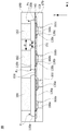
- FIG. 1 is a plan view of a semiconductor device according to a first embodiment of the present invention
- FIG. 2 is a cross-sectional view along the direction A-A of FIG.
- FIG. 3 is a cross-sectional view of a semiconductor device according to a second embodiment of the present invention.
- 4A and 4B are graphs illustrating changes in luminous flux and color purity according to widths of barrier ribs of a semiconductor device according to an embodiment
- FIG. 5 is a cross-sectional view of a semiconductor device according to a third exemplary embodiment of the present invention.
- FIG. 6 is a modification of FIG. 5,
- FIG. 7A to 7F are views illustrating a method of manufacturing a semiconductor device according to the third embodiment
- FIG. 8 is a cross-sectional view of a semiconductor device according to a fourth embodiment of the present invention.
- FIGS. 9A to 9D are views illustrating a method of manufacturing a semiconductor device according to the fourth embodiment.
- FIG. 10 is a cross-sectional view of a modification of the semiconductor device according to the fourth embodiment shown in FIG. 8.
- FIG. 11 is a cross-sectional view of a semiconductor device according to a fifth embodiment of the present invention.
- FIG. 12 is a sectional view of a semiconductor device according to a sixth embodiment of the present invention.
- FIG. 13 is a sectional view of a semiconductor device according to a seventh embodiment of the present invention.
- FIG. 14 is a plan view of a display device according to an exemplary embodiment.
- 15 is a diagram illustrating a state in which a semiconductor device and a circuit board are electrically connected.
- the semiconductor device may include various electronic devices such as a light emitting device and a light receiving device, and the light emitting device and the light receiving device may all include the first conductive semiconductor layers 110a, 110b, and 110c, the active layers 120a, 120b, and 120c, and the second devices. It may include a conductive semiconductor layer (130a, 130b, 130c).
- the semiconductor device according to the present embodiment may be a light emitting device.
- the light emitting device emits light by recombination of electrons and holes, and the wavelength of the light is determined by the energy band gap inherent in the material. Thus, the light emitted may vary depending on the composition of the material.
- FIG. 1 is a plan view of a semiconductor device according to a first exemplary embodiment of the present invention
- FIG. 2 is a cross-sectional view taken along the direction A-A of FIG. 1.
- the semiconductor device may include a plurality of light emitting parts P1, P2, and P3.
- the plurality of light emitting parts P1, P2, and P3 may emit light having the same or different wavelengths, respectively.
- the plurality of light emitting parts P1, P2, and P3 may be defined as areas that can be independently controlled. For example, only one of the first to third light emitting parts P1, P2, and P3 may be independently turned on by applying a current selectively among the plurality of light emitting parts P1, P2, and P3.
- the plurality of light emitting parts P1, P2, and P3 includes a first light emitting part P1 for emitting light of a first wavelength band, a second light emitting part P2 for emitting light of a second wavelength band, and a light of a third wavelength band. It may include a third light emitting unit (P3) for emitting.
- the first light emitting unit P1 may emit green light
- the second light emitting unit P2 and the third light emitting unit P3 may emit blue light, but are not limited thereto.
- the first light emitter P1 may emit blue light
- the second light emitter P2 and the third light emitter P3 may emit green light.
- all of the first to third light emitting parts P1, P2, and P3 may emit blue light.
- the first to third light emitting parts P1, P2, and P3 may emit light of different wavelength bands according to the injected current.
- the semiconductor device 1A may include a first electrode electrically connecting the first to third light emitting parts P1, P2, and P3 and the separated first conductive semiconductor layers 110a, 110b, and 110c. 151, a first bump electrode 150 connected to the first electrode 151, and a plurality of second bump electrodes 160a electrically connected to the second conductive semiconductors 130a, 130b, and 130c, respectively. 160b, 160c).
- the first bump electrode 150 and the second bump electrodes 160a, 160b, and 160c of the semiconductor device may be disposed under the plurality of light emitting parts P1, P2, and P3.
- the first bump electrodes 150 and the second bump electrodes 160a, 160b, and 160c are disposed below the second conductive semiconductor layers 130a, 130b, and 130c, but the present invention is not limited thereto.
- the first bump electrodes 150 and the second bump electrodes 160a, 160b, and 160c may be disposed on the first conductive semiconductor layers 110a, 110b, and 110c.
- the first to third light emitting units P1, P2, and P3 may include the first conductive semiconductor layers 110a, 110b, and 110c, the active layers 120a, 120b, and 120c, and the second conductive semiconductor layers 130a, 130b, and 130c).
- the first light emitting unit P1 may include a first conductive semiconductor layer 110a, an active layer 120a, and a second conductive semiconductor layer 130a
- the second light emitting unit P2 may include a first conductive layer.
- the third light emitting part P3 includes the first conductivity-type semiconductor layer 110c, the active layer 120c, and the second.
- the conductive semiconductor layer 130c may be included.
- the first conductive semiconductor layers 110a, 110b, and 110c of the first to third light emitting units P1, P2, and P3 may be disposed to have a narrower width toward the upper side, and the first to third light emitting units P1.
- the second conductivity-type semiconductor layers 130a, 130b, and 130c of the P2 and P3 may be disposed to have a smaller width as they go downward. That is, the first conductive semiconductor layers 110a, 110b and 110c and the second conductive semiconductor layers 130a, 130b and 130c may be made narrower in the opposite directions.
- the first conductive semiconductor layers 110a, 110b, and 110c may be formed of compound semiconductors such as group III-V and group II-VI, and may be doped with n-type dopants.
- a first conductive type semiconductor layer (110a, 110b, 110c) is having a compositional formula of In x Al y Ga 1 -x- y N (0 ⁇ x ⁇ 1, 0 ⁇ y ⁇ 1, 0 ⁇ x + y ⁇ 1) having a composition formula of a semiconductor material, or in x Al y Ga 1 -x- y P (0 ⁇ x ⁇ 1, 0 ⁇ y ⁇ 1, 0 ⁇ x + y ⁇ 1) can be formed of a semiconductor material.
- the n-type dopant may be selected from Si, Ge, Sn, Se, Te, and the like, but is not limited thereto.
- the active layers 120a, 120b, and 120c may have any one of a single well structure, a multi well structure, a single quantum well structure, a multi quantum well (MQW) structure, a quantum dot structure, or a quantum line structure.
- the structures of the active layers 120a, 120b, and 120c are not limited thereto.
- An active layer (120a, 120b, 120c) when formed into a quantum well structure for example, In x Al y Ga 1 -x- y N (0 ⁇ x ⁇ 1, 0 ⁇ y ⁇ 1, 0 ⁇ x + y ⁇ 1)
- a well layer having a compositional formula and a barrier layer having a compositional formula of In a Al b Ga 1 -a- b N (0 ⁇ a ⁇ 1, 0 ⁇ b ⁇ 1, 0 ⁇ a + b ⁇ 1) It may have a well structure.
- the active layers 120a, 120b, and 120c may have (Al p Ga 1 -p ) q In 1 - q P layers (where 0 ⁇ p ⁇ 1 and 0 ⁇ q ⁇ 1), respectively.
- the composition of the barrier layer (Al Ga 1 -p1 p1) q1 in 1 - q1 be a P layer (where, 0 ⁇ p1 ⁇ 1, 0 ⁇ q1 ⁇ 1), but the embodiment is not limited thereto.
- the active layers 120a, 120b, and 120c may be formed of one or more pair structures of InGaN / GaN, InGaN / InGaN, GaN / AlGaN, InAlGaN / GaN, GaAs (InGaAs) / AlGaAs, GaP (InGaP) / AlGaP.
- the well layer may be formed of a material having a band gap smaller than the band gap of the barrier layer.
- the active layers 120a, 120b, and 120c are electrons (or holes) injected through the first conductivity type semiconductor layers 110a, 110b, and 110c, and holes injected through the second conductivity type semiconductor layers 130a, 130b, and 130c. (Or electron) is the layer where it meets.
- the active layers 120a, 120b, and 120c may transition to low energy levels as electrons and holes recombine, and may generate light having a corresponding wavelength.
- the active layers 120a, 120b, and 120c of the first, second, and third light emitting parts P1, P2, and P3 may generate light in a blue wavelength band.
- the second conductive semiconductor layers 130a, 130b, and 130c may be implemented with compound semiconductors such as group III-V and group II-VI, and may be doped with p-type dopants.
- the second conductivity type semiconductor layer (130a, 130b, 130c) is having a compositional formula of In x Al y Ga 1 -x- y N (0 ⁇ x ⁇ 1, 0 ⁇ y ⁇ 1, 0 ⁇ x + y ⁇ 1) having a composition formula of a semiconductor material, or in x Al y Ga 1 -x- y P (0 ⁇ x ⁇ 1, 0 ⁇ y ⁇ 1, 0 ⁇ x + y ⁇ 1) can be formed of a semiconductor material.
- the second conductive semiconductor layers 130a, 130b, and 130c may be formed of a material selected from AlInN, AlGaAs, GaP, GaAs, GaAsP, and AlGaInP, but is not limited thereto.
- the p-type dopant may be selected from Mg, Zn, Ca, Sr, Ba, and the like, but is not limited thereto.
- the first to third light emitting parts P1, P2, and P3 may emit light in the blue wavelength band through the first conductivity type semiconductor layers 110a, 110b, and 110c.
- the first insulating layer 140 may be disposed under the first to third light emitting parts P1, P2, and P3.
- the first insulating layer 140 may be formed by selecting at least one selected from the group consisting of SiO 2 , Si x O y , Si 3 N 4 , SixNy, SiOxNy, Al 2 O 3 , TiO 2 , AlN, and the like. It is not limited.
- the first insulating layer 140 may electrically insulate the first electrode 151 from the second conductive semiconductor layers 130a, 130b and 130c and the active layers 120a, 120b and 120c.
- the first insulating layer 140 may be a distributed Bragg reflector (DBR) having a multilayer structure including a Si oxide or a Ti compound.
- DBR distributed Bragg reflector
- the present invention is not limited thereto, and the first insulating layer 140 may include various reflective structures.
- the first electrode 151 may be disposed between the separated first conductivity type semiconductor layers 110a, 110b, and 110c.
- the first electrode 151 may electrically connect the separated first conductive semiconductor layers 110a, 110b, and 110c.
- the first electrode 151 may be electrically connected to the first conductivity type semiconductor layers 110a, 110b, and 110c by passing through the first insulating layer 140.
- the first electrode 151 may be spaced apart from the second bump electrodes 160a, 160b and 160c.
- the first electrode 151 may electrically connect the first conductivity-type semiconductor layers 110a, 110b, and 110c of each light emitting structure.
- the first electrode 151 may be partially overlapped with the first conductivity type semiconductor layers 110a, 110b, and 110c to be electrically connected thereto.
- the first electrode 151 may be an ohmic electrode, but is not limited thereto.
- the first bump electrode 150 may be electrically connected to the first electrode 151. Accordingly, the first conductivity type semiconductor layers 110a, 110b, and 110c disposed to be spaced apart from each other may have a first shape. The bump electrode 150 may be electrically connected to the bump electrode 150. The first bump electrode 150 and the first electrode 151 may function as a common electrode, but are not limited thereto.
- the plurality of second bump electrodes 160a, 160b and 160c may be electrically connected to the second conductive semiconductor layers 130a, 130b and 130c.
- the 2-1 bump electrode 160a may be electrically connected to the 2-1 conductive semiconductor layer 130a
- the 2-2 bump electrode 160b may be the 2-2 conductive semiconductor layer 130b.
- the 2-3 bump electrode 160c may be electrically connected to the 2-3 conductive semiconductor layer 130c.
- the first bump electrodes 150 and the second bump electrodes 160a, 160b, and 160c are formed of metals such as Ag, Ni, Al, Rh, Pd, Ir, Ru, Mg, Zn, Pt, Au, Hf, Cu, and the like. Can be.
- the first bump electrode 150 and the second bump electrodes 160a, 160b, and 160c may be formed of one or a plurality of layers in which the conductive oxide film and the metal are mixed, but are not limited thereto.
- a reflective layer may be further disposed under the second conductive semiconductor layers 130a, 130b, and 130c, but embodiments are not limited thereto.
- Second electrodes 161a, 161b and 161c may be disposed between the plurality of second bump electrodes 160a, 160b and 160c and the second conductive semiconductor layers 130a, 130b and 130c.
- the present invention is not limited thereto, and the second bump electrodes 160a, 160b, and 160c may include a material in ohmic contact with the second conductive semiconductor layers 130a, 130b, and 130c.
- the support layer 170 includes the insulating layer 140, the first electrode 151, the first conductive semiconductor layers 110a, 110b, and 110c, the active layers 120a, 120b, and 120c, and the second conductive semiconductor layer 130a, It may be disposed under the semiconductor device to support the 130b, 130c.
- the support layer 170 may have low light transmittance and may serve as a light reflection layer and / or a light absorption layer.
- the support layer 170 may have a structure in which reflective particles are dispersed on a substrate.
- the substrate may be any one or more of epoxy resins, silicone resins, polyimide resins, urea resins, and acrylic resins.
- the polymer resin may be a silicone resin.
- the reflective particles may include inorganic particles such as TiO 2 or SiO 2 .
- the support layer may be an epoxy molding compound (EMC) or silicone molding compound (SMC) resin.
- the support layer 170 may include 10 to 50 wt%, or 15 to 30 wt% of inorganic particles. If the content of the particles is less than 10wt%, it is difficult to control the permeability to 20% or less, and if the content is more than 50wt%, the content of inorganic particles may be high and cracks may occur.
- the support layer 170 may have a thermal expansion coefficient (CTE) of 50 ppm / ° C or less.
- CTE thermal expansion coefficient
- the transmittance of the support layer 170 may be 20% or less.
- the semiconductor device may provide improved light emission efficiency.
- FIGS. 4A and 4B are graphs of changes in luminous flux and color purity according to widths of partition walls of semiconductor devices according to an exemplary embodiment.
- the semiconductor device 1B may include wavelength conversion layers 181, 182, and 183 and barrier ribs disposed on the first to third light emitting parts P1, P2, and P3. 190) may be further included.
- the wavelength conversion layers 181, 182, and 183 may convert wavelengths of light emitted from the first to third light emitting parts P1, P2, and P3.
- the first wavelength conversion layer 181 may convert light emitted from the first light emitting part P1 into green light
- the second wavelength conversion layer 182 may be emitted from the second light emitting part P2.
- the light may be converted into red light
- the third wavelength conversion layer 183 may convert light emitted from the third light emitting part P3 into blue light.
- the third wavelength conversion layer 183 may not change the wavelength or may not be disposed.
- the present disclosure is not limited thereto, and the first to third wavelength conversion layers 181, 182, and 183 may emit light of the blue (B) wavelength band emitted from the first to third light emitting parts P1, P2, and P3. It can also be absorbed and converted to light in the white (W) wavelength band.
- B blue
- W white
- the wavelength conversion layers 181, 182, and 183 may have a structure in which wavelength conversion particles are dispersed in a polymer resin selected from an epoxy resin, a silicone resin, a polyimide resin, a urea resin, an acrylic resin, and the like, but is not limited thereto.
- the wavelength conversion particle may include any one or more of a phosphor and a quantum dot (QD).
- QD quantum dot
- the phosphor may include a fluorescent material of any one of YAG-based, TAG-based, Silicate-based, Sulfide-based, or Nitride-based, but the embodiment is not limited to the type of phosphor.
- YAG and TAG-based fluorescent materials may be selected from (Y, Tb, Lu, Sc, La, Gd, Sm) 3 (Al, Ga, In, Si, Fe) 5 (O, S) 12 : Ce.
- Silicate-based fluorescent material may be selected from (Sr, Ba, Ca, Mg) 2 SiO 4 : (Eu, F, Cl).
- the sulfide-based fluorescent material can be selected from (Ca, Sr) S: Eu, (Sr, Ca, Ba) (Al, Ga) 2 S 4 : Eu, and the Nitride-based fluorescent material is (Sr, Ca, Si, Al , O) N: Eu (eg, CaAlSiN 4 : Eu ⁇ -SiAlON: Eu) or Ca- ⁇ SiAlON: Eu-based (Cax, My) (Si, Al) 12 (O, N) 16 .
- M is at least one of Eu, Tb, Yb or Er and may be selected from phosphor components satisfying 0.05 ⁇ (x + y) ⁇ 0.3, 0.02 ⁇ x ⁇ 0.27 and 0.03 ⁇ y ⁇ 0.3.
- the wavelength conversion layers 181, 182, and 183 may be separated by the partition wall 190 for each region overlapping the first to third light emitting parts P1, P2, and P3 in the vertical direction.
- the partition wall 190 may be disposed between the wavelength conversion layers 181, 182, and 183 and between the light emitting parts P1, P2, and P3.
- the partition wall 190 may include a light absorbing material, such as carbon black and graphite, or may include a reflecting material that reflects light.
- the partition wall 190 may have a structure in which reflective particles are dispersed on a substrate.
- the substrate may be any one or more of epoxy resins, silicone resins, polyimide resins, urea resins, and acrylic resins.
- the polymer resin may be a silicone resin.
- the reflective particles may include inorganic particles such as TiO 2 or SiO 2 , but are not limited thereto.
- the partition wall 190 may include 20 wt% or more of inorganic particles.
- the inorganic particles of the partition wall may be 20 wt% to 70 wt%.
- the reflectivity of the partition wall 190 is lowered, thereby lowering the color purity.
- the partition wall 190 may have cracks because the content of the polymer resin decreases when the inorganic particles exceed 70 wt%.
- the partition wall 190 may include a first region disposed between the wavelength conversion layers 181, 182, and 183, and a second region disposed between the first to third light emitting parts P1, P2, and P3. .
- the width d1 of the first region may be greater than the width d2 of the second region.
- the present invention is not limited thereto, and the width d1 of the first region and the width d2 of the second region may be the same.
- the widths d1 and d2 of the first area and the second area may be distances in a direction perpendicular to the thickness direction of the light emitting parts P1, P2, and P3 (the X-axis direction).
- the width d1 of the first region of the barrier rib 190 may be 10 ⁇ m or more.
- the width d1 of the first region may be 10 ⁇ m to 50 ⁇ m.
- the partition wall 190 may block color light emitted from the first to third light emitting parts P1, P2, and P3 to improve color purity.
- the partition wall 190 blocks the light emitted from the first to third light emitting parts P1, P2, and P3 to overlap and mix the light. You can prevent it.
- the width between the first to third light emitting parts P1, P2, and P3 may be widened, thereby increasing the size of the semiconductor device.
- the formation method of the partition 190 is not specifically limited.
- the partition wall 190 may be formed using photolithography, imprinting, roll-to-roll printing, inkjet printing, or the like.
- the width d1 of the first region may be greater than the maximum width d2 of the second region. Accordingly, the width in the X-axis direction of each of the first to third wavelength conversion layers 181, 182, and 183 may be smaller than the width of the first to third light emitting parts P1, P2, and P3. According to such a structure, the width
- the X-axis width of each of the first to third wavelength conversion layers 181, 182, and 183 may be 80% to 90% of the width of the first to third light emitting parts P1, P2, and P3. have.
- the luminous flux of the plurality of light emitting parts decreases slightly as the width of the first region increases, it may be confirmed that color purity is greatly improved. That is, when the width of the first region is 20 ⁇ m, the color purity is improved by 102%, when the width of the first region is 30 ⁇ m, by 105%, and when the width of the first region is 50 ⁇ m by 106%.
- FIG. 5 is a cross-sectional view of a semiconductor device according to a third exemplary embodiment of the present invention
- FIG. 6 is a modification of FIG. 5.
- the semiconductor device 1C may include the wavelength conversion layers 181, 182, and 183 and the color filter layer 220 disposed on the barrier rib 190.
- the color filter layer 220 may include a plurality of color filters 221, 222, and 223 and a black matrix 224.
- the first to third color filters 221, 222, and 223 may be disposed on the color filter layer 220.
- the first color filter 221 may be a green filter
- the second color filter 222 may be a red filter
- the third color filter 223 may be a blue filter.
- the plurality of color filters 221, 222, and 223 may be manufactured by mixing green / red / blue pigment with acrylic resin such as Methylmethacrylate-Butadiene-Styrene (MBS).
- acrylic resin such as Methylmethacrylate-Butadiene-Styrene (MBS).
- MBS Methylmethacrylate-Butadiene-Styrene
- the color filter layer 220 may be formed by coating, exposing, developing, and curing (firing) the pigment composition dispersed in the photoresist.
- the color filter layer 220 may improve color purity of the light converted by the wavelength conversion layers 181, 182, and 183.
- the first color filter 221 may block light other than the green light converted by the first wavelength conversion layer 181 to improve the color purity of the green light.
- the color filter layer 220 may emit light in the white (W) wavelength band.
- the light may be separated into light of the blue (B), green (G), and red (R) wavelength bands.
- the color filter layer 220 may include a black matrix 224 disposed between the first to third color filters 221, 222, and 223.
- the present invention is not necessarily limited thereto, and the structure is not particularly limited as long as the structure is arranged between the first to third color filters 221, 222, and 223 to be partitioned.
- the thickness of the black matrix 224 may be 5 ⁇ m to 55 ⁇ m. If the thickness is smaller than 5 ⁇ m, it may be too thin to partition the first to third color filters 221, 222, and 223. If the thickness is larger than 55 ⁇ m, the overall filter may have a thick thickness. However, the thickness of the black matrix 224 is not necessarily limited thereto.
- the width of the black matrix 224 may have a range of ⁇ 5 ⁇ m of the width d1 of the first region of the partition 190 disposed below the black matrix 224.
- the width of the black matrix 224 may be 5 ⁇ m to 55 ⁇ m.
- the first intermediate layer 210 may be disposed between the color filter layer 220 and the wavelength conversion layers 181, 182, and 183 to bond them.
- the color filters 221, 222, and 223 may use acrylic resin as the main raw material
- the partition walls and the wavelength conversion layers 181, 182, and 183 may use silicone resin as the main raw material.
- the acrylic resin and the silicone resin have poor adhesion due to the difference in physical properties, it may not be easy to fabricate the color filters 221, 222, and 223 directly on the wavelength conversion layers 181, 182, and 183.
- the first intermediate layer 210 may include an oxide or nitride as an inorganic material.
- the first intermediate layer 210 may be formed of indium tin oxide (ITO), indium zinc oxide (IZO), indium zinc tin oxide (IZTO), indium aluminum zinc oxide (IAZO), indium gallium zinc oxide (IGZO), or IGTO.
- the present invention is not limited thereto, and the first intermediate layer 210 may be selected without limitation as long as the material has excellent adhesion to both the acrylic resin and the silicone resin.
- the thickness of the first intermediate layer 210 may be 5 nm to 1,000 nm, or 40 nm to 200 nm. When the thickness is smaller than 5 nm, it is difficult to prevent the acrylic resin from diffusing into the phosphor, and when the thickness is larger than 1000 nm, the transmittance is smaller than 70%, resulting in a decrease in the luminous flux.
- the total thickness L 1 of the barrier rib 190, the first intermediate layer 210, the color filter layer 220, and the encapsulation layer 230 may be 30 ⁇ m to 100 ⁇ m.
- the wavelength conversion layers 181, 182, and 183 may be formed in the wavelength conversion layers 181, 182, and 183.
- the small number of particles can result in less color conversion and can be difficult to process.
- the thickness means the distance in the Y-axis direction.
- a second intermediate layer 240 may be disposed between the first intermediate layer 210 and the wavelength conversion layers 181, 182, and 183.
- the wavelength conversion layers 181, 182, and 183 may not have a flat surface because phosphor particles are dispersed by a process or in a resin. Therefore, when the color filter layer is formed on the surfaces of the wavelength conversion layers 181, 182, and 183, there is a problem that reliability is lowered.
- the first intermediate layer 210 may be disposed on the second intermediate layer 240 to provide a flat surface.
- the configuration of the second intermediate layer 240 is not necessarily limited thereto and may be omitted.
- the second intermediate layer 240 may be omitted.
- the surface roughness of the first intermediate layer 210 may be determined by the surface roughness of the wavelength conversion layers 181, 182, and 183 and the partition wall 190.
- a leveling or polishing process may be performed to control the surface roughness of the wavelength conversion layers 181, 182, and 183 and the partition wall 190.
- the second intermediate layer 240 may include the same material for adhesion to the wavelength conversion layers 181, 182, and 183.
- the second intermediate layer 240 and the wavelength conversion layers 181, 182, and 183 may all include a silicone resin.
- the thickness of the second intermediate layer 240 may be 3,000 nm to 20,000 nm. If the thickness of the second intermediate layer 240 is smaller than 3,000 nm, the planarization of the surface may be poor. If the thickness of the second intermediate layer 240 is greater than 20,000 nm, the light transmittance may be reduced. Therefore, the thickness ratio of the first intermediate layer 210 and the second intermediate layer 240 may be 1: 4000 to 1: 3.
- the encapsulation layer 230 may be disposed on the color filter layer 220.
- the encapsulation layer 230 is disposed on the color filter layer 220 to cover the pixel and the semiconductor element, and includes a plurality of light emitting parts P1, P2, and P3, the wavelength conversion layers 181, 182, and 183, and the partition wall 190. Can protect.
- the encapsulation layer 230 is made of heat and / or photocurable resin and coated on the color filter layer 220 in a liquid state, and may be cured by a curing process using heat and / or light. In this case, the encapsulation layer 230 may also serve to buffer external pressing.
- FIG. 7A to 7F are views illustrating a method of manufacturing a semiconductor device according to the third embodiment.
- the first conductive semiconductor layer 110, the active layer 120, and the second conductive semiconductor layer 130 may be sequentially formed on the substrate 1.
- the substrate 1 may be formed of a material selected from sapphire (Al 2 O 3 ), SiC, GaAs, GaN, ZnO, Si, GaP, InP, and Ge, but is not limited thereto.
- a buffer layer (not shown) may be further provided between the first conductivity-type semiconductor layer 110 and the substrate 1.
- the buffer layer may mitigate lattice mismatch between the first conductive semiconductor layer 110, the active layers 120 and 120, and the second conductive semiconductor layer 130 and the substrate 1.
- the buffer layer may have a form in which Group III and Group V elements are combined or include any one of GaN, InN, AlN, InGaN, AlGaN, InAlGaN, and AlInN.
- the dopant may be doped in the buffer layer, but is not limited thereto.
- the first conductive semiconductor layer 110, the active layer 120, and the second conductive semiconductor layer 130 may be formed of metal organic chemical vapor deposition (MOCVD), chemical vapor deposition (CVD), and plasma.
- MOCVD metal organic chemical vapor deposition
- CVD chemical vapor deposition
- plasma Plasma-Enhanced Chemical Vapor Deposition
- MBE Molecular Beam Epitaxy
- HVPE Hydride Vapor Phase Epitaxy
- Sputtering It is possible to, but not limited to.
- the first insulating layer 140, the first electrode 151, and the second electrodes 161a, 161b, and 161c may be formed on the second conductive semiconductor layer 130. Subsequently, after the support layer 170 is formed, the first bump electrodes 150 and the second bump electrodes 160a, 160b, and 160c may be penetrated.
- the present invention is not limited thereto, and the first bump electrode 150 and the second bump electrodes 160a, 160b, and 160c may be formed, and then the support layer 170 may be formed.
- the second conductive semiconductor layers 130a, 160b, and 160c and the active layers 120a, 120b, and 120c may be mesa-etched to be separated from each other. Therefore, the second conductivity-type semiconductor layers 130a, 160b and 160c and the active layers 120a, 120b and 120c may be formed to be narrow in a direction away from the substrate 1.
- the substrate 1 may be removed.
- the substrate 1 may use a laser lift off (LLO) method, but is not limited thereto.
- LLO laser lift off
- the first conductivity type semiconductor layer 110 may be separated in units of the light emitting units P1, P2, and P3. Therefore, the first conductivity type semiconductor layer 110 may be formed to have a narrow width in the opposite direction to the second conductivity type semiconductor layer 130 during the mesa etching process.
- the wavelength conversion layers 181, 182, and 183 and the partition wall 190 may be formed on the first conductivity type semiconductor layer 110.
- the wavelength conversion layers 181, 182, and 183 may be formed first, and then the barrier rib 190 may be formed, but the present invention is not limited thereto.
- the barrier rib 190 is formed first, and then the through-hole is formed to form a wavelength therein.
- the conversion layers 181, 182, and 183 may be formed.
- the first intermediate layer 210 may be formed on the wavelength conversion layers 181, 182, and 183, and the first to third color filters 221, 222, and 223 may be formed thereon.
- the black matrix may be formed first to be aligned with the wavelength conversion layers 181, 182, and 183, and then the first to third color filters 221, 222, and 223 may be formed, but is not limited thereto.
- the green pigment is coated on the entire surface by a spin coating method or a bar coating method, and the mask process is performed to apply a green pigment to a region corresponding to the first wavelength conversion layer 181.
- One color filter 221 may be formed.
- the red pigment is coated on the entire surface by a spin coating method or a bar coating method, and a mask process is performed to form a second pigment in a region corresponding to the second wavelength conversion layer 182.
- the color filter 222 may be formed.
- the blue pigment is coated on the entire surface by a spin coating method or a bar coating method, and a mask process is performed to form a third pigment in a region corresponding to the third wavelength conversion layer 183.
- the color filter 223 may be formed. Thereafter, as shown in FIG. 7F, the encapsulation layer 230 may be formed on the color filter layer 220.
- FIG. 8 is a cross-sectional view of a semiconductor device according to a fourth exemplary embodiment of the present invention.
- the semiconductor device 1D may include a blocking layer 200 disposed between the wavelength conversion layers 181, 182, and 183, and between the first to third light emitting parts P1, P2, and P3. It may further include.
- the blocking layer 200 may also be disposed on the first insulating layer 140.
- the blocking layer 200 may block light emitted from the first to third light emitting parts P1, P2, and P3 to be adjacent to the wavelength conversion layers 181, 182, and 183.
- the blocking layer 200 may prevent the light emitted from the first light emitting part P1 from entering the second wavelength conversion layer 182.
- the blocking layer 200 may prevent overlapping and mixing of light.
- the blocking layer 200 may include a metal.
- the blocking layer 200 may include light reflecting metal to reflect light moving to adjacent wavelength converting layers 181, 182, and 183.
- the metal may include Ag, Ni, Ti, Al, but is not limited thereto.
- the width d3 of the blocking layer 200 may be 20 nm or more. Preferably, the width d3 of the blocking layer 200 may be 100 nm to 1000 nm. When the width d3 of the blocking layer 200 is smaller than 100 nm, fixing of the blocking layer 200 may be difficult, and thus surface roughness may increase. In addition, when the width d3 of the blocking layer 200 is greater than 1000 nm, peeling may occur due to stress due to weight.
- the blocking layer 200 may be formed by deposition of metal, but is not limited thereto.
- the color filter layer 220 may include a plurality of color filters 221, 222, and 223 and a black matrix 224.
- the first to third color filters 221, 222, and 223 may be disposed on the color filter layer 220.
- the first color filter 221 may be a green filter
- the second color filter 222 may be a red filter
- the third color filter 223 may be a blue filter.
- the first intermediate layer 210 may be disposed between the color filter layer 220 and the wavelength conversion layers 181, 182, and 183 to bond them.
- the features described with reference to FIG. 5 may be applied to the color filter layer 220 and the first intermediate layer 210 as they are.
- the second intermediate layer of FIG. 6 may be further disposed.
- 9A to 9D are views illustrating a method of manufacturing a semiconductor device according to the fourth embodiment.
- the manufacturing process described with reference to FIGS. 7A to 7C may be applied as it is. That is, after the substrate is removed, the first conductivity-type semiconductor layer 110 may be separated into units of the light emitting units P1, P2, and P3. Therefore, the first conductivity type semiconductor layer 110 may be formed to have a narrow width in the opposite direction to the second conductivity type semiconductor layer 130 during the mesa etching process.
- the wavelength conversion layers 181, 182, and 183 and the photosensitive layer S may be formed on the first conductive semiconductor layer 110.
- the wavelength conversion layers 181, 182, and 183 may be formed first, and then the photosensitive layer S may be formed.
- the present invention is not limited thereto, and the photosensitive layer S is first formed, and then a through hole is formed.
- the wavelength conversion layers 181, 182, and 183 may be formed therein.
- the blocking layer 200 is disposed between the wavelength conversion layers 181, 182, and 183, the first to third light emitting parts P1, P2, and P3, and the first electrode 151 and the partition wall 190. This can be formed.
- the blocking layer 200 may be deposited after removing the photosensitive layer S.
- the blocking layer 200 may be formed using a method such as metal organic chemical vapor deposition (MOCVD), chemical vapor deposition (CVD), sputtering, or the like, but is not limited thereto.
- MOCVD metal organic chemical vapor deposition
- CVD chemical vapor deposition
- sputtering or the like, but is not limited thereto.
- the blocking layer 200 may be formed, and the partition wall 190 may be formed on the blocking layer 200.
- the wavelength conversion layers 181, 182, and 183, the barrier ribs 190, and the barrier layer 200 may be exposed to the top surface of the wavelength conversion layers 181, 182, and 183 and the barrier ribs 190, respectively. And a part of the blocking layer 200 may be removed.
- the removal method may apply a leveling and polishing process, but is not necessarily limited thereto.
- FIG. 10 is a cross-sectional view of a modified example of the semiconductor device according to the fourth embodiment shown in FIG. 8.
- the blocking layer 200 of the semiconductor device 1D ′ may be formed between the wavelength conversion layers 181, 182, and 183, and the first to third light emitting parts P1, P2, and P3 and the partition wall 190. Can be placed in. In this case, the first insulating layer 140 may be exposed between the blocking layers 200.
- the blocking layer 200 may block light emitted from the first to third light emitting parts P1, P2, and P3 to be adjacent to the wavelength conversion layers 181, 182, and 183. By such a configuration, the blocking layer 200 can provide overlapping and mixing of light.
- the blocking layer 200 may be equally applicable to the above description.
- FIG. 11 is a sectional view of a semiconductor device according to a fifth embodiment of the present invention.
- the semiconductor device 1E may be electrically connected to the first to third light emitting parts P1, P2, and P3 and the first conductive semiconductor layers 110a, 110b, and 110c spaced apart from each other.
- the first bump electrodes 150a, 150b and 150c, the second electrode 162 electrically connecting the separated second conductive semiconductor layers 130a, 130b and 130c, and the second electrode 162 are electrically connected to each other. It may include two bump electrodes 160.
- the first bump electrodes 150a, 150b, and 150c are electrically connected to the first conductive semiconductor layers 110a, 110b, and 110c, respectively, and the second bump electrodes 160 may be The second conductive semiconductor layers 130a, 130b, and 130c may be electrically connected to each other through the second electrode 162.
- the second electrode 162 may be disposed between the second conductive semiconductor layers 130a, 130b, and 130c spaced apart from the first to third light emitting parts P1, P2, and P3.
- the second electrode 162 may electrically connect the second conductive semiconductor layers 130a, 130b, and 130c spaced apart from each other.
- first insulating layer 140 may be disposed under the first to third light emitting parts P1, P2, and P3.
- the reflective electrode 161 may be disposed under the second conductive semiconductor layers 130a, 130b, and 130c.
- the first conductive semiconductor layers 110a, 110b, 110c and the first bump electrodes 150a, 150b, and 150c of the first to third light emitting parts P1, P2, and P3 may respectively be provided. Electrodes 151a, 151b, and 151c may be disposed.
- the reflective electrode 161 is formed of a material having high reflectivity, such as Ag, Ni, Al, Rh, Pd, Ir, Ru, Mg, Zn, Pt, Au, and Hf, or the material having high reflectance and IZO, IZTO, IAZO Conductive materials such as IGZO, IGTO, AZO, ATO, etc. may be mixed and formed in a single layer or multiple layers, without being limited thereto.
- the second electrode 162 may be disposed between the reflective electrodes 161 to electrically connect the second conductive semiconductor layers 130a, 130b, and 130c to the second bump electrode 160.
- the second electrode 162 may serve as a common electrode for applying power to the first to third light emitting parts P1, P2, and P3.
- the first insulating layer 140 may be disposed to cover lower portions of the first to third light emitting parts P1, P2, and P3.
- the second insulating layer 141 may cover a portion of the first electrodes 151a, 151b, and 151c, a portion of the reflective electrode 161, and an entirety of the second electrode 162.
- At least one of the first insulating layer 140 and the second insulating layer 141 may be formed of SiO 2 , Si x O y , Si 3 N 4 , SixNy, SiOxNy, Al 2 O 3 , TiO 2 , AlN, or the like. It may be selected and formed, but is not limited thereto.
- the first insulating layer 140 may be a distributed Bragg reflector (DBR) having a multilayer structure including a Si oxide or a Ti compound.
- DBR distributed Bragg reflector
- the present invention is not limited thereto, and the first insulating layer 140 may include various reflective structures.
- the support layer 170 may be disposed under the plurality of light emitting parts P1, P2, and P3 to support the plurality of light emitting parts P1, P2, and P3 and the second electrode 162.
- the support layer 170 may have low light transmittance and may serve as a light reflection layer and / or a light absorption layer.
- the support layer 170 may have a structure in which reflective particles are dispersed on a substrate.
- the substrate may be any one or more of a light transmissive epoxy resin, a silicone resin, a polyimide resin, a urea resin, and an acrylic resin.
- the polymer resin may be a silicone resin.
- the reflective particles may include inorganic particles such as TiO 2 or SiO 2 .
- the support layer may be an epoxy molding compound (EMC) or silicone molding compound (SMC) resin.
- the support layer 170 may include 10 to 50 wt%, or 15 to 30 wt% of inorganic particles. If the content of the particles is less than 10wt%, it is difficult to control the permeability to 20% or less, and if the content is more than 50wt%, the content of inorganic particles may be high and cracks may occur.
- the support layer 170 may have a thermal expansion coefficient (CTE) of 50 ppm / ° C or less.
- CTE thermal expansion coefficient
- the transmittance of the support layer 170 may be 20% or less.
- the semiconductor device may provide improved light emission efficiency.
- the first bump electrodes 150a, 150b and 150c may be electrically connected to the first electrodes 151a, 151b and 151c through the support layer 170.
- the second bump electrode 160 may be electrically connected to the reflective electrode 161 through the support layer 170.
- the reflective electrodes 161 may be electrically connected to each other by the second electrode 162.
- the present invention is not limited thereto.
- the second bump electrode 160 may include the second conductive semiconductor layers 130a, 130b, and 130c of the first to third light emitting parts P1, P2, and P3 through the reflective electrode 161 and the second electrode 162. ) Can be electrically connected.
- FIG. 12 is a cross-sectional view of a semiconductor device according to a sixth embodiment of the present invention
- FIG. 13 is a cross-sectional view of a semiconductor device according to a seventh embodiment of the present invention.
- the semiconductor device 1F may include wavelength conversion layers 181, 182, and 183 and barrier ribs 190 disposed on the first to third light emitting parts P1, P2, and P3. It may further include.
- the wavelength conversion layers 181, 182, and 183 may convert wavelengths of light emitted from the first to third light emitting parts P1, P2, and P3.
- the first wavelength conversion layer 181 may convert light emitted from the first light emitting part P1 into green light
- the second wavelength conversion layer 182 may be emitted from the second light emitting part P2.
- the light may be converted into red light
- the third wavelength conversion layer 183 may convert light emitted from the third light emitting part P3 into blue light.
- the third wavelength conversion layer 183 may not change the wavelength.
- the present disclosure is not limited thereto, and the first to third wavelength conversion layers 181, 182, and 183 may emit light of the blue (B) wavelength band emitted from the first to third light emitting parts P1, P2, and P3. It can also be absorbed and converted to light in the white (W) wavelength band.
- B blue
- W white
- the wavelength conversion layers 181, 182, and 183 may have a structure in which wavelength conversion particles are dispersed in a polymer resin selected from a transparent epoxy resin, a silicone resin, a polyimide resin, a urea resin, an acrylic resin, and the like, but is not limited thereto.
- the wavelength conversion particle may include any one or more of a phosphor and a quantum dot (QD).
- QD quantum dot
- the phosphor may include a fluorescent material of any one of YAG-based, TAG-based, Silicate-based, Sulfide-based, or Nitride-based, but the embodiment is not limited to the type of phosphor.
- YAG and TAG-based fluorescent materials may be selected from (Y, Tb, Lu, Sc, La, Gd, Sm) 3 (Al, Ga, In, Si, Fe) 5 (O, S) 12 : Ce.
- Silicate-based fluorescent material may be selected from (Sr, Ba, Ca, Mg) 2 SiO 4 : (Eu, F, Cl).
- the sulfide-based fluorescent material can be selected from (Ca, Sr) S: Eu, (Sr, Ca, Ba) (Al, Ga) 2 S 4 : Eu, and the Nitride-based fluorescent material is (Sr, Ca, Si, Al , O) N: Eu (eg, CaAlSiN 4 : Eu ⁇ -SiAlON: Eu) or Ca- ⁇ SiAlON: Eu-based (Cax, My) (Si, Al) 12 (O, N) 16 .
- M is at least one of Eu, Tb, Yb or Er and may be selected from phosphor components satisfying 0.05 ⁇ (x + y) ⁇ 0.3, 0.02 ⁇ x ⁇ 0.27 and 0.03 ⁇ y ⁇ 0.3.
- the wavelength conversion layers 181, 182, and 183 may be separated by the partition wall 190 for each region overlapping the first to third light emitting parts P1, P2, and P3 in the vertical direction.
- the partition wall 190 may be disposed between the wavelength conversion layers 181, 182, and 183 and between the light emitting parts P1, P2, and P3.
- the partition wall 190 may include a light absorbing material, such as carbon black and graphite, or may include a reflecting material that reflects light.
- the partition wall 190 may have a structure in which reflective particles are dispersed on a substrate.
- the substrate may be any one or more of epoxy resins, silicone resins, polyimide resins, urea resins, and acrylic resins.
- the polymer resin may be a silicone resin.
- the reflective particles may include inorganic particles such as TiO 2 or SiO 2 , but are not limited thereto.
- the partition wall 190 may include 20 wt% or more of inorganic particles.
- the inorganic particles of the partition wall may be 20 wt% to 70 wt%.
- the reflectivity of the partition wall 190 is lowered, thereby lowering the color purity.
- the partition 190 may generate cracks when the inorganic particles exceed 70 wt%.
- the partition wall 190 may include a first region disposed between the wavelength conversion layers 181, 182, and 183, and a second region disposed between the first to third light emitting parts P1, P2, and P3. .
- the description of the partition wall 190 may be applied in the same manner to the above.
- the semiconductor device 1G may include the wavelength conversion layers 181, 182, and 183 and the color filter layer 220 disposed on the partition wall 190.
- first to third color filters 221, 222, and 223 may be disposed.
- the first color filter 221 may be a green filter
- the second color filter 222 may be a red filter
- the third color filter 223 may be a blue filter.
- the color filter layer 220 may be manufactured by mixing green / red / blue pigments with an acrylic resin such as Methylmethacrylate-Butadiene-Styrene (MBS).
- MBS Methylmethacrylate-Butadiene-Styrene
- the color filter layer 220 may be formed by coating, exposing, developing, and curing (firing) the pigment composition dispersed in the photoresist.
- the color filter layer 220 may improve color purity of the light converted by the wavelength conversion layers 181, 182, and 183.
- the first color filter 221 may block light other than the green light converted by the first wavelength conversion layer 181 to improve the color purity of the green light.
- the color filter layer 220 may emit light in the white (W) wavelength band.
- the light may be separated into light of the blue (B), green (G), and red (R) wavelength bands.
- the color filter layer 220 may include a black matrix 224 disposed between the first to third color filters 221, 222, and 223.
- the first intermediate layer 210 may be disposed between the color filter layer 220 and the wavelength conversion layers 181, 182, and 183.
- the color filter layer 220 may use acrylic resin as the main raw material, and the partition walls and the wavelength conversion layers 181, 182, and 183 may use silicone resin as the main raw material.
- the adhesion between the acrylic resin and the silicone resin is poor, it may not be easy to fabricate the color filter layer 220 directly on the wavelength conversion layers 181, 182, and 183.
- the first intermediate layer 210 may include an oxide or nitride as an inorganic material.
- the first intermediate layer 210 may include ITO, ZnO, AZO, and SiO 2 .
- the material of the first intermediate layer 210 is not necessarily limited thereto, and a material having excellent adhesion to both the acrylic resin and the silicone resin may be selected.
- the thickness of the first intermediate layer 210 may be 5 nm to 1000 nm, or 40 nm to 200 nm. When the thickness is smaller than 5 nm, it is difficult to prevent the acrylic resin from diffusing into the phosphor, and when the thickness is larger than 1000 nm, the transmittance is smaller than 70%, resulting in a decrease in the luminous flux.
- a second intermediate layer may be disposed between the first intermediate layer 210 and the wavelength conversion layers 181, 182, and 183.
- the encapsulation layer 230 may be disposed on the color filter layer 220.
- the encapsulation layer 230 is disposed on the color filter layer 220 to cover the pixel and the semiconductor element, and includes a plurality of light emitting parts P1, P2, and P3, the wavelength conversion layers 181, 182, and 183, and the partition wall 190. Can protect.
- the encapsulation layer 230 is made of heat and / or photocurable resin and coated on the color filter layer 220 in a liquid state, and may be cured by a curing process using heat and / or light. At this time, the encapsulation layer 230 also serves to buffer the external pressing.
- FIG. 14 is a plan view of a display device according to an exemplary embodiment
- FIG. 15 is a view illustrating a state in which a semiconductor device and a circuit board are electrically connected.
- the display device includes a panel 40 including a plurality of pixel regions defined as regions in which the common wiring 41 and the driving wiring 42 cross each other, and semiconductor devices disposed in each pixel region.
- the first driver 30 applies the drive signal to the common wire 41
- the second driver 20 applies the drive signal to the drive wire 42
- the first driver 30 and the second driver 20 may include a controller 50 for controlling).
- the second partition wall 46 disposed on the panel 40 may be disposed between the semiconductor elements disposed in each pixel region to support the semiconductor element, the common wiring 41, the driving wiring 42, and the like. Therefore, even if the panel 44 becomes large in area, disconnection of the common wiring 41 and the driving wiring 42 can be prevented.
- the second partition wall 46 may include a material such as carbon black, graphite, or the like, and may prevent light leakage between adjacent pixel areas, but is not limited thereto.
- the common wire 41 may be electrically connected to the first electrode 150 of the semiconductor device.
- the first, second, and third driving wirings 43, 44, and 45 are respectively connected to the second electrodes 160a, 160b, and 160c of the first, second, and third light emitting parts P1, P2, and P3. Can be electrically connected.
- the common wiring 41 and the driving wiring 42 may have a structure separated by at least one insulating layer therebetween, but are not limited thereto.
- the first and second insulating films 1a and 1b are illustrated.
- the semiconductor device may be disposed for each pixel area of the panel 40.
- One semiconductor element may function as a pixel of the display device.
- the first to third light emitting parts P1, P2, and P3 of the semiconductor device may function as first, second, and third subpixels.
- the first light emitting unit P1 may function as a blue subpixel
- the second light emitting unit P2 may function as a green subpixel
- the third light emitting unit P3 may be a red subpixel.
- Can function. Therefore, white light may be realized by mixing light of the blue, green, and red wavelength bands emitted from one semiconductor device as described above.
- the semiconductor device may be disposed in a chip scale package (CSP) on a substrate.
- CSP chip scale package
- the controller 50 may output control signals to the first and second drivers 30 and 20 to selectively apply power to the common wire 41 and the driving wire 42. Accordingly, the first to third light emitting parts P1, P2, and P3 of the semiconductor device may be individually controlled.
- a display device includes a semiconductor device including two or more light emitting devices packaged through an additional packaging process such as die-bonding and wire bonding. Can be placed. Therefore, the general display device needs to consider the packaging area, and thus the light emitting efficiency is low because the area of the panel that actually emits light is narrow.
- a chip level semiconductor device is disposed in a pixel area, and the first, second, and third light emitting parts P1, P2, and P3 of the semiconductor device may include the first, second, and third R, G, and B regions. It can function as a third sub-pixel. Therefore, it is not necessary to package the first to third light emitting parts P1, P2, and P3 serving as the first to third subpixels by additional processes such as die-bonding and wire bonding. As a result, an area for performing wire bonding or the like may be removed, thereby reducing the width between the first to third light emitting parts P1, P2, and P3 of the semiconductor device. That is, the pitch widths of the subpixels and the pixel areas may be reduced, thereby improving pixel density and resolution of the display device.
- the semiconductor device of the embodiment may secure the pad area described above. no need. Therefore, the light emitting efficiency is high, and as described above, the width between the first to third light emitting parts P1, P2, and P3 may be reduced, thereby reducing the size of the semiconductor device.
- SD Standard Definition
- HD High definition
- FHD Full HD
- UH Ultra HD
- the display device of the embodiment can be applied to an electronic display board or a TV having a diagonal size of 100 inches or more. This is because the semiconductor device according to the embodiment functions as each pixel as described above, so that power consumption is low and long life can be achieved at low maintenance costs.
Abstract
실시 예는, 복수 개의 발광부; 상기 복수 개의 발광부 상에 각각 배치되는 복수 개의 파장 변환층; 상기 복수 개의 발광부 사이, 및 상기 복수 개의 파장 변환층 사이에 배치되는 격벽; 상기 복수 개의 파장 변환층 상에 각각 배치되는 복수 개의 컬러필터; 및 상기 복수 개의 컬러필터 사이에 배치되는 블랙 매트릭스를 포함하는 반도체 소자를 개시한다.
Description
실시 예는 반도체 소자 및 이를 포함하는 표시장치에 관한 것이다.
발광 다이오드(Light Emitting Diode: LED)는 전류가 인가되면 광을 방출하는 발광 소자 중 하나이다. 발광 다이오드는 저 전압으로 고효율의 광을 방출할 수 있어 에너지 절감 효과가 뛰어나다. 최근, 발광 다이오드의 휘도 문제가 크게 개선되어, 액정표시장치의 백라이트 유닛(Backlight Unit), 전광판, 표시기, 가전 제품 등과 같은 각종 기기에 적용되고 있다.
일반적인 액정표시장치는 발광 다이오드로부터 방출된 광과 액정의 투과율을 제어하여 컬러필터를 통과하는 빛으로 이미지 또는 영상을 표시한다. 최근에는 HD 이상의 고화질 및 대 화면의 표시장치가 요구되고 있으나, 일반적으로 주로 사용되고 있는 복잡한 구성들을 갖는 액정표시장치 및 유기전계 표시장치는 수율 및 비용에 의해 고화질의 대화면 표시장치를 구현하기에 어려움이 있다.
실시 예는 색순도가 향상된 반도체 소자를 제공한다.
실시 예는 광도가 향상된 반도체 소자를 제공한다.
실시 예는 개별적으로 구동되는 제1 내지 제3 발광부를 포함하는 칩 레벨의 발광 소자가 표시 장치의 픽셀로 제공될 수 있다. 이 때, 제1 내지 제3 발광부가 픽셀의 각 서브 픽셀로 기능하여 고해상도의 대형 표시 장치를 구현할 수 있다.
실시 예에서 해결하고자 하는 과제는 이에 한정 되는 것은 아니며, 아래에서 설명하는 과제의 해결수단이나 실시형태로부터 파악될 수 있는 목적이나 효과도 포함된다고 할 것이다.
본 발명의 일 실시 예에 따른 반도체 소자는 복수 개의 발광부를 포함하는; 상기 복수 개의 발광부 상에 각각 배치되는 복수 개의 파장 변환층; 상기 복수 개의 발광부 사이, 및 상기 복수 개의 파장 변환층 사이에 배치되는 격벽 및 상기 복수 개의 파장 변환층 상에 각각 배치되는 복수 개의 컬러필터; 및 상기 복수 개의 컬러필터 사이에 배치되는 블랙 매트릭스를 포함한다.
상기 복수 개의 파장 변환층 사이의 폭은 상기 복수 개의 발광부 사이의 최대 폭보다 클 수 있다.
상기 각각의 발광부는, 제1 도전형 반도체층, 제2 도전형 반도체층, 및 상기 제1 도전형 반도체층과 상기 제2 도전형 반도체층 사이에 배치되는 활성층을 포함할 수 있다.
상기 복수 개의 발광부의 상기 제1 도전형 반도체층의 폭은 상기 파장 변환층에 가까워질수록 좁아질 수 있다.
상기 복수 개의 발광부의 상기 제2 도전형 반도체층의 폭은 상기 파장 변환층에 가까워질수록 커질 수 있다.
상기 복수 개의 발광부에 공통적으로 연결되는 제1 범프 전극; 상기 복수 개의 발광부에 각각 전기적으로 연결되는 복수 개의 제2 범프 전극; 및 상기 복수 개의 발광부의 제1 도전형 반도체층을 전기적으로 연결하는 제2 전극을 포함할 수 있다.
상기 복수 개의 발광부의 하부를 덮는 제1 절연층을 더 포함할 수 있다.
상기 제1 전극은 상기 제1 절연층을 관통하여 상기 제1 도전형 반도체층과 전기적으로 연결될 수 있다.
상기 제1 전극은 상기 제1 범프 전극과 전기적으로 연결될 수 있다.
상기 복수 개의 발광부에 각각 전기적으로 연결되는 복수 개의 제1 범프 전극; 상기 복수 개의 발광부에 공통적으로 연결되는 제2 범프 전극; 및 상기 복수 개의 발광부의 제2 도전형 반도체층을 전기적으로 연결하는 제2 전극을 포함할 수 있다.
상기 제2 전극은 상기 제2 범프 전극과 전기적으로 연결될 수 있다.
상기 복수 개의 발광부의 하부를 덮는 제1 절연층을 더 포함할 수 있다.
상기 제1 절연층을 관통하고, 상기 복수 개의 발광부의 제2 도전형 반도체층 하부에 각각 배치되는 복수 개의 반사 전극을 더 포함하고, 상기 제2 전극은 상기 복수 개의 반사 전극을 전기적으로 연결할 수 있다.
상기 이웃한 파장 변환층 사이의 폭은 30 ㎛ 내지 50㎛일 수 있다.
상기 격벽은 반사 입자를 포함할 수 있다.
상기 파장 변환층 상에 배치된 컬러 필터층을 더 포함하고,
상기 컬러 필터층은 상기 복수 개의 컬러필터 및 상기 블랙 매트릭스를 포함할 수 있다.
본 발명의 일실시 예에 따른 표시 장치는 상기 반도체 소자를 포함할 수 있다.
복수 개의 공통 배선과 복수 개의 구동 배선이 교차하여 정의된 복수 개의 픽셀 영역을 포함하는 패널을 포함하며, 상기 픽셀 영역마다 상기 반도체 소자가 배치되어 상기 제 1, 제 2 및 제 3 발광부가 각각 녹색, 적색 및 청색 파장대의 광을 방출하는 제 1, 제 2 및 제 3 서브 픽셀일 수 있다.
실시 예의 반도체 소자는 색순도가 향상될 수 있다.
실시 예의 반도체 소자는 상대적 광도가 향상될 수 있다.
실시 예의 반도체 소자는 개별적으로 구동되는 제1 내지 제3 발광부를 포함하는 칩 레벨의 발광 소자가 표시 장치의 픽셀로 제공될 수 있다. 이 때, 제1 내지 제3 발광부가 픽셀의 각 서브 픽셀로 기능하여 고해상도의 대형 표시 장치를 구현할 수 있다.
본 발명의 다양하면서도 유익한 장점과 효과는 상술한 내용에 한정되지 않으며, 본 발명의 구체적인 실시 형태를 설명하는 과정에서 보다 쉽게 이해될 수 있을 것이다.
도 1은 본 발명의 제1실시예에 따른 반도체 소자의 평면도이고,
도 2는 도 1의 A-A 방향 단면도이고,
도 3은 본 발명의 제2실시예에 따른 반도체 소자의 단면도이고,
도 4a 및 도 4b는 실시 예에 따른 반도체 소자의 격벽의 폭에 따른 광속 및 색순도의 변화를 측정한 그래프이고,
도 5는 본 발명의 제3실시예에 따른 반도체 소자의 단면도이고,
도 6은 도 5의 변형예이고,
도 7a 내지 도 7f는 제3실시 예에 따른 반도체 소자의 제조 방법을 보여주는 도면이고,
도 8은 본 발명의 제4실시 예에 따른 반도체 소자의 단면도이고,
도 9a 내지 도 9d는 제4실시 예에 따른 반도체 소자의 제조 방법을 보여주는 도면이고,
도 10은 도 8에 도시한 제4실시 예에 따른 반도체 소자의 변형예의 단면도이고,
도 11은 본 발명의 제5실시 예에 따른 반도체 소자의 단면도이고,
도 12는 본 발명의 제6실시 예에 따른 반도체 소자의 단면도이고,
도 13은 본 발명의 제7실시 예에 따른 반도체 소자의 단면도이고,
도 14는 본 발명의 일 실시 예에 따른 디스플레이 장치의 평면도이고,
도 15는 반도체 소자와 회로기판이 전기적으로 연결된 상태를 보여주는 도면이다.
본 실시 예들은 다른 형태로 변형되거나 여러 실시 예가 서로 조합될 수 있으며, 본 발명의 범위가 이하 설명하는 각각의 실시 예로 한정되는 것은 아니다.
특정 실시 예에서 설명된 사항이 다른 실시 예에서 설명되어 있지 않더라도, 다른 실시 예에서 그 사항과 반대되거나 모순되는 설명이 없는 한, 다른 실시 예에 관련된 설명으로 이해될 수 있다.
예를 들어, 특정 실시 예에서 구성 A에 대한 특징을 설명하고 다른 실시 예에서 구성 B에 대한 특징을 설명하였다면, 구성 A와 구성 B가 결합된 실시 예가 명시적으로 기재되지 않더라도 반대되거나 모순되는 설명이 없는 한, 본 발명의 권리범위에 속하는 것으로 이해되어야 한다.
실시 예의 설명에 있어서, 어느 한 element가 다른 element의 "상(위) 또는 하(아래)(on or under)"에 형성되는 것으로 기재되는 경우에 있어, 상(위) 또는 하(아래)(on or under)는 두 개의 element가 서로 직접(directly)접촉되거나 하나 이상의 다른 element가 상기 두 element 사이에 배치되어(indirectly) 형성되는 것을 모두 포함한다. 또한 "상(위) 또는 하(아래)(on or under)"으로 표현되는 경우 하나의 element를 기준으로 위쪽 방향뿐만 아니라 아래쪽 방향의 의미도 포함할 수 있다.
이하에서는 첨부한 도면을 참고로 하여 본 발명의 실시 예에 대하여 본 발명이 속하는 기술 분야에서 통상의 지식을 가진 자가 용이하게 실시할 수 있도록 상세히 설명한다.
반도체 소자는 발광 소자, 수광 소자 등 각종 전자 소자를 포함할 수 있으며, 발광 소자와 수광 소자는 모두 제1 도전형 반도체층(110a, 110b, 110c)과 활성층(120a, 120b, 120c) 및 제2 도전형 반도체층(130a, 130b, 130c)을 포함할 수 있다.
본 실시 예에 따른 반도체 소자는 발광 소자일 수 있다.
발광 소자는 전자와 정공이 재결합함으로써 빛을 방출하게 되고, 이 빛의 파장은 물질 고유의 에너지 밴드갭에 의해서 결정된다. 따라서, 방출되는 빛은 상기 물질의 조성에 따라 다를 수 있다.
이하, 첨부된 도면을 참조하여 실시 예의 반도체 소자를 상세히 설명하면 다음과 같다.
도 1은 본 발명의 제1실시 예에 따른 반도체 소자의 평면도이고, 도 2는 도 1의 A-A 방향 단면도이다.
도 1을 참고하면, 반도체 소자는 복수 개의 발광부(P1, P2, P3)를 포함할 수 있다. 복수 개의 발광부(P1, P2, P3)는 각각 동일하거나 또는 다른 파장의 광을 출사할 수 있다. 복수 개의 발광부(P1, P2, P3)는 서로 독립적으로 제어될 수 있는 영역으로 정의할 수 있다. 예시적으로 복수 개의 발광부(P1, P2, P3) 중에서 선택적으로 전류를 인가하여 제1 내지 제3 발광부(P1, P2, P3) 중 어느 하나만을 독립적으로 점등할 수 있다.
복수 개의 발광부(P1, P2, P3)는 제1파장대의 광을 출사하는 제1발광부(P1), 제2파장대의 광을 출사하는 제2발광부(P2), 및 제3파장대의 광을 출사하는 제3발광부(P3)를 포함할 수 있다.
제1발광부(P1)는 녹색광을 출사할 수 있으며, 제2발광부(P2)와 제3발광부(P3)는 청색광을 출사할 수 있으나 이에 한정하지 않는다. 예시적으로 제1발광부(P1)는 청색광을 출사하고, 제2발광부(P2)와 제3발광부(P3)는 녹색광을 출사할 수도 있다. 또한, 제1 내지 제3 발광부(P1, P2, P3)는 모두 청색광을 출사할 수도 있다. 제1 내지 제3 발광부(P1, P2, P3)는 주입되는 전류에 따라 서로 다른 파장대의 광을 출사할 수도 있다.
도 2를 참조하면, 반도체 소자(1A)는 제1 내지 제3 발광부(P1, P2, P3), 분리된 제1 도전형 반도체층(110a, 110b, 110c)을 전기적으로 연결하는 제1 전극(151)과, 제1 전극(151)에 연결된 제1 범프 전극(150), 및 분리된 제2 도전형 반도체(130a, 130b, 130c)와 각각 전기적으로 연결된 복수의 제2 범프 전극(160a, 160b, 160c)을 포함할 수 있다.
반도체 소자의, 제1 범프 전극(150)과 제2 범프 전극(160a, 160b, 160c)은 복수 개의 발광부(P1, P2, P3)의 하부에 배치될 수 있다. 도면에서는 제1 범프 전극(150)과 제2 범프 전극(160a, 160b, 160c)은 제2도전형 반도체층(130a, 130b, 130c)의 하부에 배치된 것으로 도시하였으나 반드시 이에 한정하지 않는다. 예시적으로 제1 범프 전극(150)과 제2 범프 전극(160a, 160b, 160c)이 제1 도전형 반도체층(110a, 110b, 110c)의 상부에 배치될 수도 있다.
제1 내지 제3발광부(P1, P2, P3)는 각각 제1 도전형 반도체층(110a, 110b, 110c), 활성층(120a, 120b, 120c) 및 제2 도전형 반도체층(130a, 130b, 130c)을 포함할 수 있다.
예시적으로 제1발광부(P1)는 제1 도전형 반도체층(110a), 활성층(120a) 및 제2 도전형 반도체층(130a)을 포함하고, 제2발광부(P2)는 제1 도전형 반도체층(110b), 활성층(120b) 및 제2 도전형 반도체층(130b)을 포함하고, 제3발광부(P3)는 제1 도전형 반도체층(110c), 활성층(120c) 및 제2 도전형 반도체층(130c)을 포함할 수 있다.
제1 내지 제3발광부(P1, P2, P3)의 제1 도전형 반도체층(110a, 110b, 110c)은 상부로 갈수록 폭이 좁아지게 배치될 수 있고, 제1 내지 제3발광부(P1, P2, P3)의 제2 도전형 반도체층(130a, 130b, 130c)은 하부로 갈수록 폭이 좁아지게 배치될 수 있다. 즉, 제1도전형 반도체층(110a, 110b, 110c)과 제2도전형 반도체층(130a, 130b, 130c)은 서로 반대 방향으로 갈수록 폭이 좁아지게 제작될 수 있다.
제1 도전형 반도체층(110a, 110b, 110c)은 Ⅲ-Ⅴ족, Ⅱ-Ⅵ족 등의 화합물 반도체로 구현될 수 있으며, n형 도펀트가 도핑될 수 있다. 제1 도전형 반도체층(110a, 110b, 110c)은 InxAlyGa1
-x-
yN(0≤x≤1, 0≤y≤1, 0≤x+y≤1)의 조성식을 갖는 반도체 물질 또는 InxAlyGa1
-x-
yP(0≤x≤1, 0≤y≤1, 0≤x+y≤1)의 조성식을 갖는 반도체 물질로 형성될 수 있다. 예를 들어, AlInN, AlGaAs, GaP, GaAs, GaAsP, AlGaInP 중 선택된 물질로 형성될 수 있으나, 이에 한정하지 않는다. n형 도펀트는 Si, Ge, Sn, Se, Te 등에서 선택될 수 있으며, 이에 한정하지 않는다.
활성층(120a, 120b, 120c)은 단일 우물 구조, 다중 우물 구조, 단일 양자 우물 구조, 다중 양자 우물(Multi Quantum Well; MQW) 구조, 양자점 구조 또는 양자선 구조 중 어느 하나의 구조를 가질 수 있으며, 활성층(120a, 120b, 120c)의 구조는 이에 한정하지 않는다. 활성층(120a, 120b, 120c)이 우물 구조로 형성되는 경우, 예컨대, InxAlyGa1
-x-
yN (0≤x≤1, 0 ≤y≤1, 0≤x+y≤1)의 조성식을 갖는 우물층과 InaAlbGa1
-a-
bN (0≤a≤1, 0 ≤b≤1, 0≤a+b≤1)의 조성식을 갖는 장벽층을 갖는 단일 또는 양자우물구조를 가질 수 있다.
또한, 활성층(120a, 120b, 120c)은 우물층의 조성이 (AlpGa1
-p)qIn1
-
qP층(단, 0≤p≤1, 0≤q≤1)일 수 있으며, 장벽층의 조성이 (Alp1Ga1
-p1)q1In1
-
q1P층(단, 0≤p1≤1, 0≤q1≤1)일 수 있으나 이에 한정되는 것은 아니다. 예컨대, 활성층(120a, 120b, 120c)은 InGaN/GaN, InGaN/InGaN, GaN/AlGaN, InAlGaN/GaN, GaAs(InGaAs)/AlGaAs, GaP(InGaP)/AlGaP 중 어느 하나 이상의 페어 구조로 형성될 수 있으나 이에 한정되지 않는다. 우물층은 장벽층의 밴드 갭보다 작은 밴드 갭을 갖는 물질로 형성될 수 있다.
활성층(120a, 120b, 120c)은 제1 도전형 반도체층(110a, 110b, 110c)을 통해서 주입되는 전자(또는 정공)와 제2 도전형 반도체층(130a, 130b, 130c)을 통해서 주입되는 정공(또는 전자)이 만나는 층이다. 활성층(120a, 120b, 120c)은 전자와 정공이 재결합함에 따라 낮은 에너지 준위로 천이하며, 그에 상응하는 파장을 가지는 빛을 생성할 수 있다. 예를 들어, 제 1, 제 2 및 제 3 발광부(P1, P2, P3)의 활성층(120a, 120b, 120c)은 청색 파장대의 광을 생성할 수 있다.
제2 도전형 반도체층(130a, 130b, 130c)은 Ⅲ-Ⅴ족, Ⅱ-Ⅵ족 등의 화합물 반도체로 구현될 수 있으며, p형 도펀트가 도핑될 수 있다. 제2 도전형 반도체층(130a, 130b, 130c)은 InxAlyGa1
-x-
yN(0≤x≤1, 0≤y≤1, 0≤x+y≤1)의 조성식을 갖는 반도체 물질 또는 InxAlyGa1
-x-
yP (0≤x≤1, 0≤y≤1, 0≤x+y≤1)의 조성식을 갖는 반도체 물질로 형성될 수 있다. 예를 들어, 제2 도전형 반도체층(130a, 130b, 130c) 은 AlInN, AlGaAs, GaP, GaAs, GaAsP, AlGaInP 중 선택된 물질로 형성될 수 있으나 이에 한정하지 않는다. P형 도펀트는 Mg, Zn, Ca, Sr, Ba 등에서 선택될 수 있으며, 이에 한정하지 않는다.
제 1 내지 제 3 발광부(P1, P2, P3)는 제1 도전형 반도체층(110a, 110b, 110c)을 통해 청색 파장대의 광이 방출될 수 있다.
제1 절연층(140)은 제1 내지 제3 발광부(P1, P2, P3) 하부에 배치될 수 있다. 제 1 절연층(140)은 SiO2, SixOy, Si3N4, SixNy, SiOxNy, Al2O3, TiO2, AlN 등으로 이루어진 군에서 적어도 하나가 선택되어 형성될 수 있으며, 이에 한정하지 않는다. 제1 절연층(140)은 제1 전극(151)을 제2도전형 반도체층(130a, 130b, 130c) 및 활성층(120a, 120b, 120c)과 전기적으로 절연시킬 수 있다.
제1절연층(140)은 Si 산화물이나 Ti 화합물을 포함하는 다층 구조의 DBR(distributed Bragg reflector) 일 수도 있다. 그러나, 반드시 이에 한정하지 않고 제1절연층(140)은 다양한 반사 구조를 포함할 수 있다.
제1 전극(151)은 분리된 제1 도전형 반도체층(110a, 110b, 110c) 사이에 배치될 수 있다. 그리고 제1 전극(151)은 분리된 제1 도전형 반도체층(110a, 110b, 110c)을 전기적으로 연결할 수 있다. 예를 들어, 제1 전극(151)은 제1 절연층(140)을 관통하여 제1 도전형 반도체층(110a, 110b, 110c)과 전기적으로 연결될 수 있다.
제1 전극(151)은 제2 범프 전극(160a, 160b, 160c)과 이격 배치될 수 있다. 그리고 제1 전극(151)은 각 발광구조물의 제1 도전형 반도체층(110a, 110b, 110c)을 전기적으로 연결할 수 있다. 제1 전극(151)은 제1 도전형 반도체층(110a, 110b, 110c)과 일부 중첩되게 배치되어 전기적으로 연결될 수 있다. 제1 전극(151)은 오믹 전극일 수도 있으나, 이에 한정하지 않는다.
제1 범프 전극(150)은 제1 전극(151)과 전기적으로 연결될 수 있다. 따라서, 서로 이격되어 배치된 제1 도전형 반도체층(110a, 110b, 110c)은 제1 범프 전극(150)과 전기적으로 연결될 수 있다. 제1 범프 전극(150)과 제1 전극(151)은 공통 전극으로 기능할 수 있으나, 이에 한정하지 않는다.
복수 개의 제2 범프 전극(160a, 160b, 160c)은 제2 도전형 반도체층(130a, 130b, 130c)과 전기적으로 연결될 수도 있다. 예시적으로 제2-1 범프 전극(160a)은 제2-1 도전형 반도체층(130a)과 전기적으로 연결되고, 제2-2 범프 전극(160b)은 제2-2 도전형 반도체층(130b)과 전기적으로 연결되고, 제2-3 범프 전극(160c)은 제2-3 도전형 반도체층(130c)과 전기적으로 연결될 수 있다.
제1 범프 전극(150)과 제2 범프 전극(160a, 160b, 160c)은 Ag, Ni, Al, Rh, Pd, Ir, Ru, Mg, Zn, Pt, Au, Hf, Cu 등과 같은 금속으로 형성될 수 있다. 또한, 제1 범프 전극(150)과 제2 범프 전극(160a, 160b, 160c)은 전도성 산화막과 금속이 혼합된 하나 또는 복수 개의 층으로 형성될 수 있으며, 이에 한정하지 않는다.
제2 도전형 반도체층(130a, 130b, 130c) 하부에는 반사층이 더 배치될 수 있으나, 이에 한정되지 않는다.
복수 개의 제2 범프 전극(160a, 160b, 160c)과 제2 도전형 반도체층(130a, 130b, 130c) 사이에는 제2 전극(161a, 161b, 161c)이 배치될 수 있다. 그러나 반드시 이에 한정하는 것은 아니고 제2 범프 전극(160a, 160b, 160c)이 제2 도전형 반도체층(130a, 130b, 130c)과 오믹 접촉하는 물질을 포함할 수도 있다.
지지층(170)은 절연층(140), 제1 전극(151), 제1 도전형 반도체층(110a, 110b, 110c), 활성층(120a, 120b, 120c) 및 제2 도전형 반도체층(130a, 130b, 130c)를 지지하도록 반도체 소자의 하부에 배치될 수 있다. 또한, 지지층(170)은 빛의 투과도가 낮고, 광반사층 및/또는 광흡수층의 역할을 수행할 수 있다.
지지층(170)은 기재에 반사 입자가 분산된 구조일 수 있다. 기재는 에폭시 수지, 실리콘 수지, 폴리이미드 수지, 요소 수지, 및 아크릴 수지 중 어느 하나 이상일 수 있다. 일 예로, 고분자 수지는 실리콘 수지일 수 있다. 반사 입자는 TiO2 또는 SiO2와 같은 무기물 입자를 포함할 수 있다. 그러나, 반드시 이에 한정되는 것은 아니고 지지층은 EMC(Epoxy Molding Compound) 또는 SMC(Silicone Molding Compound) 수지일 수도 있다.
지지층(170)은 10 내지 50wt%, 또는 15 내지 30wt%의 무기물 입자를 포함할 수 있다. 입자의 함량이 10wt%보다 작은 경우 투과도를 20%이하로 제어하기 어렵고 함량이 50 wt%보다 큰 경우 무기물 입자의 함량이 높아 크랙이 발생할 수 있다.
지지층(170)은 열 팽창 계수(CTE)가 50ppm/℃ 이하일 수 있다. 지지층(170)의 두께가 70㎛ 이상인 경우에 지지층(170)의 투과도는 20% 이하일 수 있다. 이로써, 지지층(170)은 제1 내지 제 3 발광부(P1, P2, P3)에서 발생한 빛이 제1 도전형 반도체층(110a, 110b, 110c)의 상부를 향해 반사될 수 있다. 이로써, 실시 예에 따른 반도체 소자는 향상된 발광 효율을 제공할 수 있다.
도 3은 본 발명의 제2실시 예에 따른 반도체 소자의 단면도이고, 도 4a 및 도 4b는 실시 예에 따른 반도체 소자의 격벽의 폭에 따른 광속 및 색순도의 변화를 측정한 그래프이다.
도 3을 참조하면, 제2 실시 예에 따른 반도체 소자(1B)는 제1 내지 제3 발광부(P1, P2, P3) 상에 배치된 파장 변환층(181, 182, 183), 및 격벽(190)을 더 포함할 수 있다.
파장 변환층(181, 182, 183)은 제1 내지 제3 발광부(P1, P2, P3)에서 방출되는 광의 파장을 변환할 수 있다.
예시적으로 제1파장 변환층(181)은 제1발광부(P1)에서 출사되는 광을 녹색광으로 변환할 수 있고, 제2파장 변환층(182)은 제2발광부(P2)에서 출사되는 광을 적색광으로 변환할 수 있고, 제3파장 변환층(183)은 제3발광부(P3)에서 출사되는 광을 청색광으로 변환할 수 있다. 만약 제3발광부(P3)에서 청색광을 출사하는 경우 제3파장 변환층(183)은 파장을 변화시키지 않거나 배치되지 않을 수도 있다.
그러나, 반드시 이에 한정하는 것은 아니고, 제1 내지 제3파장 변환층(181, 182, 183)은 제1 내지 제3 발광부(P1, P2, P3)에서 방출되는 청색(B) 파장대의 광을 흡수하여 백색(White: W) 파장대의 광으로 변환할 수도 있다.
파장 변환층(181, 182, 183)은 에폭시 수지, 실리콘 수지, 폴리이미드 수지, 요소 수지, 및 아크릴 수지 등에서 선택된 고분자 수지에 파장 변환 입자가 분산된 구조일 수 있으며, 이에 한정하지 않는다.
파장 변환 입자는 형광체, QD(Quantum Dot) 중 어느 하나 이상을 포함할 수 있다. 이하에서는 파장 변환 입자를 형광체로 설명한다.
형광체는 YAG계, TAG계, Silicate계, Sulfide계 또는 Nitride계 중 어느 하나의 형광 물질이 포함될 수 있으나, 실시 예는 형광체의 종류에 제한되지 않는다.
예시적으로, YAG 및 TAG계 형광 물질은 (Y, Tb, Lu, Sc, La, Gd, Sm)3(Al, Ga, In, Si, Fe)5(O, S)12:Ce 중에서 선택될 수 있으며, Silicate계 형광 물질은 (Sr, Ba, Ca, Mg)2SiO4:(Eu, F, Cl) 중에서 선택 사용 가능하다. 또한, Sulfide계 형광 물질은 (Ca,Sr)S:Eu, (Sr,Ca,Ba)(Al,Ga)2S4:Eu 중 선택 가능하며, Nitride계 형광체는 (Sr, Ca, Si, Al, O)N:Eu (예, CaAlSiN4:Eu β-SiAlON:Eu) 또는 Ca-α SiAlON:Eu계인 (Cax,My)(Si,Al)12(O,N)16일 수 있다. 이 때, M은 Eu, Tb, Yb 또는 Er 중 적어도 하나의 물질이며 0.05<(x+y)<0.3, 0.02<x<0.27 and 0.03<y<0.3을 만족하는 형광체 성분 중에서 선택될 수 있다.
상기와 같은 파장 변환층(181, 182, 183)은 격벽(190)에 의해 제1 내지 제3 발광부(P1, P2, P3)와 수직 방향으로 중첩되는 영역별로 분리될 수 있다. 격벽(190)은 파장 변환층(181, 182, 183) 사이 및 발광부(P1, P2, P3) 사이에 배치될 수 있다. 격벽(190)은 카본 블랙(carbon black), 그라파이트(Graphite)와 같이 광 흡수물질을 포함할 수도 있으나, 광을 반사하는 반사물질을 포함할 수도 있다.
격벽(190)은 기재에 반사 입자가 분산된 구조일 수 있다. 기재는 에폭시 수지, 실리콘 수지, 폴리이미드 수지, 요소 수지, 및 아크릴 수지 중 어느 하나 이상일 수 있다. 일 예로, 고분자 수지는 실리콘 수지일 수 있다. 반사 입자는 TiO2 또는 SiO2와 같은 무기물 입자를 포함할 수 있으나, 이에 한정하지 않는다.
격벽(190)은 무기물 입자를 20wt% 이상 포함할 수 있다. 예시적으로 격벽의 무기물 입자는 20wt% 내지 70wt%일 수 있다. 무기물 입자를 20wt% 미만으로 포함하는 경우 격벽(190)의 반사도가 낮아져 색순도가 낮아지는 문제가 있다. 예를 들면, 제1 발광부(P1)만을 점등시켜 녹색광을 출력하는 경우 제1 발광부(P1)에서 출사된 광의 일부는 격벽(190)을 통과하여 제2파장 변환층(182)에 의해 적색광으로 변환될 수 있다. 이로 인하여 색순도가 낮아질 수 있다. 격벽(190)은 무기물 입자가 70wt%를 초과하면 고분자 수지의 함량이 작아지므로 크랙(Crack)이 발생할 수 있다.
격벽(190)은 파장 변환층(181, 182, 183) 사이에 배치되는 제1 영역, 및 제1 내지 제3 발광부(P1, P2, P3) 사이에 배치되는 제2 영역을 포함할 수 있다.
예시적으로 제1 영역의 폭(d1)은 제2 영역의 폭(d2)보다 클 수 있다. 그러나, 반드시 이에 한정되는 것은 아니고 제1 영역의 폭(d1)과 제2 영역의 폭(d2)은 동일할 수도 있다.
제1 영역과 제2 영역의 폭(d1, d2)은 복수 개의 발광부(P1, P2, P3)의 두께 방향과 수직한 방향(X축 방향)의 거리일 수 있다.
격벽(190)의 제1 영역의 폭(d1)은 10㎛이상 일 수 있다. 제1 영역의 폭(d1)은 10㎛ 내지 50 ㎛일 수 있다. 제1 영역의 폭(d1)이 10㎛ 이상인 경우에, 격벽(190)은 제1 내지 제3 발광부(P1, P2, P3)에서 방출되는 광을 차단하여 색순도를 향상시킬 수 있다.
예시적으로 무기물 입자의 함량이 20wt%이상이고 두께가 30㎛이상인 경우, 격벽(190)은 제1 내지 제3 발광부(P1, P2, P3)에서 방출되는 광을 차단하여 광의 중첩 및 혼색을 방지할 수 있다.
제1 영역의 폭(d1)이 50㎛보다 큰 경우, 제1 내지 제3 발광부(P1, P2, P3) 사이의 폭이 넓어져 반도체 소자의 사이즈가 커질 수 있다. 격벽(190)의 형성 방법은 특별히 제한되지 않는다. 예를 들어, 격벽(190)은 포토리소그라피, 임프린팅, 롤투롤 프린팅, 및 잉크젯 프린팅 등을 이용하여 형성할 수 있다.
제1 영역의 폭(d1)은 제2 영역의 최대 폭(d2)보다 클 수 있다. 따라서, 각각의 제1 내지 제3 파장 변환층(181, 182, 183)의 X축 방향 폭은 제1 내지 제3발광부(P1, P2, P3)의 폭보다 작을 수 있다. 이러한 구성에 의하면, 반도체 소자의 사이즈를 동일하게 제작하면서도 격벽의 폭(d1)을 증가시킬 수 있다. 예시적으로 각각의 제1 내지 제3 파장 변환층(181, 182, 183)의 X축 방향 폭은 제1 내지 제3발광부(P1, P2, P3)의 폭의 80% 내지 90%일 수 있다.
도 4a 및 도 4b를 참조하면, 제1 영역의 폭이 증가할수록 복수 개의 발광부의 광속은 다소 감소하나, 색 순도가 크게 향상됨을 확인할 수도 있다. 즉, 제1 영역의 폭이 20㎛인 경우 색순도는 102% 향상되고, 제1 영역의 폭이 30㎛인 경우 105%로, 제1 영역의 폭이 50㎛인 경우 106%로 향상되었다.
도 5는 본 발명의 제3실시 예에 따른 반도체 소자의 단면도이고, 도 6은 도 5의 변형예이다.
도 5를 참조하면, 제3실시 예에 따른 반도체 소자(1C)는 파장 변환층(181, 182, 183) 및 격벽(190) 상에 배치된 컬러 필터층(220)을 포함할 수 있다.
컬러 필터층(220)은 복수의 컬러필터(221, 222, 223)와 블랙 매트릭스(224)를 포함할 수 있다. 컬러 필터층(220)에는 제1 내지 제3 컬러 필터(221, 222, 223)가 배치될 수 있다. 예시적으로 제1 컬러 필터(221)는 녹색 필터일 수도 있고, 제2 컬러 필터(222)는 적색 필터일 수도 있고, 제3 컬러 필터(223)는 청색 필터일 수 있다.
복수 개의 컬러 필터(221, 222, 223)는 Methylmethacrylate-Butadiene-Styrene(MBS)와 같은 아크릴 계열의 수지에 녹색/적색/청색 피그먼트(pigment)를 혼합하여 제작할 수 있다. 예시적으로 컬러 필터층(220)은 포토레지스트에 분산된 안료 조성물을 코팅, 노광, 현상 및 경화(소성)함으로써 형성할 수 있다.
컬러 필터층(220)은 파장 변환층(181, 182, 183)에 의해 변환된 광의 색순도를 향상시킬 수 있다. 예시적으로 제1 컬러 필터(221)는 제1파장 변환층(181)에 의해 변환된 녹색광 이외의 광을 차단하여 녹색 광의 색순도를 향상시킬 수 있다.
또한, 파장 변환층(181, 182, 183)이 제1 내지 제3 발광부(P1, P2, P3)의 광을 백색광으로 변환한 경우, 컬러 필터층(220)은 백색(W) 파장대의 광을 청색(B), 녹색(G) 및 적색(R) 파장대의 광으로 분리할 수 있다.
컬러 필터층(220)은 제 1 내지 제3 컬러 필터(221, 222, 223) 사이에 배치되는 블랙 매트릭스(224)를 포함할 수 있다. 그러나, 반드시 이에 한정되는 것은 아니고 제 1 내지 제3 컬러 필터(221, 222, 223) 사이에 배치되어 구획할 수 있는 구조이면 특별히 제한하지 않는다.
블랙 매트릭스(224)의 두께는 5㎛ 내지 55 ㎛일 수 있다. 두께가 5㎛보다 작은 경우 너무 얇아 제 1 내지 제3 컬러 필터(221, 222, 223)를 구획하지 못할 수 있고, 두께가 55㎛보다 큰 경우 전체적인 필터의 두께가 두꺼워지는 문제가 있다. 그러나, 블랙 매트릭스(224)의 두께는 반드시 이에 한정하지 않는다.
또한, 블랙 매트릭스(224)의 폭은 블랙 매트릭스(224) 하부에 배치된 격벽(190)의 제1 영역의 폭(d1)의 ±5㎛ 범위를 가질 수 있다. 블랙 매트릭스(224)의 폭은 5㎛ 내지 55 ㎛일 수 있다.
제1 중간층(210)은 컬러 필터층(220)과 파장 변환층(181, 182, 183) 사이에 배치되어 이들을 접착하는 역할을 수행할 수 있다. 전술한 바와 같이 컬러 필터(221, 222, 223)는 아크릴 수지를 주 원료로 사용하고, 격벽과 파장 변환층(181, 182, 183)은 실리콘 수지를 주 원료로 사용할 수 있다. 그러나, 아크릴 수지와 실리콘 수지는 물성 차이에 의해 접착성이 좋지 않으므로 파장 변환층(181, 182, 183) 상에 직접 컬러 필터(221, 222, 223)를 제작하는 것이 용이하지 않을 수 있다.
제1 중간층(210)은 무기질 재료로서 산화물 또는 질화물을 포함할 수 있다. 예시적으로, 제1 중간층(210)은 ITO(indium tin oxide), IZO(indium zinc oxide), IZTO(indium zinc tin oxide), IAZO(indium aluminum zinc oxide), IGZO(indium gallium zinc oxide), IGTO(indium gallium tin oxide), AZO(aluminum zinc oxide), ATO(antimony tin oxide), GZO(gallium zinc oxide), IZON(IZO Nitride), AGZO(Al-Ga ZnO), IGZO(In-Ga ZnO), ZnO, IrOx, RuOx, NiO, RuOx/ITO, ZnO, SiO2, SixOy, Si3N4, SixNy, SiOxNy, Al2O3, TiO2, AlN 중 적어도 하나를 포함하여 단층 또는 다층으로 형성할 수 있다. 그러나, 반드시 이에 한정되는 것은 아니고 제1 중간층(210)은 아크릴 수지 및 실리콘 수지와 모두 접착력이 우수한 물질이면 제한없이 선택될 수 있다.
제1 중간층(210)의 두께는 5nm 내지 1,000nm, 또는 40nm 내지 200nm일 수 있다. 두께가 5nm보다 작은 경우 아크릴 수지가 형광체로 확산되는 것을 방지하기 어렵고, 두께가 1000nm보다 큰 경우 투과율이 70%보다 작아져 광속이 감소하는 문제가 있다.
격벽(190), 제1 중간층(210), 컬러 필터층(220) 및 봉지층(230)의 전체 두께(L1)은 30㎛ 내지 100㎛일 수 있다. 이때, 격벽(190), 제1 중간층(210), 컬러 필터층(220) 및 봉지층(230)의 전체 두께(L1)가 30㎛보다 작은 경우, 파장 변환층(181, 182, 183) 내의 입자 수가 적어 색 변환 적어질 수 있으며, 공정이 어려울 수 있다. 그리고 격벽(190), 제1 중간층(210), 컬러 필터층(220) 및 봉지층(230)의 전체 두께(L1)가 100㎛보다 큰 경우, 두께에 따른 광 투과도가 감소할 수 있다. 여기서, 두께는 Y축 방향 거리를 의미한다.
도 6을 참고하면, 변형예의 반도체 소자(1C')는 제2 중간층(240)이 제1 중간층(210)과 파장 변환층(181, 182, 183) 사이에 배치될 수 있다. 파장 변환층(181, 182, 183)은 공정에 의해 또는 수지에 형광체 입자가 분산되므로 표면이 평탄하지 않을 수 있다. 따라서, 파장 변환층(181, 182, 183)의 표면 위에 컬러 필터층을 형성하는 경우 신뢰성이 저하되는 문제가 있다. 제1 중간층(210)은 제2 중간층(240) 상에 배치되어 평탄면을 제공할 수 있다.
그러나, 반드시 이에 한정되는 것은 아니고 제2 중간층(240)의 구성은 생략될 수도 있다. 예시적으로, 파장 변환층(181, 182, 183) 및 격벽(190)의 표면 거칠기가 10㎛이하 또는 5㎛ 이하인 경우 제2 중간층(240)은 생략될 수도 있다. 이때, 제1 중간층(210)의 표면 거칠기는 파장 변환층(181, 182, 183) 및 격벽(190)의 표면 거칠기에 의해 결정될 수 있다. 파장 변환층(181, 182, 183) 및 격벽(190)의 표면 거칠기를 제어하기 위해 레벨링 또는 연마 공정을 수행할 수 있다.
제2 중간층(240)은 파장 변환층(181, 182, 183)과의 접착력을 위해 동일한 재질을 포함할 수 있다. 예시적으로, 제2 중간층(240)과 파장 변환층(181, 182, 183)은 모두 실리콘 수지를 포함할 수 있다.
제2 중간층(240)의 두께는 3,000nm 내지 20,000nm일 수 있다. 제2 중간층(240)의 두께가 3,000nm보다 작은 경우 표면의 평탄화가 불량할 수 있으며, 두께가 20,000nm보다 큰 경우 광 투과율이 감소하는 문제가 있다. 따라서, 제1 중간층(210)과 제2 중간층(240)의 두께 비는 1:4000 내지 1:3일 수 있다.
봉지층(230)은 컬러 필터층(220) 상에 배치될 수 있다. 봉지층(230)은 화소와 반도체 소자를 덮도록 컬러 필터층(220) 상에 배치되어, 복수 개의 발광부(P1, P2, P3), 파장 변환층(181, 182, 183) 및 격벽(190)을 보호할 수 있다.
봉지층(230)은 열 및/또는 광 경화성 수지로 이루어져 액상 상태로 컬러 필터층(220) 상에 코팅되고, 열 및/또는 광을 이용한 경화 공정에 의해 경화될 수 있다. 이때, 봉지층(230)은 외부의 눌림을 완충하는 역할도 할 수 있다.
도 7a 내지 도 7f는 제3실시 예에 따른 반도체 소자의 제조 방법을 보여주는 도면이다.
도 7a를 참고하면, 기판(1)상에 제1 도전형 반도체층(110), 활성층(120), 및 제2 도전형 반도체층(130)을 순차로 형성할 수 있다. 기판(1)은 사파이어(Al2O3), SiC, GaAs, GaN, ZnO, Si, GaP, InP 및 Ge 중 선택된 물질로 형성될 수 있으며, 이에 대해 한정하지는 않는다.
도시하지는 않았으나, 제 1 도전형 반도체층(110)과 기판(1) 사이에 버퍼층(미도시)이 더 구비될 수 있다. 버퍼층은 제 1 도전형 반도체층(110), 활성층(120)(120) 및 제 2 도전형 반도체층(130)과 기판(1) 사이의 격자 부정합을 완화할 수 있다. 버퍼층은 Ⅲ족과 Ⅴ족 원소가 결합된 형태이거나 GaN, InN, AlN, InGaN, AlGaN, InAlGaN, AlInN 중에서 어느 하나를 포함할 수 있다. 버퍼층에는 도펀트가 도핑될 수도 있으나, 이에 한정하지 않는다.
제 1 도전형 반도체층(110), 활성층(120) 및 제 2 도전형 반도체층(130)은 유기금속 화학 증착법(Metal Organic Chemical Vapor Deposition; MOCVD), 화학 증착법(Chemical Vapor Deposition; CVD), 플라즈마 화학 증착법(Plasma-Enhanced Chemical Vapor Deposition; PECVD), 분자선 성장법(Molecular Beam Epitaxy; MBE), 수소화물 기상 성장법(Hydride Vapor Phase Epitaxy; HVPE), 스퍼터링(Sputtering) 등의 방법을 이용하여 형성할 수 있으며, 이에 한정하지 않는다.
도 7b를 참고하면, 제2 도전형 반도체층(130) 상에 제1 절연층(140), 제1 전극(151), 및 제2 전극(161a, 161b, 161c)을 형성할 수 있다. 이후, 지지층(170)을 형성한 후 제1 범프 전극(150)과 제2 범프 전극(160a, 160b, 160c)를 관통 형성할 수 있다. 다만, 이에 한정되지 않으며, 제1 범프 전극(150)과 제2 범프 전극(160a, 160b, 160c)를 형성하고, 이후에 지지층(170)을 형성할 수도 있다.
이때, 제2 도전형 반도체층(130a, 160b, 160c)과 활성층(120a, 120b, 120c)은 메사 식각되어 서로 분리될 수 있다. 따라서, 제2 도전형 반도체층(130a, 160b, 160c) 과 활성층(120a, 120b, 120c)은 기판(1)과 멀어지는 방향으로 폭이 좁아지게 형성될 수 있다.
도 7c를 참고하면, 기판(1)을 제거할 수 있다. 기판(1)은 레이저 리프트 오프(LLO) 방식을 이용할 수 있으나 반드시 이에 한정하지 않는다. 이후, 제1 도전형 반도체층(110)을 각 발광부(P1, P2, P3) 단위로 분리할 수 있다. 따라서, 제1 도전형 반도체층(110)은 메사 식각하는 과정에서 제2 도전형 반도체층(130)과 반대 방향으로 폭이 좁아지게 형성될 수 있다.
도 7d를 참고하면, 제1 도전형 반도체층(110) 상에 파장 변환층(181, 182, 183)과 격벽(190)을 형성할 수 있다. 이때, 파장 변환층(181, 182, 183)을 먼저 형성한 후 격벽(190)을 형성할 수도 있으나 반드시 이에 한정되는 것은 아니고, 격벽(190)을 먼저 형성한 후 관통홀을 형성하여 그 안에 파장 변환층(181, 182, 183)을 형성할 수도 있다.
도 7e를 참고하면, 파장 변환층(181, 182, 183) 상에 제1 중간층(210)을 형성하고, 그 위에 제1 내지 제3 컬러 필터(221, 222, 223)를 형성할 수 있다. 이때, 블랙 매트릭스를 먼저 형성하여 파장 변환층(181, 182, 183)과 정렬한 후, 제1 내지 제3 컬러 필터(221, 222, 223)를 형성할 수도 있으나, 이에 한정되는 것은 아니다.
구체적으로, 녹색 안료(pigment)를 스핀코팅(spin coating) 또는, 바 코팅(bar coating) 등의 방법으로 전면 도포하고, 마스크 공정을 진행하여 제1 파장 변환층(181)과 대응되는 영역에 제1 컬러 필터(221)를 형성할 수 있다.
이후, 적색 안료(pigment)를 스핀코팅(spin coating) 또는, 바 코팅(bar coating) 등의 방법으로 전면 도포하고, 마스크 공정을 진행하여 제2 파장 변환층(182)과 대응되는 영역에 제2 컬러 필터(222)를 형성할 수 있다.
또한, 청색 안료(pigment)를 스핀코팅(spin coating) 또는, 바 코팅(bar coating) 등의 방법으로 전면 도포하고, 마스크 공정을 진행하여 제3 파장 변환층(183)과 대응되는 영역에 제3 컬러 필터(223)를 형성할 수 있다. 이후, 도 7f와 같이 컬러 필터층(220) 상에 봉지층(230)을 형성할 수 있다.
도 8은 본 발명의 제4실시 예에 따른 반도체 소자의 단면도이다.
도 8을 참조하면, 반도체 소자(1D)는 파장 변환층(181, 182, 183)의 사이, 및 제1 내지 제3 발광부(P1, P2, P3)의 사이에 배치된 차단층(200)을 더 포함할 수 있다. 차단층(200)은 제1 절연층(140)상에도 배치될 수 있다.
차단층(200)은 제1 내지 제3 발광부(P1, P2, P3)로부터 방출된 광이 인접한 파장 변환층(181, 182, 183)으로 방출되는 것을 차단할 수 있다. 예시적으로 차단층(200)은 제1 발광부(P1)에서 방출된 광이 제2 파장 변환층(182)으로 입사하는 것을 방지할 수 있다. 이러한 구성에 의하여, 차단층(200)은 광의 중첩 및 혼색을 방지할 수 있다.
차단층(200)은 금속을 포함할 수 있다. 차단층(200)은 광을 반사시키는 금속을 포함하여 인접한 파장 변환층(181, 182, 183)으로 이동하는 광을 반사시킬 수 있다. 일예로, 금속은 Ag, Ni, Ti, Al를 포함할 수 있으나, 이에 한정되는 것은 아니다.
차단층(200)의 폭(d3)은 20㎚ 이상일 수 있다, 바람직하게, 차단층(200)의 폭(d3)은 100㎚ 내지 1000㎚일 수 있다. 차단층(200)의 폭(d3)이 100㎚ 보다 작은 경우 차단층(200)의 고정이 어려워 표면 거칠기가 커질 수 있다. 또한, 차단층(200)의 폭(d3)이 1000㎚보다 크면 무게 등에 의한 스트레스로 박리가 발생할 수 있다.
차단층(200)은 금속의 증착에 의해 이루어질 수 있으나, 이에 한정되는 것은 아니다.
컬러 필터층(220)은 복수의 컬러필터(221, 222, 223)와 블랙 매트릭스(224)를 포함할 수 있다. 컬러 필터층(220)에는 제1 내지 제3 컬러 필터(221, 222, 223)가 배치될 수 있다. 예시적으로 제1 컬러 필터(221)는 녹색 필터일 수도 있고, 제2 컬러 필터(222)는 적색 필터일 수도 있고, 제3 컬러 필터(223)는 청색 필터일 수 있다.
제1 중간층(210)은 컬러 필터층(220)과 파장 변환층(181, 182, 183) 사이에 배치되어 이들을 접착하는 역할을 수행할 수 있다. 컬러 필터층(220)과 제1 중간층(210)은 도 5에서 설명한 특징이 그대로 적용될 수 있다. 또한, 도 6의 제2중간층이 더 배치될 수도 있다.
도 9a 내지 도 9d는 제4실시 예에 따른 반도체 소자의 제조 방법을 보여주는 도면이다.
도 9a에 따른 발광소자는 도 7a 내지 도 7c에서 설명한 제조 과정이 그대로 적용될 수 있다. 즉, 기판을 제거한 후, 제1 도전형 반도체층(110)을 각 발광부(P1, P2, P3) 단위로 분리할 수 있다. 따라서, 제1 도전형 반도체층(110)은 메사 식각하는 과정에서 제2 도전형 반도체층(130)과 반대 방향으로 폭이 좁아지게 형성될 수 있다.
도 9b를 참조하면, 제1 도전형 반도체층(110) 상에 파장 변환층(181, 182, 183)과 감광층(S)을 형성할 수 있다. 이때, 파장 변환층(181, 182, 183)을 먼저 형성한 후 감광층(S)을 형성할 수도 있으나 반드시 이에 한정되는 것은 아니고, 감광층(S)을 먼저 형성한 후 관통홀을 형성하여 그 안에 파장 변환층(181, 182, 183)을 형성할 수도 있다.
도 9c를 참조하면, 파장 변환층(181, 182, 183), 제1 내지 제3 발광부(P1, P2, P3) 및 제1 전극(151)과 격벽(190) 사이에 차단층(200)이 형성될 수 있다. 일 예로, 차단층(200)은 감광층(S)을 제거한 후에 증착될 수 있다.
차단층(200)은 유기금속 화학 증착법(Metal Organic Chemical Vapor Deposition; MOCVD), 화학 증착법(Chemical Vapor Deposition; CVD), 스퍼터링(Sputtering) 등의 방법을 이용하여 형성할 수 있으며, 이에 한정하지 않는다.
차단층(200)이 형성되고 차단층(200) 상에 격벽(190)이 형성될 수 있다.
도 9d를 참조하면, 파장 변환층(181, 182, 183), 격벽(190) 및 차단층(200)의 각각이 상부면에 노출되도록 파장 변환층(181, 182, 183), 격벽(190) 및 차단층(200)의 일부를 제거할 수 있다. 제거 방법은 레벨링, 폴리싱 공정을 적용할 수 있으나, 반드시 이에 한정되는 것은 아니다.
도 10은 도 8에 도시한 제4실시 예에 따른 반도체 소자의 변형예의 단면도이다.
도 10을 참조하면, 반도체 소자(1D')의 차단층(200)은 파장 변환층(181, 182, 183) 및 제1 내지 제3 발광부(P1, P2, P3)과 격벽(190) 사이에 배치될 수 있다. 이때, 제1 절연층(140)은 차단층(200) 사이로 노출될 수 있다.
차단층(200)은 제1 내지 제3 발광부(P1, P2, P3)로부터 방출된 광이 인접한 파장 변환층(181, 182, 183)으로 방출되는 것을 차단할 수 있다. 이러한 구성에 의하여, 차단층(200)은 광의 중첩 및 혼색 방지를 제공할 수 있다. 차단층(200)은 상기 설명이 동일하게 적용될 수 있다.
도 11는 본 발명의 제5실시 예에 따른 반도체 소자의 단면도이다.
도 11을 참조하면, 반도체 소자(1E)는 제1 발광부 내지 제3 발광부(P1, P2, P3), 이격된 제1 도전형 반도체층(110a, 110b, 110c)과 각각 전기적으로 연결된 제1 범프 전극(150a, 150b, 150c), 분리된 제2 도전형 반도체층(130a, 130b, 130c)를 전기적으로 연결하는 제2 전극(162), 및 제2 전극(162)과 전기적으로 연결된 제2 범프 전극(160)를 포함할 수 있다.
실시 예에 따른 반도체 소자(1E)는 제1 범프 전극(150a, 150b, 150c)이 제1 도전형 반도체층(110a, 110b, 110c)에 각각 전기적으로 연결되고, 제2 범프 전극(160)은 제2 전극(162)을 통해 제2 도전형 반도체층(130a, 130b, 130c)과 전기적으로 연결될 수 있다.
제2 전극(162)은 제1 내지 제3 발광부(P1, P2, P3)에서 이격된 제2 도전형 반도체층 사이(130a, 130b, 130c)에 배치될 수 있다. 그리고 제2 전극(162)은 이격된 제2 도전형 반도체층(130a, 130b, 130c)을 전기적으로 연결할 수 있다.
또한, 제1 내지 제3 발광부(P1, P2, P3) 하부에 제1 절연층(140)이 배치될 수 있다. 그리고 제2 도전형 반도체층(130a, 130b, 130c) 하부에는 반사 전극(161)이 배치될 수 있다.
일 예로, 제1 발광부 내지 제3 발광부(P1, P2, P3)의 제1 도전형 반도체층(110a, 110b, 110c)과 제1 범프 전극(150a, 150b, 150c) 사이에는 각각 제1 전극(151a, 151b, 151c)이 배치될 수 있다. 반사 전극(161)은 Ag, Ni, Al, Rh, Pd, Ir, Ru, Mg, Zn, Pt, Au 및 Hf 등과 같이 반사율이 높은 물질로 형성되거나, 상기 반사율이 높은 물질과 IZO, IZTO, IAZO, IGZO, IGTO, AZO, ATO 등과 같은 전도성 물질이 혼합되어 단층 또는 다층으로 형성될 수 있으며, 이에 한정하지 않는다.
그리고 제2 전극(162)은 반사 전극(161) 사이에 배치되어 제2 도전형 반도체층(130a, 130b, 130c)과 제2 범프 전극(160)를 전기적으로 연결할 수 있다. 제2 전극(162)은 제1 내지 제3발광부(P1, P2, P3)에 전원을 인가하는 공통전극 역할을 수행할 수 있다.
다시 도 11를 참고하면, 제1 절연층(140)은 제1 내지 제3 발광부(P1, P2, P3) 하부를 덮도록 배치될 수 있다. 제2 절연층(141)은 제1 전극(151a, 151b, 151c)의 일부, 반사전극(161)의 일부, 및 제2 전극(162)의 전체를 덮을 수 있다.
제1 절연층(140)과 제2 절연층(141)은 SiO2, SixOy, Si3N4, SixNy, SiOxNy, Al2O3, TiO2, AlN 등으로 이루어진 군에서 적어도 하나가 선택되어 형성될 수 있으며, 이에 한정하지 않는다.
제1절연층(140)은 Si 산화물이나 Ti 화합물을 포함하는 다층 구조의 DBR(distributed Bragg reflector) 일 수도 있다. 그러나, 반드시 이에 한정하지 않고 제1절연층(140)은 다양한 반사 구조를 포함할 수 있다.
지지층(170)은 복수 개의 발광부(P1, P2, P3)와 제2 전극(162)을 지지하도록 복수 개의 발광부(P1, P2, P3)의 하부에 배치될 수 있다. 또한, 지지층(170)은 빛의 투과도가 낮고, 광반사층 및/또는 광흡수층의 역할을 수행할 수 있다.
지지층(170)은 기재에 반사 입자가 분산된 구조일 수 있다. 기재는 광 투과성 에폭시 수지, 실리콘 수지, 폴리이미드 수지, 요소 수지, 및 아크릴 수지 중 어느 하나 이상일 수 있다. 일 예로, 고분자 수지는 실리콘 수지일 수 있다. 반사 입자는 TiO2 또는 SiO2와 같은 무기물 입자를 포함할 수 있다. 그러나, 반드시 이에 한정되는 것은 아니고 지지층은 EMC(Epoxy Molding Compound) 또는 SMC(Silicone Molding Compound) 수지일 수도 있다.
지지층(170)은 10 내지 50wt%, 또는 15 내지 30wt%의 무기물 입자를 포함할 수 있다. 입자의 함량이 10wt%보다 작은 경우 투과도를 20%이하로 제어하기 어렵고 함량이 50 wt%보다 큰 경우 무기물 입자의 함량이 높아 크랙이 발생할 수 있다.
지지층(170)은 열 팽창 계수(CTE)가 50ppm/℃ 이하일 수 있다. 이에, 지지층(170)의 두께가 70㎛ 이상인 경우에 지지층(170)의 투과도는 20% 이하일 수 있다. 이로써, 지지층(170)은 제1 내지 제 3 발광부(P1, P2, P3)에서 발생한 빛이 제1 도전형 반도체층(110a, 110b, 110c)의 상부를 향해 반사될 수 있다. 이로써, 일 실시 예에 따른 반도체 소자는 향상된 발광 효율을 제공할 수 있다.
제1 범프 전극(150a, 150b, 150c)은 지지층(170)을 관통하여 제1 전극(151a, 151b, 151c)과 전기적으로 연결될 수 있다.
제2 범프 전극(160)은 지지층(170)을 관통하여 반사 전극(161)과 전기적으로 연결될 수 있다. 반사 전극(161)은 제2 전극(162)에 의해 서로 전기적으로 연결될 수 있다. 다만, 이에 한정되는 것은 아니다.
그리고 제2 범프 전극(160)은 반사 전극(161)과 제2 전극(162)을 통해 제1 내지 제3 발광부(P1, P2, P3)의 제2 도전형 반도체층(130a, 130b, 130c)과 전기적으로 연결될 수 있다.
도 12는 본 발명의 제6실시 예에 따른 반도체 소자의 단면도이고, 도 13은 본 발명의 제7실시 예에 따른 반도체 소자의 단면도이다.
도 12를 참조하면, 실시 예에 따른 반도체 소자(1F)는 제1 내지 제3 발광부(P1, P2, P3) 상에 배치된 파장 변환층(181, 182, 183), 및 격벽(190)을 더 포함할 수 있다.
파장 변환층(181, 182, 183)은 제1 내지 제3 발광부(P1, P2, P3)에서 방출되는 광의 파장을 변환할 수 있다.
예시적으로 제1파장 변환층(181)은 제1발광부(P1)에서 출사되는 광을 녹색광으로 변환할 수 있고, 제2파장 변환층(182)은 제2발광부(P2)에서 출사되는 광을 적색광으로 변환할 수 있고, 제3파장 변환층(183)은 제3발광부(P3)에서 출사되는 광을 청색광으로 변환할 수 있다. 만약 제3발광부(P3)에서 청색광을 출사하는 경우 제3파장 변환층(183)은 파장을 변화시키지 않을 수도 있다.
그러나, 반드시 이에 한정하는 것은 아니고, 제1 내지 제3파장 변환층(181, 182, 183)은 제1 내지 제3 발광부(P1, P2, P3)에서 방출되는 청색(B) 파장대의 광을 흡수하여 백색(White: W) 파장대의 광으로 변환할 수도 있다.
파장 변환층(181, 182, 183)은 투과성 에폭시 수지, 실리콘 수지, 폴리이미드 수지, 요소 수지, 및 아크릴 수지 등에서 선택된 고분자 수지에 파장 변환 입자가 분산된 구조일 수 있으며, 이에 한정하지 않는다.
파장 변환 입자는 형광체, QD(Quantum Dot) 중 어느 하나 이상을 포함할 수 있다. 이하에서는 파장 변환 입자를 형광체로 설명한다.
형광체는 YAG계, TAG계, Silicate계, Sulfide계 또는 Nitride계 중 어느 하나의 형광 물질이 포함될 수 있으나, 실시 예는 형광체의 종류에 제한되지 않는다.
예시적으로, YAG 및 TAG계 형광 물질은 (Y, Tb, Lu, Sc, La, Gd, Sm)3(Al, Ga, In, Si, Fe)5(O, S)12:Ce 중에서 선택될 수 있으며, Silicate계 형광 물질은 (Sr, Ba, Ca, Mg)2SiO4:(Eu, F, Cl) 중에서 선택 사용 가능하다. 또한, Sulfide계 형광 물질은 (Ca,Sr)S:Eu, (Sr,Ca,Ba)(Al,Ga)2S4:Eu 중 선택 가능하며, Nitride계 형광체는 (Sr, Ca, Si, Al, O)N:Eu (예, CaAlSiN4:Eu β-SiAlON:Eu) 또는 Ca-α SiAlON:Eu계인 (Cax,My)(Si,Al)12(O,N)16일 수 있다. 이 때, M은 Eu, Tb, Yb 또는 Er 중 적어도 하나의 물질이며 0.05<(x+y)<0.3, 0.02<x<0.27 and 0.03<y<0.3을 만족하는 형광체 성분 중에서 선택될 수 있다.
상기와 같은 파장 변환층(181, 182, 183)은 격벽(190)에 의해 제1 내지 제3 발광부(P1, P2, P3)와 수직 방향으로 중첩되는 영역별로 분리될 수 있다. 격벽(190)은 파장 변환층(181, 182, 183) 사이 및 발광부(P1, P2, P3) 사이에 배치될 수 있다. 격벽(190)은 카본 블랙(carbon black), 그라파이트(Graphite)와 같이 광 흡수물질을 포함할 수도 있으나, 광을 반사하는 반사물질을 포함할 수도 있다.
격벽(190)은 기재에 반사 입자가 분산된 구조일 수 있다. 기재는 에폭시 수지, 실리콘 수지, 폴리이미드 수지, 요소 수지, 및 아크릴 수지 중 어느 하나 이상일 수 있다. 일 예로, 고분자 수지는 실리콘 수지일 수 있다. 반사 입자는 TiO2 또는 SiO2와 같은 무기물 입자를 포함할 수 있으나, 이에 한정하지 않는다.
격벽(190)은 무기물 입자를 20wt% 이상 포함할 수 있다. 예시적으로 격벽의 무기물 입자는 20wt% 내지 70wt%일 수 있다. 무기물 입자를 20wt% 미만으로 포함하는 경우 격벽(190)의 반사도가 낮아져 색순도가 낮아지는 문제가 있다. 예를 들면, 제1 발광부(P1)만을 점등시켜 녹색광을 출력하는 경우 제1 발광부(P1)에서 출사된 광의 일부는 격벽(190)을 통과하여 제2파장 변환층(182)에 의해 적색광으로 변환됨될 수 있다. 이로 인하여 색순도가 낮아질 수 있다. 격벽(190)은 무기물 입자가 70wt%를 초과하면 크랙(Crack)이 발생할 수 있다.
격벽(190)은 파장 변환층(181, 182, 183) 사이에 배치되는 제1 영역, 및 제1 내지 제3 발광부(P1, P2, P3) 사이에 배치되는 제2 영역을 포함할 수 있다. 격벽(190)에 대한 설명은 상기와 동일하게 적용될 수 있다.
도 13을 참조하면, 실시 예에 따른 반도체 소자(1G)는 파장 변환층(181, 182, 183) 및 격벽(190) 상에 배치된 컬러 필터층(220)을 포함할 수 있다.
컬러 필터층(220)은 제1 내지 제3 컬러 필터(221, 222, 223)가 배치될 수 있다. 예시적으로 제1 컬러 필터(221)는 녹색 필터일 수도 있고, 제2 컬러 필터(222)는 적색 필터일 수도 있고, 제3 컬러 필터(223)는 청색 필터일 수 있다.
컬러 필터층(220)은 Methylmethacrylate-Butadiene-Styrene(MBS)와 같은 아크릴 수지에 녹색/적색/청색 피그먼트(pigment)를 혼합하여 제작할 수 있다. 예시적으로 컬러 필터층(220)은 포토레지스트에 분산된 안료 조성물을 코팅, 노광, 현상 및 경화(소성)함으로써 형성할 수 있다.
컬러 필터층(220)은 파장 변환층(181, 182, 183)에 의해 변환된 광의 색순도를 향상시킬 수 있다. 예시적으로 제1 컬러 필터(221)는 제1파장 변환층(181)에 의해 변환된 녹색광 이외의 광을 차단하여 녹색 광의 색순도를 향상시킬 수 있다.
또한, 파장 변환층(181, 182, 183)이 제1 내지 제3 발광부(P1, P2, P3)의 광을 백색광으로 변환한 경우, 컬러 필터층(220)은 백색(W) 파장대의 광을 청색(B), 녹색(G) 및 적색(R) 파장대의 광으로 분리할 수 있다.
컬러 필터층(220)은 제 1 내지 제3 컬러 필터(221, 222, 223) 사이에 배치되는 블랙 매트릭스(224)을 포함할 수 있다.
제1 중간층(210)은 컬러 필터층(220)과 파장 변환층(181, 182, 183) 사이에 배치될 수 있다. 전술한 바와 같이 컬러 필터층(220)은 아크릴 수지를 주 원료로 사용하고, 격벽과 파장 변환층(181, 182, 183)은 실리콘 수지를 주 원료로 사용할 수 있다. 그러나, 아크릴 수지와 실리콘 수지의 접착성이 좋지 않으므로 파장 변환층(181, 182, 183) 상에 직접 컬러 필터층(220)을 제작하는 것이 용이하지 않을 수 있다.
제1 중간층(210)은 무기질 재료로서 산화물 또는 질화물을 포함할 수 있다. 예시적으로, 제1 중간층(210)은 ITO, ZnO, AZO, SiO2를 포함할 수 있다. 그러나, 반드시 이에 한정되는 것은 아니고 제1 중간층(210)은 아크릴 수지 및 실리콘 수지와 모두 접착력이 우수한 물질이 선택될 수 있다.
제1 중간층(210)의 두께는 5nm 내지 1000nm, 또는 40nm 내지 200nm일 수 있다. 두께가 5nm보다 작은 경우 아크릴 수지가 형광체로 확산되는 것을 방지하기 어렵고, 두께가 1000nm보다 큰 경우 투과율이 70%보다 작아져 광속이 감소하는 문제가 있다. 도시하지는 않았으나 제1 중간층(210)과 파장 변환층(181, 182, 183) 사이에는 제2 중간층이 배치될 수도 있다.
봉지층(230)은 컬러 필터층(220) 상에 배치될 수 있다. 봉지층(230)은 화소와 반도체 소자를 덮도록 컬러 필터층(220) 상에 배치되어, 복수 개의 발광부(P1, P2, P3), 파장 변환층(181, 182, 183) 및 격벽(190)을 보호할 수 있다.
봉지층(230)은 열 및/또는 광 경화성 수지로 이루어져 액상 상태로 컬러 필터층(220) 상에 코팅되고, 열 및/또는 광을 이용한 경화 공정에 의해 경화될 수 있다. 이때, 봉지층(230)은 외부의 눌림을 완충하는 역할도 한다.
도 14는 본 발명의 일 실시 예에 따른 디스플레이 장치의 평면도이고, 도 15는 반도체 소자와 회로기판이 전기적으로 연결된 상태를 보여주는 도면이다.
도 14 및 도 15를 참고하면, 표시 장치는 공통 배선(41)과 구동 배선(42)이 교차하는 영역으로 정의된 복수 개의 픽셀 영역을 포함하는 패널(40), 각 픽셀 영역에 배치된 반도체 소자, 공통 배선(41)에 구동 신호를 인가하는 제 1 드라이버(30), 구동 배선(42)에 구동 신호를 인가하는 제 2 드라이버(20), 및 제 1 드라이버(30)와 제 2 드라이버(20)를 제어하는 컨트롤러(50)를 포함할 수 있다.
패널(40)에 배치된 제 2 격벽 (46)은 각 픽셀 영역에 배치된 반도체 소자 사이에 배치되어, 반도체 소자, 공통 배선(41) 및 구동 배선(42) 등을 지지할 수 있다. 따라서, 패널(44)이 대면적으로 커져도 공통 배선(41) 및 구동 배선(42)의 단선이 방지될 수 있다. 제2 격벽(46)은 카본 블랙(carbon black), 그라파이트(Graphite) 등과 같은 물질을 포함하여 이루어져, 인접한 픽셀 영역 사이의 빛 샘을 방지할 수 있으며, 이에 한정하지 않는다.
공통 배선(41)은 반도체 소자의 제 1 전극(150)과 전기적으로 연결될 수 있다. 그리고, 제 1, 제 2, 제 3 구동 배선(43, 44, 45)은 제 1, 제 2, 제 3 발광부(P1, P2, P3)의 제 2 전극(160a, 160b, 160c)과 각각 전기적으로 연결될 수 있다.
제 1 전극(150)과 제 2 전극(160a, 160b, 160c)이 활성층(120a, 120b, 120c)을 기준으로 모두 반도체 소자의 제2 도전형 반도체층(130a, 130b, 130c)이 배치된 방향에서 노출되므로, 공통 배선(41)과 구동 배선(42)은 적어도 하나의 절연막을 사이에 두고 분리된 구조일 수 있으며, 이에 한정하지 않는다. 실시 예에서는 제 1, 제 2 절연막(1a, 1b)을 도시하였다.
반도체 소자는 패널(40)의 픽셀 영역 마다 배치될 수 있다. 하나의 반도체 소자가 표시 장치의 픽셀로 기능할 수 있다. 그리고, 반도체 소자의 제 1 내지 제 3 발광부(P1, P2, P3)는 제 1, 제 2, 제 3 서브 픽셀로 기능할 수 있다. 예를 들어, 제 1 발광부(P1)는 청색 서브 픽셀로 기능할 수 있고, 제 2 발광부(P2)는 녹색 서브 픽셀로 기능할 수 있으며, 제 3 발광부(P3)는 적색 서브 픽셀로 기능할 수 있다. 따라서, 상기와 같은 하나의 반도체 소자에서 방출되는 청색, 녹색 및 적색 파장대의 광을 혼합하여 백색 광을 구현할 수 있다.
또한, 반도체 소자는 기판 상에 칩 단위 패키지 (Chip Scale Package, CSP)로 배치될 수 있다.
컨트롤러(50)는 공통 배선(41)과 구동 배선(42)에 선택적으로 전원이 인가되도록 제 1, 제 2 드라이버(30, 20)에 제어 신호를 출력할 수 있다. 이에 따라, 반도체 소자의 제 1 내지 제 3 발광부(P1, P2, P3)를 개별적으로 제어할 수 있다.
일반적인 표시 장치는 픽셀의 각 서브 픽셀마다 발광 소자를 개별적으로 배치하거나, 다이 본딩(Die-Bonding) 및 와이어 본딩과 같은 추가적인 패키징 공정을 통해 패키징된 두 개 이상의 발광 소자를 포함하는 반도체 소자를 픽셀에 배치할 수 있다. 따라서, 일반적인 표시 장치는 패키징 면적을 고려해야 하므로, 패널의 전체 면적 중 실제로 발광하는 영역의 면적이 좁아 발광 효율이 낮다.
반면에, 실시 예의 표시 장치는 픽셀 영역에 칩 레벨의 반도체 소자가 배치되고, 반도체 소자의 제 1, 제 2, 제 3 발광부(P1, P2, P3)가 R, G, B의 제 1 내지 제 3 서브 픽셀로 기능할 수 있다. 따라서, 제 1 내지 제 3 서브 픽셀로 기능하는 제 1 내지 제 3 발광부(P1, P2, P3)를 다이 본딩(Die-Bonding) 및 와이어 본딩과 같은 추가적인 공정으로 패키징할 필요가 없다. 이에 따라, 와이어 본딩 등을 수행할 면적이 제거되어, 반도체 소자의 제 1 내지 제 3 발광부(P1, P2, P3) 사이의 폭이 감소할 수 있다. 즉, 서브 픽셀 및 픽셀 영역의 피치 폭이 감소하여 표시 장치의 픽셀 밀도 및 해상도가 향상될 수 있다.
특히, 제 1 전극(150)과 제 2 전극(160a, 160b, 160c)이 복수 개의 발광부(P1, P2, P3)와 수직 방향으로 중첩되므로, 실시 예의 반도체 소자는 상술한 패드 영역을 확보할 필요가 없다. 따라서, 발광 효율이 높으며, 상술한 바와 같이 제 1 내지 제 3 발광부(P1, P2, P3) 사이의 폭이 감소되어 반도체 소자의 크기를 감소시킬 수 있다.
따라서, 실시 예의 반도체 소자를 포함하는 실시 예의 표시 장치는 SD(Standard Definition)급 해상도(760×480), HD(High definition)급 해상도(1180×720), FHD(Full HD)급 해상도(1920×1080), UH(Ultra HD)급 해상도(3480×2160), 또는 UHD급 이상의 해상도(예: 4K(K=1000), 8K 등)로 구현하는데 제약이 없다.
더욱이, 실시 예의 표시 장치는 대각선 크기가 100인치 이상의 전광판이나 TV에도 적용할 수 있다. 이는 상술한 바와 같이 실시 예에 따른 반도체 소자가 각 픽셀로 기능하여, 전력 소비가 낮고, 낮은 유지 비용으로 긴 수명을 가질 수 있기 때문이다.
이상에서 실시 예를 중심으로 설명하였으나 이는 단지 예시일 뿐 본 발명을 한정하는 것이 아니며, 본 발명이 속하는 분야의 통상의 지식을 가진 자라면 본 실시 예의 본질적인 특성을 벗어나지 않는 범위에서 이상에 예시되지 않은 여러 가지의 변형과 응용이 가능함을 알 수 있을 것이다. 예를 들어, 실시 예에 구체적으로 나타난 각 구성 요소는 변형하여 실시할 수 있는 것이다. 그리고 이러한 변형과 응용에 관계된 차이점들은 첨부된 청구 범위에서 규정하는 본 발명의 범위에 포함되는 것으로 해석되어야 할 것이다.
Claims (10)
- 복수 개의 발광부;상기 복수 개의 발광부 상에 각각 배치되는 복수 개의 파장 변환층;상기 복수 개의 발광부 사이, 및 상기 복수 개의 파장 변환층 사이에 배치되는 격벽;상기 복수 개의 파장 변환층 상에 각각 배치되는 복수 개의 컬러필터; 및상기 복수 개의 컬러필터 사이에 배치되는 블랙 매트릭스를 포함하는 반도체 소자.
- 제1항에 있어서,상기 복수 개의 파장 변환층 사이의 폭은 상기 복수 개의 발광부 사이의 최대 폭보다 큰 반도체 소자.
- 제1항에 있어서,상기 각각의 발광부는,제1 도전형 반도체층, 제2 도전형 반도체층, 및 상기 제1 도전형 반도체층과 상기 제2 도전형 반도체층 사이에 배치되는 활성층을 포함하고,상기 복수 개의 발광부의 상기 제1 도전형 반도체층의 폭은 상기 파장 변환층에 가까워질수록 좁아지는 반도체 소자.
- 제3항에 있어서,상기 복수 개의 발광부의 상기 제2 도전형 반도체층의 폭은 상기 파장 변환층에 가까워질수록 커지는 반도체 소자.
- 제3항에 있어서,상기 복수 개의 발광부에 공통적으로 연결되는 제1 범프 전극;상기 복수 개의 발광부에 각각 전기적으로 연결되는 복수 개의 제2 범프 전극; 및상기 복수 개의 발광부의 제1 도전형 반도체층을 전기적으로 연결하는 제2 전극을 더 포함하고,상기 복수 개의 발광부의 하부를 덮는 제1 절연층을 더 포함하는 반도체 소자.
- 제5항에 있어서,상기 제1 전극은 상기 제1 절연층을 관통하여 상기 제1 도전형 반도체층과 전기적으로 연결되고,상기 제1 전극은 상기 제1 범프 전극과 전기적으로 연결되는 반도체 소자.
- 제3항에 있어서,상기 복수 개의 발광부에 각각 전기적으로 연결되는 복수 개의 제1 범프 전극;상기 복수 개의 발광부에 공통적으로 연결되는 제2 범프 전극; 및상기 복수 개의 발광부의 제2 도전형 반도체층을 전기적으로 연결하는 제2 전극을 더 포함하고,상기 제2 전극은 상기 제2 범프 전극과 전기적으로 연결되는 반도체 소자.
- 제7항에 있어서,상기 복수 개의 발광부의 하부를 덮는 제1 절연층, 및상기 제1 절연층을 관통하고, 상기 복수 개의 발광부의 제2 도전형 반도체층 하부에 각각 배치되는 복수 개의 반사 전극을 더 포함하고,상기 제2 전극은 상기 복수 개의 반사 전극을 전기적으로 연결하는 반도체 소자.
- 제1항에 있어서,상기 이웃한 파장 변환층 사이의 폭은 30 ㎛ 내지 50㎛이고,상기 격벽은 반사 입자를 포함하는 반도체 소자.
- 제1항에 있어서,상기 파장 변환층과 상기 컬러 필터 사이에 배치되는 제1 중간층을 포함하고,상기 파장 변환층은 실리콘 수지를 포함하고, 상기 컬러필터는 아크릴 수지를 포함하고,상기 제1 중간층은 산화물 또는 질화물을 포함하는 반도체 소자.
Priority Applications (5)
| Application Number | Priority Date | Filing Date | Title |
|---|---|---|---|
| JP2019527891A JP7171568B2 (ja) | 2016-11-24 | 2017-11-24 | 半導体素子およびこれを含む表示装置 |
| CN201780072900.9A CN110024142B (zh) | 2016-11-24 | 2017-11-24 | 半导体器件和包括半导体器件的显示装置 |
| EP23165030.0A EP4224526A1 (en) | 2016-11-24 | 2017-11-24 | Semiconductor device and display device comprising same |
| EP17872964.6A EP3547376B1 (en) | 2016-11-24 | 2017-11-24 | Semiconductor device and display device comprising same |
| US16/463,730 US10790330B2 (en) | 2016-11-24 | 2017-11-24 | Semiconductor device and display device comprising same |
Applications Claiming Priority (4)
| Application Number | Priority Date | Filing Date | Title |
|---|---|---|---|
| KR1020160157703A KR102639100B1 (ko) | 2016-11-24 | 2016-11-24 | 반도체 소자 및 이를 포함하는 표시 장치 |
| KR10-2016-0157703 | 2016-11-24 | ||
| KR10-2016-0160753 | 2016-11-29 | ||
| KR1020160160753A KR20180060816A (ko) | 2016-11-29 | 2016-11-29 | 반도체 소자 및 이를 포함하는 표시 장치 |
Publications (1)
| Publication Number | Publication Date |
|---|---|
| WO2018097667A1 true WO2018097667A1 (ko) | 2018-05-31 |
Family
ID=62196218
Family Applications (1)
| Application Number | Title | Priority Date | Filing Date |
|---|---|---|---|
| PCT/KR2017/013560 WO2018097667A1 (ko) | 2016-11-24 | 2017-11-24 | 반도체 소자 및 이를 포함하는 표시 장치 |
Country Status (5)
| Country | Link |
|---|---|
| US (1) | US10790330B2 (ko) |
| EP (2) | EP4224526A1 (ko) |
| JP (1) | JP7171568B2 (ko) |
| CN (1) | CN110024142B (ko) |
| WO (1) | WO2018097667A1 (ko) |
Cited By (1)
| Publication number | Priority date | Publication date | Assignee | Title |
|---|---|---|---|---|
| JP2021082627A (ja) * | 2019-11-14 | 2021-05-27 | アオイ電子株式会社 | 発光装置 |
Families Citing this family (22)
| Publication number | Priority date | Publication date | Assignee | Title |
|---|---|---|---|---|
| JP6824501B2 (ja) * | 2017-02-08 | 2021-02-03 | ウシオ電機株式会社 | 半導体発光素子 |
| TWI707491B (zh) * | 2019-12-04 | 2020-10-11 | 錼創顯示科技股份有限公司 | 微型發光二極體顯示面板 |
| KR102523976B1 (ko) * | 2017-11-21 | 2023-04-20 | 삼성전자주식회사 | 디스플레이 장치 |
| CN110071134B (zh) | 2018-01-23 | 2023-09-12 | 晶元光电股份有限公司 | 发光元件、其制造方法及显示模块 |
| KR102551354B1 (ko) * | 2018-04-20 | 2023-07-04 | 삼성전자 주식회사 | 반도체 발광 소자 및 그 제조 방법 |
| JPWO2020003056A1 (ja) * | 2018-06-29 | 2021-08-02 | 株式会社半導体エネルギー研究所 | 表示パネル、表示装置、入出力装置、情報処理装置 |
| KR20200004482A (ko) * | 2018-07-03 | 2020-01-14 | 삼성디스플레이 주식회사 | 표시 장치 및 이의 제조방법 |
| TWI683445B (zh) * | 2018-07-20 | 2020-01-21 | 英屬開曼群島商錼創科技股份有限公司 | 顯示面板 |
| US11289463B2 (en) * | 2018-07-20 | 2022-03-29 | PlayNitride Inc. | Display panel |
| KR20200072650A (ko) * | 2018-12-12 | 2020-06-23 | 삼성디스플레이 주식회사 | 유기 발광 표시 장치 및 그 제조방법 |
| TWI733466B (zh) * | 2019-05-24 | 2021-07-11 | 晶元光電股份有限公司 | 封裝與顯示模組 |
| CN110649181B (zh) * | 2019-10-08 | 2022-04-26 | 京东方科技集团股份有限公司 | 显示基板、显示装置以及显示基板的制备方法 |
| TW202119652A (zh) * | 2019-10-31 | 2021-05-16 | 隆達電子股份有限公司 | 顯示裝置及其製造方法 |
| CN110752242B (zh) * | 2019-10-31 | 2021-09-21 | 武汉天马微电子有限公司 | 一种显示面板及显示装置 |
| CN211555890U (zh) * | 2019-12-02 | 2020-09-22 | 深圳市绎立锐光科技开发有限公司 | Led显示装置 |
| US11476394B2 (en) | 2020-01-09 | 2022-10-18 | Samsung Electronics Co., Ltd. | Light emitting device and display apparatus |
| DE102020101470A1 (de) * | 2020-01-22 | 2021-07-22 | OSRAM Opto Semiconductors Gesellschaft mit beschränkter Haftung | Bauelement mit konverterschicht und verfahren zur herstellung eines bauelements |
| JP2021125616A (ja) * | 2020-02-07 | 2021-08-30 | ソニーセミコンダクタソリューションズ株式会社 | 表示装置 |
| CN113707037A (zh) * | 2020-05-22 | 2021-11-26 | 北京芯海视界三维科技有限公司 | 发光模组、显示模组、显示屏及显示器 |
| US20220246673A1 (en) * | 2021-02-02 | 2022-08-04 | Samsung Electronics Co., Ltd. | Display module and manufacturing method thereof |
| US20230013841A1 (en) * | 2021-07-16 | 2023-01-19 | Epistar Corporation | Light-emitting device |
| KR20230099023A (ko) * | 2021-12-27 | 2023-07-04 | 엘지디스플레이 주식회사 | 표시 장치 |
Citations (5)
| Publication number | Priority date | Publication date | Assignee | Title |
|---|---|---|---|---|
| KR20090024191A (ko) * | 2006-06-29 | 2009-03-06 | 이데미쓰 고산 가부시키가이샤 | 색 변환 기판 및 컬러 표시 장치 |
| KR20130007037A (ko) * | 2011-06-28 | 2013-01-18 | (주)세미머티리얼즈 | 발광소자 패키지 및 그 제조 방법 |
| KR20140039606A (ko) * | 2012-09-24 | 2014-04-02 | 삼성디스플레이 주식회사 | 백색 발광 소자, 이를 포함하는 백색 발광 패널, 백색 발광 패널의 제조 방법, 및 백색 발광 소자를 포함하는 표시 장치 |
| WO2016028227A1 (en) * | 2014-08-19 | 2016-02-25 | Heptagon Micro Optics Pte. Ltd. | Optoelectronic modules having a silicon substrate, and fabrication methods for such modules |
| WO2016079505A1 (en) * | 2014-11-18 | 2016-05-26 | Mled Limited | Integrated colour led micro-display |
Family Cites Families (16)
| Publication number | Priority date | Publication date | Assignee | Title |
|---|---|---|---|---|
| JP3306130B2 (ja) * | 1992-11-17 | 2002-07-24 | 三洋電機株式会社 | 発光ダイオードアレイ装置 |
| JPH11251059A (ja) * | 1998-02-27 | 1999-09-17 | Sanyo Electric Co Ltd | カラー表示装置 |
| JP4979020B2 (ja) * | 2008-06-30 | 2012-07-18 | シャープ株式会社 | 画像表示装置 |
| US9196653B2 (en) * | 2009-07-30 | 2015-11-24 | 3M Innovative Properties Company | Pixelated LED |
| JP2011108588A (ja) * | 2009-11-20 | 2011-06-02 | Koito Mfg Co Ltd | 発光モジュールおよび車両用灯具 |
| TW201216512A (en) * | 2010-10-12 | 2012-04-16 | Ubilux Optoelectronics Corp | LED capable of laterally emitting light |
| JP2014199267A (ja) | 2011-08-05 | 2014-10-23 | シャープ株式会社 | 蛍光体基板、表示装置および電子機器 |
| JP2013196854A (ja) * | 2012-03-16 | 2013-09-30 | Sharp Corp | 蛍光体基板およびこれを備えた表示装置 |
| KR101422037B1 (ko) * | 2012-09-04 | 2014-07-23 | 엘지전자 주식회사 | 반도체 발광 소자를 이용한 디스플레이 장치 |
| JP2015056650A (ja) * | 2013-09-13 | 2015-03-23 | 株式会社東芝 | 発光装置 |
| JP2015156431A (ja) * | 2014-02-20 | 2015-08-27 | スタンレー電気株式会社 | 半導体発光素子及び半導体発光装置 |
| US9831387B2 (en) * | 2014-06-14 | 2017-11-28 | Hiphoton Co., Ltd. | Light engine array |
| KR101688163B1 (ko) * | 2015-03-30 | 2016-12-20 | 엘지전자 주식회사 | 반도체 발광 소자를 이용한 디스플레이 장치 및 이의 제조방법 |
| WO2016171207A1 (ja) * | 2015-04-24 | 2016-10-27 | シャープ株式会社 | 波長変換基板、発光装置並びにこれを備えた表示装置、照明装置および電子機器 |
| US10340257B2 (en) * | 2016-05-31 | 2019-07-02 | Lg Electronics Inc. | Display device using semiconductor light emitting device and fabrication method thereof |
| KR102617563B1 (ko) * | 2016-09-22 | 2023-12-27 | 엘지전자 주식회사 | 반도체 발광 소자를 이용한 디스플레이 장치 및 이의 제조방법 |
-
2017
- 2017-11-24 WO PCT/KR2017/013560 patent/WO2018097667A1/ko unknown
- 2017-11-24 CN CN201780072900.9A patent/CN110024142B/zh active Active
- 2017-11-24 EP EP23165030.0A patent/EP4224526A1/en active Pending
- 2017-11-24 JP JP2019527891A patent/JP7171568B2/ja active Active
- 2017-11-24 US US16/463,730 patent/US10790330B2/en active Active
- 2017-11-24 EP EP17872964.6A patent/EP3547376B1/en active Active
Patent Citations (5)
| Publication number | Priority date | Publication date | Assignee | Title |
|---|---|---|---|---|
| KR20090024191A (ko) * | 2006-06-29 | 2009-03-06 | 이데미쓰 고산 가부시키가이샤 | 색 변환 기판 및 컬러 표시 장치 |
| KR20130007037A (ko) * | 2011-06-28 | 2013-01-18 | (주)세미머티리얼즈 | 발광소자 패키지 및 그 제조 방법 |
| KR20140039606A (ko) * | 2012-09-24 | 2014-04-02 | 삼성디스플레이 주식회사 | 백색 발광 소자, 이를 포함하는 백색 발광 패널, 백색 발광 패널의 제조 방법, 및 백색 발광 소자를 포함하는 표시 장치 |
| WO2016028227A1 (en) * | 2014-08-19 | 2016-02-25 | Heptagon Micro Optics Pte. Ltd. | Optoelectronic modules having a silicon substrate, and fabrication methods for such modules |
| WO2016079505A1 (en) * | 2014-11-18 | 2016-05-26 | Mled Limited | Integrated colour led micro-display |
Non-Patent Citations (1)
| Title |
|---|
| See also references of EP3547376A4 * |
Cited By (2)
| Publication number | Priority date | Publication date | Assignee | Title |
|---|---|---|---|---|
| JP2021082627A (ja) * | 2019-11-14 | 2021-05-27 | アオイ電子株式会社 | 発光装置 |
| JP7239451B2 (ja) | 2019-11-14 | 2023-03-14 | アオイ電子株式会社 | 発光装置および発光装置の製造方法 |
Also Published As
| Publication number | Publication date |
|---|---|
| EP3547376B1 (en) | 2023-05-17 |
| EP3547376A4 (en) | 2020-07-01 |
| CN110024142B (zh) | 2023-02-17 |
| EP4224526A1 (en) | 2023-08-09 |
| US10790330B2 (en) | 2020-09-29 |
| EP3547376A1 (en) | 2019-10-02 |
| JP7171568B2 (ja) | 2022-11-15 |
| CN110024142A (zh) | 2019-07-16 |
| JP2019536292A (ja) | 2019-12-12 |
| US20190378873A1 (en) | 2019-12-12 |
Similar Documents
| Publication | Publication Date | Title |
|---|---|---|
| WO2018097667A1 (ko) | 반도체 소자 및 이를 포함하는 표시 장치 | |
| WO2017150910A1 (ko) | 발광 모듈 및 표시장치 | |
| WO2015026033A1 (en) | Display device using semiconductor light emitting device | |
| WO2017030396A1 (ko) | 발광 소자, 이 소자를 포함하는 발광 소자 패키지 및 이 패키지를 포함하는 발광 장치 | |
| WO2016190664A1 (ko) | 발광소자 | |
| WO2015026032A1 (en) | Display device using semiconductor light emitting device | |
| WO2017179944A1 (ko) | 발광소자, 발광소자 패키지 및 발광모듈 | |
| WO2011145794A1 (ko) | 파장변환층을 갖는 발광 다이오드 칩과 그 제조 방법, 및 그것을 포함하는 패키지 및 그 제조 방법 | |
| WO2017191966A1 (ko) | 반도체 소자 패키지 | |
| WO2016204482A1 (ko) | 복수의 파장변환부를 포함하는 발광 소자 및 그 제조 방법 | |
| WO2015156588A1 (ko) | 발광소자 및 조명시스템 | |
| WO2018056477A1 (ko) | 반도체 발광 소자를 이용한 디스플레이 장치 및 이의 제조방법 | |
| WO2013183888A1 (ko) | 발광소자 | |
| WO2021118139A1 (ko) | 디스플레이용 발광 소자 및 그것을 가지는 디스플레이 장치 | |
| WO2019088763A1 (ko) | 반도체 소자 | |
| WO2016148539A1 (ko) | 발광 소자 및 이를 구비한 카메라 모듈 | |
| WO2016117905A1 (ko) | 광원 모듈 및 조명 장치 | |
| WO2016190665A1 (ko) | 발광소자 | |
| WO2016209015A1 (ko) | 자외선 발광소자, 발광소자 패키지 및 조명장치 | |
| WO2018088851A1 (ko) | 반도체 소자 | |
| WO2017074035A1 (ko) | 발광소자 패키지, 및 이를 포함하는 조명시스템 | |
| WO2020040449A1 (ko) | 반도체 소자 | |
| WO2017010705A1 (ko) | 발광 다이오드, 그것을 제조하는 방법 및 그것을 갖는 발광 소자 모듈 | |
| WO2019182394A1 (ko) | 반도체 소자 | |
| KR102639100B1 (ko) | 반도체 소자 및 이를 포함하는 표시 장치 |
Legal Events
| Date | Code | Title | Description |
|---|---|---|---|
| 121 | Ep: the epo has been informed by wipo that ep was designated in this application |
Ref document number: 17872964 Country of ref document: EP Kind code of ref document: A1 |
|
| ENP | Entry into the national phase |
Ref document number: 2019527891 Country of ref document: JP Kind code of ref document: A |
|
| NENP | Non-entry into the national phase |
Ref country code: DE |
|
| ENP | Entry into the national phase |
Ref document number: 2017872964 Country of ref document: EP Effective date: 20190624 |