WO2016117905A1 - 광원 모듈 및 조명 장치 - Google Patents
광원 모듈 및 조명 장치 Download PDFInfo
- Publication number
- WO2016117905A1 WO2016117905A1 PCT/KR2016/000548 KR2016000548W WO2016117905A1 WO 2016117905 A1 WO2016117905 A1 WO 2016117905A1 KR 2016000548 W KR2016000548 W KR 2016000548W WO 2016117905 A1 WO2016117905 A1 WO 2016117905A1
- Authority
- WO
- WIPO (PCT)
- Prior art keywords
- substrate
- light source
- source module
- light emitting
- emitting device
- Prior art date
Links
Images


Classifications
-
- F—MECHANICAL ENGINEERING; LIGHTING; HEATING; WEAPONS; BLASTING
- F21—LIGHTING
- F21V—FUNCTIONAL FEATURES OR DETAILS OF LIGHTING DEVICES OR SYSTEMS THEREOF; STRUCTURAL COMBINATIONS OF LIGHTING DEVICES WITH OTHER ARTICLES, NOT OTHERWISE PROVIDED FOR
- F21V23/00—Arrangement of electric circuit elements in or on lighting devices
- F21V23/003—Arrangement of electric circuit elements in or on lighting devices the elements being electronics drivers or controllers for operating the light source, e.g. for a LED array
- F21V23/004—Arrangement of electric circuit elements in or on lighting devices the elements being electronics drivers or controllers for operating the light source, e.g. for a LED array arranged on a substrate, e.g. a printed circuit board
- F21V23/005—Arrangement of electric circuit elements in or on lighting devices the elements being electronics drivers or controllers for operating the light source, e.g. for a LED array arranged on a substrate, e.g. a printed circuit board the substrate is supporting also the light source
-
- F—MECHANICAL ENGINEERING; LIGHTING; HEATING; WEAPONS; BLASTING
- F21—LIGHTING
- F21S—NON-PORTABLE LIGHTING DEVICES; SYSTEMS THEREOF; VEHICLE LIGHTING DEVICES SPECIALLY ADAPTED FOR VEHICLE EXTERIORS
- F21S4/00—Lighting devices or systems using a string or strip of light sources
- F21S4/20—Lighting devices or systems using a string or strip of light sources with light sources held by or within elongate supports
- F21S4/28—Lighting devices or systems using a string or strip of light sources with light sources held by or within elongate supports rigid, e.g. LED bars
-
- F—MECHANICAL ENGINEERING; LIGHTING; HEATING; WEAPONS; BLASTING
- F21—LIGHTING
- F21V—FUNCTIONAL FEATURES OR DETAILS OF LIGHTING DEVICES OR SYSTEMS THEREOF; STRUCTURAL COMBINATIONS OF LIGHTING DEVICES WITH OTHER ARTICLES, NOT OTHERWISE PROVIDED FOR
- F21V15/00—Protecting lighting devices from damage
- F21V15/01—Housings, e.g. material or assembling of housing parts
-
- F—MECHANICAL ENGINEERING; LIGHTING; HEATING; WEAPONS; BLASTING
- F21—LIGHTING
- F21V—FUNCTIONAL FEATURES OR DETAILS OF LIGHTING DEVICES OR SYSTEMS THEREOF; STRUCTURAL COMBINATIONS OF LIGHTING DEVICES WITH OTHER ARTICLES, NOT OTHERWISE PROVIDED FOR
- F21V23/00—Arrangement of electric circuit elements in or on lighting devices
- F21V23/001—Arrangement of electric circuit elements in or on lighting devices the elements being electrical wires or cables
-
- F—MECHANICAL ENGINEERING; LIGHTING; HEATING; WEAPONS; BLASTING
- F21—LIGHTING
- F21V—FUNCTIONAL FEATURES OR DETAILS OF LIGHTING DEVICES OR SYSTEMS THEREOF; STRUCTURAL COMBINATIONS OF LIGHTING DEVICES WITH OTHER ARTICLES, NOT OTHERWISE PROVIDED FOR
- F21V5/00—Refractors for light sources
- F21V5/008—Combination of two or more successive refractors along an optical axis
-
- H—ELECTRICITY
- H01—ELECTRIC ELEMENTS
- H01L—SEMICONDUCTOR DEVICES NOT COVERED BY CLASS H10
- H01L25/00—Assemblies consisting of a plurality of individual semiconductor or other solid state devices ; Multistep manufacturing processes thereof
- H01L25/16—Assemblies consisting of a plurality of individual semiconductor or other solid state devices ; Multistep manufacturing processes thereof the devices being of types provided for in two or more different main groups of groups H01L27/00 - H01L33/00, or in a single subclass of H10K, H10N, e.g. forming hybrid circuits
- H01L25/167—Assemblies consisting of a plurality of individual semiconductor or other solid state devices ; Multistep manufacturing processes thereof the devices being of types provided for in two or more different main groups of groups H01L27/00 - H01L33/00, or in a single subclass of H10K, H10N, e.g. forming hybrid circuits comprising optoelectronic devices, e.g. LED, photodiodes
-
- H—ELECTRICITY
- H01—ELECTRIC ELEMENTS
- H01L—SEMICONDUCTOR DEVICES NOT COVERED BY CLASS H10
- H01L27/00—Devices consisting of a plurality of semiconductor or other solid-state components formed in or on a common substrate
- H01L27/15—Devices consisting of a plurality of semiconductor or other solid-state components formed in or on a common substrate including semiconductor components with at least one potential-jump barrier or surface barrier specially adapted for light emission
- H01L27/153—Devices consisting of a plurality of semiconductor or other solid-state components formed in or on a common substrate including semiconductor components with at least one potential-jump barrier or surface barrier specially adapted for light emission in a repetitive configuration, e.g. LED bars
- H01L27/156—Devices consisting of a plurality of semiconductor or other solid-state components formed in or on a common substrate including semiconductor components with at least one potential-jump barrier or surface barrier specially adapted for light emission in a repetitive configuration, e.g. LED bars two-dimensional arrays
-
- F—MECHANICAL ENGINEERING; LIGHTING; HEATING; WEAPONS; BLASTING
- F21—LIGHTING
- F21Y—INDEXING SCHEME ASSOCIATED WITH SUBCLASSES F21K, F21L, F21S and F21V, RELATING TO THE FORM OR THE KIND OF THE LIGHT SOURCES OR OF THE COLOUR OF THE LIGHT EMITTED
- F21Y2115/00—Light-generating elements of semiconductor light sources
- F21Y2115/10—Light-emitting diodes [LED]
-
- H—ELECTRICITY
- H01—ELECTRIC ELEMENTS
- H01L—SEMICONDUCTOR DEVICES NOT COVERED BY CLASS H10
- H01L2224/00—Indexing scheme for arrangements for connecting or disconnecting semiconductor or solid-state bodies and methods related thereto as covered by H01L24/00
- H01L2224/01—Means for bonding being attached to, or being formed on, the surface to be connected, e.g. chip-to-package, die-attach, "first-level" interconnects; Manufacturing methods related thereto
- H01L2224/42—Wire connectors; Manufacturing methods related thereto
- H01L2224/47—Structure, shape, material or disposition of the wire connectors after the connecting process
- H01L2224/48—Structure, shape, material or disposition of the wire connectors after the connecting process of an individual wire connector
- H01L2224/4805—Shape
- H01L2224/4809—Loop shape
- H01L2224/48091—Arched
-
- H—ELECTRICITY
- H01—ELECTRIC ELEMENTS
- H01L—SEMICONDUCTOR DEVICES NOT COVERED BY CLASS H10
- H01L33/00—Semiconductor devices with at least one potential-jump barrier or surface barrier specially adapted for light emission; Processes or apparatus specially adapted for the manufacture or treatment thereof or of parts thereof; Details thereof
- H01L33/48—Semiconductor devices with at least one potential-jump barrier or surface barrier specially adapted for light emission; Processes or apparatus specially adapted for the manufacture or treatment thereof or of parts thereof; Details thereof characterised by the semiconductor body packages
- H01L33/62—Arrangements for conducting electric current to or from the semiconductor body, e.g. lead-frames, wire-bonds or solder balls
-
- H—ELECTRICITY
- H05—ELECTRIC TECHNIQUES NOT OTHERWISE PROVIDED FOR
- H05B—ELECTRIC HEATING; ELECTRIC LIGHT SOURCES NOT OTHERWISE PROVIDED FOR; CIRCUIT ARRANGEMENTS FOR ELECTRIC LIGHT SOURCES, IN GENERAL
- H05B45/00—Circuit arrangements for operating light-emitting diodes [LED]
Definitions
- Embodiments relate to a light source module and a lighting device.
- Light Emitting Device is a pn junction diode that converts electrical energy into light energy, and can be made of compound semiconductors such as group III and group V on the periodic table. It is possible.
- GaN-based light emitting devices are used in various applications such as color LED display devices, LED traffic signals, and white LEDs.
- the luminous efficiency of the high efficiency white LED is superior to that of a conventional fluorescent lamp, and thus, it is expected to replace the fluorescent lamp in the general lighting field.
- the conventional lighting apparatus including a light emitting device includes a light emitting module having a light emitting device mounted thereon, a driving module including a driving device rectifying an external AC voltage and generating a driving signal for driving the light emitting device, and an external case. .
- the conventional lighting device has a problem in that workability is degraded by assembling the light emitting module and the driving module, and it is difficult to slim and thin.
- the conventional lighting device has a problem that it is difficult to implement a uniform brightness as a whole because the arrangement of the light emitting device is limited by a complicated configuration.
- the embodiment provides a light source module and a lighting device that can implement slimming and thinning.
- the embodiment provides a light source module and a lighting apparatus capable of realizing uniform luminance.
- the embodiment provides a light source module and a lighting device free of the design of the light emitting device arrangement.
- the light source module includes a substrate; A plurality of light emitting device packages disposed on one surface of the substrate; A plurality of driving elements located on one surface of the substrate; And a connection terminal unit disposed on one surface of the substrate, and a distance between both ends of the substrate and the connection terminal unit may be equal to or greater than a distance between the light emitting device package adjacent to both ends of the substrate and both ends of the substrate.
- the lighting apparatus may include at least one light source module.
- the light source module may include a first light source module including at least one light source module, a second light source module including at least one light source module, and a connection member connecting the first and second light source modules. It may include.
- the lighting apparatus may include the connection member and the first and second light source modules.
- the light source module according to the embodiment has an advantage of slimming and thinning by mounting a plurality of driving devices generating a driving voltage for driving a plurality of light emitting device packages on the same substrate as the light emitting device package.
- the light source module has an advantage in that the design design of the light emitting device package arrangement is free since the space between the connection terminal portion and both ends of the substrate has a distance or the same distance between the plurality of light emitting device packages and both ends of the substrate. .
- the lighting device in which at least two light source modules are coupled has an advantage of realizing uniform surface light as a whole or controlling luminance of a specific region by designing a free light emitting device package arrangement.
- the lighting device including the light source module is in direct contact with the lower surface of the substrate of the light source module to the inner bottom surface of the lower cover has an excellent advantage in heat radiation.
- FIG. 1 is a plan view illustrating a light source module according to a first embodiment.
- FIG. 2 is a perspective view illustrating a lighting device including the light source module of FIG. 1.
- FIG. 3 is a cross-sectional view illustrating a lighting device cut along the line II ′ of FIG. 2.
- FIG. 4 is a plan view illustrating a top surface of the light source module according to the second embodiment.
- FIG. 5 is a plan view illustrating a rear surface of the light source module according to the second embodiment.
- FIG. 6 is a perspective view illustrating a lighting apparatus including the light source module of FIG. 4.
- FIG. 7 is a cross-sectional view of the lighting apparatus cut along the line II-II ′ of FIG. 6.
- FIG 8 is a plan view illustrating a top surface of the light source module according to the third embodiment.
- FIG. 9 is a plan view illustrating a rear surface of the light source module according to the third embodiment.
- FIG. 10 is a cross-sectional view of a lighting device including the light source module of FIG. 8.
- 11 to 13 are plan views illustrating lighting apparatuses in which a plurality of light source modules are coupled.
- FIG. 14 is a view illustrating a driving circuit of a light source module according to an embodiment.
- 15 is a cross-sectional view illustrating a light emitting device package included in a light source module according to an embodiment.
- 16 and 17 are cross-sectional views illustrating an embodiment of a light emitting device included in the light emitting device package of FIG. 15.
- each layer (film), region, pattern, or structure is formed “on” or “under” a substrate, each layer (film), region, pad, or pattern.
- “on” and “under” include both “directly” or “indirectly” formed.
- the criteria for the above / above or below of each layer will be described based on the drawings.
- FIG. 1 is a plan view illustrating a light source module according to a first embodiment.
- the light source module 100 includes a substrate 110, a plurality of light emitting device packages 120, a plurality of driving devices 130, a connection terminal part, and a wiring pattern 150. do.
- the substrate 110 may have a bar shape, a resin-based printed circuit board (PCB), a metal core PCB, a flexible PCB, a ceramic PCB, and a FR-4 substrate. It may include.
- PCB printed circuit board
- metal core PCB metal core PCB
- flexible PCB flexible PCB
- ceramic PCB ceramic PCB
- FR-4 substrate FR-4 substrate
- the substrate 110 may include a printed circuit board having a metal layer therein.
- the substrate 110 includes one end 111 and the other end 112 positioned at both ends of the transverse direction corresponding to the longitudinal direction.
- the substrate 110 may include one side 113 and the other side 114 parallel to the transverse direction of the substrate 110.
- the substrate 110 may include pads connected to the plurality of light emitting device packages 120, the plurality of driving devices 130, and the connection terminal unit.
- the pads may be electrically connected to the wiring pattern 150.
- the wiring pattern 150 may be formed on one surface of the substrate 110.
- the wiring pattern 150 may include titanium (Ti), copper (Cu), nickel (Ni), gold (Au), chromium (Cr), tantalum (Ta), platinum (Pt), tin (Sn), and silver ( Ag), phosphorus (P) may be formed of at least one or an optional alloy thereof, and may be formed of a single layer or multiple layers.
- An insulating layer may be formed on the wiring pattern 150.
- the wiring pattern 150 includes a connection pattern 151 connecting the plurality of driving devices 130 and the connection terminal part.
- the connection pattern 151 may be located between the one end 111 of the substrate 110 and the light emitting device package 120 adjacent thereto.
- the plurality of light emitting device packages 120 may be mounted on one surface of the substrate 110.
- the plurality of light emitting device packages 120 may be spaced apart from each other in a first direction corresponding to the horizontal direction of the substrate 110.
- the plurality of light emitting device packages 120 are limited to package type light emitting device packages 120, but the present invention is not limited thereto, and a chip on board (CB) is directly mounted on one surface of the substrate 110. Can also be.
- CB chip on board
- the plurality of light emitting device packages 120 may be mounted at regular intervals in the transverse direction corresponding to the transverse direction. That is, the plurality of light emitting device packages 120 may have a constant pitch (P) on the substrate 110. Since the plurality of light emitting device packages 120 have a constant pitch P on the substrate 110, uniform luminance in the lateral direction of the substrate 110 may be realized.
- the distance W1 between the light emitting device package 120 and both ends of the substrate 110 adjacent to both ends of the substrate 110 may be 1/2 of the pitch P between the plurality of light emitting device packages. have.
- the plurality of light emitting device packages 120 having a constant pitch are limited and described, but the present invention is not particularly limited.
- the plurality of light emitting device packages 120 may have different pitches for each region. For example, one end 111 or the other end 112 of the substrate 110 may have a narrow or wide pitch.
- the plurality of light emitting device packages 120 may have a narrower pitch toward the center of the substrate 110.
- the plurality of light emitting device packages 120 may have a narrower pitch as they are adjacent to both ends of the substrate 110.
- the plurality of driving devices 130 may be mounted on one surface of the substrate 110 and positioned adjacent to one side 113 of the substrate 110 parallel to the transverse direction of the substrate 110. .
- the plurality of driving devices 130 may be located between one side 113 of the substrate 110 and the plurality of light emitting device packages 120, but embodiments of the present disclosure are not limited thereto.
- connection terminal unit may include a first connection terminal 141 adjacent to one end 111 of the substrate 110 and a second connection terminal 143 adjacent to the other end 112 of the substrate 110.
- the first and second connection terminals 141 and 143 may be mounted on one surface of the substrate 110 and positioned adjacent to the other side 114 of the substrate parallel to the transverse direction of the substrate 110. Can be.
- the first and second connection terminals 141 and 143 may be positioned between the other side 114 of the substrate 110 and the plurality of light emitting device packages 120, but embodiments of the present invention are not limited thereto.
- the first and second connection terminals 141 and 143 may be electrically connected to each other.
- the first and second connection terminals 141 and 143 may be electrically connected to the driving power source and the light source module 100 in order to receive a driving signal from an external driving power source, or to electrically connect the light source modules of the north water. (connecter) function may be included.
- the first connection terminal 141 may be connected to an external driving power source
- the second connection terminal 143 may be connected to a connection terminal of another light source module.
- the first and second connection terminals 141 and 143 may be spaced apart from both ends of the substrate 110 by a predetermined interval.
- the gap W2 between the first and second connection terminals 141 and 143 and both ends of the substrate 110 is adjacent to both ends of the light emitting device package 120 and the substrate 110. It may be designed to be equal to or greater than the distance (W1) between both ends of the). That is, the first and second connection terminals 141 and 143 may have a distance or the same distance from both ends of the substrate 110 than the light emitting device package 120.
- the first and second connection terminals 141 and 143 are mounted in a horizontal direction and a horizontal direction of the substrate 110, but are not limited thereto.
- the first and second connection terminals 141 and 143 may be mounted in the longitudinal direction of the substrate 110 or may be mounted in an inclined form between the transverse direction and the longitudinal direction.
- the shape of the first and second connection terminals 141 and 143 may be changed according to a connection structure with an external driving power source and a coupling structure with another light source module.
- the first and second connection terminals 141 and 143 may be spaced apart from the plurality of light emitting device packages 120 by a predetermined interval.
- the distance between the first and second connection terminals 141 and 143 and the plurality of light emitting device packages 120 may be determined according to the full width at the half maximum (FWHM) of the light emitting device package 120. .
- the full width at half maximum (FWHM) of the light emitting device package 120 may be changed according to the directivity angle characteristic of the light emitting device package 120.
- an interval between the plurality of driving devices 130 and the plurality of light emitting device packages 120 may be determined according to the half width.
- the distance between the plurality of light emitting device packages 120 and the plurality of driving devices 130 may be changed according to the height of the plurality of driving devices 130.
- a distance between the plurality of feet and the device package 120 and the first and second connection terminals 141 and 143 may be the plurality of driving elements 130 and the first and second connection terminals 141 and 143. It can be changed according to the height of.
- the full width at half maximum (FWHM) of the plurality of light emitting device packages 120 may be tan 10 ° to 30 °.
- the full width at half maximum (FWHM) of the plurality of light emitting device packages 120 is tan 30 ° (0.5774)
- the plurality of driving devices 130 and the first and second connection terminals 141 and 143 may vary according to height.
- a minimum distance from the plurality of light emitting device packages 120 may be determined, and the height and the distance may be inversely proportional to each other.
- a plurality of light emitting device packages 120, a plurality of driving devices 130, a wiring pattern 150, and first and second connection terminals 141 and 143 may be formed of a substrate ( All of one side of the 110 may be located. Accordingly, the light source module 100 according to the first exemplary embodiment may include the plurality of driving devices 130 generating the driving voltages for driving the plurality of light emitting device packages 120 on the same substrate as the light emitting device package 120. ) Is advantageous in slimming and thinning.
- first and second connection terminals 141 and 143 may have a distance greater than or equal to the distance W1 between the plurality of light emitting device packages 120 and both ends of the substrate 110.
- the light source module 100 according to the first embodiment has an advantage that the design of the light emitting device package 120 is freer than a general light source module having connection terminals located at both ends of the substrate.
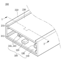
- FIG. 2 is a perspective view illustrating a lighting device including the light source module of FIG. 1, and FIG. 3 is a cross-sectional view of the lighting device cut along the line II ′ of FIG. 2.
- the lighting apparatus 200 of the first embodiment includes a light source module 100, a lower cover 210, and an upper cover 230.
- the light source module 100 may employ the technical features of the first embodiment of FIG. 1. Therefore, since the light source module 100 is the same as the first embodiment of FIG. 1, the same reference numerals will be used and detailed descriptions thereof will be omitted, and description will be given based on the features of the lower cover 210 and the upper cover 230. do.
- the lower cover 210 accommodates the light source module 100 and the upper cover 230.
- the lower cover 210 may be a metal material having excellent heat dissipation. That is, the lower cover 210 may be made of a material having high thermal conductivity.
- the lower cover 210 may include a first locking groove 211 in which the upper cover 230 is received in a horizontal direction corresponding to a length direction, and a second locking groove in which the light source module 100 is received in a horizontal direction. 213).
- the first locking groove 211 may be formed by first protrusions 212 protruding inward from the inner surface of the lower cover 210.
- the first protrusions 212 may extend in a lateral direction of the lower cover 210.
- the lower cover 210 and the upper cover 230 may be combined in a sliding type, but is not limited thereto. That is, the upper cover 230 may be inserted into the first locking groove 211 to be connected to the lower cover 210.
- the upper cover 230 includes a function of protecting the light source module 100 and diffusing the light emitted from the light source module 100.
- the second locking groove 213 may be formed by the second protrusion 214 spaced apart from the inner bottom surface of the lower cover 210 by a predetermined interval in an upward direction.
- the second protrusion 214 may protrude in an inner direction of the lower cover 210 and may extend in a lateral direction of the lower cover 210.
- the lower cover 210 and the light source module 100 may be coupled in a sliding type, but are not limited thereto. That is, the light source module 100 may have a substrate 110 inserted into the second locking groove 213 to be coupled to the lower cover 210.
- the lower surface of the substrate 110 may be in direct contact with the inner bottom surface of the lower cover 210, and heat from the light source module 100 may be conducted to the lower cover 210 having high thermal conductivity. have. Therefore, the lighting device 200 of the first embodiment has excellent advantages in heat dissipation as well as slimming and thinning.
- the lower surface of the substrate 110 is an insulating material. Direct contact with the lower cover 210 made of a conductive material having high thermal conductivity may prevent electrical deterioration such as shorting of the wiring pattern.
- a plurality of light emitting device packages 120, a plurality of driving devices 130, a wiring pattern 150, and first and second connection terminals 141 and 143 may be formed of a substrate (
- the light source module 100 located on one surface of all of the 110 is coupled to the inner bottom surface of the lower cover 210 in a sliding type, which is advantageous for slimming and thinning, and the lower surface of the substrate 110 is the lower cover ( Since it is in direct contact with the inner bottom surface of the 210 has excellent advantages in heat dissipation.
- FIG. 4 is a plan view illustrating an upper surface of the light source module according to the second embodiment
- FIG. 5 is a plan view illustrating the rear surface of the light source module according to the second embodiment.
- the light source module 100a according to the second embodiment may employ the technical features of the light source module of the first embodiment except for the plurality of driving devices 130a and the wiring pattern 150a. have. Therefore, the same configuration of the first and second embodiments denotes the same reference numerals, and detailed description thereof will be omitted.
- the substrate 110 may have a bar shape, a resin-based printed circuit board (PCB), a metal core PCB, a flexible PCB, a ceramic PCB, and a FR-4 substrate. It may include.
- the substrate 110 may include a printed circuit board having a metal layer therein.
- the substrate 110 includes one end 111 and the other end 112 positioned at both ends of the transverse direction Y.
- the substrate 110 may include one side 113 and the other side parallel to the horizontal direction Y of the substrate 110.
- the substrate 110 may include pads connected to the plurality of light emitting device packages 120, the plurality of driving devices 130a, and the connection terminal unit.
- the pads may be electrically connected to the wiring pattern 150a.
- Both side surfaces of the substrate 110 include first and second locking grooves 115 and 116.
- the first and second locking grooves 115 and 116 include a function for aligning and coupling the light source module 100a with the fixture of the lighting apparatus.
- the wiring pattern 150a may be formed on the rear surface 110b of the substrate 110.
- the wiring pattern 150a may include titanium (Ti), copper (Cu), nickel (Ni), gold (Au), chromium (Cr), tantalum (Ta), platinum (Pt), tin (Sn), and silver ( Ag), phosphorus (P) may be formed of at least one or an optional alloy thereof, and may be formed of a single layer or multiple layers.
- An insulating layer may be formed on the wiring pattern 150a.
- the substrate 110 may further include a contact hole connecting the wiring pattern 150a, the plurality of driving devices 130a, the plurality of light emitting device packages 120, and the connection terminal part. have.
- the plurality of light emitting device packages 120 may be mounted on the upper surface 110a of the substrate 110.
- the plurality of light emitting device packages 120 may be spaced apart from each other in a first direction corresponding to the horizontal direction Y of the substrate 110.
- the plurality of light emitting device packages 120 are limited to package type light emitting device packages 120, the present invention is not limited thereto, and a chip on which the chip is directly mounted on the top surface 110a of the substrate 110 may be used. board).
- the plurality of light emitting device packages 120 may be mounted at regular intervals in the horizontal direction Y of the substrate 110. That is, the plurality of light emitting device packages 120 may have a constant pitch (P) on the substrate 110. Since the plurality of light emitting device packages 120 have a constant pitch P on the substrate 110, uniform luminance in the lateral direction Y of the substrate 110 may be realized.
- the distance W1 between the light emitting device package 120 and both ends of the substrate 110 adjacent to both ends of the substrate 110 may be 1/2 of the pitch P between the plurality of light emitting device packages. have.
- the plurality of light emitting device packages 120 having a constant pitch are limited and described, but the present invention is not particularly limited.
- the plurality of light emitting device packages 120 may have different pitches for each region. For example, one end 111 or the other end 112 of the substrate 110 may have a narrow or wide pitch.
- the plurality of light emitting device packages 120 may have a narrower pitch toward the center of the substrate 110. In addition, the plurality of light emitting device packages 120 may have a narrower pitch as they are adjacent to both ends of the substrate 110.
- the plurality of driving elements 130a may be mounted on the upper surface 110a of the substrate 110 and may be disposed on one side surface 113 of the substrate 110 parallel to the lateral direction Y of the substrate 110. May be located adjacently.
- the plurality of driving devices 130a may be located between one side surface 113 of the substrate 110 and the plurality of light emitting device packages 120, but embodiments of the present disclosure are not limited thereto.
- the connection terminal unit may include a first connection terminal 141 adjacent to one end 111 of the substrate 110 and a second connection terminal 143 adjacent to the other end 112 of the substrate 110.
- the first and second connection terminals 141 and 143 may be mounted on the top surface 110a of the substrate 110 and may be parallel to the lateral direction Y of the substrate 110. It may be located adjacent to the side 113.
- the first and second connection terminals 141 and 143 may be located between the one side surface 113 of the substrate 110 and the plurality of light emitting device packages 120, but the embodiment is not limited thereto.
- the first and second connection terminals 141 and 143 may be located adjacent to the plurality of driving elements 130a.
- the first and second connection terminals 141 and 143 may be spaced apart from each other with the plurality of driving elements 130a interposed therebetween.
- the first and second connection terminals 141 and 143 may be located in parallel with the plurality of driving elements 130a.
- the first and second connection terminals 141 and 143 may be electrically connected to each other.
- the first and second connection terminals 141 and 143 may electrically connect the driving power source and the light source module 100a to receive the driving signal from an external driving power source, or may electrically connect the plurality of light source modules to each other. (connecter) function may be included.
- the first connection terminal 141 may be connected to an external driving power source
- the second connection terminal 143 may be connected to a connection terminal of another light source module.
- the first and second connection terminals 141 and 143 may be spaced apart from both ends of the substrate 110 by a predetermined interval.
- the gap W2 between the first and second connection terminals 141 and 143 and both ends of the substrate 110 is adjacent to both ends of the light emitting device package 120 and the substrate 110. It may be designed to be equal to or greater than the distance (W1) between both ends of the). That is, the first and second connection terminals 141 and 143 may have a distance or the same distance from both ends of the substrate 110 than the light emitting device package 120.
- the first and second connection terminals 141 and 143 may be mounted in a direction horizontal to the horizontal direction Y of the substrate 110, but is not limited thereto.
- the first and second connection terminals 141 and 143 may be mounted in the longitudinal direction X of the substrate 110, and are mounted in an inclined form between the transverse direction Y and the longitudinal direction X. May be
- the shape of the first and second connection terminals 141 and 143 may be changed according to a connection structure with an external driving power source and a coupling structure with another light source module.
- the first and second connection terminals 141 and 143 may be spaced apart from the plurality of light emitting device packages 120 by a predetermined interval.
- the distance between the first and second connection terminals 141 and 143 and the plurality of light emitting device packages 120 may be determined according to the full width at the half maximum (FWHM) of the light emitting device package 120. .
- the full width at half maximum (FWHM) of the light emitting device package 120 may be changed according to the directivity angle characteristic of the light emitting device package 120.
- an interval between the plurality of driving devices 130a and the plurality of light emitting device packages 120 may be determined according to the half width.
- the distance between the plurality of light emitting device packages 120 and the plurality of driving devices 130a may be changed according to the height of the plurality of driving devices 130a.
- a distance between the plurality of feet and the device package 120 and the first and second connection terminals 141 and 143 may be the plurality of driving elements 130a, the first and second connection terminals 141 and 143. It can be changed according to the height of.
- the full width at half maximum (FWHM) of the plurality of light emitting device packages 120 may be tan 10 ° to 30 °.
- the full width at half maximum (FWHM) of the plurality of light emitting device packages 120 is tan 30 ° (0.5774)
- the plurality of driving devices 130a and the first and second connection terminals 141 and 143 may vary according to height.
- a minimum distance from the plurality of light emitting device packages 120 may be determined, and the height and the distance may be inversely proportional to each other.
- the light source module 100a may include a plurality of driving devices 130a generating a driving voltage for driving the plurality of light emitting device packages 120 on the same substrate 110 as the light emitting device package 120. Mounting has the advantage of being slim and thin.
- the first and second connection terminals 141 and 143 may have a distance greater than or equal to the distance W1 between the plurality of light emitting device packages 120 and both ends of the substrate 110.
- the light source module 100a according to the second embodiment has an advantage in that the design design of the light emitting device package 120 is freer than that of a general light source module having connection terminals located at both ends of the substrate.
- FIG. 6 is a perspective view illustrating a lighting device including the light source module of FIG. 4, and FIG. 7 is a cross-sectional view of the lighting device cut along the line II-II ′ of FIG. 6.
- the lighting apparatus 200a may employ technical features of the light source module of the second embodiment except for the light source module 100a, the lower cover 210a, and the upper cover 230a. Therefore, since the light source module 100a is the same as the second embodiment of FIG. 4, the same reference numerals are used and detailed descriptions thereof will be omitted, and the lower cover 210a, the upper cover 230a, and the side cover 260 may be omitted. It will be described based on the features of the.
- the lower cover 210a accommodates the light source module 100a and the upper cover 230a.
- the lower cover 210a may be a metal material having excellent heat dissipation. That is, the lower cover 210a may be made of a material having high thermal conductivity.
- the lower cover 210a includes a structure in which an end of the side surface is bent so that the upper cover 230a may be seated, but is not limited thereto. That is, the lower cover 210a may include a structure in which the upper cover 230a is accommodated into protrusions protruding inwardly along an inner surface and a groove formed between the protrusions.
- the upper cover 230a may include a function of protecting the light source module 100a and diffusing light emitted from the light source module 100a.
- the side cover 260 covers both side ends of the light source module 100a.
- the size cover 260 is located on both ends of the lower cover 210a and is located below the upper cover 230a.
- the side cover 260 includes a function of fixing the light source module 100a and improving light extraction by reflecting light emitted from both ends of the light source module 100a.
- the side cover 260 includes a first hole 265.
- the first hole 265 may accommodate the fixing member 270 that couples the side cover 260, the light source module 100a, and the lower cover 210a to each other. That is, the first hole 265 may overlap the first and second coupling grooves 115 and 116 of the light source module 100a, and the second holes 265 may be formed on the bottom surfaces of both ends of the lower cover 210a. It may overlap with the hole 215.
- the fixing member 270 is fastened to the first hole 265, the first and second coupling grooves 115 and 116, and the second hole 215 so that the side cover 260, the light source module 100a, and And a function of engaging the lower cover 210a.
- the lighting apparatus 200a of the second embodiment will be described with a limited screw type, but is not limited thereto. That is, the fixing member 270 may be replaced with a coupling structure such as a hook type.
- An insulating member 220 is positioned between the light source module 100a and the lower cover 210a.
- the insulating member 220 may directly contact the rear surface of the light source module 100a and may directly contact the bottom surface of the lower cover 210a.
- the insulating member 220 may insulate between the wiring pattern 150a exposed on the rear surface of the light source module 100a and the bottom surface of the lower cover 210a.
- Heat from the light source module 100a may be conducted to the lower cover 210a having high thermal conductivity. Therefore, the lighting apparatus 200a of the second embodiment has excellent advantages in slimming and thinning as well as heat dissipation.
- the light source module 100a has a plurality of light emitting device packages 120 and a plurality of driving devices 130a positioned on an upper surface of the substrate 110, and thus the wiring pattern 150a exposed on the lower surface of the substrate 110.
- the silver insulating member 220 can prevent electrical deterioration such as short.
- a plurality of light emitting device packages 120, a plurality of driving devices 130a, and first and second connection terminals 141 and 143 may be disposed on an upper surface of the substrate 110.
- Both light source modules 100a are coupled to the inner bottom surface of the lower cover 210a with the insulating member 220 interposed therebetween, which is advantageous for slimming and thinning, and the lower surface of the substrate 110 is the lower cover ( Since the inner bottom surface of the 210a and the insulating member 220 are disposed to be adjacent to each other, the heat radiation may be excellent.
- FIG. 8 is a plan view illustrating a top surface of a light source module according to a third embodiment
- FIG. 9 is a plan view illustrating a rear surface of a light source module according to a third embodiment.
- the light source module 100b according to the third embodiment is the light source module of the first embodiment except for the plurality of driving elements 130b and the first and second wiring patterns 151b and 153b.
- the technical features of can be adopted. Accordingly, the same components in the first and third embodiments will be denoted by the same reference numerals, and detailed description thereof will be omitted. It includes.
- the substrate 110 may have a bar shape, a resin-based printed circuit board (PCB), a metal core PCB, a flexible PCB, a ceramic PCB, and a FR-4 substrate. It may include.
- the substrate 110 may include a printed circuit board having a metal layer therein.
- the substrate 110 includes one end 111 and the other end 112 positioned at both ends of the transverse direction Y.
- the substrate 110 includes one side 113 and the other side 114 parallel to the lateral direction Y of the substrate 110.
- the substrate 110 may include pads connected to the plurality of light emitting device packages 120, the plurality of driving devices 130b, and the connection terminal unit.
- the pads may be electrically connected to the first and second wiring patterns 151b and 153b.
- the plurality of light emitting device packages 120 may be mounted on the upper surface 110a of the substrate 110.
- the plurality of light emitting device packages 120 may be spaced apart from each other in a first direction corresponding to the horizontal direction Y of the substrate 110.
- the plurality of light emitting device packages 120 are limited to package type light emitting device packages 120, the present invention is not limited thereto, and a chip on which the chip is directly mounted on the top surface 110a of the substrate 110 may be used. board).
- the plurality of light emitting device packages 120 may be mounted at regular intervals in the horizontal direction Y of the substrate 110. That is, the plurality of light emitting device packages 120 may have a constant pitch (P) on the substrate 110. Since the plurality of light emitting device packages 120 have a constant pitch P on the substrate 110, uniform luminance in the lateral direction Y of the substrate 110 may be realized.
- the distance W1 between the light emitting device package 120 and both ends of the substrate 110 adjacent to both ends of the substrate 110 may be 1/2 of the pitch P between the plurality of light emitting device packages. have.
- a plurality of light emitting device packages 120 having a constant pitch are limited and described, but the present invention is not particularly limited.
- the plurality of light emitting device packages 120 may have different pitches for each region. For example, one end 111 or the other end 112 of the substrate 110 may have a narrow or wide pitch.
- the plurality of light emitting device packages 120 may have a narrower pitch toward the center of the substrate 110. In addition, the plurality of light emitting device packages 120 may have a narrower pitch as they are adjacent to both ends of the substrate 110.
- the first wiring pattern 151b may be formed on the top surface 110a of the substrate 110.
- the first wiring pattern 151b includes titanium (Ti), copper (Cu), nickel (Ni), gold (Au), chromium (Cr), tantalum (Ta), platinum (Pt), tin (Sn), It may be formed of at least one of silver (Ag), phosphorus (P) or an optional alloy thereof, and may be formed of a single layer or multiple layers.
- An insulating layer may be formed on the first wiring pattern 151b.
- the plurality of driving elements 130b may be mounted on the rear surface 110b of the substrate 110, and may have one side surface 113 of the substrate 110 parallel to the lateral direction Y of the substrate 110, or It may be located adjacent to the other side 114 or overlapping with the plurality of light emitting device package 120, but is not limited thereto.
- the second wiring pattern 153b may be formed on the rear surface 110b of the substrate 110.
- the second wiring pattern 153b includes titanium (Ti), copper (Cu), nickel (Ni), gold (Au), chromium (Cr), tantalum (Ta), platinum (Pt), tin (Sn), It may be formed of at least one of silver (Ag), phosphorus (P) or an optional alloy thereof, and may be formed of a single layer or multiple layers.
- An insulating layer may be formed on the second wiring pattern 153b.
- the first and second wiring patterns 151b and 153b are electrically connected to the substrate 110 to connect the plurality of driving devices 130b, the plurality of light emitting device packages 120, and a connection terminal to each other. It further includes one or more contact holes 150b.
- the connection terminal unit may include a first connection terminal 141 adjacent to one end 111 of the substrate 110 and a second connection terminal 143 adjacent to the other end 112 of the substrate 110.
- the first and second connection terminals 141 and 143 may be mounted on the rear surface 110b of the substrate 110, and the substrate 110 may be parallel to the lateral direction Y of the substrate 110. It may be located adjacent to one side 113 of the, and may be located in parallel with the plurality of driving elements (130b).
- connection terminal portion may be variously changed.
- the connection terminal portion may be positioned on the upper surface 110a of the substrate 110, and may be spaced apart from the plurality of driving elements 130b in the longitudinal direction X.
- the first and second connection terminals 141 and 143 of the third embodiment may be adjacent to the plurality of driving elements 130b.
- the first and second connection terminals 141 and 143 may be spaced apart from each other with the plurality of driving elements 130b interposed therebetween.
- the first and second connection terminals 141 and 143 may be located in parallel with the plurality of driving elements 130b.
- the first and second connection terminals 141 and 143 may be electrically connected to each other.
- the first and second connection terminals 141 and 143 may be electrically connected to the driving power source and the light source module 100b in order to receive a driving signal from an external driving power source, or to electrically connect the plurality of light source modules to each other. (connecter) function may be included.
- the first connection terminal 141 may be connected to an external driving power source
- the second connection terminal 143 may be connected to a connection terminal of another light source module.
- the first and second connection terminals 141 and 143 may be spaced apart from both ends of the substrate 110 by a predetermined interval.
- the gap W2 between the first and second connection terminals 141 and 143 and both ends of the substrate 110 is adjacent to both ends of the light emitting device package 120 and the substrate 110. It may be designed to be equal to or greater than the distance (W1) between both ends of the). That is, the first and second connection terminals 141 and 143 may have a distance or the same distance from both ends of the substrate 110 than the light emitting device package 120.
- the first and second connection terminals 141 and 143 may be mounted in a direction horizontal to the horizontal direction Y of the substrate 110, but is not limited thereto.
- the first and second connection terminals 141 and 143 may be mounted in the longitudinal direction X of the substrate 110, and are mounted in an inclined form between the transverse direction Y and the longitudinal direction X. May be
- the shape of the first and second connection terminals 141 and 143 may be changed according to a connection structure with an external driving power source and a coupling structure with another light source module.
- a plurality of light emitting device packages 120 are positioned on the top surface 110a of the substrate 110, and a plurality of driving devices are disposed on the back surface 110b of the substrate 110. 130b and first and second connection terminals 141 and 143 may be located. Accordingly, the light source module 100b according to the third embodiment may include the plurality of driving devices 130b that generate driving voltages for driving the plurality of light emitting device packages 120, and the same substrate 110 as the light emitting device package 120. ) Is advantageous in slimming and thinning.
- the first and second connection terminals 141 and 143 according to the third embodiment are spaced apart from or equal to the distance W1 between the plurality of light emitting device packages 120 and both ends of the substrate 110.
- the light source module 100b according to the third exemplary embodiment has an advantage in that the design design of the light emitting device package 120 is freer than that of a general light source module having connection terminals located at both ends of the substrate.
- FIG. 10 is a cross-sectional view of a lighting device including the light source module of FIG. 8.
- the lighting apparatus 200b includes a light source module, a body portion 210b, an upper cover 230b, and first and second optical lenses 221 and 223.
- the light source module may employ the technical features of the third embodiment of FIG. 8. Therefore, since the light source module is the same as the third embodiment of FIG. 8, the same reference numerals are used and detailed descriptions thereof will be omitted, and the body portion 210b, the upper cover 230b, and the first and second optical lenses may be omitted. 221, 223 will be described based on the features.
- the body part 210b accommodates the light source module, the first optical lens 221, the second optical lens 223, and the upper cover 230b.
- the body portion 210b may include a metal material having excellent heat dissipation. That is, the body portion 210b may be made of a material having high thermal conductivity.
- the body portion 210b may have a structure in which an upper surface is opened, and may include a stepped structure along an edge of the upper surface so that the upper cover 230b may be seated, but is not limited thereto. That is, the body portion 210b may be formed with a groove along the inner side of the upper surface.
- the body portion 210b may include at least one protrusion along the inner surface. The groove formed by the one or more protrusions formed on the inner surface may accommodate the first and second optical lenses 221 and 223.
- the upper cover 230b includes a function of protecting the light source module, the first and second optical lenses 221 and 223, and diffusing the light emitted from the light source module.
- the first and second optical lenses 221 and 223 may include a function of diffusing, condensing or converting light from the light source module.
- the illumination device 200b of the third embodiment has been described in a limited configuration of the first and second optical lenses 221 and 223, the number and location may be changed.
- the lighting apparatus 200b of the third embodiment may include a fixing member for coupling the body portion 210b, the light source module, the upper cover 230b, and the first and second optical lenses 221 and 223 to each other.
- the fixing member may be a screw type, a hook type, or the like, but is not limited thereto.
- the lighting apparatus 200b of the third embodiment may directly conduct heat from the light source module to the body portion 210b having high thermal conductivity. Therefore, the lighting apparatus 200b of the third embodiment has an excellent advantage in heat dissipation as well as slimming and thinning.
- the light source module includes a plurality of light emitting device packages 120 disposed on the top surface 110a of the substrate 110, and a plurality of driving devices 130b, first and second connections to the back surface 110b of the substrate 110. Since the terminals 141 and 143 are located, the design design of the components mounted on the substrate 110 is free.
- 11 to 13 are plan views illustrating lighting apparatuses in which a plurality of light source modules are coupled.
- the lighting apparatus 300 of the fourth embodiment includes first and second light source modules 100c and 100d.
- the first and second light source modules 100c and 100d may adopt technical features of the first to third embodiments of FIGS. 1, 4, 5, 8, and 9.
- the first light source module 100c includes a plurality of first light emitting device packages 120a, first and second connection terminals 141a and 143a, and the second light source module 100d includes a plurality of second light emitting devices.
- the device package 120b includes third and fourth connection terminals 141b and 143b.
- the first connection terminal 141a may be connected to each other by the fourth connection terminal 143b and a connection member.
- the connection member may be a wire (W), but is not limited thereto.
- first and second light source modules 100c and 100d are disposed in the horizontal direction, and the first and fourth connection terminals 141a and 143b are electrically connected to each other to provide one lighting device 300. .
- the first and second light emitting device packages 120a and 120b may have a constant pitch.
- the first and second plurality of light emitting device packages 120a and 120b have a constant pitch in the transverse direction of the first and second light source modules 100c and 100d, thereby providing the first and second light source modules ( Uniform luminance can be realized in the transverse direction of 100c and 100d).
- first and second light emitting device packages 120a and 120b having a constant pitch
- present invention is not limited thereto.
- the first and second plurality of light emitting device packages 120a and 120b may have different pitches depending on regions.
- the fifth lighting device 400 includes first and second light source modules 100c and 100d.
- the first and second light source modules 100c and 100d may employ technical features of the first to third embodiments of FIGS. 1, 4, 5, 8, and 9.
- the first light source module 100c includes a plurality of first light emitting device packages 120a and first and second connection terminals 141a and 141b, and the second light source module 100d includes a plurality of second light emitting devices.
- the device package 120b includes third and fourth connection terminals 141b and 143b.
- the first connection terminal 141a may be connected to each other by the fourth connection terminal 143b and the wire (W).
- first and second light source modules 100c 100d are disposed in the longitudinal direction, and the first and fourth connection terminals 141a and 143b are electrically connected to each other to provide one lighting device 400.
- the first and second light emitting device packages 120a and 120b may have a constant pitch.
- the first and second plurality of light emitting device packages 120a and 120b may have constant pitches in the transverse and longitudinal directions of the first and second light source modules 100a and 100b. Therefore, the lighting device 400 may implement uniform luminance in the entire area.
- first and second light emitting device packages 120a and 120b having a constant pitch
- present invention is not limited thereto.
- the first and second plurality of light emitting device packages 120a and 120b may have different pitches depending on regions.
- the sixth lighting device 500 includes first to eighth light source modules 100c to 100j.
- the first to eighth light source modules 100c to 100j may employ technical features of the first to third embodiments of FIGS. 1, 4, 5, 8, and 9.
- the first light source module 100c includes a plurality of first light emitting device packages 120a, first and second connection terminals 141a and 143a, and the second light source module 100d includes a plurality of second light emitting devices.
- the device package 120b includes third and fourth connection terminals 141b and 143b.
- the third light source module 100e includes a plurality of third light emitting device packages 120c and fifth and sixth connection terminals 141c and 143c
- the fourth light source module 100f includes a plurality of fourth light emitting devices.
- the device package 120d and the seventh and eighth connection terminals 141d and 143d are included.
- the fifth light source module 100g includes a plurality of fifth light emitting device packages 120e, ninth and tenth connection terminals 141e and 143e, and the sixth light source module 100hf includes a plurality of sixth light emitting elements.
- the device package 120f includes eleventh and twelfth connection terminals 141f and 143f.
- the seventh light source module 100i includes a plurality of seventh light emitting device packages 120g, thirteenth and fourteenth connection terminals 141g and 143g, and the eighth light source module 100j includes a plurality of eighth light emission.
- the device package 120h and the fifteenth and sixteenth connection terminals 141h and 143h are included.
- the first connection terminal 141a may be connected to each other by the fourth connection terminal 143b and the wire (W).
- the third connection terminal 141b may be connected to the sixth connection terminal 143b.
- the fifth connection terminal 141c may be connected to the eighth connection terminal 143d.
- the seventh connection terminal 141d may be connected to the tenth connection terminal 143e.
- the ninth connection terminal 141e may be connected to the twelfth connection terminal 143f.
- the eleventh connection terminal 141f may be connected to the fourteenth connection terminal 143g.
- the thirteenth connection terminal 141g may be connected to the sixteenth connection terminal 143h.
- the first to eighth light source modules 100c to 100j are electrically connected to the first, third to fourteenth, and sixteenth connection terminals 141a, 141b to 143g, and 143h in the longitudinal direction and the transverse direction.
- One lighting device 500 is provided.
- the fourth light source module 100f and the sixth light source module 100h include seventh, eighth, eleventh, and twelfth connection terminals 141d, 143d, 141f, and 143f positioned in symmetrical directions.
- the lighting device 500 according to the embodiment has positions of the seventh, eighth, eleventh, and twelfth connection terminals 141d, 143d, 141f, and 143f according to the positions where the first to eighth light source modules 100c to 100j are coupled. Can be changed.
- the first to eighth light emitting device packages 120a to 120h may have a constant pitch.
- the first to eighth light emitting device packages 120a to 120h may have constant pitches in the transverse and longitudinal directions of the first and second light source modules 100c to 100j. Therefore, the lighting device 500 has an advantage of providing uniform surface light of a large screen such as a large screen display device.
- first to eighth light emitting device packages 120a to 120h having a constant pitch are described, but the embodiment is not limited thereto.
- the first to eighth light emitting device packages 120a to 120h may have different pitches for respective regions according to a purpose.
- the lighting apparatuses 300, 400, and 500 according to FIGS. 11 to 13 have an advantage of providing various types of surface light using at least one light source module.
- FIG. 14 is a view illustrating a driving circuit of a light source module according to an embodiment.
- FIG. 14 is a view illustrating a driving circuit of a light source module according to an embodiment.
- the driving circuit 600 of the light source module includes an AC power source (V AC ), a rectifier 610, a driving module 620, and first and second light emitting groups 630 and 640. Include.
- the first and second light emitting groups 630 and 640 may be light source modules including a plurality of light emitting device packages. That is, the first and second light emitting groups 630 and 640 may adopt technical features of the light source module of FIG. 1.
- the driving circuit 600 of the light source module has described the first and second light emitting groups 630 and 640 as an example, but is not limited thereto. Therefore, the light emitting group may be at least three or more.
- the first and second light emitting groups 630 and 640 may have different forward voltage levels, respectively. For example, when the first and second light emitting groups 630 and 640 respectively include different numbers of light emitting device packages, they may have different forward voltage levels.
- the rectifier 610 rectifies the AC voltage from the AC power supply V AC to generate a driving voltage, and outputs the generated driving voltage.
- the rectifier 610 is not particularly limited, and any one of various known rectifier circuits, such as a full-wave rectifier circuit and a half-wave rectifier circuit, may be used.
- the rectifier 610 may be a bridge full-wave rectifier circuit composed of four diodes.
- the driving module 620 controls the first and second light emitting groups 630 and 640 using the driving voltage.
- the driving module 620 may sequentially drive the first and second light emitting groups 630 and 640 for a plurality of sections.
- the driving module 620 may sequentially drive the first and second light emitting groups 630 and 640 during the first and second periods of sequentially driving the first and second light emitting groups 630 and 640. Can be.
- the first section may be defined as a section in which the voltage level of the driving voltage input from the rectifier 610 is supplied with a driving voltage between the first forward voltage level and the second forward voltage level.
- the second forward voltage level is greater than the first forward voltage level.
- the driving module 620 controls the first light emitting group 630 to be driven during the first period.
- the second section may be defined as a section in which the voltage level of the driving voltage input from the rectifier 610 is supplied with a driving voltage between the second forward voltage level and the third forward voltage level.
- the third forward voltage level is greater than the second forward voltage level.
- the driving module 620 controls the first and first light emitting groups 630 and 640 to be driven during the second period.
- the driving circuit 600 of the light source module of the embodiment includes the flicker compensator 650.
- the flicker compensator 650 includes a function for improving flicker that occurs during sequential driving.
- the flicker compensator 650 includes, but is not limited to, a capacitor C and first and second resistors R1 and R2.
- the flicker compensator 650 may be connected in parallel with the first and second light emitting groups 630 and 640.
- the flicker compensator 650 may be charged at or above the first forward voltage level, and may be discharged at or below the first forward voltage level.
- a section in which a driving voltage below the first forward voltage level is supplied is defined as a third section.
- the driving circuit 600 of the light source module according to the embodiment may drive the first and second light emitting groups 630 and 640 using the charge charged in the capacitor C in a section below the first forward voltage level.
- the flicker compensator 650 may drive the first and second light emitting groups 630 and 640 to remove flickers of the light source module during the third period to improve flicker.
- 15 is a cross-sectional view illustrating a light emitting device package included in a light source module according to an embodiment.
- the light emitting device package 700 may include a body 750, a first lead electrode 721 and a second lead electrode 723 disposed at least partially on the body 750, and the body ( The light emitting device 800 electrically connected to the first lead electrode 721 and the second lead electrode 723 on the 750, and a molding surrounding the light emitting device 800 on the body 750. And a member 730.
- the body 750 may be formed including a silicon material, a synthetic resin material, or a metal material.
- the first lead electrode 721 and the second lead electrode 723 are electrically separated from each other, and may be formed to penetrate the inside of the body 750. That is, some of the first lead electrode 721 and the second lead electrode 723 may be disposed inside the cavity, and the other part may be disposed outside the body 750.
- the first lead electrode 721 and the second lead electrode 723 may supply power to the light emitting device 800 and may reflect light generated by the light emitting device 800 to increase light efficiency. It may also function to discharge heat generated from the light emitting device 800 to the outside.
- the light emitting device package 700 may be applied to a light unit.
- the light unit includes a structure in which a plurality of light emitting devices or light emitting device packages are arranged, and may include a lighting lamp, a traffic light, a vehicle headlight, an electronic sign board, and the like.
- 16 and 17 are cross-sectional views illustrating an embodiment of a light emitting device included in the light emitting device package of FIG. 15.
- the light emitting device 801 has a horizontal type, and includes a substrate 11, a buffer layer 13, a light emitting structure 20, an electrode layer 30, a first electrode pad 51, and a second electrode. Pad 53 and current blocking layer 40.
- a light-transmissive may be used an insulating or conductive substrate such as sapphire (Al 2 O 3), SiC, Si, GaAs, GaN, ZnO, Si, GaP, InP, Ge, Ga 2 O 3 , LiGaO 3 , or quartz can be used.
- a plurality of protrusions may be formed on an upper surface of the substrate 11, and the plurality of protrusions may be formed by etching the substrate 11 or may be formed of a light extraction structure such as a separate roughness. Can be.
- the protrusion may include a stripe shape, a hemispherical shape, or a dome shape.
- the buffer layer 13 may be formed on the substrate 11 and may be formed to mitigate the difference in lattice constant between the substrate 11 and the nitride-based semiconductor layer, and may function as a defect control layer. .
- the buffer layer 13 may have a value between lattice constants between the substrate 11 and the nitride-based semiconductor layer.
- the buffer layer 13 may be formed of an oxide such as a ZnO layer, but is not limited thereto.
- the light emitting structure 20 is positioned on the substrate 11.
- the light emitting structure 20 includes a first conductive semiconductor layer 21, an active layer 22, and a second conductive semiconductor layer 23.
- the first conductivity type semiconductor layer 21 may be formed of a single layer or multiple layers.
- the first conductive semiconductor layer 21 may be a group III-V compound semiconductor doped with a first conductive dopant.
- the first conductivity type dopant may be an n-type dopant and may include Si, Ge, Sn, Se, or Te, but is not limited thereto.
- the first conductivity type semiconductor layer 21 may include a semiconductor material having a composition formula of In x Al y Ga 1-xy N (0 ⁇ x ⁇ 1, 0 ⁇ y ⁇ 1, 0 ⁇ x + y ⁇ 1). Can be.
- the first conductive semiconductor layer 21 may be formed of any one or more of GaN, InN, AlN, InGaN, AlGaN, InAlGaN, AlInN, AlGaAs, InGaAs, AlInGaAs, GaP, AlGaP, InGaP, AlInGaP, InP.
- the active layer 22 may be any one of a single quantum well structure, a multi quantum well structure (MQW), a quantum-wire structure, or a quantum dot structure.
- the active layer 22 may include a well layer and a barrier layer formed of a gallium nitride based semiconductor layer.
- the active layer 22 may be at least one pair of InGaN / GaN, InGaN / InGaN, GaN / AlGaN, InAlGaN / GaN, GaAs / AlGaAs, InGaAs / AlGaAs, GaInP / AlGaInP, GaP / AlGaP, InGaP / AlGaP. It may be formed as a structure, but is not limited thereto.
- the well layer may be formed of a material having a lower band gap than the band gap of the barrier layer.
- the barrier layer and the well layer of the active layer 22 may be formed as an undoped layer which is not doped with impurities to improve crystal quality of the active layer, but impurities may be doped in some or all active regions to lower the forward voltage. have.
- the second conductivity type semiconductor layer 23 may be disposed on the active layer 22 and be formed of a single layer or multiple layers.
- the second conductive semiconductor layer 23 may be a group III-V compound semiconductor doped with a second conductive dopant.
- the second conductivity type dopant may be a p type dopant, and may include Mg, Zn, Ca, Sr, Ba, and the like, but is not limited thereto.
- the second conductive semiconductor layer 23 may be formed of any one of compound semiconductors such as GaN, AlN, AlGaN, InGaN, InN, InAlGaN, AlInN, AlGaAs, GaP, GaAs, GaAsP, AlGaInP, GaP.
- the first electrode pad 51 is positioned on the first conductive semiconductor layer 21.
- the second electrode pad 53 is positioned on the second conductive semiconductor layer 23.
- the first electrode pad 51 and the second electrode pad 53 are Ti, Ru, Rh, Ir, Mg, Zn, Al, In, Ta, Pd, Co, Ni, Si, Ge, Ag, Au and Au It can be selected from an optional alloy of.
- the electrode layer 30 is a current diffusion layer and may be formed of a material having transparency and electrical conductivity.
- the electrode layer 30 may be formed to have a refractive index lower than that of the compound semiconductor layer.
- the electrode layer 30 may be formed on the second conductive semiconductor layer 23 to be in ohmic contact with the second conductive semiconductor layer 23.
- the electrode layer 30 may be a transparent conductive oxide or a transparent metal layer.
- the electrode layer 30 may include indium tin oxide (ITO), indium zinc oxide (IZO), indium zinc tin oxide (IZTO), indium aluminum zinc oxide (IAZO), indium gallium zinc oxide (IGZO), and indium gallium tin (IGTO). oxide), aluminum zinc oxide (AZO), antimony tin oxide (ATO), gallium zinc oxide (GZO), ZnO, IrOx, RuOx, NiO, and the like, and may be formed in at least one layer.
- ITO indium tin oxide
- IZO indium zinc oxide
- the current blocking layer 40 overlaps with the second electrode pad 53 and has a function of preventing current from being concentrated in the lower portion of the second electrode pad 53.
- the current blocking layer 40 may be formed of an insulating material such as oxide or nitride.
- the current blocking layer 40 may be formed by selecting at least one selected from the group consisting of Si x O y , Si x N y , SiO x N y , Al 2 O 3 , TiO 2 , AlN, and the like. It is not limited to this.
- the current blocking layer 40 may include a distributed Bragg reflector (DBR) in which layers having different refractive indices are alternately stacked, but is not limited thereto.
- DBR distributed Bragg reflector
- a light emitting device 802 may be formed in a vertical type with a light emitting structure 20, a first electrode pad 51 disposed on the light emitting structure 20, and under the light emitting structure 20.
- a second electrode pad 53 positioned between the light emitting structure 20 and the second electrode pad 53, a current blocking layer 40 vertically corresponding to the first electrode pad 51, and a supporting member (60).
- the light emitting structure 20 is positioned on the substrate 11.
- the light emitting structure 20 includes a first conductive semiconductor layer 21, an active layer 22, and a second conductive semiconductor layer 23.
- the second electrode pad 53 may include a contact layer 55, a reflective layer 56, and a bonding layer 57 positioned under the second conductive semiconductor layer 23 of the light emitting structure 20. .
- the contact layer 55 may be in contact with the bottom surface of the second conductivity type semiconductor layer 23, and part of the contact layer 55 may extend to the bottom surface of the current blocking layer 40.
- the contact layer 55 may be a conductive material such as ITO, IZO, IZTO, IAZO, IGZO, IGTO, AZO, ATO, or a metal of Ni and Ag.
- a reflective layer 56 may be formed below the contact layer 55, and the reflective layer 56 may be formed of Ag, Ni, Al, Rh, Pd, Ir, Ru, Mg, Zn, Pt, Au, Hf, or a combination thereof. It may be formed of a structure including at least one layer made of a material selected from the group consisting of.
- the reflective layer 56 may be contacted under the second conductive semiconductor layer 23, and may be in ohmic contact with a metal or ohmic contact with a conductive material such as ITO, but is not limited thereto.
- a bonding layer 57 may be formed below the reflective layer 56, and the bonding layer 57 may be used as a barrier metal or a bonding metal, and the material may be, for example, Ti, Au, Sn, Ni, It may comprise at least one of Cr, Ga, In, Bi, Cu, Ag and Ta and an optional alloy.
- the channel layer 70 may be disposed under the light emitting structure 20.
- the channel layer 70 may be formed along an edge of the lower surface of the second conductive semiconductor layer 23 and may be formed in a ring shape, a loop shape, or a frame shape.
- the channel layer 70 may include at least one of ITO, IZO, IZTO, IAZO, IGZO, IGTO, AZO, ATO, SiO 2 , SiO x , SiO x N y , Si 3 N 4 , Al 2 O 3 , and TiO 2 . It may include.
- An inner part of the channel layer 70 may be disposed under the second conductive semiconductor layer 23, and an outer part of the channel layer 70 may be located outside the side of the light emitting structure 20.
- a support member 60 may be formed below the bonding layer 57, and the support member 60 may be formed of a conductive member, and the material may be copper (copper), gold (au), or nickel. (Ni-nickel), molybdenum (Mo), copper-tungsten (Cu-W), and a carrier wafer (eg, Si, Ge, GaAs, ZnO, SiC, etc.).
- a carrier wafer eg, Si, Ge, GaAs, ZnO, SiC, etc.
- the support member 60 may be implemented as a conductive sheet.
- the second electrode pad 53 may include the support member 60. At least one or a plurality of layers of the second electrode pad 53 may have the same width as the support member 60. Can be.
- a light extraction structure such as roughness may be formed on an upper surface of the first conductive semiconductor layer 21.
- the first electrode pad 51 may be disposed on a flat surface of the upper surface of the first conductive semiconductor layer 21, but is not limited thereto.
- An insulating layer (not shown) may be further formed on side and top surfaces of the light emitting structure 20, but embodiments are not limited thereto.
- the current blocking layer 40 overlaps with the first electrode pad 51 and has a function of preventing current from being concentrated in the lower portion of the second electrode pad 53.
- the current blocking layer 40 may be formed of an insulating material such as oxide or nitride.
- the current blocking layer 40 may be formed by selecting at least one selected from the group consisting of Si x O y , Si x N y , SiO x N y , Al 2 O 3 , TiO 2 , AlN, and the like. It is not limited to this.
- the current blocking layer 40 may include a distributed Bragg reflector (DBR) in which layers having different refractive indices are alternately stacked, but is not limited thereto.
- DBR distributed Bragg reflector
- the light emitting devices 801 and 802 are described with respect to the horizontal and vertical types, the present invention is not limited thereto, and the light emitting devices 801 and 802 may include a flip type in which an electrode pad is disposed only below.
Abstract
Description
Claims (20)
- 기판;상기 기판의 상에 위치한 복수의 발광 소자 패키지;상기 기판의 상에 위치한 복수의 구동소자; 및상기 기판의 상에 위치한 연결 단자부를 포함하고,상기 기판의 양끝단과 상기 연결 단자부 사이의 간격은 상기 기판의 양끝단과 인접한 상기 발광 소자 패키지와 상기 기판의 양끝단 사이의 간격 이상인 광원 모듈.
- 제1 항에 있어서,상기 복수의 발광 소자 패키지, 복수의 구동소자 및 연결단자부는 상기 기판의 상면 상에 배치된 광원 모듈.
- 제1 항에 있어서,상기 기판의 상면상에는 상기 복수의 구동소자, 상기 복수의 발광 소자 패키지, 및 상기 연결 단자부를 전기적으로 연결하는 배선 패턴을 더 포함하는 광원 모듈.
- 제1 항에 있어서,상기 연결 단자부는 상기 기판의 일단과 인접한 제1 연결 단자와, 상기 기판의 타단과 인접한 제2 연결 단자를 포함하는 광원 모듈.
- 제1 항에 있어서,상기 기판의 양끝단과 인접한 상기 발광 소자 패키지와 상기 기판의 양끝단 사이의 간격은 상기 복수의 발광 소자 패키지 사이의 피치의 1/2의 길이를 갖는 광원 모듈.
- 제1 항에 있어서,상기 기판의 배면에 배치된 배선패턴을 더 포함하는 광원 모듈.
- 제6 항에 있어서,상기 기판에는 상기 배선 패턴, 상기 복수의 발광 소자 패키지, 상기 복수의 구동소자, 및 상기 연결 단자부를 전기적으로 연결하는 컨택홀을 더 포함하는 광원 모듈.
- 제1 항에 있어서,상기 복수의 발광 소자 패키지 및 연결단자부는 상기 기판의 일면 상에 배치되고, 상기 복수의 구동소자는 상기 기판의 배면에 배치된 광원 모듈.
- 제8 항에 있어서,상기 기판의 상면에 상기 복수의 발광 소자 패키지와 연결된 제1 배선 패턴;상기 기판의 하면에 상기 복수의 구동소자와 연결된 제2 배선 패턴; 및상기 제1 및 제2 배선 패턴을 전기적으로 연결하는 컨택홀을 더 포함하는 광원 모듈.
- 제1 항에 있어서,상기 연결 단자부는 상기 기판의 일단과 인접한 제1 연결 단자와, 상기 기판의 타단과 인접한 제2 연결 단자를 포함하는 광원 모듈.
- 제10 항에 있어서,상기 제1 및 제2 연결 단자는 상기 기판의 횡방향과 평행한 방향으로 실장된 광원 모듈.
- 제7 항에 있어서,상기 제1 및 제2 연결 단자는 상기 기판의 종방향과 평행한 방향으로 실장된 광원 모듈.
- 제7 항에 있어서,상기 제1 및 제2 연결 단자는 상기 기판의 횡방향 및 종방향 사이의 방향으로 기울어지게 실장된 광원 모듈.
- 제1 항 내지 제13 항 중 어느 하나의 광원모듈을 포함하는 조명 장치.
- 제14 항에 있어서,상기 광원 모듈을 수납하는 하부 커버와, 상기 하부 커버를 덮는 상부 커버를 포함하고,상기 하부 커버는,내측면으로부터 내측방향으로 돌출된 제1 돌기들;상기 제1 돌기들에 의해 형성되어 상기 상부 커버가 슬라이딩 타입으로 결합되는 제1 걸림홈;상기 하부 커버는 내부 바닥면으로부터 일정 간격 이격되어 내측면으로부터 내측방향으로 돌출된 제2 돌기; 및상기 바닥면과 상기 제2 돌기 사이에 형성되어 상기 광원 모듈이 슬라이딩 타입으로 결합되는 제2 걸림홈을 포함하고,상기 기판의 하부면은 상기 하부 커버의 바닥면과 직접 접촉되는 조명 장치.
- 제14 항에 있어서,상기 광원 모듈과 상기 하부 커버 사이에는 절연부재; 및상기 하부 커버의 양측단에 상기 광원 모듈의 양측단을 덮는 사이드 커버를 포함하고,상기 사이드 커버는 고정부재가 삽입되는 제1 홀을 포함하고, 상기 하부 커버의 바닥면에는 상기 제1 홀과 대응되는 제2 홀을 포함하고, 상기 광원 모듈의 제1 및 제2 걸림홈 각각은 상기 제1 및 제2 홀과 중첩된 조명 장치.
- 제14 항에 있어서,상기 광원 모듈을 수납하는 상면이 개구된 바디부;상기 바디부의 상면을 덮는 상부 커버; 및상기 광원 모듈 상에 위치한 적어도 하나 이상의 광학 렌즈를 포함하는 조명 장치.
- 제1 항 내지 제13 항 중 어느 하나에 기재된 제1 광원 모듈;제1 항 내지 제13 항 중 어느 하나에 기재된 제2 광원 모듈; 및상기 제1 광원 모듈과 상기 제2 광원 모듈을 연결하는 연결부재를 포함하는 조명 장치.
- 제18 항에 있어서,상기 제1 및 제2 광원 모듈을 횡방향 또는 종방향으로 연결되는 조명 장치.
- 청구항 18에 있어서,상기 제1 광원 모듈은 복수개로 이루어지고,상기 제2 광원 모듈은 복수개로 이루어지고,상기 제1 및 제2 광원 모듈은 횡방향 및 종방향으로 서로 연결되는 조명 장치.
Priority Applications (2)
| Application Number | Priority Date | Filing Date | Title |
|---|---|---|---|
| US15/544,436 US10627088B2 (en) | 2015-01-19 | 2016-01-19 | Light source module and lighting device |
| JP2017537959A JP6710215B2 (ja) | 2015-01-19 | 2016-01-19 | 光源モジュール及び照明装置{light source module and lighting device} |
Applications Claiming Priority (6)
| Application Number | Priority Date | Filing Date | Title |
|---|---|---|---|
| KR1020150008707A KR20160089142A (ko) | 2015-01-19 | 2015-01-19 | 광원 모듈 및 조명 장치 |
| KR10-2015-0008707 | 2015-01-19 | ||
| KR10-2015-0010571 | 2015-01-22 | ||
| KR1020150010571A KR20160090590A (ko) | 2015-01-22 | 2015-01-22 | 광원 모듈 및 조명 장치 |
| KR10-2015-0049710 | 2015-04-08 | ||
| KR1020150049710A KR20160120527A (ko) | 2015-04-08 | 2015-04-08 | 광원 모듈 및 조명 장치 |
Publications (1)
| Publication Number | Publication Date |
|---|---|
| WO2016117905A1 true WO2016117905A1 (ko) | 2016-07-28 |
Family
ID=56417370
Family Applications (1)
| Application Number | Title | Priority Date | Filing Date |
|---|---|---|---|
| PCT/KR2016/000548 WO2016117905A1 (ko) | 2015-01-19 | 2016-01-19 | 광원 모듈 및 조명 장치 |
Country Status (3)
| Country | Link |
|---|---|
| US (1) | US10627088B2 (ko) |
| JP (1) | JP6710215B2 (ko) |
| WO (1) | WO2016117905A1 (ko) |
Cited By (4)
| Publication number | Priority date | Publication date | Assignee | Title |
|---|---|---|---|---|
| JP2018085212A (ja) * | 2016-11-22 | 2018-05-31 | パナソニックIpマネジメント株式会社 | 照明装置 |
| JP2018098126A (ja) * | 2016-12-16 | 2018-06-21 | パナソニックIpマネジメント株式会社 | 発光装置及び照明装置 |
| JP2018125265A (ja) * | 2017-02-03 | 2018-08-09 | パナソニックIpマネジメント株式会社 | 発光装置及び照明装置 |
| JP2018185909A (ja) * | 2017-04-24 | 2018-11-22 | パナソニックIpマネジメント株式会社 | 照明装置 |
Families Citing this family (4)
| Publication number | Priority date | Publication date | Assignee | Title |
|---|---|---|---|---|
| DE102016120256A1 (de) * | 2016-10-24 | 2018-04-26 | Ledvance Gmbh | Beleuchtungsvorrichtung mit variabler lichtverteilung |
| JP7199048B2 (ja) | 2018-09-19 | 2023-01-05 | パナソニックIpマネジメント株式会社 | 発光装置、及びそれを備える移動体 |
| JP7189438B2 (ja) * | 2019-02-19 | 2022-12-14 | テイ・エス テック株式会社 | 照明装置 |
| CN212390157U (zh) * | 2020-05-28 | 2021-01-22 | 漳州立达信光电子科技有限公司 | 线条灯 |
Citations (5)
| Publication number | Priority date | Publication date | Assignee | Title |
|---|---|---|---|---|
| US20050112801A1 (en) * | 2003-06-17 | 2005-05-26 | Catalyst Semiconductor, Inc. | LED driver with integrated bias and dimming control storage |
| US20090080184A1 (en) * | 2005-10-21 | 2009-03-26 | Siegmund Kobilke | Multichip on-board led illumination device |
| US20110133224A1 (en) * | 2008-08-05 | 2011-06-09 | Photonstar Led Limited | Thermally optimised led chip-on-board module |
| US20120256548A1 (en) * | 2011-04-05 | 2012-10-11 | Abl Ip Holding Llc | Systems and methods for led control using on-board intelligence |
| US20130027905A1 (en) * | 2008-08-21 | 2013-01-31 | American Bright Lighting, Inc. | Led light engine |
Family Cites Families (8)
| Publication number | Priority date | Publication date | Assignee | Title |
|---|---|---|---|---|
| KR100516123B1 (ko) | 2005-08-30 | 2005-09-21 | 주식회사 누리플랜 | 라인형 엘이디 조명등 |
| KR101156271B1 (ko) | 2007-07-27 | 2012-06-13 | 샤프 가부시키가이샤 | 조명 장치 및 이것을 사용한 표시 장치 |
| KR101519331B1 (ko) | 2008-02-18 | 2015-05-13 | 삼성디스플레이 주식회사 | 백라이트 어셈블리 및 이를 갖는 표시장치 |
| JP2011138715A (ja) * | 2009-12-29 | 2011-07-14 | Atex Co Ltd | Led照明装置 |
| JP5441229B2 (ja) * | 2012-01-24 | 2014-03-12 | 株式会社KMTec | 照明器具 |
| JP2013206670A (ja) * | 2012-03-28 | 2013-10-07 | Panasonic Corp | 発光モジュールおよびそれを用いた照明器具 |
| JP2014072149A (ja) * | 2012-10-01 | 2014-04-21 | Panasonic Corp | 照明用光源及び照明装置 |
| KR20140063922A (ko) | 2012-11-19 | 2014-05-28 | 서울반도체 주식회사 | Led 조명장치 |
-
2016
- 2016-01-19 WO PCT/KR2016/000548 patent/WO2016117905A1/ko active Application Filing
- 2016-01-19 US US15/544,436 patent/US10627088B2/en active Active
- 2016-01-19 JP JP2017537959A patent/JP6710215B2/ja active Active
Patent Citations (5)
| Publication number | Priority date | Publication date | Assignee | Title |
|---|---|---|---|---|
| US20050112801A1 (en) * | 2003-06-17 | 2005-05-26 | Catalyst Semiconductor, Inc. | LED driver with integrated bias and dimming control storage |
| US20090080184A1 (en) * | 2005-10-21 | 2009-03-26 | Siegmund Kobilke | Multichip on-board led illumination device |
| US20110133224A1 (en) * | 2008-08-05 | 2011-06-09 | Photonstar Led Limited | Thermally optimised led chip-on-board module |
| US20130027905A1 (en) * | 2008-08-21 | 2013-01-31 | American Bright Lighting, Inc. | Led light engine |
| US20120256548A1 (en) * | 2011-04-05 | 2012-10-11 | Abl Ip Holding Llc | Systems and methods for led control using on-board intelligence |
Cited By (4)
| Publication number | Priority date | Publication date | Assignee | Title |
|---|---|---|---|---|
| JP2018085212A (ja) * | 2016-11-22 | 2018-05-31 | パナソニックIpマネジメント株式会社 | 照明装置 |
| JP2018098126A (ja) * | 2016-12-16 | 2018-06-21 | パナソニックIpマネジメント株式会社 | 発光装置及び照明装置 |
| JP2018125265A (ja) * | 2017-02-03 | 2018-08-09 | パナソニックIpマネジメント株式会社 | 発光装置及び照明装置 |
| JP2018185909A (ja) * | 2017-04-24 | 2018-11-22 | パナソニックIpマネジメント株式会社 | 照明装置 |
Also Published As
| Publication number | Publication date |
|---|---|
| US10627088B2 (en) | 2020-04-21 |
| US20170350579A1 (en) | 2017-12-07 |
| JP6710215B2 (ja) | 2020-06-17 |
| JP2018502433A (ja) | 2018-01-25 |
Similar Documents
| Publication | Publication Date | Title |
|---|---|---|
| WO2016117905A1 (ko) | 광원 모듈 및 조명 장치 | |
| WO2017030396A1 (ko) | 발광 소자, 이 소자를 포함하는 발광 소자 패키지 및 이 패키지를 포함하는 발광 장치 | |
| WO2017150910A1 (ko) | 발광 모듈 및 표시장치 | |
| WO2016089052A1 (ko) | 발광 모듈 | |
| WO2016021919A1 (ko) | 발광 다이오드 및 그 제조 방법 | |
| WO2017191966A1 (ko) | 반도체 소자 패키지 | |
| WO2017222341A1 (ko) | 반도체 소자 및 이를 포함하는 반도체 소자 패키지 | |
| WO2014098510A1 (en) | Light emitting diode and method of fabricating the same | |
| WO2016032167A1 (ko) | 발광 소자 패키지 | |
| WO2015156588A1 (ko) | 발광소자 및 조명시스템 | |
| WO2014088201A1 (ko) | 발광 다이오드 및 그것의 어플리케이션 | |
| WO2013183888A1 (ko) | 발광소자 | |
| WO2017179944A1 (ko) | 발광소자, 발광소자 패키지 및 발광모듈 | |
| WO2015190722A1 (ko) | 발광 소자 및 조명 장치 | |
| WO2019045505A1 (ko) | 반도체 소자 및 이를 포함하는 헤드 램프 | |
| WO2018106030A9 (ko) | 발광소자 | |
| WO2015133685A1 (en) | Backlight module with mjt led and backlight unit incluing the same | |
| WO2017034356A1 (ko) | 발광소자 및 이를 포함하는 발광소자 패키지 | |
| WO2016148539A1 (ko) | 발광 소자 및 이를 구비한 카메라 모듈 | |
| WO2013162337A1 (en) | Light emitting device and light emitting device package | |
| WO2018044102A1 (ko) | 칩 스케일 패키지 발광 다이오드 | |
| WO2018088851A1 (ko) | 반도체 소자 | |
| WO2015147518A1 (ko) | 렌즈, 이를 포함하는 발광소자 모듈 | |
| WO2015020358A1 (ko) | 발광소자 | |
| WO2017034212A1 (ko) | 발광소자 및 이를 구비한 발광 소자 패키지 |
Legal Events
| Date | Code | Title | Description |
|---|---|---|---|
| 121 | Ep: the epo has been informed by wipo that ep was designated in this application |
Ref document number: 16740378 Country of ref document: EP Kind code of ref document: A1 |
|
| ENP | Entry into the national phase |
Ref document number: 2017537959 Country of ref document: JP Kind code of ref document: A |
|
| WWE | Wipo information: entry into national phase |
Ref document number: 15544436 Country of ref document: US |
|
| NENP | Non-entry into the national phase |
Ref country code: DE |
|
| 122 | Ep: pct application non-entry in european phase |
Ref document number: 16740378 Country of ref document: EP Kind code of ref document: A1 |