WO2012131792A1 - 半導体発光装置 - Google Patents
半導体発光装置 Download PDFInfo
- Publication number
- WO2012131792A1 WO2012131792A1 PCT/JP2011/003752 JP2011003752W WO2012131792A1 WO 2012131792 A1 WO2012131792 A1 WO 2012131792A1 JP 2011003752 W JP2011003752 W JP 2011003752W WO 2012131792 A1 WO2012131792 A1 WO 2012131792A1
- Authority
- WO
- WIPO (PCT)
- Prior art keywords
- semiconductor light
- light emitting
- emitting device
- resin
- phosphor
- Prior art date
Links
- 239000004065 semiconductor Substances 0.000 title claims abstract description 249
- OAICVXFJPJFONN-UHFFFAOYSA-N Phosphorus Chemical compound [P] OAICVXFJPJFONN-UHFFFAOYSA-N 0.000 claims abstract description 196
- 229920005989 resin Polymers 0.000 claims abstract description 173
- 239000011347 resin Substances 0.000 claims abstract description 173
- 239000002245 particle Substances 0.000 claims abstract description 78
- 239000000463 material Substances 0.000 claims abstract description 19
- 238000002189 fluorescence spectrum Methods 0.000 claims abstract description 10
- 239000010419 fine particle Substances 0.000 claims description 68
- 238000000149 argon plasma sintering Methods 0.000 claims description 48
- 229910052751 metal Inorganic materials 0.000 claims description 27
- 239000002184 metal Substances 0.000 claims description 27
- 239000003822 epoxy resin Substances 0.000 claims description 18
- 229920000647 polyepoxide Polymers 0.000 claims description 18
- 229910052761 rare earth metal Inorganic materials 0.000 claims description 12
- 150000002910 rare earth metals Chemical class 0.000 claims description 11
- 230000002209 hydrophobic effect Effects 0.000 claims description 8
- 230000005284 excitation Effects 0.000 claims description 7
- YCKRFDGAMUMZLT-UHFFFAOYSA-N Fluorine atom Chemical compound [F] YCKRFDGAMUMZLT-UHFFFAOYSA-N 0.000 claims description 5
- 229910052731 fluorine Inorganic materials 0.000 claims description 5
- 239000011737 fluorine Substances 0.000 claims description 5
- 239000004925 Acrylic resin Substances 0.000 claims description 4
- 229920000178 Acrylic resin Polymers 0.000 claims description 4
- 238000000295 emission spectrum Methods 0.000 claims description 4
- 239000011859 microparticle Substances 0.000 abstract 1
- 239000002096 quantum dot Substances 0.000 description 77
- 238000000034 method Methods 0.000 description 43
- 238000009877 rendering Methods 0.000 description 36
- 238000004070 electrodeposition Methods 0.000 description 22
- 239000000243 solution Substances 0.000 description 19
- 230000008569 process Effects 0.000 description 16
- 238000004519 manufacturing process Methods 0.000 description 15
- 239000002904 solvent Substances 0.000 description 12
- PCHJSUWPFVWCPO-UHFFFAOYSA-N gold Chemical compound [Au] PCHJSUWPFVWCPO-UHFFFAOYSA-N 0.000 description 11
- 229920002050 silicone resin Polymers 0.000 description 10
- 239000000126 substance Substances 0.000 description 10
- QTBSBXVTEAMEQO-UHFFFAOYSA-N Acetic acid Chemical compound CC(O)=O QTBSBXVTEAMEQO-UHFFFAOYSA-N 0.000 description 9
- 230000017525 heat dissipation Effects 0.000 description 8
- 239000003446 ligand Substances 0.000 description 8
- 230000001681 protective effect Effects 0.000 description 8
- 229910052760 oxygen Inorganic materials 0.000 description 7
- QVGXLLKOCUKJST-UHFFFAOYSA-N atomic oxygen Chemical compound [O] QVGXLLKOCUKJST-UHFFFAOYSA-N 0.000 description 6
- 238000010586 diagram Methods 0.000 description 6
- 239000001301 oxygen Substances 0.000 description 6
- 239000000919 ceramic Substances 0.000 description 5
- 238000000576 coating method Methods 0.000 description 5
- 239000006185 dispersion Substances 0.000 description 5
- 238000005507 spraying Methods 0.000 description 5
- 239000007864 aqueous solution Substances 0.000 description 4
- 239000011248 coating agent Substances 0.000 description 4
- 230000007423 decrease Effects 0.000 description 4
- 238000003487 electrochemical reaction Methods 0.000 description 4
- 230000003993 interaction Effects 0.000 description 4
- 229920001187 thermosetting polymer Polymers 0.000 description 4
- XLYOFNOQVPJJNP-UHFFFAOYSA-N water Substances O XLYOFNOQVPJJNP-UHFFFAOYSA-N 0.000 description 4
- 229910010413 TiO 2 Inorganic materials 0.000 description 3
- 239000002253 acid Substances 0.000 description 3
- 230000004888 barrier function Effects 0.000 description 3
- 238000006243 chemical reaction Methods 0.000 description 3
- 239000000470 constituent Substances 0.000 description 3
- 238000005401 electroluminescence Methods 0.000 description 3
- 229930195733 hydrocarbon Natural products 0.000 description 3
- 230000031700 light absorption Effects 0.000 description 3
- 230000004048 modification Effects 0.000 description 3
- 238000012986 modification Methods 0.000 description 3
- 239000007921 spray Substances 0.000 description 3
- VTYYLEPIZMXCLO-UHFFFAOYSA-L Calcium carbonate Chemical compound [Ca+2].[O-]C([O-])=O VTYYLEPIZMXCLO-UHFFFAOYSA-L 0.000 description 2
- 239000004215 Carbon black (E152) Substances 0.000 description 2
- XLOMVQKBTHCTTD-UHFFFAOYSA-N Zinc monoxide Chemical compound [Zn]=O XLOMVQKBTHCTTD-UHFFFAOYSA-N 0.000 description 2
- 125000000217 alkyl group Chemical group 0.000 description 2
- 150000001768 cations Chemical class 0.000 description 2
- 239000011258 core-shell material Substances 0.000 description 2
- 230000006866 deterioration Effects 0.000 description 2
- 238000001035 drying Methods 0.000 description 2
- 238000010292 electrical insulation Methods 0.000 description 2
- 238000007772 electroless plating Methods 0.000 description 2
- 239000007789 gas Substances 0.000 description 2
- 239000010931 gold Substances 0.000 description 2
- 229910052737 gold Inorganic materials 0.000 description 2
- 150000002430 hydrocarbons Chemical class 0.000 description 2
- 238000009413 insulation Methods 0.000 description 2
- 239000003595 mist Substances 0.000 description 2
- 238000007539 photo-oxidation reaction Methods 0.000 description 2
- 238000007747 plating Methods 0.000 description 2
- -1 rare earth ions Chemical class 0.000 description 2
- 238000005063 solubilization Methods 0.000 description 2
- 239000000758 substrate Substances 0.000 description 2
- 239000011787 zinc oxide Substances 0.000 description 2
- 235000014692 zinc oxide Nutrition 0.000 description 2
- BVKZGUZCCUSVTD-UHFFFAOYSA-L Carbonate Chemical compound [O-]C([O-])=O BVKZGUZCCUSVTD-UHFFFAOYSA-L 0.000 description 1
- GWEVSGVZZGPLCZ-UHFFFAOYSA-N Titan oxide Chemical compound O=[Ti]=O GWEVSGVZZGPLCZ-UHFFFAOYSA-N 0.000 description 1
- 239000012190 activator Substances 0.000 description 1
- 229910052782 aluminium Inorganic materials 0.000 description 1
- XAGFODPZIPBFFR-UHFFFAOYSA-N aluminium Chemical compound [Al] XAGFODPZIPBFFR-UHFFFAOYSA-N 0.000 description 1
- 238000005576 amination reaction Methods 0.000 description 1
- 125000000129 anionic group Chemical group 0.000 description 1
- 125000004429 atom Chemical group 0.000 description 1
- 230000015572 biosynthetic process Effects 0.000 description 1
- 229910052793 cadmium Inorganic materials 0.000 description 1
- BDOSMKKIYDKNTQ-UHFFFAOYSA-N cadmium atom Chemical compound [Cd] BDOSMKKIYDKNTQ-UHFFFAOYSA-N 0.000 description 1
- 229910000019 calcium carbonate Inorganic materials 0.000 description 1
- ZHZFKLKREFECML-UHFFFAOYSA-L calcium;sulfate;hydrate Chemical compound O.[Ca+2].[O-]S([O-])(=O)=O ZHZFKLKREFECML-UHFFFAOYSA-L 0.000 description 1
- 125000004432 carbon atom Chemical group C* 0.000 description 1
- 125000002091 cationic group Chemical group 0.000 description 1
- 150000004770 chalcogenides Chemical class 0.000 description 1
- 239000013078 crystal Substances 0.000 description 1
- 238000000354 decomposition reaction Methods 0.000 description 1
- 238000002845 discoloration Methods 0.000 description 1
- 238000004090 dissolution Methods 0.000 description 1
- 239000007772 electrode material Substances 0.000 description 1
- 238000001962 electrophoresis Methods 0.000 description 1
- 230000001804 emulsifying effect Effects 0.000 description 1
- 239000000839 emulsion Substances 0.000 description 1
- 238000011049 filling Methods 0.000 description 1
- 239000002223 garnet Substances 0.000 description 1
- 239000011521 glass Substances 0.000 description 1
- 230000020169 heat generation Effects 0.000 description 1
- 230000036571 hydration Effects 0.000 description 1
- 238000006703 hydration reaction Methods 0.000 description 1
- 125000001165 hydrophobic group Chemical group 0.000 description 1
- 238000005286 illumination Methods 0.000 description 1
- 238000002347 injection Methods 0.000 description 1
- 239000007924 injection Substances 0.000 description 1
- 239000007788 liquid Substances 0.000 description 1
- 239000004973 liquid crystal related substance Substances 0.000 description 1
- 238000002844 melting Methods 0.000 description 1
- 230000008018 melting Effects 0.000 description 1
- 230000005012 migration Effects 0.000 description 1
- 238000013508 migration Methods 0.000 description 1
- 239000011259 mixed solution Substances 0.000 description 1
- 238000002156 mixing Methods 0.000 description 1
- 238000000465 moulding Methods 0.000 description 1
- 230000003472 neutralizing effect Effects 0.000 description 1
- 230000035699 permeability Effects 0.000 description 1
- 239000000049 pigment Substances 0.000 description 1
- 238000009832 plasma treatment Methods 0.000 description 1
- 238000002360 preparation method Methods 0.000 description 1
- 238000010791 quenching Methods 0.000 description 1
- 230000000171 quenching effect Effects 0.000 description 1
- 238000007789 sealing Methods 0.000 description 1
- 238000004062 sedimentation Methods 0.000 description 1
- 238000000926 separation method Methods 0.000 description 1
- 238000007493 shaping process Methods 0.000 description 1
- 230000005476 size effect Effects 0.000 description 1
- 229910000679 solder Inorganic materials 0.000 description 1
- 238000004528 spin coating Methods 0.000 description 1
- 239000012780 transparent material Substances 0.000 description 1
- 229910052727 yttrium Inorganic materials 0.000 description 1
- VWQVUPCCIRVNHF-UHFFFAOYSA-N yttrium atom Chemical compound [Y] VWQVUPCCIRVNHF-UHFFFAOYSA-N 0.000 description 1
Images


Classifications
-
- H—ELECTRICITY
- H01—ELECTRIC ELEMENTS
- H01L—SEMICONDUCTOR DEVICES NOT COVERED BY CLASS H10
- H01L33/00—Semiconductor devices having potential barriers specially adapted for light emission; Processes or apparatus specially adapted for the manufacture or treatment thereof or of parts thereof; Details thereof
- H01L33/48—Semiconductor devices having potential barriers specially adapted for light emission; Processes or apparatus specially adapted for the manufacture or treatment thereof or of parts thereof; Details thereof characterised by the semiconductor body packages
- H01L33/62—Arrangements for conducting electric current to or from the semiconductor body, e.g. lead-frames, wire-bonds or solder balls
-
- H—ELECTRICITY
- H01—ELECTRIC ELEMENTS
- H01L—SEMICONDUCTOR DEVICES NOT COVERED BY CLASS H10
- H01L33/00—Semiconductor devices having potential barriers specially adapted for light emission; Processes or apparatus specially adapted for the manufacture or treatment thereof or of parts thereof; Details thereof
- H01L33/48—Semiconductor devices having potential barriers specially adapted for light emission; Processes or apparatus specially adapted for the manufacture or treatment thereof or of parts thereof; Details thereof characterised by the semiconductor body packages
- H01L33/50—Wavelength conversion elements
- H01L33/501—Wavelength conversion elements characterised by the materials, e.g. binder
-
- H—ELECTRICITY
- H01—ELECTRIC ELEMENTS
- H01L—SEMICONDUCTOR DEVICES NOT COVERED BY CLASS H10
- H01L24/00—Arrangements for connecting or disconnecting semiconductor or solid-state bodies; Methods or apparatus related thereto
- H01L24/93—Batch processes
- H01L24/95—Batch processes at chip-level, i.e. with connecting carried out on a plurality of singulated devices, i.e. on diced chips
- H01L24/97—Batch processes at chip-level, i.e. with connecting carried out on a plurality of singulated devices, i.e. on diced chips the devices being connected to a common substrate, e.g. interposer, said common substrate being separable into individual assemblies after connecting
-
- B—PERFORMING OPERATIONS; TRANSPORTING
- B82—NANOTECHNOLOGY
- B82Y—SPECIFIC USES OR APPLICATIONS OF NANOSTRUCTURES; MEASUREMENT OR ANALYSIS OF NANOSTRUCTURES; MANUFACTURE OR TREATMENT OF NANOSTRUCTURES
- B82Y20/00—Nanooptics, e.g. quantum optics or photonic crystals
-
- H—ELECTRICITY
- H01—ELECTRIC ELEMENTS
- H01L—SEMICONDUCTOR DEVICES NOT COVERED BY CLASS H10
- H01L2224/00—Indexing scheme for arrangements for connecting or disconnecting semiconductor or solid-state bodies and methods related thereto as covered by H01L24/00
- H01L2224/01—Means for bonding being attached to, or being formed on, the surface to be connected, e.g. chip-to-package, die-attach, "first-level" interconnects; Manufacturing methods related thereto
- H01L2224/42—Wire connectors; Manufacturing methods related thereto
- H01L2224/44—Structure, shape, material or disposition of the wire connectors prior to the connecting process
- H01L2224/45—Structure, shape, material or disposition of the wire connectors prior to the connecting process of an individual wire connector
- H01L2224/45001—Core members of the connector
- H01L2224/45099—Material
- H01L2224/451—Material with a principal constituent of the material being a metal or a metalloid, e.g. boron (B), silicon (Si), germanium (Ge), arsenic (As), antimony (Sb), tellurium (Te) and polonium (Po), and alloys thereof
- H01L2224/45138—Material with a principal constituent of the material being a metal or a metalloid, e.g. boron (B), silicon (Si), germanium (Ge), arsenic (As), antimony (Sb), tellurium (Te) and polonium (Po), and alloys thereof the principal constituent melting at a temperature of greater than or equal to 950°C and less than 1550°C
- H01L2224/45144—Gold (Au) as principal constituent
-
- H—ELECTRICITY
- H01—ELECTRIC ELEMENTS
- H01L—SEMICONDUCTOR DEVICES NOT COVERED BY CLASS H10
- H01L2224/00—Indexing scheme for arrangements for connecting or disconnecting semiconductor or solid-state bodies and methods related thereto as covered by H01L24/00
- H01L2224/01—Means for bonding being attached to, or being formed on, the surface to be connected, e.g. chip-to-package, die-attach, "first-level" interconnects; Manufacturing methods related thereto
- H01L2224/42—Wire connectors; Manufacturing methods related thereto
- H01L2224/47—Structure, shape, material or disposition of the wire connectors after the connecting process
- H01L2224/48—Structure, shape, material or disposition of the wire connectors after the connecting process of an individual wire connector
- H01L2224/4805—Shape
- H01L2224/4809—Loop shape
- H01L2224/48091—Arched
-
- H—ELECTRICITY
- H01—ELECTRIC ELEMENTS
- H01L—SEMICONDUCTOR DEVICES NOT COVERED BY CLASS H10
- H01L2224/00—Indexing scheme for arrangements for connecting or disconnecting semiconductor or solid-state bodies and methods related thereto as covered by H01L24/00
- H01L2224/80—Methods for connecting semiconductor or other solid state bodies using means for bonding being attached to, or being formed on, the surface to be connected
- H01L2224/85—Methods for connecting semiconductor or other solid state bodies using means for bonding being attached to, or being formed on, the surface to be connected using a wire connector
- H01L2224/85909—Post-treatment of the connector or wire bonding area
- H01L2224/8592—Applying permanent coating, e.g. protective coating
-
- H—ELECTRICITY
- H01—ELECTRIC ELEMENTS
- H01L—SEMICONDUCTOR DEVICES NOT COVERED BY CLASS H10
- H01L2924/00—Indexing scheme for arrangements or methods for connecting or disconnecting semiconductor or solid-state bodies as covered by H01L24/00
- H01L2924/10—Details of semiconductor or other solid state devices to be connected
- H01L2924/11—Device type
- H01L2924/12—Passive devices, e.g. 2 terminal devices
- H01L2924/1204—Optical Diode
- H01L2924/12041—LED
-
- H—ELECTRICITY
- H01—ELECTRIC ELEMENTS
- H01L—SEMICONDUCTOR DEVICES NOT COVERED BY CLASS H10
- H01L2924/00—Indexing scheme for arrangements or methods for connecting or disconnecting semiconductor or solid-state bodies as covered by H01L24/00
- H01L2924/10—Details of semiconductor or other solid state devices to be connected
- H01L2924/11—Device type
- H01L2924/12—Passive devices, e.g. 2 terminal devices
- H01L2924/1204—Optical Diode
- H01L2924/12042—LASER
-
- H—ELECTRICITY
- H01—ELECTRIC ELEMENTS
- H01L—SEMICONDUCTOR DEVICES NOT COVERED BY CLASS H10
- H01L2924/00—Indexing scheme for arrangements or methods for connecting or disconnecting semiconductor or solid-state bodies as covered by H01L24/00
- H01L2924/15—Details of package parts other than the semiconductor or other solid state devices to be connected
- H01L2924/181—Encapsulation
-
- H—ELECTRICITY
- H01—ELECTRIC ELEMENTS
- H01L—SEMICONDUCTOR DEVICES NOT COVERED BY CLASS H10
- H01L2924/00—Indexing scheme for arrangements or methods for connecting or disconnecting semiconductor or solid-state bodies as covered by H01L24/00
- H01L2924/30—Technical effects
- H01L2924/301—Electrical effects
- H01L2924/3025—Electromagnetic shielding
-
- H—ELECTRICITY
- H01—ELECTRIC ELEMENTS
- H01L—SEMICONDUCTOR DEVICES NOT COVERED BY CLASS H10
- H01L2933/00—Details relating to devices covered by the group H01L33/00 but not provided for in its subgroups
- H01L2933/0008—Processes
- H01L2933/0033—Processes relating to semiconductor body packages
- H01L2933/0041—Processes relating to semiconductor body packages relating to wavelength conversion elements
-
- H—ELECTRICITY
- H01—ELECTRIC ELEMENTS
- H01L—SEMICONDUCTOR DEVICES NOT COVERED BY CLASS H10
- H01L33/00—Semiconductor devices having potential barriers specially adapted for light emission; Processes or apparatus specially adapted for the manufacture or treatment thereof or of parts thereof; Details thereof
- H01L33/48—Semiconductor devices having potential barriers specially adapted for light emission; Processes or apparatus specially adapted for the manufacture or treatment thereof or of parts thereof; Details thereof characterised by the semiconductor body packages
- H01L33/50—Wavelength conversion elements
- H01L33/501—Wavelength conversion elements characterised by the materials, e.g. binder
- H01L33/502—Wavelength conversion materials
- H01L33/504—Elements with two or more wavelength conversion materials
-
- H—ELECTRICITY
- H01—ELECTRIC ELEMENTS
- H01L—SEMICONDUCTOR DEVICES NOT COVERED BY CLASS H10
- H01L33/00—Semiconductor devices having potential barriers specially adapted for light emission; Processes or apparatus specially adapted for the manufacture or treatment thereof or of parts thereof; Details thereof
- H01L33/48—Semiconductor devices having potential barriers specially adapted for light emission; Processes or apparatus specially adapted for the manufacture or treatment thereof or of parts thereof; Details thereof characterised by the semiconductor body packages
- H01L33/50—Wavelength conversion elements
- H01L33/507—Wavelength conversion elements the elements being in intimate contact with parts other than the semiconductor body or integrated with parts other than the semiconductor body
-
- H—ELECTRICITY
- H01—ELECTRIC ELEMENTS
- H01L—SEMICONDUCTOR DEVICES NOT COVERED BY CLASS H10
- H01L33/00—Semiconductor devices having potential barriers specially adapted for light emission; Processes or apparatus specially adapted for the manufacture or treatment thereof or of parts thereof; Details thereof
- H01L33/48—Semiconductor devices having potential barriers specially adapted for light emission; Processes or apparatus specially adapted for the manufacture or treatment thereof or of parts thereof; Details thereof characterised by the semiconductor body packages
- H01L33/58—Optical field-shaping elements
- H01L33/60—Reflective elements
-
- Y—GENERAL TAGGING OF NEW TECHNOLOGICAL DEVELOPMENTS; GENERAL TAGGING OF CROSS-SECTIONAL TECHNOLOGIES SPANNING OVER SEVERAL SECTIONS OF THE IPC; TECHNICAL SUBJECTS COVERED BY FORMER USPC CROSS-REFERENCE ART COLLECTIONS [XRACs] AND DIGESTS
- Y10—TECHNICAL SUBJECTS COVERED BY FORMER USPC
- Y10S—TECHNICAL SUBJECTS COVERED BY FORMER USPC CROSS-REFERENCE ART COLLECTIONS [XRACs] AND DIGESTS
- Y10S977/00—Nanotechnology
- Y10S977/902—Specified use of nanostructure
- Y10S977/932—Specified use of nanostructure for electronic or optoelectronic application
- Y10S977/949—Radiation emitter using nanostructure
- Y10S977/95—Electromagnetic energy
Definitions
- the present invention relates to a semiconductor light emitting device, and more particularly to a semiconductor light emitting device using a quantum dot phosphor in a phosphor layer.
- High-intensity white LEDs are used as light sources for illumination or liquid crystal display backlights, and efforts are being made to improve the efficiency and color rendering of the light sources.
- the white LED is realized, for example, by appropriately combining a semiconductor light emitting element that emits blue light and a green phosphor, a yellow phosphor, or a red phosphor.
- As the types of phosphors there are inorganic phosphors, organic phosphors, and quantum dot phosphors composed of semiconductors. There exists a thing like patent document 1 as an example of white LED using an inorganic fluorescent substance.
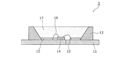
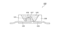
- FIG. 13 is a cross-sectional view showing a conventional semiconductor light emitting device disclosed in Patent Document 1.
- FIG. 13 is a cross-sectional view showing a conventional semiconductor light emitting device disclosed in Patent Document 1.
- a conventional semiconductor light emitting device 100 includes a semiconductor light emitting element 101 that emits ultraviolet light, blue light, or green light disposed in a container 108 in which electrical terminals 102 and 103 are embedded.
- a material 105 (cast epoxy resin layer) containing luminescent material particles 106 (inorganic luminescent material pigment) covers the inside of the container 108 so as to fill the semiconductor light emitting device 101.
- the electrode of the semiconductor light emitting element 101 is electrically connected to the electrical terminal 103 by a gold wire 107.
- a white LED light source is generally a combination of a blue LED and a green phosphor or a yellow phosphor, and a phosphor with excellent light emission characteristics and energy conversion efficiency is required to achieve high efficiency and high color rendering.
- Common phosphors used in white LEDs are fine crystal particles using rare earth ions as an activator, and many are chemically stable.
- quantum dot phosphors fine particles with a diameter of several nanometers to several tens of nanometers called quantum dot phosphors. It is expected as a new phosphor material containing no rare earth.
- the quantum dot phosphor can obtain a fluorescence spectrum in a desired wavelength band in the visible light region by controlling the particle diameter even with fine particles of the same material by the quantum size effect.
- it is light absorption and fluorescence by a band edge, since it shows a high external quantum efficiency of about 90%, a white LED having high efficiency and high color rendering can be provided.
- the quantum dot phosphor has a small particle size, the proportion of atoms occupying the surface of the fine particles increases, so many of them have low chemical stability, especially in excitation fluorescence in a high temperature environment.
- a major problem was that the photo-oxidation reaction on the phosphor surface progressed, causing a rapid decrease in luminous efficiency.
- the container containing the resin layer containing the quantum dot phosphor is configured like the container 108 described in Patent Document 1, and the heat of the cast epoxy resin layer is Because the conductivity is small, the resin layer becomes hot due to heat generation due to the Stokes loss of the quantum dot phosphor in the region away from the heat sink package and the frame resin layer, resulting in deterioration of the quantum dot phosphor and lowering the luminous efficiency. There is a problem.
- the present invention has been made to solve such a problem, and a highly reliable semiconductor light emitting device capable of suppressing a temperature rise of semiconductor fine particles such as a quantum dot phosphor and suppressing a decrease in light emission efficiency.
- the purpose is to provide.
- a first semiconductor light emitting device includes a package made of a resin having a recess, a lead frame exposed on the bottom surface of the recess, and a semiconductor installed on the lead frame in the recess.
- the first resin layer includes semiconductor fine particles having an excitation fluorescence spectrum that changes according to the particle diameter, and the first resin layer is made of a water-soluble or water-dispersible material.
- the semiconductor fine particles can be emulsified with the first resin layer, and the first resin layer containing the semiconductor fine particles can be formed with high density and high uniformity. Furthermore, since the first resin layer can be formed on the exposed lead frame, the heat dissipation of the first resin layer can be improved. As a result, the temperature rise of the semiconductor fine particles can be suppressed to prevent a decrease in the light emission efficiency, so that a semiconductor light emitting device with high efficiency, high color rendering properties and high reliability can be provided.
- the first semiconductor light emitting device further includes a metal reflection film formed on the side surface and the bottom surface of the recess, and the first resin layer is formed so as to cover the metal reflection film. preferable.
- the heat dissipation of the first resin layer can be further improved, and a more reliable semiconductor light emitting device can be provided.
- the semiconductor fine particles have a layer structure of two or more layers, and the outermost layer is a hydrophobic layer.
- the semiconductor fine particles are easily trapped in the main chain skeleton of the water-soluble resin by the hydrophobic interaction, so that the semiconductor fine particles can be dispersed and held in the first resin layer with higher density and higher uniformity. Thereby, it is possible to provide a semiconductor light emitting device with high efficiency and high color rendering without light unevenness.
- the first resin layer is preferably one of an acrylic resin, an epoxy resin, or a fluorine resin.
- the first resin layer has oxygen resistance and moisture resistance, a highly efficient and high color rendering semiconductor light emitting device can be provided.
- the second resin layer may be configured to include light scattering particles that scatter visible light.
- the light emitted from the semiconductor light emitting element is scattered back by the second resin layer, and more uniformly irradiated to the first resin layer in the package. Thereby, it is possible to provide a highly efficient and high color rendering semiconductor light emitting device free from light unevenness.
- the light scattering particles are white fine particles that reflect visible light, and the white fine particles preferably have a particle diameter of 100 nm or more.
- the light scattering particles have a particle diameter of 100 nm or more, include a wavelength at which the semiconductor fine particles absorb a part of light emitted by the semiconductor light emitting element. Phosphor fine particles that give an emission spectrum are preferred.
- the light scattering particles convert a part of the light of the semiconductor light emitting element to the longer wavelength side, so that the Stokes loss of the semiconductor fine particles is reduced and the temperature rise can be suppressed. Thereby, a highly efficient and high color rendering semiconductor light emitting device having high reliability can be provided.
- the semiconductor light emitting element emits blue light
- the semiconductor fine particles have red fluorescence
- the light scattering particles are rare earth phosphors having green fluorescence. can do.
- a second semiconductor light emitting device includes a semiconductor light emitting element mounted on a package having a conductive region and a phosphor layer provided in contact with the conductive region. It is composed of semiconductor fine particles having an excitation fluorescence spectrum that changes depending on the diameter, and a transparent resin that disperses and holds the semiconductor fine particles, and the transparent resin is a water-soluble or water-dispersible material. It is produced from a mixed solution of
- the semiconductor fine particles have a layer structure of two or more layers, and the outermost layer is a hydrophobic layer.
- the semiconductor fine particles are easily trapped by the hydrophobic chain in the main chain skeleton of the water-soluble resin, the semiconductor fine particles can be dispersed and held in the transparent resin with high density and high uniformity. Thereby, it is possible to provide a semiconductor light emitting device with high efficiency and high color rendering without light unevenness.
- the phosphor layer is preferably formed by an electrodeposition process.
- the semiconductor fine particles in which the ionic resin is dispersed in the solution can be electrophoresed on the substrate, and the semiconductor fine particles can be dispersed and held in the transparent resin with high density and high uniformity.
- the transparent resin containing the semiconductor fine particles is preferably any one of an acrylic resin, an epoxy resin, and a fluorine resin.
- semiconductor fine particles can be dispersed and contained in a transparent resin having oxygen resistance and moisture resistance. Thereby, a highly efficient and high color rendering semiconductor light emitting device can be provided.
- a light scattering layer is provided on the phosphor layer and the semiconductor light emitting element, and the light scattering layer includes light scattering particles and light scattering particles that scatter visible light. It is preferably composed of a transparent resin that is dispersed and held.
- the light emitted from the semiconductor light emitting element is scattered back by the light scattering layer, and is uniformly irradiated to the phosphor layer provided in the package.
- the light scattering fine particles contained in the light scattering layer are white fine particles that reflect visible light, and preferably have a particle diameter of 100 nm or more.
- the light scattering particles have a particle diameter of 100 nm or more, absorb part of the light emitted from the semiconductor light emitting element, and are included in the phosphor layer. It is preferable that the phosphor fine particles give an emission spectrum including a wavelength to be absorbed.
- the semiconductor light emitting element emits blue light
- the phosphor layer is a semiconductor fine particle having red fluorescence
- the light scattering particle is a rare earth phosphor having green fluorescence. Can be configured.
- a second method for manufacturing a semiconductor light emitting device wherein a metal reflective film is formed on an inner wall of a package having a conductive region except for at least a portion where a semiconductor light emitting element and a wire are connected.
- a phosphor layer is formed on the metal reflective film by an electrodeposition process while maintaining electrical insulation between the electrodes, and a light scattering layer is formed on the phosphor layer.
- the phosphor layer is in contact with the metal reflective film having a good thermal conductivity in a large area, the temperature rise of the phosphor layer can be suppressed. Thereby, it is possible to manufacture a semiconductor light emitting device having high reliability, high efficiency and high color rendering.
- the present invention since the temperature rise of the semiconductor fluorescent fine particles (quantum dot phosphor) can be suppressed, a semiconductor light emitting device having high reliability, high efficiency, and high color rendering can be provided.
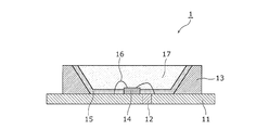
- FIG. 1 is a schematic cross-sectional view of a semiconductor light-emitting device according to Embodiment 1 of the present invention.
- FIG. 2 is a schematic view showing a water-solubilization process of the epoxy resin used in the semiconductor light emitting device according to Embodiment 1 of the present invention.
- FIG. 3 is a schematic diagram showing how the quantum dot phosphor according to the present invention is captured by a resin.
- FIG. 4 is a schematic cross-sectional view of the quantum dot phosphor in the semiconductor light emitting device according to Embodiment 2 of the present invention.
- FIG. 5 is a schematic cross-sectional view of a semiconductor light emitting device according to Embodiment 3 of the present invention.
- FIG. 6 is a schematic diagram for explaining an electrodeposition process in the semiconductor light emitting device according to Embodiment 3 of the present invention.
- FIG. 7A is a cross-sectional view of the light reflecting resin layer forming step in the method for manufacturing a semiconductor light emitting device according to Embodiment 3 of the present invention.
- FIG. 7B is a cross-sectional view of the phosphor layer forming step in the method for manufacturing a semiconductor light emitting device according to Embodiment 3 of the present invention.
- FIG. 7C is a cross-sectional view of the semiconductor light-emitting element mounting step in the method for manufacturing a semiconductor light-emitting device according to Embodiment 3 of the present invention.
- FIG. 7A is a cross-sectional view of the light reflecting resin layer forming step in the method for manufacturing a semiconductor light emitting device according to Embodiment 3 of the present invention.
- FIG. 7B is a cross-sectional view of the phosphor layer forming step in the method for manufacturing
- FIG. 7D is a cross-sectional view of the wire bonding step in the method for manufacturing a semiconductor light emitting device according to Embodiment 3 of the present invention.
- FIG. 8A is a cross-sectional view of the semiconductor light-emitting element mounting step in the method for manufacturing a semiconductor light-emitting device according to Embodiment 4 of the present invention.
- FIG. 8B is a cross-sectional view of the phosphor layer forming step in the method for manufacturing a semiconductor light emitting device according to Embodiment 4 of the present invention.
- FIG. 8C is a cross-sectional view of the insulating protective film removing step in the method for manufacturing a semiconductor light emitting device according to Embodiment 4 of the present invention.
- FIG. 8A is a cross-sectional view of the semiconductor light-emitting element mounting step in the method for manufacturing a semiconductor light-emitting device according to Embodiment 4 of the present invention.
- FIG. 8B is a cross-sectional view of
- FIG. 9 is a schematic cross-sectional view of a semiconductor light-emitting device according to Embodiment 5 of the present invention.
- FIG. 10 is a schematic cross-sectional view of a semiconductor light emitting device according to a modification of the fifth embodiment of the present invention.
- FIG. 11 is a schematic cross-sectional view of a semiconductor light-emitting device according to Embodiment 8 of the present invention.
- FIG. 12 is a schematic cross-sectional view of a semiconductor light-emitting device according to Embodiment 9 of the present invention.
- FIG. 13 is a cross-sectional view of a conventional semiconductor light emitting device.
- FIG. 1 is a schematic cross-sectional view of a semiconductor light-emitting device according to Embodiment 1 of the present invention.
- a lead frame type package is used as the package.
- the semiconductor light emitting device 1 according to Embodiment 1 is a white LED light source that emits white light.
- the semiconductor light emitting device 1 includes a package (container) having a recess made of light reflecting resin layers 12 and 13, a lead frame 11 exposed on the bottom surface of the recess, and a lead frame 11 in the recess.
- the semiconductor light-emitting element 14 installed in the substrate, the phosphor layer 15 (first resin layer) formed so as to cover the bottom surface in the recess, and the resin formed on the phosphor layer 15 and the semiconductor light-emitting element 14.
- a layer 17 (second resin layer).
- the semiconductor light emitting element 14 in the present embodiment is an LED made of a bare chip, and is mounted in a predetermined area on the lead frame 11.
- the P electrode and the N electrode of the semiconductor light emitting element 14 are in electrical contact with the lead frame 11 by a gold wire 16.
- the phosphor layer 15 is formed on the exposed lead frame 11 in the package. That is, the phosphor layer 15 is formed so as to be in contact with the conductive region that becomes the heat sink of the lead frame 11. Thereby, the heat dissipation of the phosphor layer 15 can be improved.
- the phosphor layer 15 is formed outside the contact area of the gold wire 16 and the area where the semiconductor light emitting element 14 is mounted.
- the phosphor layer 15 in the present embodiment is formed not only on the bottom surface of the recess of the package but also on the side surface of the recess (the inner surface of the light reflecting resin layer 13) so as to coat the inner surface of the recess of the package. Are formed with substantially the same film thickness.
- the cup-shaped package is constituted by the lead frame 11 and the light reflecting resin layer 13.
- the resin layer 17 is made of a transparent resin and is filled in the package as a sealing resin.
- the resin layer 17 in this Embodiment is comprised only with transparent resin.
- the phosphor layer 15 is made of a water-soluble or water-dispersible resin material and a quantum dot phosphor. Specifically, the phosphor layer 15 has a configuration in which quantum dot phosphors are uniformly dispersed in a transparent resin having oxygen barrier properties and moisture resistance.
- an epoxy resin is used as the transparent resin for the phosphor layer 15.
- Epoxy resin is a material having oxygen permeability of 2 to 3 digits lower than that of silicone resin, and is one of resins that can be easily water-soluble or water-dispersible by amination. Further, as the transparent resin for the phosphor layer 15, a resin other than the epoxy resin can be used.
- a transparent resin made of a fluorine resin or an acrylic resin also has a high oxygen barrier property and a high moisture resistance.
- a material having oxygen barrier properties and moisture resistance as the transparent resin of the phosphor layer 15, it is possible to effectively suppress the photooxidation reaction of the quantum dot phosphor.
- semiconductor fine particles having an excitation fluorescence spectrum that varies depending on the particle diameter can be used as the quantum dot phosphor. In the quantum dot phosphor, the excitation fluorescence spectrum changes according to the particle diameter, and the emission wavelength of the quantum dot phosphor can be adjusted by changing the particle diameter.
- Preparation of the phosphor layer 15 according to the present invention includes a dispersion step of dispersing the quantum dot phosphor (phosphor fine particles) in a resin solution and a resin formation step. A description will be given below for each process.
- the phosphor layer 15 according to the present invention is formed of a water-soluble or water-dispersible resin solvent.
- a water-soluble resin has an ionized or electrically polar part of the resin molecular skeleton in an aqueous solution, and the polar part and ionized region of the resin molecule are stabilized by hydration, so it is dissolved or dispersed in water to become an emulsion. can do.
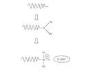
- FIG. 2 is a diagram showing a water-solubilization process of the epoxy resin used in the present embodiment. As shown in FIG. 2, it can ionize by aminating the terminal of an epoxy resin and neutralizing with an acid. In this embodiment, acetic acid is used as the acid to be neutralized.
- FIG. 3 is a diagram showing the capture of the quantum dot phosphor by a resin.
- a quantum dot phosphor 21 by adding a quantum dot phosphor 21 to a resin solution 20 neutralized with acetic acid 25, the main chain 23 of the epoxy resin solvent molecules having an aminated cation portion 22 becomes a quantum dot phosphor 24. To capture. Thereby, the quantum dot phosphor 21 can be uniformly dispersed in the resin solution 20.
- the particle size of the phosphor fine particles is large, the phosphor fine particles are not sufficiently trapped in the main chain of the resin solvent molecules and settle or settle in the resin solution 20.
- the particle diameter of commercially available rare earth phosphors is 1 ⁇ m to 100 ⁇ m, which is much larger than the size of resin solvent molecules. Therefore, many resin molecules are required to capture one rare-earth phosphor fine particle, and the dispersion concentration decreases or the sedimentation phenomenon occurs in the water-soluble resin, resulting in uneven brightness and light emission. End up.
- the particle diameter of the quantum dot phosphor is about 1 nm to 20 nm and the size is equal to or smaller than that of the water-soluble resin molecule, it can be dispersed uniformly and at a high concentration in the resin solution.
- the semiconductor fine particles used in the present embodiment are quantum dot phosphors having a diameter of about 1 nm to 10 nm with InP as a nucleus.
- any phosphor material may be used as long as it does not dissolve in water.
- Known cadmium quantum dot phosphors and chalcogenide fine particles may be used.
- a spray method (spray method) is used for the resin coating process.
- the spraying method is a method in which a resin solvent that captures fine particles is applied to an object by spraying a mist, and a resin coating can be formed on any object that has good wettability. Is possible.
- the lead frame type package has a resin region and a metal region.
- the package surface is made hydrophilic by plasma treatment using a mixed gas of Ar and H 2 or a mixed gas of Ar and O 2 . did.
- the resin is cured by spraying a resin solvent containing the quantum dot phosphor on the lead frame 11 in the form of a mist to heat the resin.
- the phosphor layer 15 can be formed only at the locations.
- a resin layer 17 made of a transparent silicone resin is filled in the package.
- the resin layer 17 is intended to protect the semiconductor light emitting element 14 and the phosphor layer 15, but the structure for protecting the semiconductor light emitting element 14 and the phosphor layer 15 is not necessarily the resin layer 17.
- the resin layer 17 instead of filling the resin layer 17, it may be configured to be sealed with a transparent glass plate.
- the lead frame type package is used.
- a ceramic package or a metal package formed of ceramic may be used.
- the quantum dot phosphor and the resin material in the phosphor layer 15 can be emulsified, the quantum dot phosphor is densely and highly uniform in the phosphor layer 15. Can be dispersed. Furthermore, since the phosphor layer 15 can be formed on the exposed lead frame 11, the heat dissipation of the phosphor layer 15 can be improved. Thereby, since the temperature rise of the fluorescent substance layer 15 can be suppressed and the fall of luminous efficiency can be suppressed, a highly efficient, high color rendering property, and highly reliable semiconductor light-emitting device can be provided.
- quantum dot phosphors have a two-layer or three-layer structure called a core-shell structure for the purpose of improving luminous efficiency and reliability, but for efficient dispersion in water-soluble resin solvents.
- a core-shell structure for the purpose of improving luminous efficiency and reliability, but for efficient dispersion in water-soluble resin solvents.
- the chemical properties of the outermost layer of the quantum dot are important.
- the terminal of the resin skeleton is ionized or polar functionalized, but the molecular skeleton is composed of hydrocarbons such as an alkyl main chain and is almost polar. Does not have. This means that the interaction with water is small and behaves as a hydrophobic group.
- the quantum dot phosphor to be trapped in the main chain of the water-soluble resin, the outermost layer of the quantum dot is nonpolar or polar. It is necessary to be composed of a weak ligand or layer. With this configuration, the quantum dot phosphor is easily trapped in the resin main chain by hydrophobic interaction, and thus can be emulsified and uniformly dispersed in the resin aqueous solution.
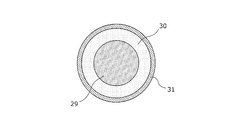
- FIG. 4 is a cross-sectional configuration diagram of the quantum dot phosphor in the semiconductor light emitting device according to Embodiment 2 of the present invention.
- FIG. 4 since it is the same as that of Embodiment 1 about components other than the structure of quantum dot fluorescent substance, detailed description is abbreviate
- the quantum dot phosphor used in the second embodiment has a three-layer structure, and a core 29 made of InP and a shell layer 30 made of ZnS formed so as to cover the outside of the core 29. And have. Further, as an outermost layer, a ligand layer 31 in which octane hydrocarbon is bonded as a ligand is provided outside the shell layer 30. Thus, the ligand layer 31 made of hydrocarbon is provided as the hydrophobic layer having strong hydrophobicity in the outermost layer, so that the quantum dot phosphor is efficiently trapped in the main chain of the resin molecule in the aqueous solution. .
- the quantum dot phosphor can be emulsified with high concentration and high uniformity.
- the quantum dot phosphor can be dispersed in the resin solution with higher density and higher uniformity, so that a highly efficient and high color rendering semiconductor light emitting device free from light unevenness can be provided.
- the quantum dot phosphor Since the quantum dot phosphor has a small core diameter, it has a core-shell layer-ligand layer multilayer structure of about 10 nm to 100 nm, and the size of the quantum dot phosphor is dispersed in the resin solution. Will not be affected. For this reason, the shell layer 30 and the ligand layer 31 are not particularly limited as long as the material structure is not decomposed by water. Since the ligand layer 31 preferably has a large hydrophobic interaction with the resin solution, a molecule having an alkyl main chain is preferable. On the other hand, in order to improve the dispersibility in the resin solution, a smaller molecular weight is preferable. Specifically, since it is necessary to be able to exist as a liquid at room temperature, the number of carbon atoms is preferably 15 or less.
- the quantum dot phosphor is a phosphor having a feature that the fluorescence wavelength varies with the particle diameter. Therefore, when the semiconductor light emitting element 14 emits blue light, in order to produce the phosphor layer 15 (phosphor film) that gives white fluorescence, a quantum dot phosphor having a particle diameter that gives red fluorescence and green fluorescence. What is necessary is just to produce the fluorescent substance layer containing both of the quantum dot fluorescent substance which has a particle diameter which gives.
- the particle diameter of the InP-based quantum dot phosphor according to the present embodiment is about 5 nm to 8 nm in the case of the green phosphor, and the largest particle diameter is about 10 nm to 20 nm in the case of the red fluorescence. Therefore, in the case of quantum dot phosphors, both red phosphors, green phosphors, and smaller blue phosphors, from the viewpoint of particle size, all quantum dot phosphors that fluoresce in the visible light region are exposed to the resin solution. Dispersion is possible. Therefore, a desired luminescent color can be obtained by mixing quantum dot phosphors having a plurality of particle sizes (different fluorescence wavelengths) in a resin solution.
- FIG. 5 is a schematic cross-sectional view of a semiconductor light emitting device according to Embodiment 3 of the present invention.
- the semiconductor light emitting device 3 is configured by the lead frame 11 and the light reflecting resin layers 12 and 13 as in the first embodiment.
- a semiconductor light emitting element 14 is mounted on the lead frame 11, and the P electrode and the N electrode of the semiconductor light emitting element 14 are electrically connected to the lead frame 11 by a gold wire 16.
- Embodiment 1 is different from Embodiment 1 in the configuration of the phosphor layer 15.
- the phosphor layer 15 in the present embodiment is formed only at the bottom of the recess of the package. That is, the phosphor layer 15 is provided on the conductive region that becomes the heat sink of the package, except for the contact region of the gold wire 16 and the region where the semiconductor light emitting element 14 is mounted. Accordingly, the phosphor layer 15 is formed only on the lowermost part on the inner side surface of the light reflecting resin layer 13, and the phosphor layer 15 is not formed on most of the inclined surface.
- the cup-shaped package made up of the lead frame 11 and the light reflecting resin layer 13 is filled with a resin layer 17 made of a transparent resin as in the first embodiment.
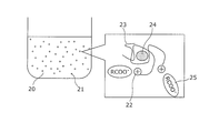
- the semiconductor light emitting device 3 was manufactured using an electrodeposition method as a method of forming a resin layer (phosphor layer 15) from a resin solution.
- the electrodeposition method is a method in which a voltage is applied to an object immersed in a resin solution, and an ionic resin solvent that captures the quantum dot phosphor is formed on the surface of the object by electrophoresis and electrochemical reaction. .
- the electrodeposition method since a film is formed by an electrochemical reaction, it is possible to form a resin layer with a uniform film thickness, and a uniform film can be formed even if the object to be coated has a complicated surface shape.
- the principle is an electrochemical reaction, a resin layer cannot be formed by an electrodeposition method unless it is a conductive object.
- the phosphor layer 15 was formed using a cationic electrodeposition method.
- FIG. 6 is a schematic view of the electrodeposition process.
- the epoxy resin is aminated (cationized), and an electrodeposition film is formed on the conductive region of the lead frame by using the lead frame as the cathode electrode 42.
- the resin solvent is an acid solvent
- the object to be coated becomes an anode, which is an anionic electrodeposition method.
- the resin coating film obtained by these methods is finally formed through a drying process and a curing process.
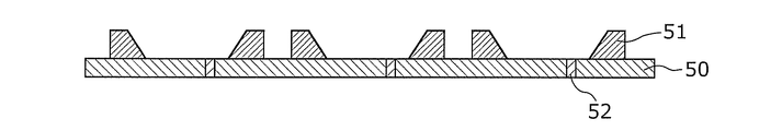
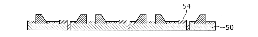
- FIGS. 7A to 7D are diagrams showing a part of a process cross-sectional view in the method for manufacturing a semiconductor light emitting device according to the third embodiment.
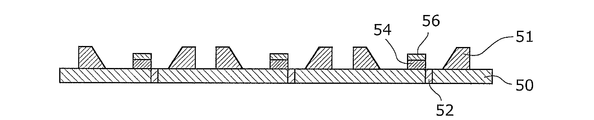
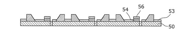
- light reflecting resin layers 51 and 52 are formed on the lead frame 50.
- a resist for insulation protection is applied in advance to the mounting region of the semiconductor light emitting element 14 and the contact region with the gold wire 16 on the lead frame 50, and the electrodeposition process shown in FIG.
- the phosphor layer 53 containing the quantum dot phosphor is formed on the conductive region of the lead frame 50.
- the phosphor layer 53 is not electrodeposited on the light reflecting resin layers 51 and 52. Thereafter, after removing the resist, drying and thermosetting are performed.
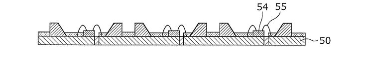
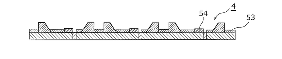
- the semiconductor light emitting device 54 is mounted in a predetermined region on the lead frame 50, and as shown in FIG. 7D, the electrodes of the semiconductor light emitting device 54 and the electrode terminals of the lead frame 50 are formed by the gold wires 55. (Not shown) is electrically connected (wire bonding).
- the quantum dot phosphor in which the ionic resin is dispersed in the solution is electrophoresed on the lead frame.
- the quantum dot phosphor can be dispersed and held in the transparent resin with high density and high uniformity. Thereby, it is possible to provide a semiconductor light emitting device with high efficiency and high color rendering without light unevenness.
- the phosphor layer can be formed by electrodeposition bath after the semiconductor light emitting element is mounted and the wire is connected.
- the electrodeposition bath is immersed in a state where a potential difference is generated between the P electrode side and the N electrode side, an electrochemical reaction occurs due to the potential difference between the electrodes, and migration or dissolution of the electrode material occurs. Therefore, it is preferable to short-circuit the P side (P electrode) and the N side (N electrode) of the semiconductor light emitting element so that all the conductive regions have the same potential.
- the resin layer (phosphor layer 15) is preferably formed after the semiconductor light emitting element 14 is mounted.
- the semiconductor light-emitting element 54 is mounted on the lead frame 50 in a state where it is covered with an insulating protective film 56 such as a heat-resistant resist in advance.
- the resin layer (phosphor layer 53) containing the quantum dot phosphor is formed. This will be specifically described below.
- a resist as an insulating protective film 56 is applied by spin coating on the wafer before the semiconductor light emitting element 54 is separated into chips.
- the insulating protective film 56 is formed on the upper electrode of the semiconductor light emitting element 54.
- the semiconductor light emitting element 54 in which the insulating protective film 56 is formed is mounted on the lead frame 50 in which the light reflecting resin layers 51 and 52 are formed.
- the lead frame 50 in the state shown in FIG. 8A is immersed in an electrodeposition bath, so that quantum dot fluorescence is formed on the conductive region of the lead frame 50 as shown in FIG. 8B.
- the phosphor layer 53 containing the body can be formed.
- the phosphor layer 53 is not electrodeposited.
- the semiconductor light emitting device 4 having a structure in which only the upper portion of the semiconductor light emitting element 54 is not electrodeposited by the phosphor layer 53 can be realized. it can.
- the phosphor layer including the quantum dot phosphor can be formed only on the package and not in contact with the semiconductor light emitting element that becomes high temperature. Thereby, a highly reliable and high color rendering semiconductor light emitting device can be provided.
- a semiconductor light emitting device having the same configuration as that of the semiconductor light emitting device 3 according to the third embodiment shown in FIG. 5 can be manufactured.
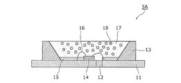
- FIG. 9 shows a schematic cross-sectional view of a semiconductor light emitting device according to Embodiment 5 of the present invention.
- the semiconductor light emitting device 5 according to the fifth embodiment includes light scattering particles 18 that scatter visible light in the resin layer 17 in the semiconductor light emitting device 1 according to the first embodiment shown in FIG. Is a structure in which is dispersed.
- white light particles made of titanium dioxide (TiO 2 ) that reflect visible light are used as the light scattering particles 18.
- light scattering particles 18 such as TiO 2 fine particles are mixed in advance with a transparent resin such as a silicone resin, and after the phosphor layer 15 is spray-coated, the transparent resin is placed in the package. It can be produced by injection.
- FIG. 10 shows the configuration of the semiconductor light emitting device 5A when the phosphor layer 15 is formed by electrodeposition.
- FIG. 10 is a schematic cross-sectional view of a semiconductor light emitting device according to a modification of the fifth embodiment of the present invention.
- the electrodeposition method can also be prepared by injecting a silicone resin containing light scattering particles 18 such as TiO 2 fine particles into the package after forming the phosphor layer 15 as in the spraying method.
- a silicone resin containing light scattering particles 18 such as TiO 2 fine particles
- the thermosetting temperature of a silicone resin is about 150 degreeC, it is preferable to use resin with high heat resistance, such as an epoxy resin and a fluorine resin, as resin which comprises the fluorescent substance layer 15.
- FIG. 10 shows the configuration of the semiconductor light emitting device 5A when the phosphor layer 15 is formed by electrodeposition.
- FIG. 10 is a schematic cross-sectional view of a semiconductor light emitting device according to a modification of the fifth embodiment of the present invention.
- the semiconductor light emitting device since the light scattering particles 18 are dispersed in the resin layer 17, the light emitted from the semiconductor light emitting element 14 is scattered by the resin layer 17 and fluorescent.
- the body layer 15 is irradiated more uniformly. Thereby, it is possible to provide a highly efficient and high color rendering semiconductor light emitting device free from light unevenness.
- a silicone resin is used as the resin layer 17, but the resin constituting the resin layer 17 is transparent and is lower than the melting temperature or decomposition temperature of the resin forming the phosphor layer 15. If it is resin hardened
- TiO 2 fine particles are used as the light scattering particles 18, but fine particles made of other materials may be used as long as they are white fine particles.
- lead white carbonate called lead white (2PbCO 3 ⁇ Pb (OH) 2
- ZnO called zinc white
- the light scattering particles 18 are a material that does not absorb the emission wavelength of the semiconductor light emitting element 14 and the fluorescence wavelength of the quantum dot phosphor. In order to reflect light from the semiconductor light emitting element 14 more efficiently, it is desirable that the particle diameter of the light scattering particles 18 is as large as the wavelength of the light emitted from the semiconductor light emitting element 14.
- the constituent material of the light scattering particles 18 is transparent to the light emitted from the semiconductor light emitting element 14.
- the size (particle diameter) of the fine particles is about the wavelength of the semiconductor light emitting element 14, a light scattering phenomenon called Mie scattering occurs.
- a light scattering phenomenon called Mie scattering occurs.
- white particles made of a transparent material are scattered white.
- the particle diameter of the light scattering particles 18 needs to be about one-fourth to one wavelength of the wavelength of light emitted from the semiconductor light-emitting element 14. Accordingly, the visible light region of the white LED is 400 nm to 700 nm, and the light scattering particle 18 needs to strongly reflect the blue light having the shortest wavelength, so the particle diameter of the light scattering particle 18 is about 100 nm or more. It is preferable that
- the light scattering particles 18 are white fine particles that reflect visible light, and the white fine particles have a particle diameter of 100 nm or more. It will scatter light without absorbing light. Thereby, it is possible to provide a highly efficient and high color rendering semiconductor light emitting device free from light unevenness.
- the light scattering particles 18 of the resin layer 17 absorb light from the semiconductor light emitting element 14 and use the excitation light of the quantum dot phosphor as fluorescence.
- a light scattering phosphor made of a rare earth phosphor that radiates may also be used. That is, the light scattering particle 18 may be a phosphor that absorbs a part of the light emitted by the semiconductor light emitting element 14 and gives an emission spectrum including a wavelength that the quantum dot phosphor absorbs.
- the particle diameter of the light scattering particles 18 made of a phosphor is 100 nm or more.
- a YAG (yttrium, aluminum, garnet) phosphor that is a rare earth phosphor is used as the light scattering phosphor that is the light scattering particle 18.
- the resin layer of the phosphor layer 15 contained a red quantum dot phosphor that gives red fluorescence.
- a part of the blue light emitted by the semiconductor light emitting element 14 that emits blue light is absorbed by the YAG phosphor of the resin layer 17, and yellowish green Give fluorescence.
- the red quantum dot phosphor absorbs a part of the yellow-green light emission and gives red fluorescence.
- the light scattering particles 18 need not be limited to the YAG phosphor, and may be any phosphor that can absorb the blue light of the semiconductor light emitting element 14 and convert the wavelength.
- the fluorescence spectrum of the YAG phosphor extends to a long wavelength region of 700 nm or more with almost no visibility, and although the color rendering is improved by combining with the red quantum dot phosphor, the luminous efficiency (lm / W) hardly changes. .
- a phosphor such as a sialon (SiAlON) phosphor that has a fluorescence spectrum centered on green with high visibility and whose fluorescence spectrum does not spread on the long wavelength side of 700 nm or more has a luminous efficiency (lm / W) is higher than the YAG phosphor. Therefore, by using the SiAlON phosphor as the light scattering particles 18 and combining with the red quantum dot phosphor, white light having high color rendering properties and high luminous efficiency (lm / W) can be obtained.
- SiAlON sialon
- the quantum dot phosphor converts the wavelength from green to red, the Stokes loss is smaller than that from blue to red, and the calorific value of the quantum dot phosphor is reduced. That is, since the light scattering particle 18 converts part of the light of the semiconductor light emitting element 14 to the longer wavelength side, the Stokes loss of the quantum dot phosphor is reduced. Thereby, since the temperature rise of a quantum dot can further be suppressed, the highly reliable color rendering semiconductor light-emitting device which has high reliability can be provided.
- FIG. 11 is a schematic cross-sectional view of a semiconductor light-emitting device according to Embodiment 8 of the present invention.
- the phosphor layer 15 is formed on the highly reflective metal film in order to efficiently extract the fluorescence obtained from the phosphor layer 15 from the semiconductor light emitting device.
- a metallic reflective film 19 made of gloss Ag is formed on the lead frame 11 and the insulating resin layer 62 by electroless plating.
- the metal reflection film 19 is formed on the inner wall of the package having the conductive region of the lead frame 11 except for the portion where the semiconductor light emitting element 14 and the wire connection are made.
- the metal reflection film 19 must prevent the P electrode and the N electrode in the semiconductor light emitting element 14 from being short-circuited.
- a region where Ag is not plated is formed by protecting the insulating resin layer 61 with a resist or the like in advance, thereby ensuring the insulation of the device.
- the metal reflection film 19 is formed on the side surface and the bottom surface of the recess of the package.
- the phosphor layer 15 is formed on the surface of the metal reflection film 19 by electrodeposition using the metal reflection film 19 made of Ag plating as an electrode.
- the semiconductor light emitting device since the phosphor layer 15 is formed on the metal reflection film 19, the heat dissipation of the phosphor layer 15 can be further improved. Therefore, a highly reliable semiconductor light emitting device can be provided.
- the metal reflection film 19 can be formed also on the insulating resin layer 62. Therefore, the phosphor layer 15 can be easily formed on the inner side surface of the package by using the electrodeposition method using the metal reflective film 19 as an electrode. Moreover, since the metal reflective film 19 has higher thermal conductivity than the insulating resin layer 62, the heat dissipation of the phosphor layer 15 is improved, and the temperature rise of the quantum dot phosphor can be suppressed.
- the electrical insulation between the electrodes of the semiconductor light emitting element 14 is maintained on the surface of the metal reflective film 19 formed on the inner surface of the package.
- the phosphor layer 15 is formed by the electrodeposition method, the phosphor layer 15 comes into contact with the metal reflective film 19 having a good thermal conductivity in a large area. Thereby, since the temperature rise of the phosphor layer 15 can be effectively suppressed, it is possible to manufacture a semiconductor light emitting device having high reliability, high efficiency and high color rendering.
- FIG. 12 is a schematic cross-sectional view of a semiconductor light-emitting device according to Embodiment 9 of the present invention.
- the semiconductor light emitting element 14 is one of the highest temperature regions in the semiconductor light emitting device of the present invention.
- the thermal conductivity of the resin layer 17 is increased, and the heat of the semiconductor light emitting element 14 is transmitted to the phosphor layer 15 through the resin layer 17.
- the temperature of the phosphor layer 15 rises.
- the junction temperature may exceed 150 ° C., so that the deterioration of the phosphor layer 15 is accelerated.
- heat generated by the phosphor layer 15 during wavelength conversion is dissipated to the conductive region of the lead frame 11 and at the same time, heat from the semiconductor light emitting element 14 is not easily transmitted to the phosphor layer 15.
- the semiconductor light emitting element 14 is covered with a transparent resin layer 70 that does not contain ceramic fine particles.
- the transparent resin layer 70 is made of only a silicone resin, and is formed in a dome shape so as to cover the semiconductor light emitting element 14.
- the transparent resin layer 70 does not contain ceramic fine particles, the thermal conductivity of the transparent resin layer 70 is kept lower than the thermal conductivity of the resin layer 17, and the heat of the semiconductor light emitting element 14 is reduced. Conduction upward (resin layer 17 side) can be suppressed. As a result, most of the heat of the semiconductor light emitting element 14 is dissipated through the lead frame 11, so that the temperature rise of the phosphor layer 15 can be suppressed even when the semiconductor light emitting element 14 is in a high output operation. It becomes.
- the semiconductor light emitting device it is possible to achieve both heat dissipation of the phosphor layer 15 during wavelength conversion and heat shielding from the semiconductor light emitting element 14 to the phosphor layer 15. Therefore, the temperature rise of the phosphor layer 15 can be suppressed even in a high output operation. Thereby, a highly reliable semiconductor light emitting device can be provided.
- a metal reflection film 19 is vapor-deposited as a highly reflective metal film on the inner wall of a region (concave portion) surrounded by the insulating resin layer 62 formed on the lead frame 11, and a fluorescence containing a quantum dot phosphor on the metal reflection film 19.
- a body layer 15 is deposited.
- the semiconductor light emitting element 14 is mounted in a predetermined region on the lead frame 11, the semiconductor light emitting element 14 and the gold wire 16 are connected by wire bonding, and then a transparent resin made of silicone resin so as to cover the semiconductor light emitting element 14.
- Layer 70 is formed by coating. In this state, defoaming is performed once. And shaping
- the resin layer 17 is formed by injecting a silicone resin containing the light scattering particles 18 onto the phosphor layer 15 and the transparent resin layer 70 so as to fill the concave portion of the insulating resin layer 62.
- the semiconductor light emitting device 9 having the configuration as shown in FIG. 12 can be manufactured.
- the semiconductor light emitting element 14 and the lead frame 11 are connected by the gold wire 16 and the transparent resin layer 70 is formed before the phosphor layer 15 is deposited on the metal reflective film 19. Thereafter, the phosphor layer 15 may be formed.
- the semiconductor light emitting device according to the present invention has been described based on the embodiment, but the present invention is not limited to the above embodiment.
- the LED is exemplified as the semiconductor light emitting element 14, but a semiconductor light emitting element such as a semiconductor laser, an organic EL (Electro Luminescence), or an inorganic EL may be used.
- a semiconductor light emitting element such as a semiconductor laser, an organic EL (Electro Luminescence), or an inorganic EL may be used.
- the blue LED is used as the semiconductor light emitting element 14, but the present invention is not limited to this. Further, the combination of the emission color of the semiconductor light emitting element 14 and the fluorescence color of the quantum dot phosphor of the phosphor layer 15 is not limited to the above embodiment.
- white light may be emitted by a blue LED that emits blue light and yellow phosphor particles that are excited by blue light and emit yellow light.
- an ultraviolet LED that emits ultraviolet light having a shorter wavelength than a blue LED, and blue phosphor particles, green phosphor particles, and red fluorescence that are mainly excited by ultraviolet light to emit blue light, red light, and green light.
- the body particles may be configured to emit white light. Thereby, a semiconductor light emitting device with high color rendering can be realized.
- a semiconductor light emitting device with high reliability, high efficiency, and high color rendering can be realized, so that it is widely useful as a white LED light source for display devices, lighting devices, and the like.
Landscapes
- Engineering & Computer Science (AREA)
- Microelectronics & Electronic Packaging (AREA)
- Computer Hardware Design (AREA)
- Power Engineering (AREA)
- Manufacturing & Machinery (AREA)
- Led Device Packages (AREA)
- Luminescent Compositions (AREA)
Abstract
本発明の半導体発光装置(1)は、凹部を有する樹脂からなるパッケージと、凹部の底面に露出したリードフレーム(11)と、凹部内のリードフレーム(11)に設置された半導体発光素子(14)と、凹部内の底面を覆うように形成された蛍光体層(15)と、蛍光体層(15)および半導体発光素子(14)の上に形成された樹脂層(17)とを備え、蛍光体層(15)は、粒子径に応じて変化する励起蛍光スペクトルを有する半導体微粒子を含み、蛍光体層(15)は、水溶性または水分散性を有する材料からなる。
Description
本発明は、半導体発光装置に関し、特に蛍光体層に量子ドット蛍光体を用いた半導体発光装置に関するものである。
照明用または液晶ディスプレイバックライト用などの光源として高輝度白色LED(Light Emitting Diode)が用いられており、光源の高効率化および高演色性化の取り組みが行われている。白色LEDは、例えば、青色光を放出する半導体発光素子と、緑色蛍光体、黄色蛍光体または赤色蛍光体とを適宜組み合わせることで実現している。蛍光体の種類は、無機蛍光体、有機蛍光体、あるいは、半導体から構成される量子ドット蛍光体がある。無機蛍光体を用いた白色LEDの例として、特許文献1のようなものがある。
図13は、特許文献1に開示された従来の半導体発光装置を示す断面図である。
図13に示すように、従来の半導体発光装置100は、紫外光、青色光あるいは緑色光を放出する半導体発光素子101が、電気端子102、103が埋め込まれた容器108内に配置されたものであり、さらに、半導体発光素子101を埋めるように発光物質粒子106(無機の発光物質顔料)を含有する材料105(注型エポキシ樹脂層)が容器108内を覆っている。なお、半導体発光素子101の電極は、金ワイヤー107によって電気端子103と電気的に接続されている。
LED光源は小型で省電力なため、ディスプレイデバイスや照明装置のキーデバイスとして用いられており、高輝度白色LEDの高効率化および高演色性化の取り組みが行われている。白色LED光源は、青色LEDと緑色蛍光体や黄色蛍光体との組み合わせが一般的であり、高効率および高演色性の実現には発光特性やエネルギー変換効率の優れた蛍光体が求められている。白色LEDに用いられる一般的な蛍光体は、希土類イオンを付活剤とした結晶微粒子であり、化学的に安定なものが多い。しかし、これらの蛍光体の光吸収効率は希土類の濃度に比例している一方で、濃度が高すぎると濃度消光によって発光効率の低下が生じるため、80%以上の高い量子効率を実現するのが困難であった。
そこで、バンド端における光吸収や発光を直接利用することで高い量子効率を実現する半導体蛍光微粒子が多数提案されており、特に量子ドット蛍光体と呼ばれる直径が数nmから数十nmの微粒子が、希土類を含まない新しい蛍光体材料として期待されている。量子ドット蛍光体は、量子サイズ効果によって同一材料の微粒子でも粒子径を制御することで可視光線領域において所望の波長帯の蛍光スペクトルを得ることが出来る。また、バンド端による光吸収や蛍光であるため、90%程度の高い外部量子効率を示すことから、高効率および高演色性を有する白色LEDを提供することができる。
しかし、量子ドット蛍光体は粒子径が小さいため、微粒子の表面を占める原子の割合が多くなることから、化学的安定性の低いものが多く、特に高温環境下での励起蛍光においては、量子ドット蛍光体表面の光酸化反応が進行し、急激な発光効率の低下を引き起こすことが大きな課題であった。
また、この量子ドット蛍光体を用いて白色LEDを形成する場合、量子ドット蛍光体を含む樹脂層を収容する容器が特許文献1記載の容器108のような構成では、注型エポキシ樹脂層の熱伝導率が小さいため、ヒートシンクとなるパッケージおよびフレーム樹脂層から離れた領域では、量子ドット蛍光体のストークスロスによる発熱によって樹脂層が高温化し、量子ドット蛍光体の劣化が生じて発光効率が低下するという課題がある。
本発明は、このような課題を解決するためになされたものであり、量子ドット蛍光体等の半導体微粒子の温度上昇を抑制し、発光効率の低下を抑えることができる信頼性の高い半導体発光装置を提供することを目的とする。
上記の課題を解決するために、本発明に係る第1の半導体発光装置は、凹部を有する樹脂からなるパッケージと、凹部の底面に露出したリードフレームと、凹部内のリードフレームに設置された半導体発光素子と、凹部内の底面を覆うように形成された第1の樹脂層と、蛍光体層および半導体発光素子の上に形成された第2の樹脂層とを備え、第1の樹脂層は、粒子径に応じて変化する励起蛍光スペクトルを有する半導体微粒子を含み、第1の樹脂層は、水溶性または水分散性を有する材料からなることを特徴とする。
この構成により、半導体微粒子を第1の樹脂層とエマルジョン化させることができ、半導体微粒子を含む第1の樹脂層を高密度および高均一で形成することができる。さらに、露出したリードフレーム上に第1の樹脂層を形成することができるので、第1の樹脂層の放熱性を向上させることができる。これにより、半導体微粒子の温度上昇を抑制して発光効率の低下を抑えることができるので、高効率および高演色性でかつ高信頼性の半導体発光装置を提供できる。
さらに、本発明に係る第1の半導体発光装置において、凹部の側面と底面とに形成された金属反射膜をさらに備え、第1の樹脂層は金属反射膜を覆うように形成されていることが好ましい。
この構成により、第1の樹脂層の放熱性をさらに向上させることができ、さらに信頼性の高い半導体発光装置を提供できる。
さらに、本発明に係る第1の半導体発光装置において、半導体微粒子は、2層以上の層構造を有しており、最外層は疎水性層であることが好ましい。
この構成により、半導体微粒子が水溶性樹脂の主鎖骨格に疎水性相互作用により捕捉されやすくなるため、半導体微粒子をさらに高密度で高均一に第1の樹脂層に分散保持させることができる。これにより、光ムラのない高効率および高演色性の半導体発光装置を提供できる。
さらに、本発明に係る第1の半導体発光装置において、第1の樹脂層は、アクリル系樹脂またはエポキシ系樹脂またはフッ素系樹脂のいずれかであることが好ましい。
この構成により、第1の樹脂層が耐酸素性および耐湿性を有するので、高効率および高演色性の半導体発光装置を提供できる。
さらに、本発明に係る第1の半導体発光装置において、第2の樹脂層は、可視光線を散乱する光散乱粒子を含むように構成してもよい。
この構成により、半導体発光素子が放射する光は、第2の樹脂層によって後方にも散乱され、パッケージ内の第1の樹脂層に対してより均一に照射される。これにより、光ムラの無い高効率で高演色性の半導体発光装置を提供できる。
さらに、本発明に係る第1の半導体発光装置において、光散乱粒子は可視光線を反射する白色微粒子であって、当該白色微粒子の粒子径が100nm以上であることが好ましい。
この構成により、白色微粒子が光を吸収することなく光を散乱することから、光ムラの無い高効率で高演色性の半導体発光装置を提供できる。
さらに、本発明に係る第1の半導体発光装置において、光散乱粒子は、粒子径が100nm以上であって、半導体発光素子が放射する光の一部を吸収し、半導体微粒子が吸収する波長を含む発光スペクトルを与える蛍光体微粒子であることが好ましい。
この構成により、光散乱粒子が半導体発光素子の光の一部を長波長側に波長変換するので、半導体微粒子のストークスロスが小さくなり温度上昇を抑制することができる。これにより、高い信頼性を有する高効率で高演色性の半導体発光装置を提供できる。
さらに、本発明に係る第1の半導体発光装置において、半導体発光素子は青色の光を放射し、半導体微粒子は赤色蛍光を有し、光散乱粒子は緑色蛍光を有する希土類蛍光体であるように構成することができる。
この構成により、より演色性の高い白色光を実現することができるとともに、半導体微粒子は希土類蛍光体の緑色蛍光を吸収して赤色光を蛍光発光するため、半導体微粒子のストークスロスが小さくなり、温度上昇を一層抑制することができる。これにより、高い信頼性を有する高効率で高演色性の半導体発光装置を提供できる。
また、本発明に係る第2の半導体発光装置は、導電性領域を有するパッケージに実装された半導体発光素子と導電性領域に接して設けられた蛍光体層とを有し、蛍光体層は粒子径に応じて変化する励起蛍光スペクトルを有する半導体微粒子と、当該半導体微粒子を分散保持する透明樹脂とから構成され、当該透明樹脂は水溶性または水分散性の材料であり、半導体微粒子と透明樹脂との混合溶液から生成されることを特徴とする。
この構成によれば、半導体微粒子を水溶性樹脂溶剤とエマルジョン化させることで高密度および高均一な蛍光体層の形成が可能と成り、かつヒートシンクとなる導電性領域上に蛍光体層を設けることで、蛍光体層の放熱性が向上する。これにより、高効率および高演色性でかつ高信頼性の半導体発光装置を提供できる。
さらに、本発明に係る第2の半導体発光装置において、半導体微粒子は2層以上の層構造を有しており、最外層は疎水性層であることが好ましい。
この構成によれば、半導体微粒子が水溶性樹脂の主鎖骨格に疎水性相互作用により捕捉されやすくなるため、高密度で高均一に半導体微粒子を透明樹脂中に分散保持させることができる。これにより、光ムラのない高効率および高演色性の半導体発光装置を提供できる。
さらに、本発明に係る第2の半導体発光装置において、蛍光体層は電着工程によって形成されることが好ましい。
この構成によれば、イオン性樹脂が溶液中に分散した半導体微粒子を基板上へ電気的に泳動させることができ、高密度で高均一に半導体微粒子を透明樹脂に分散保持させることができる。これにより、光ムラの無い高効率および高演色性の半導体発光装置を提供できる。
さらに、本発明に係る第2の半導体発光装置において、半導体微粒子を含有する透明樹脂はアクリル系樹脂、エポキシ系樹脂またはフッ素系樹脂のいずれかであることが好ましい。
この構成であれば、耐酸素性および耐湿性を有する透明樹脂に半導体微粒子を分散含有させることができる。これにより、高効率および高演色性の半導体発光装置を提供できる。
さらに、本発明に係る第2の半導体発光装置において、蛍光体層および半導体発光素子の上部に光散乱層が設けられており、光散乱層は可視光線を散乱する光散乱粒子と光散乱粒子を分散保持する透明樹脂とから構成されていることが好ましい。
この構成によれば、半導体発光素子が放射する光は、光散乱層によって後方にも散乱され、パッケージ内に設けられた蛍光体層に均一に照射される。これにより、光ムラの無い高効率で高演色性の半導体発光装置を提供できる。
さらに、本発明に係る第2の半導体発光装置において、光散乱層に含有する光散乱微粒子は可視光線を反射する白色微粒子であって、粒子径が100nm以上であることが好ましい。
この構成によれば、白色微粒子が光を吸収することなく光を散乱することから、光ムラの無い高効率で高演色性の半導体発光装置を提供できる。
さらに、本発明に係る第2の半導体発光装置において、光散乱粒子は粒子径が100nm以上であって、半導体発光素子が放射する光の一部を吸収し、蛍光体層に含まれる半導体発光粒子が吸収する波長を含む発光スペクトルを与える蛍光体微粒子であることが好ましい。
この構成によれば、散乱微粒子が半導体発光素子の光の一部を長波長側に波長変換するので、半導体微粒子のストークスロスが小さくなり温度上昇を抑制することができる。これにより、高い信頼性を有する高効率で高演色性の半導体発光装置を提供できる。
さらに、本発明に係る第2の半導体発光装置において、半導体発光素子は青色を発光し、蛍光体層は赤色蛍光を有する半導体微粒子であり、光散乱粒子は緑色蛍光を有する希土類蛍光体であるように構成することができる。
この構成であれば、より演色性の高い白色光を実現することができるとともに、半導体微粒子は希土類蛍光体の緑色蛍光を吸収して赤色発光をするため、半導体微粒子のストークスロスが小さくなり、温度上昇を抑制することができる。これにより、高い信頼性を有する高効率で高演色性の半導体発光装置を提供できる。
また、本発明に係る第2の半導体発光装置の製造方法は、導電性領域を有するパッケージの内壁に少なくとも半導体発光素子およびワイヤー接続を行う箇所を除いて金属反射膜を形成し、半導体発光素子の電極間の電気的な絶縁を保持した状態で蛍光体層を金属反射膜上に電着工程によって形成し、蛍光体層の上に光散乱層を形成することを特徴とする。
この構成によれば、蛍光体層が熱伝導率の良い金属反射膜と大きな面積で接しているため、蛍光体層の温度上昇を抑制することができる。これにより、高い信頼性を有し、高効率で高演色性の半導体発光装置を製造することができる。
本発明によれば、半導体蛍光微粒子(量子ドット蛍光体)の温度上昇を抑制することができるので、高信頼性、高効率および高演色性を有する半導体発光装置を提供することが出来る。
以下、図面を参照しながら、本発明の実施の形態に係る半導体発光装置を説明するが、本発明は、請求の範囲の記載に基づいて特定される。よって、以下の実施の形態における構成要素のうち、請求項に記載されていない構成要素は、本発明の課題を達成するのに必ずしも必要ではないが、より好ましい形態を構成するものとして説明される。なお、各図において、同じ構成要素には同じ符号を付しており、その詳しい説明は省略又は簡略化する。
(実施の形態1)
まず、本発明の実施の形態1に係る半導体発光装置1について、図1を用いて説明する。図1は、本発明の実施の形態1に係る半導体発光装置の断面概略図である。
まず、本発明の実施の形態1に係る半導体発光装置1について、図1を用いて説明する。図1は、本発明の実施の形態1に係る半導体発光装置の断面概略図である。
実施の形態1ではパッケージとしてリードフレーム型パッケージを用いた。また、実施の形態1に係る半導体発光装置1は、白色光を放出する白色LED光源である。
本発明の実施の形態1に係る半導体発光装置1は、光反射樹脂層12、13からなる凹部を有するパッケージ(容器)と、凹部の底面に露出したリードフレーム11と、凹部内のリードフレーム11に設置された半導体発光素子14と、凹部内の底面を覆うように形成された蛍光体層15(第1の樹脂層)と、蛍光体層15および半導体発光素子14の上に形成された樹脂層17(第2の樹脂層)とを備える。
本実施の形態における半導体発光素子14は、ベアチップからなるLEDであり、リードフレーム11上の所定領域に実装されている。半導体発光素子14のP電極およびN電極は、金ワイヤー16によってリードフレーム11との電気的接点が取られている。
蛍光体層15は、パッケージ内において、露出したリードフレーム11上に形成されている。すなわち、蛍光体層15は、リードフレーム11のヒートシンクとなる導電性領域上に接するように形成されている。これにより、蛍光体層15の放熱性を向上させることができる。なお、蛍光体層15は、金ワイヤー16の接点領域および半導体発光素子14を実装する領域以外に形成されている。
また、本実施の形態における蛍光体層15は、パッケージの凹部の底面だけではなく、凹部の側面(光反射樹脂層13の内面)にも形成されており、パッケージの凹部の内面を被膜するように略同一膜厚で形成されている。
なお、本実施の形態において、カップ状のパッケージは、リードフレーム11と光反射樹脂層13とによって構成されている。樹脂層17は、透明樹脂によって構成されており、封止樹脂としてパッケージの内部に充填されている。なお、本実施の形態における樹脂層17は、透明樹脂のみによって構成されている。
蛍光体層15は、水溶性または水分散性を有する樹脂材料と量子ドット蛍光体とからなる。具体的に、蛍光体層15は、酸素バリア性および耐湿性を有する透明樹脂に、量子ドット蛍光体を均一に分散させた構成である。本実施の形態では、蛍光体層15の透明樹脂としては、エポキシ系樹脂を用いた。エポキシ系樹脂はシリコーン樹脂に比べると酸素透過性が2桁から3桁ほど低い材料であり、アミン化することで水溶性化または水分散性化が容易な樹脂の一つである。また、蛍光体層15の透明樹脂としてはエポキシ系樹脂以外の樹脂も用いることができる。例えば、フッ素系樹脂やアクリル系樹脂からなる透明樹脂も高い酸素バリア性および高い耐湿性を有している。このように、蛍光体層15の透明樹脂として、酸素バリア性および耐湿性を有する材料を用いることにより、量子ドット蛍光体の光酸化反応を効果的に抑制することが可能である。また、蛍光体層15における量子ドット蛍光体としては、粒子径によって異なる励起蛍光スペクトルを有する半導体微粒子を用いることができる。量子ドット蛍光体は粒子径に応じて励起蛍光スペクトルが変化し、粒子径を変えることで量子ドット蛍光体の発光波長を調整することができる。
本発明に係る蛍光体層15の作製は、量子ドット蛍光体(蛍光体微粒子)を樹脂溶液に分散する分散工程と、樹脂形成工程とからなる。以下工程ごとに説明を行う。
まず、量子ドット蛍光体の分散工程について説明する。上述のように、本発明に係る蛍光体層15は、水溶性または水分散性の樹脂溶剤から形成されることを特徴としている。水溶性樹脂は水溶液中で樹脂分子骨格の一部がイオン化または電気的極性を有しており、樹脂分子の極性箇所やイオン化領域が水和によって安定化するため水に溶解または分散してエマルジョン化することができる。
図2は、本実施の形態で用いたエポキシ樹脂の水溶性化過程を示す図である。図2に示すように、エポキシ樹脂の末端をアミン化し、酸で中和することでイオン化することができる。本実施の形態では、中和する酸として酢酸を用いた。
図3は、量子ドット蛍光体の樹脂による捕捉を示す図である。図3に示すように、酢酸25によって中和した樹脂溶液20に量子ドット蛍光体21を加えることで、アミン化した陽イオン部22を有するエポキシ樹脂溶剤分子の主鎖23が量子ドット蛍光体24を捕捉する。これにより、量子ドット蛍光体21を均一に樹脂溶液20中に分散させることができる。
このとき、蛍光体微粒子の粒径が大きいと、蛍光体微粒子は、樹脂溶剤分子の主鎖に十分に捕捉されずに樹脂溶液20に沈降したり沈殿したりする。
ここで、市販の希土類蛍光体の粒子径は1μm~100μmであり、樹脂溶剤分子の大きさよりもはるかに大きい。従って、1つの希土類蛍光体の微粒子を捕捉するのに多くの樹脂分子が必要となり、分散濃度が低下したり水溶性樹脂中での沈降現象が起こったりして、輝度ムラや発光ムラが発生してしまう。
一方、量子ドット蛍光体の粒子径は1nm~20nm程度であり水溶性樹脂分子と同等、またはそれ以下のサイズであるため、樹脂溶液中に均一にかつ高濃度で分散させることが可能となる。
本実施の形態で用いた半導体微粒子は、InPを核とする直径1nmから10nm程度の量子ドット蛍光体であるが、蛍光体の材料としては水に溶解しないものであればよく、InP以外にも公知のカドミウム系量子ドット蛍光体やカルコゲナイド系微粒子であっても良い。
次に、蛍光体層15の樹脂形成工程について説明する。実施の形態1では樹脂の塗膜工程に噴霧法(スプレー法)を用いた。噴霧法は微粒子を捕捉した樹脂溶剤を霧状のスプレーで被塗物に塗布する方法であり、被塗物の濡れ性が良いものであれば、どんなものにでも樹脂塗膜を形成することが可能である。
リードフレーム型パッケージには樹脂領域と金属領域とがあり、樹脂水溶液の濡れ性を更に高めるために、ArとH2の混合ガスやArとO2の混合ガスによるプラズマ処理によりパッケージ表面を親水化した。
量子ドット蛍光体を含有した樹脂溶媒をリードフレーム11上に霧状にして噴きつけて加熱を行うことにより樹脂を硬化させる。
なお、リードフレーム11の半導体発光素子14を実装する領域や金ワイヤー16を接続する領域をレジストで保護しておき、蛍光体をスプレーした後、レジストを除去し、樹脂を熱硬化させることで所望の場所にのみ蛍光体層15を形成することができる。
また、実施の形態1では半導体発光素子14や蛍光体層15がむき出しになることを防ぐために、透明なシリコーン樹脂で構成された樹脂層17をパッケージ内に充填している。なお、樹脂層17は、半導体発光素子14および蛍光体層15の保護を目的としているが、半導体発光素子14および蛍光体層15を保護する構成としては、必ずしも樹脂層17である必要はない。例えば、樹脂層17を充填する替わりに透明ガラス板によって封止する構成であってもかまわない。また、本実施の形態ではリードフレーム型パッケージを用いたが、蛍光体層15を形成する上では、セラミックによって成形されたセラミックパッケージや金属パッケージであっても良い。
以上、本発明の実施の形態1によれば、蛍光体層15における量子ドット蛍光体と樹脂材料とをエマルジョン化させることができるので、蛍光体層15において量子ドット蛍光体を高密度および高均一で分散させることができる。さらに、露出したリードフレーム11上に蛍光体層15を形成することができるので、蛍光体層15の放熱性を向上させることができる。これにより、蛍光体層15の温度上昇を抑制して発光効率の低下を抑えることができるので、高効率および高演色性、かつ高信頼性の半導体発光装置を提供できる。
(実施の形態2)
次に、本発明の実施の形態2に係る半導体発光装置について説明する。
次に、本発明の実施の形態2に係る半導体発光装置について説明する。
量子ドット蛍光体の多くは、発光効率の向上や信頼性向上を目的としたコア-シェル構造と呼ばれる2層または3層構造を有しているが、水溶性樹脂溶剤へ効率良く分散をさせるためには、量子ドットの最外層の化学的特性が重要となる。
図3で示したように、水溶性樹脂や水分散性樹脂は、樹脂骨格の末端がイオン化または極性官能基化しているが、分子骨格はアルキル主鎖のような炭化水素から構成され、ほとんど極性を有していない。これは水との相互作用が小さく疎水性基として振舞うことを意味しており、量子ドット蛍光体が水溶性樹脂の主鎖に捕捉されるためには、量子ドットの最外層は無極性や極性の弱い配位子や層から構成されることが必要となる。この構成によって量子ドット蛍光体は疎水性相互作用により樹脂主鎖に捕捉されやすくなるので、樹脂水溶液中にエマルジョン化して均一に分散することが可能となる。
図4は、本発明の実施の形態2に係る半導体発光装置における量子ドット蛍光体の断面構成図である。なお、量子ドット蛍光体の構成以外の構成要素については実施の形態1と同様であるので、詳しい説明は省略又は簡略化する。
図4に示すように、実施の形態2で用いた量子ドット蛍光体は、3層構造であり、InPからなるコア29と、コア29の外側を覆うように形成されたZnSから成るシェル層30とを有している。また、最外層として、シェル層30の外側には、オクタン系の炭化水素を配位子として結合させたリガンド層31が設けられている。このように、最外層に疎水性の強い疎水性層として炭化水素からなるリガンド層31が設けられていることにより、水溶液中において、効率良く量子ドット蛍光体が樹脂分子の主鎖に捕捉される。その結果、高濃度で高均一に量子ドット蛍光体をエマルジョン化させることが可能となる。これにより、量子ドット蛍光体をさらに高密度で高均一に樹脂溶液中に分散させることができるので、光ムラのない高効率および高演色性の半導体発光装置を提供できる。
なお、量子ドット蛍光体はコア直径が小さいため、コア-シェル層-リガンド層の多層構造を有していても約10nm~100nm程度であり、量子ドット蛍光体の大きさが樹脂溶液への分散に影響を与えることはない。このため、シェル層30やリガンド層31も水によって分解されない材料構成であれば、特に限定されるものではない。リガンド層31としては、樹脂溶液との疎水性相互作用が大きいものが好ましいため、アルキル主鎖をもつ分子が良い。一方で、樹脂溶液への分散性を高める上では、分子量が小さいほうが好ましい。具体的には、室温で液体として存在することが出来ることが必要であるため、炭素数が15個以下とすることが好ましい。
また、量子ドット蛍光体は先述の通り、粒子径で蛍光波長が変化する特徴を有する蛍光体である。そのため、半導体発光素子14が青色光を発する場合、白色蛍光を与える蛍光体層15(蛍光体フィルム)を作製するためには、赤の蛍光を与える粒子径をもつ量子ドット蛍光体および緑の蛍光を与える粒子径をもつ量子ドット蛍光体の両方を含有する蛍光体層を作製すればよい。
本実施の形態に係るInP系量子ドット蛍光体の粒子径は、緑色蛍光体の場合が約5nm~8nm程度であり、赤色蛍光の場合が最も粒子径が大きくなり10nm~20nm程度である。よって量子ドット蛍光体であれば赤色蛍光体も緑色蛍光体もそれより小さい青色蛍光体においても、粒子サイズの観点から言えば可視光線領域に蛍光を与えるすべての量子ドット蛍光体が樹脂溶液への分散が可能となる。よって、複数の粒子径を有する(蛍光波長の異なる)量子ドット蛍光体を樹脂溶液中に混合することで所望の発光色を得ることができる。
(実施の形態3)
次に、本発明の実施の形態3に係る半導体発光装置3について、図5を用いて説明する。図5は、本発明の実施の形態3に係る半導体発光装置の断面概略図である。
次に、本発明の実施の形態3に係る半導体発光装置3について、図5を用いて説明する。図5は、本発明の実施の形態3に係る半導体発光装置の断面概略図である。
図5に示すように、実施の形態3に係る半導体発光装置3は、実施の形態1と同様に、リードフレーム11と光反射樹脂層12、13によって構成されている。リードフレーム11上には半導体発光素子14が実装されており、半導体発光素子14のP電極およびN電極は、リードフレーム11に対して金ワイヤー16で電気的接点が取られている。
本実施の形態が実施の形態1と異なる点は、蛍光体層15の構成である。本実施の形態における蛍光体層15は、パッケージの凹部の底部にのみ形成されている。すなわち、蛍光体層15は、パッケージのヒートシンクとなる導電性領域上において、金ワイヤー16の接点領域および半導体発光素子14を実装する領域以外に設けられている。従って、光反射樹脂層13の内側面には最下部のみに蛍光体層15形成されており、傾斜面の大部分には蛍光体層15は形成されていない。なお、リードフレーム11と光反射樹脂層13とからなるカップ状のパッケージの内部には、実施の形態1と同様に、透明樹脂からなる樹脂層17が充填されている。
また、本実施の形態に係る半導体発光装置3は、樹脂溶液から樹脂層(蛍光体層15)を形成する方法として電着法を用いて製造した。電着法は、樹脂溶液に浸した被塗物に電圧を印加し、量子ドット蛍光体を捕捉したイオン性樹脂溶剤を電気泳動および電気化学反応によって被塗物表面に被膜形成を行う方法である。電着法では、電気化学反応によって被膜を形成するため、均一な膜厚の樹脂層形成が可能であり、被塗物が複雑な表面形状を有していても均一に塗膜ができる。ただし、電気化学反応を原理としているため、導電性被塗物でなければ電着法による樹脂層形成はできない。
本実施の形態において、蛍光体層15は、カチオン電着法を用いて形成した。図6は、その電着工程の概略図である。
図6に示すように、エポキシ系の樹脂溶液に量子ドット蛍光体41を分散させたエポキシ系樹脂溶液40に、カソード電極42である被塗物であるリードフレームと、対向電極であるアノード電極43とを浸す。エポキシ系樹脂はアミン化(陽イオン化)しており、リードフレームをカソード電極42にすることで電着膜がリードフレームの導電性領域上に成膜される。一方、樹脂溶剤が酸系であれば、被塗物はアノードとなりアニオン型電着法となる。これらの方法で得られた樹脂塗膜は、乾燥工程および硬化工程を経て最終形成される。
図7A~図7Dは、実施の形態3に係る半導体発光装置の製造方法における工程断面図の一部を示す図である。
まず、図7Aに示すように、リードフレーム50に、光反射樹脂層51、52を形成する。次に、リードフレーム50上における半導体発光素子14の実装領域および金ワイヤー16との接点領域に予め絶縁保護するためのレジストを塗布しておき、図6に示す電着工程によって、図7Bに示すように、リードフレーム50の導電性領域上に量子ドット蛍光体を含有した蛍光体層53を成膜する。このとき、光反射樹脂層51、52には蛍光体層53は電着されない。その後、レジストを除去した後に、乾燥と熱硬化とを行う。
次に、図7Cに示すように、リードフレーム50上の所定領域に半導体発光素子54を実装し、図7Dに示すように、金ワイヤー55によって半導体発光素子54の電極とリードフレーム50の電極端子(不図示)とを電気的に接続(ワイヤーボンディング)する。
以上、本実施の形態に係る半導体発光装置によれば、蛍光体層15を電着工程によって形成するので、イオン性樹脂が溶液中に分散した量子ドット蛍光体をリードフレーム上へ電気的に泳動させることができ、量子ドット蛍光体を高密度で高均一に透明樹脂に分散保持させることができる。これにより、光ムラの無い高効率および高演色性の半導体発光装置を提供できる。
なお、実施の形態1および3は、半導体発光素子を実装してワイヤーを接続した後に電着浴にて蛍光体層を形成することもできる。ただし、P電極側とN電極側とに電位差が発生した状態で電着浴に浸した場合、電極間同士の電位差によって電気化学反応が起こり、電極物質のマイグレーションや溶解が発生する。よって、導電性領域はすべて同電位となるように半導体発光素子のP側(P電極)とN側(N電極)とを短絡させることが好ましい。
(実施の形態4)
次に、本発明の実施の形態4に係る半導体発光装置4について説明する。本実施の形態に係る半導体発光装置4の構成は、実施の形態1、3に係る半導体発光装置と同様であるので、具体的な構成の説明は省略する。
次に、本発明の実施の形態4に係る半導体発光装置4について説明する。本実施の形態に係る半導体発光装置4の構成は、実施の形態1、3に係る半導体発光装置と同様であるので、具体的な構成の説明は省略する。
リードフレーム型パッケージは半導体発光素子を実装する際に半田のリフロー工程などで高温にさらされるため、量子ドット蛍光体を分散保持する樹脂層が熱によって劣化して変色や剥がれなどの不具合が生じる場合がある。このため、実施の形態1および3に係る半導体発光装置の構造において、樹脂層(蛍光体層15)の形成は、半導体発光素子14の実装後に行うことが好ましい。
そこで、実施の形態4では、図8A~図8Cに示すように、あらかじめ半導体発光素子54を耐熱性レジストなどの絶縁保護膜56によって被覆した状態で、リードフレーム50上に実装して電着工程で量子ドット蛍光体を含有した樹脂層(蛍光体層53)を成膜している。以下、具体的に説明する。
まず、半導体発光素子54をチップに分離する前のウェハに対して絶縁保護膜56としてのレジストをスピンコートで塗布する。本実施の形態では、半導体発光素子54の上部電極上に絶縁保護膜56を形成した。その後、ダイシングによってチップ分離を行った後、図8Aに示すように、光反射樹脂層51、52が形成されたリードフレーム50に、絶縁保護膜56が形成された半導体発光素子54を実装する。
次に、上述同様の電着法を用いて、図8Aに示す状態のリードフレーム50を電着浴に浸すことにより、図8Bに示すように、リードフレーム50の導電性領域上に量子ドット蛍光体を含有した蛍光体層53を形成することができる。このとき、半導体発光素子54の上部電極は絶縁保護膜56によって絶縁されているため、蛍光体層53が電着されることはない。
その後、図8Cに示すように、絶縁保護膜56(レジスト)を除去することにより、半導体発光素子54の上部のみが蛍光体層53によって電着形成されない構造の半導体発光装置4を実現することができる。
この構成であれば、量子ドット蛍光体を含む蛍光体層を、パッケージ上のみに形成し、高温になる半導体発光素子とは接しないように形成することができる。これにより、高信頼性で高演色性の半導体発光装置を提供できる。なお、本実施の形態における製造方法では、図5に示す実施の形態3に係る半導体発光装置3と同様の構成の半導体発光装置を製造することができる。
(実施の形態5)
次に、本発明の実施の形態5に係る半導体発光装置5について、図9を用いて説明する。
次に、本発明の実施の形態5に係る半導体発光装置5について、図9を用いて説明する。
実施の形態5では、発光ムラを抑制するため、実施の形態1から3で形成した量子ドット蛍光体を分散した蛍光体層の上部に、蛍光体層に対する均一な光照射を目的とした光散乱層を設けた。図9に、本発明の実施の形態5に係る半導体発光装置の断面概略図を示す。
図9に示すように、実施の形態5に係る半導体発光装置5は、図1に示す実施の形態1に係る半導体発光装置1における樹脂層17の中に、可視光線を散乱する光散乱粒子18を分散させた構造である。本実施の形態では、光散乱粒子18として、二酸化チタン(TiO2)からなる可視光線を反射する白色微粒子を用いた。本実施の形態における構造は、例えば、予めTiO2微粒子などの光散乱粒子18をシリコーン樹脂などの透明樹脂に混合しておき、蛍光体層15をスプレー塗布した後に、当該透明樹脂をパッケージ内に注入することにより作製することができる。
また、蛍光体層15を電着法によって形成した場合の半導体発光装置5Aの構成を図10に示す。図10は、本発明の実施の形態5の変形例に係る半導体発光装置の断面概略図である。電着法においても、噴霧法と同様に蛍光体層15を形成した後にTiO2微粒子などの光散乱粒子18を含有するシリコーン樹脂をパッケージ内に注入することによって作製することができる。なお、シリコーン樹脂の熱硬化温度が150℃程度であるため、蛍光体層15を構成する樹脂としては、エポキシ樹脂やフッ素系樹脂といった耐熱性の高い樹脂を用いることが好ましい。
このように、本実施の形態に係る半導体発光装置によれば、樹脂層17に光散乱粒子18が分散されているので、半導体発光素子14から放出される光は樹脂層17によって散乱されて蛍光体層15に対してより均一に照射されることになる。これにより、光ムラの無い高効率で高演色性の半導体発光装置を提供できる。
なお、本実施の形態では、樹脂層17としてシリコーン樹脂を用いているが、樹脂層17を構成する樹脂は、透明であり、蛍光体層15を形成する樹脂の溶融温度または分解温度よりも低い温度で硬化する樹脂であれば、特に限定は無い。
また、本実施の形態では、光散乱粒子18としてTiO2微粒子を用いたが、白色微粒子であれば他の材料からなる微粒子を用いてもよい。例えば、鉛白と呼ばれる鉛の塩基性炭酸塩(2PbCO3・Pb(OH)2)、亜鉛華とよばれるZnO、炭酸カルシウム(CaCO3)、または硫酸カルシウム水和物(CaSO4・2H2O)などを光散乱粒子18として用いることができる。
(実施の形態6)
次に、本発明の実施の形態6に係る半導体発光装置について説明する。本実施の形態に係る半導体発光装置の構成は、例えば、図9または図10に示す実施の形態5と同様の構成とすることができる。
次に、本発明の実施の形態6に係る半導体発光装置について説明する。本実施の形態に係る半導体発光装置の構成は、例えば、図9または図10に示す実施の形態5と同様の構成とすることができる。
実施の形態5において、光散乱粒子18は、半導体発光素子14の発光波長および量子ドット蛍光体の蛍光波長を吸収しない材料であることが前提となる。さらに効率良く半導体発光素子14からの光を反射するためには、光散乱粒子18の粒子径は半導体発光素子14が発する光の波長程度の大きさであることが望ましい。
光散乱粒子18の構成材料は、半導体発光素子14が発する光に対して透明であるが、微粒子のサイズ(粒子径)が半導体発光素子14の波長程度になるとミー散乱と呼ばれる光の散乱現象が生じるため、透明な材料からなる微粒子であっても白色の散乱がなされる。
しかし、微粒子が更に小さくなると、レイリー散乱と呼ばれる光散乱に支配されるようになり、散乱強度は粒子径の6乗に比例するため、粒子が小さすぎると再び微粒子は半導体発光素子14の光に対して透明となる。
このため、効率良く光を散乱させるためには、光散乱粒子18の粒子径は、半導体発光素子14が発する光の波長の4分の1程度から1波長程度の大きさが必要である。従って、白色LEDの可視光線領域は400nm~700nmであり、光散乱粒子18としては、最も短波長の青色の光を強く反射させる必要があることから、光散乱粒子18の粒子径は約100nm以上とすることが好ましい。
このように、本実施の形態に係る半導体発光装置によれば、光散乱粒子18が可視光線を反射する白色微粒子であって、当該白色微粒子の粒子径が100nm以上であるので、白色微粒子は、光を吸収することなく光を散乱することになる。これにより、光ムラの無い高効率で高演色性の半導体発光装置を提供できる。
(実施の形態7)
次に、本発明の実施の形態7に係る半導体発光装置について説明する。本実施の形態に係る半導体発光装置の構成は、例えば、図9または図10に示す実施の形態5と同様の構成とすることができる。
次に、本発明の実施の形態7に係る半導体発光装置について説明する。本実施の形態に係る半導体発光装置の構成は、例えば、図9または図10に示す実施の形態5と同様の構成とすることができる。
図9または図10に示す実施の形態5に係る半導体発光装置おいて、樹脂層17の光散乱粒子18は、半導体発光素子14からの光を吸収し、量子ドット蛍光体の励起光を蛍光として放射する希土類蛍光体からなる光散乱蛍光体でも良い。すなわち、光散乱粒子18は、半導体発光素子14が放射する光の一部を吸収し、量子ドット蛍光体が吸収する波長を含む発光スペクトルを与える蛍光体であってもよい。また、本実施の形態においても、蛍光体からなる光散乱粒子18の粒子径は100nm以上であることが好ましい。
実施の形態7では、光散乱粒子18である光散乱蛍光体として、希土類蛍光体であるYAG(イットリウム・アルミニウム・ガーネット)蛍光体を用いている。また、蛍光体層15の樹脂層には、赤色蛍光を与える赤色量子ドット蛍光体を含有させた。
このように、本実施の形態に係る半導体発光装置の構成によれば、青色光を発する半導体発光素子14によって発光した青色光の一部は、樹脂層17のYAG蛍光体が吸収し、黄緑色の蛍光を与える。また、赤色量子ドット蛍光体が、その黄緑色発光の一部を吸収し、赤色蛍光を与える。これにより、高い演色性を実現することができる。
なお、光散乱粒子18はYAG蛍光体に限る必要はなく、半導体発光素子14の青色光を吸収し波長変換できる蛍光体であれば良い。YAG蛍光体の蛍光スペクトルは、視感度がほとんど無い700nm以上の長波長領域に及んでおり、赤色量子ドット蛍光体との組み合わせにより演色性は向上するものの発光効率(lm/W)はほとんど変化しない。一方、サイアロン(SiAlON)蛍光体などように、視感度の大きい緑を中心とした蛍光スペクトルを有し、蛍光スペクトルが700nm以上の長波長側に広がっていない蛍光体については、発光効率(lm/W)がYAG蛍光体に比べて高い。よって、SiAlON蛍光体を光散乱粒子18として用い、赤色量子ドット蛍光体と組み合わせることで、高い演色性を有しかつ発光効率(lm/W)の高い白色光を得ることが出来る。
また、この構成であれば、量子ドット蛍光体は緑色から赤色に波長を変換するため青色から赤色に比べてストークスロスが小さく、量子ドット蛍光体の発熱量が小さくなる。すなわち、光散乱粒子18が半導体発光素子14の光の一部を長波長側に波長変換するので、量子ドット蛍光体のストークスロスが小さくなる。これにより、量子ドットの温度上昇を更に抑制することができることから、高い信頼性を有する高演色性の半導体発光装置を提供できる。
(実施の形態8)
次に、本発明の実施の形態8に係る半導体発光装置8について、図11を用いて説明する。図11は、本発明の実施の形態8に係る半導体発光装置の断面概略図である。
次に、本発明の実施の形態8に係る半導体発光装置8について、図11を用いて説明する。図11は、本発明の実施の形態8に係る半導体発光装置の断面概略図である。
実施の形態8では、蛍光体層15から得られる蛍光を効率良く半導体発光装置から取り出すために、蛍光体層15を高反射金属膜上に形成した。
図11に示すように、本実施の形態では、リードフレーム11と絶縁樹脂層62上に無電解メッキ法によって光沢Agからなる金属反射膜19が成膜されている。金属反射膜19は、リードフレーム11の導電性領域を有するパッケージの内壁において、半導体発光素子14およびワイヤー接続を行う箇所を除いて形成されている。
このとき、金属反射膜19によって、半導体発光素子14におけるP電極とN電極とが短絡しないようにしなければならない。実施の形態8では、メッキ処理をする前に予めレジスト等で絶縁樹脂層61上を保護することでAgがメッキされない領域を形成しておき、これにより、デバイスの絶縁性を確保した。本実施の形態において、金属反射膜19は、パッケージの凹部の側面と底面とに形成されている。
また、このAgメッキからなる金属反射膜19を電極にした電着により、金属反射膜19の表面に蛍光体層15が形成されている。
このように、本実施の形態に係る半導体発光装置によれば、蛍光体層15は金属反射膜19上に形成されているので、蛍光体層15の放熱性をさらに向上させることができる。従って、信頼性の高い半導体発光装置を提供できる。
さらに、本実施の形態では、無電解メッキ法を用いているので、絶縁樹脂層62上にも金属反射膜19を形成することができる。従って、金属反射膜19を電極とした電着法を用いることで、パッケージの内側側面にも容易に蛍光体層15を形成することができる。また、金属反射膜19は、絶縁樹脂層62よりも熱伝導率が高いため、蛍光体層15の放熱性が向上し、量子ドット蛍光体の温度上昇を抑制することが可能となる。
また、本実施の形態に係る半導体発光装置の製造方法によれば、パッケージの内面に形成された金属反射膜19の表面上に、半導体発光素子14の電極間の電気的な絶縁を保持した状態で、蛍光体層15を電着法によって形成するので、蛍光体層15が熱伝導率の良い金属反射膜19と大きな面積で接することになる。これにより、蛍光体層15の温度上昇を効果的に抑制することができるので、高い信頼性を有し、高効率で高演色性の半導体発光装置を製造することができる。
(実施の形態9)
次に、本発明の実施の形態9に係る半導体発光装置9について、図12を用いて説明する。図12は、本発明の実施の形態9に係る半導体発光装置の断面概略図である。
次に、本発明の実施の形態9に係る半導体発光装置9について、図12を用いて説明する。図12は、本発明の実施の形態9に係る半導体発光装置の断面概略図である。
半導体発光素子14は、本発明の半導体発光装置において最も高温になる領域の一つである。一方、樹脂層17にセラミック系の光散乱粒子18を含有させると樹脂層17の熱伝導率が増大してしまい、半導体発光素子14の熱が樹脂層17を介して蛍光体層15に伝達して蛍光体層15の温度が上昇してしまう。特に半導体発光素子14を高出力動作させる場合、その接合温度は150℃を超える場合もあるため、蛍光体層15の劣化を加速させることになる。
そこで、本実施の形態では、波長変換時の蛍光体層15の発熱をリードフレーム11の導電性領域に放熱させると同時に、半導体発光素子14からの熱が蛍光体層15に伝わりにくくするために、セラミックス微粒子が含まれない透明樹脂層70によって半導体発光素子14を覆う構成とした。
本実施の形態において、透明樹脂層70は、シリコーン樹脂のみによって構成されており、半導体発光素子14を覆うようにドーム状に形成されている。このように、透明樹脂層70にはセラミック微粒子が含まれていないため、透明樹脂層70の熱伝導率は樹脂層17の熱伝導率よりも低く保たれており、半導体発光素子14の熱が上方(樹脂層17側)に伝導することを抑制することができる。これにより、半導体発光素子14の熱のほとんどがリードフレーム11を介して放熱することになるので、半導体発光素子14が高出力動作であっても蛍光体層15の温度上昇を抑制することが可能となる。
このように、本実施の形態に係る半導体発光装置によれば、波長変換時の蛍光体層15の放熱と、半導体発光素子14から蛍光体層15への熱遮蔽との両立を図ることができることから、高出力動作においても蛍光体層15の温度上昇を抑制できる。これにより、高い信頼性を有する半導体発光装置を提供できる。
次に、本実施の形態における製造方法の一例について、図12を用いて説明する。
まず、リードフレーム11に形成された絶縁樹脂層62で囲まれる領域(凹部)の内壁に高反射金属膜として金属反射膜19を蒸着し、当該金属反射膜19上に量子ドット蛍光体を含む蛍光体層15を堆積させる。
次に、リードフレーム11上の所定領域に半導体発光素子14を実装し、ワイヤーボンディングによって半導体発光素子14と金ワイヤー16とを接続した後、半導体発光素子14を覆うようにシリコーン樹脂からなる透明樹脂層70を塗布形成する。この状態で一度脱泡処理を行う。そして、150℃で30分の熱硬化処理を行うことで、シリコーン樹脂の整形を行う。
次に、絶縁樹脂層62の凹部内を埋めるように、光散乱粒子18を含有したシリコーン樹脂を蛍光体層15および透明樹脂層70の上に注入することによって、樹脂層17を形成する。これにより、図12に示すような構成の半導体発光装置9を製造することができる。
なお、上記製造方法と異なり、金属反射膜19上に蛍光体層15を堆積させる前に、半導体発光素子14とリードフレーム11との金ワイヤー16による接続と、透明樹脂層70の形成とを行い、その後に蛍光体層15を形成してもよい。
以上、本発明に係る半導体発光装置について、実施の形態に基づいて説明したが、本発明は、上記の実施の形態に限定されるものではない。
例えば、上記の実施の形態では、半導体発光素子14としてLEDを例示したが、半導体レーザ、有機EL(Electro Luminescence)又は無機EL等の半導体発光素子を用いてもよい。
また、上記の実施の形態では、半導体発光素子14として青色LEDを用いたが、これに限らない。また、半導体発光素子14の発光色と蛍光体層15の量子ドット蛍光体の蛍光色との組み合わせは、上記の実施の形態に限定されるものではない。例えば、青色光を放出する青色LEDと、青色光により励起されて黄色光を放出する黄色蛍光体粒子とによって白色光を放出するように構成してもよい。あるいは、青色LEDよりも短波長である紫外光を放出する紫外LEDと、主に紫外光により励起されて青色光、赤色光および緑色光を放出する青色蛍光体粒子、緑色蛍光体粒子および赤色蛍光体粒子とによって白色光を放出するように構成してもよい。これにより、演色性の高い半導体発光装置を実現することができる。
その他、本発明の要旨を逸脱しない範囲内で当業者が思いつく各種変形を施したものも本発明の範囲内に含まれる。また、発明の趣旨を逸脱しない範囲で、複数の実施の形態における各構成要素を任意に組み合わせてもよい。
本発明によれば、高い信頼性、高効率および高演色性の半導体発光装置を実現することができるので、ディスプレイデバイスや照明装置等の白色LED光源等として広く有用である。
1、3、4、5、5A、8、9、100 半導体発光装置
11、50 リードフレーム
12、13、51、52 光反射樹脂層
14、54、101 半導体発光素子
15、53 蛍光体層
16、55、107 金ワイヤー
17 樹脂層
18 光散乱粒子
19 金属反射膜
20 樹脂溶液
21、41 量子ドット蛍光体
22 陽イオン部
23 エポキシ樹脂溶剤分子の主鎖
24 量子ドット蛍光体
25 酢酸
29 コア
30 シェル層
31 リガンド層
40 エポキシ系樹脂溶液
42 カソード電極
43 アノード電極
56 絶縁保護膜
61、62 絶縁樹脂層
70 透明樹脂層
102、103 電気端子
105 材料
106 発光物質粒子
108 容器
11、50 リードフレーム
12、13、51、52 光反射樹脂層
14、54、101 半導体発光素子
15、53 蛍光体層
16、55、107 金ワイヤー
17 樹脂層
18 光散乱粒子
19 金属反射膜
20 樹脂溶液
21、41 量子ドット蛍光体
22 陽イオン部
23 エポキシ樹脂溶剤分子の主鎖
24 量子ドット蛍光体
25 酢酸
29 コア
30 シェル層
31 リガンド層
40 エポキシ系樹脂溶液
42 カソード電極
43 アノード電極
56 絶縁保護膜
61、62 絶縁樹脂層
70 透明樹脂層
102、103 電気端子
105 材料
106 発光物質粒子
108 容器
Claims (8)
- 凹部を有する樹脂からなるパッケージと、
前記凹部の底面に露出したリードフレームと、
前記凹部内のリードフレームに設置された半導体発光素子と、
前記凹部内の底面を覆うように形成された第1の樹脂層と、
前記第1の樹脂層および前記半導体発光素子の上に形成された第2の樹脂層とを備え、
前記第1の樹脂層は、粒子径に応じて変化する励起蛍光スペクトルを有する半導体微粒子を含み、
前記第1の樹脂層は、水溶性または水分散性を有する材料からなる
半導体発光装置。 - 前記凹部の側面と底面とに形成された金属反射膜をさらに備え、
前記第1の樹脂層は前記金属反射膜を覆うように形成されている
請求項1に記載の半導体発光装置。 - 前記半導体微粒子は、2層以上の層構造を有しており、最外層は疎水性層である
請求項1または2に記載の半導体発光装置。 - 前記第1の樹脂層は、アクリル系樹脂、エポキシ系樹脂およびフッ素系樹脂のいずれかである
請求項1~3のいずれか1項に記載の半導体発光装置。 - 前記第2の樹脂層は、可視光線を散乱する光散乱粒子を含む
請求項1~4のいずれか1項に記載の半導体発光装置。 - 前記光散乱粒子は、可視光線を反射する白色微粒子であって、当該白色微粒子の粒子径が100nm以上である
請求項5に記載の半導体発光装置。 - 前記光散乱粒子は、粒子径が100nm以上であって、前記半導体発光素子が放射する光の一部を吸収し、前記半導体微粒子が吸収する波長を含む発光スペクトルを与える蛍光体微粒子である
請求項5に記載の半導体発光装置。 - 前記半導体発光素子は青色の光を放射し、
前記半導体微粒子は赤色蛍光を有し、
前記光散乱粒子は緑色蛍光を有する希土類蛍光体である
請求項7に記載の半導体発光装置。
Priority Applications (3)
| Application Number | Priority Date | Filing Date | Title |
|---|---|---|---|
| JP2013506847A JPWO2012131792A1 (ja) | 2011-03-31 | 2011-06-30 | 半導体発光装置 |
| CN2011800685713A CN103403892A (zh) | 2011-03-31 | 2011-06-30 | 半导体发光装置 |
| US14/011,445 US8872213B2 (en) | 2011-03-31 | 2013-08-27 | Semiconductor light emitting device |
Applications Claiming Priority (2)
| Application Number | Priority Date | Filing Date | Title |
|---|---|---|---|
| JP2011-079273 | 2011-03-31 | ||
| JP2011079273 | 2011-03-31 |
Related Child Applications (1)
| Application Number | Title | Priority Date | Filing Date |
|---|---|---|---|
| US14/011,445 Continuation US8872213B2 (en) | 2011-03-31 | 2013-08-27 | Semiconductor light emitting device |
Publications (1)
| Publication Number | Publication Date |
|---|---|
| WO2012131792A1 true WO2012131792A1 (ja) | 2012-10-04 |
Family
ID=46929640
Family Applications (1)
| Application Number | Title | Priority Date | Filing Date |
|---|---|---|---|
| PCT/JP2011/003752 WO2012131792A1 (ja) | 2011-03-31 | 2011-06-30 | 半導体発光装置 |
Country Status (4)
| Country | Link |
|---|---|
| US (1) | US8872213B2 (ja) |
| JP (1) | JPWO2012131792A1 (ja) |
| CN (1) | CN103403892A (ja) |
| WO (1) | WO2012131792A1 (ja) |
Cited By (8)
| Publication number | Priority date | Publication date | Assignee | Title |
|---|---|---|---|---|
| JP2014195046A (ja) * | 2013-02-28 | 2014-10-09 | Nichia Chem Ind Ltd | 発光装置及びそれを備える照明装置 |
| JPWO2015020205A1 (ja) * | 2013-08-09 | 2017-03-02 | 株式会社タムラ製作所 | 発光装置 |
| JP2017112174A (ja) * | 2015-12-15 | 2017-06-22 | シャープ株式会社 | ナノ粒子蛍光体素子及び発光素子 |
| JP2017110059A (ja) * | 2015-12-15 | 2017-06-22 | シャープ株式会社 | 発光装置または発光装置用蛍光体含有シート |
| JP2017138558A (ja) * | 2016-02-05 | 2017-08-10 | 大日本印刷株式会社 | 画像表示装置 |
| WO2018123103A1 (ja) * | 2016-12-28 | 2018-07-05 | Dic株式会社 | インク組成物、光変換層及びカラーフィルタ |
| KR101915366B1 (ko) | 2015-12-15 | 2018-11-05 | 샤프 가부시키가이샤 | 형광체 함유 입자 및 그것을 사용한 발광 장치, 형광체 함유 시트 |
| JP2020072121A (ja) * | 2018-10-29 | 2020-05-07 | 日亜化学工業株式会社 | 発光装置の製造方法 |
Families Citing this family (35)
| Publication number | Priority date | Publication date | Assignee | Title |
|---|---|---|---|---|
| JP5886584B2 (ja) | 2010-11-05 | 2016-03-16 | ローム株式会社 | 半導体発光装置 |
| JP2014056896A (ja) * | 2012-09-11 | 2014-03-27 | Ns Materials Kk | 半導体を利用した発光デバイス及びその製造方法 |
| WO2014132979A1 (ja) * | 2013-02-27 | 2014-09-04 | 日亜化学工業株式会社 | 発光装置、発光素子実装方法及び発光素子用実装装置 |
| US9269857B2 (en) * | 2013-10-22 | 2016-02-23 | National Applied Research Laboratories | Method and system for eliminating yellow ring occurring on white light emitting diode |
| US9660151B2 (en) * | 2014-05-21 | 2017-05-23 | Nichia Corporation | Method for manufacturing light emitting device |
| KR102188500B1 (ko) * | 2014-07-28 | 2020-12-09 | 삼성전자주식회사 | 발광다이오드 패키지 및 이를 이용한 조명장치 |
| KR102237112B1 (ko) | 2014-07-30 | 2021-04-08 | 엘지이노텍 주식회사 | 발광 소자 및 이를 구비한 광원 모듈 |
| JP6387787B2 (ja) * | 2014-10-24 | 2018-09-12 | 日亜化学工業株式会社 | 発光装置、パッケージ及びそれらの製造方法 |
| DE102015103840A1 (de) * | 2015-03-16 | 2016-09-22 | Osram Opto Semiconductors Gmbh | Elektromagnetische Strahlung emittierende Baugruppe |
| KR102360957B1 (ko) * | 2015-03-27 | 2022-02-11 | 삼성디스플레이 주식회사 | 발광 다이오드 패키지 |
| CN104793284A (zh) * | 2015-04-30 | 2015-07-22 | 武汉华星光电技术有限公司 | 导光板、背光模块及液晶显示器 |
| JP6590579B2 (ja) * | 2015-08-03 | 2019-10-16 | シチズン電子株式会社 | Led発光素子 |
| JP6237826B2 (ja) * | 2015-09-30 | 2017-11-29 | 日亜化学工業株式会社 | パッケージ及び発光装置、並びにそれらの製造方法 |
| CN105319774A (zh) * | 2015-11-16 | 2016-02-10 | 深圳市华星光电技术有限公司 | 使用量子点膜片的显示装置 |
| CN108352676A (zh) * | 2015-11-20 | 2018-07-31 | 夏普株式会社 | 人眼安全光源 |
| US9966515B2 (en) * | 2015-12-26 | 2018-05-08 | Nichia Corporation | Light emitting device and method of manufacturing the light emitting device |
| US20170250332A1 (en) * | 2016-02-25 | 2017-08-31 | Thomas Paulos | Heat dissipation from circuits through quantom dot optics and led integration |
| CN108886233A (zh) * | 2016-03-31 | 2018-11-23 | 夏普株式会社 | 人眼安全光源、及其制造方法 |
| CN106299084B (zh) * | 2016-08-30 | 2018-10-16 | 开发晶照明(厦门)有限公司 | Led封装结构 |
| KR102674066B1 (ko) * | 2016-11-11 | 2024-06-13 | 삼성전자주식회사 | 발광 소자 패키지 |
| KR20180081647A (ko) * | 2017-01-06 | 2018-07-17 | 삼성전자주식회사 | 발광 패키지 |
| JP2018137321A (ja) * | 2017-02-21 | 2018-08-30 | シャープ株式会社 | 発光装置および画像表示装置 |
| CN107705713B (zh) * | 2017-10-13 | 2019-12-27 | 上海天马微电子有限公司 | 一种显示面板和显示装置 |
| KR20200065074A (ko) * | 2017-10-19 | 2020-06-08 | 루미레즈 엘엘씨 | 발광 디바이스 패키지 |
| US10672960B2 (en) | 2017-10-19 | 2020-06-02 | Lumileds Llc | Light emitting device package with a coating layer |
| CN109841721B (zh) * | 2017-11-28 | 2023-05-02 | 首尔半导体股份有限公司 | 发光二极管封装体及其制造方法 |
| US10600811B2 (en) | 2018-04-20 | 2020-03-24 | Wuhan China Star Optoelectronics Technology Co., Ltd. | TFT array substrate and LCD |
| CN108682753B (zh) * | 2018-05-16 | 2020-04-07 | 深圳市华星光电技术有限公司 | Oled显示面板及其制作方法 |
| CN108615742A (zh) * | 2018-07-10 | 2018-10-02 | 南方科技大学 | 一种显示面板制作方法、显示面板及显示装置 |
| JP6940775B2 (ja) * | 2018-10-30 | 2021-09-29 | 日亜化学工業株式会社 | 発光装置の製造方法 |
| US11125395B2 (en) * | 2019-08-15 | 2021-09-21 | Luminii Llc | Lighting system providing combined directional and ambient light |
| KR20220065153A (ko) | 2020-11-12 | 2022-05-20 | 삼성전자주식회사 | 광원 모듈 및 이를 포함하는 모바일 기기 |
| CN112909213B (zh) * | 2021-01-25 | 2023-04-18 | 中国计量大学 | 一种电驱动量子点单光子源及其制备方法 |
| WO2023241864A1 (en) * | 2022-06-13 | 2023-12-21 | Ams-Osram International Gmbh | Method for producing a radiation emitting semiconductor device and radiation emitting semiconductor device |
| CN115346971A (zh) * | 2022-08-18 | 2022-11-15 | 苏州晶台光电有限公司 | 一种cob模组封装方法 |
Citations (5)
| Publication number | Priority date | Publication date | Assignee | Title |
|---|---|---|---|---|
| JP2003017751A (ja) * | 2001-06-28 | 2003-01-17 | Toyoda Gosei Co Ltd | 発光ダイオード |
| WO2004000971A1 (ja) * | 2002-06-19 | 2003-12-31 | National Institute Of Advanced Industrial Science And Technology | 半導体超微粒子蛍光体および発光デバイス |
| JP2005327820A (ja) * | 2004-05-12 | 2005-11-24 | Matsushita Electric Works Ltd | 発光ダイオード用パッケージおよびそれを用いた発光装置およびその発光装置の製造方法 |
| JP2010126596A (ja) * | 2008-11-26 | 2010-06-10 | Showa Denko Kk | 液状硬化性樹脂組成物、ナノ粒子蛍光体を含む硬化樹脂の製造方法、発光装置の製造方法、発光装置及び照明装置 |
| JP2010232203A (ja) * | 2009-03-25 | 2010-10-14 | Toyoda Gosei Co Ltd | 発光装置及びその製造方法 |
Family Cites Families (22)
| Publication number | Priority date | Publication date | Assignee | Title |
|---|---|---|---|---|
| EP1441395B9 (de) | 1996-06-26 | 2012-08-15 | OSRAM Opto Semiconductors GmbH | Lichtabstrahlendes Halbleiterbauelement mit Lumineszenzkonversionselement |
| DE19638667C2 (de) | 1996-09-20 | 2001-05-17 | Osram Opto Semiconductors Gmbh | Mischfarbiges Licht abstrahlendes Halbleiterbauelement mit Lumineszenzkonversionselement |
| WO2000017642A2 (en) * | 1998-09-18 | 2000-03-30 | Massachusetts Institute Of Technology | Biological applications of semiconductor nanocrystals |
| MY131962A (en) * | 2001-01-24 | 2007-09-28 | Nichia Corp | Light emitting diode, optical semiconductor device, epoxy resin composition suited for optical semiconductor device, and method for manufacturing the same |
| JP2005136006A (ja) * | 2003-10-28 | 2005-05-26 | Matsushita Electric Works Ltd | 発光装置及びそれを用いた演出装置 |
| JP3897806B2 (ja) * | 2004-01-07 | 2007-03-28 | 松下電器産業株式会社 | Led照明光源 |
| JP2006261292A (ja) * | 2005-03-16 | 2006-09-28 | Sumitomo Metal Electronics Devices Inc | 発光素子収納用パッケージ |
| JP2007116131A (ja) * | 2005-09-21 | 2007-05-10 | Sanyo Electric Co Ltd | Led発光装置 |
| JP2007103512A (ja) * | 2005-09-30 | 2007-04-19 | Kyocera Corp | 発光装置 |
| JP2007123390A (ja) * | 2005-10-26 | 2007-05-17 | Kyocera Corp | 発光装置 |
| JP2007157798A (ja) * | 2005-11-30 | 2007-06-21 | Kyocera Corp | 発光装置 |
| JP2008117976A (ja) | 2006-11-06 | 2008-05-22 | Stanley Electric Co Ltd | 電気泳動を用いた色変換発光体装置の製造方法 |
| US7504272B2 (en) | 2006-11-06 | 2009-03-17 | Stanley Electric Co., Ltd. | Method for producing color-converting light-emitting device using electrophoresis |
| JP5334088B2 (ja) * | 2007-01-15 | 2013-11-06 | フューチャー ライト リミテッド ライアビリティ カンパニー | 半導体発光装置 |
| JP4953846B2 (ja) | 2007-02-06 | 2012-06-13 | スタンレー電気株式会社 | 発光装置およびその製造方法 |
| CN101828272B (zh) * | 2007-11-06 | 2012-01-11 | 三垦电气株式会社 | 半导体发光装置、排列有该半导体发光装置的复合发光装置、以及使用该复合发光装置的平面状光源 |
| WO2009128468A1 (ja) * | 2008-04-17 | 2009-10-22 | 株式会社東芝 | 白色発光装置、バックライト、液晶表示装置および照明装置 |
| JPWO2009148131A1 (ja) * | 2008-06-06 | 2011-11-04 | 住友ベークライト株式会社 | 波長変換組成物及び波長変換組成物からなる層を備えた光起電装置 |
| JP2009298946A (ja) * | 2008-06-13 | 2009-12-24 | Toda Kogyo Corp | Al−C−N−O系蛍光体及び該Al−C−N−O系蛍光体の製造法 |
| TWI422063B (zh) * | 2008-11-14 | 2014-01-01 | Samsung Electronics Co Ltd | 半導體發光裝置 |
| KR101562022B1 (ko) * | 2009-02-02 | 2015-10-21 | 삼성디스플레이 주식회사 | 발광 다이오드 유닛, 이를 포함하는 표시 장치 및 발광 다이오드 유닛 제조 방법 |
| JPWO2012132232A1 (ja) * | 2011-03-31 | 2014-07-24 | パナソニック株式会社 | 半導体発光装置 |
-
2011
- 2011-06-30 JP JP2013506847A patent/JPWO2012131792A1/ja not_active Ceased
- 2011-06-30 WO PCT/JP2011/003752 patent/WO2012131792A1/ja active Application Filing
- 2011-06-30 CN CN2011800685713A patent/CN103403892A/zh active Pending
-
2013
- 2013-08-27 US US14/011,445 patent/US8872213B2/en not_active Expired - Fee Related
Patent Citations (5)
| Publication number | Priority date | Publication date | Assignee | Title |
|---|---|---|---|---|
| JP2003017751A (ja) * | 2001-06-28 | 2003-01-17 | Toyoda Gosei Co Ltd | 発光ダイオード |
| WO2004000971A1 (ja) * | 2002-06-19 | 2003-12-31 | National Institute Of Advanced Industrial Science And Technology | 半導体超微粒子蛍光体および発光デバイス |
| JP2005327820A (ja) * | 2004-05-12 | 2005-11-24 | Matsushita Electric Works Ltd | 発光ダイオード用パッケージおよびそれを用いた発光装置およびその発光装置の製造方法 |
| JP2010126596A (ja) * | 2008-11-26 | 2010-06-10 | Showa Denko Kk | 液状硬化性樹脂組成物、ナノ粒子蛍光体を含む硬化樹脂の製造方法、発光装置の製造方法、発光装置及び照明装置 |
| JP2010232203A (ja) * | 2009-03-25 | 2010-10-14 | Toyoda Gosei Co Ltd | 発光装置及びその製造方法 |
Non-Patent Citations (1)
| Title |
|---|
| LEI YUN ET AL.: "Incorporating fluorescent quantum dots into water-soluble polymer", J LUMIN, vol. 128, no. 3, March 2008 (2008-03-01), pages 277 - 281 * |
Cited By (10)
| Publication number | Priority date | Publication date | Assignee | Title |
|---|---|---|---|---|
| JP2014195046A (ja) * | 2013-02-28 | 2014-10-09 | Nichia Chem Ind Ltd | 発光装置及びそれを備える照明装置 |
| JPWO2015020205A1 (ja) * | 2013-08-09 | 2017-03-02 | 株式会社タムラ製作所 | 発光装置 |
| US10340429B2 (en) | 2013-08-09 | 2019-07-02 | Koha Co., Ltd. | Light emitting device |
| JP2017112174A (ja) * | 2015-12-15 | 2017-06-22 | シャープ株式会社 | ナノ粒子蛍光体素子及び発光素子 |
| JP2017110059A (ja) * | 2015-12-15 | 2017-06-22 | シャープ株式会社 | 発光装置または発光装置用蛍光体含有シート |
| KR101915366B1 (ko) | 2015-12-15 | 2018-11-05 | 샤프 가부시키가이샤 | 형광체 함유 입자 및 그것을 사용한 발광 장치, 형광체 함유 시트 |
| JP2017138558A (ja) * | 2016-02-05 | 2017-08-10 | 大日本印刷株式会社 | 画像表示装置 |
| WO2018123103A1 (ja) * | 2016-12-28 | 2018-07-05 | Dic株式会社 | インク組成物、光変換層及びカラーフィルタ |
| JPWO2018123103A1 (ja) * | 2016-12-28 | 2018-12-27 | Dic株式会社 | インク組成物、光変換層及びカラーフィルタ |
| JP2020072121A (ja) * | 2018-10-29 | 2020-05-07 | 日亜化学工業株式会社 | 発光装置の製造方法 |
Also Published As
| Publication number | Publication date |
|---|---|
| CN103403892A (zh) | 2013-11-20 |
| JPWO2012131792A1 (ja) | 2014-07-24 |
| US20130341666A1 (en) | 2013-12-26 |
| US8872213B2 (en) | 2014-10-28 |
Similar Documents
| Publication | Publication Date | Title |
|---|---|---|
| WO2012131792A1 (ja) | 半導体発光装置 | |
| JP4451178B2 (ja) | 発光デバイス | |
| WO2012132232A1 (ja) | 半導体発光装置 | |
| KR100609830B1 (ko) | 녹색 및 적색형광체를 이용하는 백색 반도체 발광장치 | |
| JP4473284B2 (ja) | 発光装置およびその製造方法 | |
| JP5569389B2 (ja) | 発光装置の製造方法及び発光装置 | |
| WO2011111293A1 (ja) | Led封止樹脂体、led装置およびled装置の製造方法 | |
| JP2008115223A (ja) | 蛍光体含有ガラスシート、その製造方法及び発光装置 | |
| JP2004055632A (ja) | 半導体発光装置 | |
| TW201705542A (zh) | 發光二極體裝置之製造方法及發光二極體元件 | |
| JP4266234B2 (ja) | 半導体発光装置の製造方法 | |
| US9006007B2 (en) | Method for producing an optoelectronic assembly and optoelectronic assembly | |
| KR20050064454A (ko) | 황색 발광 형광체 및 그것을 채용한 백색 반도체 발광장치 | |
| US20130242532A1 (en) | Luminaire | |
| JP2011146480A (ja) | 発光装置および発光装置の製造方法 | |
| JP4473285B2 (ja) | 発光装置およびその製造方法 | |
| JP2010251441A (ja) | 照明用ledモジュール | |
| JP2007235104A (ja) | 発光装置の製造方法および発光装置 | |
| KR101901890B1 (ko) | 발광 장치 | |
| JP2011009450A (ja) | 陽極酸化アルミナ膜の発光体及びその発光体を有する発光装置。 | |
| JP2002134790A (ja) | 半導体発光装置及びその製法 | |
| JP6803539B2 (ja) | 発光装置、及び、照明装置 | |
| US11456402B2 (en) | Light-emitting device and method of manufacturing the light-emitting device | |
| JP2008166311A (ja) | 半導体発光素子及び半導体発光装置 | |
| JPWO2018212300A1 (ja) | 発光装置 |
Legal Events
| Date | Code | Title | Description |
|---|---|---|---|
| 121 | Ep: the epo has been informed by wipo that ep was designated in this application |
Ref document number: 11861909 Country of ref document: EP Kind code of ref document: A1 |
|
| ENP | Entry into the national phase |
Ref document number: 2013506847 Country of ref document: JP Kind code of ref document: A |
|
| NENP | Non-entry into the national phase |
Ref country code: DE |
|
| 122 | Ep: pct application non-entry in european phase |
Ref document number: 11861909 Country of ref document: EP Kind code of ref document: A1 |