WO2012131792A1 - Dispositif luminescent à semi-conducteurs - Google Patents
Dispositif luminescent à semi-conducteurs Download PDFInfo
- Publication number
- WO2012131792A1 WO2012131792A1 PCT/JP2011/003752 JP2011003752W WO2012131792A1 WO 2012131792 A1 WO2012131792 A1 WO 2012131792A1 JP 2011003752 W JP2011003752 W JP 2011003752W WO 2012131792 A1 WO2012131792 A1 WO 2012131792A1
- Authority
- WO
- WIPO (PCT)
- Prior art keywords
- semiconductor light
- light emitting
- emitting device
- resin
- phosphor
- Prior art date
Links
Images


Classifications
-
- H—ELECTRICITY
- H01—ELECTRIC ELEMENTS
- H01L—SEMICONDUCTOR DEVICES NOT COVERED BY CLASS H10
- H01L33/00—Semiconductor devices with at least one potential-jump barrier or surface barrier specially adapted for light emission; Processes or apparatus specially adapted for the manufacture or treatment thereof or of parts thereof; Details thereof
- H01L33/48—Semiconductor devices with at least one potential-jump barrier or surface barrier specially adapted for light emission; Processes or apparatus specially adapted for the manufacture or treatment thereof or of parts thereof; Details thereof characterised by the semiconductor body packages
- H01L33/62—Arrangements for conducting electric current to or from the semiconductor body, e.g. lead-frames, wire-bonds or solder balls
-
- H—ELECTRICITY
- H01—ELECTRIC ELEMENTS
- H01L—SEMICONDUCTOR DEVICES NOT COVERED BY CLASS H10
- H01L33/00—Semiconductor devices with at least one potential-jump barrier or surface barrier specially adapted for light emission; Processes or apparatus specially adapted for the manufacture or treatment thereof or of parts thereof; Details thereof
- H01L33/48—Semiconductor devices with at least one potential-jump barrier or surface barrier specially adapted for light emission; Processes or apparatus specially adapted for the manufacture or treatment thereof or of parts thereof; Details thereof characterised by the semiconductor body packages
- H01L33/50—Wavelength conversion elements
- H01L33/501—Wavelength conversion elements characterised by the materials, e.g. binder
-
- H—ELECTRICITY
- H01—ELECTRIC ELEMENTS
- H01L—SEMICONDUCTOR DEVICES NOT COVERED BY CLASS H10
- H01L24/00—Arrangements for connecting or disconnecting semiconductor or solid-state bodies; Methods or apparatus related thereto
- H01L24/93—Batch processes
- H01L24/95—Batch processes at chip-level, i.e. with connecting carried out on a plurality of singulated devices, i.e. on diced chips
- H01L24/97—Batch processes at chip-level, i.e. with connecting carried out on a plurality of singulated devices, i.e. on diced chips the devices being connected to a common substrate, e.g. interposer, said common substrate being separable into individual assemblies after connecting
-
- B—PERFORMING OPERATIONS; TRANSPORTING
- B82—NANOTECHNOLOGY
- B82Y—SPECIFIC USES OR APPLICATIONS OF NANOSTRUCTURES; MEASUREMENT OR ANALYSIS OF NANOSTRUCTURES; MANUFACTURE OR TREATMENT OF NANOSTRUCTURES
- B82Y20/00—Nanooptics, e.g. quantum optics or photonic crystals
-
- H—ELECTRICITY
- H01—ELECTRIC ELEMENTS
- H01L—SEMICONDUCTOR DEVICES NOT COVERED BY CLASS H10
- H01L2224/00—Indexing scheme for arrangements for connecting or disconnecting semiconductor or solid-state bodies and methods related thereto as covered by H01L24/00
- H01L2224/01—Means for bonding being attached to, or being formed on, the surface to be connected, e.g. chip-to-package, die-attach, "first-level" interconnects; Manufacturing methods related thereto
- H01L2224/42—Wire connectors; Manufacturing methods related thereto
- H01L2224/44—Structure, shape, material or disposition of the wire connectors prior to the connecting process
- H01L2224/45—Structure, shape, material or disposition of the wire connectors prior to the connecting process of an individual wire connector
- H01L2224/45001—Core members of the connector
- H01L2224/45099—Material
- H01L2224/451—Material with a principal constituent of the material being a metal or a metalloid, e.g. boron (B), silicon (Si), germanium (Ge), arsenic (As), antimony (Sb), tellurium (Te) and polonium (Po), and alloys thereof
- H01L2224/45138—Material with a principal constituent of the material being a metal or a metalloid, e.g. boron (B), silicon (Si), germanium (Ge), arsenic (As), antimony (Sb), tellurium (Te) and polonium (Po), and alloys thereof the principal constituent melting at a temperature of greater than or equal to 950°C and less than 1550°C
- H01L2224/45144—Gold (Au) as principal constituent
-
- H—ELECTRICITY
- H01—ELECTRIC ELEMENTS
- H01L—SEMICONDUCTOR DEVICES NOT COVERED BY CLASS H10
- H01L2224/00—Indexing scheme for arrangements for connecting or disconnecting semiconductor or solid-state bodies and methods related thereto as covered by H01L24/00
- H01L2224/01—Means for bonding being attached to, or being formed on, the surface to be connected, e.g. chip-to-package, die-attach, "first-level" interconnects; Manufacturing methods related thereto
- H01L2224/42—Wire connectors; Manufacturing methods related thereto
- H01L2224/47—Structure, shape, material or disposition of the wire connectors after the connecting process
- H01L2224/48—Structure, shape, material or disposition of the wire connectors after the connecting process of an individual wire connector
- H01L2224/4805—Shape
- H01L2224/4809—Loop shape
- H01L2224/48091—Arched
-
- H—ELECTRICITY
- H01—ELECTRIC ELEMENTS
- H01L—SEMICONDUCTOR DEVICES NOT COVERED BY CLASS H10
- H01L2224/00—Indexing scheme for arrangements for connecting or disconnecting semiconductor or solid-state bodies and methods related thereto as covered by H01L24/00
- H01L2224/80—Methods for connecting semiconductor or other solid state bodies using means for bonding being attached to, or being formed on, the surface to be connected
- H01L2224/85—Methods for connecting semiconductor or other solid state bodies using means for bonding being attached to, or being formed on, the surface to be connected using a wire connector
- H01L2224/85909—Post-treatment of the connector or wire bonding area
- H01L2224/8592—Applying permanent coating, e.g. protective coating
-
- H—ELECTRICITY
- H01—ELECTRIC ELEMENTS
- H01L—SEMICONDUCTOR DEVICES NOT COVERED BY CLASS H10
- H01L2924/00—Indexing scheme for arrangements or methods for connecting or disconnecting semiconductor or solid-state bodies as covered by H01L24/00
- H01L2924/10—Details of semiconductor or other solid state devices to be connected
- H01L2924/11—Device type
- H01L2924/12—Passive devices, e.g. 2 terminal devices
- H01L2924/1204—Optical Diode
- H01L2924/12041—LED
-
- H—ELECTRICITY
- H01—ELECTRIC ELEMENTS
- H01L—SEMICONDUCTOR DEVICES NOT COVERED BY CLASS H10
- H01L2924/00—Indexing scheme for arrangements or methods for connecting or disconnecting semiconductor or solid-state bodies as covered by H01L24/00
- H01L2924/10—Details of semiconductor or other solid state devices to be connected
- H01L2924/11—Device type
- H01L2924/12—Passive devices, e.g. 2 terminal devices
- H01L2924/1204—Optical Diode
- H01L2924/12042—LASER
-
- H—ELECTRICITY
- H01—ELECTRIC ELEMENTS
- H01L—SEMICONDUCTOR DEVICES NOT COVERED BY CLASS H10
- H01L2924/00—Indexing scheme for arrangements or methods for connecting or disconnecting semiconductor or solid-state bodies as covered by H01L24/00
- H01L2924/15—Details of package parts other than the semiconductor or other solid state devices to be connected
- H01L2924/181—Encapsulation
-
- H—ELECTRICITY
- H01—ELECTRIC ELEMENTS
- H01L—SEMICONDUCTOR DEVICES NOT COVERED BY CLASS H10
- H01L2924/00—Indexing scheme for arrangements or methods for connecting or disconnecting semiconductor or solid-state bodies as covered by H01L24/00
- H01L2924/30—Technical effects
- H01L2924/301—Electrical effects
- H01L2924/3025—Electromagnetic shielding
-
- H—ELECTRICITY
- H01—ELECTRIC ELEMENTS
- H01L—SEMICONDUCTOR DEVICES NOT COVERED BY CLASS H10
- H01L2933/00—Details relating to devices covered by the group H01L33/00 but not provided for in its subgroups
- H01L2933/0008—Processes
- H01L2933/0033—Processes relating to semiconductor body packages
- H01L2933/0041—Processes relating to semiconductor body packages relating to wavelength conversion elements
-
- H—ELECTRICITY
- H01—ELECTRIC ELEMENTS
- H01L—SEMICONDUCTOR DEVICES NOT COVERED BY CLASS H10
- H01L33/00—Semiconductor devices with at least one potential-jump barrier or surface barrier specially adapted for light emission; Processes or apparatus specially adapted for the manufacture or treatment thereof or of parts thereof; Details thereof
- H01L33/48—Semiconductor devices with at least one potential-jump barrier or surface barrier specially adapted for light emission; Processes or apparatus specially adapted for the manufacture or treatment thereof or of parts thereof; Details thereof characterised by the semiconductor body packages
- H01L33/50—Wavelength conversion elements
- H01L33/501—Wavelength conversion elements characterised by the materials, e.g. binder
- H01L33/502—Wavelength conversion materials
- H01L33/504—Elements with two or more wavelength conversion materials
-
- H—ELECTRICITY
- H01—ELECTRIC ELEMENTS
- H01L—SEMICONDUCTOR DEVICES NOT COVERED BY CLASS H10
- H01L33/00—Semiconductor devices with at least one potential-jump barrier or surface barrier specially adapted for light emission; Processes or apparatus specially adapted for the manufacture or treatment thereof or of parts thereof; Details thereof
- H01L33/48—Semiconductor devices with at least one potential-jump barrier or surface barrier specially adapted for light emission; Processes or apparatus specially adapted for the manufacture or treatment thereof or of parts thereof; Details thereof characterised by the semiconductor body packages
- H01L33/50—Wavelength conversion elements
- H01L33/507—Wavelength conversion elements the elements being in intimate contact with parts other than the semiconductor body or integrated with parts other than the semiconductor body
-
- H—ELECTRICITY
- H01—ELECTRIC ELEMENTS
- H01L—SEMICONDUCTOR DEVICES NOT COVERED BY CLASS H10
- H01L33/00—Semiconductor devices with at least one potential-jump barrier or surface barrier specially adapted for light emission; Processes or apparatus specially adapted for the manufacture or treatment thereof or of parts thereof; Details thereof
- H01L33/48—Semiconductor devices with at least one potential-jump barrier or surface barrier specially adapted for light emission; Processes or apparatus specially adapted for the manufacture or treatment thereof or of parts thereof; Details thereof characterised by the semiconductor body packages
- H01L33/58—Optical field-shaping elements
- H01L33/60—Reflective elements
-
- Y—GENERAL TAGGING OF NEW TECHNOLOGICAL DEVELOPMENTS; GENERAL TAGGING OF CROSS-SECTIONAL TECHNOLOGIES SPANNING OVER SEVERAL SECTIONS OF THE IPC; TECHNICAL SUBJECTS COVERED BY FORMER USPC CROSS-REFERENCE ART COLLECTIONS [XRACs] AND DIGESTS
- Y10—TECHNICAL SUBJECTS COVERED BY FORMER USPC
- Y10S—TECHNICAL SUBJECTS COVERED BY FORMER USPC CROSS-REFERENCE ART COLLECTIONS [XRACs] AND DIGESTS
- Y10S977/00—Nanotechnology
- Y10S977/902—Specified use of nanostructure
- Y10S977/932—Specified use of nanostructure for electronic or optoelectronic application
- Y10S977/949—Radiation emitter using nanostructure
- Y10S977/95—Electromagnetic energy
Definitions
- the present invention relates to a semiconductor light emitting device, and more particularly to a semiconductor light emitting device using a quantum dot phosphor in a phosphor layer.
- High-intensity white LEDs are used as light sources for illumination or liquid crystal display backlights, and efforts are being made to improve the efficiency and color rendering of the light sources.
- the white LED is realized, for example, by appropriately combining a semiconductor light emitting element that emits blue light and a green phosphor, a yellow phosphor, or a red phosphor.
- As the types of phosphors there are inorganic phosphors, organic phosphors, and quantum dot phosphors composed of semiconductors. There exists a thing like patent document 1 as an example of white LED using an inorganic fluorescent substance.
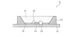
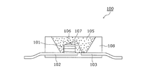
- FIG. 13 is a cross-sectional view showing a conventional semiconductor light emitting device disclosed in Patent Document 1.
- FIG. 13 is a cross-sectional view showing a conventional semiconductor light emitting device disclosed in Patent Document 1.
- a conventional semiconductor light emitting device 100 includes a semiconductor light emitting element 101 that emits ultraviolet light, blue light, or green light disposed in a container 108 in which electrical terminals 102 and 103 are embedded.
- a material 105 (cast epoxy resin layer) containing luminescent material particles 106 (inorganic luminescent material pigment) covers the inside of the container 108 so as to fill the semiconductor light emitting device 101.
- the electrode of the semiconductor light emitting element 101 is electrically connected to the electrical terminal 103 by a gold wire 107.
- a white LED light source is generally a combination of a blue LED and a green phosphor or a yellow phosphor, and a phosphor with excellent light emission characteristics and energy conversion efficiency is required to achieve high efficiency and high color rendering.
- Common phosphors used in white LEDs are fine crystal particles using rare earth ions as an activator, and many are chemically stable.
- quantum dot phosphors fine particles with a diameter of several nanometers to several tens of nanometers called quantum dot phosphors. It is expected as a new phosphor material containing no rare earth.
- the quantum dot phosphor can obtain a fluorescence spectrum in a desired wavelength band in the visible light region by controlling the particle diameter even with fine particles of the same material by the quantum size effect.
- it is light absorption and fluorescence by a band edge, since it shows a high external quantum efficiency of about 90%, a white LED having high efficiency and high color rendering can be provided.
- the quantum dot phosphor has a small particle size, the proportion of atoms occupying the surface of the fine particles increases, so many of them have low chemical stability, especially in excitation fluorescence in a high temperature environment.
- a major problem was that the photo-oxidation reaction on the phosphor surface progressed, causing a rapid decrease in luminous efficiency.
- the container containing the resin layer containing the quantum dot phosphor is configured like the container 108 described in Patent Document 1, and the heat of the cast epoxy resin layer is Because the conductivity is small, the resin layer becomes hot due to heat generation due to the Stokes loss of the quantum dot phosphor in the region away from the heat sink package and the frame resin layer, resulting in deterioration of the quantum dot phosphor and lowering the luminous efficiency. There is a problem.
- the present invention has been made to solve such a problem, and a highly reliable semiconductor light emitting device capable of suppressing a temperature rise of semiconductor fine particles such as a quantum dot phosphor and suppressing a decrease in light emission efficiency.
- the purpose is to provide.
- a first semiconductor light emitting device includes a package made of a resin having a recess, a lead frame exposed on the bottom surface of the recess, and a semiconductor installed on the lead frame in the recess.
- the first resin layer includes semiconductor fine particles having an excitation fluorescence spectrum that changes according to the particle diameter, and the first resin layer is made of a water-soluble or water-dispersible material.
- the semiconductor fine particles can be emulsified with the first resin layer, and the first resin layer containing the semiconductor fine particles can be formed with high density and high uniformity. Furthermore, since the first resin layer can be formed on the exposed lead frame, the heat dissipation of the first resin layer can be improved. As a result, the temperature rise of the semiconductor fine particles can be suppressed to prevent a decrease in the light emission efficiency, so that a semiconductor light emitting device with high efficiency, high color rendering properties and high reliability can be provided.
- the first semiconductor light emitting device further includes a metal reflection film formed on the side surface and the bottom surface of the recess, and the first resin layer is formed so as to cover the metal reflection film. preferable.
- the heat dissipation of the first resin layer can be further improved, and a more reliable semiconductor light emitting device can be provided.
- the semiconductor fine particles have a layer structure of two or more layers, and the outermost layer is a hydrophobic layer.
- the semiconductor fine particles are easily trapped in the main chain skeleton of the water-soluble resin by the hydrophobic interaction, so that the semiconductor fine particles can be dispersed and held in the first resin layer with higher density and higher uniformity. Thereby, it is possible to provide a semiconductor light emitting device with high efficiency and high color rendering without light unevenness.
- the first resin layer is preferably one of an acrylic resin, an epoxy resin, or a fluorine resin.
- the first resin layer has oxygen resistance and moisture resistance, a highly efficient and high color rendering semiconductor light emitting device can be provided.
- the second resin layer may be configured to include light scattering particles that scatter visible light.
- the light emitted from the semiconductor light emitting element is scattered back by the second resin layer, and more uniformly irradiated to the first resin layer in the package. Thereby, it is possible to provide a highly efficient and high color rendering semiconductor light emitting device free from light unevenness.
- the light scattering particles are white fine particles that reflect visible light, and the white fine particles preferably have a particle diameter of 100 nm or more.
- the light scattering particles have a particle diameter of 100 nm or more, include a wavelength at which the semiconductor fine particles absorb a part of light emitted by the semiconductor light emitting element. Phosphor fine particles that give an emission spectrum are preferred.
- the light scattering particles convert a part of the light of the semiconductor light emitting element to the longer wavelength side, so that the Stokes loss of the semiconductor fine particles is reduced and the temperature rise can be suppressed. Thereby, a highly efficient and high color rendering semiconductor light emitting device having high reliability can be provided.
- the semiconductor light emitting element emits blue light
- the semiconductor fine particles have red fluorescence
- the light scattering particles are rare earth phosphors having green fluorescence. can do.
- a second semiconductor light emitting device includes a semiconductor light emitting element mounted on a package having a conductive region and a phosphor layer provided in contact with the conductive region. It is composed of semiconductor fine particles having an excitation fluorescence spectrum that changes depending on the diameter, and a transparent resin that disperses and holds the semiconductor fine particles, and the transparent resin is a water-soluble or water-dispersible material. It is produced from a mixed solution of
- the semiconductor fine particles have a layer structure of two or more layers, and the outermost layer is a hydrophobic layer.
- the semiconductor fine particles are easily trapped by the hydrophobic chain in the main chain skeleton of the water-soluble resin, the semiconductor fine particles can be dispersed and held in the transparent resin with high density and high uniformity. Thereby, it is possible to provide a semiconductor light emitting device with high efficiency and high color rendering without light unevenness.
- the phosphor layer is preferably formed by an electrodeposition process.
- the semiconductor fine particles in which the ionic resin is dispersed in the solution can be electrophoresed on the substrate, and the semiconductor fine particles can be dispersed and held in the transparent resin with high density and high uniformity.
- the transparent resin containing the semiconductor fine particles is preferably any one of an acrylic resin, an epoxy resin, and a fluorine resin.
- semiconductor fine particles can be dispersed and contained in a transparent resin having oxygen resistance and moisture resistance. Thereby, a highly efficient and high color rendering semiconductor light emitting device can be provided.
- a light scattering layer is provided on the phosphor layer and the semiconductor light emitting element, and the light scattering layer includes light scattering particles and light scattering particles that scatter visible light. It is preferably composed of a transparent resin that is dispersed and held.
- the light emitted from the semiconductor light emitting element is scattered back by the light scattering layer, and is uniformly irradiated to the phosphor layer provided in the package.
- the light scattering fine particles contained in the light scattering layer are white fine particles that reflect visible light, and preferably have a particle diameter of 100 nm or more.
- the light scattering particles have a particle diameter of 100 nm or more, absorb part of the light emitted from the semiconductor light emitting element, and are included in the phosphor layer. It is preferable that the phosphor fine particles give an emission spectrum including a wavelength to be absorbed.
- the semiconductor light emitting element emits blue light
- the phosphor layer is a semiconductor fine particle having red fluorescence
- the light scattering particle is a rare earth phosphor having green fluorescence. Can be configured.
- a second method for manufacturing a semiconductor light emitting device wherein a metal reflective film is formed on an inner wall of a package having a conductive region except for at least a portion where a semiconductor light emitting element and a wire are connected.
- a phosphor layer is formed on the metal reflective film by an electrodeposition process while maintaining electrical insulation between the electrodes, and a light scattering layer is formed on the phosphor layer.
- the phosphor layer is in contact with the metal reflective film having a good thermal conductivity in a large area, the temperature rise of the phosphor layer can be suppressed. Thereby, it is possible to manufacture a semiconductor light emitting device having high reliability, high efficiency and high color rendering.
- the present invention since the temperature rise of the semiconductor fluorescent fine particles (quantum dot phosphor) can be suppressed, a semiconductor light emitting device having high reliability, high efficiency, and high color rendering can be provided.
- FIG. 1 is a schematic cross-sectional view of a semiconductor light-emitting device according to Embodiment 1 of the present invention.
- FIG. 2 is a schematic view showing a water-solubilization process of the epoxy resin used in the semiconductor light emitting device according to Embodiment 1 of the present invention.
- FIG. 3 is a schematic diagram showing how the quantum dot phosphor according to the present invention is captured by a resin.
- FIG. 4 is a schematic cross-sectional view of the quantum dot phosphor in the semiconductor light emitting device according to Embodiment 2 of the present invention.
- FIG. 5 is a schematic cross-sectional view of a semiconductor light emitting device according to Embodiment 3 of the present invention.
- FIG. 6 is a schematic diagram for explaining an electrodeposition process in the semiconductor light emitting device according to Embodiment 3 of the present invention.
- FIG. 7A is a cross-sectional view of the light reflecting resin layer forming step in the method for manufacturing a semiconductor light emitting device according to Embodiment 3 of the present invention.
- FIG. 7B is a cross-sectional view of the phosphor layer forming step in the method for manufacturing a semiconductor light emitting device according to Embodiment 3 of the present invention.
- FIG. 7C is a cross-sectional view of the semiconductor light-emitting element mounting step in the method for manufacturing a semiconductor light-emitting device according to Embodiment 3 of the present invention.
- FIG. 7A is a cross-sectional view of the light reflecting resin layer forming step in the method for manufacturing a semiconductor light emitting device according to Embodiment 3 of the present invention.
- FIG. 7B is a cross-sectional view of the phosphor layer forming step in the method for manufacturing
- FIG. 7D is a cross-sectional view of the wire bonding step in the method for manufacturing a semiconductor light emitting device according to Embodiment 3 of the present invention.
- FIG. 8A is a cross-sectional view of the semiconductor light-emitting element mounting step in the method for manufacturing a semiconductor light-emitting device according to Embodiment 4 of the present invention.
- FIG. 8B is a cross-sectional view of the phosphor layer forming step in the method for manufacturing a semiconductor light emitting device according to Embodiment 4 of the present invention.
- FIG. 8C is a cross-sectional view of the insulating protective film removing step in the method for manufacturing a semiconductor light emitting device according to Embodiment 4 of the present invention.
- FIG. 8A is a cross-sectional view of the semiconductor light-emitting element mounting step in the method for manufacturing a semiconductor light-emitting device according to Embodiment 4 of the present invention.
- FIG. 8B is a cross-sectional view of
- FIG. 9 is a schematic cross-sectional view of a semiconductor light-emitting device according to Embodiment 5 of the present invention.
- FIG. 10 is a schematic cross-sectional view of a semiconductor light emitting device according to a modification of the fifth embodiment of the present invention.
- FIG. 11 is a schematic cross-sectional view of a semiconductor light-emitting device according to Embodiment 8 of the present invention.
- FIG. 12 is a schematic cross-sectional view of a semiconductor light-emitting device according to Embodiment 9 of the present invention.
- FIG. 13 is a cross-sectional view of a conventional semiconductor light emitting device.
- FIG. 1 is a schematic cross-sectional view of a semiconductor light-emitting device according to Embodiment 1 of the present invention.
- a lead frame type package is used as the package.
- the semiconductor light emitting device 1 according to Embodiment 1 is a white LED light source that emits white light.
- the semiconductor light emitting device 1 includes a package (container) having a recess made of light reflecting resin layers 12 and 13, a lead frame 11 exposed on the bottom surface of the recess, and a lead frame 11 in the recess.
- the semiconductor light-emitting element 14 installed in the substrate, the phosphor layer 15 (first resin layer) formed so as to cover the bottom surface in the recess, and the resin formed on the phosphor layer 15 and the semiconductor light-emitting element 14.
- a layer 17 (second resin layer).
- the semiconductor light emitting element 14 in the present embodiment is an LED made of a bare chip, and is mounted in a predetermined area on the lead frame 11.
- the P electrode and the N electrode of the semiconductor light emitting element 14 are in electrical contact with the lead frame 11 by a gold wire 16.
- the phosphor layer 15 is formed on the exposed lead frame 11 in the package. That is, the phosphor layer 15 is formed so as to be in contact with the conductive region that becomes the heat sink of the lead frame 11. Thereby, the heat dissipation of the phosphor layer 15 can be improved.
- the phosphor layer 15 is formed outside the contact area of the gold wire 16 and the area where the semiconductor light emitting element 14 is mounted.
- the phosphor layer 15 in the present embodiment is formed not only on the bottom surface of the recess of the package but also on the side surface of the recess (the inner surface of the light reflecting resin layer 13) so as to coat the inner surface of the recess of the package. Are formed with substantially the same film thickness.
- the cup-shaped package is constituted by the lead frame 11 and the light reflecting resin layer 13.
- the resin layer 17 is made of a transparent resin and is filled in the package as a sealing resin.
- the resin layer 17 in this Embodiment is comprised only with transparent resin.
- the phosphor layer 15 is made of a water-soluble or water-dispersible resin material and a quantum dot phosphor. Specifically, the phosphor layer 15 has a configuration in which quantum dot phosphors are uniformly dispersed in a transparent resin having oxygen barrier properties and moisture resistance.
- an epoxy resin is used as the transparent resin for the phosphor layer 15.
- Epoxy resin is a material having oxygen permeability of 2 to 3 digits lower than that of silicone resin, and is one of resins that can be easily water-soluble or water-dispersible by amination. Further, as the transparent resin for the phosphor layer 15, a resin other than the epoxy resin can be used.
- a transparent resin made of a fluorine resin or an acrylic resin also has a high oxygen barrier property and a high moisture resistance.
- a material having oxygen barrier properties and moisture resistance as the transparent resin of the phosphor layer 15, it is possible to effectively suppress the photooxidation reaction of the quantum dot phosphor.
- semiconductor fine particles having an excitation fluorescence spectrum that varies depending on the particle diameter can be used as the quantum dot phosphor. In the quantum dot phosphor, the excitation fluorescence spectrum changes according to the particle diameter, and the emission wavelength of the quantum dot phosphor can be adjusted by changing the particle diameter.
- Preparation of the phosphor layer 15 according to the present invention includes a dispersion step of dispersing the quantum dot phosphor (phosphor fine particles) in a resin solution and a resin formation step. A description will be given below for each process.
- the phosphor layer 15 according to the present invention is formed of a water-soluble or water-dispersible resin solvent.
- a water-soluble resin has an ionized or electrically polar part of the resin molecular skeleton in an aqueous solution, and the polar part and ionized region of the resin molecule are stabilized by hydration, so it is dissolved or dispersed in water to become an emulsion. can do.
- FIG. 2 is a diagram showing a water-solubilization process of the epoxy resin used in the present embodiment. As shown in FIG. 2, it can ionize by aminating the terminal of an epoxy resin and neutralizing with an acid. In this embodiment, acetic acid is used as the acid to be neutralized.
- FIG. 3 is a diagram showing the capture of the quantum dot phosphor by a resin.
- a quantum dot phosphor 21 by adding a quantum dot phosphor 21 to a resin solution 20 neutralized with acetic acid 25, the main chain 23 of the epoxy resin solvent molecules having an aminated cation portion 22 becomes a quantum dot phosphor 24. To capture. Thereby, the quantum dot phosphor 21 can be uniformly dispersed in the resin solution 20.
- the particle size of the phosphor fine particles is large, the phosphor fine particles are not sufficiently trapped in the main chain of the resin solvent molecules and settle or settle in the resin solution 20.
- the particle diameter of commercially available rare earth phosphors is 1 ⁇ m to 100 ⁇ m, which is much larger than the size of resin solvent molecules. Therefore, many resin molecules are required to capture one rare-earth phosphor fine particle, and the dispersion concentration decreases or the sedimentation phenomenon occurs in the water-soluble resin, resulting in uneven brightness and light emission. End up.
- the particle diameter of the quantum dot phosphor is about 1 nm to 20 nm and the size is equal to or smaller than that of the water-soluble resin molecule, it can be dispersed uniformly and at a high concentration in the resin solution.
- the semiconductor fine particles used in the present embodiment are quantum dot phosphors having a diameter of about 1 nm to 10 nm with InP as a nucleus.
- any phosphor material may be used as long as it does not dissolve in water.
- Known cadmium quantum dot phosphors and chalcogenide fine particles may be used.
- a spray method (spray method) is used for the resin coating process.
- the spraying method is a method in which a resin solvent that captures fine particles is applied to an object by spraying a mist, and a resin coating can be formed on any object that has good wettability. Is possible.
- the lead frame type package has a resin region and a metal region.
- the package surface is made hydrophilic by plasma treatment using a mixed gas of Ar and H 2 or a mixed gas of Ar and O 2 . did.
- the resin is cured by spraying a resin solvent containing the quantum dot phosphor on the lead frame 11 in the form of a mist to heat the resin.
- the phosphor layer 15 can be formed only at the locations.
- a resin layer 17 made of a transparent silicone resin is filled in the package.
- the resin layer 17 is intended to protect the semiconductor light emitting element 14 and the phosphor layer 15, but the structure for protecting the semiconductor light emitting element 14 and the phosphor layer 15 is not necessarily the resin layer 17.
- the resin layer 17 instead of filling the resin layer 17, it may be configured to be sealed with a transparent glass plate.
- the lead frame type package is used.
- a ceramic package or a metal package formed of ceramic may be used.
- the quantum dot phosphor and the resin material in the phosphor layer 15 can be emulsified, the quantum dot phosphor is densely and highly uniform in the phosphor layer 15. Can be dispersed. Furthermore, since the phosphor layer 15 can be formed on the exposed lead frame 11, the heat dissipation of the phosphor layer 15 can be improved. Thereby, since the temperature rise of the fluorescent substance layer 15 can be suppressed and the fall of luminous efficiency can be suppressed, a highly efficient, high color rendering property, and highly reliable semiconductor light-emitting device can be provided.
- quantum dot phosphors have a two-layer or three-layer structure called a core-shell structure for the purpose of improving luminous efficiency and reliability, but for efficient dispersion in water-soluble resin solvents.
- a core-shell structure for the purpose of improving luminous efficiency and reliability, but for efficient dispersion in water-soluble resin solvents.
- the chemical properties of the outermost layer of the quantum dot are important.
- the terminal of the resin skeleton is ionized or polar functionalized, but the molecular skeleton is composed of hydrocarbons such as an alkyl main chain and is almost polar. Does not have. This means that the interaction with water is small and behaves as a hydrophobic group.
- the quantum dot phosphor to be trapped in the main chain of the water-soluble resin, the outermost layer of the quantum dot is nonpolar or polar. It is necessary to be composed of a weak ligand or layer. With this configuration, the quantum dot phosphor is easily trapped in the resin main chain by hydrophobic interaction, and thus can be emulsified and uniformly dispersed in the resin aqueous solution.
- FIG. 4 is a cross-sectional configuration diagram of the quantum dot phosphor in the semiconductor light emitting device according to Embodiment 2 of the present invention.
- FIG. 4 since it is the same as that of Embodiment 1 about components other than the structure of quantum dot fluorescent substance, detailed description is abbreviate
- the quantum dot phosphor used in the second embodiment has a three-layer structure, and a core 29 made of InP and a shell layer 30 made of ZnS formed so as to cover the outside of the core 29. And have. Further, as an outermost layer, a ligand layer 31 in which octane hydrocarbon is bonded as a ligand is provided outside the shell layer 30. Thus, the ligand layer 31 made of hydrocarbon is provided as the hydrophobic layer having strong hydrophobicity in the outermost layer, so that the quantum dot phosphor is efficiently trapped in the main chain of the resin molecule in the aqueous solution. .
- the quantum dot phosphor can be emulsified with high concentration and high uniformity.
- the quantum dot phosphor can be dispersed in the resin solution with higher density and higher uniformity, so that a highly efficient and high color rendering semiconductor light emitting device free from light unevenness can be provided.
- the quantum dot phosphor Since the quantum dot phosphor has a small core diameter, it has a core-shell layer-ligand layer multilayer structure of about 10 nm to 100 nm, and the size of the quantum dot phosphor is dispersed in the resin solution. Will not be affected. For this reason, the shell layer 30 and the ligand layer 31 are not particularly limited as long as the material structure is not decomposed by water. Since the ligand layer 31 preferably has a large hydrophobic interaction with the resin solution, a molecule having an alkyl main chain is preferable. On the other hand, in order to improve the dispersibility in the resin solution, a smaller molecular weight is preferable. Specifically, since it is necessary to be able to exist as a liquid at room temperature, the number of carbon atoms is preferably 15 or less.
- the quantum dot phosphor is a phosphor having a feature that the fluorescence wavelength varies with the particle diameter. Therefore, when the semiconductor light emitting element 14 emits blue light, in order to produce the phosphor layer 15 (phosphor film) that gives white fluorescence, a quantum dot phosphor having a particle diameter that gives red fluorescence and green fluorescence. What is necessary is just to produce the fluorescent substance layer containing both of the quantum dot fluorescent substance which has a particle diameter which gives.
- the particle diameter of the InP-based quantum dot phosphor according to the present embodiment is about 5 nm to 8 nm in the case of the green phosphor, and the largest particle diameter is about 10 nm to 20 nm in the case of the red fluorescence. Therefore, in the case of quantum dot phosphors, both red phosphors, green phosphors, and smaller blue phosphors, from the viewpoint of particle size, all quantum dot phosphors that fluoresce in the visible light region are exposed to the resin solution. Dispersion is possible. Therefore, a desired luminescent color can be obtained by mixing quantum dot phosphors having a plurality of particle sizes (different fluorescence wavelengths) in a resin solution.
- FIG. 5 is a schematic cross-sectional view of a semiconductor light emitting device according to Embodiment 3 of the present invention.
- the semiconductor light emitting device 3 is configured by the lead frame 11 and the light reflecting resin layers 12 and 13 as in the first embodiment.
- a semiconductor light emitting element 14 is mounted on the lead frame 11, and the P electrode and the N electrode of the semiconductor light emitting element 14 are electrically connected to the lead frame 11 by a gold wire 16.
- Embodiment 1 is different from Embodiment 1 in the configuration of the phosphor layer 15.
- the phosphor layer 15 in the present embodiment is formed only at the bottom of the recess of the package. That is, the phosphor layer 15 is provided on the conductive region that becomes the heat sink of the package, except for the contact region of the gold wire 16 and the region where the semiconductor light emitting element 14 is mounted. Accordingly, the phosphor layer 15 is formed only on the lowermost part on the inner side surface of the light reflecting resin layer 13, and the phosphor layer 15 is not formed on most of the inclined surface.
- the cup-shaped package made up of the lead frame 11 and the light reflecting resin layer 13 is filled with a resin layer 17 made of a transparent resin as in the first embodiment.
- the semiconductor light emitting device 3 was manufactured using an electrodeposition method as a method of forming a resin layer (phosphor layer 15) from a resin solution.
- the electrodeposition method is a method in which a voltage is applied to an object immersed in a resin solution, and an ionic resin solvent that captures the quantum dot phosphor is formed on the surface of the object by electrophoresis and electrochemical reaction. .
- the electrodeposition method since a film is formed by an electrochemical reaction, it is possible to form a resin layer with a uniform film thickness, and a uniform film can be formed even if the object to be coated has a complicated surface shape.
- the principle is an electrochemical reaction, a resin layer cannot be formed by an electrodeposition method unless it is a conductive object.
- the phosphor layer 15 was formed using a cationic electrodeposition method.
- FIG. 6 is a schematic view of the electrodeposition process.
- the epoxy resin is aminated (cationized), and an electrodeposition film is formed on the conductive region of the lead frame by using the lead frame as the cathode electrode 42.
- the resin solvent is an acid solvent
- the object to be coated becomes an anode, which is an anionic electrodeposition method.
- the resin coating film obtained by these methods is finally formed through a drying process and a curing process.
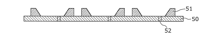
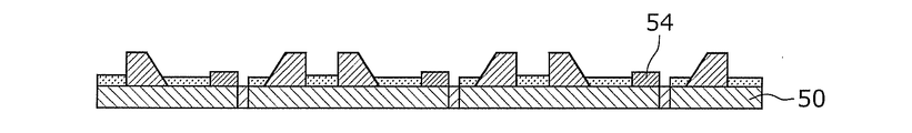
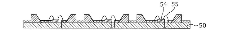
- FIGS. 7A to 7D are diagrams showing a part of a process cross-sectional view in the method for manufacturing a semiconductor light emitting device according to the third embodiment.
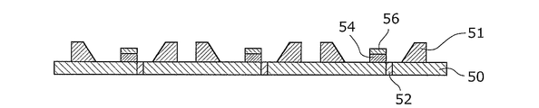
- light reflecting resin layers 51 and 52 are formed on the lead frame 50.
- a resist for insulation protection is applied in advance to the mounting region of the semiconductor light emitting element 14 and the contact region with the gold wire 16 on the lead frame 50, and the electrodeposition process shown in FIG.
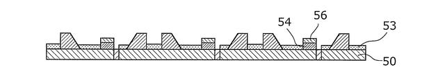
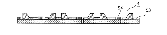
- the phosphor layer 53 containing the quantum dot phosphor is formed on the conductive region of the lead frame 50.
- the phosphor layer 53 is not electrodeposited on the light reflecting resin layers 51 and 52. Thereafter, after removing the resist, drying and thermosetting are performed.
- the semiconductor light emitting device 54 is mounted in a predetermined region on the lead frame 50, and as shown in FIG. 7D, the electrodes of the semiconductor light emitting device 54 and the electrode terminals of the lead frame 50 are formed by the gold wires 55. (Not shown) is electrically connected (wire bonding).
- the quantum dot phosphor in which the ionic resin is dispersed in the solution is electrophoresed on the lead frame.
- the quantum dot phosphor can be dispersed and held in the transparent resin with high density and high uniformity. Thereby, it is possible to provide a semiconductor light emitting device with high efficiency and high color rendering without light unevenness.
- the phosphor layer can be formed by electrodeposition bath after the semiconductor light emitting element is mounted and the wire is connected.
- the electrodeposition bath is immersed in a state where a potential difference is generated between the P electrode side and the N electrode side, an electrochemical reaction occurs due to the potential difference between the electrodes, and migration or dissolution of the electrode material occurs. Therefore, it is preferable to short-circuit the P side (P electrode) and the N side (N electrode) of the semiconductor light emitting element so that all the conductive regions have the same potential.
- the resin layer (phosphor layer 15) is preferably formed after the semiconductor light emitting element 14 is mounted.
- the semiconductor light-emitting element 54 is mounted on the lead frame 50 in a state where it is covered with an insulating protective film 56 such as a heat-resistant resist in advance.
- the resin layer (phosphor layer 53) containing the quantum dot phosphor is formed. This will be specifically described below.
- a resist as an insulating protective film 56 is applied by spin coating on the wafer before the semiconductor light emitting element 54 is separated into chips.
- the insulating protective film 56 is formed on the upper electrode of the semiconductor light emitting element 54.
- the semiconductor light emitting element 54 in which the insulating protective film 56 is formed is mounted on the lead frame 50 in which the light reflecting resin layers 51 and 52 are formed.
- the lead frame 50 in the state shown in FIG. 8A is immersed in an electrodeposition bath, so that quantum dot fluorescence is formed on the conductive region of the lead frame 50 as shown in FIG. 8B.
- the phosphor layer 53 containing the body can be formed.
- the phosphor layer 53 is not electrodeposited.
- the semiconductor light emitting device 4 having a structure in which only the upper portion of the semiconductor light emitting element 54 is not electrodeposited by the phosphor layer 53 can be realized. it can.
- the phosphor layer including the quantum dot phosphor can be formed only on the package and not in contact with the semiconductor light emitting element that becomes high temperature. Thereby, a highly reliable and high color rendering semiconductor light emitting device can be provided.
- a semiconductor light emitting device having the same configuration as that of the semiconductor light emitting device 3 according to the third embodiment shown in FIG. 5 can be manufactured.
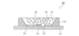
- FIG. 9 shows a schematic cross-sectional view of a semiconductor light emitting device according to Embodiment 5 of the present invention.
- the semiconductor light emitting device 5 according to the fifth embodiment includes light scattering particles 18 that scatter visible light in the resin layer 17 in the semiconductor light emitting device 1 according to the first embodiment shown in FIG. Is a structure in which is dispersed.
- white light particles made of titanium dioxide (TiO 2 ) that reflect visible light are used as the light scattering particles 18.
- light scattering particles 18 such as TiO 2 fine particles are mixed in advance with a transparent resin such as a silicone resin, and after the phosphor layer 15 is spray-coated, the transparent resin is placed in the package. It can be produced by injection.
- FIG. 10 shows the configuration of the semiconductor light emitting device 5A when the phosphor layer 15 is formed by electrodeposition.
- FIG. 10 is a schematic cross-sectional view of a semiconductor light emitting device according to a modification of the fifth embodiment of the present invention.
- the electrodeposition method can also be prepared by injecting a silicone resin containing light scattering particles 18 such as TiO 2 fine particles into the package after forming the phosphor layer 15 as in the spraying method.
- a silicone resin containing light scattering particles 18 such as TiO 2 fine particles
- the thermosetting temperature of a silicone resin is about 150 degreeC, it is preferable to use resin with high heat resistance, such as an epoxy resin and a fluorine resin, as resin which comprises the fluorescent substance layer 15.
- FIG. 10 shows the configuration of the semiconductor light emitting device 5A when the phosphor layer 15 is formed by electrodeposition.
- FIG. 10 is a schematic cross-sectional view of a semiconductor light emitting device according to a modification of the fifth embodiment of the present invention.
- the semiconductor light emitting device since the light scattering particles 18 are dispersed in the resin layer 17, the light emitted from the semiconductor light emitting element 14 is scattered by the resin layer 17 and fluorescent.
- the body layer 15 is irradiated more uniformly. Thereby, it is possible to provide a highly efficient and high color rendering semiconductor light emitting device free from light unevenness.
- a silicone resin is used as the resin layer 17, but the resin constituting the resin layer 17 is transparent and is lower than the melting temperature or decomposition temperature of the resin forming the phosphor layer 15. If it is resin hardened
- TiO 2 fine particles are used as the light scattering particles 18, but fine particles made of other materials may be used as long as they are white fine particles.
- lead white carbonate called lead white (2PbCO 3 ⁇ Pb (OH) 2
- ZnO called zinc white
- the light scattering particles 18 are a material that does not absorb the emission wavelength of the semiconductor light emitting element 14 and the fluorescence wavelength of the quantum dot phosphor. In order to reflect light from the semiconductor light emitting element 14 more efficiently, it is desirable that the particle diameter of the light scattering particles 18 is as large as the wavelength of the light emitted from the semiconductor light emitting element 14.
- the constituent material of the light scattering particles 18 is transparent to the light emitted from the semiconductor light emitting element 14.
- the size (particle diameter) of the fine particles is about the wavelength of the semiconductor light emitting element 14, a light scattering phenomenon called Mie scattering occurs.
- a light scattering phenomenon called Mie scattering occurs.
- white particles made of a transparent material are scattered white.
- the particle diameter of the light scattering particles 18 needs to be about one-fourth to one wavelength of the wavelength of light emitted from the semiconductor light-emitting element 14. Accordingly, the visible light region of the white LED is 400 nm to 700 nm, and the light scattering particle 18 needs to strongly reflect the blue light having the shortest wavelength, so the particle diameter of the light scattering particle 18 is about 100 nm or more. It is preferable that
- the light scattering particles 18 are white fine particles that reflect visible light, and the white fine particles have a particle diameter of 100 nm or more. It will scatter light without absorbing light. Thereby, it is possible to provide a highly efficient and high color rendering semiconductor light emitting device free from light unevenness.
- the light scattering particles 18 of the resin layer 17 absorb light from the semiconductor light emitting element 14 and use the excitation light of the quantum dot phosphor as fluorescence.
- a light scattering phosphor made of a rare earth phosphor that radiates may also be used. That is, the light scattering particle 18 may be a phosphor that absorbs a part of the light emitted by the semiconductor light emitting element 14 and gives an emission spectrum including a wavelength that the quantum dot phosphor absorbs.
- the particle diameter of the light scattering particles 18 made of a phosphor is 100 nm or more.
- a YAG (yttrium, aluminum, garnet) phosphor that is a rare earth phosphor is used as the light scattering phosphor that is the light scattering particle 18.
- the resin layer of the phosphor layer 15 contained a red quantum dot phosphor that gives red fluorescence.
- a part of the blue light emitted by the semiconductor light emitting element 14 that emits blue light is absorbed by the YAG phosphor of the resin layer 17, and yellowish green Give fluorescence.
- the red quantum dot phosphor absorbs a part of the yellow-green light emission and gives red fluorescence.
- the light scattering particles 18 need not be limited to the YAG phosphor, and may be any phosphor that can absorb the blue light of the semiconductor light emitting element 14 and convert the wavelength.
- the fluorescence spectrum of the YAG phosphor extends to a long wavelength region of 700 nm or more with almost no visibility, and although the color rendering is improved by combining with the red quantum dot phosphor, the luminous efficiency (lm / W) hardly changes. .
- a phosphor such as a sialon (SiAlON) phosphor that has a fluorescence spectrum centered on green with high visibility and whose fluorescence spectrum does not spread on the long wavelength side of 700 nm or more has a luminous efficiency (lm / W) is higher than the YAG phosphor. Therefore, by using the SiAlON phosphor as the light scattering particles 18 and combining with the red quantum dot phosphor, white light having high color rendering properties and high luminous efficiency (lm / W) can be obtained.
- SiAlON sialon
- the quantum dot phosphor converts the wavelength from green to red, the Stokes loss is smaller than that from blue to red, and the calorific value of the quantum dot phosphor is reduced. That is, since the light scattering particle 18 converts part of the light of the semiconductor light emitting element 14 to the longer wavelength side, the Stokes loss of the quantum dot phosphor is reduced. Thereby, since the temperature rise of a quantum dot can further be suppressed, the highly reliable color rendering semiconductor light-emitting device which has high reliability can be provided.
- FIG. 11 is a schematic cross-sectional view of a semiconductor light-emitting device according to Embodiment 8 of the present invention.
- the phosphor layer 15 is formed on the highly reflective metal film in order to efficiently extract the fluorescence obtained from the phosphor layer 15 from the semiconductor light emitting device.
- a metallic reflective film 19 made of gloss Ag is formed on the lead frame 11 and the insulating resin layer 62 by electroless plating.
- the metal reflection film 19 is formed on the inner wall of the package having the conductive region of the lead frame 11 except for the portion where the semiconductor light emitting element 14 and the wire connection are made.
- the metal reflection film 19 must prevent the P electrode and the N electrode in the semiconductor light emitting element 14 from being short-circuited.
- a region where Ag is not plated is formed by protecting the insulating resin layer 61 with a resist or the like in advance, thereby ensuring the insulation of the device.
- the metal reflection film 19 is formed on the side surface and the bottom surface of the recess of the package.
- the phosphor layer 15 is formed on the surface of the metal reflection film 19 by electrodeposition using the metal reflection film 19 made of Ag plating as an electrode.
- the semiconductor light emitting device since the phosphor layer 15 is formed on the metal reflection film 19, the heat dissipation of the phosphor layer 15 can be further improved. Therefore, a highly reliable semiconductor light emitting device can be provided.
- the metal reflection film 19 can be formed also on the insulating resin layer 62. Therefore, the phosphor layer 15 can be easily formed on the inner side surface of the package by using the electrodeposition method using the metal reflective film 19 as an electrode. Moreover, since the metal reflective film 19 has higher thermal conductivity than the insulating resin layer 62, the heat dissipation of the phosphor layer 15 is improved, and the temperature rise of the quantum dot phosphor can be suppressed.
- the electrical insulation between the electrodes of the semiconductor light emitting element 14 is maintained on the surface of the metal reflective film 19 formed on the inner surface of the package.
- the phosphor layer 15 is formed by the electrodeposition method, the phosphor layer 15 comes into contact with the metal reflective film 19 having a good thermal conductivity in a large area. Thereby, since the temperature rise of the phosphor layer 15 can be effectively suppressed, it is possible to manufacture a semiconductor light emitting device having high reliability, high efficiency and high color rendering.
- FIG. 12 is a schematic cross-sectional view of a semiconductor light-emitting device according to Embodiment 9 of the present invention.
- the semiconductor light emitting element 14 is one of the highest temperature regions in the semiconductor light emitting device of the present invention.
- the thermal conductivity of the resin layer 17 is increased, and the heat of the semiconductor light emitting element 14 is transmitted to the phosphor layer 15 through the resin layer 17.
- the temperature of the phosphor layer 15 rises.
- the junction temperature may exceed 150 ° C., so that the deterioration of the phosphor layer 15 is accelerated.
- heat generated by the phosphor layer 15 during wavelength conversion is dissipated to the conductive region of the lead frame 11 and at the same time, heat from the semiconductor light emitting element 14 is not easily transmitted to the phosphor layer 15.
- the semiconductor light emitting element 14 is covered with a transparent resin layer 70 that does not contain ceramic fine particles.
- the transparent resin layer 70 is made of only a silicone resin, and is formed in a dome shape so as to cover the semiconductor light emitting element 14.
- the transparent resin layer 70 does not contain ceramic fine particles, the thermal conductivity of the transparent resin layer 70 is kept lower than the thermal conductivity of the resin layer 17, and the heat of the semiconductor light emitting element 14 is reduced. Conduction upward (resin layer 17 side) can be suppressed. As a result, most of the heat of the semiconductor light emitting element 14 is dissipated through the lead frame 11, so that the temperature rise of the phosphor layer 15 can be suppressed even when the semiconductor light emitting element 14 is in a high output operation. It becomes.
- the semiconductor light emitting device it is possible to achieve both heat dissipation of the phosphor layer 15 during wavelength conversion and heat shielding from the semiconductor light emitting element 14 to the phosphor layer 15. Therefore, the temperature rise of the phosphor layer 15 can be suppressed even in a high output operation. Thereby, a highly reliable semiconductor light emitting device can be provided.
- a metal reflection film 19 is vapor-deposited as a highly reflective metal film on the inner wall of a region (concave portion) surrounded by the insulating resin layer 62 formed on the lead frame 11, and a fluorescence containing a quantum dot phosphor on the metal reflection film 19.
- a body layer 15 is deposited.
- the semiconductor light emitting element 14 is mounted in a predetermined region on the lead frame 11, the semiconductor light emitting element 14 and the gold wire 16 are connected by wire bonding, and then a transparent resin made of silicone resin so as to cover the semiconductor light emitting element 14.
- Layer 70 is formed by coating. In this state, defoaming is performed once. And shaping
- the resin layer 17 is formed by injecting a silicone resin containing the light scattering particles 18 onto the phosphor layer 15 and the transparent resin layer 70 so as to fill the concave portion of the insulating resin layer 62.
- the semiconductor light emitting device 9 having the configuration as shown in FIG. 12 can be manufactured.
- the semiconductor light emitting element 14 and the lead frame 11 are connected by the gold wire 16 and the transparent resin layer 70 is formed before the phosphor layer 15 is deposited on the metal reflective film 19. Thereafter, the phosphor layer 15 may be formed.
- the semiconductor light emitting device according to the present invention has been described based on the embodiment, but the present invention is not limited to the above embodiment.
- the LED is exemplified as the semiconductor light emitting element 14, but a semiconductor light emitting element such as a semiconductor laser, an organic EL (Electro Luminescence), or an inorganic EL may be used.
- a semiconductor light emitting element such as a semiconductor laser, an organic EL (Electro Luminescence), or an inorganic EL may be used.
- the blue LED is used as the semiconductor light emitting element 14, but the present invention is not limited to this. Further, the combination of the emission color of the semiconductor light emitting element 14 and the fluorescence color of the quantum dot phosphor of the phosphor layer 15 is not limited to the above embodiment.
- white light may be emitted by a blue LED that emits blue light and yellow phosphor particles that are excited by blue light and emit yellow light.
- an ultraviolet LED that emits ultraviolet light having a shorter wavelength than a blue LED, and blue phosphor particles, green phosphor particles, and red fluorescence that are mainly excited by ultraviolet light to emit blue light, red light, and green light.
- the body particles may be configured to emit white light. Thereby, a semiconductor light emitting device with high color rendering can be realized.
- a semiconductor light emitting device with high reliability, high efficiency, and high color rendering can be realized, so that it is widely useful as a white LED light source for display devices, lighting devices, and the like.
Abstract
L'invention concerne un dispositif luminescent à semi-conducteurs (1) qui est équipé : d'un boîtier constitué de résine qui possède une partie en retrait; d'une grille de connexion (11) exposée sur la face fond de la partie en retrait; d'un élément luminescent à semi-conducteurs (14) placé sur la grille de connexion (11) située à l'intérieur de la partie en retrait; d'une couche de phosphore (15) formée de manière à couvrir la face fond à l'intérieur de la partie en retrait; et d'une couche de résine (17) formée sur la couche de phosphore (15) et l'élément luminescent à semi-conducteurs (14). La couche de phosphore (15) contient des microparticules semi-conductrices possédant un spectre de fluorescence d'excitation qui varie selon le diamètre des particules. En outre, la couche de phosphore (15) est constituée d'un matériau hydrosoluble ou hydrodispersable.
Priority Applications (3)
| Application Number | Priority Date | Filing Date | Title |
|---|---|---|---|
| JP2013506847A JPWO2012131792A1 (ja) | 2011-03-31 | 2011-06-30 | 半導体発光装置 |
| CN2011800685713A CN103403892A (zh) | 2011-03-31 | 2011-06-30 | 半导体发光装置 |
| US14/011,445 US8872213B2 (en) | 2011-03-31 | 2013-08-27 | Semiconductor light emitting device |
Applications Claiming Priority (2)
| Application Number | Priority Date | Filing Date | Title |
|---|---|---|---|
| JP2011079273 | 2011-03-31 | ||
| JP2011-079273 | 2011-03-31 |
Related Child Applications (1)
| Application Number | Title | Priority Date | Filing Date |
|---|---|---|---|
| US14/011,445 Continuation US8872213B2 (en) | 2011-03-31 | 2013-08-27 | Semiconductor light emitting device |
Publications (1)
| Publication Number | Publication Date |
|---|---|
| WO2012131792A1 true WO2012131792A1 (fr) | 2012-10-04 |
Family
ID=46929640
Family Applications (1)
| Application Number | Title | Priority Date | Filing Date |
|---|---|---|---|
| PCT/JP2011/003752 WO2012131792A1 (fr) | 2011-03-31 | 2011-06-30 | Dispositif luminescent à semi-conducteurs |
Country Status (4)
| Country | Link |
|---|---|
| US (1) | US8872213B2 (fr) |
| JP (1) | JPWO2012131792A1 (fr) |
| CN (1) | CN103403892A (fr) |
| WO (1) | WO2012131792A1 (fr) |
Cited By (8)
| Publication number | Priority date | Publication date | Assignee | Title |
|---|---|---|---|---|
| JP2014195046A (ja) * | 2013-02-28 | 2014-10-09 | Nichia Chem Ind Ltd | 発光装置及びそれを備える照明装置 |
| JPWO2015020205A1 (ja) * | 2013-08-09 | 2017-03-02 | 株式会社タムラ製作所 | 発光装置 |
| JP2017112174A (ja) * | 2015-12-15 | 2017-06-22 | シャープ株式会社 | ナノ粒子蛍光体素子及び発光素子 |
| JP2017110059A (ja) * | 2015-12-15 | 2017-06-22 | シャープ株式会社 | 発光装置または発光装置用蛍光体含有シート |
| JP2017138558A (ja) * | 2016-02-05 | 2017-08-10 | 大日本印刷株式会社 | 画像表示装置 |
| WO2018123103A1 (fr) * | 2016-12-28 | 2018-07-05 | Dic株式会社 | Composition d'encre, couche de conversion de lumière et filtre de couleur |
| KR101915366B1 (ko) | 2015-12-15 | 2018-11-05 | 샤프 가부시키가이샤 | 형광체 함유 입자 및 그것을 사용한 발광 장치, 형광체 함유 시트 |
| JP2020072121A (ja) * | 2018-10-29 | 2020-05-07 | 日亜化学工業株式会社 | 発光装置の製造方法 |
Families Citing this family (34)
| Publication number | Priority date | Publication date | Assignee | Title |
|---|---|---|---|---|
| JP5886584B2 (ja) | 2010-11-05 | 2016-03-16 | ローム株式会社 | 半導体発光装置 |
| JP2014056896A (ja) * | 2012-09-11 | 2014-03-27 | Ns Materials Kk | 半導体を利用した発光デバイス及びその製造方法 |
| US9955619B2 (en) * | 2013-02-27 | 2018-04-24 | Nichia Corporation | Light emitting device, light emitting element mounting method, and light emitting element mounter |
| US9269857B2 (en) * | 2013-10-22 | 2016-02-23 | National Applied Research Laboratories | Method and system for eliminating yellow ring occurring on white light emitting diode |
| US9660151B2 (en) * | 2014-05-21 | 2017-05-23 | Nichia Corporation | Method for manufacturing light emitting device |
| KR102188500B1 (ko) * | 2014-07-28 | 2020-12-09 | 삼성전자주식회사 | 발광다이오드 패키지 및 이를 이용한 조명장치 |
| KR102237112B1 (ko) * | 2014-07-30 | 2021-04-08 | 엘지이노텍 주식회사 | 발광 소자 및 이를 구비한 광원 모듈 |
| JP6387787B2 (ja) * | 2014-10-24 | 2018-09-12 | 日亜化学工業株式会社 | 発光装置、パッケージ及びそれらの製造方法 |
| DE102015103840A1 (de) | 2015-03-16 | 2016-09-22 | Osram Opto Semiconductors Gmbh | Elektromagnetische Strahlung emittierende Baugruppe |
| KR102360957B1 (ko) * | 2015-03-27 | 2022-02-11 | 삼성디스플레이 주식회사 | 발광 다이오드 패키지 |
| CN104793284A (zh) * | 2015-04-30 | 2015-07-22 | 武汉华星光电技术有限公司 | 导光板、背光模块及液晶显示器 |
| JP6590579B2 (ja) * | 2015-08-03 | 2019-10-16 | シチズン電子株式会社 | Led発光素子 |
| JP6237826B2 (ja) * | 2015-09-30 | 2017-11-29 | 日亜化学工業株式会社 | パッケージ及び発光装置、並びにそれらの製造方法 |
| CN105319774A (zh) * | 2015-11-16 | 2016-02-10 | 深圳市华星光电技术有限公司 | 使用量子点膜片的显示装置 |
| WO2017086053A1 (fr) * | 2015-11-20 | 2017-05-26 | シャープ株式会社 | Source de lumière inoffensive pour l'œil |
| US9966515B2 (en) * | 2015-12-26 | 2018-05-08 | Nichia Corporation | Light emitting device and method of manufacturing the light emitting device |
| US20170250332A1 (en) * | 2016-02-25 | 2017-08-31 | Thomas Paulos | Heat dissipation from circuits through quantom dot optics and led integration |
| JP6650511B2 (ja) * | 2016-03-31 | 2020-02-19 | シャープ株式会社 | アイセーフ光源、およびその製造方法 |
| CN106299084B (zh) * | 2016-08-30 | 2018-10-16 | 开发晶照明(厦门)有限公司 | Led封装结构 |
| KR20180053489A (ko) * | 2016-11-11 | 2018-05-23 | 삼성전자주식회사 | 발광 소자 패키지 |
| KR20180081647A (ko) * | 2017-01-06 | 2018-07-17 | 삼성전자주식회사 | 발광 패키지 |
| JP2018137321A (ja) * | 2017-02-21 | 2018-08-30 | シャープ株式会社 | 発光装置および画像表示装置 |
| CN107705713B (zh) * | 2017-10-13 | 2019-12-27 | 上海天马微电子有限公司 | 一种显示面板和显示装置 |
| US10672960B2 (en) * | 2017-10-19 | 2020-06-02 | Lumileds Llc | Light emitting device package with a coating layer |
| KR20200065074A (ko) * | 2017-10-19 | 2020-06-08 | 루미레즈 엘엘씨 | 발광 디바이스 패키지 |
| CN109841721B (zh) * | 2017-11-28 | 2023-05-02 | 首尔半导体股份有限公司 | 发光二极管封装体及其制造方法 |
| US10600811B2 (en) | 2018-04-20 | 2020-03-24 | Wuhan China Star Optoelectronics Technology Co., Ltd. | TFT array substrate and LCD |
| CN108682753B (zh) * | 2018-05-16 | 2020-04-07 | 深圳市华星光电技术有限公司 | Oled显示面板及其制作方法 |
| CN108615742A (zh) * | 2018-07-10 | 2018-10-02 | 南方科技大学 | 一种显示面板制作方法、显示面板及显示装置 |
| JP6940775B2 (ja) * | 2018-10-30 | 2021-09-29 | 日亜化学工業株式会社 | 発光装置の製造方法 |
| US11125395B2 (en) * | 2019-08-15 | 2021-09-21 | Luminii Llc | Lighting system providing combined directional and ambient light |
| KR20220065153A (ko) | 2020-11-12 | 2022-05-20 | 삼성전자주식회사 | 광원 모듈 및 이를 포함하는 모바일 기기 |
| CN112909213B (zh) * | 2021-01-25 | 2023-04-18 | 中国计量大学 | 一种电驱动量子点单光子源及其制备方法 |
| WO2023241864A1 (fr) * | 2022-06-13 | 2023-12-21 | Ams-Osram International Gmbh | Procédé de fabrication d'un dispositif semi-conducteur émettant un rayonnement et dispositif semi-conducteur émettant un rayonnement |
Citations (5)
| Publication number | Priority date | Publication date | Assignee | Title |
|---|---|---|---|---|
| JP2003017751A (ja) * | 2001-06-28 | 2003-01-17 | Toyoda Gosei Co Ltd | 発光ダイオード |
| WO2004000971A1 (fr) * | 2002-06-19 | 2003-12-31 | National Institute Of Advanced Industrial Science And Technology | Phosphore a tres fines particules de semi-conducteur et dispositif luminescent |
| JP2005327820A (ja) * | 2004-05-12 | 2005-11-24 | Matsushita Electric Works Ltd | 発光ダイオード用パッケージおよびそれを用いた発光装置およびその発光装置の製造方法 |
| JP2010126596A (ja) * | 2008-11-26 | 2010-06-10 | Showa Denko Kk | 液状硬化性樹脂組成物、ナノ粒子蛍光体を含む硬化樹脂の製造方法、発光装置の製造方法、発光装置及び照明装置 |
| JP2010232203A (ja) * | 2009-03-25 | 2010-10-14 | Toyoda Gosei Co Ltd | 発光装置及びその製造方法 |
Family Cites Families (22)
| Publication number | Priority date | Publication date | Assignee | Title |
|---|---|---|---|---|
| DE19638667C2 (de) | 1996-09-20 | 2001-05-17 | Osram Opto Semiconductors Gmbh | Mischfarbiges Licht abstrahlendes Halbleiterbauelement mit Lumineszenzkonversionselement |
| EP2267801B1 (fr) | 1996-06-26 | 2015-05-27 | OSRAM Opto Semiconductors GmbH | Puce à semi-conducteur luminescente et composant à semi-conducteur luminescent |
| WO2000017655A1 (fr) * | 1998-09-18 | 2000-03-30 | Massachusetts Institute Of Technology | Nanocristaux semiconducteurs fluorescents hydrosolubles |
| MY145695A (en) * | 2001-01-24 | 2012-03-30 | Nichia Corp | Light emitting diode, optical semiconductor device, epoxy resin composition suited for optical semiconductor device, and method for manufacturing the same |
| JP2005136006A (ja) * | 2003-10-28 | 2005-05-26 | Matsushita Electric Works Ltd | 発光装置及びそれを用いた演出装置 |
| WO2005067066A1 (fr) * | 2004-01-07 | 2005-07-21 | Matsushita Electric Industrial Co., Ltd. | Source lumineuse a dels |
| JP2006261292A (ja) * | 2005-03-16 | 2006-09-28 | Sumitomo Metal Electronics Devices Inc | 発光素子収納用パッケージ |
| JP2007116131A (ja) * | 2005-09-21 | 2007-05-10 | Sanyo Electric Co Ltd | Led発光装置 |
| JP2007103512A (ja) * | 2005-09-30 | 2007-04-19 | Kyocera Corp | 発光装置 |
| JP2007123390A (ja) * | 2005-10-26 | 2007-05-17 | Kyocera Corp | 発光装置 |
| JP2007157798A (ja) * | 2005-11-30 | 2007-06-21 | Kyocera Corp | 発光装置 |
| JP2008117976A (ja) | 2006-11-06 | 2008-05-22 | Stanley Electric Co Ltd | 電気泳動を用いた色変換発光体装置の製造方法 |
| US7504272B2 (en) | 2006-11-06 | 2009-03-17 | Stanley Electric Co., Ltd. | Method for producing color-converting light-emitting device using electrophoresis |
| JP5334088B2 (ja) * | 2007-01-15 | 2013-11-06 | フューチャー ライト リミテッド ライアビリティ カンパニー | 半導体発光装置 |
| JP4953846B2 (ja) | 2007-02-06 | 2012-06-13 | スタンレー電気株式会社 | 発光装置およびその製造方法 |
| US8641256B2 (en) * | 2007-11-06 | 2014-02-04 | Sanken Electric Co., Ltd. | Semiconductor light emitting device, composite light emitting device with arrangement of semiconductor light emitting devices, and planar light source using composite light emitting device |
| CN102017206A (zh) * | 2008-04-17 | 2011-04-13 | 株式会社东芝 | 白光发射设备、背光灯、液晶显示设备、以及照明设备 |
| JPWO2009148131A1 (ja) * | 2008-06-06 | 2011-11-04 | 住友ベークライト株式会社 | 波長変換組成物及び波長変換組成物からなる層を備えた光起電装置 |
| JP2009298946A (ja) * | 2008-06-13 | 2009-12-24 | Toda Kogyo Corp | Al−C−N−O系蛍光体及び該Al−C−N−O系蛍光体の製造法 |
| CN102217102B (zh) * | 2008-11-14 | 2015-07-15 | 三星电子株式会社 | 半导体发光器件 |
| KR101562022B1 (ko) * | 2009-02-02 | 2015-10-21 | 삼성디스플레이 주식회사 | 발광 다이오드 유닛, 이를 포함하는 표시 장치 및 발광 다이오드 유닛 제조 방법 |
| CN103443941A (zh) * | 2011-03-31 | 2013-12-11 | 松下电器产业株式会社 | 半导体发光装置 |
-
2011
- 2011-06-30 CN CN2011800685713A patent/CN103403892A/zh active Pending
- 2011-06-30 JP JP2013506847A patent/JPWO2012131792A1/ja not_active Ceased
- 2011-06-30 WO PCT/JP2011/003752 patent/WO2012131792A1/fr active Application Filing
-
2013
- 2013-08-27 US US14/011,445 patent/US8872213B2/en not_active Expired - Fee Related
Patent Citations (5)
| Publication number | Priority date | Publication date | Assignee | Title |
|---|---|---|---|---|
| JP2003017751A (ja) * | 2001-06-28 | 2003-01-17 | Toyoda Gosei Co Ltd | 発光ダイオード |
| WO2004000971A1 (fr) * | 2002-06-19 | 2003-12-31 | National Institute Of Advanced Industrial Science And Technology | Phosphore a tres fines particules de semi-conducteur et dispositif luminescent |
| JP2005327820A (ja) * | 2004-05-12 | 2005-11-24 | Matsushita Electric Works Ltd | 発光ダイオード用パッケージおよびそれを用いた発光装置およびその発光装置の製造方法 |
| JP2010126596A (ja) * | 2008-11-26 | 2010-06-10 | Showa Denko Kk | 液状硬化性樹脂組成物、ナノ粒子蛍光体を含む硬化樹脂の製造方法、発光装置の製造方法、発光装置及び照明装置 |
| JP2010232203A (ja) * | 2009-03-25 | 2010-10-14 | Toyoda Gosei Co Ltd | 発光装置及びその製造方法 |
Non-Patent Citations (1)
| Title |
|---|
| LEI YUN ET AL.: "Incorporating fluorescent quantum dots into water-soluble polymer", J LUMIN, vol. 128, no. 3, March 2008 (2008-03-01), pages 277 - 281 * |
Cited By (10)
| Publication number | Priority date | Publication date | Assignee | Title |
|---|---|---|---|---|
| JP2014195046A (ja) * | 2013-02-28 | 2014-10-09 | Nichia Chem Ind Ltd | 発光装置及びそれを備える照明装置 |
| JPWO2015020205A1 (ja) * | 2013-08-09 | 2017-03-02 | 株式会社タムラ製作所 | 発光装置 |
| US10340429B2 (en) | 2013-08-09 | 2019-07-02 | Koha Co., Ltd. | Light emitting device |
| JP2017112174A (ja) * | 2015-12-15 | 2017-06-22 | シャープ株式会社 | ナノ粒子蛍光体素子及び発光素子 |
| JP2017110059A (ja) * | 2015-12-15 | 2017-06-22 | シャープ株式会社 | 発光装置または発光装置用蛍光体含有シート |
| KR101915366B1 (ko) | 2015-12-15 | 2018-11-05 | 샤프 가부시키가이샤 | 형광체 함유 입자 및 그것을 사용한 발광 장치, 형광체 함유 시트 |
| JP2017138558A (ja) * | 2016-02-05 | 2017-08-10 | 大日本印刷株式会社 | 画像表示装置 |
| WO2018123103A1 (fr) * | 2016-12-28 | 2018-07-05 | Dic株式会社 | Composition d'encre, couche de conversion de lumière et filtre de couleur |
| JPWO2018123103A1 (ja) * | 2016-12-28 | 2018-12-27 | Dic株式会社 | インク組成物、光変換層及びカラーフィルタ |
| JP2020072121A (ja) * | 2018-10-29 | 2020-05-07 | 日亜化学工業株式会社 | 発光装置の製造方法 |
Also Published As
| Publication number | Publication date |
|---|---|
| US20130341666A1 (en) | 2013-12-26 |
| US8872213B2 (en) | 2014-10-28 |
| CN103403892A (zh) | 2013-11-20 |
| JPWO2012131792A1 (ja) | 2014-07-24 |
Similar Documents
| Publication | Publication Date | Title |
|---|---|---|
| WO2012131792A1 (fr) | Dispositif luminescent à semi-conducteurs | |
| JP4451178B2 (ja) | 発光デバイス | |
| WO2012132232A1 (fr) | Dispositif luminescent à semi-conducteurs | |
| KR100609830B1 (ko) | 녹색 및 적색형광체를 이용하는 백색 반도체 발광장치 | |
| JP4473284B2 (ja) | 発光装置およびその製造方法 | |
| KR100610249B1 (ko) | 황색 발광 형광체 및 그것을 채용한 백색 반도체 발광장치 | |
| JP5569389B2 (ja) | 発光装置の製造方法及び発光装置 | |
| WO2011111293A1 (fr) | Corps en résine pour l'encapsulation de diodes électroluminescentes, dispositif à diodes électroluminescentes, et procédé de fabrication de ce dispositif | |
| JP2008115223A (ja) | 蛍光体含有ガラスシート、その製造方法及び発光装置 | |
| JP2004055632A (ja) | 半導体発光装置 | |
| TW201705542A (zh) | 發光二極體裝置之製造方法及發光二極體元件 | |
| JP4266234B2 (ja) | 半導体発光装置の製造方法 | |
| JP5454154B2 (ja) | 発光装置および発光装置の製造方法 | |
| US20140312375A1 (en) | Method for producing an optoelectronic assembly and optoelectronic assembly | |
| JP4473285B2 (ja) | 発光装置およびその製造方法 | |
| JP2010251441A (ja) | 照明用ledモジュール | |
| JP2007235104A (ja) | 発光装置の製造方法および発光装置 | |
| KR101901890B1 (ko) | 발광 장치 | |
| JP2011009450A (ja) | 陽極酸化アルミナ膜の発光体及びその発光体を有する発光装置。 | |
| JP2002134790A (ja) | 半導体発光装置及びその製法 | |
| JP6803539B2 (ja) | 発光装置、及び、照明装置 | |
| US11456402B2 (en) | Light-emitting device and method of manufacturing the light-emitting device | |
| JP2008166311A (ja) | 半導体発光素子及び半導体発光装置 | |
| JPWO2018212300A1 (ja) | 発光装置 | |
| JP4473283B2 (ja) | 発光装置およびその製造方法 |
Legal Events
| Date | Code | Title | Description |
|---|---|---|---|
| 121 | Ep: the epo has been informed by wipo that ep was designated in this application |
Ref document number: 11861909 Country of ref document: EP Kind code of ref document: A1 |
|
| ENP | Entry into the national phase |
Ref document number: 2013506847 Country of ref document: JP Kind code of ref document: A |
|
| NENP | Non-entry into the national phase |
Ref country code: DE |
|
| 122 | Ep: pct application non-entry in european phase |
Ref document number: 11861909 Country of ref document: EP Kind code of ref document: A1 |