WO2012117974A1 - 発光装置 - Google Patents
発光装置 Download PDFInfo
- Publication number
- WO2012117974A1 WO2012117974A1 PCT/JP2012/054627 JP2012054627W WO2012117974A1 WO 2012117974 A1 WO2012117974 A1 WO 2012117974A1 JP 2012054627 W JP2012054627 W JP 2012054627W WO 2012117974 A1 WO2012117974 A1 WO 2012117974A1
- Authority
- WO
- WIPO (PCT)
- Prior art keywords
- light emitting
- resin
- emitting element
- lead frame
- emitting device
- Prior art date
- Legal status (The legal status is an assumption and is not a legal conclusion. Google has not performed a legal analysis and makes no representation as to the accuracy of the status listed.)
- Ceased
Links
Images




Classifications
-
- F—MECHANICAL ENGINEERING; LIGHTING; HEATING; WEAPONS; BLASTING
- F21—LIGHTING
- F21V—FUNCTIONAL FEATURES OR DETAILS OF LIGHTING DEVICES OR SYSTEMS THEREOF; STRUCTURAL COMBINATIONS OF LIGHTING DEVICES WITH OTHER ARTICLES, NOT OTHERWISE PROVIDED FOR
- F21V21/00—Supporting, suspending, or attaching arrangements for lighting devices; Hand grips
-
- H—ELECTRICITY
- H10—SEMICONDUCTOR DEVICES; ELECTRIC SOLID-STATE DEVICES NOT OTHERWISE PROVIDED FOR
- H10H—INORGANIC LIGHT-EMITTING SEMICONDUCTOR DEVICES HAVING POTENTIAL BARRIERS
- H10H20/00—Individual inorganic light-emitting semiconductor devices having potential barriers, e.g. light-emitting diodes [LED]
- H10H20/80—Constructional details
- H10H20/85—Packages
- H10H20/857—Interconnections, e.g. lead-frames, bond wires or solder balls
-
- H—ELECTRICITY
- H10—SEMICONDUCTOR DEVICES; ELECTRIC SOLID-STATE DEVICES NOT OTHERWISE PROVIDED FOR
- H10H—INORGANIC LIGHT-EMITTING SEMICONDUCTOR DEVICES HAVING POTENTIAL BARRIERS
- H10H20/00—Individual inorganic light-emitting semiconductor devices having potential barriers, e.g. light-emitting diodes [LED]
- H10H20/80—Constructional details
- H10H20/85—Packages
- H10H20/8506—Containers
-
- H—ELECTRICITY
- H10—SEMICONDUCTOR DEVICES; ELECTRIC SOLID-STATE DEVICES NOT OTHERWISE PROVIDED FOR
- H10H—INORGANIC LIGHT-EMITTING SEMICONDUCTOR DEVICES HAVING POTENTIAL BARRIERS
- H10H20/00—Individual inorganic light-emitting semiconductor devices having potential barriers, e.g. light-emitting diodes [LED]
- H10H20/80—Constructional details
- H10H20/85—Packages
- H10H20/855—Optical field-shaping means, e.g. lenses
- H10H20/856—Reflecting means
-
- H—ELECTRICITY
- H10—SEMICONDUCTOR DEVICES; ELECTRIC SOLID-STATE DEVICES NOT OTHERWISE PROVIDED FOR
- H10H—INORGANIC LIGHT-EMITTING SEMICONDUCTOR DEVICES HAVING POTENTIAL BARRIERS
- H10H20/00—Individual inorganic light-emitting semiconductor devices having potential barriers, e.g. light-emitting diodes [LED]
- H10H20/80—Constructional details
- H10H20/85—Packages
- H10H20/858—Means for heat extraction or cooling
- H10H20/8585—Means for heat extraction or cooling being an interconnection
-
- H—ELECTRICITY
- H10—SEMICONDUCTOR DEVICES; ELECTRIC SOLID-STATE DEVICES NOT OTHERWISE PROVIDED FOR
- H10W—GENERIC PACKAGES, INTERCONNECTIONS, CONNECTORS OR OTHER CONSTRUCTIONAL DETAILS OF DEVICES COVERED BY CLASS H10
- H10W72/00—Interconnections or connectors in packages
- H10W72/851—Dispositions of multiple connectors or interconnections
- H10W72/874—On different surfaces
- H10W72/884—Die-attach connectors and bond wires
-
- H—ELECTRICITY
- H10—SEMICONDUCTOR DEVICES; ELECTRIC SOLID-STATE DEVICES NOT OTHERWISE PROVIDED FOR
- H10W—GENERIC PACKAGES, INTERCONNECTIONS, CONNECTORS OR OTHER CONSTRUCTIONAL DETAILS OF DEVICES COVERED BY CLASS H10
- H10W74/00—Encapsulations, e.g. protective coatings
-
- H—ELECTRICITY
- H10—SEMICONDUCTOR DEVICES; ELECTRIC SOLID-STATE DEVICES NOT OTHERWISE PROVIDED FOR
- H10W—GENERIC PACKAGES, INTERCONNECTIONS, CONNECTORS OR OTHER CONSTRUCTIONAL DETAILS OF DEVICES COVERED BY CLASS H10
- H10W90/00—Package configurations
- H10W90/701—Package configurations characterised by the relative positions of pads or connectors relative to package parts
- H10W90/731—Package configurations characterised by the relative positions of pads or connectors relative to package parts of die-attach connectors
- H10W90/736—Package configurations characterised by the relative positions of pads or connectors relative to package parts of die-attach connectors between a chip and a stacked lead frame, conducting package substrate or heat sink
-
- H—ELECTRICITY
- H10—SEMICONDUCTOR DEVICES; ELECTRIC SOLID-STATE DEVICES NOT OTHERWISE PROVIDED FOR
- H10W—GENERIC PACKAGES, INTERCONNECTIONS, CONNECTORS OR OTHER CONSTRUCTIONAL DETAILS OF DEVICES COVERED BY CLASS H10
- H10W90/00—Package configurations
- H10W90/701—Package configurations characterised by the relative positions of pads or connectors relative to package parts
- H10W90/751—Package configurations characterised by the relative positions of pads or connectors relative to package parts of bond wires
- H10W90/756—Package configurations characterised by the relative positions of pads or connectors relative to package parts of bond wires between a chip and a stacked lead frame, conducting package substrate or heat sink
Definitions
- the present invention relates to a light emitting device used for various light sources including a lighting fixture, a display, a backlight of a mobile phone and a mobile terminal, and a moving image illumination auxiliary light source.
- a light-emitting device using a light-emitting element such as a light-emitting diode (LED) or a laser diode (LD) is small and has high light emission efficiency, and can emit clear light. Furthermore, it has excellent initial driving characteristics and excellent durability against vibration and repeated on / off. For this reason, light emitting devices having light emitting elements are used as various light sources.
- a side surface is formed of a resin or the like, and a bottom surface is provided with a lead frame made of metal together with a resin.
- a configuration in which a concave portion (cavity) is provided in a package or the like and a light emitting element is disposed on the lead frame in the concave portion is used.
- Patent Document 2 for example, refer to FIG. 3 of the same document
- a lead frame having a uniform thickness is bent and protrudes from the upper surface of the lead frame.
- a light emitting device in which a light emitting element is placed on the protruding portion and a light emitting device is placed on the protruding portion, and the upper surface of the lead frame is covered with resin except for the protruding portion and is not exposed from the bottom of the concave portion.
- the lead frame has a function as a heat sink that absorbs heat generated by the light emitting element and dissipates heat to the outside of the light emitting device. For this reason, if the lead frame is disposed only directly below the light emitting element, the volume of the lead frame is small, so that the heat generated by the light emitting element cannot be sufficiently absorbed. For this reason, since a larger lead frame is used, the surface of the wider lead frame, in particular, the portion where the light emitting element is not placed is exposed at the bottom surface of the recess (cavity).
- Resin can be easily obtained with a high reflectance such as 80% or more by appropriately selecting its type, color, and the like.
- the lead frame is made of a metal such as an iron alloy, a copper alloy containing phosphor bronze, or a nickel alloy, which has a problem that the reflectance is lower than that of the resin.
- the conventional light emitting device has a problem that it is difficult to further improve the power efficiency because the lead frame having a high light reflectance occupies a certain percentage or more of the area of the bottom surface of the recess provided in the package. It was.
- a method for improving the reflectivity of the lead frame a method of coating the lead frame with silver having a high reflectivity by plating or the like is known.
- silver corrodes in the air or in the resin with the passage of time, the surface is discolored and the reflectance is lowered, so that the coating by silver plating is often not a permanent measure.
- the present invention has high power efficiency by improving the reflectivity of the element mounting surface on which the light emitting element of the package is disposed, such as the bottom surface of the recess of the package in which the light emitting element is disposed, and generates heat of the light emitting element. It is an object to provide a light emitting device that can easily dissipate heat.
- Aspect 1 of the present invention includes a package including a resin portion, one or more lead frames disposed inside the resin portion, and a light emitting element electrically connected to at least one of the lead frames.
- the at least one of the lead frames has at least one convex portion on an upper surface, the side surface of the at least one convex portion is surrounded by the resin portion, and An upper surface of a certain convex portion is exposed from the resin portion, the light emitting element is placed on the upper surface of the convex portion, and at least half of the area of the upper surface of the convex portion is covered with the light emitting element. It is.
- the light emitting device includes at least one lead frame having at least one convex portion on the upper surface, as will be described in detail later.
- the at least one convex portion is exposed from the resin portion, and the light emitting element is mounted on the exposed convex portion via a eutectic alloy or paste having an adhesive action as necessary. And at least half of the area of the upper surface of the convex portion is covered with the light emitting element.
- the exposure of the lead frame having a low reflectance can be reduced, and a high reflectance can be obtained.
- the heat generated by the heat generation of the light emitting element can be spread over the entire lead frame through the convex portion directly under the light emitting element, and is thus easily absorbed by the lead frame and then released to the outside of the light emitting device.
- Aspect 2 of the present invention is the light emitting device according to aspect 1, wherein the area of the bottom surface of the light emitting element is 50% to 150% with respect to the area of the top surface of the convex portion.
- the vertical length and the horizontal length of the bottom surface of the light emitting element are within a range of plus or minus 0.1 mm with respect to the vertical length and the horizontal length of the top surface of the convex portion, respectively.
- Aspect 4 of the present invention is the light emitting device according to aspect 1 or 2, wherein the shape of the upper surface of the convex portion is a shape with rounded corners.
- Aspect 5 of the present invention is characterized in that an area of the upper surface of the convex portion is smaller than an area of the bottom surface of the light emitting element, and the light emitting element is mounted to the outside of the upper surface of the convex portion on the element mounting surface.
- the light-emitting device according to any one of Embodiments 1 to 4.
- Aspect 6 of the present invention is the light-emitting device according to any one of aspects 1 to 4, wherein the area of the top surface of the convex portion is the same as the area of the bottom surface of the light-emitting element.
- Aspect 7 of the present invention is the light emitting device according to any one of Aspects 1 to 6, wherein on the element mounting surface, the upper surface of the convex portion protrudes from the surface of the resin portion.
- a portion directly below the convex portion on which the light emitting element is placed is exposed from the resin portion. It is a light-emitting device as described in above.
- Aspect 9 of the present invention is the light emitting device according to any one of aspects 1 to 8, wherein the resin portion has a recess, and the element mounting surface is a bottom surface of the recess.
- Aspect 10 of the present invention is characterized in that the lead frame has at least two convex portions, and the resin of the resin portion is filled between the at least two convex portions. 9.
- the light emitting device according to any one of 9 above.
- a package including a resin portion, one or more lead frames arranged inside the resin portion, and electrically connected to at least one of the lead frames.
- a light emitting device including a light emitting device disposed on a mounting surface, wherein at least one of the lead frames has at least two convex portions on an upper surface, and the element is between the at least two convex portions.
- a resin for forming a mounting surface is included, and at least one of the convex portions has a top surface of the convex portion exposed from the resin portion on the element mounting surface, and the light emitting element is mounted on the top surface of the convex portion. This is a light-emitting device.
- the light emitting device includes at least one lead frame having at least two convex portions on the upper surface, as will be described in detail later.
- a resin that forms a part of the element mounting surface (for example, a recess of the package) of the package exists in the gap between the two protrusions.
- at least one of the convex portions is exposed from the resin portion on the element mounting surface on which the light emitting element is mounted, and on the exposed convex portions, a eutectic alloy having an adhesive action as necessary or The light emitting element is placed via the paste. Accordingly, one surface of the resin portion functions as a reflection surface that reflects light from the light emitting element.
- the resin enters the gap between the two convex portions, so that the exposure of the lead frame having a low reflectivity can be reduced and the high reflectivity can be obtained on the element mounting surface on which the light emitting element is arranged. Can do.
- the two convex portions are connected in the resin portion, the heat generated by the heat generation of the light emitting element can spread through the convex portion directly under the light emitting element to the entire lead frame including the other convex portion. Therefore, it is easily absorbed by the lead frame and then radiated outside the light emitting device.
- the resin portion has a recess
- the element mounting surface is a bottom surface of the recess
- a connection portion between the side surface of the recess and the bottom surface of the recess is the at least two protrusions. It is located in the upper part between, It is a light-emitting device of aspect 11 characterized by the above-mentioned.
- At least one of the lead frames has at least two convex portions having convex upper surfaces exposed from the resin portion on the element mounting surface, and the light emission is performed on one of the convex portions.
- 13 The light-emitting device according to aspect 11 or 12, wherein an element is placed, and a wire electrically connected to the light-emitting element is connected to the other.
- the light emitting device can improve the reflectance by easily suppressing the exposure of the lead frame on the element mounting surface of the package in which the light emitting elements are arranged, thereby obtaining high power efficiency. be able to. Furthermore, it is possible to easily dissipate heat generated by the light emitting element.
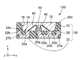
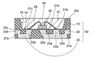
- FIG. 2 is a cross-sectional view showing a II-II cross section of FIG. 1.
- 3 is a plan view of a package 30 of the light emitting device 100.
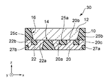
- FIG. FIG. 4 is a cross-sectional view showing a cross section IV-IV in FIG. 3.
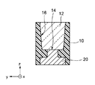
- FIG. 5 is a cross-sectional view showing a VV cross section of FIG. 3.
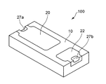
- 2 is a perspective view illustrating a bottom surface and a side surface of the light emitting device 100.
- FIG. It is sectional drawing which shows another embodiment of the positional relationship of the bottom face 14 of the recessed part 12 of the resin part 10, and a convex part upper surface.
- FIG. 8A is a plan view of a package 30A according to the first modification of the present invention
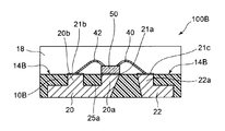
- FIG. 8B is a plan view of the light emitting device 100A according to the first modification of the present invention. It is sectional drawing of the light-emitting device 100B which concerns on the modification 2 of this invention.
- FIG. 10A is a process schematic diagram showing a first manufacturing method of the light emitting device 100 according to the present invention
- FIG. 10B shows a second manufacturing method of the light emitting device 100 according to the present invention.
- It is process schematic. 2 is a cross-sectional view showing more detailed shapes of a lead frame 20 and a lead frame 22 formed by etching.
- FIG. 1 is a plan view of a light emitting device 100 according to the present invention
- FIG. 2 is a cross-sectional view showing a II-II cross section of FIG. 3 is a plan view in which the light emitting element 50 and the wires 40 and 42 are omitted from the light emitting device 100 shown in FIG. 1 in order to facilitate understanding, that is, the plan view of the package 30 of the light emitting device 100.
- the figure is shown. 4 is a cross-sectional view showing a cross section taken along line IV-IV of FIG. 3
- FIG. 5 is a cross-sectional view showing a cross section taken along line VV of FIG.
- the package 30 includes a resin portion (package main body) 10 having a recess (cavity) 12 on the upper surface, and at least one lead frame that is located inside (at least immediately below) the recess 12 within the resin portion 10. have.
- the embodiment shown in FIGS. 1 and 3 has two lead frames 20 and 22.
- the light emitting device 100 further includes a light emitting element 50 disposed on the lead frame 20 inside the recess 12.
- the light emitting element 50 is electrically connected to at least one lead frame using a wire or the like as necessary.
- the light emitting element 50 is connected to the lead frame 20 by a wire 40.
- the wire 42 is connected to the lead frame 22.
- the recess 12 is preferably filled with a sealing material whose details will be described later as shown. The light emitting device 100 having such a configuration and effect will be described in detail below.
- the upper surface of the lead frame 20 disposed inside the resin portion 10 includes at least one (for example, a convex portion 20a whose details will be described later), preferably at least two convex portions.
- the embodiment shown in FIGS. 1 to 5 has three convex portions (for example, portions where the thickness in the z direction increases) 20a, 20b, and 20c.
- the convex portion 20 a and the convex portion 20 b are located below the bottom surface 14 of the concave portion 12 of the resin portion 10. That is, in the light emitting device 100, at least one of the convex portions is located below (directly below) the bottom surface 14 of the concave portion 12 of the resin portion 10.
- the upper surface (also referred to as “top surface”) of the convex portion 20 a is not covered with the resin of the resin portion 10, that is, is exposed from the resin portion 10 at the bottom surface 14 of the concave portion 12.
- the upper surface (top surface) of the convex portion 20b is also exposed from the bottom surface 14 of the resin portion 10 on the element mounting surface.
- the bottom surface 14 refers to the upper surface of the convex portion exposed from the resin portion 10 (the resin constituting the resin 10) in addition to the portion made of the resin constituting the resin portion 10 (in the embodiment of FIGS. 3 and 4).
- the bottom surface 14 corresponds to an element mounting surface on which the light emitting element 50 is disposed.
- the light emitting element 50 is placed on the upper surface of the convex portion 20a exposed from the bottom surface 14 of the resin portion 10 (that is, the upper surface of the convex portion 20a functions as a light emitting element mounting pattern).
- the light emitting element 50 may be fixed by using eutectic bonding using an Au—Sn alloy or the like, or a paste such as a silicon paste, a silver paste, or a resin paste.
- the protrusions 20a, 20b, and 20c preferably have a height (z direction in FIGS. 1 and 2) that is approximately half the thickness of the lead frame 20 or less.
- the height to the bottom surface 14 (the height of the convex portion of the frame 20 from the upper surface of the portion to the upper surface of the convex portion) is 0.2 mm or less, more preferably 0.01 mm to 0.1 mm. preferable.
- the vertical (x direction in FIGS. 1 and 2) and horizontal (y direction in FIGS. 1 and 2) of the upper surface are set so as to have an area sufficient for bonding the light emitting element 50 and the wire 40 placed on the upper surface. It is preferable to do.
- the area of the bottom surface of the light emitting element 50 is preferably 50% to 150% with respect to the area of the upper surface of the convex portion 20a. This makes it possible to achieve both good heat dissipation and good light-emitting element mounting properties.
- the area of the convex portion 20b to which the wire 40 is bonded may be substantially the same as or smaller than the area of the convex portion 20a on which the light emitting element 50 is placed.
- the distance between the convex parts 20a, 20b, and 20c, which are closest to each other depends on the processing method. For example, if etching is used, the distance is reduced to about 0.1 mm. can do. Preferably it is 0.1 mm or more.
- the light emitting element 50 may be electrically connected to the lead frame 20.
- One of the preferable connection forms is to connect the upper surface of the convex part 20b and the light emitting element 50 with a wire as shown in the figure (that is, the upper surface of the convex part 20b functions as a wire pattern).
- the light emitting element 50 may not be electrically connected to the lead frame 20.
- the lead frame 20 has only one convex portion (for example, the convex portion 20a) and the light emitting element 50 is placed on the upper surface of the only convex portion, the light emitting element 50 is a lead.
- the frame 20 may not be electrically connected.
- a gap (concave part) 25a between the convex part 20a and the convex part 20b of the lead frame 20 is filled with the resin of the resin part 10, and the resin present in the gap 25a is at the upper end of the gap 25a.
- a part of the bottom surface 14 of the recess 12 is formed.
- the gap 25b between the protrusion 20b and the protrusion 20c is also filled with the resin of the resin part 10, and the resin present in the gap 25b is also at the upper end of the gap 25b.
- a part of the bottom surface 14 of the recess 12 is formed.
- the lead frame 20 has at least two convex portions on the upper surface, there is a resin that forms the bottom surface 14 of the resin portion 10 in a gap formed between the at least two convex portions. . Furthermore, at least one of the convex portions on the upper surface of the lead frame 20 (the convex portion 20a) is exposed from the resin portion 10 on the bottom surface 14, and the light emitting element 50 is mounted on the upper surface of the exposed convex portion 20a.
- the resin is filled in the gap 25a and the gap 25b of the lead frame 20, and this resin forms the bottom surface 14 of the recess 12. Therefore, the metal frame 20 having a low reflectance at the bottom 14 of the recess. Exposure can be reduced and the proportion of resin with high reflectivity can be increased. This means that more light reaching the bottom surface 14 of the recess 12 from the light emitting element is reflected, and as a result, more light is emitted from the light emitting device 100 to the outside. That is, the light emitting device 100 has higher luminous efficiency.
- the heat generated when the light emitting element 50 is caused to emit light when energized is conducted through the lead frame 20 through the upper surface of the convex portion 20a.
- the lead frame 20 is disposed not only directly under the light emitting element 50 but also in the lateral direction (x direction in FIG. 2) in FIG. 2 and has a sufficient volume, so that it sufficiently absorbs heat generated by the light emitting element 50.
- the heat can be radiated to the outside of the light emitting device 100.
- the bottom surface (lower surface) of the lead frame 20 is exposed from the resin portion 10 immediately below the light emitting element 50, heat can be radiated more efficiently. As shown in FIG.
- the convex portion 20a on which the light emitting element 50 is placed has a surface (back surface) facing the placement surface of the light emitting element 50 exposed from the resin portion 10 (that is, a lead frame). It is preferable that a portion immediately below the convex portion 20a is exposed from the resin portion 10 on the lower surface of the resin 20). As shown in FIGS. 2 and 4, the lead frame 20 is preferably exposed from the resin portion 10 on the side surface and / or the bottom surface of the package 30. This is because heat generated from the light emitting element 50 can be radiated outside the light emitting device more efficiently. Details of this preferred embodiment will be described later.
- the light emitting device 100 may include a lead frame (second lead frame) 22 as illustrated. Similarly to the lead frame (first lead frame) 20, the lead frame 22 is also disposed in the resin portion 10, and at least a part thereof is located below the bottom surface 14.
- the lead frame 22 has two convex portions 22 a and 22 b on the upper surface, and the convex portion 22 a is located below the bottom surface 14 of the concave portion 12.
- the top surface (also referred to as “top surface”) of the convex portion 22 a is not covered with the resin of the resin portion 10 and is exposed from the resin portion 10 at the bottom surface 14.
- the protrusions 22a and 22b preferably have a height (z direction in FIGS. 1 and 2) that is approximately half the thickness of the lead frame 22 or smaller. Specifically, the height to the bottom surface 14 is preferably 0.2 mm or less, more preferably 0.01 mm to 0.1 mm.
- the vertical (x direction in FIGS. 1 and 2) and horizontal (y direction in FIGS. 1 and 2) of the upper surface are preferably set so as to have an area sufficient for bonding the wire 42 and the like.
- the area of the protrusion 22a to which the wire 42 is bonded is preferably substantially the same as or smaller than the area of the protrusion 20a on which the light emitting element 50 is placed.
- the distance between the convex portions 22a and 22b, which are closest to each other depends on the processing method. For example, if etching is used, the distance should be reduced to about 0.1 mm. Can do. Preferably it is 0.1 mm or more.
- the light emitting element 50 is electrically connected to the upper surface of the convex portion 22a via the wire 42 (that is, the upper surface of the convex portion 22a functions as a wire pattern).
- the gap (concave portion) 25c between the convex portion 22a and the convex portion 22b of the lead frame 22 is filled with the resin of the resin portion 10, and the resin that fills this gap 25c is formed at the upper end of the gap 25c. A part of the bottom surface 14 of the recess 12 is formed.
- the gap 25c is filled with resin and this resin forms a part of the bottom surface 14 of the recess 12, the exposure of the metal frame 22 having low reflectance at the bottom 14 of the recess 12 is reduced, The ratio of the resin having a high reflectance can be increased. This means that more light reaching the bottom surface 14 of the recess 12 from the light emitting element 50 is reflected, and as a result, more light is emitted from the light emitting device 100 to the outside. That is, although the light emitting device 100 includes the two lead frames 20 and 22, high power efficiency can be obtained.
- the resin enters the gap 25c, and this resin adheres (bonds) to the side surfaces of the convex portions 22a and 22b, and further adheres to the bottom surface of the gap 25c (the upper surface of the lead frame 22 in the gap 25c).
- the area where 10 resins and the lead frame 22 are bonded can be increased. Thereby, the risk that the resin part 10 and the lead frame 22 will peel can be reduced.
- the gap 25 c is formed under a connection portion (a portion where the bottom surface 14 and the side surface 16 intersect) of the bottom surface 14 of the concave portion 12 and the side surface 16 of the concave portion 12. Located directly below). That is, the connection portion between the side surface 16 of the concave portion 12 and the bottom surface 14 of the concave portion 12 is positioned at the upper portion between the convex portions 22a and the convex portions 22b (the upper portion of the gap 25c between the convex portions 22a and 22b).
- the lead frame 20 has the same configuration. That is, as shown in FIG. 2 and FIG. 3, more preferably, the gap 25 b is a connecting portion (a portion where the bottom surface 14 and the side surface 16 intersect) of the bottom surface 14 of the concave portion 12 of the resin portion 10 and the side surface 16 of the concave portion 12. Located below (directly below). Accordingly, the same effect can be obtained for the lead frame 20.
- FIG. 6 is a perspective view showing a bottom surface and a side surface of the light emitting device 100.
- the lead frame 20 preferably has a side surface (right side surface in FIGS. 2 and 4) and / or a bottom surface (bottom surface in FIGS. 2 and 4 and bottom surface in FIG. 5), as shown in FIGS. Is exposed from the resin portion 10. Thereby, the heat generated by the light emitting element 50 can be radiated to the outside of the light emitting device 100 more easily.
- the bottom surface of the lead frame for example, as shown in FIGS. 2 and 4, it is more preferable that a portion immediately below the convex portion 20 a on which the light emitting element 50 is placed is exposed from the resin portion 10. Further, by exposing a part of the surface of the lead frame 20 to the outside as described above, the lead frame 20 and an electrical contact such as an electrode of a mounting board on which the light emitting device 100 is mounted can be easily electrically connected. .
- the lead frame 22 preferably has a side surface (left side surface in FIGS. 2 and 4) and / or a bottom surface (bottom surface in FIGS. 2 and 4, as shown in FIGS. 2, 4 and 5). 5 is shown as an upper surface) from the resin portion 10.
- the lead frame 22 and an electrical contact such as an electrode of a mounting board on which the light emitting device 100 is mounted can be easily electrically connected.
- the bottom surfaces of the lead frames 20 and 22 are fixed onto the electrodes arranged on the mounting substrate using solder or the like.
- the lead frame 20 and the lead frame 22 can be electrically connected to the external electrodes, respectively.
- the lead frame 20 preferably has notches (dents) 27a on the exposed bottom surface and side surfaces.
- the lead frame 22 preferably has cutouts 27b on the exposed bottom and side surfaces.
- the bottom surface 14 is planar as shown in FIGS. That is, the upper surface of each of the convex portions 20a and 20b of the lead frame 20, the upper surface of the convex portion 22a of the lead frame 22, and the other portion (that is, the portion made of resin) of the bottom surface 14 are coplanar. It is a state that exists in (is in the same plane).
- the resin is poured in such a state that the upper surface of the mold and the convex portion are in contact with each other, the upper surface of the convex portions 20a, 20b, and 22a is not covered with the resin, or the resin is extremely thin even if covered with the resin. Since it can be easily removed by deburring, there is an advantage that the upper surfaces of the protrusions 20a, 20b, and 22a can be exposed very easily.
- the size of the light emitting element 50 placed on the upper surface of the convex portion 20a more specifically, the portion of the light emitting element 50 that is placed on the upper surface of the convex portion 20a.
- the size of the bottom surface is within a range of plus or minus 0.1 mm with respect to the vertical and horizontal directions of the top surface of the convex portion 20a in both the vertical direction (x direction in FIGS. 1 and 2) and the horizontal direction (same y direction). It is preferable.
- the upper surface of the convex portion 20a is not covered by the light emitting element 50, and therefore there are few portions with low reflectance (including the case where the silver plating is discolored due to corrosion), and the bottom surface 14 is This is because a higher reflectance can be maintained. Furthermore, when the size of the bottom surface of the light emitting element 50 is within this range, a so-called self-alignment effect can be obtained. That is, since the outer shapes of the bottom surface of the light emitting element 50 and the upper surface of the convex portion 20a are substantially the same (the shapes correspond to each other), the light emitting element 50 is fixed to the upper surface of the convex portion 20a, for example, by eutectic bonding.
- the shape of the upper surface of the convex portion 20a is preferably a shape corresponding to the shape of the light emitting element 50 in plan view.
- the shape of the upper surface of the convex portion 20a is also substantially square.
- the shape of the upper surface of the convex portion 20a is a shape in which corners are rounded (that is, a polygon in which part or all (at least part) of the corners are rounded). It may be.
- Such a preferable relationship between the size of the bottom surface of the light emitting element and the size of the top surface of the convex portion 20 can be defined by the area instead of the vertical and horizontal lengths.
- the area of the bottom surface of the light emitting element 50 is preferably in the range of 50% to 150% with respect to the area of the top surface of the convex portion 20.
- the reason why this area range is preferable is the same as the above-described vertical and horizontal size ranges. That is, at least half (50% or more) of the area of the upper surface of the convex portion 20 is covered with the light emitting element 50 (the bottom surface of the light emitting element 50).
- the upper surface of the convex portion 20a is not covered by the light emitting element 50, and therefore, the portion with low reflectance (including the case where the silver plating is discolored due to corrosion) is reduced, and the bottom surface 14 is more highly reflective. The rate can be maintained.
- FIG. 7 shows another embodiment of the positional relationship between the bottom surface 14 of the concave portion 12 of the resin portion 10 and the upper surface of the convex portion. It is sectional drawing shown.
- the convex portion 20a of the lead frame 20 is formed on the bottom surface 14 except for the surface of the resin portion 10 (of the bottom surface 14 other than the upper surface of the convex portion 20a, the upper surface of the convex portion 20b, and the upper surface of the convex portion 22a. Protruding from the part).
- the convex portion 20 b of the lead frame 20 and the convex portion 22 a of the lead frame 22 protrude similarly.
- Such protrusions of the lead frame protrusions are obtained when, for example, the lead frame 20 and the lead frame 22 are arranged in a mold, and the mold shape is changed when a resin is poured into the package 30 by a transfer molding method. By adjusting, it can obtain by making the surface used as the bottom face 14 of the resin part 10 lower than each upper surface of convex part 20a, 20b, 22a.
- the upper surface of the convex portion can be more easily protruded from the surface of the resin portion 10 at the bottom surface 14.
- the plating layers 21a, 21b, and 21c are made of, for example, metal plating selected from silver, gold, nickel, palladium, copper, tin or the like, or alloy plating combining these. Preferably, silver having high reflectivity or gold having good adhesion to the wire is selected.
- the plating layers 21a, 21b, and 21c can be selectively formed only on the convex portions 20a, 20b, and 22a by forming the resin portion 10 and then performing electrolytic plating. Moreover, the plating layers 21a, 21b, and 21c can be formed in the same process by using the same material.
- the bottom surface of the light emitting element 50 is larger than the upper surface of the convex portion 20a (light emitting element).
- 50 is placed outside the top surface of the protrusion 20a (placed to the outside in the vertical direction (x direction) and / or the horizontal direction (y direction)) without contacting the bottom surface of the light emitting element 50 with the resin part 10. It can be bonded to the upper surface (light emitting element bonding portion) of the convex portion 20a. Thereby, the light emitting element 50 can be more accurately and stably mounted on the upper surface of the convex portion 20a.
- the light emitting element 50 when the light emitting element 50 is mounted by eutectic bonding, if the bottom surface of the light emitting element 50 is larger than the upper surface of the convex portion 20a, poor bonding is likely to occur. However, as described above, the upper surface of the convex portion 20a extends from the surface of the resin portion 10. By projecting, it can be mounted with high accuracy and stability using eutectic bonding. By using eutectic bonding, the light emitting element and the lead frame can be connected to each other with a metal material having good thermal conductivity, so that the heat of the light emitting element can be efficiently released to the lead frame 20.
- FIG. 8A is a plan view of a package 30A according to the first modification of the present invention
- FIG. 8B is a plan view of the light emitting device 100A according to the first modification of the present invention.
- a plurality of light emitting elements 50 are placed on the convex portions 20a1, 20a2, and 20a3 of different lead frames.
- the convex portions 20a1, 20a2, and 20a3 may have the same configuration as the convex portion 20a described above.
- the convex portions 22b, 20b1, 20b2 and the convex portions 22a of the lead frame where the light emitting element 50 is not disposed are disposed.
- the convex portions 20b1, 20b2, and 22b may have the same configuration as the above-described convex portion 20b unless otherwise specified. You may connect the wire 40 and / or the wire 42 to the upper surface of convex part 20b1, 20b2 and convex part 22a, 22b. A plurality of lead frames having these convex portions are disposed in the resin portion of the package 30A and below the bottom surface 14 of the resin portion, and a resin that forms the bottom surface 14 in a gap between the convex portions is formed. Existence is similar to that of the light emitting device 100.
- a Zener diode 55 that functions as a protective element is formed on at least one of the upper surfaces of the convex portions 20b1 and 20b2 and the convex portions 22a and 22b, where the light emitting element 50 is not disposed.
- An element other than the light emitting element may be arranged.
- FIG. 9 is a cross-sectional view of a light emitting device 100B according to Modification 2 of the present invention.
- the resin portion 10B of the light emitting device 100B does not have a recess. Therefore, the package in the present modification example is composed of the resin portion 10B and the lead frames 20 and 22, and the package in this specification is a concept including the one in which the resin portion does not include a recess.
- Such a light-emitting device in which the resin portion of the package does not have a recess and the light-emitting element 50 is disposed on the upper surface 14B of the resin portion 10B is also included in the present application.
- the bottom surface 14 and the side surface 16 of the concave portion 12 function as a reflector that reflects the light of the light emitting element 50, whereas in the light emitting device 100B, since there is no concave portion 12, a corresponding portion of the side surface 16 is formed. Absent.
- the upper surface 14B of the resin portion 10B of the light emitting device 100B corresponds to the bottom surface 14 of the light emitting device 100. In other words, the upper surface 14B is an element mounting surface in this modification. That is, the light that reaches the upper surface 14B of the resin portion 10B from the light emitting element 50 is reflected in a desired direction by the upper surface 14B.
- the lead frame 20 shown in FIG. 9 has at least one convex part (for example, convex part 20a), preferably has at least two convex parts 20a and 20b, and the upper surfaces of the convex parts 20a and 20b are the resin part 10B. In the upper surface 14B, the resin portion 10B is exposed.
- the gap (concave portion) 25a between the convex portion 20a and the convex portion 20b of the lead frame 20 is filled with the resin of the resin portion 10B, and the resin existing in the gap 25a is resin at the upper end of the gap 25a. Part of the upper surface 12 of the portion 10B is formed.
- the lead frame 20 preferably has at least two convex portions on the upper surface, and there is a resin that forms the upper surface of the resin portion 10B in a gap formed between the at least two convex portions. ing. Furthermore, at least one of the convex portions on the upper surface of the lead frame 20 (the convex portion 20a) is exposed from the resin portion 10B on the upper surface 14B, which is one of the surfaces of the resin portion 10B, and on the upper surface of the exposed convex portion 20a.
- the light emitting element 50 is mounted. Therefore, similar to the light emitting device 100, it has higher luminous efficiency.
- the heat generated when the light emitting element 50 emits light is conducted in the lead frame 20 through the upper surface of the convex portion 20a.
- the lead frame 20 is disposed not only directly under the light emitting element 50 but also in the lateral direction (x direction in FIG. 2) in FIG. 2 and has a sufficient volume, so that it sufficiently absorbs heat generated by the light emitting element 50. It is possible to radiate heat to the outside of the light emitting device 100B. As shown in FIG. 9, the lead frame 20 is exposed on the bottom surface of the resin portion 10B. As a result, the heat generated from the light emitting element 50 can be dissipated more efficiently outside the light emitting device 100B. In particular, since the bottom surface of the lead frame 20 is exposed from the resin portion 10 immediately below the light emitting element 50, heat can be radiated more efficiently.
- the resin enters the gap 25a and adheres to the lead frame 20 since the resin enters the gap 25a and adheres to the lead frame 20, the area where the resin of the resin portion 10B and the lead frame 20 are adhered can be increased. Thereby, the risk that the resin part 10B and the lead frame 20 will peel can be reduced.
- the resin portion 10 ⁇ / b> B that does not have a concave portion is likely to have a small adhesion area between the resin portion 10 ⁇ / b> B and the lead frame 20, and thus the structure is highly reliable in that peeling is suppressed.
- the light emitting device 100B can be obtained.
- the convex portions 20a, 20b, and 22a have plating layers 21a, 21b, and 21c on the upper surface, respectively, and therefore, similar to the light emitting device according to the embodiment shown in FIG. The same effect can be obtained.
- lead frames 20 and 22 are not limited to the form described in FIG. 9, and the form described in the description of the light emitting device 100 can be similarly applied.
- a face-up structure in which a p-electrode and an n-electrode are formed on the same surface side can be used, and a face-down structure can also be used.
- a face-up structure as shown in FIGS.
- a plurality of convex portions 20a and 20b are formed on one lead frame 20, the light emitting element 50 is placed on one convex portion 20a, and the other A wire 40 electrically connected to the p-electrode (or n-electrode) of the light-emitting element 50 is connected to the convex portion 20b, and further, a wire 42 electrically connected to the n-electrode (or p-electrode) of the light-emitting element 50. May be connected to a convex portion 22 a formed on the other lead frame 22.
- the light emitting element 50 can also use the thing of the double-sided electrode structure each formed in the two main surfaces where a p electrode and an n electrode oppose.
- the electrode on the back side of the light emitting element 50 is electrically connected to the lead frame 20 via a conductive adhesive, and the electrode on the surface side of the light emitting element 50 is connected to the other lead frame 22 via a wire. Can be electrically connected.
- the size of the light-emitting element 50 is not particularly limited, and a square shape or a rectangular shape having one side of 350 ⁇ m, 500 ⁇ m, and 1 mm can also be used.
- a plurality of light emitting elements can be used. When a plurality of light emitting elements 50 are used, they may all be the same type, or may be different types that exhibit red, green, and blue emission colors that are the three primary colors of light.
- the packages 30 and 30A have a resin portion made of resin and a lead frame, and are integrally molded.
- the outer shape of the packages 30 and 30A is not limited to a substantially rectangular parallelepiped, and may be a substantially cube, a substantially hexagonal column, or another polygonal shape. Further, when viewed from the outer upper surface side, shapes such as a substantially triangular shape, a substantially rectangular shape, a substantially pentagonal shape, and a substantially hexagonal shape can be employed.
- the resin portion 10 forms a recess 12 having a bottom surface 14 and a side surface 16.
- the concave portion 12 can take various shapes such as a substantially circular shape, a substantially elliptical shape, a substantially rectangular shape, a substantially polygonal shape, and a combination thereof, as viewed from the outer upper surface side.
- the recess 12 preferably has a shape that expands in the opening direction, but may have another shape including a cylindrical shape.
- the surface of the concave portion 12 may be smooth, but it may have a surface shape that provides fine irregularities on the surface and scatters light. It is preferable to use a triazine derivative epoxy resin which is a thermosetting resin as the material of the resin portions 10 and 10B.
- the thermosetting resin can contain an acid anhydride, an antioxidant, a release material, a light reflecting member, an inorganic filler, a curing catalyst, a light stabilizer, and a lubricant.
- the light reflecting member may be titanium dioxide and is filled at 10 to 60 wt%.
- the resin parts 10 and 10B are not limited to the above-described forms, and at least one selected from the group consisting of epoxy resins, modified epoxy resins, silicone resins, modified silicone resins, acrylate resins, and urethane resins among thermosetting resins. It is preferable to form by. Particularly preferred are epoxy resins, modified epoxy resins, silicone resins, and modified silicone resins.
- an epoxy resin composed of triglycidyl isocyanurate, hydrogenated bisphenol A diglycidyl ether, etc.
- an acid anhydride composed of hexahydrophthalic anhydride, 3-methylhexahydrophthalic anhydride, 4-methylhexahydrophthalic anhydride, etc.
- DBU 1,8-Diazabicyclo (5,4,0) undecene-7
- a solid epoxy resin composition in which 1 part by weight of ethylene glycol, 10 parts by weight of titanium oxide pigment and 50 parts by weight of glass fiber are added as co-catalysts and B-staged by partial curing reaction by heating. it can.
- the resin portions 10 and 10B are made of an insulating material that has heat resistance and appropriate strength and is difficult to transmit light emitted from the light emitting element 50, external light, and the like.
- At least one resin selected from an epoxy resin, a modified epoxy resin, a silicone resin, a modified silicone resin, an acrylate resin, and a urethane resin among thermosetting resins can be used.
- an epoxy resin, a modified epoxy resin, a silicone resin, and a modified silicone resin are suitable as the material for the resin portion 10.
- a thermoplastic resin such as a liquid crystal polymer, a polyphthalamide resin, or polybutylene terephthalate (PBT) may be used.
- the resin may contain a light reflecting member or the like.
- titanium dioxide filled in 0.1 to 90 wt%, preferably 10 to 60 wt% can be used.
- the resin portions 10 and 10B have a light reflectivity at 350 nm to 800 nm of 70% or more, but a light reflectivity of 420 nm to 520 nm is particularly preferably 80% or more. Further, it is preferable that the light emitting region of the light emitting element 50 and the light emitting region of the fluorescent material (when used) have high reflectance.
- the lead frames 20 and 22 are formed using a good electrical conductor such as iron, phosphor bronze, or copper alloy, for example. If necessary, metal plating such as silver, aluminum, copper and gold can be applied for the purpose of improving the reflectivity, for example.
- the wires 40 and 42 may be various materials such as metal having electrical conductivity. Preferably, it consists of gold, copper, aluminum, a gold alloy, a silver alloy, or the like.
- the recess 12 of the resin part 10 of the light emitting devices 100 and 100A is preferably filled with a sealing material.
- a sealing member 18 made of a sealing material may be disposed on the upper surface 14B of the resin portion 10B where the light emitting element 50 is disposed so as to surround the light emitting element 50.
- the material of the sealing material is a thermosetting resin.
- thermosetting resins it is preferably formed of at least one selected from the group consisting of epoxy resins, modified epoxy resins, silicone resins, modified silicone resins, acrylate resins, and urethane resins, particularly epoxy resins and modified epoxy resins. Silicone resins and modified silicone resins are preferred.
- the sealing member is preferably a hard member in order to protect the light emitting element. Moreover, it is preferable to use resin excellent in heat resistance, a weather resistance, and light resistance for a sealing member.
- the sealing material may be mixed with at least one selected from the group consisting of a filler, a diffusing agent, a pigment, a fluorescent material, and a reflective material in order to have a predetermined function.
- the sealing material may contain a diffusing agent. As a specific diffusing agent, barium titanate, titanium oxide, aluminum oxide, silicon oxide, or the like can be suitably used. Moreover, an organic or inorganic coloring dye or coloring pigment can be contained for the purpose of cutting an undesired wavelength. Further, the sealing material may contain a fluorescent material that absorbs light from the light emitting element and converts the wavelength.
- the fluorescent substance may be any substance that absorbs light from the light emitting element and converts the wavelength into light of a different wavelength.
- nitride phosphors / oxynitride phosphors / sialon phosphors mainly activated by lanthanoid elements such as Eu and Ce, lanthanoid elements such as Eu, and transition metal elements such as Mn.
- Organic earth mainly activated by lanthanoid elements such as alkaline earth silicon nitride, germanate or rare earth aluminate, rare earth silicate or Eu mainly activated by lanthanoid elements such as Ce and It is preferably at least one selected from organic complexes and the like.
- the following phosphors can be used, but are not limited thereto.
- Nitride-based phosphors mainly activated with lanthanoid elements such as Eu and Ce are M 2 Si 5 N 8 : Eu, MAlSiN 3 : Eu (M is selected from Sr, Ca, Ba, Mg, Zn) At least one or more).
- An oxynitride phosphor mainly activated by a lanthanoid element such as Eu or Ce is MSi 2 O 2 N 2 : Eu (M is at least one selected from Sr, Ca, Ba, Mg, Zn) Etc.).
- the sialon phosphors mainly activated by lanthanoid elements such as Eu and Ce are M p / 2 Si 12-pq Al p + q O q N 16-p : Ce, M-Al—Si—O—N (M is at least one selected from Sr, Ca, Ba, Mg, and Zn. Q is 0 to 2.5, and p is 1.5 to 3).
- Alkaline earth halogen apatite phosphors mainly activated by lanthanoid compounds such as Eu and transition metal elements such as Mn include M 5 (PO 4) 3 X: R (M is Sr, Ca, Ba). X is at least one selected from F, Cl, Br and I. R is any one of Eu, Mn, Eu and Mn. Etc.).
- the alkaline earth metal borate phosphor has M 2 B 5 O 9 X: R (M is at least one selected from Sr, Ca, Ba, Mg, Zn. X is F, Cl , Br, or I. R is Eu, Mn, or any one of Eu and Mn.).
- Alkaline earth metal aluminate phosphors include SrAl 2 O 4 : R, Sr 4 Al 14 O 25 : R, CaAl 2 O 4 : R, BaMg 2 Al 16 O 27 : R, BaMg 2 Al 16 O 12 : R, BaMgAl 10 O 17 : R (R is Eu, Mn, or any one of Eu and Mn).
- alkaline earth sulfide phosphor examples include La 2 O 2 S: Eu, Y 2 O 2 S: Eu, and Gd 2 O 2 S: Eu.
- Rare earth aluminate phosphors mainly activated by lanthanoid elements such as Ce include Y 3 Al 5 O 12 : Ce, (Y 0.8 Gd 0.2 ) 3 A 15 O 12 : Ce, Y 3
- Tb 3 Al 5 O 12 : Ce, Lu 3 Al 5 O 12 : Ce, etc. in which a part or all of Y is substituted with Tb, Lu or the like.
- phosphors include ZnS: Eu, Zn 2 GeO 4 : Mn, MGa 2 S 4 : Eu (M Is at least one selected from Sr, Ca, Ba, Mg and Zn. )and so on.
- These phosphors can be used alone or in combination of two or more to achieve colors such as blue, green, yellow, and red, as well as their intermediate colors such as blue-green, yellow-green, and orange. it can.
- FIG. 10A is a process schematic diagram showing a first manufacturing method of the light emitting device 100 according to the present invention
- FIG. 10B shows a second manufacturing method of the light emitting device 100 according to the present invention. It is process schematic. First, the first manufacturing method will be described with reference to FIG.
- the lead frames 20 and 22 can be formed by punching or etching a flat metal plate.
- the etching process is preferable because the convex portions 20a, 20b, 20c, 22a, and 22b can be easily formed from a metal plate on a flat plate.
- the notches 27a and 27b can be easily formed by etching.
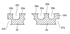
- FIG. 11 is a cross-sectional view showing more detailed shapes of the lead frame 20 and the lead frame 22 formed by etching.
- the gaps 25, 25 b, 25 c of the lead frames 20, 22 formed by etching are so-called barrels that once spread from the top surface to the bottom surface in the longitudinal section (cross section in FIG. 11 and zx) and then narrow toward the bottom surface. It has a mold shape. For this reason, the adhesiveness of the resin of the resin part 10 and the lead frames 20 and 22 can be improved.
- Etching is performed so as to penetrate through the lead frame 22 (cutout of the outer shape of the lead frame. For example, between the lead frame 20 and the lead frame 22 in FIG. 11) Processing may be performed (that is, formation of the convex portions 20a, 20b, 20c, 22a, and 22b).
- Processing may be performed (that is, formation of the convex portions 20a, 20b, 20c, 22a, and 22b).
- two barrel shapes are aligned vertically (z-axis direction) as shown between the lead frame 20 and the lead frame 22 in FIG.
- a shape may be formed to improve the adhesion to the resin.
- etching method dry etching and wet etching can be used.
- etchant an appropriate one corresponding to the material of the lead frames 20 and 22 may be selected. Etching conditions vary depending on the type of metal used, but when copper is used for the lead frame, for example, as an etchant, persulfate or hydrogen peroxide and inorganic acid, iron chloride or copper chloride and inorganic acid, ammonia copper complex salt It is suitable to use a general copper soft etching solution made of an ammonium salt or the like.
- the lead frames 20 and 22 obtained in the above-described S1 step are placed in the mold, and the resin 30 is poured into the package 30 by the transfer molding method.
- a separable mold composed of an upper mold and a lower mold is preferably used for improving workability.
- the upper surface of each of the convex portions 20a, 20b, and 22a is brought into contact with the portion of the mold that forms the concave portion 12 of the resin portion 10, so that the bottom surface 14 and the upper surfaces of the convex portions 20a, 20b, and 22a are flush with each other.
- the upper surfaces of the convex portions 20a, 20b, and 22a can be exposed from the resin portion.
- burrs generated in the package 30, such as resin that covers the upper surfaces of the protrusions 20a, 20b, 22a, blasting, electrolytic solution method (alkali, etc.), or combinations thereof, etc. To remove.
- the lead frame 20 and / or the lead frame 22 are plated as necessary, for example, to improve reflectivity.
- the plating process is a preferable process in order to project the protrusions 20 a, 20 b, and 22 b from the surface of the resin part 10 on the bottom surface 14 of the recess 12.
- the resin molding is performed in step S2
- the upper surface of the convex portions 20a, 20b, and 22b and the bottom surface 14 of the resin portion 10 are made flush with each other, and then the main plating process is performed.
- the convex portions 20 a, 20 b, and 22 b can be protruded from the surface of the resin portion 10 at the bottom surface 14.
- electrolytic plating or electroless plating can be used as the plating method.
- electrolytic plating By forming by electrolytic plating, a metal layer can be selectively formed only on the convex portions 20a, 20b, and 22a exposed from the resin portion 10.
- the light emitting element 50 is mounted on the upper surface of the convex portion 20a. It is preferable to perform eutectic bonding using an Au—Sn alloy. Alternatively, the light emitting element 50 may be fixed using a resin paste, a silicon paste, or a silver paste. After fixing the light emitting element 50, the light emitting element 50, the lead frame 20, and the lead frame 22 are electrically connected by wire bonding using the wires 40 and 42.
- the lead frame 20 and / or the lead frame 22 is plated and then resin molding is performed. Therefore, the upper surfaces of the plated protrusions 20a, 20b, and 22a It can be easily flush with the bottom surface 14.
- the reflectance is improved by applying to the lead frame 20 and / or the lead frame 22, and the top surface and the bottom surface 14 of the convex portions 20a, 20b, and 22a are in the same plane as in the embodiment shown in FIG.
- the light emitting device 100 can be easily obtained.
- the light emitting devices 100A and 100B can be manufactured by the same method. More specifically, regarding the light emitting device 100A, the number of lead frames and the number of light emitting elements increases, and in addition to the light emitting element 50 in S5: light emitting element mounting step, a Zener diode 55 or the like is added as necessary. It can be manufactured by mounting the element. On the other hand, the light emitting device 100B does not shape the concave portion in the resin portion 10B in the resin molding process, and seals with the sealing material instead of inserting the sealing material into the concave portion in the sealing step performed as necessary. It can be manufactured by forming the stop member 18.
Landscapes
- Engineering & Computer Science (AREA)
- General Engineering & Computer Science (AREA)
- Led Device Packages (AREA)
Abstract
パッケージの発光素子が配置された素子載置面の反射率を向上させることにより高い電力効率を有すると共に、発光素子の発熱を容易に放熱できる発光装置を提供する。 樹脂部と、該樹脂部の内部に配置された1つ以上のリードフレームとを含むパッケージと、該リードフレームの少なくとも1つと電気的に接続された発光素子と、 を含む発光装置であって、前記リードフレームの少なくとも1つは、上面に少なくとも1つの凸部を有し、該少なくとも1つの凸部は、その側面が前記樹脂部により囲まれ、且つ、その上面である凸部上面が前記樹脂部より露出し、前記発光素子が該凸部上面に載置され、該凸部上面の面積の少なくとも半分が前記発光素子により覆われていることを特徴とする発光装置である。
Description
本発明は、照明器具、ディスプレイ、携帯電話および携帯端末のバックライト、動画照明補助光源を含む各種の光源に用いられる発光装置に関する。
発光ダイオード(LED)およびレーザーダイオード(LD)等の発光素子を用いる発光装置は、小型で高い発光効率を有し、また鮮明な光を発光することが可能である。さらに、初期駆動特性に優れ、振動およびオン・オフの繰り返しに対して優れた耐久性を示す。このため発光素子を有する発光装置は各種の光源として用いられている。
このような発光装置では、発光素子から発せられた光を効率よく目的とする方向に反射させる必要がある。このため、多くの発光装置では、例えば特許文献1(同文献の図1および図2参照)に示されるように、側面が樹脂等から形成され、底面は樹脂とともに金属より成るリードフレームが配置された凹部(キャビティー)をパッケージ等に設け、凹部内においてリードフレーム上に発光素子を配置した構成が用いられる。
このような構成を用いることで、発光素子から直接凹部の上部に到達した光に加えて、発光素子から出て凹部の側面または底面で反射された光も発光装置の外部に発光させることが可能となり、電力効率(発光効率)を高めることができる。
このような構成を用いることで、発光素子から直接凹部の上部に到達した光に加えて、発光素子から出て凹部の側面または底面で反射された光も発光装置の外部に発光させることが可能となり、電力効率(発光効率)を高めることができる。
また、凹部底面での金属フレームの露出をより少なくした構成として、特許文献2(例えば同文献の図3参照)には、一様な厚みを有するリードフレームを屈曲させてリードフレームの上面に突出部(曲げ出し部)を設けて、この突出部の上に発光素子を載置するとともに、リードフレームの上面のうち、突出部以外は樹脂で被覆して凹部の底部から露出させない発光装置が開示されている。
しかし、リードフレームは発光素子が発する熱を吸収し、発光装置外に放熱するヒートシンクとしての機能を有する。このため、発光素子の直下部だけにリードフレームを配置すると、リードフレームの体積が少ないため、発光素子の発熱を充分に吸収することができなくなる。このため、より大きなリードフレームを用いることから、より広いリードフレームの表面、とりわけ発光素子が載置されていない部分が凹部(キャビティー)の底面において露出することになる。
樹脂はその種類、色等を適正に選択することで例えば80%以上のように容易に高い反射率を得ることができる。これに対して、リードフレームは例えば鉄合金、リン青銅を含む銅合金、ニッケル合金等の金属から成り、これらの金属は樹脂に比べると反射率が低いという問題がある。
従って、従来の発光装置では、パッケージに設けた凹部の底面の面積の一定割合以上を光の反射率が大きいリードフレームが占めることから、よりいっそうの電力効率の向上が困難であるという問題があった。
また、リードフレームの反射率を向上させる方法として、反射率の高い銀をめっき等によりリードフレームに被覆する方法が知られている。しかし、銀は時間の経過と共に大気または樹脂中でも腐食し、表面が変色して反射率が低下してしまうため、銀めっきによる被覆は恒久的な対策とはならない場合が多い。
一方、特許文献2に記載の発光装置では、上述のようにリードフレームの上面のうち、突起部以外が樹脂に覆われているため、高い反射率を得ることはできる。しかし、突起部等を、リードフレーム材料を屈曲させて形成することから、リードフレームの成形精度が低く、容易には所望の特性が得られない場合がある、および製品歩留まりが低い場合が多いという問題があった。
さらに、厚さが一様のリードフレーム用材料を屈曲させて所望の形状のリードフレームを得るため、リードフレームの厚さが限定され、例えば発光素子の直下からパッケージの樹脂部を貫通し発光装置の裏面にリードフレームを露出させることができず発光素子の発熱を充分に放熱できない場合があるという問題もあった、
さらに、厚さが一様のリードフレーム用材料を屈曲させて所望の形状のリードフレームを得るため、リードフレームの厚さが限定され、例えば発光素子の直下からパッケージの樹脂部を貫通し発光装置の裏面にリードフレームを露出させることができず発光素子の発熱を充分に放熱できない場合があるという問題もあった、
そこで本発明は、発光素子が配置されるパッケージの凹部の底面等、パッケージの発光素子が配置された素子載置面の反射率を向上させることにより高い電力効率を有すると共に、発光素子の発熱を容易に放熱できる発光装置を提供することを目的とする。
本発明の態様1は、樹脂部と、該樹脂部の内部に配置された1つ以上のリードフレームとを含むパッケージと、該リードフレームの少なくとも1つと電気的に接続された発光素子と、を含む発光装置であって、前記リードフレームの少なくとも1つは、上面に少なくとも1つの凸部を有し、該少なくとも1つの凸部は、その側面が前記樹脂部により囲まれ、且つ、その上面である凸部上面が前記樹脂部より露出し、前記発光素子が該凸部上面に載置され、該凸部上面の面積の少なくとも半分が前記発光素子により覆われていることを特徴とする発光装置である。
本願発明の態様1に係る発光装置では、詳細は後述するが、上面に少なくとも1つの凸部を有しているリードフレームを少なくとも1つ含む。この少なくとも1つの凸部が樹脂部より露出しており、この露出した凸部の上に、必要に応じて接着作用を有する共晶合金またはペーストを介して、発光素子が載置されている。そして、凸部上面の面積の少なくとも半分が発光素子により覆われている。
このように、凸部上面の面積の少なくとも半分が発光素子により覆われていることで、反射率の低いリードフレームの露出を低減でき、高い反射率を得ることができる。
一方、発光素子の発熱により生じた熱は、発光素子直下の凸部を通じて、リードフレーム全体に広がることが可能であり、よって容易にリードフレームにより吸収され、その後発光装置の外に放熱される。
一方、発光素子の発熱により生じた熱は、発光素子直下の凸部を通じて、リードフレーム全体に広がることが可能であり、よって容易にリードフレームにより吸収され、その後発光装置の外に放熱される。
本発明の態様2は、記発光素子の底面の面積が、凸部上面の面積に対して50%~150%であることを特徴とする態様1に記載の発光装置である。
本発明の態様3は、前記発光素子の底面の縦の長さおよび横の長さが、それぞれ、凸部上面の縦の長さおよび横の長さに対してプラスマイナス0.1mmの範囲内であることを特徴とする態様1~4のいずれかに記載の発光装置である。
本発明の態様4は、凸部上面の形状が、角が丸められた形状であることを特徴とする態様1または2に記載の発光装置である。
本発明の態様5は、前記凸部上面の面積が前記発光素子の底面の面積よりも小さく、前記素子載置面において、前記発光素子が前記凸部上面の外側まで載置されることを特徴とする態様1~4のいずれかに記載の発光装置である。
本発明の態様6は、前記凸部上面の面積が、前記発光素子の底面の面積と同じであることを特徴とする態様1~4のいずれかに記載の発光装置である。
本発明の態様7は、前記素子載置面において、前記凸部上面が、前記樹脂部の表面から突出していることを特徴とする態様1~6のいずれかに記載の発光装置である。
本発明の態様8は、前記リードフレームの下面において、前記発光素子が載置された前記凸部の直下部分が、前記樹脂部から露出していることを特徴とする態様1~7のいずれかに記載の発光装置である。
本発明の態様9は、前記樹脂部が凹部を有し、前記素子載置面が該凹部の底面であることを特徴とする態様1~8のいずれか1項に記載の発光装置である。
本発明の態様10は、前記リードフレームが、前記凸部を少なくとも2つ有し、該少なくとも2つの凸部の間に、前記樹脂部の樹脂が充填されていることを特徴とする態様1~9のいずれか1項に記載の発光装置である。
本発明の態様11は、樹脂部と、該樹脂部の内部に配置された1つ以上のリードフレームとを含むパッケージと、該リードフレームの少なくとも1つと電気的に接続され、前記パッケージの素子載置面に配置された発光素子と、を含む発光装置であって、前記リードフレームの少なくとも1つは、上面に少なくとも2つの凸部を有し、該少なくとも2つの凸部の間に、前記素子載置面を形成する樹脂を含み、前記凸部の少なくとも1つが前記素子載置面において前記樹脂部より露出した凸部上面を有し、該凸部上面に前記発光素子が載置されていることを特徴とする発光装置である。
本願発明の態様11に係る発光装置では、詳細は後述するが、上面に少なくとも2つの凸部を有しているリードフレームを少なくとも1つ含む。そして、この2つの凸部の間の隙間にパッケージの素子載置面(例えばパッケージの凹部)の一部を形成する樹脂が存在する(入り込んでいる)。また、この凸部の少なくとも1つが発光素子を載置する素子載置面において、樹脂部より露出しており、この露出した凸部の上に、必要に応じて接着作用を有する共晶合金またはペーストを介して、発光素子が載置されている。従って、この樹脂部の1つの面は、発光素子からの光を反射する反射面として機能する。
このように、2つの凸部の間の隙間に樹脂が入り込むことで、発光素子が配置されている素子載置面において、反射率の低いリードフレームの露出を低減でき、高い反射率を得ることができる。
一方、2つの凸部は樹脂部内で繋がっていることから、発光素子の発熱により生じた熱は、発光素子直下の凸部を通じて、もう一方の凸部を含むリードフレーム全体に広がることが可能であり、よって容易にリードフレームにより吸収され、その後発光装置の外に放熱される。
一方、2つの凸部は樹脂部内で繋がっていることから、発光素子の発熱により生じた熱は、発光素子直下の凸部を通じて、もう一方の凸部を含むリードフレーム全体に広がることが可能であり、よって容易にリードフレームにより吸収され、その後発光装置の外に放熱される。
本発明の態様12は、前記樹脂部が凹部を有し、前記素子載置面が該凹部の底面であり、前記凹部の側面と該凹部の底面との接続部分が前記少なくとも2つの凸部の間の上部に位置することを特徴とする態様11に記載の発光装置である。
本発明の態様13は、前記リードフレームの少なくとも1つが、前記素子載置面において前記樹脂部より露出した凸部上面を有する凸部を少なくとも2つ有し、該凸部のうち一方に前記発光素子が載置されており、他方に前記発光素子と電気的に接続されたワイヤが接続されていることを特徴とする態様11または12に記載の発光装置である。
本願発明に係る発光装置は、光発光素子が配置されるパッケージの素子載置面において、リードフレームの露出を容易に抑えて反射率を向上させることが可能であり、これにより高い電力効率を得ることができる。さらに、発光素子の発熱を容易に放熱することが可能である。
以下、図面に基づいて本発明の実施形態を詳細に説明する。なお、以下の説明では、必要に応じて特定の方向や位置を示す用語(例えば、「上」、「下」、「右」、「左」及びそれらの用語を含む別の用語)を用いるが、それらの用語の使用は図面を参照した発明の理解を容易にするためであって、それらの用語の意味によって本発明の技術的範囲が制限されるものではない。また、複数の図面に表れる同一符号の部分は同一の部分又は部材を示す。
図1は本願発明に係る発光装置100の平面図であり、図2は図1のII-II断面を示す断面図である。また、図3は、理解を容易にするために、図1に示す発光装置100のうち発光素子50とワイヤ40、42の記載を省略した平面図であり、すなわち発光装置100のパッケージ30の平面図を示す。図4は図3のIV-IV断面を示す断面図であり、図5は図3のV-V断面を示す断面図である。
パッケージ30は、上面に凹部(キャビティー)12を有する樹脂部(パッケージ本体)10と、樹脂部10の内部でかつ少なくとも一部が凹部12の下(直下)に位置する少なくとも1つのリードフレームとを有している。図1および図3に示す実施形態では、リードフレーム20、22の2つのリードフレームを有している。発光装置100は、更に凹部12の内部でリードフレーム20の上に配置されている発光素子50を含む。発光素子50は、必要に応じてワイヤ等を用いて、少なくとも1つのリードフレームと電気的に接続されており、図1および図3に示す実施形態では、ワイヤ40によりリードフレーム20と接続され、ワイヤ42によりリードフレーム22と接続されている。
凹部12は、好ましくは、図示するように詳細を後述する封止材が充填されている。
このような構成および効果を有する発光装置の100について以下に詳述する。
凹部12は、好ましくは、図示するように詳細を後述する封止材が充填されている。
このような構成および効果を有する発光装置の100について以下に詳述する。
(1)発光装置
・リードフレーム20
樹脂部10の内部に配置されているリードフレーム20の上面は、少なくとも1つ(例えば、詳細を後述する凸部20a)、好ましくは少なくとも2つの凸部を含む。図1~図5に示す実施形態では3つの凸部(例えばz方向の厚さが増加している部分)20a、20b、20cを有している。凸部20aと凸部20bは、樹脂部10の凹部12の底面14の下に位置している。すなわち、発光装置100では、凸部の少なくとも1つは樹脂部10の凹部12の底面14の下(直下)に位置している。そして、凸部20aの上面(「頂面」ともいう)は、樹脂部10の樹脂に覆われておらず、すなわち凹部12の底面14において、樹脂部10より露出している。
好ましくは、図示するように凸部20bの上面(頂面)も素子載置面において樹脂部10底面14より露出している。
なお、底面14とは、樹脂部の10を構成する樹脂より成る部分に加えて、樹脂部10(樹脂10を構成する樹脂)から露出した凸部の上面(図3および図4の実施形態では、リードフレーム20の凸部20aの上面と凸部20bの上面に加えて、詳細を後述するリードフレーム22の凸部22aの上面)を含む。
また、底面14は、発光素子50を配置する素子載置面に相当する。
・リードフレーム20
樹脂部10の内部に配置されているリードフレーム20の上面は、少なくとも1つ(例えば、詳細を後述する凸部20a)、好ましくは少なくとも2つの凸部を含む。図1~図5に示す実施形態では3つの凸部(例えばz方向の厚さが増加している部分)20a、20b、20cを有している。凸部20aと凸部20bは、樹脂部10の凹部12の底面14の下に位置している。すなわち、発光装置100では、凸部の少なくとも1つは樹脂部10の凹部12の底面14の下(直下)に位置している。そして、凸部20aの上面(「頂面」ともいう)は、樹脂部10の樹脂に覆われておらず、すなわち凹部12の底面14において、樹脂部10より露出している。
好ましくは、図示するように凸部20bの上面(頂面)も素子載置面において樹脂部10底面14より露出している。
なお、底面14とは、樹脂部の10を構成する樹脂より成る部分に加えて、樹脂部10(樹脂10を構成する樹脂)から露出した凸部の上面(図3および図4の実施形態では、リードフレーム20の凸部20aの上面と凸部20bの上面に加えて、詳細を後述するリードフレーム22の凸部22aの上面)を含む。
また、底面14は、発光素子50を配置する素子載置面に相当する。
樹脂部10の底面14より露出している凸部20aの上面には、発光素子50が載置されている(すなわち、凸部20aの上面は、発光素子実装パターンとして機能する)。
発光素子50は、Au-Sn合金等を用いた共晶接合またはシリコンペースト、銀ペーストもしくは樹脂ペーストのようなペーストを用いて固定してよい。
発光素子50は、Au-Sn合金等を用いた共晶接合またはシリコンペースト、銀ペーストもしくは樹脂ペーストのようなペーストを用いて固定してよい。
凸部20a、20b、20cは、好ましくは、高さ(図1、2のz方向)が、リードフレーム20の厚みの略半分もしくはそれよりも小さい。具体的には、底面14までの高さ(フレーム20の凸部が部分の上面から凸部の上面まで高さ)が、0.2mm以下、さらには0.01mm~0.1mmであることが好ましい。上面の縦(図1、2のx方向)および横(図1、2のy方向)は、該上面に載置される発光素子50やワイヤ40等の接着に十分な面積となるように設定することが好ましい。発光素子50を載置する場合には、発光素子50の底面の面積が、凸部20aの上面の面積に対して50%~150%であることが好ましい。これによって、良好な放熱性と良好な発光素子実装性とを両立させることができる。ワイヤ40が接合される凸部20bの面積は、発光素子50が載置される凸部20aの面積と略同一か、それよりも小さくよい。
また、凸部20a、20b、20cは、それぞれ最も近接する凸部(同じリードフレームの凸部)間の距離を、加工方法によるが、例えばエッチングを用いる場合であれば、0.1mm程度まで小さくすることができる。好ましくは0.1mm以上とする。
また、凸部20a、20b、20cは、それぞれ最も近接する凸部(同じリードフレームの凸部)間の距離を、加工方法によるが、例えばエッチングを用いる場合であれば、0.1mm程度まで小さくすることができる。好ましくは0.1mm以上とする。
発光素子50は、リードフレーム20と電気的に接続されてよい。好ましい接続形態の1つは、図示するように、凸部20bの上面と発光素子50とをワイヤで接続することである(すなわち、凸部20bの上面は、ワイヤパターンとして機能する)。
なお発光素子50はリードフレーム20と電気的に接続されなくてもよい。例えば、リードフレーム20が凸部を1つしか有せず(例えば、凸部20a)、この唯一の凸部の上面に、発光素子50が載置されている場合には、発光素子50はリードフレーム20と電気的に接続されなくてもよい。
なお発光素子50はリードフレーム20と電気的に接続されなくてもよい。例えば、リードフレーム20が凸部を1つしか有せず(例えば、凸部20a)、この唯一の凸部の上面に、発光素子50が載置されている場合には、発光素子50はリードフレーム20と電気的に接続されなくてもよい。
リードフレーム20の凸部20aと凸部20bとの間の隙間(凹部)25aは、樹脂部10の樹脂で満たされており、隙間25aに存在する樹脂は、隙間25aの上端で樹脂部10の凹部12の底面14の一部を形成している。
好ましくは、図示するように、凸部20bと凸部20cとの間の隙間25bも、樹脂部10の樹脂で満たされており、この隙間25bに存在する樹脂も隙間25bの上端で樹脂部10の凹部12の底面14の一部を形成している。
このように、前記リードフレーム20は、上面に少なくとも2つの凸部を有する場合、該少なくとも2つの凸部の間に形成された隙間に樹脂部10の底面14を形成する樹脂が存在している。さらに、リードフレーム20の上面の凸部の少なくとも1つ(凸部20a)が底面14において、樹脂部10より露出し、この露出した凸部20aの上面に発光素子50が載置されている。
以上述べたように、リードフレーム20の隙間25aおよび隙間25bに樹脂が充填され、この樹脂が凹部12の底面14を形成していることから、凹部の底面14において、反射率が低い金属フレーム20の露出を低減し、反射率が高い樹脂の割合を増やすことができる。このことは、発光素子から凹部12の底面14に到達した光がより多く反射され、この結果、より多くの光が発光装置100から外部に出ていくことを意味する。すなわち発光装置100は、より高い発光効率を有することになる。
また、通電することにより、発光素子50を発光させた際に生ずる発熱は、凸部20aの上面を介してリードフレーム20内を伝導する。リードフレーム20は、発光素子50の直下だけでなく、図2の横方向(図のx方向)に広がって配置され、充分な体積を有することから、発光素子50が発する熱を充分に吸収し、発光装置100の外部に放熱することが可能である。特に、発光素子50の直下においてリードフレーム20の底面(下面)が樹脂部10から露出していることで、さらに効率的に放熱できる。図2に示すように、発光素子50が載置された凸部20aは、発光素子50の載置面と対向する面(裏面)が、樹脂部10から露出されていること(すなわち、リードフレーム20の下面において、凸部20aの直下部分が樹脂部10から露出していること)が好ましい。
図2および図4に示すように、パッケージ30の側面および/または底面において、樹脂部10よりリードフレーム20を露出させることが好ましい。これにより発光素子50からの発熱をより効率的に発光装置の外に放熱できるからである。この好ましい実施形態の詳細は後述する。
図2および図4に示すように、パッケージ30の側面および/または底面において、樹脂部10よりリードフレーム20を露出させることが好ましい。これにより発光素子50からの発熱をより効率的に発光装置の外に放熱できるからである。この好ましい実施形態の詳細は後述する。
また、隙間25aおよび隙間25bに樹脂が入り込み、これら入り込んだ樹脂は凸部20a、20b、20cの側面と接着(結合)し、更には隙間25a、25bの底面(隙間25a、25bにおけるリードフレームの上面)とも接着していることから、樹脂部10の樹脂とリードフレーム22とが接着している面積を増加できる。これにより、樹脂部10とリードフレーム20とが剥離するリスクを低減することができる。
・リードフレーム22
発光装置100は、図示するようにリードフレーム(第2のリードフレーム)22を有してよい。リードフレーム22もリードフレーム(第1のリードフレーム)20と同様に、樹脂部10内に配置され、少なくとも一部が底面14の下に位置している。リードフレーム22は上面に2つの凸部22a、22bを有しており、凸部22aは、凹部12の底面14の下に位置している。そして、凸部22aの上面(「頂面」ともいう)は、樹脂部10の樹脂に覆われておらず、底面14において樹脂部10より露出している。
発光装置100は、図示するようにリードフレーム(第2のリードフレーム)22を有してよい。リードフレーム22もリードフレーム(第1のリードフレーム)20と同様に、樹脂部10内に配置され、少なくとも一部が底面14の下に位置している。リードフレーム22は上面に2つの凸部22a、22bを有しており、凸部22aは、凹部12の底面14の下に位置している。そして、凸部22aの上面(「頂面」ともいう)は、樹脂部10の樹脂に覆われておらず、底面14において樹脂部10より露出している。
凸部22a、22bは、好ましくは、高さが(図1、2のz方向)がリードフレーム22の厚みの略半分もしくはそれよりも小さい。具体的には、底面14までの高さが、0.2mm以下、さらには0.01mm~0.1mmであることが好ましい。上面の縦(図1、2のx方向)および横(図1、2のy方向)は、ワイヤ42等の接着に十分な面積となるように設定することが好ましい。ワイヤ42が接合される凸部22aの面積は、発光素子50が載置される凸部20aの面積と略同一か、それよりも小さくすることが好ましい。また、凸部22a、22bは、それぞれ最も近接する凸部(同じリードフレームの凸部)間の距離を、加工方法によるが、例えばエッチングを用いる場合であれば、0.1mm程度まで小さくすることができる。好ましくは0.1mm以上とする。
発光素子50は、凸部22aの上面とワイヤ42を介して電気的に接続されている(すなわち、凸部22aの上面は、ワイヤパターンとして機能する)。
リードフレーム22の凸部22aと凸部22bとの間の隙間(凹部)25cは、樹脂部10の樹脂で満たされており、この隙間25cを満たす樹脂は、隙間25cの上端で樹脂部10の凹部12の底面14の一部を形成している。
このように、隙間25cに樹脂が充填され、この樹脂が凹部12の底面14の一部を形成していることから、凹部12の底面14において反射率が低い金属フレーム22の露出を低減し、反射率が高い樹脂の割合を増やすことができる。このことは、発光素子50から凹部12の底面14に到達した光がより多く反射され、この結果、より多くの光が発光装置100から外部に出ていくことを意味する。すなわち発光装置100は、2つのリードフレーム20、22を含んでいるにもかかわらず、高い電力効率を得ることができる。
また、隙間25cに樹脂が入り込み、この樹脂は凸部22a、22bの側面と接着(結合)し、更には隙間25cの底面(隙間25cにおけるリードフレーム22の上面)とも接着することから、樹脂部10の樹脂とリードフレーム22とが接着している面積を増加できる。これにより、樹脂部10とリードフレーム22とが剥離するリスクを低減することができる。
より好ましくは、図2および図4に示すように、隙間25cは、樹脂部10の凹部12の底面14と凹部12の側面16との接続部分(底面14と側面16が交わる部分)の下(直下)に位置する。すなわち、凹部12の側面16と凹部12の底面14との接続部分が凸部22aと凸部22bの間の上部(凸部22aと凸部22bの間の隙間25cの上部)に位置する。
応力が集中し、剥離の起点となりやすい、底面14と側面16との接続部分に、リードフレーム22が存在しない状態を確実に実現できることから、樹脂部10とリードフレーム22との剥離をより確実に防止できる。
応力が集中し、剥離の起点となりやすい、底面14と側面16との接続部分に、リードフレーム22が存在しない状態を確実に実現できることから、樹脂部10とリードフレーム22との剥離をより確実に防止できる。
リードフレーム20についても同様の構成を有することが、より好ましい。すなわち、図2および図3に示すように、より好ましくは、隙間25bは、樹脂部10の凹部12の底面14と凹部12の側面16との接続部分(底面14と側面16が交わる部分)の下(直下)に位置する。
これによりリードフレーム20についても同様の効果を得ることができる。
これによりリードフレーム20についても同様の効果を得ることができる。
図6は、発光装置100の底面と側面の示す斜視図である。
リードフレーム20は、好ましくは、図2、図4および図5に示すように、その側面(図2および図4では右側の側面)および/または底面(図2および図4では下面、図5では上面として示されている)が樹脂部10から露出している。これにより、発光素子50の発熱をより容易に発光装置100の外部に放熱できる。
この場合、リードフレームの底面において、例えば図2およぶ図4に示すように、発光素子50が載置されている凸部20aの直下部分が、樹脂部10より露出していることがより好ましい。
さらに、このようにリードフレーム20の表面の一部が外部に露出することで、リードフレーム20と、例えば発光装置100を実装する実装基板の電極等の電気接点とを容易に電気的に接続できる。
リードフレーム20は、好ましくは、図2、図4および図5に示すように、その側面(図2および図4では右側の側面)および/または底面(図2および図4では下面、図5では上面として示されている)が樹脂部10から露出している。これにより、発光素子50の発熱をより容易に発光装置100の外部に放熱できる。
この場合、リードフレームの底面において、例えば図2およぶ図4に示すように、発光素子50が載置されている凸部20aの直下部分が、樹脂部10より露出していることがより好ましい。
さらに、このようにリードフレーム20の表面の一部が外部に露出することで、リードフレーム20と、例えば発光装置100を実装する実装基板の電極等の電気接点とを容易に電気的に接続できる。
同様に、リードフレーム22は、好ましくは図2、図4および図5に示すように、その側面(図2および図4では左側の側面)および/または底面(図2および図4では下面、図5では上面として示されている)が樹脂部10から露出している。このようにリードフレーム22の表面の一部が外部に露出することで、リードフレーム22と、例えば発光装置100を実装する実装基板の電極等の電気接点とを容易に電気的に接続できる。
図2、図4および図5に示す実施形態に係る発光装置100において、例えば、実装基板に配置された電極上に、ハンダ等を用いてリードフレーム20、22のそれぞれの底面を固定することで、リードフレーム20およびリードフレーム22をそれぞれ、外部電極と電気的に接続することができる。
この場合、好ましくは、リードフレーム20は、露出した底面および側面に切り欠き(窪み)27aを有する。同様に、好ましくは、リードフレーム22は、露出した底面および側面に切り欠き27bを有する。
リードフレーム20およびリードフレーム22の底面を、ハンダを用いて実装基板の電極に固定する際に、切り欠き27aおよび切り欠き27bの内部にハンダが入り込む。これにより、より安定して、リードフレーム20およびリードフレーム22をそれぞれ、電極に固定でき、この結果、リードフレーム20およびリードフレーム22をそれぞれ、より安定して電気的に接続できる。
リードフレーム20およびリードフレーム22の底面を、ハンダを用いて実装基板の電極に固定する際に、切り欠き27aおよび切り欠き27bの内部にハンダが入り込む。これにより、より安定して、リードフレーム20およびリードフレーム22をそれぞれ、電極に固定でき、この結果、リードフレーム20およびリードフレーム22をそれぞれ、より安定して電気的に接続できる。
・樹脂部の凹部の底面とリードフレームの凸部上面との位置関係
次に、凹部10の底面14と凸部20aの上面の位置関係について詳細を説明する。
底面14の好ましい実施形態の1つでは、図2および図4に示すように、底面14は平面となっている。すなわち、リードフレーム20の凸部20a、20bのぞれぞれの上面と、リードフレーム22の凸部22aの上面と、底面14のそれ以外の部分(すなわち樹脂より成る部分)とが、同一平面内に存在する(面一になっている)状態である。このような状態は、金型内にリードフレーム20および22を配置して、トランスファーモールド法により、樹脂を流し込んでパッケージ30を形成する際に、凹部12形成する金型の部分に部20a、20b、22aのそれぞれの上面を接触させることで容易に形成することができる。
次に、凹部10の底面14と凸部20aの上面の位置関係について詳細を説明する。
底面14の好ましい実施形態の1つでは、図2および図4に示すように、底面14は平面となっている。すなわち、リードフレーム20の凸部20a、20bのぞれぞれの上面と、リードフレーム22の凸部22aの上面と、底面14のそれ以外の部分(すなわち樹脂より成る部分)とが、同一平面内に存在する(面一になっている)状態である。このような状態は、金型内にリードフレーム20および22を配置して、トランスファーモールド法により、樹脂を流し込んでパッケージ30を形成する際に、凹部12形成する金型の部分に部20a、20b、22aのそれぞれの上面を接触させることで容易に形成することができる。
このように金型と凸部の上面が接した状態で樹脂を流し込むため、凸部20a、20b、22aの上面が樹脂で覆われることなく、あるいはたとえ樹脂に覆われても樹脂が極めて薄いため、バリ取りで簡便に除去できるため、極めて容易に凸部20a、20b、22aの上面を露出させることができるという利点がある。
このような形態を有する底面14においては、凸部20aの上面に載置される発光素子50の大きさ、より詳細には凸部20aの上面に載置される部分である、発光素子50の底面の大きさは、縦(図1および図2のx方向)および横(同y方向)とも、それぞれ、凸部20aの上面の縦および横に対してプラスマイナス0.1mmの範囲内であることが好ましい。この範囲内であれば、凸部20aの上面のうち、発光素子50により覆われておらず、従って、反射率が低い部分(銀めっきが腐食により変色した場合も含む)が少なく、底面14がより高い反射率を維持できるからである。さらに、発光素子50の底面の大きさがこの範囲にあれば、所謂セルフアライメント効果を得ることができる。すなわち、発光素子50の底面と、凸部20aの上面の外形が概ね同じ(形状が対応している)であることから、例えば共晶接合法等に発光素子50を凸部20aの上面に固定しようとすると、接合時に発光素子50の底面が、自動的に凸部20aの上面の中央に位置するように移動することから、極めて高い実装精度で発光素子50を実装できる。凸部20aの上面の形状は、発光素子50の平面視形状と対応した形状であることが好ましい。例えば、発光素子50の平面視形状が略正方形であれば、凸部20aの上面の形状も略正方形とする。凸部20aの上面の形状は、図3に示すように、角が丸められた形状(すなわち、多角形であって、その角の一部または全部(少なくとも一部)が丸められている形状)であってもよい。このような形状とすることで、発光素子50を接着する接着材料との濡れ性を向上することができる。特に共晶接合等、金属を含む接着材料によって発光素子50を接着する場合に好ましい。
このような、発光素子の底面の大きさと凸部20の上面の大きさとの好ましい関係は、縦横の長さに代えて、面積で規定することも可能である。具体的には、発光素子50の底面の面積は、凸部20の上面の面積に対して50%~150%の範囲が好ましい。この面積範囲が好ましい理由は、上述の縦横の大きさ範囲と同じである。
すなわち、凸部20の上面の面積の少なくとも半分(50%以上)が、発光素子50(発光素子50の底面)により覆われている。これにより、凸部20aの上面のうち、発光素子50により覆われておらず、従って、反射率が低い部分(銀めっきが腐食により変色した場合も含む)が少なくなり、底面14がより高い反射率を維持できる。
すなわち、凸部20の上面の面積の少なくとも半分(50%以上)が、発光素子50(発光素子50の底面)により覆われている。これにより、凸部20aの上面のうち、発光素子50により覆われておらず、従って、反射率が低い部分(銀めっきが腐食により変色した場合も含む)が少なくなり、底面14がより高い反射率を維持できる。
・樹脂部の凹部の底面とリードフレームの凸部上面との位置関係の別の実施形態
図7は、樹脂部10の凹部12の底面14と凸部上面との位置関係の別の実施形態を示す断面図である。図7に示す実施形態では、リードフレーム20の凸部20aは底面14において、樹脂部10の表面(底面14のうち、凸部20aの上面、凸部20bの上面および凸部22aの上面以外の部分)から突出している。この場合、好ましくは、図7に示すように、リードフレーム20の凸部20bおよびリードフレーム22の凸部22aも同様に突出している。
このようなリードフレームの凸部の突出は、例えば、リードフレーム20とリードフレーム22とを金型に配置し、トランスファーモールド法により、樹脂を流し込んでパッケージ30を形成する際に、金型形状を調整して、樹脂部10の底面14と成る面を凸部20a、20b、22aそれぞれの上面よりよりも低くなるようすることで得ることができる。
図7は、樹脂部10の凹部12の底面14と凸部上面との位置関係の別の実施形態を示す断面図である。図7に示す実施形態では、リードフレーム20の凸部20aは底面14において、樹脂部10の表面(底面14のうち、凸部20aの上面、凸部20bの上面および凸部22aの上面以外の部分)から突出している。この場合、好ましくは、図7に示すように、リードフレーム20の凸部20bおよびリードフレーム22の凸部22aも同様に突出している。
このようなリードフレームの凸部の突出は、例えば、リードフレーム20とリードフレーム22とを金型に配置し、トランスファーモールド法により、樹脂を流し込んでパッケージ30を形成する際に、金型形状を調整して、樹脂部10の底面14と成る面を凸部20a、20b、22aそれぞれの上面よりよりも低くなるようすることで得ることができる。
しかし、好ましくは、上述したように、リードフレーム20の凸部20a、20bのぞれぞれの上面と、リードフレーム22の凸部22aの上面と、底面14のそれ以外の部分(すなわち樹脂より成る部分)とが、同一平面内に存在する(面一になっている)状態にした後、凸部20a、20b、22aのそれぞれの上面がそれぞれめっき層(金属層)21a、21b、21cを有するように、めっき処理行うことで、より容易に凸部の上面を底面14において、樹脂部10の表面から突出させることができる。
めっき層21a、21b、21cは、例えば、銀、金、ニッケル、パラジウム、銅、錫等より選択される金属めっきまたはこれらを組み合わせた合金めっきより成る。好ましくは、反射率の高い銀や、ワイヤと良好な密着性を有する金を選択する。めっき層21a、21b、21cは、樹脂部10を形成後、電解めっきにより形成することで、凸部20a、20b、22aのみに選択的に形成することができる。また、めっき層21a、21b、21cは、全て同一の材料とすることで、同一の工程で形成できる。
このようにリードフレームの凸部上面を底面14において、樹脂部10の表面から突出させることにより、例えば、図7に示すように発光素子50の底面が凸部20aの上面より大きい場合(発光素子50が凸部20aの上面の外側(縦方向(x方向)および/または横方向(y方向)の外側)まで載置される)でも、発光素子50の底面を樹脂部10に接触させることなく凸部20aの上面(発光素子接合部)と接合させることができる。これにより、発光素子50をより高精度にかつ安定して凸部20aの上面に実装できる。特に発光素子50を共晶接合により実装する場合、発光素子50の底面が凸部20aの上面より大きいと、接合不良となり易いが、上述のように凸部20aの上面を樹脂部10の表面から突出させることにより、共晶接合を用いて高精度にかつ安定して実装することができる。共晶接合を用いることで、熱伝導率が良好な金属材料によって発光素子とリードフレームとを接続できるため、発光素子の熱をリードフレーム20へ効率良く逃がすことができる。
(2)変形例1
図8(a)は、本発明の変形例1に係るパッケージ30Aの平面図であり、図8(b)は、本発明の変形例1に係る発光装置100Aの平面図である。
発光装置100Aでは、複数の発光素子50(図8(b)の実施形態では3個)が、それぞれ異なるリードフレームの凸部20a1、20a2、20a3の上に載置されている。凸部20a1、20a2、20a3は、上述の凸部20aと同じ構成を有してよい。
発光装置100と同様に、発光素子50が配置されていない、リードフレームの凸部22b、20b1、20b2および凸部22aが配置されている。凸部20b1、20b2、22bは、特に断らない限り、上述の凸部20bと同じ構成を有してよい。凸部20b1、20b2および凸部22a、22bの上面に、ワイヤ40および/またはワイヤ42を接続してもよい。
そして、これらの凸部を有する複数のリードフレームがパッケージ30Aの樹脂部内でかつ樹脂部の底面14の下に配置されていること、および凸部同士の間の隙間に底面14を形成する樹脂が存在することも発光装置100と同様である。
図8(a)は、本発明の変形例1に係るパッケージ30Aの平面図であり、図8(b)は、本発明の変形例1に係る発光装置100Aの平面図である。
発光装置100Aでは、複数の発光素子50(図8(b)の実施形態では3個)が、それぞれ異なるリードフレームの凸部20a1、20a2、20a3の上に載置されている。凸部20a1、20a2、20a3は、上述の凸部20aと同じ構成を有してよい。
発光装置100と同様に、発光素子50が配置されていない、リードフレームの凸部22b、20b1、20b2および凸部22aが配置されている。凸部20b1、20b2、22bは、特に断らない限り、上述の凸部20bと同じ構成を有してよい。凸部20b1、20b2および凸部22a、22bの上面に、ワイヤ40および/またはワイヤ42を接続してもよい。
そして、これらの凸部を有する複数のリードフレームがパッケージ30Aの樹脂部内でかつ樹脂部の底面14の下に配置されていること、および凸部同士の間の隙間に底面14を形成する樹脂が存在することも発光装置100と同様である。
また、発光素子50が配置されていない、凸部20b1、20b2および凸部22a、22bの上面の少なくとも1つに、図8(b)に示すように、例えば保護素子として機能能するツェナーダイオード55のような発光素子以外の素子を配置してもよい。
(3)変形例2
図9は、本発明の変形例2に係る発光装置100Bの断面図である。
発光装置100Bの樹脂部10Bは、発光装置100の樹脂部10と異なり凹部を有していない。従って、本変形例におけるパッケージは、樹脂部10Bとリードフレーム20、22より成り、本明細書におけるパッケージとは、樹脂部が凹部を含まないものも包含する概念である。
このような、パッケージの樹脂部が凹部有せず、従って、発光素子50が樹脂部10Bの上面14Bに配置されている発光装置も本願に含まれる。
発光装置100では凹部12の底面14と側面16が、発光素子50の光を反射するリフレクタとして機能するのに対して、発光装置100Bでは、凹部12がないことから、側面16の相当する部分がない。そして、発光装置100の底面14に相当するのが発光装置100Bの樹脂部10Bの上面14Bである。換言すれば、上面14Bが本変形例における素子載置面である。
すなわち、発光素子50から樹脂部10Bの上面14Bに達した光は、上面14Bで所望の方向に反射される。
図9は、本発明の変形例2に係る発光装置100Bの断面図である。
発光装置100Bの樹脂部10Bは、発光装置100の樹脂部10と異なり凹部を有していない。従って、本変形例におけるパッケージは、樹脂部10Bとリードフレーム20、22より成り、本明細書におけるパッケージとは、樹脂部が凹部を含まないものも包含する概念である。
このような、パッケージの樹脂部が凹部有せず、従って、発光素子50が樹脂部10Bの上面14Bに配置されている発光装置も本願に含まれる。
発光装置100では凹部12の底面14と側面16が、発光素子50の光を反射するリフレクタとして機能するのに対して、発光装置100Bでは、凹部12がないことから、側面16の相当する部分がない。そして、発光装置100の底面14に相当するのが発光装置100Bの樹脂部10Bの上面14Bである。換言すれば、上面14Bが本変形例における素子載置面である。
すなわち、発光素子50から樹脂部10Bの上面14Bに達した光は、上面14Bで所望の方向に反射される。
図9に示すリードフレーム20は、少なくとも1つの凸部(例えば、凸部20a)を持ち、好ましくは少なくとも2つの凸部20aと凸部20bを持ち、凸部20a、20bの上面は樹脂部10Bの上面14Bにおいて、樹脂部10Bより露出している。そして、リードフレーム20の凸部20aと凸部20bとの間の隙間(凹部)25aは、樹脂部10Bの樹脂で満たされており、この隙間25aに存在する樹脂は、隙間25aの上端で樹脂部10Bの上面12の一部を形成している。
このように、前記リードフレーム20は、好ましくは、上面に少なくとも2つの凸部を有し、該少なくとも2つの凸部の間に形成された隙間に樹脂部10Bの上面を形成する樹脂が存在している。さらに、リードフレーム20の上面の凸部の少なくとも1つ(凸部20a)が樹脂部10Bの表面の1つである上面14Bにおいて、樹脂部10Bより露出し、この露出した凸部20aの上面に前記発光素子50が載置されている。
従って、発光装置100と同様に、より高い発光効率を有することになる。
従って、発光装置100と同様に、より高い発光効率を有することになる。
通電することにより、発光素子50を発光させた際に生ずる発熱は、凸部20aの上面を介してリードフレーム20内を伝導する。リードフレーム20は、発光素子50の直下だけでなく、図2の横方向(図のx方向)に広がって配置され、充分な体積を有することから、発光素子50が発する熱を充分に吸収し、発光装置100Bの外部に放熱することが可能である。
また、図9に示すように、樹脂部10Bの底面において、リードフレーム20が露出している。これにより発光素子50からの発熱をより効率的に発光装置100Bの外に放熱できる。特に、発光素子50の直下においてリードフレーム20の底面が樹脂部10から露出していることで、さらに効率的に放熱できる。
また、図9に示すように、樹脂部10Bの底面において、リードフレーム20が露出している。これにより発光素子50からの発熱をより効率的に発光装置100Bの外に放熱できる。特に、発光素子50の直下においてリードフレーム20の底面が樹脂部10から露出していることで、さらに効率的に放熱できる。
また、隙間25aに樹脂が入り込み、リードフレーム20と接着することから、樹脂部10Bの樹脂とリードフレーム20とが接着している面積を増加できる。これにより、樹脂部10Bとリードフレーム20とが剥離するリスクを低減することができる。特に、図9に示すように凹部を設けない樹脂部10Bは、樹脂部10Bとリードフレーム20との接着面積が小さくなり易いため、このような構造とすることで剥離が抑制された高信頼性の発光装置100Bを得ることができる。
また、図9に示す実施形態では、凸部20a、20b、22aはそれぞれ、上面にめっき層21a、21b、21cと有しており、従って、図7に記載の実施形態に係る発光装置と同様の構成を有し、同様の効果を得ることができる。
なお、当然ながらリードフレーム20、22は図9に記載された形態に限定されるものではなく、発光装置100の説明に記載した形態は、同様に適用可能である。
次に、以上説明してきた発光装置100、100A、100Bの各要素の詳細を説明する。
(発光素子)
発光素子50は、p電極とn電極が同一面側に形成されたフェイスアップ構造のものを使用することができる他、フェイスダウン構造のものも使用することができる。フェイスアップ構造の場合は、図1及び図2に示すように、1つのリードフレーム20に複数の凸部20a、20bを形成し、一方の凸部20aに発光素子50を載置し、他方の凸部20bに発光素子50のp電極(またはn電極)と電気的に接続されたワイヤ40を接続し、さらに、発光素子50のn電極(またはp電極)と電気的に接続されたワイヤ42を他方のリードフレーム22に形成された凸部22aに接続してよい。また、発光素子50は、p電極とn電極が対向する2つの主面にそれぞれ形成された両面電極構造のものを使用することもできる。この場合は、発光素子50の裏面側の電極を導電性の接着剤を介してリードフレーム20に電気的に接続し、発光素子50の表面側の電極をワイヤを介して他方のリードフレーム22に電気的に接続することができる。このとき、リードフレーム20に設けられた複数の凸部20a、20bには、複数の発光素子50をそれぞれ載置することが好ましい。発光素子50の大きさは特に限定されず、1辺が350μm、500μm、1mmの正方形状や長方形状のものなども使用することができる。また発光素子は複数個使用することができる。複数の発光素子50を使用する場合、全て同種類のものでもよく、光の三原色となる赤・緑・青の発光色を示す異種類のものでもよい。
発光素子50は、p電極とn電極が同一面側に形成されたフェイスアップ構造のものを使用することができる他、フェイスダウン構造のものも使用することができる。フェイスアップ構造の場合は、図1及び図2に示すように、1つのリードフレーム20に複数の凸部20a、20bを形成し、一方の凸部20aに発光素子50を載置し、他方の凸部20bに発光素子50のp電極(またはn電極)と電気的に接続されたワイヤ40を接続し、さらに、発光素子50のn電極(またはp電極)と電気的に接続されたワイヤ42を他方のリードフレーム22に形成された凸部22aに接続してよい。また、発光素子50は、p電極とn電極が対向する2つの主面にそれぞれ形成された両面電極構造のものを使用することもできる。この場合は、発光素子50の裏面側の電極を導電性の接着剤を介してリードフレーム20に電気的に接続し、発光素子50の表面側の電極をワイヤを介して他方のリードフレーム22に電気的に接続することができる。このとき、リードフレーム20に設けられた複数の凸部20a、20bには、複数の発光素子50をそれぞれ載置することが好ましい。発光素子50の大きさは特に限定されず、1辺が350μm、500μm、1mmの正方形状や長方形状のものなども使用することができる。また発光素子は複数個使用することができる。複数の発光素子50を使用する場合、全て同種類のものでもよく、光の三原色となる赤・緑・青の発光色を示す異種類のものでもよい。
(パッケージ)
パッケージ30、30Aは、樹脂からなる樹脂部とリードフレームとを有し、一体成形している。
パッケージ30、30Aは、樹脂からなる樹脂部とリードフレームとを有し、一体成形している。
パッケージ30、30Aの外形は、略直方体に限定されず略立方体、略六角柱又は他の多角形形状としてもよい。また、外上面側から見て、略三角形、略四角形、略五角形、略六角形などの形状を採ることもできる。
(樹脂部)
樹脂部10は底面14と側面16とを有する凹部12を形成している。凹部12は外上面側から見て、略円形形状、略楕円形状、略四角形形状、略多角形形状及びこれらの組合せなど種々の形状を採ることができる。凹部12は開口方向に拡がる形状となっていることが好ましいが、筒状を含む他の形状であってもよい。凹部12の表面は滑らかでよいが、表面に細かい凹凸を設け、光を散乱させる表面形状としてもよい。
樹脂部10、10Bの材質は熱硬化性樹脂であるトリアジン誘導体エポキシ樹脂を用いることが好ましい。また、熱硬化性樹脂は、酸無水物、酸化防止剤、離型材、光反射部材、無機充填材、硬化触媒、光安定剤、滑剤を含有できる。光反射部材は二酸化チタンを用いてよく、10~60wt%充填されている。
樹脂部10、10Bは、上述の形態に限らず、熱硬化性樹脂のうち、エポキシ樹脂、変性エポキシ樹脂、シリコーン樹脂、変性シリコーン樹脂、アクリレート樹脂、ウレタン樹脂からなる群から選択される少なくとも1種により形成することが好ましい。特にエポキシ樹脂、変性エポキシ樹脂、シリコーン樹脂、変性シリコーン樹脂が好ましい。例えば、トリグリシジルイソシアヌレート、水素化ビスフェノールAジグリシジルエーテル他よりなるエポキシ樹脂と、ヘキサヒドロ無水フタル酸、3-メチルヘキサヒドロ無水フタル酸、4-メチルヘキサヒドロ無水フタル酸他よりなる酸無水物とを、エポキシ樹脂へ当量となるよう溶解混合した無色透明な混合物100重量部へ、硬化促進剤としてDBU(1,8-Diazabicyclo(5,4,0) undecene-7)を0.5重量部、助触媒としてエチレングリコールを1重量部、酸化チタン顔料を10重量部、ガラス繊維を50重量部添加し、加熱により部分的に硬化反応させBステージ化した固形状エポキシ樹脂組成物を使用することができる。
また、樹脂部10、10Bは、耐熱性及び適度な強度を有し、発光素子50の出射光や外光などが透過しにくい絶縁性の材料によって構成される。このような材料としては、熱硬化性樹脂のうち、エポキシ樹脂、変性エポキシ樹脂、シリコーン樹脂、変性シリコーン樹脂、アクリレート樹脂、ウレタン樹脂から選択される少なくとも1種の樹脂を用いることができる。特に、エポキシ樹脂、変性エポキシ樹脂、シリコーン樹脂、変性シリコーン樹脂は、樹脂部10の材料として好適である。また、液晶ポリマー、ポリフタルアミド樹脂、ポリブチレンテレフタレート(PBT)などの熱可塑性樹脂を用いてもよい。樹脂には、光反射部材等が含有されていてもよい。光反射部材としては、0.1~90wt%、好ましくは10~60wt%充填される二酸化チタンを用いることができる。
樹脂部10、10Bは、350nm~800nmにおける光反射率が70%以上であるが、420nm~520nmの光反射率が80%以上であることが特に好ましい。また、発光素子50の発光領域と蛍光物質(用いる場合は)の発光領域とにおいて高い反射率を有していることが好ましい。
樹脂部10は底面14と側面16とを有する凹部12を形成している。凹部12は外上面側から見て、略円形形状、略楕円形状、略四角形形状、略多角形形状及びこれらの組合せなど種々の形状を採ることができる。凹部12は開口方向に拡がる形状となっていることが好ましいが、筒状を含む他の形状であってもよい。凹部12の表面は滑らかでよいが、表面に細かい凹凸を設け、光を散乱させる表面形状としてもよい。
樹脂部10、10Bの材質は熱硬化性樹脂であるトリアジン誘導体エポキシ樹脂を用いることが好ましい。また、熱硬化性樹脂は、酸無水物、酸化防止剤、離型材、光反射部材、無機充填材、硬化触媒、光安定剤、滑剤を含有できる。光反射部材は二酸化チタンを用いてよく、10~60wt%充填されている。
樹脂部10、10Bは、上述の形態に限らず、熱硬化性樹脂のうち、エポキシ樹脂、変性エポキシ樹脂、シリコーン樹脂、変性シリコーン樹脂、アクリレート樹脂、ウレタン樹脂からなる群から選択される少なくとも1種により形成することが好ましい。特にエポキシ樹脂、変性エポキシ樹脂、シリコーン樹脂、変性シリコーン樹脂が好ましい。例えば、トリグリシジルイソシアヌレート、水素化ビスフェノールAジグリシジルエーテル他よりなるエポキシ樹脂と、ヘキサヒドロ無水フタル酸、3-メチルヘキサヒドロ無水フタル酸、4-メチルヘキサヒドロ無水フタル酸他よりなる酸無水物とを、エポキシ樹脂へ当量となるよう溶解混合した無色透明な混合物100重量部へ、硬化促進剤としてDBU(1,8-Diazabicyclo(5,4,0) undecene-7)を0.5重量部、助触媒としてエチレングリコールを1重量部、酸化チタン顔料を10重量部、ガラス繊維を50重量部添加し、加熱により部分的に硬化反応させBステージ化した固形状エポキシ樹脂組成物を使用することができる。
また、樹脂部10、10Bは、耐熱性及び適度な強度を有し、発光素子50の出射光や外光などが透過しにくい絶縁性の材料によって構成される。このような材料としては、熱硬化性樹脂のうち、エポキシ樹脂、変性エポキシ樹脂、シリコーン樹脂、変性シリコーン樹脂、アクリレート樹脂、ウレタン樹脂から選択される少なくとも1種の樹脂を用いることができる。特に、エポキシ樹脂、変性エポキシ樹脂、シリコーン樹脂、変性シリコーン樹脂は、樹脂部10の材料として好適である。また、液晶ポリマー、ポリフタルアミド樹脂、ポリブチレンテレフタレート(PBT)などの熱可塑性樹脂を用いてもよい。樹脂には、光反射部材等が含有されていてもよい。光反射部材としては、0.1~90wt%、好ましくは10~60wt%充填される二酸化チタンを用いることができる。
樹脂部10、10Bは、350nm~800nmにおける光反射率が70%以上であるが、420nm~520nmの光反射率が80%以上であることが特に好ましい。また、発光素子50の発光領域と蛍光物質(用いる場合は)の発光領域とにおいて高い反射率を有していることが好ましい。
(リードフレーム)
リードフレーム20、22は、例えば、鉄、リン青銅、銅合金などの電気良導体を用いて形成される。また、必要に応じて、例えば反射率向上を目的に銀、アルミニウム、銅及び金などの金属メッキを施すことができる。
リードフレーム20、22は、例えば、鉄、リン青銅、銅合金などの電気良導体を用いて形成される。また、必要に応じて、例えば反射率向上を目的に銀、アルミニウム、銅及び金などの金属メッキを施すことができる。
(ワイヤ)
ワイヤ40、42は、電気伝導性を有する、金属等の各種材料であってよい。好ましくは、金、銅、アルミ、または金合金、銀合金などからなる。
ワイヤ40、42は、電気伝導性を有する、金属等の各種材料であってよい。好ましくは、金、銅、アルミ、または金合金、銀合金などからなる。
(封止材)
発光装置100、100Aの樹脂部10の凹部12は好ましくは封止材により満たされている。また発光装置100Bは、発光素子50が配置されている樹脂部10Bの上面14B上に発光素子50を取り囲むように封止材より成る封止部材18(図9参照)が配置されてよい。
封止材の材質は熱硬化性樹脂である。熱硬化性樹脂のうち、エポキシ樹脂、変性エポキシ樹脂、シリコーン樹脂、変性シリコーン樹脂、アクリレート樹脂、ウレタン樹脂からなる群から選択される少なくとも1種により形成することが好ましく、特にエポキシ樹脂、変性エポキシ樹脂、シリコーン樹脂、変性シリコーン樹脂が好ましい。封止部材は、発光素子を保護するため硬質のものが好ましい。また、封止部材は、耐熱性、耐候性、耐光性に優れた樹脂を用いることが好ましい。封止材は、所定の機能を持たせるため、フィラー、拡散剤、顔料、蛍光物質、反射性物質からなる群から選択される少なくとも1種を混合してもよい。封止材には拡散剤を含有させてもよい。具体的な拡散剤としては、チタン酸バリウム、酸化チタン、酸化アルミニウム、酸化珪素等を好適に用いることができる。また、所望外の波長をカットする目的で有機や無機の着色染料や着色顔料を含有させることができる。さらに、封止材は、発光素子からの光を吸収し、波長変換する蛍光物質を含有してもよい。
発光装置100、100Aの樹脂部10の凹部12は好ましくは封止材により満たされている。また発光装置100Bは、発光素子50が配置されている樹脂部10Bの上面14B上に発光素子50を取り囲むように封止材より成る封止部材18(図9参照)が配置されてよい。
封止材の材質は熱硬化性樹脂である。熱硬化性樹脂のうち、エポキシ樹脂、変性エポキシ樹脂、シリコーン樹脂、変性シリコーン樹脂、アクリレート樹脂、ウレタン樹脂からなる群から選択される少なくとも1種により形成することが好ましく、特にエポキシ樹脂、変性エポキシ樹脂、シリコーン樹脂、変性シリコーン樹脂が好ましい。封止部材は、発光素子を保護するため硬質のものが好ましい。また、封止部材は、耐熱性、耐候性、耐光性に優れた樹脂を用いることが好ましい。封止材は、所定の機能を持たせるため、フィラー、拡散剤、顔料、蛍光物質、反射性物質からなる群から選択される少なくとも1種を混合してもよい。封止材には拡散剤を含有させてもよい。具体的な拡散剤としては、チタン酸バリウム、酸化チタン、酸化アルミニウム、酸化珪素等を好適に用いることができる。また、所望外の波長をカットする目的で有機や無機の着色染料や着色顔料を含有させることができる。さらに、封止材は、発光素子からの光を吸収し、波長変換する蛍光物質を含有してもよい。
(蛍光物質)
蛍光物質は、発光素子からの光を吸収し異なる波長の光に波長変換するものであればよい。例えば、Eu、Ce等のランタノイド系元素で主に賦活される窒化物系蛍光体・酸窒化物系蛍光体・サイアロン系蛍光体、Eu等のランタノイド系、Mn等の遷移金属系の元素により主に付活されるアルカリ土類ハロゲンアパタイト蛍光体、アルカリ土類金属ホウ酸ハロゲン蛍光体、アルカリ土類金属アルミン酸塩蛍光体、アルカリ土類ケイ酸塩、アルカリ土類硫化物、アルカリ土類チオガレート、アルカリ土類窒化ケイ素、ゲルマン酸塩、又は、Ce等のランタノイド系元素で主に付活される希土類アルミン酸塩、希土類ケイ酸塩又はEu等のランタノイド系元素で主に賦活される有機及び有機錯体等から選ばれる少なくともいずれか1以上であることが好ましい。具体例として、下記の蛍光体を使用することができるが、これに限定されない。
蛍光物質は、発光素子からの光を吸収し異なる波長の光に波長変換するものであればよい。例えば、Eu、Ce等のランタノイド系元素で主に賦活される窒化物系蛍光体・酸窒化物系蛍光体・サイアロン系蛍光体、Eu等のランタノイド系、Mn等の遷移金属系の元素により主に付活されるアルカリ土類ハロゲンアパタイト蛍光体、アルカリ土類金属ホウ酸ハロゲン蛍光体、アルカリ土類金属アルミン酸塩蛍光体、アルカリ土類ケイ酸塩、アルカリ土類硫化物、アルカリ土類チオガレート、アルカリ土類窒化ケイ素、ゲルマン酸塩、又は、Ce等のランタノイド系元素で主に付活される希土類アルミン酸塩、希土類ケイ酸塩又はEu等のランタノイド系元素で主に賦活される有機及び有機錯体等から選ばれる少なくともいずれか1以上であることが好ましい。具体例として、下記の蛍光体を使用することができるが、これに限定されない。
Eu、Ce等のランタノイド系元素で主に賦活される窒化物系蛍光体は、M2Si5N8:Eu、MAlSiN3:Eu(Mは、Sr、Ca、Ba、Mg、Znから選ばれる少なくとも1種以上である。)などがある。また、M2Si5N8:EuのほかMSi7N10:Eu、M1.8Si5O0.2N8:Eu、M0.9Si7O0.1N10:Eu(Mは、Sr、Ca、Ba、Mg、Znから選ばれる少なくとも1種以上である。)などもある。
Eu、Ce等のランタノイド系元素で主に賦活される酸窒化物系蛍光体は、MSi2O2N2:Eu(Mは、Sr、Ca、Ba、Mg、Znから選ばれる少なくとも1種以上である。)などがある。
Eu、Ce等のランタノイド系元素で主に賦活されるサイアロン系蛍光体は、Mp/2Si12-p-qAlp+qOqN16-p:Ce、M-Al-Si-O-N(Mは、Sr、Ca、Ba、Mg、Znから選ばれる少なくとも1種以上である。qは0~2.5、pは1.5~3である。)などがある。
Eu等のランタノイド系、Mn等の遷移金属系の元素により主に付活されるアルカリ土類ハロゲンアパタイト蛍光体には、M5(PO4)3X:R(Mは、Sr、Ca、Ba、Mg、Znから選ばれる少なくとも1種以上である。Xは、F、Cl、Br、Iから選ばれる少なくとも1種以上である。Rは、Eu、Mn、EuとMn、のいずれか1以上である。)などがある。
アルカリ土類金属ホウ酸ハロゲン蛍光体には、M2B5O9X:R(Mは、Sr、Ca、Ba、Mg、Znから選ばれる少なくとも1種以上である。Xは、F、Cl、Br、Iから選ばれる少なくとも1種以上である。Rは、Eu、Mn、EuとMn、のいずれか1以上である。)などがある。
アルカリ土類金属アルミン酸塩蛍光体には、SrAl2O4:R、Sr4Al14O25:R、CaAl2O4:R、BaMg2Al16O27:R、BaMg2Al16O12:R、BaMgAl10O17:R(Rは、Eu、Mn、EuとMn、のいずれか1以上である。)などがある。
アルカリ土類硫化物蛍光体には、La2O2S:Eu、Y2O2S:Eu、Gd2O2S:Euなどがある。
Ce等のランタノイド系元素で主に賦活される希土類アルミン酸塩蛍光体には、Y3Al5O12:Ce、(Y0.8Gd0.2)3Al5O12:Ce、Y3(Al0.8Ga0.2)5O12:Ce、(Y,Gd)3(Al,Ga)5O12:Ceの組成式で表されるYAG系蛍光体などがある。また、Yの一部若しくは全部をTb、Lu等で置換したTb3Al5O12:Ce、Lu3Al5O12:Ceなどもある。
その他の蛍光体には、ZnS:Eu、Zn2GeO4:Mn、MGa2S4:Eu(M
は、Sr、Ca、Ba、Mg、Znから選ばれる少なくとも1種以上である。)などがある。
は、Sr、Ca、Ba、Mg、Znから選ばれる少なくとも1種以上である。)などがある。
これらの蛍光体は、単独若しくは2種以上組み合わせて使用することにより、青色、緑色、黄色、赤色などの他、これらの中間色である青緑色、黄緑色、橙色などの色味を実現することができる。
(4)製造方法
発光装置100の製造方法を以下に説明する。
図10(a)は、本発明に係る発光装置100の第1の製造方法を示す工程概略図であり、図10(b)は、本発明に係る発光装置100の第2の製造方法を示す工程概略図である。
最初に、図10(a)を参照して、第1の製造方法を説明する。
発光装置100の製造方法を以下に説明する。
図10(a)は、本発明に係る発光装置100の第1の製造方法を示す工程概略図であり、図10(b)は、本発明に係る発光装置100の第2の製造方法を示す工程概略図である。
最初に、図10(a)を参照して、第1の製造方法を説明する。
S1:リードフレームの加工
リードフレーム20、22は、平板状の金属板に打ち抜き加工やエッチング加工等を行うことで形成できる。とりわけ、エッチング加工は、平板上の金属板から容易に凸部20a、20b、20c、22a、22bを形成できるから好ましい。また、切り欠き27a、27bもエッチング加工に容易に形成できる。
リードフレーム20、22は、平板状の金属板に打ち抜き加工やエッチング加工等を行うことで形成できる。とりわけ、エッチング加工は、平板上の金属板から容易に凸部20a、20b、20c、22a、22bを形成できるから好ましい。また、切り欠き27a、27bもエッチング加工に容易に形成できる。
図11は、エッチング加工により形成したリードフレーム20とリードフレーム22のより詳細な形状を示す断面図である。エッチング加工により形成したリードフレーム20、22の隙間25、25b、25cは長手方向断面(図11びzx断面)において上面から底面に向かって、一旦広がった後更に底面に向けて狭くなる、所謂樽型形状をしている。このため、樹脂部10の樹脂とリードフレーム20、22の接着性を向上することができる。
エッチング加工は、リードフレーム22を貫通するように形成する(リードフレームの外形の切り出し。例えば、図11のリードフレーム20とリードフレーム22との間)他、貫通しない部分に金属板の片面のみから加工を行う(すなわち、凸部20a、20b、20c、22a、22bの形成)ものであってもよい。
エッチング加工を切り出しに用いる場合、金属板の両面からエッチングすることにより、例えば図11のリードフレーム20とリードフレーム22との間に示すように、上下(z軸方向)にならんだ2つの樽型形状を形成し、樹脂との接着性を向上してもよい。
エッチング加工を切り出しに用いる場合、金属板の両面からエッチングすることにより、例えば図11のリードフレーム20とリードフレーム22との間に示すように、上下(z軸方向)にならんだ2つの樽型形状を形成し、樹脂との接着性を向上してもよい。
エッチング手法としては、ドライエッチング及びウェットエッチングを用いることができる。エッチャントは、リードフレーム20、22の材質に対応する適切なものを選択すればよい。エッチングの条件は用いる金属の種類等によって変わるが、例えばリードフレームに銅を用いる場合は、エッチャントとして、過硫酸塩又は過酸化水素と無機酸、塩化鉄又は塩化銅と無機酸、アンモニア銅錯塩とアンモニウム塩等からなる一般的な銅ソフトエッチング液を用いることが適している。
S2:樹脂成形
次に、金型内に上述のS1工程で得た、リードフレーム20および22を配置して、トランスファーモールド法により、樹脂を流し込んでパッケージ30を形成する。金型は、例えば上型と下型とから成る分離可能な金型を用いることが作業性向上のために好ましい。
樹脂部10の凹部12を形成する金型の部分に凸部20a、20b、22aのそれぞれの上面を接触させることで、底面14と凸部20a、20b、22aのそれぞれの上面とを同一平面とし、凸部20a、20b、22aの上面を樹脂部より露出させることができる。
次に、金型内に上述のS1工程で得た、リードフレーム20および22を配置して、トランスファーモールド法により、樹脂を流し込んでパッケージ30を形成する。金型は、例えば上型と下型とから成る分離可能な金型を用いることが作業性向上のために好ましい。
樹脂部10の凹部12を形成する金型の部分に凸部20a、20b、22aのそれぞれの上面を接触させることで、底面14と凸部20a、20b、22aのそれぞれの上面とを同一平面とし、凸部20a、20b、22aの上面を樹脂部より露出させることができる。
S3:バリ取り
必要に応じて、例えば、凸部20a、20b、22aの上面を覆う樹脂のような、パッケージ30に生じたバリをブラスト処理、電解溶液法(アルカリなど)、またはそれらの組合せなどにより除去する。
必要に応じて、例えば、凸部20a、20b、22aの上面を覆う樹脂のような、パッケージ30に生じたバリをブラスト処理、電解溶液法(アルカリなど)、またはそれらの組合せなどにより除去する。
S4:リードフレームのめっき処理
例えば反射率の向上等必要に応じて、リードフレーム20および/またはリードフレーム22にメッキを施す。
とりわけ、図7に示す実施形態のように、凸部20a、20b、22bを凹部12の底面14において、樹脂部10の表面から突出させるためには、めっき処理は好ましい処理である。
特に本製造方法では、S2工程で樹脂成形を行うことで、凸部20a、20b、22bの上面と樹脂部10の底面14とを同一平面にした後、本めっき処理を施すことから、より確実に凸部20a、20b、22bを底面14において樹脂部10の表面から突出させることができる。
めっき方法は、電解めっき、無電解めっきを用いることができる。電解めっきにより形成することで、樹脂部10から露出した凸部20a、20b、22aのみに選択的に金属層を形成することができる。
例えば反射率の向上等必要に応じて、リードフレーム20および/またはリードフレーム22にメッキを施す。
とりわけ、図7に示す実施形態のように、凸部20a、20b、22bを凹部12の底面14において、樹脂部10の表面から突出させるためには、めっき処理は好ましい処理である。
特に本製造方法では、S2工程で樹脂成形を行うことで、凸部20a、20b、22bの上面と樹脂部10の底面14とを同一平面にした後、本めっき処理を施すことから、より確実に凸部20a、20b、22bを底面14において樹脂部10の表面から突出させることができる。
めっき方法は、電解めっき、無電解めっきを用いることができる。電解めっきにより形成することで、樹脂部10から露出した凸部20a、20b、22aのみに選択的に金属層を形成することができる。
S5:発光素子の実装
次に、凸部20aの上面に発光素子50を実装する。Au-Sn合金を用いて共晶接合するのが好ましい。また樹脂ペースト、シリコンペーストまたは銀ペーストを用いて発光素子50を固定してもよい。
発光素子50を固定した後、ワイヤ40、42を用いて、ワイヤボンディングにより、発光素子50とリードフレーム20およびリードフレーム22とを電気的に接続する。
次に、凸部20aの上面に発光素子50を実装する。Au-Sn合金を用いて共晶接合するのが好ましい。また樹脂ペースト、シリコンペーストまたは銀ペーストを用いて発光素子50を固定してもよい。
発光素子50を固定した後、ワイヤ40、42を用いて、ワイヤボンディングにより、発光素子50とリードフレーム20およびリードフレーム22とを電気的に接続する。
S6:封止
必要に応じて、凹部12に上述の封止材を挿入し、硬化させて封止する。
これにより発光装置100を得ることができる。
必要に応じて、凹部12に上述の封止材を挿入し、硬化させて封止する。
これにより発光装置100を得ることができる。
次に、図10(b)を参照して、第2の製造方法を説明する。
第1の製造方法では、S2:樹脂成形→S3:バリ取り→S4:リードフレームのめっき処理の順で加工を行ったが、本第2の製造法補では、S2A:リードフレーム→S3A:樹脂成形→S4A:バリ取りの順に加工を行う。工程の順序は異なるが、各工程の内容は実質的に同じである。
第1の製造方法では、S2:樹脂成形→S3:バリ取り→S4:リードフレームのめっき処理の順で加工を行ったが、本第2の製造法補では、S2A:リードフレーム→S3A:樹脂成形→S4A:バリ取りの順に加工を行う。工程の順序は異なるが、各工程の内容は実質的に同じである。
このように順序を変えることで、リードフレーム20および/またはリードフレーム22にめっき処理を施してから、樹脂成形を行うことになるため、めっきを施された凸部20a、20b、22aの上面と底面14と容易に同一平面にできる。
すなわち、リードフレーム20および/またはリードフレーム22に施して反射率を向上させ、かつ例えば図2に示す実施形態のように、凸部20a、20b、22aの上面と底面14とが同一平面にある発光装置100を容易に得ることができる。
なお、発光装置100A、100Bの製造についても同様の方法で製造できる。
より詳細には、発光装置100Aについては、リードフレームの数や、発光素子の数が増えること、さらにS5:発光素子実装工程で、発光素子50に加えて、必要に応じてツェナーダイオード55等の素子を実装することで製造可能である。
一方、発光装置100Bは、樹脂成形工程で樹脂部10Bに凹部を整形しないこと、また、必要に応じて実施する封止工程で、凹部に封止材を挿入する代わりに、封止材で封止部材18を形成することで製造可能である。
より詳細には、発光装置100Aについては、リードフレームの数や、発光素子の数が増えること、さらにS5:発光素子実装工程で、発光素子50に加えて、必要に応じてツェナーダイオード55等の素子を実装することで製造可能である。
一方、発光装置100Bは、樹脂成形工程で樹脂部10Bに凹部を整形しないこと、また、必要に応じて実施する封止工程で、凹部に封止材を挿入する代わりに、封止材で封止部材18を形成することで製造可能である。
本出願は、日本国特許出願、特願第2011-42638号を基礎出願とする優先権主張と伴う。特願第2011-42638号は参照することにより本明細書に取り込まれる。
10、10B 樹脂部
12 凹部(キャビティー)
14、14B 底面
16 側面
20、22 リードフレーム
20a、20b、20c、22a、22b 凸部
21a、21b、21c めっき層
25a、25b、25c 隙間(凹部)
27a、27b 切り欠き(窪み)
30、30A パッケージ
40、42 ワイヤ
50 発光素子
100、100A、100B 発光装置
12 凹部(キャビティー)
14、14B 底面
16 側面
20、22 リードフレーム
20a、20b、20c、22a、22b 凸部
21a、21b、21c めっき層
25a、25b、25c 隙間(凹部)
27a、27b 切り欠き(窪み)
30、30A パッケージ
40、42 ワイヤ
50 発光素子
100、100A、100B 発光装置
Claims (13)
- 樹脂部と、該樹脂部の内部に配置された1つ以上のリードフレームとを含むパッケージと、
該リードフレームの少なくとも1つと電気的に接続された発光素子と、
を含む発光装置であって、
前記リードフレームの少なくとも1つは、上面に少なくとも1つの凸部を有し、
該少なくとも1つの凸部は、その側面が前記樹脂部により囲まれ、且つ、その上面である凸部上面が前記樹脂部より露出し、
前記発光素子が該凸部上面に載置され、該凸部上面の面積の少なくとも半分が前記発光素子により覆われていることを特徴とする発光装置。 - 記発光素子の底面の面積が、凸部上面の面積に対して50%~150%であることを特徴とする請求項1に記載の発光装置。
- 前記発光素子の底面の縦の長さおよび横の長さが、それぞれ、凸部上面の縦の長さおよび横の長さに対してプラスマイナス0.1mmの範囲内であることを特徴とする請求項1または2に記載の発光装置。
- 凸部上面の形状が、角が丸められた形状であることを特徴とする請求項1~3のいずれか1項に記載の発光装置。
- 前記凸部上面の面積が前記発光素子の底面の面積よりも小さく、
前記素子載置面において、前記発光素子が前記凸部上面の外側まで載置されることを特徴とする請求項1~4のいずれか1項に記載の発光装置。 - 前記凸部上面の面積が、前記発光素子の底面の面積と同じであることを特徴とする請求項1~4のいずれか1項に記載の発光装置。
- 前記素子載置面において、前記凸部上面が、前記樹脂部の表面から突出していることを特徴とする請求項1~6のいずれか1項に記載の発光装置。
- 前記リードフレームの下面において、前記発光素子が載置された前記凸部の直下部分が、前記樹脂部から露出していることを特徴とする請求項1~7のいずれか1項に記載の発光装置。
- 前記樹脂部が凹部を有し、前記素子載置面が該凹部の底面であることを特徴とする請求項1~8のいずれか1項に記載の発光装置。
- 前記リードフレームが、前記凸部を少なくとも2つ有し、該少なくとも2つの凸部の間に、前記樹脂部の樹脂が充填されていることを特徴とする請求項1~9のいずれか1項に記載の発光装置。
- 樹脂部と、該樹脂部の内部に配置された1つ以上のリードフレームとを含むパッケージと、
該リードフレームの少なくとも1つと電気的に接続され、前記パッケージの素子載置面に配置された発光素子と、
を含む発光装置であって、
前記リードフレームの少なくとも1つは、上面に少なくとも2つの凸部を有し、
該少なくとも2つの凸部の間に、前記素子載置面を形成する樹脂を含み、
前記凸部の少なくとも1つが前記素子載置面において前記樹脂部より露出した凸部上面を有し、
該凸部上面に前記発光素子が載置されていることを特徴とする発光装置。 - 前記樹脂部が凹部を有し、前記素子載置面が該凹部の底面であり、
前記凹部の側面と該凹部の底面との接続部分が前記少なくとも2つの凸部の間の上部に位置することを特徴とする請求項11に記載の発光装置。 - 前記リードフレームの少なくとも1つが、前記素子載置面において前記樹脂部より露出した凸部上面を有する凸部を少なくとも2つ有し、
該凸部のうち一方に前記発光素子が載置されており、他方に前記発光素子と電気的に接続されたワイヤが接続されていることを特徴とする請求項11または12に記載の発光装置。
Priority Applications (3)
| Application Number | Priority Date | Filing Date | Title |
|---|---|---|---|
| CN201280010632.5A CN103392242B (zh) | 2011-02-28 | 2012-02-24 | 发光装置 |
| JP2013502296A JP5920333B2 (ja) | 2011-02-28 | 2012-02-24 | 発光装置 |
| US14/011,702 US9341353B2 (en) | 2011-02-28 | 2013-08-27 | Light emitting device |
Applications Claiming Priority (2)
| Application Number | Priority Date | Filing Date | Title |
|---|---|---|---|
| JP2011042638 | 2011-02-28 | ||
| JP2011-042638 | 2011-02-28 |
Related Child Applications (1)
| Application Number | Title | Priority Date | Filing Date |
|---|---|---|---|
| US14/011,702 Continuation US9341353B2 (en) | 2011-02-28 | 2013-08-27 | Light emitting device |
Publications (1)
| Publication Number | Publication Date |
|---|---|
| WO2012117974A1 true WO2012117974A1 (ja) | 2012-09-07 |
Family
ID=46757911
Family Applications (1)
| Application Number | Title | Priority Date | Filing Date |
|---|---|---|---|
| PCT/JP2012/054627 Ceased WO2012117974A1 (ja) | 2011-02-28 | 2012-02-24 | 発光装置 |
Country Status (5)
| Country | Link |
|---|---|
| US (1) | US9341353B2 (ja) |
| JP (2) | JP5920333B2 (ja) |
| CN (1) | CN103392242B (ja) |
| TW (1) | TWI552374B (ja) |
| WO (1) | WO2012117974A1 (ja) |
Cited By (14)
| Publication number | Priority date | Publication date | Assignee | Title |
|---|---|---|---|---|
| CN103187513A (zh) * | 2013-02-22 | 2013-07-03 | 慧创就光电有限公司 | 一种强度散射led装置 |
| JP2014165468A (ja) * | 2013-02-27 | 2014-09-08 | Nichia Chem Ind Ltd | 発光装置 |
| EP2779257A3 (en) * | 2013-03-14 | 2014-10-08 | Nichia Corporation | Light emitting device mount, light emitting apparatus including the same, and leadframe |
| WO2015079027A1 (de) * | 2013-11-29 | 2015-06-04 | Osram Opto Semiconductors Gmbh | Optoelektronisches bauelement und verfahren zu seiner herstellung |
| CN105830240A (zh) * | 2014-01-07 | 2016-08-03 | 皇家飞利浦有限公司 | 发光器件封装 |
| JP2017076809A (ja) * | 2016-12-05 | 2017-04-20 | 大日本印刷株式会社 | 樹脂付リードフレーム、半導体装置、照明装置 |
| JP2017183578A (ja) * | 2016-03-31 | 2017-10-05 | 日亜化学工業株式会社 | 発光装置 |
| JP2018061054A (ja) * | 2013-01-24 | 2018-04-12 | オスラム オプト セミコンダクターズ ゲゼルシャフト ミット ベシュレンクテル ハフツングOsram Opto Semiconductors GmbH | 複数のオプトエレクトロニクス部品の製造方法 |
| JP2018520500A (ja) * | 2015-05-13 | 2018-07-26 | オスラム オプト セミコンダクターズ ゲゼルシャフト ミット ベシュレンクテル ハフツングOsram Opto Semiconductors GmbH | リード・フレームを機械加工するための方法およびリード・フレーム |
| US10475973B2 (en) | 2013-12-19 | 2019-11-12 | Lumileds Llc | Light emitting device package |
| US10586905B2 (en) | 2017-11-29 | 2020-03-10 | Nichia Corporation | Resin package and light-emitting device |
| JP2020136643A (ja) * | 2019-02-26 | 2020-08-31 | 日亜化学工業株式会社 | 樹脂パッケージ及び発光装置 |
| JP2020527864A (ja) * | 2017-07-18 | 2020-09-10 | ルミレッズ リミテッド ライアビリティ カンパニー | リードフレーム及び絶縁材料を含む発光デバイス |
| JP2021504938A (ja) * | 2017-11-30 | 2021-02-15 | オスラム オーエルイーディー ゲゼルシャフト ミット ベシュレンクテル ハフツングOSRAM OLED GmbH | オプトエレクトロニクス部品の製造 |
Families Citing this family (22)
| Publication number | Priority date | Publication date | Assignee | Title |
|---|---|---|---|---|
| JP2013041950A (ja) * | 2011-08-12 | 2013-02-28 | Sharp Corp | 発光装置 |
| CN103855281A (zh) * | 2014-01-26 | 2014-06-11 | 上海瑞丰光电子有限公司 | 一种led及其制备方法 |
| KR102160075B1 (ko) * | 2014-04-22 | 2020-09-25 | 서울반도체 주식회사 | 발광 장치 |
| US10181553B2 (en) | 2014-08-05 | 2019-01-15 | Citizen Electronics Co., Ltd | Semiconductor device and method for producing the same |
| EP2988341B1 (en) | 2014-08-22 | 2017-04-05 | LG Innotek Co., Ltd. | Light emitting device package |
| DE102014116370A1 (de) | 2014-11-10 | 2016-05-12 | Osram Opto Semiconductors Gmbh | Verfahren zum Herstellen eines Trägers und Verfahren zum Herstellen eines optoelektronischen Bauelements |
| DE102015109953A1 (de) * | 2015-06-22 | 2016-12-22 | Osram Opto Semiconductors Gmbh | Herstellung elektronischer Bauelemente |
| CN105098033A (zh) * | 2015-07-21 | 2015-11-25 | 创维液晶器件(深圳)有限公司 | 一种改善色度均匀性的支架、led及制作方法 |
| CN105609616A (zh) * | 2016-03-21 | 2016-05-25 | 福建天电光电有限公司 | Emc封装的红外器件的制造方法以及emc连体支架 |
| DE102016121510A1 (de) * | 2016-11-10 | 2018-05-17 | Osram Opto Semiconductors Gmbh | Leiterrahmen, optoelektronisches Bauelement mit einem Leiterrahmen und Verfahren zur Herstellung eines optoelektronischen Bauelements |
| US10381534B2 (en) * | 2017-07-18 | 2019-08-13 | Lumileds Llc | Light emitting device including a lead frame and an insulating material |
| WO2019048061A1 (en) * | 2017-09-11 | 2019-03-14 | Osram Opto Semiconductors Gmbh | SUPPORT AND OPTOELECTRONIC COMPONENT |
| DE102018101813A1 (de) | 2018-01-26 | 2019-08-01 | Osram Opto Semiconductors Gmbh | Optoelektronisches halbleiterbauteil und verfahren zur herstellung von optoelektronischen halbleiterbauteilen |
| JP6879262B2 (ja) * | 2018-05-08 | 2021-06-02 | 日亜化学工業株式会社 | 発光装置 |
| JP2020092155A (ja) * | 2018-12-05 | 2020-06-11 | 株式会社ダイセル | 光半導体装置 |
| CN110710069A (zh) * | 2018-12-29 | 2020-01-17 | 泉州三安半导体科技有限公司 | 一种激光器封装结构 |
| DE102020107409B4 (de) * | 2020-03-18 | 2023-11-02 | OSRAM Opto Semiconductors Gesellschaft mit beschränkter Haftung | Gehäuse für ein optoelektronisches halbleiterbauelement und optoelektronisches halbleiterbauelement |
| CN112133815B (zh) * | 2020-08-31 | 2025-03-07 | 深圳市聚飞光电股份有限公司 | Led支架、灯珠、导电基座、发光单元模组及装置 |
| CN112133816B (zh) * | 2020-08-31 | 2025-03-07 | 深圳市聚飞光电股份有限公司 | Led支架、发光单元、发光模组及显示装置 |
| JP7649171B2 (ja) * | 2021-03-17 | 2025-03-19 | ローム株式会社 | 半導体装置 |
| DE102021108604A1 (de) * | 2021-04-07 | 2022-10-13 | OSRAM Opto Semiconductors Gesellschaft mit beschränkter Haftung | Bauelement mit strukturiertem leiterrahmen und gehäusekörper sowie verfahren zur herstellung des bauelements |
| JP2024031399A (ja) * | 2022-08-26 | 2024-03-07 | ローム株式会社 | 半導体装置 |
Citations (5)
| Publication number | Priority date | Publication date | Assignee | Title |
|---|---|---|---|---|
| JP2002520823A (ja) * | 1998-06-30 | 2002-07-09 | オスラム オプト セミコンダクターズ ゲゼルシャフト ミット ベシュレンクテル ハフツング ウント コンパニー オッフェネ ハンデルスゲゼルシャフト | ビーム放射および/または受信素子 |
| JP2006134996A (ja) * | 2004-11-04 | 2006-05-25 | Hitachi Displays Ltd | 照明装置、照明装置の製造方法およびこの照明装置を用いた表示装置 |
| WO2009130957A1 (ja) * | 2008-04-23 | 2009-10-29 | シーアイ化成株式会社 | 発光ダイオード用パッケージ、発光装置、および発光装置の製造方法 |
| WO2011136356A1 (ja) * | 2010-04-30 | 2011-11-03 | ローム株式会社 | Ledモジュール |
| WO2011136357A1 (ja) * | 2010-04-30 | 2011-11-03 | ローム株式会社 | Ledモジュール |
Family Cites Families (18)
| Publication number | Priority date | Publication date | Assignee | Title |
|---|---|---|---|---|
| JP2002190563A (ja) * | 2000-12-20 | 2002-07-05 | Sharp Corp | 半導体装置およびその製造方法 |
| JP2005197329A (ja) * | 2004-01-05 | 2005-07-21 | Stanley Electric Co Ltd | 表面実装型半導体装置及びそのリードフレーム構造 |
| JP4359195B2 (ja) | 2004-06-11 | 2009-11-04 | 株式会社東芝 | 半導体発光装置及びその製造方法並びに半導体発光ユニット |
| JP4671745B2 (ja) * | 2005-04-18 | 2011-04-20 | 京セラ株式会社 | 発光装置およびそれを用いた照明装置 |
| JP2007109887A (ja) * | 2005-10-13 | 2007-04-26 | Toshiba Corp | 半導体発光装置 |
| JP4698412B2 (ja) * | 2005-12-26 | 2011-06-08 | 京セラ株式会社 | 発光装置および照明装置 |
| JP4783647B2 (ja) * | 2006-02-27 | 2011-09-28 | パナソニック株式会社 | 半導体装置用パッケージ部品を用いた半導体装置 |
| JP4830768B2 (ja) * | 2006-05-10 | 2011-12-07 | 日亜化学工業株式会社 | 半導体発光装置及び半導体発光装置の製造方法 |
| JP5564162B2 (ja) | 2006-09-29 | 2014-07-30 | フューチャー ライト リミテッド ライアビリティ カンパニー | 発光ダイオード装置 |
| JP4689637B2 (ja) | 2007-03-23 | 2011-05-25 | シャープ株式会社 | 半導体発光装置 |
| JP4758976B2 (ja) * | 2007-12-03 | 2011-08-31 | 日立ケーブルプレシジョン株式会社 | 半導体発光素子搭載用リードフレーム及びその製造方法並びに発光装置 |
| DE102008024704A1 (de) | 2008-04-17 | 2009-10-29 | Osram Opto Semiconductors Gmbh | Optoelektronisches Bauteil und Verfahren zur Herstellung eines optoelektronischen Bauteils |
| JP2009302209A (ja) * | 2008-06-11 | 2009-12-24 | Nec Electronics Corp | リードフレーム、半導体装置、リードフレームの製造方法および半導体装置の製造方法 |
| CN102077371B (zh) | 2008-11-07 | 2012-10-31 | 凸版印刷株式会社 | 引线框及其制造方法和使用引线框的半导体发光装置 |
| JP5304314B2 (ja) | 2008-11-07 | 2013-10-02 | 凸版印刷株式会社 | Led発光素子用リードフレーム及びその製造方法及びそれを用いたled発光素子 |
| CN201430613Y (zh) * | 2009-06-11 | 2010-03-24 | 深圳市长盈精密技术股份有限公司 | 一种滑盖手机用滑块模组 |
| JP2011119557A (ja) * | 2009-12-07 | 2011-06-16 | Sony Corp | 発光装置及びその製造方法 |
| US20130009190A1 (en) * | 2010-04-07 | 2013-01-10 | Yuhichi Memida | Light emitting device and method for manufacturing same |
-
2012
- 2012-02-24 CN CN201280010632.5A patent/CN103392242B/zh active Active
- 2012-02-24 TW TW101106415A patent/TWI552374B/zh active
- 2012-02-24 JP JP2013502296A patent/JP5920333B2/ja active Active
- 2012-02-24 WO PCT/JP2012/054627 patent/WO2012117974A1/ja not_active Ceased
-
2013
- 2013-08-27 US US14/011,702 patent/US9341353B2/en active Active
-
2016
- 2016-04-14 JP JP2016081368A patent/JP6156542B2/ja active Active
Patent Citations (5)
| Publication number | Priority date | Publication date | Assignee | Title |
|---|---|---|---|---|
| JP2002520823A (ja) * | 1998-06-30 | 2002-07-09 | オスラム オプト セミコンダクターズ ゲゼルシャフト ミット ベシュレンクテル ハフツング ウント コンパニー オッフェネ ハンデルスゲゼルシャフト | ビーム放射および/または受信素子 |
| JP2006134996A (ja) * | 2004-11-04 | 2006-05-25 | Hitachi Displays Ltd | 照明装置、照明装置の製造方法およびこの照明装置を用いた表示装置 |
| WO2009130957A1 (ja) * | 2008-04-23 | 2009-10-29 | シーアイ化成株式会社 | 発光ダイオード用パッケージ、発光装置、および発光装置の製造方法 |
| WO2011136356A1 (ja) * | 2010-04-30 | 2011-11-03 | ローム株式会社 | Ledモジュール |
| WO2011136357A1 (ja) * | 2010-04-30 | 2011-11-03 | ローム株式会社 | Ledモジュール |
Cited By (33)
| Publication number | Priority date | Publication date | Assignee | Title |
|---|---|---|---|---|
| JP2018061054A (ja) * | 2013-01-24 | 2018-04-12 | オスラム オプト セミコンダクターズ ゲゼルシャフト ミット ベシュレンクテル ハフツングOsram Opto Semiconductors GmbH | 複数のオプトエレクトロニクス部品の製造方法 |
| CN103187513A (zh) * | 2013-02-22 | 2013-07-03 | 慧创就光电有限公司 | 一种强度散射led装置 |
| JP2014165468A (ja) * | 2013-02-27 | 2014-09-08 | Nichia Chem Ind Ltd | 発光装置 |
| US10374136B2 (en) | 2013-03-14 | 2019-08-06 | Nichia Corporation | Light emitting apparatus |
| EP2779257A3 (en) * | 2013-03-14 | 2014-10-08 | Nichia Corporation | Light emitting device mount, light emitting apparatus including the same, and leadframe |
| US10115876B2 (en) | 2013-03-14 | 2018-10-30 | Nichia Corporation | Light emitting device mount, leadframe, and light emitting apparatus |
| US9117806B2 (en) | 2013-03-14 | 2015-08-25 | Nichia Corporation | Light emitting device mount, light emitting apparatus including the same, and leadframe |
| US9287480B2 (en) | 2013-03-14 | 2016-03-15 | Nichia Corporation | Light emitting device mount and light emitting apparatus |
| US9583688B2 (en) | 2013-03-14 | 2017-02-28 | Nichia Corporation | Light emitting device mount, leadframe, and light emitting apparatus |
| CN105765743A (zh) * | 2013-11-29 | 2016-07-13 | 奥斯兰姆奥普托半导体股份有限两合公司 | 光电的部件和用于其制造的方法 |
| JP2016540385A (ja) * | 2013-11-29 | 2016-12-22 | オスラム オプト セミコンダクターズ ゲゼルシャフト ミット ベシュレンクテル ハフツングOsram Opto Semiconductors GmbH | オプトエレクトロニクス部品およびその製造方法 |
| WO2015079027A1 (de) * | 2013-11-29 | 2015-06-04 | Osram Opto Semiconductors Gmbh | Optoelektronisches bauelement und verfahren zu seiner herstellung |
| CN105765743B (zh) * | 2013-11-29 | 2018-06-19 | 奥斯兰姆奥普托半导体股份有限两合公司 | 光电的部件和用于其制造的方法 |
| US9865785B2 (en) | 2013-11-29 | 2018-01-09 | Osram Opto Semiconductors Gmbh | Optoelectronic component and method of production thereof |
| US10475973B2 (en) | 2013-12-19 | 2019-11-12 | Lumileds Llc | Light emitting device package |
| KR20160105814A (ko) * | 2014-01-07 | 2016-09-07 | 코닌클리케 필립스 엔.브이. | 발광 디바이스 패키지 |
| KR102409220B1 (ko) * | 2014-01-07 | 2022-06-16 | 루미리즈 홀딩 비.브이. | 발광 디바이스 패키지 |
| JP2017501577A (ja) * | 2014-01-07 | 2017-01-12 | コーニンクレッカ フィリップス エヌ ヴェKoninklijke Philips N.V. | 発光デバイスパッケージ |
| CN105830240A (zh) * | 2014-01-07 | 2016-08-03 | 皇家飞利浦有限公司 | 发光器件封装 |
| JP2018520500A (ja) * | 2015-05-13 | 2018-07-26 | オスラム オプト セミコンダクターズ ゲゼルシャフト ミット ベシュレンクテル ハフツングOsram Opto Semiconductors GmbH | リード・フレームを機械加工するための方法およびリード・フレーム |
| JP2017183578A (ja) * | 2016-03-31 | 2017-10-05 | 日亜化学工業株式会社 | 発光装置 |
| JP2017076809A (ja) * | 2016-12-05 | 2017-04-20 | 大日本印刷株式会社 | 樹脂付リードフレーム、半導体装置、照明装置 |
| JP7605400B2 (ja) | 2017-07-18 | 2024-12-24 | ルミレッズ リミテッド ライアビリティ カンパニー | リードフレーム及び絶縁材料を含む発光デバイス |
| JP2023090921A (ja) * | 2017-07-18 | 2023-06-29 | ルミレッズ リミテッド ライアビリティ カンパニー | リードフレーム及び絶縁材料を含む発光デバイス |
| JP2020527864A (ja) * | 2017-07-18 | 2020-09-10 | ルミレッズ リミテッド ライアビリティ カンパニー | リードフレーム及び絶縁材料を含む発光デバイス |
| US11489099B2 (en) | 2017-11-29 | 2022-11-01 | Nichia Corporation | Light-emitting device |
| US10944035B2 (en) | 2017-11-29 | 2021-03-09 | Nichia Corporation | Resin package and light-emitting device |
| US10586905B2 (en) | 2017-11-29 | 2020-03-10 | Nichia Corporation | Resin package and light-emitting device |
| JP7152483B2 (ja) | 2017-11-30 | 2022-10-12 | オスラム オーエルイーディー ゲゼルシャフト ミット ベシュレンクテル ハフツング | オプトエレクトロニクス部品の製造 |
| JP2021504938A (ja) * | 2017-11-30 | 2021-02-15 | オスラム オーエルイーディー ゲゼルシャフト ミット ベシュレンクテル ハフツングOSRAM OLED GmbH | オプトエレクトロニクス部品の製造 |
| US11784062B2 (en) | 2017-11-30 | 2023-10-10 | Osram Oled Gmbh | Production of optoelectronic components |
| JP7227474B2 (ja) | 2019-02-26 | 2023-02-22 | 日亜化学工業株式会社 | 樹脂パッケージ及び発光装置 |
| JP2020136643A (ja) * | 2019-02-26 | 2020-08-31 | 日亜化学工業株式会社 | 樹脂パッケージ及び発光装置 |
Also Published As
| Publication number | Publication date |
|---|---|
| CN103392242A (zh) | 2013-11-13 |
| TW201240133A (en) | 2012-10-01 |
| US20130343067A1 (en) | 2013-12-26 |
| US9341353B2 (en) | 2016-05-17 |
| JP2016154255A (ja) | 2016-08-25 |
| JPWO2012117974A1 (ja) | 2014-07-07 |
| TWI552374B (zh) | 2016-10-01 |
| CN103392242B (zh) | 2017-02-22 |
| JP6156542B2 (ja) | 2017-07-05 |
| JP5920333B2 (ja) | 2016-05-18 |
Similar Documents
| Publication | Publication Date | Title |
|---|---|---|
| JP6156542B2 (ja) | 発光装置 | |
| JP5766976B2 (ja) | 発光装置の製造方法 | |
| JP5540466B2 (ja) | 発光装置及びその製造方法 | |
| CN102144306B (zh) | 发光装置、树脂封装体、树脂成形体及它们的制造方法 | |
| JP5233170B2 (ja) | 発光装置、発光装置を構成する樹脂成形体及びそれらの製造方法 | |
| JP2007329219A (ja) | 樹脂成形体及び表面実装型発光装置並びにそれらの製造方法 | |
| JP5900586B2 (ja) | 発光装置 | |
| JP6888709B2 (ja) | 発光装置の製造方法及び発光装置 | |
| JP5294741B2 (ja) | 樹脂成形体及び表面実装型発光装置並びにそれらの製造方法 | |
| JP5628475B2 (ja) | 表面実装型発光装置の製造方法 | |
| JP6056934B2 (ja) | 発光装置、樹脂パッケージ、樹脂成形体並びにこれらの製造方法 | |
| JP5527450B2 (ja) | 発光装置、樹脂パッケージ、樹脂成形体並びにこれらの製造方法 | |
| JP6797861B2 (ja) | 発光装置の製造方法及び発光装置 | |
| JP5825390B2 (ja) | 発光装置、樹脂パッケージ、樹脂成形体並びにこれらの製造方法 | |
| JP2013145908A (ja) | 発光装置、樹脂パッケージ、樹脂成形体並びにこれらの製造方法 | |
| JP7054019B2 (ja) | 樹脂成形体及び表面実装型発光装置並びにそれらの製造方法 | |
| JP2017050570A (ja) | 発光装置、樹脂パッケージ、樹脂成形体並びにこれらの製造方法 | |
| JP6489162B2 (ja) | 樹脂成形体付リードフレーム及びこれの製造方法並びにこれらに用いるリードフレーム | |
| JP2008252148A (ja) | 発光装置用のパッケージ及びその製造方法 |
Legal Events
| Date | Code | Title | Description |
|---|---|---|---|
| 121 | Ep: the epo has been informed by wipo that ep was designated in this application |
Ref document number: 12752993 Country of ref document: EP Kind code of ref document: A1 |
|
| ENP | Entry into the national phase |
Ref document number: 2013502296 Country of ref document: JP Kind code of ref document: A |
|
| NENP | Non-entry into the national phase |
Ref country code: DE |
|
| 122 | Ep: pct application non-entry in european phase |
Ref document number: 12752993 Country of ref document: EP Kind code of ref document: A1 |