WO2012115236A1 - 新規複素環式化合物及びその中間体の製造方法並びにその用途 - Google Patents
新規複素環式化合物及びその中間体の製造方法並びにその用途 Download PDFInfo
- Publication number
- WO2012115236A1 WO2012115236A1 PCT/JP2012/054604 JP2012054604W WO2012115236A1 WO 2012115236 A1 WO2012115236 A1 WO 2012115236A1 JP 2012054604 W JP2012054604 W JP 2012054604W WO 2012115236 A1 WO2012115236 A1 WO 2012115236A1
- Authority
- WO
- WIPO (PCT)
- Prior art keywords
- compound
- formula
- group
- synthesis
- methoxynaphthalene
- Prior art date
Links
- QZQNQRWVSFPEGY-UHFFFAOYSA-N CCOc(cc1)cc(cc2)c1cc2N Chemical compound CCOc(cc1)cc(cc2)c1cc2N QZQNQRWVSFPEGY-UHFFFAOYSA-N 0.000 description 1
- SERBLGFKBWPCJD-UHFFFAOYSA-N Nc(ccc1c2)cc1ccc2O Chemical compound Nc(ccc1c2)cc1ccc2O SERBLGFKBWPCJD-UHFFFAOYSA-N 0.000 description 1
Images


Classifications
-
- C—CHEMISTRY; METALLURGY
- C07—ORGANIC CHEMISTRY
- C07D—HETEROCYCLIC COMPOUNDS
- C07D495/00—Heterocyclic compounds containing in the condensed system at least one hetero ring having sulfur atoms as the only ring hetero atoms
- C07D495/02—Heterocyclic compounds containing in the condensed system at least one hetero ring having sulfur atoms as the only ring hetero atoms in which the condensed system contains two hetero rings
- C07D495/04—Ortho-condensed systems
-
- C—CHEMISTRY; METALLURGY
- C07—ORGANIC CHEMISTRY
- C07C—ACYCLIC OR CARBOCYCLIC COMPOUNDS
- C07C319/00—Preparation of thiols, sulfides, hydropolysulfides or polysulfides
- C07C319/14—Preparation of thiols, sulfides, hydropolysulfides or polysulfides of sulfides
- C07C319/18—Preparation of thiols, sulfides, hydropolysulfides or polysulfides of sulfides by addition of thiols to unsaturated compounds
-
- C—CHEMISTRY; METALLURGY
- C07—ORGANIC CHEMISTRY
- C07C—ACYCLIC OR CARBOCYCLIC COMPOUNDS
- C07C319/00—Preparation of thiols, sulfides, hydropolysulfides or polysulfides
- C07C319/14—Preparation of thiols, sulfides, hydropolysulfides or polysulfides of sulfides
- C07C319/20—Preparation of thiols, sulfides, hydropolysulfides or polysulfides of sulfides by reactions not involving the formation of sulfide groups
-
- C—CHEMISTRY; METALLURGY
- C07—ORGANIC CHEMISTRY
- C07C—ACYCLIC OR CARBOCYCLIC COMPOUNDS
- C07C323/00—Thiols, sulfides, hydropolysulfides or polysulfides substituted by halogen, oxygen or nitrogen atoms, or by sulfur atoms not being part of thio groups
- C07C323/10—Thiols, sulfides, hydropolysulfides or polysulfides substituted by halogen, oxygen or nitrogen atoms, or by sulfur atoms not being part of thio groups containing thio groups and singly-bound oxygen atoms bound to the same carbon skeleton
- C07C323/18—Thiols, sulfides, hydropolysulfides or polysulfides substituted by halogen, oxygen or nitrogen atoms, or by sulfur atoms not being part of thio groups containing thio groups and singly-bound oxygen atoms bound to the same carbon skeleton having the sulfur atom of at least one of the thio groups bound to a carbon atom of a six-membered aromatic ring of the carbon skeleton
- C07C323/21—Thiols, sulfides, hydropolysulfides or polysulfides substituted by halogen, oxygen or nitrogen atoms, or by sulfur atoms not being part of thio groups containing thio groups and singly-bound oxygen atoms bound to the same carbon skeleton having the sulfur atom of at least one of the thio groups bound to a carbon atom of a six-membered aromatic ring of the carbon skeleton with the sulfur atom of the thio group bound to a carbon atom of a six-membered aromatic ring being part of a condensed ring system
-
- C—CHEMISTRY; METALLURGY
- C09—DYES; PAINTS; POLISHES; NATURAL RESINS; ADHESIVES; COMPOSITIONS NOT OTHERWISE PROVIDED FOR; APPLICATIONS OF MATERIALS NOT OTHERWISE PROVIDED FOR
- C09B—ORGANIC DYES OR CLOSELY-RELATED COMPOUNDS FOR PRODUCING DYES, e.g. PIGMENTS; MORDANTS; LAKES
- C09B57/00—Other synthetic dyes of known constitution
-
- C—CHEMISTRY; METALLURGY
- C09—DYES; PAINTS; POLISHES; NATURAL RESINS; ADHESIVES; COMPOSITIONS NOT OTHERWISE PROVIDED FOR; APPLICATIONS OF MATERIALS NOT OTHERWISE PROVIDED FOR
- C09K—MATERIALS FOR MISCELLANEOUS APPLICATIONS, NOT PROVIDED FOR ELSEWHERE
- C09K11/00—Luminescent, e.g. electroluminescent, chemiluminescent materials
- C09K11/06—Luminescent, e.g. electroluminescent, chemiluminescent materials containing organic luminescent materials
-
- H—ELECTRICITY
- H10—SEMICONDUCTOR DEVICES; ELECTRIC SOLID-STATE DEVICES NOT OTHERWISE PROVIDED FOR
- H10K—ORGANIC ELECTRIC SOLID-STATE DEVICES
- H10K85/00—Organic materials used in the body or electrodes of devices covered by this subclass
- H10K85/60—Organic compounds having low molecular weight
- H10K85/649—Aromatic compounds comprising a hetero atom
- H10K85/657—Polycyclic condensed heteroaromatic hydrocarbons
- H10K85/6576—Polycyclic condensed heteroaromatic hydrocarbons comprising only sulfur in the heteroaromatic polycondensed ring system, e.g. benzothiophene
-
- C—CHEMISTRY; METALLURGY
- C09—DYES; PAINTS; POLISHES; NATURAL RESINS; ADHESIVES; COMPOSITIONS NOT OTHERWISE PROVIDED FOR; APPLICATIONS OF MATERIALS NOT OTHERWISE PROVIDED FOR
- C09K—MATERIALS FOR MISCELLANEOUS APPLICATIONS, NOT PROVIDED FOR ELSEWHERE
- C09K2211/00—Chemical nature of organic luminescent or tenebrescent compounds
- C09K2211/10—Non-macromolecular compounds
- C09K2211/1003—Carbocyclic compounds
- C09K2211/1011—Condensed systems
-
- C—CHEMISTRY; METALLURGY
- C09—DYES; PAINTS; POLISHES; NATURAL RESINS; ADHESIVES; COMPOSITIONS NOT OTHERWISE PROVIDED FOR; APPLICATIONS OF MATERIALS NOT OTHERWISE PROVIDED FOR
- C09K—MATERIALS FOR MISCELLANEOUS APPLICATIONS, NOT PROVIDED FOR ELSEWHERE
- C09K2211/00—Chemical nature of organic luminescent or tenebrescent compounds
- C09K2211/10—Non-macromolecular compounds
- C09K2211/1018—Heterocyclic compounds
- C09K2211/1025—Heterocyclic compounds characterised by ligands
- C09K2211/1092—Heterocyclic compounds characterised by ligands containing sulfur as the only heteroatom
-
- H—ELECTRICITY
- H10—SEMICONDUCTOR DEVICES; ELECTRIC SOLID-STATE DEVICES NOT OTHERWISE PROVIDED FOR
- H10K—ORGANIC ELECTRIC SOLID-STATE DEVICES
- H10K10/00—Organic devices specially adapted for rectifying, amplifying, oscillating or switching; Organic capacitors or resistors having a potential-jump barrier or a surface barrier
- H10K10/40—Organic transistors
- H10K10/46—Field-effect transistors, e.g. organic thin-film transistors [OTFT]
- H10K10/462—Insulated gate field-effect transistors [IGFETs]
- H10K10/484—Insulated gate field-effect transistors [IGFETs] characterised by the channel regions
-
- Y—GENERAL TAGGING OF NEW TECHNOLOGICAL DEVELOPMENTS; GENERAL TAGGING OF CROSS-SECTIONAL TECHNOLOGIES SPANNING OVER SEVERAL SECTIONS OF THE IPC; TECHNICAL SUBJECTS COVERED BY FORMER USPC CROSS-REFERENCE ART COLLECTIONS [XRACs] AND DIGESTS
- Y02—TECHNOLOGIES OR APPLICATIONS FOR MITIGATION OR ADAPTATION AGAINST CLIMATE CHANGE
- Y02P—CLIMATE CHANGE MITIGATION TECHNOLOGIES IN THE PRODUCTION OR PROCESSING OF GOODS
- Y02P20/00—Technologies relating to chemical industry
- Y02P20/50—Improvements relating to the production of bulk chemicals
- Y02P20/55—Design of synthesis routes, e.g. reducing the use of auxiliary or protecting groups
Definitions
- the present invention relates to a novel heterocyclic compound, a novel method for producing an intermediate that enables the synthesis thereof, and use thereof. More specifically, the present invention relates to a novel [1] benzothieno [3,2-b] [1] benzothiophene derivative that can be used as an organic semiconductor and the like, and an effective method for producing an intermediate that can be synthesized. . The present invention also relates to a field effect transistor using the compound.
- a field effect transistor is generally an element having a semiconductor layer (semiconductor film) on a substrate, a source electrode, a drain electrode, and a gate electrode provided with an insulator layer interposed between these electrodes, and a logic circuit.
- the semiconductor layer is usually formed of a semiconductor material.
- inorganic semiconductor materials centering on silicon are used for field-effect transistors.
- thin film transistors in which a semiconductor layer is formed on a substrate such as glass using amorphous silicon are used for displays and the like. ing.
- field effect transistors using organic semiconductor materials are actively researched and developed.
- an organic material By using an organic material, it is possible to manufacture in a low temperature process that does not require high temperature processing, and the range of substrate materials that can be used is expanded.
- the field-effect transistor manufacturing process a technique such as application of a solution in which a semiconductor material is dissolved, printing by ink-jet, or the like may be employed, so that a large-area field-effect transistor may be manufactured at low cost.
- Various compounds for organic semiconductor materials can be selected, and an unprecedented function utilizing the characteristics is expected.
- an organic compound is used as a semiconductor material.
- a material using pentacene, thiophene, or an oligomer or polymer thereof is already known as a material having a hole transport property (patents).
- Patent Document 2 Pentacene is an acene-based aromatic hydrocarbon in which five benzene rings are linearly condensed.
- a field effect transistor using this as a semiconductor material has a charge mobility comparable to amorphous silicon currently in practical use. It has been reported to show (carrier mobility).
- a field effect transistor using pentacene is deteriorated due to the environment and has a problem in stability.
- Patent Documents 3 and 4 and Patent Document 5 are cited as prior documents of a DNTT derivative having a substituent, and examples of the substituent include a methyl group, a hexyl group, an alkoxyl group, and a substituted ethynyl group.
- substituents of the DNTT derivative there are only a methyl group and a substituted ethynyl group as substituents of the DNTT derivative, and both of them show semiconductor characteristics equivalent to or lower than those of DNTT having no substituent.
- DNTT derivatives useful as these organic semiconductors have been developed.
- the conventional production methods are limited in particular to the method for constructing the thienothiophene structure, and other than the 2,9-positions. Since it was difficult to produce DNTT having a substituent selectively at the position, development of DNTT derivatives was delayed.
- methods for producing DNTT derivatives mainly three methods are already known and will be described below.
- the first method is a method of constructing tetrabromothienothiophene having a thienothiophene structure as a starting material (Patent Document 5).
- Patent Document 5 a method of constructing tetrabromothienothiophene having a thienothiophene structure as a starting material.
- this production method there is no problem as long as it is an unsubstituted benzaldehyde.
- the obtained DNTT derivative has a disadvantage that it becomes a mixture having substituents at various positions.
- the second method is a method of producing from an ethylene derivative, and most DNTT derivatives have been synthesized by this method (Non-patent Document 1, Patent Document 3, Patent Document 6, Patent Document 7, and Patent Document 8). ).
- Patent Document 6 discloses a known method disclosed in Patent Document 3 and Non-Patent Document 1 from 2-alkyl-6-naphthaldehyde (A) to 2-alkyl-7-methylthio-6-naphthaldehyde (B And is condensed to give 1,2-bis (2-alkyl-7-methylthio-6-naphthyl) ethylene (C). Further, by further ring closure, the target compound 2,9-dialkyldinaphtho [2,3-b: 2 ′, 3′-f] thieno [3,2-b] thiophene (2,9-dialkylDNTT) It is disclosed that it is possible to obtain.
- compound (B) is obtained by reacting compound (A) with dimethyl sulfide, and condensate (C) is obtained by McMurry coupling. Furthermore, the DNTT derivative which is the target product is obtained by carrying out a ring-closing reaction using the condensate (C) and iodine in chloroform. Moreover, unlike the first example, this is a production method capable of obtaining only a DNTT derivative having a substituent at a target position.
- the disadvantage of this synthesis route is that the selectivity of the SMe conversion reaction of the compound (A) is about 60%, that is, only about 60% of the desired SMe conversion occurs at the 7-position of naphthalene, and the remaining about 30% The SMe conversion proceeds to the 5th position, and the raw material recovery becomes approximately 10%.
- isolation and purification of the compound (B) become extremely difficult.
- the Alkyl-substituted compound (B) cannot be isolated by recrystallization, which is an industrially inexpensive method, and column purification using an adsorbent (such as silica gel) that involves expensive capital investment, etc. Is necessary and cannot be manufactured at a low cost.
- Patent Document 7 a classic synthesis method from an acetylene derivative (E) can be mentioned.
- this synthesis method it cannot be said that the industrial production method of the Br body (D) as a raw material has been established yet, and it was a problem that the synthesis of the acetylene derivative (E) was difficult ( Patent Document 7 and Patent Document 9). Further, the cyclization reaction of acetylene derivatives with iodine is also problematic in that the yield is generally low (in Patent Document 7, the yield is about 10% to 40%).
- the present invention provides a novel heterocyclic compound having a characteristic as a practical semiconductor exhibiting excellent carrier mobility and a novel method for producing an intermediate capable of synthesizing the compound, a semiconductor material comprising the compound, and the compound. It is an object of the present invention to provide a field effect transistor having a formed organic semiconductor thin film and a method for manufacturing the same.
- the present inventors have succeeded in developing a novel heterocyclic compound and a novel method for producing an intermediate that enables the synthesis thereof, and the novel heterocyclic compound is excellent. It is possible to provide a semiconductor material comprising the compound, a field effect transistor having an organic semiconductor thin film formed from the compound, and a method for manufacturing the same, by finding that the semiconductor has characteristics as a practical semiconductor exhibiting carrier mobility. Thus, the present invention has been completed.
- a heterocyclic compound represented by the following formula (1) In the formula, R 1 and R 2 each represent a hydrogen atom, a C2-C16 alkyl group, or an aryl group. When R 1 independently represents a C2-C16 alkyl group or an aryl group, R 2 represents (A hydrogen atom or each independently represents an aryl group, and when R 1 represents a hydrogen atom, R 2 each independently represents an aryl group.) [2] The heterocyclic compound according to [1], wherein in formula (1), R 1 is each independently a linear C5-C12 alkyl group, and R 2 is a hydrogen atom.
- each R 1 is independently an aryl group selected from a phenyl group, a 4-alkylphenyl group, a 1-naphthyl group, and a biphenyl group, and R 2 is a hydrogen atom.
- R 1 is a hydrogen atom
- R 2 is each independently an aryl group selected from a phenyl group, a 4-alkylphenyl group, a 1-naphthyl group, and a biphenyl group [4] ] The heterocyclic compound of description.
- a method for producing an intermediate compound represented by formula (4) in the production of a heterocyclic compound represented by formula (2), wherein the compound represented by formula (3) and dimethyl disulfide The manufacturing method of intermediate compound (4) including making it react.
- R 3 represents a substituent.
- R 4 represent a substituent.
- a method for producing an intermediate compound represented by formula (6) in the production of a heterocyclic compound represented by formula (2), wherein the compound represented by formula (4) and formula (5) The manufacturing method of an intermediate compound (6) including reacting with the tin compound represented by these.
- An organic thin film composed of one or more heterocyclic compounds represented by the formula (1) according to any one of [1] to [6] is obtained by the method according to [12] or [13].
- a manufacturing method of a field effect transistor including a step of forming on a substrate. About.
- the field effect transistor having an organic thin film composed of a novel heterocyclic compound represented by the formula (1) as a semiconductor layer has superior semiconductor properties such as higher carrier mobility and higher durability than those composed of conventional organic semiconductor materials. Can be provided. Furthermore, a novel method for producing a key intermediate that enables industrial production of these compounds is a highly selective reaction, and DNTT and 3 having an aryl group at the 2nd and 9th positions, which could not be obtained so far. , DNTT having a substituent at the 10-position can be produced, and an industrially usable production method can be provided.
- FIG. 1 is a schematic view showing an embodiment of the field effect transistor of the present invention.
- FIG. 2 is a schematic view of a process for manufacturing one embodiment of the field effect transistor of the present invention.
- FIG. 3 is a schematic view of the field effect transistor of the present invention obtained in Comparative Example 1. It is the light absorption spectrum of the chloroform solution of each DNTT.
- the present invention relates to an organic field effect transistor using a specific organic compound as a semiconductor material, and a semiconductor layer is formed by using the compound represented by the formula (1) as a semiconductor material. Therefore, first, the compound of the above formula (1) will be described.
- R 1 and R 2 each represent a hydrogen atom, a C2-C16 alkyl group, or an aryl group.
- R 1 independently represents a C2-C16 alkyl group or an aryl group
- R 2 represents a hydrogen atom or each independently an aryl group
- R 1 is a hydrogen atom
- each R 2 independently represents an aryl group.
- alkyl group for R 1 examples include a linear, branched or cyclic alkyl group, and the carbon number thereof is usually 2 to 16, preferably 4 to 14, and more preferably 6 to 12.
- specific examples of the linear alkyl group include ethyl, n-propyl, n-butyl, n-pentyl, n-hexyl, n-heptyl, n-octyl, n-nonyl, n-decyl, n-undecyl. N-dodecyl, n-tridecyl, n-tetradecyl, n-pentadecyl, n-hexadecyl and the like.
- branched chain alkyl group examples include C3-C16 saturated branched chain alkyl groups such as i-propyl, i-butyl, i-pentyl, i-hexyl, i-decyl and the like.
- cyclic alkyl group examples include C5-C16 cycloalkyl groups such as cyclohexyl, cyclopentyl, adamantyl, norbornyl and the like.
- a saturated alkyl group is preferable to unsaturated, and an unsubstituted one is preferable to one having a substituent.
- a C4-C14 saturated linear alkyl group a C6-C12 saturated linear alkyl group, more preferably an n-hexyl, n-octyl, n-decyl, and n-dodecyl group are more preferable.
- Examples of the aryl group of R 1 and R 2 include a phenyl group, a biphenyl group, a pyrene group, a 2-methylphenyl group, a 3-methylphenyl group, a 4-methylphenyl group, a 4-butylphenyl group, a 4-hexylphenyl group, 4-octylphenyl group, 4-decylphenyl group, xylyl group, mesityl group, cumenyl group, benzyl group, phenylethyl group, ⁇ -methylbenzyl group, triphenylmethyl group, styryl group, cinnamyl group, biphenylyl group, 1- Represents an aromatic hydrocarbon group such as a naphthyl group, a 2-naphthyl group, an anthryl group or a phenanthryl group, or a heterocyclic group such as a 2-thienyl group, and these groups may have a substitu
- R 1 represents a C2-C16 alkyl group or an aryl group
- R 2 represents a hydrogen atom or each independently an aryl group
- R 1 represents a hydrogen atom
- each R 2 independently represents an aryl group
- R 1 and R 2 may be the same or different from each other, but it is more preferable that R 1 and R 2 are independently the same. This means that R 1 is preferably the same on the left and right and R 2 is the same on the left and right, but R 1 and R 2 need not be the same.
- the compound represented by the formula (1) can be synthesized by a method for producing the formula (2) described later.
- the purification method of the compound represented by Formula (1) is not particularly limited, and known methods such as recrystallization, column chromatography, and vacuum sublimation purification can be employed. These methods can be combined as necessary.
- Table 1 shows specific examples of the compound represented by the formula (1).
- n represents normal, i represents iso, s represents secondary, t represents tertiary, and cy represents cyclo.
- Ph represents a phenyl group
- Tolyl represents a tolyl group
- PhPh represents a biphenyl group
- Nap represents a naphthyl group
- 2-thienyl represents a 2-thiophene group.
- the blank represents hydrogen.
- the production method of the compound of the present invention is a novel production method, and this production method is not only a novel compound of the formula (1), but also R 1 is a hydrogen atom, R 2 is an alkyl group ((C2 Known DNTTs such as DNTT which are -C16) alkyl groups, etc.) can also be produced in very high yields.
- the reaction formula of the present invention is as follows. Hereinafter, reaction formulas (4), (5), and (6) will be described in order.
- R 3 represents a substituent, and the substituent is a hydrogen atom, alkyl group, aryl group, ether group, thioether group, ester group, acyl group, amino group, cyano group. , A nitro group and the like, and these groups may have a substituent, and may be the same or different.
- the alkyl group in R 3 is a linear, branched or cyclic C1-C16 alkyl group, and the aryl group has the same meaning as the aryl group of R 1 and R 2 in the compound (1).
- the ether group is an alkoxy group having an alkyl group having 1 to 16 carbon atoms bonded to an oxygen atom, or an aryl group (aryloxy group) bonded to an oxygen atom.
- the thioether group is a thioalkoxy group having an alkyl group having 1 to 16 carbon atoms bonded to a sulfur atom, or an aryl group (arylthio group) bonded to a sulfur atom.
- R 3 is preferably a C1-C16 saturated linear alkyl group and an aryl group having a phenyl, naphthyl, or biphenyl skeleton. More preferably, they are a C4-C14 saturated linear alkyl group, a phenyl group, a 4-methylphenyl group, and a biphenyl group.
- R 4 represents a hydrogen atom; an alkyl group; an aryl group; an alkyl SO 2 group; an aryl SO 2 group; an alkyl group in which one or more hydrogen atoms are substituted with a fluorine atom; A group, an alkyl SO 2 group or an aryl SO 2 group;
- alkyl group has the same meaning as the alkyl group of R 3 .
- Aryl groups are the same meaning as the aryl group of R 1 and R 2.
- Alkyl SO 2 group, the aryl SO 2 group, respectively SO 2 group of the above alkyl group is substituted, is that the SO 2 group in which the aryl group is substituted.
- the alkyl group in which one or more hydrogen atoms are substituted with fluorine atoms is an alkyl group in which at least one hydrogen atom of the alkyl group is substituted with fluorine atoms, and an alkyl group in which all hydrogen atoms are substituted with fluorine atoms (Hereinafter collectively referred to as a fluorinated alkyl group).
- Preferable fluorinated alkyl groups are alkyl groups in which all hydrogen atoms are replaced by fluorine atoms, and examples thereof include trifluoromethyl groups and perfluorohexyl groups (nC 6 F 13 ).
- the aryl group in which one or more hydrogen atoms are substituted with fluorine atoms is an aryl group in which at least one hydrogen atom of the aryl group of the substituent R 3 is substituted with fluorine atoms, and all the hydrogen atoms are substituted with fluorine atoms (Hereinafter collectively referred to as a fluorinated aryl group).
- a fluorinated aryl group a 4-trifluoromethylphenyl group (4-CF 3 C 6 H 5 ), a pentafluorophenyl group (C 6 F 5 ), which is an aryl group in which all hydrogen atoms are replaced with fluorine atoms, are used. Is mentioned.
- An alkyl SO 2 group in which one or more hydrogen atoms are substituted with a fluorine atom is a fluorinated alkyl SO 2 group.
- Preferred fluorinated alkyl SO 2 group wherein all the hydrogen atoms are alkyl SO 2 groups replaced by fluorine atoms, trifluoromethyl SO 2 group, perfluorohexyl an SO 2 group can be mentioned.
- the aryl SO 2 group in which one or more hydrogen atoms are substituted with fluorine atoms is the fluorinated aryl SO 2 group.
- Preferred fluorinated aryl SO 2 group, 4-fluorophenyl SO 2 group, 4-trifluoromethylphenyl SO 2 group, pentafluorophenyl SO 2 groups are all aryl SO 2 group in which a hydrogen atom is replaced with fluorine atom Is mentioned.
- R 4 is preferably a methyl group, a trifluoromethyl group, a perfluorohexyl group, a 4-trifluoromethylphenyl group, a pentafluorophenyl group which is an aryl group in which all hydrogen atoms are replaced by fluorine atoms, or trifluoromethyl SO. 2 groups, perfluorohexyl SO 2 group, 4-trifluoromethylphenyl SO 2 group, and pentafluorophenyl SO 2 group which is an aryl group in which all hydrogen atoms are replaced with fluorine atoms. More preferable R 4 includes a methyl group and a trifluoromethyl SO 2 group.
- reaction formula (4) will be described. Many of the compounds of the following formula (3) as starting materials are available as commercial products, and can also be easily synthesized by the methods shown in the examples.
- R 3 is described as R 31 and R 32 as follows.
- the blank indicates a hydrogen atom.
- reaction formula (4) will be described in detail.
- This reaction is a novel reaction, and it is converted to SMe by using dimethyldisulfide (Me 2 S 2 ) with high selectivity at the 3-position of the compound (3) which is a starting material bonded to the oxygen atom at the 2-position. It is a feature.
- the inventors examined a base (alkyl metal reagent, alkyl earth metal reagent), a reaction solvent, a reaction temperature, and an operation procedure for metalation by hydrogen extraction at the 3-position, A production method has been found in which SMe is converted to dimethyldisulfide with high selectivity at the 3-position of compound (3).
- an alkali metal reagent such as a lithium reagent, a sodium reagent, or a potassium reagent
- an alkyl earth metal reagent such as a magnesium reagent or a calcium reagent.
- methyl lithium, n-butyl lithium, t-butyl lithium, phenyl lithium, methyl magnesium chloride, butyl magnesium chloride, or the like can be used.
- Particularly preferred is the use of butyl lithium, which is a stable and strong base.
- the amount of the base used is desirably 0.5 mol or more and 10 mol or less with respect to 1 mol of the compound (3). You may add a base in the range of the said usage-amount further to the reaction solution which added the compound (3) to the base. By adding the base in two steps as described above, the extraction of the hydrogen atom at the 3-position of the compound (3) may be smooth.
- a basic compound may be added together with the alkyl metal reagent for the purpose of stabilizing the lithium reagent.
- Examples of basic compounds include N, N, N′-trimethylethylenediamine, dimethylamine, diisopropylamine, morpholine and the like.
- the reaction is preferably carried out in an inert gas atmosphere such as an argon atmosphere, a nitrogen substitution, a dry argon atmosphere, or a dry nitrogen stream.
- an inert gas atmosphere such as an argon atmosphere, a nitrogen substitution, a dry argon atmosphere, or a dry nitrogen stream.
- the reaction temperature when reacting the above compound (3) with a base is preferably in the range of ⁇ 100 ° C. to 30 ° C., more preferably ⁇ 80 ° C. to 10 ° C.
- any solvent can be used, but an ether solvent, an aliphatic solvent, or an aromatic solvent is desirable. In addition, it is desirable to use a solvent obtained by drying moisture.
- ether solvents used in the reaction include tetrahydrofuran (THF), diethyl ether, dimethoxyethane, dioxane and the like.
- aliphatic solvent examples include n-pentane, n-hexane, and n-heptane, and examples of the aromatic solvent include toluene and xylene.
- the amount of dimethyl disulfide used in the reaction is desirably 0.5 mol or more and 10 mol or less with respect to 1 mol of the compound (3).
- the purification method is not particularly limited, and a known purification method can be used according to the physical properties of the compound. Specifically, it can be purified by recrystallization, column chromatography or the like.
- R 5 represents an alkyl group.
- the alkyl group include straight-chain or branched-chain alkyl groups, and the carbon number thereof is 1 to 8, preferably 1 to 4, and more preferably 4.
- specific examples of the linear alkyl group include methyl, ethyl, n-propyl, n-butyl, n-pentyl, n-hexyl and the like.
- Specific examples of the branched chain alkyl group include C3-C6 saturated branched chain alkyl groups such as i-propyl, i-butyl, t-butyl, i-pentyl, i-hexyl and the like. Preferably, it is an n-butyl group that is easily available.
- R 3 (R 31 and R 32) are the same meaning as R 3 of Compound (3) (R 31 and R 32).
- compound (6) (compound (6) -01 to compound (6) -71) are shown below, but the present invention is not limited thereto.
- R 3 of the compound (6) is also described as R 31 and R 32 for convenience.
- the compound (5) reacts with the elimination of the oxygen atom at the 2-position of the bimolecular compound (4) having a MeS group at the 3-position, whereby the compound (6) can be produced with high selectivity.
- reaction formula (5) In general, in the reaction of the reaction formula (5), a Pd-based compound is used as a catalyst. However, Pd is easily violated by a sulfur compound and may lose its activity immediately.
- the present inventors have studied the catalyst, reaction solvent, reaction temperature, and operating procedure for effectively desorbing oxygen from the compound (4) and reacting with the compound (5) as described above.
- the production method capable of obtaining compound (6) from 4) with high selectivity and high yield was found.
- R 4 of the compound (4) can be converted to a more optimal substituent and used as necessary when the reaction of the reaction formula (5) is performed. That is, the conversion can be performed in a timely manner as shown in the embodiment.
- the mixing ratio of the compound (4) and the compound (5) when carrying out the reaction of the reaction formula (5) is that 1.8 mol to 2.5 mol of the compound (4) with respect to 1 mol of the compound (5). preferable. More preferably, it is carried out at 1.95 mol to 2.10 mol, and even more preferably at 1.95 mol to 2.05 mol.
- the compound (4) and the compound (5) are first reacted at a ratio of about 1: 1, and then a compound (4) having another substituent different from the compound (4) added first is added.
- an asymmetric intermediate (6) can also be synthesized.
- any Pd or Ni-based catalyst can be used, but at least one catalyst is tri-tert-butylphosphine, triadamantylphosphine, 1,3-bis ( 2,4,6-trimethylphenyl) imidazolidinium chloride, 1,3-bis (2,6-diisopropylphenyl) imidazolidinium chloride, 1,3-diadamantylimidazolidinium chloride, or a mixture thereof; metal Pd , Pd / C (with or without water), bis (triphenylphosphino) palladium dichloride (Pd (PPh 3 ) 2 Cl 2 ), palladium (II) acetate (Pd (OAc) 2 ), tetrakis (triphenylphosphine) palladium (Pd (PPh 3 ) 4 ), tetrakis (tripheny Ruphosphine) nickel (Ni (PPh 3 ) 4 ), nickel
- the amount of catalyst used is preferably 0.001 mol or more and 0.5 mol or less with respect to 1 mol of the compound (4). You may add a catalyst in the range of the said usage-amount to the reaction solution which added the compound (4), the compound (5), and the catalyst. When the catalyst is poisoned by sulfur or the like and deactivated, adding the catalyst in two or more stages in this way is effective because the reduction in the reaction rate may be suppressed.
- the reaction temperature for reacting compound (4) with compound (5) is usually from ⁇ 10 ° C. to 200 ° C. More preferably, it is 40 ° C to 180 ° C, and still more preferably 80 ° C to 150 ° C.
- the reaction is preferably carried out in an inert gas atmosphere such as an argon atmosphere, a nitrogen substitution, a dry argon atmosphere, or a dry nitrogen stream.
- an inert gas atmosphere such as an argon atmosphere, a nitrogen substitution, a dry argon atmosphere, or a dry nitrogen stream.
- a solvent may or may not be used. Any solvent can be used as long as it is a solvent used in ordinary organic synthesis.
- aromatic compounds such as chlorobenzene, o-dichlorobenzene, bromobenzene, nitrobenzene, toluene, xylene, and saturated aliphatic hydrocarbons such as n-hexane, n-heptane, n-pentane; cyclohexane, cycloheptane, cyclopentane
- Alicyclic hydrocarbons such as n-propyl bromide, n-butyl chloride, n-butyl bromide, dichloromethane, dibromomethane, dichloropropane, dibromopropane, dichloroethane, dibromoethane, dichloropropane, dibromopropane, dichlorobutane, chloroform, Saturated aliphatic halogen
- At least one high boiling point solvent having a boiling point of 100 ° C. or higher as the reaction solvent because the reaction rate is greatly improved and the selectivity of the reaction is further increased.
- High boiling point solvents having a boiling point of 100 ° C. or higher are amides (N-methyl-2-pyrrolidone (hereinafter referred to as NMP), N, N-dimethylformamide (hereinafter abbreviated as DMF), N, N-dimethylacetamide (hereinafter referred to as DMAc). )); Glycols (ethylene glycol, propylene glycol, polyethylene glycol); and sulfoxides (dimethyl sulfoxide (hereinafter abbreviated as DMSO)) are preferred, and N-methyl-2-pyrrolidone, N, N-dimethyl are more preferred.
- NMP N-methyl-2-pyrrolidone
- DMF N, N-dimethylformamide
- DMAc N-dimethylacetamide
- DMSO sulfoxides
- the purification method is not particularly limited, and a known purification method can be used according to the physical properties of the compound (6). Specifically, it can be purified by recrystallization, column chromatography or the like.
- reaction formula (6) will be described.
- the compounds (2) -01 to 53 are the same compounds as the compounds (1) -01 to 53.
- the compounds (1) -01 to 53 are used.
- the compound of the present invention can be obtained in high yield from compound (6). (2) can be given.
- R 3 is described as R 31 and R 32 for convenience.
- a field effect transistor (Field effect transistor, hereinafter abbreviated as FET) of the present invention has two electrodes (a source electrode and a drain electrode) in contact with a semiconductor, and a current flowing between the electrodes is connected to a gate electrode. It is controlled by a voltage applied to another electrode called.
- FET Field effect transistor
- a structure in which a gate electrode is insulated by an insulating film is often used for a field effect transistor.
- An insulating film using a metal oxide film is called a MOS structure.
- a gate electrode is formed via a Schottky barrier, that is, an MES structure, but in the case of an FET using an organic semiconductor material, an MIS structure is often used.
- FIG. 1 shows some embodiments of the field effect transistor (element) of the present invention.
- 1 is a source electrode
- 2 is a semiconductor layer
- 3 is a drain electrode
- 4 is an insulator layer
- 5 is a gate electrode
- 6 is a substrate.
- positioning of each layer and an electrode can be suitably selected according to the use of an element.
- a to D are called lateral FETs because a current flows in a direction parallel to the substrate.
- A is called a bottom contact structure, and B is called a top contact structure.
- C is a structure often used for fabricating an organic single crystal FET.
- a source and drain electrodes and an insulator layer are provided on a semiconductor, and a gate electrode is further formed thereon.
- D has a structure called a top & bottom contact type transistor.
- E is a schematic diagram of an FET having a vertical structure, that is, a static induction transistor (SIT).
- SIT static induction transistor
- a large amount of carriers can move at a time because the current flow spreads in a plane.
- the source electrode and the drain electrode are arranged vertically, the distance between the electrodes can be reduced, so that the response is fast. Therefore, it can be preferably applied to uses such as flowing a large current or performing high-speed switching.
- FIG. 1E does not show a substrate, but in the normal case, a substrate is provided outside the source and drain electrodes represented by 1 and 3 in FIG. 1E.
- the substrate 6 needs to be able to hold each layer formed thereon without peeling off.
- an insulating material such as a resin plate, film, paper, glass, quartz, or ceramic; an insulating layer formed by coating or the like on a conductive substrate such as metal or alloy; resin and inorganic material, etc. Materials composed of various combinations can be used.
- the resin film that can be used include polyethylene terephthalate, polyethylene naphthalate, polyethersulfone, polyamide, polyimide, polycarbonate, cellulose triacetate, polyetherimide, and the like.
- the element can have flexibility, is flexible and lightweight, and improves practicality.
- the thickness of the substrate is usually 1 ⁇ m to 10 mm, preferably 5 ⁇ m to 5 mm.
- a conductive material is used for the source electrode 1, the drain electrode 3, and the gate electrode 5.
- metals such as platinum, gold, silver, aluminum, chromium, tungsten, tantalum, nickel, cobalt, copper, iron, lead, tin, titanium, indium, palladium, molybdenum, magnesium, calcium, barium, lithium, potassium, sodium, etc.
- conductive oxides such as InO2, ZnO2, SnO2, and ITO
- conductive polymer compounds such as polyaniline, polypyrrole, polythiophene, polyacetylene, polyparaphenylene, vinylene, and polydiacetylene; silicon, germanium, and gallium arsenide And the like; carbon materials such as carbon black, fullerene, carbon nanotube, graphite, etc. can be used.
- the conductive polymer compound or the semiconductor may be doped.
- the dopant examples include inorganic acids such as hydrochloric acid and sulfuric acid; organic acids having an acidic functional group such as sulfonic acid; Lewis acids such as PF5, AsF5 and FeCl3; halogen atoms such as iodine; lithium, sodium and potassium And the like, and the like. Boron, phosphorus, arsenic and the like are also frequently used as dopants for inorganic semiconductors such as silicon.
- a conductive composite material in which carbon black, metal particles, or the like is dispersed in the above dopant is also used.
- the source and drain electrodes are in direct contact with the semiconductor material and serve to inject charges such as electrons and holes into the semiconductor.
- the semiconductor characteristics are improved by inserting an injection improving layer made of a material such as molybdenum oxide or tungsten oxide, doping the metal electrode, or modifying the surface with a monomolecular film. It is also possible.
- the distance (channel length) between the source and drain electrodes is an important factor that determines the characteristics of the device.
- the channel length is usually 0.1 to 300 ⁇ m, preferably 0.5 to 100 ⁇ m. If the channel length is short, the amount of current that can be extracted increases.
- the width (channel width) between the source and drain electrodes is usually 10 to 5000 ⁇ m, preferably 100 to 2000 ⁇ m. In addition, this channel width can be made longer by forming the electrode structure into a comb structure, etc., and the channel width can be set to an appropriate length depending on the required amount of current and the structure of the element. do it.
- Each structure (shape) of the source electrode and the drain electrode will be described.
- the structure of the source and drain electrodes may be the same or different. When it has a bottom contact structure, it is generally preferable to form each electrode using a lithography method and form it in a rectangular parallelepiped.
- the length of the electrode may be the same as the channel width.
- the width of the electrode is usually 0.1 to 1000 ⁇ m, preferably 0.5 to 100 ⁇ m.
- the thickness of the electrode is usually 0.1 to 1000 nm, preferably 1 to 500 nm, more preferably 5 to 200 nm.
- a wiring is connected to each of the electrodes 1, 3, and 5, and the wiring is also made of the same material as the electrode.
- the insulating layer 4 is made of an insulating material.
- polymers such as polyparaxylylene, polyacrylate, polymethyl methacrylate, polystyrene, polyvinylphenol, polyamide, polyimide, polycarbonate, polyester, polyvinyl alcohol, polyvinyl acetate, polyurethane, polysulfone, epoxy resin, phenol resin, fluorine resin, etc.
- the film thickness of the insulator layer 4 varies depending on the material, but is usually 0.1 nm to 100 ⁇ m, preferably 0.5 nm to 50 ⁇ m, more preferably 1 nm to 10 ⁇ m.
- an organic thin film composed of one or more of the heterocyclic compounds represented by the compound (1) is used.
- the compound in the organic thin film may be a mixture, but the organic thin film preferably contains compound (1) in an amount of usually 50% by mass or more, preferably 80% by mass or more, and more preferably 95% by mass or more.
- an organic thin film using at least one kind of heterocyclic compound of compound (1) as a semiconductor material is used.
- the semiconductor material a plurality of heterocyclic rings of compound (1) are substantially used. It is preferred to use a single heterocyclic compound as the semiconductor material rather than a mixture of formula compounds.
- the semiconductor layer may also be composed of a plurality of organic thin film layers, but it is more preferably a single layer structure.
- the thickness of the semiconductor layer 2 is preferably as thin as possible without losing necessary functions. In lateral field effect transistors as shown in A, B, and D, the device characteristics do not depend on the film thickness if the film thickness exceeds a predetermined value, while the leakage current may increase as the film thickness increases. This is because there are many.
- the film thickness of the semiconductor layer for exhibiting the necessary function is usually 1 nm to 10 ⁇ m, preferably 5 nm to 5 ⁇ m, more preferably 10 nm to 3 ⁇ m.
- other layers can be provided as necessary between the substrate and the insulating film layer, between the insulating film layer and the semiconductor layer, or on the outer surface of the element.
- a protective layer is formed directly on the semiconductor layer or via another layer, the influence of outside air such as humidity can be reduced, and the ON / OFF ratio of the element can be increased.
- the material of the protective layer is not particularly limited.
- films made of various resins such as acrylic resin such as epoxy resin and polymethyl methacrylate, polyurethane, polyimide, polyvinyl alcohol, fluororesin, polyolefin, etc .; silicon oxide, aluminum oxide, nitriding
- An inorganic oxide film such as silicon; a film made of a dielectric such as a nitride film; and the like are preferably used.
- a resin (polymer) having a low oxygen and moisture permeability and a low water absorption rate is preferable.
- protective materials developed for organic EL displays can also be used.
- the thickness of the protective layer can be selected according to the purpose, but is usually 100 nm to 1 mm.
- the characteristics of organic semiconductor materials may vary depending on the state of the film, such as molecular orientation.
- the degree of hydrophilicity / hydrophobicity of the substrate surface the film quality of the film formed thereon can be improved.
- the characteristics of organic semiconductor materials can vary greatly depending on the state of the film, such as molecular orientation. Therefore, the surface treatment on the substrate or the like controls the molecular orientation at the interface between the substrate and the semiconductor layer to be formed thereafter, and reduces the trap sites on the substrate and the insulator layer.
- the trap site refers to a functional group such as a hydroxyl group present in an untreated substrate. When such a functional group is present, electrons are attracted to the functional group, and as a result, carrier mobility is lowered. . Therefore, reducing trap sites is often effective for improving characteristics such as carrier mobility.
- Examples of the substrate treatment for improving the characteristics as described above include hydrophobization treatment with hexamethyldisilazane, cyclohexene, octyltrichlorosilane, octadecyltrichlorosilane, etc .; acid treatment with hydrochloric acid, sulfuric acid, acetic acid, etc .; sodium hydroxide, Alkaline treatment with potassium hydroxide, calcium hydroxide, ammonia, etc .; ozone treatment; fluorination treatment; plasma treatment with oxygen or argon; Langmuir / Blodgett film formation treatment; other insulator or semiconductor thin film formation treatment; Examples include mechanical treatment; electrical treatment such as corona discharge; and rubbing treatment using fibers and the like.
- the field effect transistor using the compound of the present invention is characterized in that the influence of the material on the substrate or the insulator layer is small. This eliminates the need for more costly processing and surface condition adjustment, and allows a wider range of materials to be used, leading to versatility and cost reduction.
- a vacuum deposition method for example, a vacuum deposition method, a sputtering method, a coating method, a printing method, a sol-gel method, or the like can be appropriately employed as a method for providing each layer such as an insulating film layer and a semiconductor layer.
- the field effect transistor of the present invention is manufactured by providing various layers and electrodes necessary on the substrate 6 (see FIG. 2A).
- the substrate those described above can be used. It is also possible to perform the above-described surface treatment or the like on this substrate. If the thickness of the board
- substrate 6 is a range which does not prevent a required function, the thinner one is preferable. Although it varies depending on the material, it is usually 1 ⁇ m to 10 mm, preferably 5 ⁇ m to 5 mm. Further, if necessary, the substrate may have an electrode function.
- a gate electrode 5 is formed on the substrate 6 (see FIG. 2B).
- the electrode material described above is used as the electrode material.
- various methods can be used. For example, a vacuum deposition method, a sputtering method, a coating method, a thermal transfer method, a printing method, a sol-gel method, and the like are employed. It is preferable to perform patterning as necessary so as to obtain a desired shape during or after film formation.
- Various methods can be used as the patterning method, and examples thereof include a photolithography method combining photoresist patterning and etching.
- the film thickness of the gate electrode 5 varies depending on the material, but is usually 0.1 nm to 10 ⁇ m, preferably 0.5 nm to 5 ⁇ m, and more preferably 1 nm to 1 ⁇ m. Moreover, when it serves as a gate electrode and a board
- insulator layer 4 is formed over the gate electrode 5 (see FIG. 2 (3)).
- the insulator material those described above are used.
- Various methods can be used to form the insulator layer 4. For example, spin coating, spray coating, dip coating, casting, bar coating, blade coating and other coating methods, screen printing, offset printing, inkjet printing methods, vacuum deposition, molecular beam epitaxial growth, ion cluster beam method, ion plating Examples thereof include dry process methods such as a coating method, a sputtering method, an atmospheric pressure plasma method, and a CVD method.
- a sol-gel method alumite on aluminum, a method of forming an oxide film on a metal such as silicon dioxide on silicon, and the like are employed.
- a predetermined amount is provided on the insulator layer.
- the surface treatment can also be performed.
- the same surface treatment as that of the substrate can be used.
- the thickness of the insulator layer 4 is preferably as thin as possible without impairing its function. Usually, the thickness is 0.1 nm to 100 ⁇ m, preferably 0.5 nm to 50 ⁇ m, more preferably 5 nm to 10 ⁇ m.
- the formation method of the source electrode 1 and the drain electrode 3 can be formed according to the manufacturing method of the gate electrode 5 (see FIG. 2 (4)).
- an organic thin film composed of one or more heterocyclic compounds represented by the compound (1) is formed as a semiconductor layer.
- the semiconductor material an organic material containing a total amount of one or more kinds of heterocyclic compounds of compound (1) is usually 50% by mass or more.
- Various methods can be used for forming the semiconductor layer. Formation method in a vacuum process such as sputtering method, CVD method, molecular beam epitaxial growth method, vacuum deposition method; coating method such as dip coating method, die coater method, roll coater method, bar coater method, spin coating method, ink jet method, It is roughly classified into solution forming methods such as screen printing, offset printing, and microcontact printing.
- the method of forming the organic thin film formed by the vacuum process as a semiconductor layer is the method.
- the vacuum evaporation method is more preferable. It is possible to form a film by a solution process, and it is possible to adopt a printing method at a low cost.
- a method for obtaining an organic thin film by depositing an organic material by a vacuum process will be described.
- the organic material is heated in a crucible or a metal boat under vacuum, and the evaporated organic material is attached (evaporated) to a substrate (exposed portions of the insulator layer, the source electrode and the drain electrode), that is, A vacuum deposition method is preferably employed.
- the degree of vacuum is usually 1.0 ⁇ 10 ⁇ 1 Pa or less, preferably 1.0 ⁇ 10 ⁇ 3 Pa or less.
- the characteristics of the organic semiconductor film, and hence the field effect transistor may vary depending on the substrate temperature during vapor deposition, it is necessary to carefully select the substrate temperature.
- the substrate temperature during vapor deposition is usually 0 to 200 ° C., preferably 10 to 150 ° C., more preferably 15 to 120 ° C., and further preferably 25 to 100 ° C.
- the deposition rate is usually 0.001 nm / second to 10 nm / second, preferably 0.01 nm / second to 1 nm / second.
- the thickness of the organic semiconductor layer made of an organic material is usually 1 nm to 10 ⁇ m, preferably 5 nm to 5 ⁇ m, more preferably 10 nm to 3 ⁇ m.
- the sputtering method in which ions such as accelerated argon collide with the material target to knock out the material atoms and adhere to the substrate. May be used.
- the semiconductor material in the present invention is an organic compound and is a relatively low molecular compound, such a vacuum process can be preferably used. Although such a vacuum process requires somewhat expensive equipment, there is an advantage that a uniform film can be easily obtained with good film formability.
- a solution process that is, a coating method can also be suitably used.
- the method will be described.
- the semiconductor material containing the heterocyclic compound of the compound (1) in the present invention can be dissolved or dispersed in an organic solvent, and practical semiconductor characteristics can be obtained by a solution process.
- the manufacturing method by the coating method is advantageous in that a large-area field effect transistor can be realized at a low cost because it is not necessary to make the manufacturing environment vacuum or high temperature.
- an ink for preparing a semiconductor device is prepared by dissolving or dispersing a heterocyclic compound of compound (1) in a solvent.
- the solvent at this time is not particularly limited as long as the compound can be dissolved or dispersed and formed on the substrate.
- the solvent is preferably an organic solvent, specifically, a halogeno hydrocarbon solvent such as chloroform, methylene chloride, or dichloroethane; an alcohol solvent such as methanol, ethanol, isopropyl alcohol, or butanol; an octafluoropentanol, pentafluoropropanol, or the like.
- Fluorinated alcohol solvents such as ethyl acetate, butyl acetate, ethyl benzoate and diethyl carbonate; toluene, hexylbenzene, xylene, mesitylene, chlorobenzene, dichlorobenzene, methoxybenzene, chloronaphthalene, methylnaphthalene, tetrahydronaphthalene, etc.
- Aromatic hydrocarbon solvents such as acetone, methyl ethyl ketone, methyl isobutyl ketone, cyclopentanone, cyclohexanone; dimethylforma De, dimethyl acetamide, amide solvents such as N- methylpyrrolidone; tetrahydrofuran, ether solvents diisobutyl ether, diphenyl ether, etc.; octane, decane, decalin, and the like can be used hydrocarbon solvents such as cyclohexane. These can be used alone or in combination. It is also possible to mix additives and other semiconductor materials for the purpose of improving the film formability of the semiconductor layer and doping described later.
- additives vary depending on the required functions, such as conductive, semiconducting and insulating high molecular compounds and low molecular compounds, dopants, dispersants, surfactants, leveling agents, and surface tension modifiers. Is mentioned.
- concentration of the total amount of the heterocyclic compound of compound (1) or a mixture thereof in the ink varies depending on the type of solvent and the thickness of the semiconductor layer to be produced, but is usually about 0.001% to 50%, preferably It is about 0.01% to 20%.
- a semiconductor material containing the heterocyclic compound of the compound (1) or the like is dissolved or dispersed in the above solvent, and if necessary, a heat dissolution treatment is performed.
- the obtained solution is filtered using a filter or the like, and solids such as impurities are removed to obtain an ink for manufacturing a semiconductor device.
- an ink is used, the film formability of the semiconductor layer is improved, which is preferable for manufacturing the semiconductor layer.
- the semiconductor element manufacturing ink prepared as described above is applied to the substrate (exposed portions of the insulator layer, the source electrode, and the drain electrode).
- Coating methods include casting, spin coating, dip coating, blade coating, wire bar coating, spray coating, and other coating methods, inkjet printing, screen printing, offset printing, letterpress printing, and other micro contact printing methods.
- the method of soft lithography, etc., or a method combining a plurality of these methods may be employed.
- the Langmuir project method in which the monolayer film of the semiconductor layer produced by dropping the above ink on the water surface is transferred to the substrate and laminated, and two substrates of liquid crystal or melted material are used.
- the film thickness of the organic semiconductor layer produced by this method is preferably thin as long as the function is not impaired. There is a concern that the leakage current increases as the film thickness increases.
- the thickness of the organic semiconductor layer is usually 1 nm to 10 ⁇ m, preferably 5 nm to 5 ⁇ m, more preferably 10 nm to 3 ⁇ m.
- the characteristics of the semiconductor layer thus formed can be further improved by post-processing.
- semiconductor characteristics can be improved and stabilized by heat treatment. This is considered to be due to the fact that the strain in the film caused by the heat treatment is alleviated, pinholes and the like are reduced, and the arrangement and orientation in the film can be controlled.
- this heat treatment is performed by heating the substrate after forming the semiconductor layer.
- the temperature of the heat treatment is not particularly limited, but is usually about room temperature to 200 ° C.
- the heat treatment time at this time is not particularly limited but is usually 1 minute to 24 hours.
- the atmosphere at that time may be air, but may be an inert atmosphere such as nitrogen or argon.
- treatment with oxidizing or reducing gas such as oxygen or hydrogen, oxidizing or reducing liquid, etc. may induce a change in characteristics due to oxidation or reduction. it can. This is often used for the purpose of increasing or decreasing the carrier density in the film, for example.
- the semiconductor layer characteristics can be changed by adding a trace amount of elements, atomic groups, molecules, and polymers to the semiconductor layer.
- elements for example, oxygen, hydrogen, hydrochloric acid, sulfuric acid, sulfonic acid and other acids; Lewis acids such as PF5, AsF5, and FeCl3; halogen atoms such as iodine; metal atoms such as sodium and potassium; and the like can be doped. This can be achieved by bringing these gases into contact with the semiconductor layer, immersing them in a solution, or performing an electrochemical doping process.
- dopings may be added during the synthesis of the semiconductor material, even after the semiconductor layer is not formed, or may be added to the ink in the process of manufacturing the semiconductor layer using the semiconductor element manufacturing ink. It can be added in the process step of forming the precursor thin film disclosed in Patent Document 2.
- a material used for doping is added to the material for forming the semiconductor layer and co-evaporated, or mixed in an ambient atmosphere when the semiconductor layer is formed (in an environment where the doping material is present). A semiconductor layer is produced), and further, ions can be accelerated in a vacuum and collide with the film for doping.
- doping effects include a change in electrical conductivity due to an increase or decrease in carrier density, a change in carrier polarity (p-type or n-type), a change in Fermi level, and the like.
- Such doping is often used particularly in semiconductor elements using inorganic materials such as silicon.
- the protective layer 7 When the protective layer 7 is formed on the organic semiconductor layer, there is an advantage that the influence of outside air can be minimized and the electrical characteristics of the organic field effect transistor can be stabilized (see FIG. 2 (6)).
- the above-mentioned materials are used as the protective layer material.
- the protective layer 7 may have any thickness depending on the purpose, but is usually 100 nm to 1 mm.
- Various methods can be employed to form the protective layer.
- the protective layer is made of a resin, for example, a method of applying a resin solution and then drying to form a resin film; applying or vapor-depositing a resin monomer The method of polymerizing afterwards; etc. can be adopted. Further, a crosslinking treatment may be performed after the film formation.
- the protective layer is made of an inorganic material, for example, a formation method in a vacuum process such as a sputtering method or a vapor deposition method, or a formation method in a solution process such as a sol-gel method can be used.
- a protective layer can be provided between the layers as necessary, in addition to the organic semiconductor layer. These layers may help to stabilize the electrical properties of the organic field effect transistor.
- an organic material is used as a semiconductor material, it can be manufactured at a relatively low temperature process. Accordingly, flexible materials such as plastic plates and plastic films that could not be used under conditions exposed to high temperatures can be used as the substrate. As a result, it is possible to manufacture an element that is light, flexible, and hard to break, and can be used as a switching element for an active matrix of a display.
- the display include a liquid crystal display, a polymer dispersion type liquid crystal display, an electrophoretic display, an EL display, an electrochromic display, a particle rotation type display, and the like.
- the field effect transistor of the present invention can be used as a digital element and an analog element such as a memory circuit element, a signal driver circuit element, and a signal processing circuit element. Further, by combining these, it is possible to produce an IC card or an IC tag. Furthermore, since the field effect transistor of the present invention can change its characteristics by an external stimulus such as a chemical substance, it can be used as an FET sensor.
- the operating characteristics of a field effect transistor are determined by the carrier mobility of a semiconductor layer, conductivity, the capacitance of an insulator layer, the element configuration (distance and width between source and drain electrodes, film thickness of the insulator layer, etc.), etc. .
- a semiconductor material used for the field effect transistor a material having higher carrier mobility when a semiconductor layer is formed is preferable.
- the heterocyclic compound of the compound (1) in the present invention is excellent in film formability. Furthermore, pentacene derivatives are unstable and difficult to handle, such as decomposition in the atmosphere due to moisture contained in the atmosphere, but the heterocyclic compound of the compound (1) of the present invention is used as a semiconductor material.
- a transistor having a semiconductor layer formed of a heterocyclic compound of compound (1) has a low threshold voltage, in actual use, a driving voltage is low and power consumption is lower than a conventional one. This makes it possible to save energy. For example, when a rechargeable battery is used, it is effective for use in a portable display or the like that requires longer driving time. In addition, the consumption of energy is reduced by lowering the threshold voltage, and the barrier of charge injection from the electrode to the semiconductor film is reduced by lowering the threshold voltage, whereby the durability of the semiconductor element and the semiconductor device having the semiconductor element itself It is expected to be effective in improving
- Example 1-1 Synthesis of 2-decanoyl-6-methoxynaphthalene Nitromethane obtained by drying 2-methoxynaphthalene (64 g, 0.41 mol) readily available from a reagent manufacturer with molecular sieve 3A under a nitrogen atmosphere (150 ml) and aluminum chloride (80 g, 0.60 mol) was added in an ice bath. Subsequently, decanoyl chloride (92 ml, 0.45 mol) was added dropwise thereto in an ice bath. After stirring at room temperature for 5 hours, water (100 ml) was added dropwise in an ice bath.
- the reaction solution was extracted with methylene chloride (200 ml ⁇ 4), and the organic layer was washed with water (100 ml ⁇ 3). The organic layer was dried over anhydrous magnesium sulfate and filtered, and then the solvent was distilled off under reduced pressure. The obtained yellow solid was recrystallized from hexane to obtain 2-decanoyl-6-methoxynaphthalene (102 g, 82%) as a white solid.
- Example 1-2 Synthesis of 6-n-decyl-2-hydroxynaphthalene Under a nitrogen atmosphere, 2-decanoyl-6-methoxynaphthalene (9.4 g, 30 mmol) and potassium hydroxide (67 g, 1.2 mol) were dissolved in hydrazine monohydrate (70 ml, 1.4 mol) and diethylene glycol (200 ml). After refluxing for 17 hours, water (36 ml) was added and distilled under a nitrogen stream to distill off excess amounts of hydrazine and water. Further, the mixture was refluxed for 41 hours under a nitrogen atmosphere. Thereafter, hydrochloric acid was slowly added until neutrality while cooling by adding ice to the reaction solution using an ice bath.
- the reaction solution was extracted with ether (100 ml ⁇ 3), and the organic layer was washed with saturated brine (100 ml ⁇ 5). The organic layer was dried over anhydrous magnesium sulfate and filtered, and then the solvent was distilled off under reduced pressure. The obtained brown solid was recrystallized from hexane to obtain 6-decyl-2-hydroxynaphthalene (7.3 g, 90%) as a white solid.
- Example 1-3 Synthesis of 6-n-decyl-2-methoxynaphthalene (Compound (3) -64) Under a nitrogen atmosphere, a solution of 6-n-decyl-2-hydroxynaphthalene (5.68 g, 20 mmol) and 55% NaH (oil dispersion, 880 mg, 20 mmol) in THF (200 ml) was stirred at room temperature for 40 minutes. CH3I (1.48 ml, 24 mmol) was added to the mixture and heated to reflux for 12 hours. Water (20 ml) was added to the mixture at 0 ° C. and washed with brine. The organic layers were combined, dried over MgSO4, and concentrated with an evaporator.
- Example 2 Synthesis of 6-n-decyl-2-methoxynaphthalene (compound (3) -64) by an alternative method N-decylmagnesium bromide in THF in a THF (10 ml) solution of 6-bromo-2-methoxynaphthalene (2.37 g, 10 mmol) and Ni (dppp) Cl2 (271 mg, 0.5 mmol) readily available from the reagent manufacturer A solution (prepared as a solution of n-decyl bromide (2.2 ml, 11 mmol) and Mg (292 mg, 12 mmol) in THF (2 ml)) was added and the mixture was heated to reflux for 19 hours.
- Example 5 Synthesis of 6-phenyl-2-methoxynaphthalene (Compound (3) -31) 6-Bromo-2-methoxy was prepared in the same manner as in the synthesis method of 7-phenyl-2-methoxynaphthalene of Example 4. The desired product, 6-phenyl-2-methoxyquinaphthalene (compound (3) -31), was obtained in 90% yield from naphthalene (easily available from reagent manufacturers) and phenylboric acid.
- 7-Butyn-1-yl-2-methoxynaphthalene was synthesized using romethanesulfonate (30.63 g, 0.10 mol) and butyne gas (Tokyo Chemicals, 100 g, large excess), and column chromatography (silica gel , Developed with a mixture of toluene and hexane) to obtain a pale yellow oily product of 7-butyn-1-yl-2-methoxynaphthalene (18.1 g, yield 56%).
- Example 11 Synthesis of 7-hexyl-2-methoxynaphthalene (Compound (3) -08) 7-Methoxy-2-naphthyltrifluoro was prepared in the same manner as in the synthesis method of 7-decyl-2-methoxynaphthalene of Example 3. 7-Hexin-1-yl-2-methoxynaphthalene was synthesized using l-methanesulfonate (30.63 g, 0.10 mol) and 1-hexyne (10.27 g, 0.125 mol) and column chromatography.
- Example 12 Synthesis of 7-octyl-2-methoxynaphthalene (Compound (3) -10) 7-Methoxy-2-naphthyltrifluoro was prepared in the same manner as in the synthesis method of 7-decyl-2-methoxynaphthalene of Example 3. Synthesis of 7-octin-1-yl-2-methoxynaphthalene was performed using romethanesulfonate (30.63 g, 0.10 mol) and 1-octyne (13.78 g, 0.125 mol), and column chromatography was performed.
- Example 13 Synthesis of 7-dodecyl-2-methoxynaphthalene (Compound (3) -14)
- 7-methoxy-2-naphthyltrifluor 7-dodecin-1-yl-2-methoxynaphthalene was synthesized using romethanesulfonate (30.63 g, 0.10 mol) and 1-dodecine (20.79 g, 0.125 mol), and column chromatography ( By developing with silica gel and a mixture of toluene and hexane), a pale yellow oily substance of 7-dodecin-1-yl-2-methoxynaphthalene was obtained (32.0 g, quantitative).
- reaction solution was added to saturated aqueous ammonium chloride solution (50 ml) and extracted with ether (30 ml ⁇ 3). The extracts obtained by extraction three times were combined, washed with saturated brine (30 ml ⁇ 3), and dried over MgSO 4. Concentration with an evaporator gave 6-n-decyl-3-methylthio-2-methoxynaphthalene (compound (4) -64) (15.2 g, quantitative) as a yellow oil. The next reaction can be used without further purification.
- Example 15 Synthesis of 7-decyl-3-methylthio-2-methoxynaphthalene (Compound (4) -12)
- 7-decyl-3-methylthio-2-methoxynaphthalene (compound (4) -12) was synthesized from dimethyldisulfide (93% yield, recrystallized from hexane to give yellow crystals).
- Example 16 3-Methylthio-7-phenyl-2-methoxynaphthalene (Compound (4) -22) In the same manner as in Example 14, from 7-phenyl-2-methoxynaphthalene (compound (3) -22) and dimethyl disulfide, 3-methylthio-7-phenyl-2-methoxynaphthalene (compound (4) -22) was obtained in a yield of 77% (recrystallization was performed from hexane to obtain yellow crystals).
- Example 17 Synthesis of 3-methylthio-6-phenyl-2-methoxynaphthalene (Compound (4) -31) In the same manner as in Example 14, 6-phenyl-2-methoxyquinaphthalene (Compound (3) -31) ) And dimethyl disulfide to synthesize 3-methylthio-6-phenyl-2-methoxynaphthalene (compound (4) -31).
- Example 18 Synthesis of 6-tolyl-3-methylthio-2-methoxynaphthalene (Compound (4) -32)
- 6-tolyl-2-methoxynaphthalene (Compound (3) -32, 33.3 g) and dimethyl disulfide gave 6-tolyl-3-methylthio-2-methoxynaphthalene (compound (4) -32, 19.22 g, 49%).
- the next reaction can proceed without further purification.
- EI-MS, m / z 294 (M + )
- Example 19 Synthesis of 7-tolyl-3-methylthio-2-methoxynaphthalene (compound (4) -23)
- 7-tolyl-2-methoxynaphthalene compound (3) -23, (22.2 g, 89 mmol
- EI-MS, m / z 294 (M + )
- Example 21 Synthesis of 7-biphenyl-3-methylthio-2-methoxynaphthalene (Compound (4) -24)
- 7-biphenyl-2-methoxynaphthalene Compound (3) -24, 21.5 g
- 7-biphenyl-3-methylthio-2-methoxynaphthalene was synthesized (compound (4) -24) and recrystallized from toluene to give compound (4) -23 (16.0 g, yield). 65%) was obtained.
- the next reaction can proceed without further purification.
- EI-MS, m / z 356 (M + )
- the substituent of compound (4) can be easily converted to a derivative having another substituent by the following operation.
- Example 27 Synthesis of trans-1,2-bis (7-decyl-3-methylthionaphthalen-2-yl) ethylene (compound (6) -12) In the same manner as in Example 26, 7-decyl-3-methylthio From 2- (trifluoromethanesulfonyloxy) naphthalene (compound (4) -77) and 1,2-bis (tributylstannyl) ethylene (compound (5) -05), trans-1,2-bis (7- Decyl-3-methylthionaphthalen-2-yl) ethylene (compound (6) -12) was obtained.
- Example 28 Synthesis of trans-1,2-bis (3-methylthio-7-phenylnaphth-2-yl) ethylene (Compound (6) -22) 3-methylthio-7-phenyl in the same manner as in Example 26 From -2- (trifluoromethanesulfonyloxy) naphthalene (compound (4) -72) and 1,2-bis (tributylstannyl) ethylene (compound (5) -05), trans-1,2-bis ( 3-Methylthio-7-phenylnaphth-2-yl) ethylene (compound (6) -22) was obtained.
- Example 29 Synthesis of trans-1,2-bis (3-methylthio-6-phenylnaphth-2-yl) ethylene (Compound (6) -31)
- trans-1,2-bis ( 3-methylthio-6-phenylnaphth-2-yl) ethylene was obtained.
- Example 32 Synthesis of trans-1,2-bis (6-biphenyl-3-methylthionaphthalen-2-yl) ethylene (Compound (6) -33)
- 6-biphenyl-3- From methylthio-2-trifluoromethanesulfonyloxynaphthalene (compound (4) -85, 15.8 g) to trans-1,2-bis (6-biphenyl-3-methylthionaphthalen-2-yl) ethylene (compound (6) -33, 8.52 g, yield 76%) as a pale yellow solid.
- EI-MS, m / z 676 (M + )
- Example 46 Synthesis of 3,10-dihexyldinaphtho [2,3-b: 2 ′, 3′-f] thieno [2,3-b] thiophene (Compound (1) -08) Similar to Synthesis Example 14 In the method, trans-1,2-bis (7-hexyl-3-methylthionaphthalen-2-yl) ethylene (compound (6) -08, 6.50 g) is reacted with iodine to produce 3,10-dihexyldinaphtho [2,3-b: 2 ′, 3′-f] thieno [2,3-b] thiophene (compound (1) -08) was obtained as a yellow solid (3.18 g, yield 52%).
- Example 48 Synthesis of 3,10-didodecyldinaphtho [2,3-b: 2 ′, 3′-f] thieno [2,3-b] thiophene (Compound (1) -14) Same as Synthesis Example 14 In this method, trans-1,2-bis (7-dodecyl-3-methylthionaphthalen-2-yl) ethylene (compound (6) -14, 7.80, 11 mmol) is reacted with iodine, and 3,10- Didodecyldinaphtho [2,3-b: 2 ′, 3′-f] thieno [2,3-b] thiophene (compound (1) -14) as a yellow solid (6.26 g, 84% yield) Obtained.
- Example 49 (Production of Top Contact Field Effect Transistor) An n-doped silicon wafer (surface resistance: 0.02 ⁇ ⁇ cm or less) with a 300 nm SiO 2 thermal oxide film treated with octadecyltrichlorosilane was placed in a vacuum deposition apparatus, and the degree of vacuum in the apparatus was 5.0 ⁇ 10 ⁇ It exhausted until it became 3 Pa or less.
- the compound (1) -12, (1) -22 and (1) -31 were deposited on this electrode to a thickness of 50 nm under the condition of a substrate temperature of about 60 ° C. by resistance heating vapor deposition, and the semiconductor layer (2 ) Was formed.
- a shadow mask for electrode preparation is attached to this substrate, placed in a vacuum vapor deposition apparatus, evacuated until the degree of vacuum in the apparatus is 1.0 ⁇ 10 ⁇ 4 Pa or less, and a gold electrode is formed by resistance heating vapor deposition. That is, the source electrode (1) and the drain electrode (3) were deposited to a thickness of 40 nm to obtain a TC (top contact) type field effect transistor of the present invention.
- the thermal oxide film in the n-doped silicon wafer with the thermal oxide film has the function of the insulator layer (4), and the n-doped silicon wafer functions as the substrate (6) and the gate electrode (5).
- the obtained field effect transistor was installed in a prober, and semiconductor characteristics were measured using a semiconductor parameter analyzer 4155C (manufactured by Agilent). For semiconductor characteristics, the gate voltage was scanned from 10 V to -100 V in 20 V steps, the drain voltage was scanned from 10 V to -100 V, and the drain current-drain voltage was measured. As a result, current saturation was observed. From the obtained voltage-current curve, the device showed a p-type semiconductor, and the calculated carrier mobility is shown in Table 7.
- DNTT with a short alkyl chain of Ref-02 and Ref-03 showed only characteristics lower than that of the parent nucleus DNTT (Ref-01).
- the compound (1) of the present invention when used, the characteristics were very high as a field effect transistor using a vapor deposition method using a normal organic substance as a semiconductor. This is a level comparable to the mobility of a field effect transistor using a single crystal, which is not feasible industrially, and a very high mobility was obtained by an industrially suitable vacuum deposition method. Since the field effect transistor of the present application has high performance, it has a very high industrial value such as an expanded range of usable applications.
- Example 52 A saturated solution obtained by dissolving DNTT (compound (2) -64) having a C10 alkyl group at 2,9-position or DNTT (compound (1) -12) having a C10 alkyl group at 3,10-position in chloroform
- the absorption spectrum of is shown in FIG. DNTT having a long-chain alkyl group of C10 shows that when 2,9-C10-DNTT (compound (2) -64) is set to 1, from the relative intensity at the longest absorption wavelength depending on the substitution position, 3,10-C10 -DNTT (compound (1) -12) was 3.9, and it was found that high solubility was exhibited due to the difference in substitution position.
- the solubility at 60 ° C.
- the solubility ratio of DNTT having a short alkyl chain of Ref-02 and Ref-03 is 0.1 and 0.5, respectively, and DNTT (Ref-01, Ref-01, (This compound does not dissolve in most solvents) and does not dissolve in most solvents.
- the compound (1) -12 alkyl-substituted at the 3,10-position is higher in solvent solubility than the compound (2) -64 alkyl-substituted at the 2,9-position, and a solution process is considered. It was found that the compound substituted at the 3,10 position was more excellent. That is, if this excellent solubility is utilized, it becomes possible to produce a field effect transistor by producing a practical ink for producing a semiconductor device and applying the produced ink.
- Example 53 An n-doped silicon wafer (surface resistance: 0.02 ⁇ ⁇ cm or less) with a 300 nm SiO 2 thermal oxide film treated with octadecyltrichlorosilane was placed in a vacuum deposition apparatus, and the degree of vacuum in the apparatus was 5.0 ⁇ 10 ⁇ It exhausted until it became 3 Pa or less.
- the compound (1) -12 and 2- (64) were each deposited to a thickness of 50 nm on this electrode under the condition of a substrate temperature of about 100 ° C. by resistance heating vapor deposition to form a semiconductor layer (2).
- an electrode manufacturing shadow mask (channel width is 1500 ⁇ m) having a channel length L of 40 ⁇ m or 190 ⁇ m is attached to this substrate and placed in a vacuum deposition apparatus, and the degree of vacuum in the apparatus is 1.0 ⁇ 10 ⁇ 4 Pa or less.
- the gold electrode, that is, the source electrode (1) and the drain electrode (3) are vapor-deposited to a thickness of 40 nm by a resistance heating vapor deposition method, and the electric field effect of the present invention which is a TC (top contact) type A transistor was obtained.
- Table 11 The results of measuring these semiconductor characteristics in the same manner as in Example 49 are summarized in Table 11.
- R 1 of the compound (1) of the present invention independently represents a C2-C16 alkyl group
- R 2 is a hydrogen atom.
- the compound (3,10-alkyl-substituted DNTT) is 2,9- It was revealed that the solubility was improved over the alkyl-substituted DNTT.
- at least one of R 1 and R 2 is an aryl group, the heat resistance is greatly improved as compared with DNTT in which it is not substituted, and the characteristics as an organic semiconductor are greatly improved. I found out.
- an organic field effect transistor having excellent characteristics was obtained, and an element exhibiting practical carrier mobility could be produced. As a result, it has become clear that it has adaptability to various device fabrication processes, and has high industrial value such as widening the range of usable processes and applications.
Abstract
Description
その結果、近年では、従来以上にフレキシブルであり、且つ軽量で壊れにくい電界効果トランジスタの作製が実現可能になってきている。また電界効果トランジスタの作製工程において、半導体材料を溶解した溶液の塗布、インクジェットなどによる印刷等の手法が採用できる場合もあるため、大面積の電界効果トランジスタを低コストで製造できる可能性がある。また有機の半導体材料用の化合物としては、様々なものが選択可能であり、その特性を活かしたこれまでに無い機能の発現が期待されている。


そのようなことから、Alkyl置換の化合物(B)は、工業的に安価な方法である再結晶などでは単離できず、高価な設備投資等が伴う吸着剤(シリカゲルなど)を用いたカラム精製が必要であり、安価に製造できないという欠点があった。しかもこの置換基がアリール基の場合は単離がさらに難しく、製造が困難であった。また、反応式(2)の反応では、原料の制約上、3,10位に置換基を有するDNTTを製造することはできなかった。このような問題点があるにもかかわらず、化合物(C)を効率良く生成するためには、従来は化合物(B)を原料とする方法を選択しなければならなかった。

[1] 下記式(1)で表される複素環式化合物。

(式中、R1及びR2は水素原子、C2-C16アルキル基、又はアリール基のいずれかを表すが、R1がそれぞれ独立にC2-C16アルキル基又はアリール基を表すとき、R2は水素原子又はそれぞれ独立にアリール基を表し、R1が水素原子を表すとき、R2はそれぞれ独立にアリール基を表す。)
[2] 式(1)においてR1がそれぞれ独立に直鎖のC5-C12アルキル基であり、R2は水素原子である[1]に記載の複素環式化合物。
[3] 式(1)においてR1がそれぞれ独立にフェニル、ナフチル、ビフェニルのいずれかの骨格を有するアリール基であり、かつR2が水素原子である[1]に記載の複素環式化合物。
[4] 式(1)においてR1が水素原子であり、かつR2がそれぞれ独立にフェニル、ナフチル、ビフェニルのいずれかの骨格を有するアリール基である[1]に記載の複素環式化合物。
[5] 式(1)においてR1がそれぞれ独立に、フェニル基、4-アルキルフェニル基、1-ナフチル基、及びビフェニル基から選ばれるアリール基であり、かつR2が水素原子である[3]に記載の複素環式化合物。
[6] 式(1)においてR1が水素原子であり、かつR2がそれぞれ独立に、フェニル基、4-アルキルフェニル基、1-ナフチル基、及びビフェニル基から選ばれるアリール基である[4]に記載の複素環式化合物。
[7] 式(2)で表される複素環式化合物の製造における式(4)で表される中間体化合物の製造方法であって、式(3)で表される化合物とジメチルジスルフィドとを反応させることを含む、中間体化合物(4)の製造方法。

(式中、R3は置換基を表す。)

(式中、R3、R4は置換基を表す)。
[8] 式(2)で表される複素環式化合物の製造における式(6)で表される中間体化合物の製造方法であって、式(4)で表される化合物と式(5)で表わされるスズ化合物とを反応させることを含む、中間体化合物(6)の製造方法。


(式中、R3、R4、R5は置換基を表す。)
[9] [1]乃至[6]のいずれかに記載の式(1)で表される複素環式化合物を一種又は複数種含む有機半導体材料。
[10] [1]乃至[6]のいずれかに記載の式(1)で表される複素環式化合物を一種又は複数種含有する半導体デバイス作製用インク。
[11] [1]乃至[6]のいずれかに記載の式(1)で表される複素環式化合物の一種又は複数種を含む有機薄膜。
[12] [11]に記載の有機薄膜が蒸着法により形成される有機薄膜の製造方法。
[13] [11]に記載の有機薄膜が[10]に記載の半導体デバイス作製用インクを塗布することによって形成される有機薄膜の製造方法。
[14] [11]に記載の有機薄膜を有する電界効果トランジスタ。
[15] ボトムコンタクト型である[14]に記載の電界効果トランジスタ。
[16] トップコンタクト型である[14]に記載の電界効果トランジスタ。
[17] [1]乃至[6]のいずれかに記載の式(1)で表される複素環式化合物の一種又は複数種からなる有機薄膜を[12]又は[13]に記載の方法によって基板上に形成する工程を含む電界効果トランジスタの製造方法。
に関する。
ここで、直鎖アルキル基の具体例としては、エチル、n-プロピル、n-ブチル、n-ペンチル、n-ヘキシル、n-ヘプチル、n-オクチル、n-ノニル、n-デシル、n-ウンデシル、n-ドデシル、n-トリデシル、n-テトラデシル、n-ペンタデシル、n-ヘキサデシル等が挙げられる。
分岐鎖アルキル基の具体例としては、i-プロピル、i-ブチル、i-ペンチル、i-ヘキシル、i-デシル等のC3-C16の飽和分鎖アルキル基が挙げられる。
環状アルキル基の具体例としては、シクロヘキシル、シクロペンチル、アダマンチル、ノルボルニル等のC5-C16のシクロアルキル基が挙げられる。
C2-C16アルキル基としては不飽和より飽和アルキル基が好ましく、置換基を有するものより無置換のものが好ましい。中でも好ましくはC4-C14の飽和直鎖アルキル基、より好ましくはC6-C12の飽和直鎖アルキル基、更に好ましくはn-ヘキシル、n-オクチル、n-デシル、n-ドデシル基である。
好ましくは、フェニル、ナフチル、ビフェニル骨格を有するアリール基であり、より好ましくはフェニル基、4-メチルフェニル基、4-ヘキシルフェニル基、4-オクチルフェニル基、4-デシルフェニル基、1-ナフチル基、2-ナフチル基、ビフェニル基である。


図1に、本発明の電界効果トランジスタ(素子)のいくつかの態様例を示す。各例において、1がソース電極、2が半導体層、3がドレイン電極、4が絶縁体層、5がゲート電極、6が基板をそれぞれ表す。尚、各層や電極の配置は、素子の用途により適宜選択できる。A~Dは基板と並行方向に電流が流れるので、横型FETと呼ばれる。Aはボトムコンタクト構造、Bはトップコンタクト構造と呼ばれる。また、Cは有機単結晶のFET作製によく用いられる構造で、半導体上にソース及びドレイン電極、絶縁体層を設け、さらにその上にゲート電極を形成している。Dはトップ&ボトムコンタクト型トランジスタと呼ばれる構造である。Eは縦型の構造をもつFET、すなわち静電誘導トランジスタ(SIT)の模式図である。このSITは、電流の流れが平面状に広がるので一度に大量のキャリアが移動できる。またソース電極とドレイン電極が縦に配されているので電極間距離を小さくできるため応答が高速である。したがって、大電流を流す、高速のスイッチングを行うなどの用途に好ましく適用できる。なお図1中のEには、基板を記載していないが、通常の場合、図1E中の1及び3で表されるソース及びドレイン電極の外側には基板が設けられる。
基板6は、その上に形成される各層が剥離することなく保持できることが必要である。基板6には、例えば樹脂板やフィルム、紙、ガラス、石英、セラミックなどの絶縁性材料;金属や合金などの導電性基板上にコーティング等により絶縁体層を形成した物;樹脂と無機材料など各種組合せからなる材料;等が使用できる。使用できる樹脂フィルムの例としては、例えばポリエチレンテレフタレート、ポリエチレンナフタレート、ポリエーテルスルホン、ポリアミド、ポリイミド、ポリカーボネート、セルローストリアセテート、ポリエーテルイミドなどが挙げられる。樹脂フィルムや紙を用いると、素子に可撓性を持たせることができ、フレキシブルで、軽量となり、実用性が向上する。基板の厚さとしては、通常1μm~10mmであり、好ましくは5μm~5mmである。
ソース及びドレイン電極は半導体物質と直接に接触し、電子や正孔などの電荷を半導体内に注入する役目がある。この接触抵抗を低下し、電荷の注入を容易にするために半導体材料のHOMO準位やLUMO準位と電極との仕事関数をあわせることが大切である。接触抵抗を下げオーミックな素子とするために、酸化モリブデンや酸化タングステンなどの材料からなる注入改善層の挿入や金属電極へのドーピング、単分子膜による表面修飾を行うことなどにより半導体特性を改善することも可能である。
ソースとドレイン電極間の距離(チャネル長)が素子の特性を決める重要なファクターとなる。該チャネル長は、通常0.1~300μm、好ましくは0.5~100μmである。チャネル長が短ければ取り出せる電流量は増えるが、逆にリーク電流などが発生するため、適正なチャネル長が必要である。ソースとドレイン電極間の幅(チャネル幅)は通常10~5000μm、好ましくは100~2000μmとなる。またこのチャネル幅は、電極の構造をくし型構造とすることなどにより、さらに長いチャネル幅を形成することが可能で、必要な電流量や素子の構造などにより、適切な長さのチャンネル幅にすればよい。
ソース電極及びドレイン電極のそれぞれの構造(形)について説明する。ソースとドレイン電極の構造はそれぞれ同じであっても、異なっていてもよい。ボトムコンタクト構造を有するときには、一般的にはリソグラフィー法を用いて各電極を作製し、直方体に形成するのが好ましい。電極の長さは前記のチャネル幅と同じでよい。電極の幅には特に規定は無いが、電気的特性を安定化できる範囲で、素子の面積を小さくするためには短い方が好ましい。電極の幅は、通常0.1~1000μmであり、好ましくは0.5~100μmである。電極の厚さは、通常0.1~1000nmであり、好ましくは1~500nmであり、より好ましくは5~200nmである。各電極1、3、5には配線が連結されているが、配線も電極とほぼ同様の材料により作製される。
本発明の電界効果トランジスタにおいては、化合物(1)の少なくとも1種の複素環式化合物を半導体材料とした有機薄膜を用いるが、実質的に半導体材料としては、化合物(1)の複数の複素環式化合物の混合物よりも、単一の複素環式化合物を半導体材料として用いることが好ましい。
しかし、電界効果トランジスタの特性の改善や他の特性を付与するために、必要に応じて他の有機半導体材料や各種添加剤が混合されていてもよい。
上記添加剤は、半導体材料の総量に対して、通常0.01~10質量%、好ましくは0.05~5質量%、より好ましくは0.1~3質量%の範囲で添加することができる。
また半導体層についても複数の有機薄膜層から構成されていてもよいが、単層構造であることがより好ましい。
半導体層2の膜厚は、必要な機能を失わない範囲で、薄いほど好ましい。A、B及びDに示すような横型の電界効果トランジスタにおいては、所定以上の膜厚があれば素子の特性は膜厚に依存しない一方、膜厚が厚くなると漏れ電流が増加してくることが多いためである。必要な機能を示すための半導体層の膜厚は、通常、1nm~10μm、好ましくは5nm~5μm、より好ましくは10nm~3μmである。
保護層の材料としては特に限定されないが、例えば、エポキシ樹脂、ポリメチルメタクリレート等のアクリル樹脂、ポリウレタン、ポリイミド、ポリビニルアルコール、フッ素樹脂、ポリオレフィン等の各種樹脂からなる膜;酸化珪素、酸化アルミニウム、窒化珪素等の無機酸化膜;及び窒化膜等の誘電体からなる膜;等が好ましく用いられ、特に、酸素や水分の透過率や吸水率の小さな樹脂(ポリマー)が好ましい。近年、有機ELディスプレイ用に開発されている保護材料も使用が可能である。保護層の膜厚は、その目的に応じて任意の膜厚を選択できるが、通常100nm~1mmである。
トラップ部位とは、未処理の基板に存在する例えば水酸基のような官能基をさし、このような官能基が存在すると、電子が該官能基に引き寄せられ、この結果としてキャリア移動度が低下する。従って、トラップ部位を低減することもキャリア移動度等の特性改良には有効な場合が多い。
上記のような特性改良のための基板処理としては、例えば、ヘキサメチルジシラザン、シクロヘキセン、オクチルトリクロロシラン、オクタデシルトリクロロシラン等による疎水化処理;塩酸や硫酸、酢酸等による酸処理;水酸化ナトリウム、水酸化カリウム、水酸化カルシウム、アンモニア等によるアルカリ処理;オゾン処理;フッ素化処理;酸素やアルゴン等のプラズマ処理;ラングミュア・ブロジェット膜の形成処理;その他の絶縁体や半導体の薄膜の形成処理;機械的処理;コロナ放電などの電気的処理;又繊維等を利用したラビング処理;等が挙げられる。しかし、本発明の化合物を用いた電解効果トランジスタは、かかる基板や絶縁体層上への材質による影響が小さいという特徴がある。このことにより、よりコストの掛かる処理や表面状態の調整等が必要なくなり、より幅広い材料が使用可能となり、汎用性やコストの低減につながる。
この製造方法は前記した他の態様の電界効果トランジスタ等にも同様に適用しうるものである。
本発明の電界効果トランジスタは、基板6上に必要な各種の層や電極を設けることで作製される(図2(1)参照)。基板としては上記で説明したものが使用できる。この基板上に前述の表面処理などを行うことも可能である。基板6の厚みは、必要な機能を妨げない範囲であれば、薄い方が好ましい。材料によっても異なるが、通常1μm~10mmであり、好ましくは5μm~5mmである。また、必要により、基板に電極の機能を持たせるようにしてもよい。
基板6上にゲート電極5を形成する(図2(2)参照)。電極材料としては上記で説明したものが用いられる。電極膜を成膜する方法としては、各種の方法を用いることができ、例えば真空蒸着法、スパッタ法、塗布法、熱転写法、印刷法、ゾルゲル法等が採用される。成膜時又は成膜後、所望の形状になるよう必要に応じてパターニングを行うのが好ましい。パターニングの方法としても各種の方法を用い得るが、例えばフォトレジストのパターニングとエッチングを組み合わせたフォトリソグラフィー法等が挙げられる。また、インクジェット印刷、スクリーン印刷、オフセット印刷、凸版印刷等の印刷法、マイクロコンタクトプリンティング法等のソフトリソグラフィーの手法、及びこれら手法を複数組み合わせた手法を利用し、パターニングすることも可能である。ゲート電極5の膜厚は、材料によっても異なるが、通常0.1nm~10μmであり、好ましくは0.5nm~5μmであり、より好ましくは1nm~1μmである。また、ゲート電極と基板を兼ねる場合は上記の膜厚より大きくてもよい。
ゲート電極5上に絶縁体層4を形成する(図2(3)参照)。絶縁体材料としては上記で説明したもの等が用いられる。絶縁体層4を形成するにあたっては各種の方法を用い得る。例えばスピンコーティング、スプレーコーティング、ディップコーティング、キャスト、バーコート、ブレードコーティングなどの塗布法、スクリーン印刷、オフセット印刷、インクジェット等の印刷法、真空蒸着法、分子線エピタキシャル成長法、イオンクラスタービーム法、イオンプレーティング法、スパッタリング法、大気圧プラズマ法、CVD法などのドライプロセス法が挙げられる。その他、ゾルゲル法やアルミニウム上のアルマイト、シリコン上の二酸化シリコンのように金属上に酸化物膜を形成する方法等が採用される。
なお、絶縁体層と半導体層が接する部分においては、両層の界面で半導体を構成する分子、例えば化合物(1)の複素環式化合物の分子を良好に配向させるために、絶縁体層に所定の表面処理を行うこともできる。表面処理の手法は、基板の表面処理と同様のものを用い得る。絶縁体層4の膜厚は、その機能を損なわない範囲で薄い方が好ましい。通常0.1nm~100μmであり、好ましくは0.5nm~50μmであり、より好ましくは5nm~10μmである。
ソース電極1及びドレイン電極3の形成方法等はゲート電極5の製造方法に準じて形成することができる(図2(4)参照)。
絶縁体層4、ソース電極1及びドレイン電極3上に化合物(1)で表される複素環式化合物の一種又は複数種からなる有機薄膜を半導体層として形成する。半導体材料としては上記で説明したように、化合物(1)の複素環式化合物の一種又は複数種の混合物を総量で通常50質量%以上含む有機材料が使用される。半導体層を成膜するにあたっては、各種の方法を用いることができる。スパッタリング法、CVD法、分子線エピタキシャル成長法、真空蒸着法等の真空プロセスでの形成方法;ディップコート法、ダイコーター法、ロールコーター法、バーコーター法、スピンコート法等の塗布法、インクジェット法、スクリーン印刷法、オフセット印刷法、マイクロコンタクト印刷法などの溶液プロセスでの形成方法;に大別される。
本発明では、前記有機材料をルツボや金属のボート中で真空下、加熱し、蒸発した有機材料を基板(絶縁体層、ソース電極及びドレイン電極の露出部)に付着(蒸着)させる方法、すなわち真空蒸着法が好ましく採用される。この際、真空度は、通常1.0×10⁻¹Pa以下、好ましくは1.0×10⁻³Pa以下である。また、蒸着時の基板温度によって有機半導体膜、ひいては電界効果トランジスタの特性が変化する場合があるので、注意深く基板温度を選択する必要がある。蒸着時の基板温度は通常、0~200℃であり、好ましくは10~150℃であり、より好ましくは15~120℃であり、さらに好ましくは25~100℃である。
また、蒸着速度は、通常0.001nm/秒~10nm/秒であり、好ましくは0.01nm/秒~1nm/秒である。有機材料からなる有機半導体層の膜厚は、通常1nm~10μm、好ましくは5nm~5μmより好ましくは10nm~3μmである。
なお、半導体層を形成するための有機材料を加熱、蒸発させ基板に付着させる蒸着法に代えて、加速したアルゴン等のイオンを材料ターゲットに衝突させて材料原子を叩きだし基板に付着させるスパッタリング法を用いてもよい。
また半導体層の成膜性の向上や後述のドーピングなどの為に添加剤や他の半導体材料を混合することも可能である。
これらの添加剤としては、導電性、半導体性、絶縁性の高分子化合物や低分子化合物、ドーパント、分散剤、界面活性剤、レベリング剤、表面張力調整剤などそれぞれの求められる機能により様々なものが挙げられる。
インク中における化合物(1)の複素環式化合物又はこれらの混合物の総量の濃度は、溶媒の種類や、作製する半導体層の膜厚によって異なるが、通常0.001%~50%程度、好ましくは0.01%~20%程度である。
インクを使用する際には化合物(1)の複素環式化合物等を含む半導体材料などを上記の溶媒に溶解又は分散させ、必要であれば加熱溶解処理を行う。さらに得られた溶液をフィルターなどを用いてろ過し、不純物などの固形分を除去することにより、半導体デバイス作製用インクが得られる。このようなインクを用いると、半導体層の成膜性の向上が見られ、半導体層を作製する上で好ましい。
更に、塗布方法に類似した方法として水面上に上記のインクを滴下することにより作製した半導体層の単分子膜を基板に移し積層するラングミュアプロジェクト法、液晶や融液状態の材料を2枚の基板で挟みこみ、毛管現象で基板間に導入する方法等も採用できる。
この方法により作製される有機半導体層の膜厚は、機能を損なわない範囲で、薄い方が好ましい。膜厚が大きくなると漏れ電流が大きくなる懸念がある。有機半導体層の膜厚は、通常1nm~10μm、好ましくは5nm~5μm、より好ましくは10nm~3μmである。
またその他の半導体層の後処理方法として、酸素や水素等の酸化性あるいは還元性の気体や、酸化性あるいは還元性の液体などと処理することにより、酸化あるいは還元による特性変化を誘起することもできる。これは例えば膜中のキャリア密度の増加あるいは減少の目的で利用することが多い。
有機半導体層上に保護層7を形成すると、外気の影響を最小限にでき、また、有機電界効果トランジスタの電気的特性を安定化できるという利点がある(図2(6)参照)。保護層材料としては前記のものが使用される。
保護層7の膜厚は、その目的に応じて任意の膜厚を採用できるが、通常100nm~1mmである。
保護層を成膜するにあたっては各種の方法を採用し得るが、保護層が樹脂からなる場合は、例えば、樹脂溶液を塗布後、乾燥させて樹脂膜とする方法;樹脂モノマーを塗布あるいは蒸着したのち重合する方法;などが採用できる。さらに成膜後に架橋処理を行ってもよい。保護層が無機物からなる場合は、例えば、スパッタリング法、蒸着法等の真空プロセスでの形成方法や、ゾルゲル法等の溶液プロセスでの形成方法も用いることができる。
本発明の電界効果トランジスタにおいては有機半導体層上の他、各層の間にも必要に応じて保護層を設けることができる。それらの層は有機電界効果トランジスタの電気的特性の安定化に役立つ場合がある。
合成例にて得られた各種の化合物は、必要に応じてmp(融点)、NMR(1H,13C)、IR(赤外吸収スペクトル)、MS(質量分析スペクトル)、元素分析の各種の測定を行うことによりその構造式を決定した。測定機器は以下の通りである。
mp:柳本微量融点測定装置 MP-S3
NMR:JEOL Lambda 400 spectrometer
IR:島津フーリエ変換赤外分光光度計 IR Prestige-21
MSスペクトル:Shimadzu QP-5050A
元素分析:Parkin Elmer2400 CHN型元素分析計
まずは、化合物の合成について詳細に説明する。
窒素雰囲気下、試薬メーカーから容易に入手可能な2-メトキシナフタレン(64g,0.41mol)をモレキュラーシーブ3Aで乾燥させたニトロメタン(150ml)に溶解させ、氷浴下で塩化アルミニウム(80g,0.60mol)を加えた。引き続き氷浴下でそこへ塩化デカノイル(92ml,0.45mol)を滴下し、室温下で5時間撹拌した後、水(100ml)を氷浴下で滴下した。反応液を塩化メチレン(200ml×4)で抽出し、有機層を水(100ml×3)で洗浄した。有機層を無水硫酸マグネシウムで乾燥、濾過後、溶媒を減圧下で留去した。得られた黄色固体をヘキサンから再結晶することで2-デカノイル-6-メトキシナフタレン(102g,82%)を白色固体として得た。
1H-NMR(270 MHz, CDCl3) δ0.88(t,2H,J = 6.5 Hz), 1.18-1.49(br,16H), 1.78(m,2H), 3.07(t,2H,J = 7.4 Hz), 3.95(s,3H), 7.16(d,1H,J = 2.6 Hz), 7.20(dd,1H,J = 8.9Hz,2.3 Hz), 7.77(d,1H, J = 8.6 Hz), 7.86(d,1H,J = 8.9 Hz), 8.01(dd,1H,J = 8.6 Hz,1.6Hz), 8.40(s,1H) ;EIMS(70 eV) m/z=312(M+)

窒素雰囲気下、2-デカノイル-6-メトキシナフタレン(9.4g,30mmol)、水酸化カリウム(67g,1.2mol)をヒドラジン一水和物(70ml,1.4mol)、ジエチレングリコール(200ml)に溶解させ、17時間還流させた後、水(36ml)を加え、窒素気流下で蒸留し過剰量のヒドラジンと水を留去した。さらに窒素雰囲気下で41時間還流させた。その後、氷浴を用いつつ反応液に氷を入れることで冷却しながら、中性になるまで塩酸をゆっくりと加えた。反応液をエーテル(100ml×3)で抽出し、有機層を飽和食塩水(100ml×5)で洗浄した。有機層を無水硫酸マグネシウムで乾燥、濾過後、溶媒を減圧下で留去した。得られた褐色固体をヘキサンから再結晶することで6-デシル-2-ヒドロキシナフタレン(7.3g,90%)を白色固体として得た。
1H-NMR(270 MHz, CDCl3) δ0.88(t,2H,J = 6.5 Hz), 1.18-1.43(br,17H), 1.59-1.75(br,3H), 2.72(t,2H,J = 7.7 Hz), 4.99(s,1H), 7.07(dd,1H,J = 8.9Hz,2.6 Hz), 7.11(d,J =2.3 Hz), 7.28(dd,1H,J = 8.4 Hz, 1.8 Hz), 7.53(br,1H), 7.60(d,1H,J = 8.6 Hz), 7.68(d,1H,J = 8.9 Hz) ;EIMS(70 eV) m/z=284(M+)

窒素雰囲気下、6-n-デシル-2-ヒドロキシナフタレン(5.68g,20mmol)と55%NaH(オイルディスパージョン、880mg,20mmol)のTHF(200ml)溶液を40分間室温で攪拌した。混合液にCH3I(1.48ml,24mmol)を加え、12時間加熱還流した。混合物に水(20ml)を0℃で加え、食塩水で洗浄した。有機層を合わせてMgSO4で乾燥して、エバポレータで濃縮した。濃縮液をメタノールから再結晶し6-n-デシル-2-メトキシナフタレン(化合物(3)-64)(5.0g,85%)を白色固体として得た。
1H-NMR(270 MHz, CDCl3) δ0.88-1.70(aliphatic), 2.72(t, 2H, J = 7.2 Hz), 3.90(s,3H), 7.09-7.13(m,2H,), 7.29(dd,1H, J = 8.2Hz, 1.6 Hz), 7.53(br,1H), 7.64(d,1H, J= 2.0 Hz), 7.68(d,1H, J = 3.3 Hz) ;EIMS(70 eV) m/z = 298(M+)

試薬メーカーから容易に入手可能な6-ブロモ-2-メトキシナフタレン(2.37g,10mmol)とNi(dppp)Cl2(271mg,0.5mmol)のTHF(10ml)溶液にn-デシルマグネシウムブロミドのTHF溶液(n-デシルブロミド(2.2ml,11mmol)とMg(292mg,12mmol)のTHF(2ml)溶液として調製)を加え、19時間混合物を加熱還流した。冷却後、混合液を水で希釈して(10ml)、未反応のMgをろ別した。濾過した溶液をエーテル(5ml×3)で抽出し、抽出した有機層を合わせて(10ml×3)、MgSO4で乾燥し、エバポレータで濃縮した。濃縮したものをヘキサンで再結晶し6-n-デシル-2-メトキシナフタレン(化合物(3)-64)を淡黄色固体として得た。
mp 48.6~49.3 ℃; 1H NMR (270 MHz, CDCl3) δ0.87 (t, J = 6.7 Hz, 3H), 1.25-1.32(m, 14H), 1.67 (quint, J= 7.7 Hz, 2H), 2.72 (t, J = 7.2 Hz, 2H), 3.90 (s, 3H),7.09-7.13 (m, 2H), 7.29 (dd, J = 8.2Hz, 1.6 Hz, 1H), 7.53 (brs, 1H), 7.64 (d, J= 2.0 Hz, 1H), 7.68 (d, J = 3.3 Hz, 1H); 13C NMR (100 MHz, CDCl3); δ14.1, 22.7, 29.4, 29.6(×3), 31.5, 31.9, 35.9, 55.2, 105.6, 118.5, 126.1, 126.0, 127.9, 128.9, 129.1, 132.9, 138.1, 157.0; EIMS (70 eV) m/z = 298 (M+); Anal. Calcd for C21H30O: C, 84.51; H, 10.13%. Found: C, 84.62; H, 10.41%.

1-デシン(1.2g,6.5mmol)と、PdCl2(PPh3)2(0.12g,0.16mmol)と、CuI(13mg,0.065mmol)と、トリエチルアミン(14ml,9.8mmol)とを7-メトキシ-2-ナフチルトリフルオロメタンスルフォネート(1.0g,3.3mmol)のTHF(20ml)溶液に加えた。この溶液を4時間室温で混合した後、水(30ml)で希釈し、希塩酸(2M)で酸性にし、ジクロロメタン(30ml×3)で抽出した。抽出液を水(100ml×3)で洗浄しMgSO4で乾燥した。これを濃縮して、カラムクロマトグラフィー(シリカゲル、ジクロロメタンで展開)により、7-デシン-1-イル-2-メトキシナフタレンの淡黄色油状物を得た。得られた7-デシン-1-イル-2-メトキシナフタレン(2.8mmol)と10% Pd/C(0.16g)のTHF(13ml)とを50mlの丸底フラスコに入れ、水素雰囲気下にし、TLCで反応追跡しながら反応終了まで攪拌した(約12時間)。反応が終了したら、触媒をろ別し、ろ液を濃縮した。濃縮液をカラムクロマトグラフィー(シリカゲル、ジクロロメタンで展開)により精製し、7-デシル-2-メトキシナフタレン(化合物(3)-12)(0.80g,82%)を得た。
mp 29.9~30.8℃; 1H NMR (270 MHz, CDCl3) δ0.88 (t, J = 7.0 Hz, 3H), 1.27-1.171(m, 16H), 2.74 (t, J= 7.7 Hz, 2H), 3.92 (s, 3H), 7.07 (dd, J= 9.7, 2.4 Hz, 1H),7.09 (s, 1H), 7.19 (dd, J = 8.3, 1.7 Hz, 1H), 7.51 (s, 1H), 7.68 (d, J = 8.3 Hz,1H), 7.70 (d, J = 9.7 Hz, 1H); 13C NMR (100 MHz, CDCl3); δ 14.4, 23.0, 29.6, 29.7, 29.9, 30.2(×2), 31.7, 32.3, 36.5, 55.6, 105.8, 118.1, 125.6, 125.7, 127.8(×2), 129.4, 135.1, 141.4, 158.0; EIMS (70 eV) m/z = 298 (M+); Anal. Calcd for C21H30O: C, 84.51; H, 10.13%. Found: C, 84.48; H, 10.44%.
リン酸カリウムのn水和物(34g,0.16mol)とフェニルホウ酸(3.7g,30mmol)とを7-メトキシ-2-ナフチルトリフルオロメタンスルフォネート(6.1g,20mmol)のDMF(350ml)溶液に加えた。これを30分間窒素でバブリングして窒素置換し、PdCl2(PPh)2(0.71g,1mmol)を加え、4時間、80℃で加熱した。混合物に飽和塩化アンモニウム水溶液(500ml)を加え、この操作により析出した結晶をろ別し、水(100ml×3)で洗浄し、電気乾燥機(60℃)で乾燥した。粗製物をカラムクロマトグラフィー(シリカゲル、ジクロロメタンで展開)により精製し7-フェニル-2-メトキシナフタレン(化合物(3)-22)3.4g)を得た。
収率73%;黄色結晶(ヘキサン再結晶);
mp 65.4~66.3℃; 1H NMR (400 MHz, CDCl3) δ3.95 (s, 3H), 7.15 (dd, J= 8.9, 2.5 Hz, 1H), 7.38 (tt, J= 7.4, 1.2 Hz, 1H), 7.46-7.50 (m, 2H), 7.60 (dd, J = 8.5, 1.6Hz, 1H), 7.70-7.72 (m, 2H), 7.76 (d, J = 8.9 Hz, 1H), 7.84 (d, J = 8.5 Hz, 1H),7.95 (d, J = 1.6 Hz, 1H); 13C NMR (100 MHz, CDCl3) δ 55.7, 106.5, 119.1, 123.7, 125.1, 127.7, 127.8, 128.5・(×2), 129.2, 129.5, 135.2, 139.5, 141.7, 158.4; EI-MS, m/z = 234 (M+); Anal. Calcd for C17H14O: C, 87.15; H, 6.02%. Found: C, 87.23; H, 6.03%.
実施例4の7-フェニル-2-メトキシナフタレンの合成方法と同様の操作で6-ブロモ-2-メトシキナフタレン(試薬メーカーから容易に入手可能)とフェニルホウ酸とから90%の収率で目的物である6-フェニル-2-メトシキナフタレン(化合物(3)-31)を得た。
mp 135.4~136.4 ℃; 1H NMR (400 MHz, CDCl3) δ3.95 (s, 3H), 7.17 (s, 1H), 7.19 (dd, J = 7.9, 2.5 Hz, 1H), 7.38 (tt, J = 7.4, 1.2 Hz, 1H), 7.45-7.49 (m, 2H), 7.72 (dd, J = 8.5, 1.8 Hz, 1H), 7.70-7.72 (m, 2H), 7.80 (d, J = 7.9 Hz, 1H), 7.82 (d, J = 7.9 Hz, 1H), 7.98 (d, J = 1.8 Hz, 1H); EI-MS, m/z = 234 (M+); Anal. Calcd for C17H14O: C, 87.15; H, 6.02%. Found: C, 86.86; H, 5.94%
実施例4の7-フェニル-2-メトキシナフタレンの合成方法と同様の操作で、7-メトシキ-2-ナフチルトリフルオロメタンスルフォネートの代わりに6-ブロモ-2-メトキシナフタレン(38.9g,0.16mol)と、4-フェニルホウ酸の代わりに4-メチルフェニルホウ酸(25.0g,0.21mol)とを用いることにより、6-トリル-2-メトキシナフタレン(化合物(3)-32,33.3g,収率82%)を得た。
EI-MS, m/z=248(M+)
実施例4の7-フェニル-2-メトキシナフタレンの合成方法と同様の操作で、7-メトシキ-2-ナフチルトリフルオロメタンスルフォネート(30.63g,0.10mol)と4-メチルフェニルホウ酸(16.12g,0.12mol)を用いて、7-トリル-2-メトキシナフタレン(化合物(3)-23,22.5g,収率96%)を得た。
EI-MS, m/z=248(M+)
実施例4の7-フェニル-2-メトキシナフタレンの合成方法と同様の操作で、7-メトシキ-2-ナフチルトリフルオロメタンスルフォネートの代わりに6-ブロモ-2-メトキシナフタレン(22.5g,94.8mmol)と、4-ビフェニルホウ酸(23.48g,119mmol)とを用い、6-ビフェニル-2-メトキシナフタレン(化合物(3)-33,24.8g,収率84%)を得た。
EI-MS, m/z=310(M+)
実施例4の7-フェニル-2-メトキシナフタレンの合成方法と同様の操作で、7-メトシキ-2-ナフチルトリフルオロメタンスルフォネート(29.05g,94.8mmol)と4-ビフェニルホウ酸(23.48g,119mmol)とを用いて、7-ビフェニル-2-メトキシナフタレンの合成(化合物(3)-24,21.9g,収率74%)を得た。
EI-MS, m/z=310(M+)
実施例3の7-デシル-2-メトキシナフタレンの合成方法と同様の操作で、7-メトシキ-2-ナフチルトリフルオロメタンスルフォネート(30.63g,0.10mol)とブチンガス(東京化成品,100g,大過剰)を用いて、7-ブチン-1-イル-2-メトキシナフタレン合成を行い、カラムクロマトグラフィー(シリカゲル,トルエンとヘキサンの混合物で展開)により7-ブチン-1-イル-2-メトキシナフタレンの淡黄色油状物を得た(18.1g,収率56%)。得られた7-ブチン-1-イル-2-メトキシナフタレン(全量)をトルエン(275ml)中、10%Pd/C(1.83g)を加えて、水素雰囲気下で接触還元を行い、カラムクロマトグラフィー(シリカゲル,トルエンとヘキサンの混合物で展開)により7-ブチル-2-メトキシナフタレン(化合物(3)-04, 17.80g,収率 97%)を得た。
EI-MS, m/z=214(M+)
実施例3の7-デシル-2-メトキシナフタレンの合成方法と同様の操作で、7-メトシキ-2-ナフチルトリフルオロメタンスルフォネート(30.63g,0.10mol)と1-ヘキシン(10.27g,0.125mol)とを用いて、7-ヘキシン-1-イル-2-メトキシナフタレン合成を行い、カラムクロマトグラフィー(シリカゲル,トルエンとヘキサンの混合物で展開)により7-ヘキシン-1-イル-2-メトキシナフタレンの淡黄色油状物を得た(20.5g,収率86%)。得られた、7-ヘキシン-1-イル-2-メトキシナフタレン(全量)をトルエン(275ml)中、10%Pd/C(1.83g)を加えて、水素雰囲気下で接触還元を行い、カラムクロマトグラフィー(シリカゲル,トルエンとヘキサンの混合物で展開)により7-ヘキシル-2-メトキシナフタレン(化合物(3)-08, 20.70g,収率 99%)を得た。
EI-MS, m/z=242(M+)
実施例3の7-デシル-2-メトキシナフタレンの合成方法と同様の操作で、7-メトシキ-2-ナフチルトリフルオロメタンスルフォネート(30.63g,0.10mol)と1-オクチン(13.78 g,0.125mol)を用いて、7-オクチン-1-イル-2-メトキシナフタレン合成を行い、カラムクロマトグラフィー(シリカゲル,トルエンとヘキサンの混合物で展開)により7-オクチン-1-イル-2-メトキシナフタレンの淡黄色油状物を得た(22.9g,収率86%)。得られた、7-オクチン-1-イル-2-メトキシナフタレン(全量)をトルエン(213ml)中、10%Pd/C(2.13g)を加えて、水素雰囲気下で接触還元を行い、カラムクロマトグラフィー(シリカゲル,トルエンとヘキサンの混合物で展開)により7-オクチル-2-メトキシナフタレン(化合物(3)-10,24.30g,収率 90%)を得た。
EI-MS, m/z=270(M+)
実施例3の7-デシル-2-メトキシナフタレンの合成方法と同様の操作で、7-メトシキ-2-ナフチルトリフルオロメタンスルフォネート(30.63g,0.10mol)と1-ドデシン(20.79g,0.125mol)を用いて、7-ドデシン-1-イル-2-メトキシナフタレン合成を行い、カラムクロマトグラフィー(シリカゲル,トルエンとヘキサンの混合物で展開)により7-ドデシン-1-イル-2-メトキシナフタレンの淡黄色油状物を得た(32.0g,定量的)。得られた、7-ドデシン-1-イル-2-メトキシナフタレン(全量)をトルエン(316ml)中、10%Pd/C(2.11g)を加えて、水素雰囲気下で接触還元を行い、カラムクロマトグラフィー(シリカゲル,トルエンとヘキサンの混合物で展開)により7-ドデシル-2-メトキシナフタレンの合成(化合物(3)-14,31.10g,収率96%)を得た。
EI-MS, m/z=326(M+)
実施例14 6-n-デシル-3-メチルチオ-2-メトキシナフタレン(化合物(4)-64)の合成
6-n-デシル-2-メトキシナフタレン(化合物(3)-64)(12g,40mmol)のTHF(100ml)溶液に1.57Mn-BuLiのヘキサン溶液(28ml,44mmol)を-78℃で加え、室温で1時間攪拌した。ここにジメチルジスルフィド(4.4ml,48mmol)を-78℃で加え、18時間室温で攪拌した。反応液を飽和塩化アンモニウム水溶液(50ml)に加えエーテル(30ml×3)で抽出した。3回の抽出により得られた抽出液を合わせ、飽和食塩水(30ml×3)で洗浄後、MgSO4で乾燥した。エバポレータで濃縮して6-n-デシル-3-メチルチオ-2-メトキシナフタレン(化合物(4)-64)(15.2g,定量的)を黄色オイルとして得た。次の反応には、これ以上精製せずに用いることができる。
1H NMR (400 MHz, CDCl3) δ0.87 (t, J = 6.7 Hz, 3H), 1.25-1.32 (m, 14H), 1.67 (quint, J = 7.7 Hz, 2H), 2.72 (t, J = 7.2 Hz, 2H), 2.53 (s, 3H), 2.72 (t, J = 7.8 Hz, 2H), 3.98 (s, 3H), 7.05 (s, 1H), 7.23 (d, J = 6.8 Hz, 1H), 7.40 (s, 1H), 7.48(s, 1H), 7.62 (d, J = 8.8 Hz, 1H); 13C NMR (100 MHz, CDCl3); δ14.1, 14.6, 22.7, 29.4, 29.6(×3), 31.5, 31.9, 36.0, 55.8, 104.6, 122.9, 125.0, 126.3, 127.0,129.4, 130.4, 138.7, 154.0; EIMS (70 eV) m/z = 344 (M+). Anal Calcd for C22H32OS: C, 76.69; H, 9.36%. Found: C, 76.83; H, 9.66%.
実施例14と同様の方法で、7-デシル-2-メトキシナフタレン(化合物(3)-12)とジメチルジスルフィドから、7-デシル-3-メチルチオ-2-メトキシナフタレン(化合物(4)-12)を合成した(93%の収率、ヘキサンから再結晶し黄色結晶を得た)。
mp 49.5~50.4℃; 1H NMR (500 MHz, CDCl3) δ0.87 (t, J = 6.8 Hz, 3H), 1.24-1.69 (m, 16H), 2.53 (s, 3H), 2.72 (t, J = 7.8 Hz, 2H), 3.99 (s, 3H), 7.03 (s, 1H), 7.18 (d, J = 8.4 Hz, 1H), 7.44 (s, 1H), 7.48 (s, 1H), 7.62 (d, J = 8.4 Hz, 1H); 13CNMR (126 MHz, CDCl3); δ14.5, 15.1, 23.0, 29.7(×2), 29.9(×2), 30.0, 31.7, 32.2, 36.4 56.2, 104.8, 123.7, 125.4, 126.0, 126.6, 128.0, 128.6, 132.7, 140.6, 155.0; EIMS (70 eV) m/z = 344 (M+). Anal Calcd for C22H32OS: C, 76.69; H, 9.36%. Found: C, 76.83; H, 9.66%.
実施例14と同様な方法で、7-フェニル-2-メトキシナフタレン(化合物(3)-22)とジメチルジスルフィドから、3-メチルチオ-7-フェニル-2-メトキシナフタレン(化合物(4)-22)を収率77%で得た(再結晶をヘキサンから行い、黄色結晶を得た。)。
mp 149~150℃; 1H NMR (400 MHz, CDCl3) δ2.56 (s, 3H), 4.03 (s, 3H), 7.15 (s, 1H), 7.38 (tt, J = 7.4, 1.3 Hz, 1H), 7.46-7.49 (m, 2H), 7.47 (s, 1H), 7.61 (dd, J= 8.4, 1.8 Hz, 1H), 7.70-7.72 (m, 2H), 7.77 (d, J = 8.5 Hz, 1H), 7.92 (d, J =1.8 Hz, 1H);EI-MS, m/z = 280 (M+); Anal. Calcd for C18H16OS: C, 77.11; H, 5.75%. Found: C,77.05; H, 5.64%.
実施例14と同様の方法で、6-フェニル-2-メトシキナフタレン(化合物(3)-31)とジメチルジスルフィドから、3-メチルチオ-6-フェニル-2-メトキシナフタレン(化合物(4)-31)を合成した。
mp 124~125.2℃; 1H NMR (400 MHz, CDCl3) δ2.56 (s, 3H), 4.02 (s, 3H), 7.11 (s,1H), 7.36 (tt, J = 7.4, 1.3 Hz, 1H), 7.45-7.50 (m, 2H), 7.53 (s, 1H), 7.66 (dd,J = 8.5, 1.6 Hz, 1H), 7.69-7.72 (m, 2H), 7.77 (d, J = 8.5 Hz, 1H), 7.92 (d, J= 1.6 Hz, 1H); 13C NMR (100 MHz, CDCl3) δ 14.9, 56.3, 104.8, 123.7, 124.8, 125.4, 127.3, 127.4, 127.6, 129.2, 129.9, 130.6, 131.6, 137.2, 141.6; EI-MS, m/z =280 (M+); Anal. Calcd for C18H16OS: C, 77.11; H, 5.75%. Found: C, 77.22; H, 5.75%.
実施例14と同様の方法で、6-トリル-2-メトキシナフタレン(化合物(3)-32,33.3g)とジメチルジスルフィドから、6-トリル-3-メチルチオ-2-メトキシナフタレン(化合物(4)-32,19.22g,49%)を得た。次の反応には、これ以上精製せずに進めることができる。
EI-MS, m/z=294(M+)
実施例14と同様の方法で、7-トリル-2-メトキシナフタレン(化合物(3)-23,22.2g,89mmol)から、7-トリル-3-メチルチオ-2-メトキシナフタレンの合成を行い、トルエンから再結晶し化合物(化合物(4)-23,11.5g,収率44%)を得た。次の反応には、これ以上精製せずに進めることができる。
EI-MS, m/z=294(M+)
実施例14と同様の方法で、6-ビフェニル-2-メトキシナフタレン(化合物(3)-33,24.0g)から、6-ビフェニル-3-メチルチオ-2-メトキシナフタレン(化合物(4)-33,22.3g,81%)を得た。次の反応には、これ以上精製せずに進めることができる。
EI-MS, m/z=356(M+)
実施例14と同様の方法で、7-ビフェニル-2-メトキシナフタレン(化合物(3)-24,21.5g)から、7-ビフェニル-3-メチルチオ-2-メトキシナフタレンの合成(化合物(4)-24)の合成を行い、トルエンから再結晶し化合物(4)-23(16.0g,収率65%)を得た。次の反応には、これ以上精製せずに進めることができる。
EI-MS, m/z=356(M+)
実施例14と同様の方法で、7-ブチル-2-メトキシナフタレン(化合物(3)-04,17.80g,83.1mmol)から、7-ブチル-3-メチルチオ-2-メトキシナフタレン(化合物(4)-04,22.3g,収率100%)を得た。次の反応には、これ以上精製せずに進めることができる。
EI-MS, m/z=260(M+)
実施例14と同様の方法で、7-ヘキシル-2-メトキシナフタレン(化合物(3)-08)から、7-ヘキシル-3-メチルチオ-2-メトキシナフタレン(化合物(4)-08,24.7g,定量的)を得た。次の反応には、これ以上精製せずに進めることができる。
EI-MS, m/z=288(M+)
実施例14と同様の方法で、7-オクチル-2-メトキシナフタレン(化合物(3)-10)から、7-オクチル-3-メチルチオ-2-メトキシナフタレンの合成(化合物(4)-10,27.09g,収率95%)を得た。次の反応には、これ以上精製せずに進めることができる。
EI-MS, m/z=316(M+)
実施例14と同様の方法で、7-ドデシル-2-メトキシナフタレン(化合物(3)-14)から、7-ドデシル-3-メチルチオ-2-メトキシナフタレン(化合物(4)-14,34.1g,収率96%)を得た。次の反応には、これ以上精製せずに進めることができる。
EI-MS, m/z=372(M+)
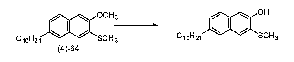
6-デシル-3-メチルチオ-2-メトキシナフタレン(化合物(4)-64)(28g,81mmol)のジクロロメタン(50ml)溶液をBBr3(ca.2M70ml,140mmol)のジクロロメタン溶液に-78℃で加えた。12時間室温で攪拌し、混合物に氷(約20g)を加えた。反応液をジクロロメタン(20ml×3)で抽出した。3回の抽出により得られた有機層を合わせて、飽和食塩水(30ml×3)で洗浄し、MgSO4で乾燥し、濃縮した。残渣をカラムクロマトグラフィー(シリカゲル、ジクロロメタン:ヘキサン=1:1で展開)により精製し、ヘキサンより再結晶し6-デシル-3-メチルチオ-2-ヒドロキシナフタレン(18.1g,72%)を白色結晶として得た。
mp 65.5~66.0 ℃; 1H NMR (270 MHz, CDCl3) δ0.88 (t, J = 6.7 Hz, 3H), 1.26-1.32(m, 14H), 1.67 (quint, J= 7.7 Hz, 2H), 2.41 (s, 3H), 2.71 (t, J = 7.3 Hz, 2H), 6.57 (s, 1H), 7.28 (s, 1H), 7.28 (dd, J = 8.2 Hz, 1.6 Hz, 1H), 7.48 (brs, 1H), 7.61 (d, J = 8.6 Hz, 1H), 7.94 (s, 1H); 13C NMR (100 MHz, CDCl3) δ14.1, 19.9, 22.7, 29.3, 29.6 (×3), 31.4, 31.9, 35.9, 109.1, 124.1, 125.7, 126.3, 128.7, 129.1, 133.5 (×2), 138.5, 152.1; IR (KBr) ν3402 cm-1(OH); EIMS (70 eV) m/z = 330 (M+); Anal. Calcd for C21H30OS: C, 76.31; H, 9.15%. Found: C, 76.34; H, 9.23%.

得られた6-デシル-3-メチルチオ-2-ヒドロキシナフタレン(3.63g,10mmol)とピリジン(2.5ml,30mmol)とのジクロロメタン(50ml)溶液にトリフルオロメタンスルホン酸無水物(3ml,15mmol)を0℃で加えた。これを25分間室温で攪拌したのち、混合物を水(20ml)で希釈し塩酸(4M,20ml)を加えた。この混合物をジクロロメタン(30ml×3)で抽出した。3回の抽出により得られた有機層を合わせ、飽和食塩水(30ml×3)で洗浄し、MgSO4で乾燥し濃縮して6-デシル-3-メチルチオ-2-(トリフルオロメタンスルフォニルオキシ)ナフタレン(化合物(4)-81)(4.89g,99%)を得た。
mp 42.0~42.9℃; 1H NMR (270 MHz, CDCl3) δ0.88 (t, J = 6.7 Hz, 3H), 1.26-1.32(m, 14H), 1.68 (quint, J= 7.7 Hz, 2H), 2.59 (s, 3H), 2.76 (t, J = 7.3 Hz, 2H), 7.36 (dd, J = 8.7 Hz, 1.8 Hz, 1H), 7.57 (brs, 1H), 7.63 (s, 1H), 7.68 (s, 1H), 7.72 (d, J = 8.2 Hz, 1H); 13C NMR (100 MHz, CDCl3) δ14.1, 15.8, 22.7, 29.3 (×2), 29.5, 29.6 (×2), 31.2, 31.9, 36.1, 118.7 (q, J = 319 Hz), 119.2, 125.2, 126.3, 127.7, 128.4, 129.4, 130.7, 133.0, 142.7, 144.8; IR (KBr) ν1423, 1211 cm-1 (-O-SO2-); EIMS (70 eV) m/z = 462 (M+); Anal. Calcd for C22H29F3O3S2: C, 57.12; H, 6.32%. Found C, 56.91; H, 6.15%.
実施例15で合成した7-デシル-3-メチルチオ-2-メトキシナフタレン(化合物(4)-12)を、(合成例1-1)の操作で脱メチル化し、7-デシル-3-メチルチオ-2-ヒドロキシナフタレンを得た。
収率85%;黄色結晶(ヘキサン再結晶);
mp 64.4~65.4℃; 1H NMR (400 MHz, CDCl3) δ0.88 (t, J = 6.9 Hz, 3H), 1.24-1.72 (m, 16H), 2.40 (s, 3H), 2.72 (t, J = 7.7 Hz, 2H), 6.63 (s, 1H), 7.17 (dd, J = 8.4, 1.6 Hz, 1H), 7.45 (s, 1H), 7.63 (d, J = 8.4 Hz, 1H), 7.97 (s, 1H); 13C NMR (100 MHz, CDCl3) δ14.4, 20.4, 23.0, 29.6, 29.7, 29.9 (×2), 31.6, 32.2, 36.5, 109.1, 123.4, 125.2, 125.9, 127.5, 127.8, 134.5, 135.8, 142.3, 153.2; IR (KBr) ν3402 cm-1 (OH); EI-MS, m/z = 330 (M+); Anal. Calcd for C21H30OS: C, 76.31; H, 9.15%. Found: C, 76.62; H, 9.38%.
(合成例1-2)における操作と同様の操作で7-デシル-3-メチルチオ-2-ヒドロキシナフタレンをトリフルオロメタンスルホニル化し、7-デシル-3-メチルチオ-2-(トリフルオロメタンスルホニルオキシ)ナフタレン(化合物(4)-77)を得た。
収率94%;黄色結晶(ヘキサン再結晶);
mp 149~150℃; 1H NMR (400 MHz, CDCl3) δ2.44 (s, 3H), 6.64 (s, 1H), 7.38-7.40 (m, 2H), 7.48 (tt, J = 7.6, 1.8 Hz, 1H), 7.60 (d, J = 8.5 Hz, 1H), 7.70-7.72 (m, 2H), 7.80 (dd, J = 8.5, 2.0 Hz, 1H), 7.88 (s, 1H), 8.02 (d, J = 2.0 Hz, 1H); 13C NMR (126 MHz, CDCl3) δ14.4, 16.4, 23.0, 29.6, 29.7, 29.8, 29.9, 30.0, 31.5, 32.2, 36.3, 119.0 (q, J = 320 Hz), 119.3, 126.6, 127.0, 127.5, 129.7, 129.9, 131.6, 131.8, 142.1, 125.9; IR (neat) ν1427, 1213 cm-1 (-O-SO2-); EI-MS, m/z =266 (M+); Anal. Calcd for C17H14OS: C, 76.66; H, 5.30%. Found: C, 76.97; H, 5.14%.
実施例16で合成した3-メチルチオ-7-フェニル-2-メトキシナフタレン(化合物(4)-22)を(合成例1-1)の操作で脱メチル化し、3-メチルチオ-7-フェニル-2-ナフトールを得た。
収率94%;黄色結晶(ヘキサン再結晶);
mp 149~150℃; 1H NMR (400 MHz, CDCl3) δ2.44 (s, 3H), 6.64 (s, 1H), 7.38-7.40 (m, 2H), 7.48 (tt, J = 7.6, 1.8 Hz, 1H), 7.60 (d, J = 8.5 Hz, 1H), 7.70-7.72 (m, 2H), 7.80 (dd, J = 8.5, 2.0 Hz, 1H), 7.88 (s, 1H), 8.02 (d, J = 2.0 Hz, 1H); 13C NMR (100 MHz, CDCl3) δ20.2, 109.8, 124.1, 124.7, 127.7, 127.9, 128.5, 129.2 (×2), 134.1, 135.7, 140.1, 141.3, 153.4; IR (KBr) ν3497 cm-1 (OH); EI-MS, m/z = 266 (M+); Anal. Calcd for C17H14OS: C, 76.66; H, 5.30%. Found: C, 76.97; H,5.14%.
(合成例1-2)における操作と同様の操作で3-メチルチオ-7-フェニル-2-ナフトールをトリフルオロメタンスルホニル化し、3-メチルチオ-7-フェニル-2-(トリフルオロメタンスルホニルオキシ)ナフタレン(化合物(4)-72)を得た。
収率98%;黄色結晶(ヘキサン再結晶);
mp 87.8~88.7℃; 1H NMR (400 MHz, CDCl3) δ2.62 (s, 3H), 7.41 (tt, J = 7.2, 1.2 Hz, 1H), 7.45-7.52 (m, 2H), 7.68-7.71 (m, 2H), 7.72 (s, 1H), 7.79 (s, 1H), 7.82 (dd, J = 8.4, 1.6 Hz, 1H), 7.87 (d, J = 8.4 Hz, 1H), 8.00 (s, 1H); 13C NMR (126 MHz, CDCl3) δ16.0, 119.0 (q, J = 321 Hz), 120.0, 125.9, 126.8, 127.6, 127.7, 127.8, 128.2, 129.3, 131.3, 131.7, 132.3, 139.8, 140.5, 146.0; IR (KBr) ν1425, 1209 cm-1(O-SO2-); EI-MS, m/z = 398 (M+); Anal. Calcd for C18H13O3S2F3: C, 54.26; H, 3.29%. Found: C, 54.42; H, 3.08%.
(合成例4-1):3-メチルチオ-6-フェニル-2-ナフトールの合成
実施例17で合成した3-メチルチオ-6-フェニル-2-メトキシナフタレン(化合物(4)-31)を、(合成例1-1)の操作で脱メチル化し、3-メチルチオ-6-フェニル-2-ナフトールを得た。
収率73%;黄色結晶(ヘキサン再結晶);
mp 128.9~129.8℃; 1H NMR (400 MHz, CDCl3) δ2.45 (s, 3H), 6.63 (s, 1H), 7.35 (s, 1H), 7.37 (tt, J = 7.4, 1.3 Hz, 1H), 7.45-7.50 (m, 2H), 7.72 (dd, J = 8.5, 1.8 Hz, 1H), 7.76 (d, J = 8.6 Hz, 1H) 7.68-7.72 (m, 2H), 7.76 (d, J = 8.5 Hz, 1H), 7.92 (d, J = 1.8 Hz, 1H); 13C NMR (100 MHz, CDCl3) δ20.2, 109.4, 125.2, 125.5, 127.1, 127.3, 127.5, 127.6, 129.2, 129.5, 134.5 (×2), 137.0, 141.3, 153.1; IR (KBr) ν3402 cm-1 (OH); EI-MS, m/z = 266 (M+); Anal. Calcd for C17H14OS: C, 76.66; H, 5.30%. Found: C, 76.50; H, 5.15%.
(合成例1-2)の操作と同様の操作で3-メチルチオ-6-フェニル-2-ナフトールをトリフルオロメタンスルホニル化し、3-メチルチオ-6-フェニル-2-(トリフルオロメタンスルホニルオキシ)ナフタレン(化合物(4)-73)を得た。
収率 定量的;黄色結晶(ヘキサン再結晶);
mp 79.4~80.3℃; 1H NMR (400 MHz, CDCl3) δ2.62 (s, 3H), 7.42 (tt, J = 7.4, 1.3Hz, 1H), 7.43-7.52 (m, 2H), 7.68-7.71 (m, 2H), 7.74 (s, 1H), 7.75 (s, 1H), 7.77 (dd, J = 8.5, 1.8 Hz, 1H), 7.88 (d, J = 8.5 Hz, 1H), 7.99 (d, J = 1.8 Hz, 1H); 13C NMR (126 MHz, CDCl3) δ16.0, 119.0 (q, J = 321 Hz), 119.6, 124.9, 126.8, 127.1, 127.8, 128.2, 128.7, 129.3, 130.5, 131.9, 133.4, 140.7, 140.9, 145.6; IR (KBr) ν1429, 1225 cm-1(O-SO2-); EI-MS, m/z = 398 (M+); Anal. Calcd for C18H13O3S2F3: C, 54.26; H, 3.29%. Found: C, 54.17; H, 3.01%.
(合成例1-1)と同様の方法で、実施例18で得られた6-トリル-3-メチルチオ-2-メトキシナフタレン(化合物(4)-32,10.5g)をBBr3のジクロロメタン溶液で脱メチル化し、その後、CF3SO2化して、6-トリル-3-メチルチオ-2-トリフルオロメタンスルフォニルオキシナフタレンの合成(化合物(4)-83,12.5g,収率85%)を得た。
EI-MS, m/z=412(M+)
(合成例1-1)と同様の方法で、実施例19で得られた7-トリル-3-メチルチオ-2-メトキシナフタレン(化合物(4)-23,15.4g)をBBr3のジクロロメタン溶液で脱メチル化し、その後、CF3SO2化して、7-トリル-3-メチルチオ-2-トリフルオロメタンスルフォニルオキシナフタレン(化合物(4)-82,8.62g,収率67%)を得た。
EI-MS, m/z=412(M+)
(合成例1-1)と同様の方法で、実施例20で得られた6-ビフェニル-3-メチルチオ-2-メトキシナフタレンの合成(化合物(4)-33,15.4g)をBBr3のジクロロメタン溶液で脱メチル化し、その後、CF3SO2化して、6-ビフェニル-3-メチルチオ-2-トリフルオロメタンスルフォニルオキシナフタレン(化合物(4)-85,15.9g,収率77%)を得た。
EI-MS, m/z=474(M+)
(合成例1-1)と同様の方法で、実施例21で得られた7-ビフェニル-3-メチルチオ-2-メトキシナフタレンの合成(化合物(4)-24,15.8g)をBBr3のジクロロメタン溶液で脱メチル化し、その後、CF3SO2化して、7-ビフェニル-3-メチルチオ-2-トリフルオロメタンスルフォニルオキシナフタレン(化合物(4)-84,18.9g,収率93%)を得た。
EI-MS, m/z=474(M+)
(合成例1-1)と同様の方法で、実施例22で得られた7-ブチル-3-メチルチオ-2-メトキシナフタレン(化合物(4)-04,21.63g,83.1mmol)をBBr3のジクロロメタン溶液で脱メチル化し、その後、CF3SO2化して、7-ブチル-3-メチルチオ-2-トリフルオロメタンスルフォニルオキシナフタレン(化合物(4)-74,18.5g,収率59%)を得た。
EI-MS, m/z=378(M+)
(合成例1-1)と同様の方法で、実施例23で得られた7-ヘキシル-3-メチルチオ-2-メトキシナフタレン(化合物(4)-08,24.7g)をBBr3のジクロロメタン溶液で脱メチル化し、その後、CF3SO2化して、7-ヘキシル-3-メチルチオ-2-トリフルオロメタンスルフォニルオキシナフタレン(化合物(4)-75,23.5g,収率70%)を得た。
EI-MS, m/z=406(M+)
(合成例1-1)と同様の方法で、実施例24で得られた7-オクチル-3-メチルチオ-2-メトキシナフタレン(化合物(4)-10,27.09g)をBBr3のジクロロメタン溶液で脱メチル化し、その後、CF3SO2化して、7-オクチル-3-メチルチオ-2-トリフルオロメタンスルフォニルオキシナフタレン(化合物(4)-76,25.00g,収率64%)を得た。
EI-MS, m/z=434(M+)
(合成例1-1)と同様の方法で、実施例25で得られた7-ドデシル-3-メチルチオ-2-メトキシナフタレンの合成(化合物(4)-14,34.1g)をBBr3のジクロロメタン溶液で脱メチル化し、その後、CF3SO2化して、7-ドデシル-3-メチルチオ-2-トリフルオロメタンスルフォニルオキシナフタレン(化合物(4)-78,33.7g,収率72%)を得た。
EI-MS, m/z=490(M+)

窒素雰囲気下、18w%Naアセチレンのキシレンと、ミネラルオイルのディスパージョンオイル(10ml,8.5g,32mmol)とのTHF(60ml)溶液にトリブチルチンクロリド(8.6ml,32mmol)を0℃で加えた。17時間室温で攪拌した後、混合物をヘキサンで抽出し食塩水で洗浄した。有機層を混合しMgSO4で乾燥したのち濃縮した。減圧蒸留(85~120℃,約0.7mmHg)して、トリブチルスタニルアセチレン(3.6g,34%)を無色油状物質として得た。
1H-NMR (400 MHz, CDCl3) δ0.91 (t, 9H, J = 8.0 Hz), 1.02 (t, 8H, J = 8.0 Hz), 1.35 (sextet, 6H, J = 8.0 Hz), 1.58 (quintet, 6H, J = 8.0 Hz), 2.20 (s,1H)

窒素雰囲気下、トリブチルスタニルアセチレン(1.6g,5mmol)と、トリブチルチンハイドライド(1.3ml,5mmol)とのトルエン(20ml)溶液にアゾビスイソブチロニトリル(100mg,0.60mmol)を加えた。この混合物を17時間、90℃で加熱攪拌し、水(20ml)を加えたのち濃縮した。混合物をヘキサンで抽出し、抽出液を食塩水で洗浄して1,2-ビス(トリブチルスタニル)エチレン(化合物(5)-05)(3.0g,90%)を無色油状物質として得た。
1H-NMR (400 MHz, CDCl3) δ0.86-0.91 (multiplet, 15H), 1.31 (sextet, 6H, J = 8.0Hz), 1.50 (quintet,6H, J = 8.0 Hz), 6.88 (s,2H)

6-デシル-3-メチルチオ-2-(トリフルオロメタンスルフォニルオキシ)ナフタレン(化合物(4)-81)(1.9g,4.1mmol)と、1,2-ビス(トリブチルスタニル)エチレン(化合物(5)-05)とのDMF(40ml)溶液に、Pd(PPh3)4(322mg,0.29mmol,7mol%)を加えた。混合物を暗所、90℃で17時間加熱攪拌し、水で希釈しクロロホルムで抽出した。この抽出液をMgSO4で乾燥して濃縮した。残渣をカラムクロマトグラフィー(シリカゲル、ジクロロメタンで展開)により精製し、トランス-1,2-ビス(6-デシル-3-メチルチオナフタレン-2-イル)エチレン(化合物(6)-64)(2.3g,定量的)を黄色固体として得た。
mp 116.8~117.7℃; 1H NMR (400 MHz, CDCl3) δ0.88 (t, J = 6.4 Hz, 6H), 1.29-1.70 (m, 32H), 2.58 (s, 6H), 2.75 (t, J = 8.4 Hz, 4H), 7.29 (dd, J = 8.8, 1.6 Hz, 2H), 7.52 (s, 2H), 7.59 (s, 2H), 7.64 (s, 2H), 7.76 (d, J = 8.4 Hz, 2H), 8.06 (s, 2H); 13C NMR (100 MHz, CDCl3) δ14.4, 16.8, 23.0, 24.2, 29.6, 29.8, 29.9, 30.0, 31.7, 32.2, 36.5, 124.3, 125.2, 125.3, 127.6, 128.0, 128.4, 130.3, 133.9, 134.5, 136.0, 141.6; EI-MS m/z = 652 (M+).
実施例26と同様の操作で7-デシル-3-メチルチオ-2-(トリフルオロメタンスルフォニルオキシ)ナフタレン(化合物(4)-77)及び1,2-ビス(トリブチルスタニル)エチレン(化合物(5)-05)から、trans-1,2-ビス(7-デシル-3-メチルチオナフタレン-2-イル)エチレン(化合物(6)-12)を得た。
収率98%;黄色結晶(再結晶ヘキサン);
mp 87.8-88.7℃; 1H NMR (400 MHz, CDCl3) δ 2.62 (s, 3H), 7.41 (tt, J = 7.2, 1.2Hz, 1H), 7.45-7.52 (m, 2H), 7.68-7.71 (m, 2H), 7.72 (s, 1H), 7.79 (s, 1H), 7.82 (dd, J= 8.4, 1.6 Hz, 1H), 7.87 (d, J= 8.4 Hz, 1H), 8.00 (s, 1H); EI-MS, m/z = 398 (M+); Anal. Calcd for C18H13O3S2F3: C, 54.26; H, 3.29%. Found: C, 54.42; H, 3.08%.
実施例26と同様の操作で3-メチルチオ-7-フェニル-2-(トリフルオロメタンスルホニルオキシ)ナフタレン(化合物(4)-72)と、1,2-ビス(トリブチルスタニル)エチレン(化合物(5)-05)とから、trans-1,2-ビス(3-メチルチオ-7-フェニルナフト-2-イル)エチレン(化合物(6)-22)を得た。
収率63%;黄色固体(再結晶ヘキサン);
mp 87.8~88.7℃; 1H NMR (400 MHz, CDCl3) δ2.63 (s, 6H), 7.40 (tt, J = 7.4, 1.2 Hz, 2H), 7.48-7.52 (m, 4H), 7.68 (s, 2H), 7.73-7.76 (m, 4H), 7.72 (s, 2H), 7.72 (d, J = 8.2 Hz, 2H), 7.83 (d, J = 8.2 Hz, 2H), 8.08 (s, 2H), 8.17 (s, 2H); EI-MS, m/z = 524 (M+); Anal. Calcd for C34H25S2: C, 82.40; H, 5.38%. Found: C, 82.38; H, 5.22%.
実施例26と同様の操作で3-メチルチオ-6-フェニル-2-(トリフルオロメタンスルホニルオキシ)ナフタレン(化合物(4)-73)と、1,2-ビス(トリブチルスタニル)エチレン(化合物(5)-05)とから、trans-1,2-ビス(3-メチルチオ-6-フェニルナフト-2-イル)エチレン(化合物(6)-31)を得た。
収率57%;黄色固体(再結晶ヘキサン);
mp 191.5~192.4℃; 1H NMR (400 MHz, CDCl3) δ2.64 (s, 6H), 7.40 (tt, J = 7.2, 1.6 Hz, 2H), 7.48-7.53 (m, 4H), 7.71 (s, 2H), 7.72 (s, 2H), 7.73-7.76 (m, 4H), 7.76 (d, J = 8.7 Hz, 2H), 7.94 (d, J = 8.7 Hz, 2H), 7.97 (s, 2H), 8.14 (s, 2H); EI-MS, m/z = 524 (M+); Anal. Calcd for C34H25S2: C, 82.40; H, 5.38%. Found: C, 82.22; H, 5.29%.
実施例26と同様の操作で、6-トリル-3-メチルチオ-2-トリフルオロメタンスルフォニルオキシナフタレンの合成(化合物(4)-83,12.5g)から、trans-1,2-ビス(6-トリル-3-メチルチオナフタレン-2-イル)エチレン(化合物(6)-32,2.0g,収率24%)を淡黄色固体で得た。
EI-MS, m/z=552(M+)
実施例26と同様の操作で、7-トリル-3-メチルチオ-2-トリフルオロメタンスルフォニルオキシナフタレン(化合物(4)-82,8.50g)から、trans-1,2-ビス(7-トリル-3-メチルチオナフタレン-2-イル)エチレン(化合物(6)-23,3.64g,収率64%)を淡黄色固体で得た。
EI-MS, m/z=552(M+)
実施例26と同様の操作で、6-ビフェニル-3-メチルチオ-2-トリフルオロメタンスルフォニルオキシナフタレン(化合物(4)-85,15.8g)から、trans-1,2-ビス(6-ビフェニル-3-メチルチオナフタレン-2-イル)エチレン(化合物(6)-33,8.52g,収率76%)を淡黄色固体で得た。
EI-MS, m/z=676(M+)
実施例26と同様の操作で、7-ビフェニル-3-メチルチオ-2-トリフルオロメタンスルフォニルオキシナフタレン(化合物(4)-84,18.9g)から、trans-1,2-ビス(7-ビフェニル-3-メチルチオナフタレン-2-イル)エチレン(化合物(6)-24,11.56g,収率86%)を淡黄色固体で得た。
EI-MS, m/z=676(M+)
実施例26と同様の操作で、7-ブチル-3-メチルチオ-2-トリフルオロメタンスルフォニルオキシナフタレン(化合物(4)-74,18.20g,47.6mmol)から、trans-1,2-ビス(7-ブチル-3-メチルチオナフタレン-2-イル)エチレン(化合物(6)-04)を淡黄色固体(5.32g,収率45%)で得た。
EI-MS, m/z=492(M+)
実施例26と同様の操作で、7-ヘキシル-3-メチルチオ-2-トリフルオロメタンスルフォニルオキシナフタレン(化合物(4)-75,23.3g)から、trans-1,2-ビス(7-ヘキシル-3-メチルチオナフタレン-2-イル)エチレン(化合物(6)-08)を淡黄色固体(6.73g,収率43%)で得た。
EI-MS, m/z=540(M+)
実施例26と同様の操作で、7-オクチル-3-メチルチオ-2-トリフルオロメタンスルフォニルオキシナフタレン(化合物(4)-76,25.00g)から、trans-1,2-ビス(7-オクチル-3-メチルチオナフタレン-2-イル)エチレン(化合物(6)-10)を淡黄色固体(7.46g,収率43%)で得た。
EI-MS, m/z=596(M+)
実施例26と同様の操作で、7-オクチル-3-メチルチオ-2-トリフルオロメタンスルフォニルオキシナフタレンの合成(化合物(4)-78,27.8g)から、trans-1,2-ビス(7-ドデシル-3-メチルチオナフタレン-2-イル)エチレン(化合物(6)-14)を淡黄色固体(8.08g,収率40%)で得た。
EI-MS, m/z=709(M+)

trans-1,2-ビス(6-デシル-3-メチルチオナフタレン-2-イル)エチレン(化合物(6)-64)(38mg,58mmol)とI2(470mg,1.8mmol)とのクロロホルム(4ml)溶液を20時間室温で攪拌した。この混合物を濃縮し、メタノール(5ml)とNaHSO3水溶液(5ml)とを加えた。ろ別してから、水、アセトン、メタノール、及びトルエンで洗浄し、2,9-ジデシルジナフト[2,3-b:2’,3’-f]チエノ[2,3-b]チオフェン(化合物(2)-64)(29mg,81%)を黄色固体として得た。
EIMS (70 eV) m/z = 620 (M+).
合成例14と同様の方法で、trans-1,2-ビス(7-デシル-3-メチルチオナフタレン-2-イル)エチレン(化合物(6)-12)から、3,10-ジデシルジナフト[2,3-b:2’,3’-f]チエノ[2,3-b]チオフェン(化合物(1)-12)を得た。
収率71%;mp 187~188℃;
1H NMR (400 MHz, CDCl3) δ0.88 (t, J = 6.9 Hz, 6H), 1.24-1.79 (m, 32H), 2.82 (t, J = 7.7 Hz, 4H), 7.38 (dd, J = 8.5, 1.6 Hz, 2H), 7.79 (s, 2H), 7.86 (d, J = 8.5 Hz, 2H), 8.29 (s, 2H), 8.36 (s, 2H); EI-MS, m/z = 620 (M+); Anal. Calcd for C42H52S2: C, 81.46; H, 8.43%. Found: C, 81.13; H, 8.43%.
合成例14と同様の方法で、trans-1,2-ビス(3-メチルチオ-7-フェニルナフト-2-イル)エチレン(化合物(6)-22)から、3,10-ジフェニルジナフト[2,3-b:2’,3’-f]チエノ[3,2-b]チオフェン(3,10-PhDNTT)(化合物(1)-22)を得た。
収率85%;mp>300℃;
EI-MS, m/z = 492 (M+); Anal. Calcd for C34H20S2: C, 82.89 H, 4.09%. Found: C, 82.80 H 3.78%.
合成例14と同様の方法で、trans-1,2-ビス(3-メチルチオ-6-フェニルナフト-2-イル)エチレン(化合物(6)-31)から、2,9-ジフェニルジナフト[2,3-b:2’,3’-f]チエノ[3,2-b]チオフェン(2,9-PhDNTT)(化合物(1)-31)を得た。
収率89%;mp>300℃;
EI-MS, m/z = 492 (M+); Anal. Calcd for C34H20S2: C, 82.89 H, 4.09%. Found: C, 82.73 H, 3.75%.
合成例14と同様の方法で、trans-1,2-ビス(6-トリル-3-メチルチオナフタレン-2-イル)エチレンの合成(化合物(6)-32,2.0g)から、2,9-ジトリルジナフト[2,3-b:2’,3’-f]チエノ[2,3-b]チオフェン(化合物(1)-32)を黄色固体(1.78g,95%)で得た。
EI-MS, m/z=520(M+),427,260(M+/2)。
熱分析(吸熱ピーク):492℃(TG-DTA使用、窒素)
合成例14と同様の方法で、trans-1,2-ビス(7-トリル-3-メチルチオナフタレン-2-イル)エチレン(化合物(6)-23,3.60g)から、3,10-ジトリルジナフト[2,3-b:2’,3’-f]チエノ[2,3-b]チオフェン(化合物(1)-23)を黄色固体(3.38g,定量的)で得た。
EI-MS, m/z=520(M+),427,260(M+/2),172.
熱分析(吸熱ピーク):401℃(TG-DTA使用、窒素)
合成例14と同様の方法で、trans-1,2-ビス(6-ビフェニル-3-メチルチオナフタレン-2-イル)エチレンの合成(化合物(6)-33,8.40g)をヨウ素と反応させ、2,9-ジビフェニルジナフト[2,3-b:2’,3’-f]チエノ[2,3-b]チオフェン(化合物(1)-33)を黄色固体(7.76g,97%)で得た。
EI-MS, m/z=644(M+),566,490,429,322(M+/2),207.
熱分析(吸熱ピーク)500℃まで明確なピークなし(TG-DTA使用、窒素)
合成例14と同様の方法で、trans-1,2-ビス(7-ビフェニル-3-メチルチオナフタレン-2-イル)エチレン(化合物(6)-24,11.50g)をヨウ素と反応させ、3,10-ジビフェニルジナフト[2,3-b:2’,3’-f]チエノ[2,3-b]チオフェン(化合物(1)-24)を黄色固体(10.32g,収率94%)で得た。
EI-MS, m/z=644(M+),492,429,322(M+/2),270.
熱分析(吸熱ピーク):500℃まで明確なピークなし(TG-DTA使用、窒素)
合成例14と同様の方法で、trans-1,2-ビス(7-ブチル-3-メチルチオナフタレン-2-イル)エチレン(化合物(6)-04)をヨウ素と反応させ、3,10-ジブチルジナフト[2,3-b:2’,3’-f]チエノ[2,3-b]チオフェン(化合物(1)-04)を黄色固体(4.66g,定量的)で得た。
EI-MS, m/z=452(M+),409,366,184,183.
熱分析(吸熱ピーク):185,283℃(DSC使用、窒素)
1H NMR (400 MHz, CDCl3) δ0.98 (t, 6H), δ1.35~1.50 (m, 4H), δ1.70-1.80 (m, 4H),δ2.80-2.90 (m, 4H) δ7.39 (dd, 2H, ArH) δ7.78 (s, 2H, ArH) δ7.84 (d, 2H, ArH) δ8.27 (s, 2H, ArH) δ8.34 (s, 2H, ArH) 。
合成例14と同様の方法で、trans-1,2-ビス(7-ヘキシル-3-メチルチオナフタレン-2-イル)エチレン(化合物(6)-08,6.50g)をヨウ素と反応させ、3,10-ジヘキシルジナフト[2,3-b:2’,3’-f]チエノ[2,3-b]チオフェン(化合物(1)-08)を黄色固体(3.18g,収率52%)で得た。
EI-MS, m/z=508(M+),437,366,184,183
熱分析(吸熱ピーク):202,259℃(DSC使用、窒素)
1H NMR (400 MHz, CDCl3) δ0.90 (t, 6H), δ1.20~1.55 (m, 12H), δ1.70-1.80 (m, 4H), δ2.75-2.90 (m, 4H) δ7.39 (dd, 2H, ArH) δ7.78 (s, 2H, ArH) δ7.84 (d, 2H, ArH) δ8.27 (s, 2H, ArH) δ8.34 (s, 2H, ArH) 。
合成例14と同様の方法で、trans-1,2-ビス(7-ヘキシル-3-メチルチオナフタレン-2-イル)エチレン(化合物(6)-10,7.20g,12.1mmol)をヨウ素と反応させ、3,10-ジオクチルジナフト[2,3-b:2’,3’-f]チエノ[2,3-b]チオフェン(化合物(1)-10)を黄色固体(3.50g,収率51%)で得た。
EI-MS, m/z=564(M+),465,366,184,183
熱分析(吸熱ピーク):177,237℃(DSC使用、窒素)
1H NMR (400 MHz, CDCl3) δ0.88 (m, 6H), δ1.10~1.50 (m, 20H), δ1.60-1.85 (m, 4H), δ2.70-2.90 (m, 4H) δ7.36 (m, 2H, ArH) δ7.77 (s, 2H, ArH) δ7.83 (d, 2H, ArH) δ8.26 (s, 2H, ArH) δ8.30 (s, 2H, ArH) 。
合成例14と同様の方法で、trans-1,2-ビス(7-ドデシル-3-メチルチオナフタレン-2-イル)エチレン(化合物(6)-14,7.80,11mmol)をヨウ素と反応させ、3,10-ジドデシルジナフト[2,3-b:2’,3’-f]チエノ[2,3-b]チオフェン(化合物(1)-14)を黄色固体(6.26g,収率84%)で得た。
EI-MS, m/z=677(M+),521,366,184,183
熱分析(吸熱ピーク):100,123,158,212℃(DSC使用、窒素)
1H NMR (400 MHz, CDCl3) δ0.80-0.90 (m, 6H), δ1.20~1.60 (m, 36H), δ1.70-1.85 (m, 4H), δ2.80-2.90 (m, 4H) δ7.36 (dd, 2H, ArH) δ7.80 (s, 2H, ArH) δ7.83 (d, 2H, ArH) δ8.26 (s, 2H, ArH) δ8.34 (s, 2H, ArH) 。
オクタデシルトリクロロシラン処理を行った300nmのSiO2熱酸化膜付きnドープシリコンウェハー(面抵抗0.02Ω・cm以下)を真空蒸着装置内に設置し、装置内の真空度が5.0×10⁻³Pa以下になるまで排気した。抵抗加熱蒸着法によって、この電極に基板温度約60℃の条件下、化合物(1)-12、(1)-22及び(1)-31をそれぞれ50nmの厚さに蒸着し、半導体層(2)を形成した。次いでこの基板に電極作製用シャドウマスクを取り付け、真空蒸着装置内に設置し、装置内の真空度が1.0×10⁻⁴Pa以下になるまで排気し、抵抗加熱蒸着法によって、金の電極、すなわちソース電極(1)及びドレイン電極(3)を40nmの厚さに蒸着し、TC(トップコンタクト)型である本発明の電界効果トランジスタを得た。
得られた電界効果トランジスタをプローバー内に設置し半導体パラメーターアナライザー4155C(Agilent社製)を用いて半導体特性を測定した。半導体特性はゲート電圧を10V~-100Vまで20Vステップで走査し、またドレイン電圧を10V~-100Vまで走査し、ドレイン電流-ドレイン電圧を測定した。その結果、電流飽和が観測され、得られた電圧電流曲線より、本素子はp型半導体を示し、算出したキャリア移動度を表7に示した。
実施例49で用いた本願実施化合物の代わりにDNTT(Ref-01)、3,10-DM-DNTT(Ref-02;(1)におけるR1がメチル基の化合物)及び2,9-DM-DNTT(Ref-03;(1)におけるR2がメチル基の化合物)を用いて、実施例49と同様の操作により、TC型の電界効果トランジスタを得た。使用した化合物、及びその結果を表7に示した。
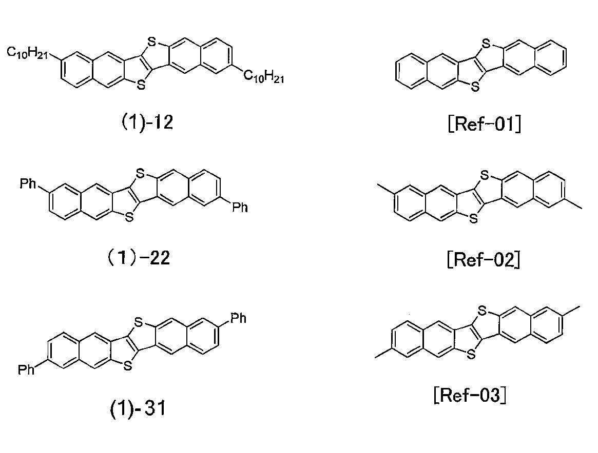

実施例38から実施例48で合成した本願化合物及び比較例1のRef-01化合物、化合物(2)-64を用いて、HMDS-SAMにより処理基板を用いて蒸着時基板温度を25℃及び100℃,L=50μm,W=2000μmとした以外は実施例49と同様の操作にてTC型の電界効果トランジスタを作製した。得られたトランジスタの半導体特性を実施例49に倣って測定し、算出したキャリア移動度を表8に示した。これらの結果から本願化合物はいずれもp型半導体材料としての高い性能を示すことがわかった。

実施例51
実施例39で合成した化合物(1)-22及び合成例14で合成した化合物(2)-64を用いて、HMDS-SAMにより処理基板を用いて蒸着時基板温度100℃,L=40μm,W=1500μmとした以外は実施例49と同様の操作により、TC型の電界効果トランジスタを作製し、耐熱性試験を行った。測定結果を表9に示した。初期特性(μ=1.66cm2/Vs,Vth=-14V,Ion/off~109)と比較して、100℃、および150℃でのアニール後でも移動度は、~1.6cm2/Vsであり、初期値とほぼ同程度を維持し、Vthは、低電位側にシフトするなど特性が向上していた。それに対して、化合物(2)-64では120℃程度で移動度が半減した。これらの実験から、本発明である化合物(1)-22などのアリール基が置換する化合物では、高い熱的安定性をもち、工業的プロセスにも耐え得るトランジスタを実現することが可能であることが確認できた。

2,9位にC10アルキル基を有するDNTT(化合物(2)-64)や3,10位にC10アルキル基を有するDNTT(化合物(1)-12)等をクロロホルムに溶解して得られる飽和溶液の吸収スペクトルを図4に示す。C10の長鎖アルキル基を有するDNTTは置換位置による最長吸収波長における相対強度から、2,9-C10-DNTT(化合物(2)-64)を1とした場合、結果より、3,10-C10-DNTT(化合物(1)-12)は3.9であり、置換位置の違いにより高い溶解性を示すことが判明した。また、トルエン中、60℃での溶解度は、2,9-C10-DNTT(化合物(2)-64)は45mg/L、3,10-C10-DNTT(化合物(1)-09)は>260mg/Lとなり、加温状態においても、3,10-C10-DNTT(化合物(1)-12)の溶解性の高さが明確に認められた(表10)。

オクタデシルトリクロロシラン処理を行った300nmのSiO2熱酸化膜付きnドープシリコンウェハー(面抵抗0.02Ω・cm以下)を真空蒸着装置内に設置し、装置内の真空度が5.0×10⁻³Pa以下になるまで排気した。抵抗加熱蒸着法によって、この電極に基板温度約100℃の条件下、化合物(1)-12、2-(64)をそれぞれ50nmの厚さに蒸着し、半導体層(2)を形成した。次いでこの基板にチャネル長Lが40μm又は190μmである電極作製用シャドウマスク(チャンネル幅は1500μm)を取り付け、真空蒸着装置内に設置し、装置内の真空度が1.0×10⁻⁴Pa以下になるまで排気し、抵抗加熱蒸着法によって、金の電極、すなわちソース電極(1)及びドレイン電極(3)を40nmの厚さに蒸着し、TC(トップコンタクト)型である本発明の電界効果トランジスタを得た。実施例49と同様にしてこれらの半導体特性を測定した結果を表11に纏めた。3,10位に置換した化合物(1)-12はL=40μmとL=190μmの場合とを比較して、移動度がほとんど低下せず、チャネル長依存性が少ないことを示した。一方で2,9位に置換した化合物(2)-64はL=190μmの時は移動度6.1cm2/Vsのトランジスタを与えるが、チャネル長依存性が顕著であり、L=40μmで移動度が半減以下となった。

1 ソース電極
2 半導体層
3 ドレイン電極
4 絶縁体層
5 ゲート電極
6 基板
7 保護層
Claims (17)
- 下記式(1)で表される複素環式化合物。

(式中、R1及びR2は水素原子、C2-C16アルキル基、又はアリール基のいずれかを表すが、R1がそれぞれ独立にC2-C16アルキル基又はアリール基を表すとき、R2は水素原子又はそれぞれ独立にアリール基を表し、R1が水素原子を表すとき、R2はそれぞれ独立にアリール基を表す。) - 式(1)においてR1がそれぞれ独立に直鎖のC5-C12アルキル基であり、R2は水素原子である請求項1に記載の複素環式化合物。
- 式(1)においてR1がそれぞれ独立にフェニル、ナフチル、ビフェニルのいずれかの骨格を有するアリール基であり、かつR2が水素原子である請求項1に記載の複素環式化合物。
- 式(1)においてR1が水素原子であり、かつR2がそれぞれ独立にフェニル、ナフチル、ビフェニルのいずれかの骨格を有するアリール基である請求項1に記載の複素環式化合物。
- 式(1)においてR1がそれぞれ独立に、フェニル基、4-アルキルフェニル基、1-ナフチル基、及びビフェニル基から選ばれるアリール基であり、かつR2が水素原子である請求項3に記載の複素環式化合物。
- 式(1)においてR1が水素原子であり、かつR2がそれぞれ独立に、フェニル基、4-アルキルフェニル基、1-ナフチル基、及びビフェニル基から選ばれるアリール基である請求項4に記載の複素環式化合物。
- 式(2)で表される複素環式化合物の製造における式(4)で表される中間体化合物の製造方法であって、式(3)で表される化合物とジメチルジスルフィドとを反応させることを含む、中間体化合物(4)の製造方法。

(式中、R3は置換基を表す。)

(式中、R3、R4は置換基を表す。) - 式(2)で表される複素環式化合物の製造における式(6)で表される中間体化合物の製造方法であって、式(4)で表される化合物と式(5)で表されるスズ化合物とを反応させることを含む、中間体化合物(6)の製造方法。


(式中、R3、R4、R5は置換基を表す。) - 請求項1乃至6のいずれか一項に記載の式(1)で表される複素環式化合物を一種又は複数種含む有機半導体材料。
- 請求項1乃至6のいずれか一項に記載の式(1)で表される複素環式化合物を一種又は複数種含有する半導体デバイス作製用インク。
- 請求項1乃至6のいずれか一項に記載の式(1)で表される複素環式化合物の一種又は複数種を含む有機薄膜。
- 請求項11に記載の有機薄膜が蒸着法により形成される有機薄膜の製造方法。
- 請求項11に記載の有機薄膜が請求項10に記載の半導体デバイス作製用インクを塗布することによって形成される有機薄膜の製造方法。
- 請求項11に記載の有機薄膜を有する電界効果トランジスタ。
- ボトムコンタクト型である請求項14に記載の電界効果トランジスタ。
- トップコンタクト型である請求項14に記載の電界効果トランジスタ。
- 請求項1乃至6のいずれか一項に記載の式(1)で表される複素環式化合物の一種又は複数種からなる有機薄膜を請求項12又は請求項13に記載の方法によって基板上に形成する工程を含む電界効果トランジスタの製造方法。
Priority Applications (7)
| Application Number | Priority Date | Filing Date | Title |
|---|---|---|---|
| KR1020147036416A KR101599688B1 (ko) | 2011-02-25 | 2012-02-24 | 신규 헤테로시클릭 화합물, 이를 위한 중간체 제조 방법, 및 이의 용도 |
| KR20137022246A KR20140041439A (ko) | 2011-02-25 | 2012-02-24 | 신규 헤테로시클릭 화합물, 이를 위한 중간체 제조 방법, 및 이의 용도 |
| JP2013501145A JP5674916B2 (ja) | 2011-02-25 | 2012-02-24 | 新規複素環式化合物及びその中間体の製造方法並びにその用途 |
| US14/000,440 US9018630B2 (en) | 2011-02-25 | 2012-02-24 | Heterocyclic dinaphtho thieno thiophene (DNTT) compounds for use as organic semiconductor thin films in field effect transistors and related methods |
| CN201280010570.8A CN103391942B (zh) | 2011-02-25 | 2012-02-24 | 新型杂环化合物、制造其中间体的方法及其用途 |
| KR1020157013064A KR101599687B1 (ko) | 2011-02-25 | 2012-02-24 | 신규 헤테로시클릭 화합물, 이를 위한 중간체 제조 방법, 및 이의 용도 |
| EP12750215.1A EP2679592B1 (en) | 2011-02-25 | 2012-02-24 | Novel heterocyclic compound, method for producing intermediate therefor, and use thereof |
Applications Claiming Priority (2)
| Application Number | Priority Date | Filing Date | Title |
|---|---|---|---|
| JP2011039403 | 2011-02-25 | ||
| JP2011-039403 | 2011-02-25 |
Publications (1)
| Publication Number | Publication Date |
|---|---|
| WO2012115236A1 true WO2012115236A1 (ja) | 2012-08-30 |
Family
ID=46721008
Family Applications (1)
| Application Number | Title | Priority Date | Filing Date |
|---|---|---|---|
| PCT/JP2012/054604 WO2012115236A1 (ja) | 2011-02-25 | 2012-02-24 | 新規複素環式化合物及びその中間体の製造方法並びにその用途 |
Country Status (7)
| Country | Link |
|---|---|
| US (1) | US9018630B2 (ja) |
| EP (2) | EP2679592B1 (ja) |
| JP (2) | JP5674916B2 (ja) |
| KR (3) | KR101599688B1 (ja) |
| CN (2) | CN104650110B (ja) |
| TW (1) | TWI525095B (ja) |
| WO (1) | WO2012115236A1 (ja) |
Cited By (9)
| Publication number | Priority date | Publication date | Assignee | Title |
|---|---|---|---|---|
| WO2014136953A1 (ja) * | 2013-03-08 | 2014-09-12 | 国立大学法人神戸大学 | 有機半導体薄膜の作製方法 |
| CN104956508A (zh) * | 2013-01-22 | 2015-09-30 | 日本化药株式会社 | 溶液工艺用有机半导体材料和有机半导体设备 |
| WO2015147266A1 (ja) * | 2014-03-28 | 2015-10-01 | 富士フイルム株式会社 | 有機半導体膜形成用組成物 |
| WO2016088793A1 (ja) * | 2014-12-05 | 2016-06-09 | 日本化薬株式会社 | 有機化合物及びその用途 |
| JP2017143097A (ja) * | 2016-02-08 | 2017-08-17 | 株式会社デンソー | 有機電界効果トランジスタ |
| JP2018026559A (ja) * | 2016-08-03 | 2018-02-15 | 日本化薬株式会社 | 有機光電変換素子、有機光電変換素子用材料及びこれらを用いた有機撮像素子 |
| KR20180043189A (ko) | 2015-08-28 | 2018-04-27 | 디아이씨 가부시끼가이샤 | 유기 화합물, 그 제조법, 그것을 함유하는 유기 반도체 재료 및 그것을 함유하는 유기 트랜지스터 |
| JP2019206506A (ja) * | 2018-05-29 | 2019-12-05 | Dic株式会社 | 芳香族化合物の製造方法 |
| JP2020189793A (ja) * | 2019-05-21 | 2020-11-26 | 国立大学法人東北大学 | 芳香族化合物の製造方法 |
Families Citing this family (14)
| Publication number | Priority date | Publication date | Assignee | Title |
|---|---|---|---|---|
| EP2402348B1 (en) * | 2009-02-27 | 2017-04-12 | Nippon Kayaku Kabushiki Kaisha | Field effect transistor |
| KR20160011244A (ko) * | 2014-07-14 | 2016-02-01 | 한국과학기술연구원 | 다층 박막의 제조 방법, 이로 인해 형성된 다층 박막, 이를 포함하는 유기 박막 트랜지스터 제조 방법 및 이를 통해 제조된 유기 박막 트랜지스터 |
| CN107360720B (zh) * | 2015-03-23 | 2019-08-02 | 日本化药株式会社 | 有机化合物、有机半导体材料、有机薄膜及制造方法、有机半导体组合物、有机半导体装置 |
| EP3333917B1 (en) * | 2015-08-04 | 2022-04-06 | FUJIFILM Corporation | Organic thin film transistor, method for manufacturing organic thin film transistor, material for organic thin film transistors, composition for organic thin film transistors, organic semiconductor film, and compound |
| US11198698B2 (en) | 2016-02-29 | 2021-12-14 | National Institute Of Advanced Industrial Science And Technology | Organic semiconductor composition, organic thin film comprising same, and use thereof |
| US10056563B2 (en) * | 2016-04-08 | 2018-08-21 | Samsung Electronics Co., Ltd. | Synthetic method of fused heteroaromatic compound and fused heteroaromatic compound, and intermediate thereof |
| TWI734806B (zh) * | 2016-07-19 | 2021-08-01 | 日商日本化藥股份有限公司 | 攝像元件用光電變換元件用材料及含有該材料之光電變換元件 |
| KR20180051260A (ko) | 2016-11-08 | 2018-05-16 | 삼성전자주식회사 | 축합 헤테로방향족 화합물의 합성 방법, 축합 헤테로방향족 화합물 및 그 중간체 및 합성 방법 |
| KR102464890B1 (ko) | 2017-10-18 | 2022-11-07 | 삼성전자주식회사 | 축합다환 헤테로방향족 화합물, 유기 박막 및 전자 소자 |
| KR20200067039A (ko) | 2018-12-03 | 2020-06-11 | 삼성전자주식회사 | 유기 박막, 유기 박막 트랜지스터 및 전자 소자 |
| TW202120513A (zh) * | 2019-09-17 | 2021-06-01 | 日商日本化藥股份有限公司 | 稠合多環芳香族化合物 |
| TW202136272A (zh) | 2019-12-10 | 2021-10-01 | 日商日本化藥股份有限公司 | 縮合多環芳香族化合物 |
| CN112530989B (zh) * | 2020-12-03 | 2024-04-12 | 南京大学 | 一种超高增益有机放大器及其制备方法 |
| CN112531112B (zh) * | 2020-12-03 | 2024-03-22 | 南京大学 | 一种超高增益有机薄膜晶体管及其制备方法 |
Citations (10)
| Publication number | Priority date | Publication date | Assignee | Title |
|---|---|---|---|---|
| JPH06177380A (ja) | 1992-07-30 | 1994-06-24 | Nec Corp | 電界効果型トランジスタおよびその製造方法 |
| JP2001094107A (ja) | 1999-09-20 | 2001-04-06 | Hitachi Ltd | 有機半導体装置及び液晶表示装置 |
| JP2008010541A (ja) | 2006-06-28 | 2008-01-17 | Konica Minolta Holdings Inc | 有機半導体材料、有機半導体膜、有機薄膜トランジスタ及び有機薄膜トランジスタの製造方法 |
| WO2008047896A1 (fr) * | 2006-10-20 | 2008-04-24 | Nippon Kayaku Kabushiki Kaisha | Transistor à effet de champ |
| WO2008050726A1 (fr) | 2006-10-25 | 2008-05-02 | Hiroshima University | Nouveau composé aromatique à cycle fusionne, son procédé de production et son utilisation |
| KR20080100982A (ko) | 2007-05-15 | 2008-11-21 | 삼성전자주식회사 | 헤테로아센 화합물, 이를 포함하는 유기 박막 및 상기박막을 포함하는 전자 소자 |
| WO2009009790A1 (en) | 2007-07-12 | 2009-01-15 | President And Fellows Of Harvard College | Air-stable, high hole mobility thieno-thiophene derivatives |
| JP2009196975A (ja) | 2008-01-23 | 2009-09-03 | Tosoh Corp | ヘテロアセン誘導体、その前駆化合物及びそれらの製造方法 |
| WO2010098372A1 (ja) | 2009-02-27 | 2010-09-02 | 国立大学法人広島大学 | 電界効果トランジスタ |
| JP2010258214A (ja) | 2009-04-24 | 2010-11-11 | Ushio Chemix Kk | バンドギャップが広いことを特徴とする有機半導体化合物 |
Family Cites Families (5)
| Publication number | Priority date | Publication date | Assignee | Title |
|---|---|---|---|---|
| EP1138328A1 (en) | 2000-03-29 | 2001-10-04 | Eli Lilly And Company Limited | Naphthalene derivatives as CNS drugs |
| DE10229370A1 (de) | 2002-06-29 | 2004-01-15 | Covion Organic Semiconductors Gmbh | 2,1,3-Benzothiadiazole |
| CN101103037B (zh) | 2005-01-19 | 2010-10-13 | 国立大学法人广岛大学 | 新的缩合多环芳族化合物及其应用 |
| JP2009054809A (ja) * | 2007-08-28 | 2009-03-12 | Mitsui Chemicals Inc | 有機トランジスタ |
| JP2009152355A (ja) | 2007-12-20 | 2009-07-09 | Konica Minolta Holdings Inc | 有機薄膜トランジスタの製造方法、及び有機薄膜トランジスタ |
-
2012
- 2012-02-24 EP EP12750215.1A patent/EP2679592B1/en active Active
- 2012-02-24 US US14/000,440 patent/US9018630B2/en active Active
- 2012-02-24 KR KR1020147036416A patent/KR101599688B1/ko active IP Right Grant
- 2012-02-24 TW TW101106275A patent/TWI525095B/zh active
- 2012-02-24 JP JP2013501145A patent/JP5674916B2/ja active Active
- 2012-02-24 KR KR20137022246A patent/KR20140041439A/ko not_active Application Discontinuation
- 2012-02-24 KR KR1020157013064A patent/KR101599687B1/ko active IP Right Grant
- 2012-02-24 WO PCT/JP2012/054604 patent/WO2012115236A1/ja active Application Filing
- 2012-02-24 CN CN201410836711.2A patent/CN104650110B/zh active Active
- 2012-02-24 CN CN201280010570.8A patent/CN103391942B/zh active Active
- 2012-02-24 EP EP14198144.9A patent/EP2889301B1/en active Active
-
2014
- 2014-12-05 JP JP2014246640A patent/JP5901732B2/ja active Active
Patent Citations (10)
| Publication number | Priority date | Publication date | Assignee | Title |
|---|---|---|---|---|
| JPH06177380A (ja) | 1992-07-30 | 1994-06-24 | Nec Corp | 電界効果型トランジスタおよびその製造方法 |
| JP2001094107A (ja) | 1999-09-20 | 2001-04-06 | Hitachi Ltd | 有機半導体装置及び液晶表示装置 |
| JP2008010541A (ja) | 2006-06-28 | 2008-01-17 | Konica Minolta Holdings Inc | 有機半導体材料、有機半導体膜、有機薄膜トランジスタ及び有機薄膜トランジスタの製造方法 |
| WO2008047896A1 (fr) * | 2006-10-20 | 2008-04-24 | Nippon Kayaku Kabushiki Kaisha | Transistor à effet de champ |
| WO2008050726A1 (fr) | 2006-10-25 | 2008-05-02 | Hiroshima University | Nouveau composé aromatique à cycle fusionne, son procédé de production et son utilisation |
| KR20080100982A (ko) | 2007-05-15 | 2008-11-21 | 삼성전자주식회사 | 헤테로아센 화합물, 이를 포함하는 유기 박막 및 상기박막을 포함하는 전자 소자 |
| WO2009009790A1 (en) | 2007-07-12 | 2009-01-15 | President And Fellows Of Harvard College | Air-stable, high hole mobility thieno-thiophene derivatives |
| JP2009196975A (ja) | 2008-01-23 | 2009-09-03 | Tosoh Corp | ヘテロアセン誘導体、その前駆化合物及びそれらの製造方法 |
| WO2010098372A1 (ja) | 2009-02-27 | 2010-09-02 | 国立大学法人広島大学 | 電界効果トランジスタ |
| JP2010258214A (ja) | 2009-04-24 | 2010-11-11 | Ushio Chemix Kk | バンドギャップが広いことを特徴とする有機半導体化合物 |
Non-Patent Citations (4)
| Title |
|---|
| AGGARWAL,V.K. ET AL.: "Developments in the Simmons-Smith-mediated epoxidation reaction", EUROPEAN JOURNAL OF ORGANIC CHEMISTRY, no. 2, 2002, pages 319 - 326, XP055122138 * |
| HAACK, R. A., ET AL.: "Palladium(0) catalyzed coupling of trans-1,2-Bis(tri-n-butylstannyl) ethylene with aromatic halides: A convenient synthesis of substituted trans-§-bromostyrenes.", TETRAHEDRON LETTERS, vol. 29, no. 23, 1988, pages 2783 - 2786, XP055122130 * |
| J. AM. CHEM. SOC., vol. 129, 2007, pages 2224 - 2225 |
| See also references of EP2679592A4 |
Cited By (16)
| Publication number | Priority date | Publication date | Assignee | Title |
|---|---|---|---|---|
| CN104956508A (zh) * | 2013-01-22 | 2015-09-30 | 日本化药株式会社 | 溶液工艺用有机半导体材料和有机半导体设备 |
| JPWO2014115749A1 (ja) * | 2013-01-22 | 2017-01-26 | 日本化薬株式会社 | 溶液プロセス用有機半導体材料及び有機半導体デバイス |
| JPWO2014136953A1 (ja) * | 2013-03-08 | 2017-02-16 | 国立大学法人神戸大学 | 有機半導体薄膜の作製方法 |
| WO2014136953A1 (ja) * | 2013-03-08 | 2014-09-12 | 国立大学法人神戸大学 | 有機半導体薄膜の作製方法 |
| WO2015147266A1 (ja) * | 2014-03-28 | 2015-10-01 | 富士フイルム株式会社 | 有機半導体膜形成用組成物 |
| JP2015192116A (ja) * | 2014-03-28 | 2015-11-02 | 富士フイルム株式会社 | 有機半導体膜形成用組成物 |
| JPWO2016088793A1 (ja) * | 2014-12-05 | 2017-10-19 | 日本化薬株式会社 | 有機化合物及びその用途 |
| WO2016088793A1 (ja) * | 2014-12-05 | 2016-06-09 | 日本化薬株式会社 | 有機化合物及びその用途 |
| KR20180043189A (ko) | 2015-08-28 | 2018-04-27 | 디아이씨 가부시끼가이샤 | 유기 화합물, 그 제조법, 그것을 함유하는 유기 반도체 재료 및 그것을 함유하는 유기 트랜지스터 |
| US10516115B2 (en) | 2015-08-28 | 2019-12-24 | Dic Corporation | Organic compound, method for preparing same, organic semiconductor material containing same, and organic transistor containing same |
| JP2017143097A (ja) * | 2016-02-08 | 2017-08-17 | 株式会社デンソー | 有機電界効果トランジスタ |
| JP2018026559A (ja) * | 2016-08-03 | 2018-02-15 | 日本化薬株式会社 | 有機光電変換素子、有機光電変換素子用材料及びこれらを用いた有機撮像素子 |
| JP2019206506A (ja) * | 2018-05-29 | 2019-12-05 | Dic株式会社 | 芳香族化合物の製造方法 |
| JP7047608B2 (ja) | 2018-05-29 | 2022-04-05 | Dic株式会社 | 芳香族化合物の製造方法 |
| JP2020189793A (ja) * | 2019-05-21 | 2020-11-26 | 国立大学法人東北大学 | 芳香族化合物の製造方法 |
| JP7241346B2 (ja) | 2019-05-21 | 2023-03-17 | 国立大学法人東北大学 | 芳香族化合物の製造方法 |
Also Published As
| Publication number | Publication date |
|---|---|
| JP5901732B2 (ja) | 2016-04-13 |
| TW201247677A (en) | 2012-12-01 |
| JPWO2012115236A1 (ja) | 2014-07-07 |
| US20130330876A1 (en) | 2013-12-12 |
| EP2679592A1 (en) | 2014-01-01 |
| JP5674916B2 (ja) | 2015-02-25 |
| KR101599687B1 (ko) | 2016-03-07 |
| US9018630B2 (en) | 2015-04-28 |
| CN104650110B (zh) | 2017-04-12 |
| JP2015110571A (ja) | 2015-06-18 |
| EP2679592A4 (en) | 2014-07-16 |
| KR20150013906A (ko) | 2015-02-05 |
| TWI525095B (zh) | 2016-03-11 |
| KR20150061035A (ko) | 2015-06-03 |
| CN103391942A (zh) | 2013-11-13 |
| CN104650110A (zh) | 2015-05-27 |
| KR20140041439A (ko) | 2014-04-04 |
| EP2679592B1 (en) | 2018-10-03 |
| EP2889301A1 (en) | 2015-07-01 |
| CN103391942B (zh) | 2015-11-25 |
| KR101599688B1 (ko) | 2016-03-07 |
| EP2889301B1 (en) | 2017-10-25 |
Similar Documents
| Publication | Publication Date | Title |
|---|---|---|
| JP5901732B2 (ja) | 新規複素環式化合物及びその中間体の製造方法並びにその用途 | |
| KR101556095B1 (ko) | 신규의 헤테로고리 화합물 및 그 이용 | |
| JP5840197B2 (ja) | 有機電界効果トランジスタ及び有機半導体材料 | |
| WO2010098372A1 (ja) | 電界効果トランジスタ | |
| JP5160078B2 (ja) | 電界効果トランジスタ | |
| JP5728990B2 (ja) | ジカルコゲノベンゾジピロール化合物、該化合物の製造方法、該化合物を含む薄膜及び該薄膜を含む有機半導体デバイス | |
| JP2010043038A (ja) | ラダー型化合物及び有機半導体材料 | |
| JP5187737B2 (ja) | 電界効果トランジスタ、その製造方法及びそれに用いる化合物、並びに半導体デバイス作製用インク | |
| WO2012115218A1 (ja) | ジアントラ[2,3-b:2',3'-f]チエノ[3,2-b]チオフェンの製造方法並びにその用途 | |
| JP2015199716A (ja) | 多環縮環化合物、有機半導体材料、有機半導体デバイス及び有機トランジスタ | |
| JP6079259B2 (ja) | 有機半導体層及び有機薄膜トランジスタ | |
| JP2014110347A (ja) | 有機半導体層形成用材料 | |
| WO2012165612A1 (ja) | 有機半導体材料及び有機エレクトロニクスデバイス | |
| JP2012184196A (ja) | 含ピロールヘテロアセン化合物、該化合物の製造方法、該化合物を含む薄膜及び該薄膜を含む有機半導体デバイス | |
| JP6526585B2 (ja) | 縮合多環芳香族化合物及びその用途 | |
| JP6420143B2 (ja) | 末端にチオフェンを有する屈曲型のチエノチオフェン骨格を特徴とする有機半導体材料。 | |
| WO2020241582A1 (ja) | 有機トランジスタ材料及び有機トランジスタ | |
| WO2012111533A1 (ja) | 有機トランジスタ用化合物 |
Legal Events
| Date | Code | Title | Description |
|---|---|---|---|
| 121 | Ep: the epo has been informed by wipo that ep was designated in this application |
Ref document number: 12750215 Country of ref document: EP Kind code of ref document: A1 |
|
| ENP | Entry into the national phase |
Ref document number: 2013501145 Country of ref document: JP Kind code of ref document: A |
|
| WWE | Wipo information: entry into national phase |
Ref document number: 14000440 Country of ref document: US |
|
| WWE | Wipo information: entry into national phase |
Ref document number: 2012750215 Country of ref document: EP |
|
| ENP | Entry into the national phase |
Ref document number: 20137022246 Country of ref document: KR Kind code of ref document: A |
|
| NENP | Non-entry into the national phase |
Ref country code: DE |