WO2012114777A1 - 光変調器 - Google Patents
光変調器 Download PDFInfo
- Publication number
- WO2012114777A1 WO2012114777A1 PCT/JP2012/001311 JP2012001311W WO2012114777A1 WO 2012114777 A1 WO2012114777 A1 WO 2012114777A1 JP 2012001311 W JP2012001311 W JP 2012001311W WO 2012114777 A1 WO2012114777 A1 WO 2012114777A1
- Authority
- WO
- WIPO (PCT)
- Prior art keywords
- optical
- variable
- coupler
- modulator
- signal
- Prior art date
- Legal status (The legal status is an assumption and is not a legal conclusion. Google has not performed a legal analysis and makes no representation as to the accuracy of the status listed.)
- Ceased
Links
Images





















Classifications
-
- G—PHYSICS
- G02—OPTICS
- G02F—OPTICAL DEVICES OR ARRANGEMENTS FOR THE CONTROL OF LIGHT BY MODIFICATION OF THE OPTICAL PROPERTIES OF THE MEDIA OF THE ELEMENTS INVOLVED THEREIN; NON-LINEAR OPTICS; FREQUENCY-CHANGING OF LIGHT; OPTICAL LOGIC ELEMENTS; OPTICAL ANALOGUE/DIGITAL CONVERTERS
- G02F1/00—Devices or arrangements for the control of the intensity, colour, phase, polarisation or direction of light arriving from an independent light source, e.g. switching, gating or modulating; Non-linear optics
- G02F1/01—Devices or arrangements for the control of the intensity, colour, phase, polarisation or direction of light arriving from an independent light source, e.g. switching, gating or modulating; Non-linear optics for the control of the intensity, phase, polarisation or colour
- G02F1/011—Devices or arrangements for the control of the intensity, colour, phase, polarisation or direction of light arriving from an independent light source, e.g. switching, gating or modulating; Non-linear optics for the control of the intensity, phase, polarisation or colour in optical waveguides, not otherwise provided for in this subclass
- G02F1/0115—Devices or arrangements for the control of the intensity, colour, phase, polarisation or direction of light arriving from an independent light source, e.g. switching, gating or modulating; Non-linear optics for the control of the intensity, phase, polarisation or colour in optical waveguides, not otherwise provided for in this subclass in optical fibres
-
- H—ELECTRICITY
- H04—ELECTRIC COMMUNICATION TECHNIQUE
- H04B—TRANSMISSION
- H04B10/00—Transmission systems employing electromagnetic waves other than radio-waves, e.g. infrared, visible or ultraviolet light, or employing corpuscular radiation, e.g. quantum communication
- H04B10/50—Transmitters
- H04B10/501—Structural aspects
- H04B10/503—Laser transmitters
- H04B10/505—Laser transmitters using external modulation
- H04B10/5053—Laser transmitters using external modulation using a parallel, i.e. shunt, combination of modulators
-
- H—ELECTRICITY
- H04—ELECTRIC COMMUNICATION TECHNIQUE
- H04B—TRANSMISSION
- H04B10/00—Transmission systems employing electromagnetic waves other than radio-waves, e.g. infrared, visible or ultraviolet light, or employing corpuscular radiation, e.g. quantum communication
- H04B10/50—Transmitters
- H04B10/516—Details of coding or modulation
- H04B10/5161—Combination of different modulation schemes
Definitions
- the present invention relates to an optical modulator, and more particularly to an optical modulator that can change the combination of the number of carriers of a modulation signal and the number of modulation multilevels.
- a quadrature phase-shift keying (QPSK modulation) method that is a kind of multilevel modulation technique and a polarization technique that is a kind of multiplexing technique.
- QPSK modulation quadrature phase-shift keying
- the multi-level modulation technique is a technique for transmitting a large amount of information in one symbol by using phase information as well as the amplitude of an optical signal.
- codes are assigned to four values, that is, four types of phase states, so that 2-bit information is transmitted in one symbol.
- the polarization multiplexing method is a technique of multiplexing two signals using polarized waves and transmitting them simultaneously, and can obtain a transmission rate that is twice that of normal single polarization transmission. Therefore, in the polarization multiplexing QPSK modulation system 100G transmission system, information of a total of 4 bits can be transmitted per symbol, and the symbol rate can be reduced to 32 Gbaud, which is a quarter of the bit rate.
- the size of the symbol rate not only affects the magnitude of transmission degradation such as polarization mode dispersion, but also affects the required characteristics of the modem, so it is an index that greatly affects the feasibility of the system.
- the QAM modulation method with a further increased multi-level number, the subcarrier multiplexing method using a plurality of transmission carriers, etc. Is being considered.
- the code by dividing the code into 16 values, that is, 16 types of phase amplitude states in the signal space, 4-bit information can be transmitted in one symbol.
- the two-subcarrier multiplexing method information can be transmitted independently by two carriers, so that information can be transmitted at a rate twice as high as that of normal one-carrier transmission.
- the subcarrier multiplexing scheme is also referred to as orthogonal frequency division multiplexing (OFDM) when carriers are arranged at the minimum interval that maintains the orthogonal relationship between carriers, that is, at the same carrier interval as the symbol rate.
- OFDM orthogonal frequency division multiplexing
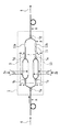
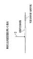
- FIG. 1A shows an example of the configuration of a QPSK modulator
- FIG. 1B shows an intensity waveform and signal point arrangement of optical signals at points A to G in the QPSK modulator of FIG. 1A as an outline of the operation of the QPSK modulator.
- the QPSK modulator 1 includes a Mach-Zehnder Interferometer (MZI), which is called a parent MZI, and an MZI modulator (child MZI modulator) nested in each arm waveguide portion.
- MZI Mach-Zehnder Interferometer
- child MZI modulator child MZI modulator
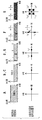
- FIG. 2 shows in detail the operation of the child MZI or single MZI modulator.
- the modulator is assumed to be an LN modulator using a lithium niobate (LiNbO 3 : LN) Z-cut substrate, but basically an X-cut substrate is also used. The operation is similar.
- the drive data electric signal Vdrv 2 is separated into two outputs by the differential output drive circuit 3, and the modulation optical phase shifter of the upper arm of the modulator is used.
- the drive electrode 4 and the lower arm modulation optical phase shifter 5 are differentially input (+ V drv / 2 to the lower arm and ⁇ V drv / 2 to the lower arm) to perform so-called push-pull driving.
- the drive electrode is usually disposed between the modulator arms, and a reverse electric field is applied to the upper and lower arms, so that push-pull driving is automatically performed.
- the continuous (Continuous Wave, CW) light 6 input to the single MZI modulator is bifurcated by the 3 dB optical coupler 7a and then subjected to phase modulation by the upper and lower arm modulation optical phase shifters 4 and 5, respectively.
- the signals are merged again at the 3 dB optical coupler 7f.
- FIG. 2B The state of the phase modulation at this time is shown in FIG. 2B.
- the arrow shown in FIG. 2B is the electric field vector of the output signal light 8. Since the light passing through the upper arm is subjected to phase modulation in the plus direction, the electric field vector draws a locus in a counterclockwise direction (X ⁇ white circle ⁇ black circle), and the light passing through the lower arm is subjected to phase modulation in the minus direction. The electric field vector draws a clockwise trajectory. Since the vector combination of both electric fields becomes the electric field vector of the output signal light, the locus of the output signal light draws a straight locus on the real axis.
- FIG. 2B The arrow shown in FIG. 2B is the electric field vector of the output signal light 8. Since the light passing through the upper arm is subjected to phase modulation in the plus direction, the electric field vector draws a locus in a counterclockwise direction (X ⁇ white circle ⁇ black circle), and the light passing through the lower arm is subjected to phase modul
- the single MZI modulator when the single MZI modulator is driven by a data electrical signal so as to change the phase difference between the arm waveguides by 2 ⁇ , the output light is phase-modulated to phase 0 and ⁇ and signal timing is obtained. Sometimes, the signal light intensity is modulated to a phase binary value having a constant value.
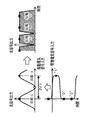
- the single MZI modulator operates as an optical phase modulator. The optical phase modulation by this single MZI modulator is compared with the optical phase modulation by an optical phase modulator composed only of a simple optical phase shifter, as shown in FIG.
- FIG. 2C due to the non-linear behavior of MZI, Produces a phase-shift keying (PSK) signal because it has the advantage that the optical signal output hardly fluctuates even if the drive amplitude of the electrical signal fluctuates somewhat, and also has the feature that the spread of the modulation spectrum is narrow. It is preferably used as a modulator.
- FIG. 2D is a simplified representation of the single MZI modulator 13.
- the CW light branched by the 3 dB coupler 7c is modulated in phase binary by the child MZI modulators (Ich MZI modulator 9 and Qch MZI modulator 10). 1D) and 90 ° phase shift by the ⁇ / 2 optical phase shifter 11 (see F in FIG. 1B), and the 3 dB coupler 7d synthesizes these modulation signals.
- G of 1B QPSK signal light modulated into a phase 4 value is obtained.
- the ⁇ / 2 optical phase shifter is actually realized by adjustment by the subsequent phase adjuster (variable optical phase shifter) 12, and is omitted without being provided separately as a ⁇ / 2 optical phase shifter. There are many.
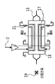
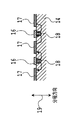
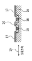
- FIG. 3 shows a detailed configuration in the case where the single MZI modulator is manufactured with an optical waveguide (LN waveguide) formed by titanium diffusion on an LN substrate.
- FIGS. 3A and 3B show the configuration when a Z-cut substrate is used
- FIGS. 3C and 3D show the configuration when an X-cut substrate is used.
- FIG. 3B is a cross-sectional view taken along IIIB in FIG. 3A, and FIG.
- a high-frequency center electrode 16 is provided above the waveguide 15, and a GND electrode 17 is provided around the high-frequency center electrode 16.
- the high-frequency center electrode 16 has a traveling wave electrode structure in which one end is used as a signal input terminal and a termination resistor 21 is connected to the other end in accordance with the propagation direction of light in the waveguide. Modulation is possible. Although not shown in the figure, an electrode having a lumped constant electrode structure may be provided for adjusting the operating point separately from the high frequency electrode. Further, in the subsequent drawings, the single MZI modulator is simply expressed as shown in FIG. 2D as needed regardless of the Z-cut substrate and the X-cut substrate.
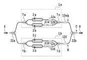
- FIG. 4A shows a configuration of a 16QAM modulator
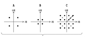
- FIG. 4B shows a signal point arrangement of optical signals at points A to C in the modulator of FIG. 4A.
- the 16QAM modulator includes one 1-input 2-output 2: 1 optical coupler 22a, two QPSK modulators 1a and 1b, two optical phase adjusters (variable optical phase shifters) 12e and 12f, and one It consists of a 2: 1 coupler 22b with 2 inputs and 1 output.
- the input CW light 6 is branched by the 2: 1 optical coupler 22a, individually QPSK modulated by the respective QPSK modulators 1a and 1b, and joined by the 2: 1 optical coupler 22b. Since the ratio of the electric field amplitude of the QPSK signal 1 via the QPSK modulator 1a and the QPSK signal 2 via the QPSK 1b is 2: 1, the relative phase between the QPSK signal 1 and the QPSK signal 2 is appropriately adjusted by the phase adjusters 12e and 12f. Thus, a 16QAM signal can be generated as shown in FIG. 4B. (Non-Patent Document 1)
- FIG. 5A shows a configuration of a conventional two-subcarrier multiple QPSK modulator
- FIG. 5B shows a signal spectrum and signal point arrangement at points A to F in the modulator of FIG. 5A.
- the two-subcarrier multiplexed QPSK modulator includes a 1-input 2-output interleaved optical filter (ILF) 23, two QPSK modulators 1a and 1b, and two optical phase adjusters (variable optical phase shifters) 12e and 12f. It consists of a 2-input, 1-output 3 dB optical coupler 7g.
- IPF 1-input 2-output interleaved optical filter
- Transmission characteristic T B, the transmission characteristic T C of C side to the B side is expressed by the following equation.
- CW light having two wavelengths separated by ⁇ f is input as a subcarrier to this modulator.
- the input two-wavelength subcarriers are demultiplexed by the ILF 23, individually QPSK modulated by the respective QPSK modulators 1a and 1b, and merged by the 3 dB optical coupler 7g. In this way, a subcarrier multiplexed signal can be generated (Non-Patent Document 2).
- a multi-level modulation signal having a large multi-level number such as a 16QAM modulation signal can increase the amount of information that can be transmitted in one symbol without increasing the frequency occupied bandwidth, but the interval between signal points in the signal space is narrow. Therefore, there is a problem that the tolerance to noise, that is, the tolerance to signal-to-noise intensity ratio (SNR) degradation is deteriorated.
- SNR signal-to-noise intensity ratio
- the SNR degradation resistance does not decrease so much, but the frequency occupation band becomes large because multiplexing is performed on the frequency axis. there were.
- the SNR in order to secure a certain communication capacity, it is necessary to at least either keep the SNR high or widen the occupied bandwidth. Since the SNR deteriorates due to spontaneous emission light noise generated in an optical amplifier provided in the transmission line, the SNR becomes lower as the transmission line has a longer transmission distance and a larger number of passes through the optical amplifier. Therefore, from the viewpoint of efficient operation of the transmission path, it is desirable to use these modulation methods properly according to the SNR of the transmission path determined by the transmission distance and the like. That is, it is desirable to use a signal format with a small occupied bandwidth even if the SNR degradation tolerance is not so good as in the 16QAM modulation method in a transmission section where the transmission distance is short and a high SNR can be secured.
- the conventional modulator has a configuration dedicated to each modulation format, and there is a problem that a modulator must be prepared for each format when performing the above-described efficient operation.
- the modulator when performing flexible network operation such as dynamically switching the transmission section according to the traffic state of the network, the modulator must be replaced with a change in the distance of the transmission section. There was a problem that could not be handled.
- the present invention has been made in view of such problems, and an object thereof is to provide an optical modulator that supports a plurality of modulation formats with the same modulator.
- the modulator of the present invention includes a distribution unit 28, an optical modulator array 29 that individually modulates output light from the distribution unit 28, and an aggregation unit 30 that combines output light from the modulator array 29.
- the distribution unit includes an optical demultiplexing / optical branching switchable circuit 31 that can be used by switching between an optical demultiplexing function and an optical branching function.
- the aggregation unit includes a variable merging circuit capable of merging signal lights at an arbitrary ratio and / or an optical merging / light merging switchable circuit 32 that can be used by switching between the light merging function and the light merging function.
- This modulator can demultiplex the carrier light by outputting the optical demultiplexing function according to the number of carrier lights to be modulated, and outputs the signal light modulated for each individual wavelength. Therefore, a carrier multiplexed signal can be generated.
- the distribution unit exhibits a variable branch function according to the modulation multi-level number, and multi-level modulation by electric field synthesis by adjusting the power distribution ratio to each optical modulator in conjunction with the variable merge function of the aggregation unit A signal can be generated. In this way, by changing the operations of the distribution unit and the aggregation unit, it is possible to switch and generate a plurality of modulation formats having different numbers of carriers and modulation multi-values.
- the distribution unit includes a variable 1 ⁇ M branching / branching device configured by connecting one or more variable ILFs in multiple stages, and / or a 1 ⁇ M variable FFT interferometer, and / Or a structure comprising an ILF, a variable optical coupler, and an optical switch, wherein the ILF and the variable optical coupler are switched by the optical switch, and / or the variable optical coupler is connected in a tree shape, and either one of the outputs of each variable optical coupler 2 ⁇ 1 optical switch is inserted.
- the optical modulator array includes a plurality of optical modulators.
- the aggregating unit has a structure composed of one or a plurality of variable optical couplers connected in an inverse tree shape, and / or a structure composed of a plurality of variable attenuators connected in an inverse tree shape, and / or connected in an inverse tree shape.
- the distribution unit can switch between the optical demultiplexing function and the variable optical branching function, and the aggregation unit combines the signal light from the modulator at an arbitrary ratio, and / or is variable with the optical multiplexing function.
- the optical merge function can be switched.
- the optical modulator of the present invention can use a plurality of optical modulators as modulators for each carrier or as an electric field synthesis type multi-level modulator, and the ratio between the number of carriers to be modulated and the number of modulated multi-levels can be freely set. Can be changed. Therefore, it is possible to support a plurality of modulation formats, in particular, a plurality of modulation formats having different occupied bandwidths and SNR degradation tolerances, and to dynamically switch these modulation formats with a modulator having the same configuration.
- the conventional single MZI modulator is a configuration diagram of a case of manufacturing using Z-cut substrate of LiNbO 3.
- FIG. 3B is a cross-sectional view of the single MZI modulator in FIG. 3A at IIIB.
- the conventional single MZI modulator is a configuration diagram of a case of manufacturing using X-cut substrate of LiNbO 3.
- FIG. 3D is a cross-sectional view of the single MZI modulator of FIG. 3C at IIID. It is a figure which shows the structure of the conventional 16QAM modulator.
- FIG. 4B is a signal point arrangement diagram of an optical signal at each of points A to C of the waveguide of FIG. 4A. It is a figure which shows the structure of the conventional 2 subcarrier multiplexing QPSK modulator.
- FIG. 5B is a spectrum of optical signals at each of points A to F of the waveguide of FIG.
- FIG. 13A, FIG. 13B, and FIG. 13C shows the relationship of FIG. 13A, FIG. 13B, and FIG. 13C.
- 13A, 13B, and 13C are one table.
- 13A, 13B, and 13C are one table.
- 15A and FIG. 15B are one table.
- FIG. 15A and FIG. 15B are one table. It is a detailed block diagram of the distribution part concerning the 1st Embodiment of this invention. It is a figure which shows the calculation transmission characteristic of TILF1-1 single-piece
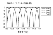
- FIG. 19 is a diagram showing calculated transmission characteristics of TILFs 2-1 and 2-2 alone when the configuration parameters of FIG. 18 are used. It is a figure which shows the calculation transmission characteristic of the whole distribution part at the time of using the structure parameter of FIG.
- FIG. 20 20
- ILF interleave filter
- VC variable optical coupler
- the optical switch which switches these.
- TILF of the distribution part concerning the 1st Embodiment of this invention is a block diagram of the high-extinction ratio version of the variable coupler built-in type TILF based on single MZI. It is a structural example of TILF of the distribution part concerning the 1st Embodiment of this invention, and is a block diagram of TILF with a built-in variable coupler based on a lattice type interferometer. It is a structural example of TILF of the distribution part concerning the 1st Embodiment of this invention, and is a block diagram of the high-quenching specific version of the variable coupler built-in type TILF based on the lattice type interferometer.
- FIG. 1 It is a block diagram at the time of comprising the distribution part concerning the 1st Embodiment of this invention with the variable interferometer type FFT interferometer. It is the figure which comprised the aggregation part concerning the 1st Embodiment of this invention with the variable optical coupler. It is the figure which comprised the consolidating part concerning the 1st Embodiment of this invention by the combination of a variable attenuator and a 2 * 1 optical coupler. It is the figure which comprised the consolidating part concerning the 1st Embodiment of this invention by the combination of a variable coupler type and a variable attenuator type.
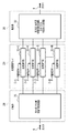
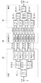
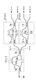
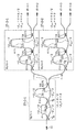
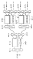
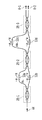
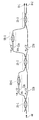
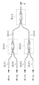
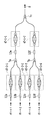
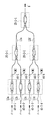
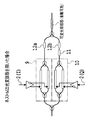
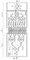
- FIG. 7 shows the configuration of a format variable optical modulator according to the first embodiment of the present invention.
- the modulator configuration of this embodiment includes a variable 1 ⁇ M I / F demultiplexing filter 24 configured by connecting variable 1 ⁇ 2 ILFs in multiple stages, M phase modulators (PSK modulators) 13-1 to 13-4, and M / 2 2 input 1 output optical couplers 7g, 7h and (M / 2) input 1 output variable optical coupler 25.
- Variable ILFs (Tunable ILF) 27-1-1 to 27-2-2 are optical path length differences ⁇ L sandwiched between two 3 dB optical couplers 7a to 7f; where the optical path length difference is not a waveguide length difference Is a value converted into a length in vacuum in consideration of the refractive index of the waveguide; and includes a delay line and variable optical phase shifters 12a to 12f, and has a free spectral range (FSR) according to a known interference principle.
- FSR free spectral range
- the absolute position of this period on the frequency axis can be shifted by adjusting the relative phase of the two optical paths using the variable phase shifters 12a to 12f.
- the variable optical coupler (VC) 25 includes variable optical phase shifters 12g and 12h sandwiched between two 3dB optical couplers 7i and 7j. The relative phase of the two optical paths is adjusted using the variable phase shifters 12g and 12h. By adjusting, the merging ratio can be set to a desired value.
- the transmission characteristic of the variable optical coupler 25 is expressed by the following equation based on a known interference principle.
- T 1 is a transmission characteristic of light transmitted from the variable optical phase shifter 12-1-1 side to the output port
- T 2 is a transmission characteristic of light transmitted from the variable optical phase shifter 12-1-2 side to the output port. It is a characteristic.
- ⁇ is the phase difference of the interference arm sandwiched between the two 3 dB optical couplers; the phase difference of the light on the upper arm side with respect to the light on the lower arm side; controlled by the variable phase shifters 12g and 12h Is done.
- the VC having such a configuration is called an interferometer-type variable optical coupler.
- an interferometer-type variable optical coupler for example, a configuration in which the coupling ratio of the directional coupler is changed or a configuration in which the waveguide structure of the Y branch is changed, Of course.
- the 1-input 2-output or 2-input 1-output optical coupler, variable optical coupler (VC), and variable ILF (TILF) use a 2-input 2-output configuration, and an unnecessary input / output port is used as the main signal path. It is good also as a structure which is not connected. Further, the ⁇ / 2 optical phase shifters 11-1 and 11-2 arranged at the subsequent stage of the PSK modulators 13-2 and 13-4 are arranged at the rear end of the ⁇ / 2 optical phase shifter. Since it can be realized by adjustment using the variable optical phase shifters 12-2-1 to 12-2-4, it may be omitted.
- variable optical phase shifters 12a to 12f that are paired in each TILF adjust the relative phase in the TILF, and therefore one of the variable optical phase shifters 12a to 12f that are paired. It is also possible to provide only the configuration.
- the variable optical phase shifters 12-2-1 and 12-2-2 which are paired with the PSK modulators 13-1 and 13-2, output light from the PSK modulators 13-1 and 13-2. Since the relative phase is adjusted, a configuration in which only one of the variable optical phase shifters 12-2-1 and 12-2-2 is provided may be used.
- the variable optical phase shifters 12-2-3 and 12-2-4 of the PSK modulators 13-3 and 13-4, and the variable optical phase shifters 12-1-1 and 12- arranged at the front stage of the VC25.
- variable phase shifters 12-2-1 to 12-2-4, 12-1-1 and 12-1-2 are used when the relative phase of the output light from the PSK modulator deviates from a desired value. Since the deviation is corrected, it can be omitted if there is no deviation due to the improvement of the production accuracy or the application of the trimming technique. These omissions and replacements are the same in the following embodiments and examples unless otherwise specified.
- the optical path length difference between the delay lines of TILF27-1-1 to 27-2-2 is that the FSR of TILF27-1-1 is twice the carrier interval ⁇ f, and the FSR of TILF27-2-1 and 27-2-2 is It is designed to be four times the carrier interval ⁇ f.
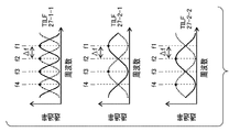
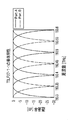
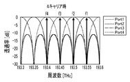
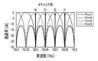
- this modulator is operated as a four-carrier BPSK modulator, the variable optical phase shifters 12a to 12f are adjusted so that the transmission characteristics of TILF become the characteristics shown in FIG. 8A.
- the TILF 27-1-1 adjusts so that the carrier lights of the frequencies f1 and f3 are demultiplexed to the port on the TILF 27-2-1 side, and the carrier lights of the frequencies f2 and f4 are demultiplexed to the port on the TILF 27-2-2 side.
- the TILF 27-2-1 adjusts so that the carrier light of f1 is demultiplexed to the port on the PSK modulator 13-1 side and the carrier light of f3 is demultiplexed to the port on the PSK modulator 13-2 side.
- the TILF 27-2-2 adjusts so that the carrier light of f2 is demultiplexed to the port on the PSK modulator 13-3 side and the carrier light of f4 is demultiplexed to the port on the PSK modulator 13-4 side.
- the VC 25 adjusts the variable phase shifters 12g and 12h so that the coupling rate is 3 dB.
- the four input carrier lights are demultiplexed by these TILFs, and then four PSKs are input.
- BPSK modulation is performed by the modulator, and the signals are equally combined by the 3 dB couplers 7g and 7h and the VC 25, and a 4-carrier BPSK modulated signal is output.
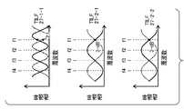
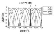
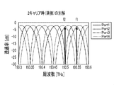
- variable optical phase shifters 12a to 12f are adjusted so that the transmission characteristics of TILF become the characteristics shown in FIG. 8B. That is, the TILF 27-1-1 adjusts so that the carrier light of f1 is demultiplexed to the port on the TILF 27-2-1 side and the carrier light of f2 is demultiplexed to the port on the TILF 27-2-2 side. 27-2-2 are adjusted to operate as 3 dB couplers at carrier frequencies f1 and f2, respectively.
- the relative phase difference of the optical signals output from the PSK modulators 13-1 and 13-2 is appropriately adjusted using the variable optical phase shifters 12-2-1 and 12-2-2 so that the relative phase difference becomes ⁇ / 2. Keep it.
- the output optical signals from the PSK modulators 13-3 and 13-4 are also adjusted as appropriate using the variable optical phase shifters 12-2-3 and 12-2-4.
- the TILF 27-2-1, the PSK modulators 13-1, 13-2, and the 3 dB optical coupler 7g are operated as one QPSK modulator A as a whole
- the TILF 27- The 2-2, PSK modulators 13-3 and 13-4, and the 3 dB optical coupler 7h are also operated as another QPSK modulator B as a whole.
- the VC 25 adjusts the variable phase shifters 12g and 12h so that the coupling rate is 3 dB.
- the present modulator is equivalent to a configuration in which the QPSK modulators A and B are connected in parallel between the TILF 27-1-1 and the VC 25 which is a 3 dB coupler.
- the two input carrier lights are demultiplexed by TILF27-1-1.
- QPSK modulation is performed by these two QPSK modulators A and B, respectively, and then VC25 is equally joined to output a 2-carrier QPSK modulated signal.
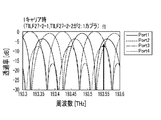
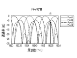
- variable optical phase shifters 12a to 12f are adjusted so that the transmission characteristics of TILF are the characteristics shown in FIG. 8C. That is, the TILF 27-1-1 is adjusted to operate as a 2: 1 coupler at the carrier frequency f1, and the TILFs 27-2-1 and 27-2-2 are also adjusted to operate as a 3 dB coupler at the carrier frequency f1.
- the VC 25 adjusts the variable phase shifters 12g and 12h so that the coupling ratio is 2: 1. It should be noted that the relative phase difference of the optical signals output from the PSK modulators 13-1 and 13-2 is appropriately adjusted using the variable optical phase shifters 12-2-1 and 12-2-2 so that the relative phase difference becomes ⁇ / 2. Keep it.
- the output optical signals from the PSK modulators 13-3 and 13-4 are also adjusted as appropriate using the variable optical phase shifters 12-2-3 and 12-2-4.
- the TILF 27-2-1, the PSK modulators 13-1, 13-2, and the 3 dB optical coupler 7g operate as a single QPSK modulator A as a whole
- the TILF 27- The 2-2, PSK modulators 13-3 and 13-4, and the 3 dB optical coupler 7h also operate as another QPSK modulator B as a whole.
- the entire TILF 27-1-1 and VC25 operate as a 16QAM modulator.
- variable optical phase shifters 12-1-1 and 12-1-2 are appropriately adjusted so as to be the same as the IQ axis on the signal point arrangement diagram of the output optical signal of the QPSK modulator B.
- the input carrier light is branched 2: 1 by TILF27-1-1, and then QPSK modulator A and QPSK modulator B is individually QPSK modulated and merged with a 2: 1 coupler. Since the 2: 1 branching ratio / merging ratio is a ratio in electric power, the branching ratio / merging ratio in electric field amplitude is the square ratio, that is, ⁇ 2: 1.
- the ratio of the electric field amplitude of the QPSK signal A via the QPSK modulator A and the QPSK signal B via the QPSK modulator B is 2: 1 because it is the product of the ratio at the branch and the ratio at the merge.
- a 1-carrier 16QAM modulated signal as described in C of FIG. 4B is output.
- both the branching ratio in TILF27-1-1 and VC25 have a coupling ratio of 2: 1, but other combinations, for example, the branching ratio in TILF27-1-1 is 4: 1, and VC25 is coupled.
- the electric field amplitude ratio of the signal via QPSK modulators A and B is 2: 1, so that a 1-carrier 16QAM modulated signal can be output.
- the ratio of branching and merging is made different in this way, a principle loss generally occurs, which is not preferable, and it is preferable to set the same ratio as in this embodiment. It should be noted that this is true not only in the synthesis of 16QAM signals but also in the synthesis of QPSK signals in QPSK modulators A and B.
- the modulator of the configuration of the present invention only needs to adjust TILF and VC, such as a 4-carrier BPSK signal, a 2-carrier QPSK signal, a 1-carrier 16QAM signal, and the like.
- the modulation format can be switched. Since a BPSK signal can send 1-bit information per symbol, a 4-carrier BPSK signal can send 4-bit information per symbol. Since a QPSK signal can send 2 bits of information in 1 symbol, a 2 carrier QPSK signal can also send 4 bits of information in 1 symbol, and a 16 QAM signal can send 4 bits of information in 1 symbol, so 1 carrier 16QAM signal is also 1 4-bit information can be sent in symbols.
- the three types of modulation signals all achieve the same transmission rate.
- the 4-carrier BPSK signal occupies a band corresponding to 4 carriers, it has excellent SNR degradation tolerance, whereas the 1-carrier 16QAM signal, on the contrary, does not have excellent SNR degradation tolerance, but occupies only 1 carrier.
- the 2-carrier QPSK signal is intermediate. Therefore, the present modulator can switch and generate an optimum modulation format signal with the same configuration from among a plurality of modulation formats having different occupied bandwidths and different SNR degradation tolerances, and can also generate a variable phase shift. It can be switched at high speed only by adjustment with the instrument.
- the optical phase shifter portion is used as described later in microseconds or less. Even when a quartz-based waveguide is used, a switching speed of about milliseconds can be realized.
- the data signal which is the main signal is not changed at all.
- the driving circuit, the band of the modulator, and the like require high performance in accordance with the maximum rate.
- an electric filter is additionally required in order to prevent unnecessary spectral spread in the output signal, when operating at a low symbol rate, and an electric filter is additionally required. It becomes complicated. Since this modulator can be switched without making any such changes to the data signal, the configuration of the peripheral circuit can be kept simple, and the bandwidth of the modulator has a constant symbol rate.
- the device can be designed only for the device. Accordingly, an optical modulator that supports a plurality of modulation formats can be provided at low cost.
- the modulator of the present invention can easily change the modulation signal format in order to perform efficient transmission according to the SNR determined in the transmission section, that is, the distance, and can be switched at high speed. Therefore, the optimum format can be dynamically selected even in the case of performing flexible network operation such as dynamically switching the transmission section according to the traffic state of the network.
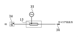
- FIG. 9 is an example of a multicarrier light source.
- FIG. 9A shows a method of generating multicarriers by modulating the seed light source 34 (wavelength f0) using the single MZI modulator 13.
- FIG. In the case of one carrier, the seed light source itself is set as the carrier light source f1 ( f0) by applying a bias for simply performing the Open operation without performing modulation.
- the number of carriers generated can be increased by increasing the drive amplitude.
- carriers cannot be generated with the same intensity of all the generated carriers. Therefore, when the number of carriers exceeds 4, some level adjustment mechanism is required.
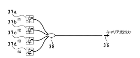
- FIG. 9B shows a simple configuration in which the wavelength variable light sources 37a to 37d are simply arranged and the outputs are combined by the optical coupler 38.
- the number of carriers to be output is changed by causing the light source to emit light according to the required number of carriers.
- This configuration is disadvantageous in that light sources corresponding to the maximum number of carriers are required, but it is advantageous in that it can cope with a case where the carrier intervals are unequal.
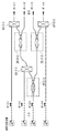
- the modulator of the present invention is roughly divided into a distribution unit 28, an optical modulator array 29, and an aggregation unit 30.
- the distribution unit has a configuration in which TILFs 27-1-1 to 27-2-2 are connected in a tree shape in multiple stages, and the optical modulator array is an MZI type array arranged in an array shape.
- the PSK modulators (PSK) 13-1 to 13-4 are configured, and the aggregation unit is configured such that VCs 25-1-1 to 25-2-2 are connected in multiple stages in an inverted tree shape.
- the VCs 25-1-1 and 25-1-2 in the first stage are the normal 3 dB optical couplers 7g and 7h, respectively.
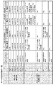
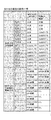
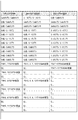
- the signal of three types of modulation formats can be switched and generated as shown in the table of FIG. 11 by combining the operation of each element of the distribution unit and the aggregation unit of this modulator.
- the names TILF1-1 to 2-2, VC1-1 to 2-2, and PSK1 to PSK1 to 4 are indicated by the names shown in FIG.
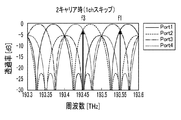
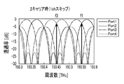
- the carrier signal when generating a 2-carrier QPSK signal, the case where a carrier signal uses an adjacent channel (ch) has been described. However, in this modulator, the carrier signal skips 1ch other than that. It is also possible to generate a 2-carrier QPSK signal with respect to the carrier signal having a 2ch interval.
- the TILF 27-1-1 is set to operate as a 3 dB coupler, and the TILFs 27-2-1 and 27-2-2 are set to operate as a duplexer, PSK 13-1 and PSK 13-3 generate a QPSK signal of frequency f1, and PSK 13-2 and PSK 13-4 generate a QPSK signal of frequency f3.
- the operation 1 is the operation described above, but there is an operation 2 in addition to this.
- the TILF 27-1-1 and VC24-1-1 are operated as 3 dB couplers for the frequency f1, and the TILFs 27-2-1 and 27-2-2, VC24-2-1 and 24-2-2 are operated.
- PSK 13-1 and 13-3 By operating as a 2: 1 coupler, PSK 13-1 and 13-3 generate a QPSK signal with an electric field amplitude of 2, and PSK 13-2 and 13-4 generate a QPSK signal with an electric field amplitude of 1.
- a 16QAM signal is generated.
- the table of FIG. 11 shows only the case where all the PSK modulators are driven, it is of course possible to use only a part of the PSK modulators.
- the operation of the modulator is in a state in which a 4-carrier BPSK signal is generated.
- the input carrier light is only f1
- the PSK modulator to be driven is only PSK13-1, so that the 1-carrier BPSK signal is generated.
- the modulator is set in a state of generating a 2-carrier QPSK signal for adjacent channel operation, the input carrier light is only f1, and the PSK modulator to be driven is only PSK13-1 and PSK13-2. By doing so, it is possible to generate a one-carrier QPSK signal.
- the transmission rate decreases as the number of carriers is reduced. Also in the following embodiments, although not specifically illustrated, it is previously noted that a modified operation mode in which the number of carriers is reduced is also included.
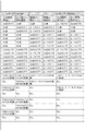
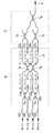
- FIG. 12 a list of operation states for generating various signal formats is shown in the tables of FIGS. 13A, 13B and 13C.
- the names TILF1-1 to 3-4, VC1-1 to 3-4, and PSK1 to 8 of the respective codes are described with the names shown in FIG.
- FIGS. 13A, B, and C One table is shown in FIGS. 13A, B, and C.
- four types of signals that is, an 8-carrier BPSK signal, a 4-carrier QPSK signal, a 2-carrier 16 QAM signal, and a 1-carrier 256 QAM signal can be switched and generated. Even in this configuration, if the operation mode is limited, a part of VC can be replaced with a normal 3 dB fixed coupler.
- the number of light modulation arrays is reduced from 16 to 12.
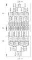
- Examples of operating states for generating specific various signal formats are shown in the tables of FIGS. 15A and 15B.
- One table is shown in FIGS. 15A and 15B.
- the names TILF / VC 1-1 to 4-4 and PSK1 to 12 of the respective codes are indicated by the names shown in FIG.
- this modulator it is possible to switch and generate five types of signals: a 12-carrier BPSK signal, a 6-carrier QPSK signal, a 3-carrier 16 QAM signal, a 2-carrier 64 QAM signal, and a 1-carrier 4096 QAM signal.
- one carrier 4096 QAM signal is omitted.
- M 4 as the distribution unit form 1.
- Each of the TILFs 27-1-1 to 27-2-2 has an MZI configuration in which two 2-input 2-output 3 dB optical couplers 7a to 7f are sandwiched by delay lines with variable optical phase shifters 12a to 12f. Yes.
- the optical path length difference between the delay lines of TILF 27-1-1 is 2 ⁇ L
- the optical path length difference between TILFs 27-2-1 and 27-2-2 is ⁇ L.
- ⁇ L c / (M ⁇ ⁇ f).
- the optical couplers 7a to 7f are all configured with two inputs and two outputs, and one input of the input side optical coupler is not connected.
- the input side optical coupler may be configured with one input and two outputs.
- any method such as a directional coupler, a multi-mode waveguide configuration, or a kind of interferometer called a wavelength-independent coupler (WINC) may be used.
- a Y branch may be used. The same applies to the forms described below.
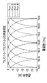
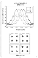
- FIG. 16B shows the calculated transmission characteristics of the TILF 27-1-1 alone when an ideal directional coupler is used.
- FIG. 16C shows calculated transmission characteristics of TILFs 27-2-1 and 27-2-2 alone.
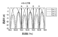
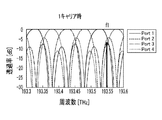
- FIG. 17 shows the calculation characteristics of the entire distribution unit.
- the arrow line in the figure schematically shows the frequency position of the carrier signal used in each mode. As shown here, it can be seen that each carrier is branched by a demultiplexing or an appropriate branching ratio in each operation state.
- the characteristics of the distribution unit have a periodic characteristic. Therefore, the carriers need not necessarily be arranged adjacent to each other, and may be arranged at periodically separated frequencies. For example, in FIG. 17A, the carrier of f2 is arranged at 193.5 THz, but it may be arranged at 193.7 THz, 193.3 THz, etc. separated by a period of 200 GHz in this design.
- FIG. 18 shows an example in which the TILF of the distribution unit is configured by a lattice type interferometer as the distribution unit configuration 2.
- the lattice type interferometer has a structure in which MZIs are connected in a multi-stage lattice shape, and the phase state of the MZI in each stage and the coupling rate of the coupler are determined. Since it can be set individually, there is an advantage that the degree of freedom in designing the transmission characteristics increases as the number of lattice stages increases. On the other hand, the disadvantage is that the circuit length becomes longer depending on the number of stages of the lattice.
- the optical path length difference of TILF27-1-1 is ⁇ L at the first stage close to the input side and 2 ⁇ L at the second stage close to the output side
- TILF27-2-1, 27 The optical path length difference of -2-2 is 2 ⁇ L in the first stage and 4 ⁇ L in the second stage.
- the basic unit ⁇ L of the optical path length difference is the same as in the case of simple MZI.
- connection order of the TILF is the order in which the FSR is small, that is, the order in which ⁇ L is large.
- the arrangement of the extinction ch and the transmission ch can be changed, so that the arrangement of the TILF connection can be switched.
- the FSR of the TILF 27-1-1 is 4 ⁇ f
- the FSR of the TILFs 27-2-1 and 27-2-2 is 2 ⁇ f
- the TILF having a large FSR is arranged in the first stage.
- FIG. 19C, D, and E show the calculated transmission characteristics of the entire distribution unit.
- TILF27-1-1 may be mixed as a lattice type
- TILF27-2-1 and 27-2-2 may be combined as a simple MZI type. good.
- FIG. 20 shows an example in which the distributing unit is configured with an M-demultiplexed FFT interferometer described in Non-Patent Document 6 as the distributing unit form 3.
- the FFT type interferometer is knitted into a 1-input M-branch coupler 39 with M delay line arrays 40 each having a delay difference of ⁇ L, 2-input 2-output couplers 7d to 7g, and variable optical phase shifters 12a to 12h. It consists of a multi-stage variable M ⁇ M coupler 41 that is connected.
- the 1-input M-branch coupler 39 is configured by connecting the 1-input 2-output optical couplers 7a to 7c in multiple stages, but may be configured using a 1-input M-output MMI coupler or the like. Note that the basic unit ⁇ L of the optical path length difference of the delay line portion is the same as in the case of the simple MZI.
- the k-th stage j-th optical coupler (k is an integer from 1 to n, j is a natural number from 1 to 2 n ⁇ 1 ) couples the Xth path and the Yth path.
- it represents (j-1) div2 n- k and (j-1) mod2 n- k , respectively, and the quotient obtained by dividing (j-1) with 2 n-k, the remainder.
- an optical phase adjuster for adjusting the relative phase of each path is disposed between the stages.
- This configuration has the advantage of being smaller than the configuration in which the simple MZI type or lattice type TILFs are connected in multiple stages because only one delay line is required.
- M increases, the advantage increases.
- the number of variable optical phase shifters is increased compared to a configuration in which TILFs are connected in multiple stages, and there are drawbacks in that control is somewhat complicated and power consumption is increased.
- this configuration the same characteristics can be obtained with the drive patterns of a plurality of variable optical phase shifters.
- ⁇ Distributing part form 4 element switching type>
- the distribution unit is configured such that an interleave filter (ILF) and a variable optical coupler (VC) can be selected by an optical switch at each location.
- the variable operation of the distribution unit is realized by simply switching and using each ILF and VC following the operation in the table of FIG.
- the advantage is that fine adjustment of interference conditions is not required as in the interferometer type filters of the distribution unit forms 1 to 3, but an optical switch is required, so that the overall configuration is complicated.
- the optical switch may have an on / off switching type configuration, or use the same configuration as the variable optical coupler and use operating points of 100% transmission and 0% transmission without using an intermediate region. May be.
- variable optical couplers VCs
- VCs variable optical couplers
- the four carrier light sources emit light at their respective wavelengths, and all the optical switches are switched so as to select the input port side of the distribution unit, that is, each carrier light source side.
- VCs 25-1-1 and 25-2-2 are also used as path selection switches and set so that light from the input port 3 is guided to the output port 3.
- VC25-2-1 is also used as a route selection switch, and is set so that light from input port 2 is guided to output port 2.
- the carrier light sources of the input ports 2 and 3 are made to emit light, and only the optical switch 43-1-1 is set so as to select the input port side of the distribution unit, and the optical switches 43-2-1 and 43-2 are selected.
- -2 is set to select the VC side.
- the VC 25-1-1 is used as a path selection switch, and is set so that light from the input port 3 is guided to the VC 25-2-2.
- the VCs 25-2-1 and 25-2-2 are set to operate as a 3 dB coupler. In the case of one carrier, only the input port 3 emits the carrier light source, and all the optical switches are set to select the VC side.
- VC25-1-1 is set to operate as a 2: 1 coupler, and VC25-2-1 and 25-2-2 are set to operate as a 3 dB coupler. By operating in this way, each modulation format can be switched.
- the on / off switching type configuration may be used for the optical switch in this configuration, or 100% transmission is performed without using the intermediate region by using the same configuration as the 2-input 1-output variable optical coupler. An operating point of 0% transmission may be used.
- This embodiment has an advantage that the wavelength of each carrier light can be arbitrarily set because no duplexer is used.
- a plurality of light sources are necessary, and the plurality of light sources must be connected to a plurality of input ports, respectively, and the configuration including the light sources is a disadvantage.
- ⁇ Distribution part form 6 Simple MZI type with built-in variable coupler> Still another configuration will be described as a distribution unit configuration 6.
- the overall configuration is the same as that of the distribution unit forms 1 and 2, but the configuration of each TILF is different from these.
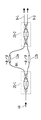
- a configuration of the TILF in this embodiment is shown in FIG. 24A.
- the TILF in this embodiment has an MZI configuration in which a delay line with a variable optical phase shifter is sandwiched between two variable optical couplers.
- each variable coupler has an MZI configuration in which two 3 dB optical couplers are connected via two variable optical phase shifters, but another configuration may be used.
- the optical path length difference of the n-th stage TILF that is, TILF27 ⁇ (n) ⁇ (X) is M ⁇ ⁇ L / 2n .
- the coupling ratio of the variable optical couplers 25-1 and 25-2 is set to 3 dB, and the variable optical coupler is operated as a normal 3 dB coupler.
- the desired optical carrier is demultiplexed into the outputs 8-1 and 8-2 by adjusting in the same manner as in the distribution unit configuration 1 described above.
- this TILF is operated as a branching unit having an arbitrary branching ratio such as a 3 dB optical coupler or a 2: 1 optical coupler
- the variable optical coupler 1 is operated only on either the short arm side or the long arm side of the delay line portion.
- variable optical coupler 25-2 is operated so that the coupling ratio becomes a desired branching ratio, for example, 3 dB or 2: 1.
- the variable optical coupler 25-2 is operated so that the coupling rate is 0% or 100%
- the variable optical coupler 25-1 is operated so that the coupling rate is a desired branching ratio, for example, 3 dB or 2: 1.
- the present TILF can be operated as a branching filter or a branching unit having a desired branching ratio. If the branching ratio during the branching operation is only 3 dB, either the variable optical coupler 1 or the variable optical coupler 2 can be replaced with a fixed 3 dB coupler.
- This form is a form that combines the concepts of the configuration of the distribution part form 1 and the distribution part form 4, and the merits / demerits are located between these two forms.
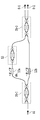
- FIG. 24B shows a configuration in which the characteristics of this embodiment are further improved.
- the variable optical coupler 25-1 or 25-2 when operating as a branching device, the variable optical coupler 25-1 or 25-2 is operated so as to be 0% or 100% coupled.
- a variable optical coupler using such interference is used.
- the configuration of the OnOff switch is an MZI configuration in which two 3 dB optical couplers are connected via two variable optical phase shifters as in the variable optical coupler in this figure, but another configuration may be used.
- the OnOff switch is set in a transparent state.
- this TILF is operated as a branching device having an arbitrary branching ratio
- the variable optical coupler 25-1 is operated so that light is guided to the arm side where the OnOff switch 55 is not provided, and the OnOff switch is turned off.
- the variable optical coupler 25-2 is operated so that the coupling ratio becomes a desired branching ratio, for example, 3 dB or 2: 1.
- the branching operation the operation is performed so that the light is not propagated to the path on the OnOff switch side. However, in this configuration, the propagation light is blocked at two places of the variable optical coupler 25-1 and the OnOff switch.
- the extinction ratio can be doubled as compared with. If the branching ratio during the branching operation is only 3 dB, the variable optical coupler 25-2 can be replaced with a fixed 3 dB coupler.
- ⁇ Distributing part configuration 7 Lattice type with built-in variable coupler> Still another configuration will be described as a distribution unit configuration 7.
- a configuration of the TILF in this embodiment is shown in FIG. 25A.
- the concept of the distribution unit configuration 6 is basically applied to the distribution unit configuration 2, and the configuration of each TILF is not a configuration based on a single MZI, but a configuration based on a lattice type interferometer This is different from the idea in the distribution unit form 6.
- the TILF in this embodiment has a configuration in which variable optical couplers and delay lines with variable optical phase shifters are connected alternately.
- FIG. 25A is a normal type
- FIG. 25B is a high-performance version in which crosstalk from unnecessary paths is reduced during a branching operation.
- variable optical couplers 25-1, 25-2, 25-3 are operated so that the coupling ratios are 3 dB, 3 dB, and 14.6%, respectively, and each OnOff switch 55 -1, 55-2 are set to the transmission state.
- the desired optical carrier is demultiplexed into the outputs 8-1 and 8-2 by adjusting in the same manner as in the distribution unit configuration 2 described above.
- this TILF is operated as a branching device having an arbitrary branching ratio, the variable optical couplers 25-1 and 25-2 are guided to the arm side where the OnOff switches 55-1 and 55-2 are not provided.
- Each OnOff switch is turned off, and the variable optical coupler 25-3 is operated so that the coupling rate becomes a desired branching ratio. If the coupling ratio of the variable optical coupler 25-3 during the demultiplexing operation is 3 dB and the branching ratio during the branching operation is only 3 dB, the variable optical coupler 25-3 can be replaced with a fixed 3 dB coupler. .
- the concept of the distribution unit configuration 6 is applied to the distribution unit configuration 3, and in the FFT interferometer of the distribution unit configuration 3, some or all of the optical couplers are replaced with variable optical couplers.
- an OnOff optical switch is inserted in the delay line portion of the FFT interferometer in order to reduce crosstalk from unnecessary paths during the branching operation. If it is not necessary to improve the crosstalk characteristics, this OnOff optical switch can be omitted.
- the idea of the distribution unit configuration 6 is basically applied to the distribution unit configuration 3, and the advantages and disadvantages are basically the same as those described above.
- each optical carrier is demultiplexed to the ports 1 to 4 by adjusting in the same manner as in the distribution unit configuration 3 described above.
- variable optical couplers 25-1-1, 25-3-2, 25-4-1, 25-4 -2 is operated so that the coupling rate is 3 dB, and the variable optical couplers 25-2-1 and 25-2-2 are operated so that light is guided to the arm side of the delay optical path length difference 2 ⁇ L and 0, respectively.
- the OnOff switches 55-1 and 55-3 are turned off, and the switches 55-2 and 55-4 are turned on.
- the operation state of the variable optical coupler 25-3-1 may be any.
- variable optical couplers 25-2-1 and 25-2-2 are inserted in the middle, but the variable optical coupler 25-1-1, the delay optical path length difference 2 ⁇ L, the interference arm of 0, and the variable light
- the optical carriers f1 and f2 are demultiplexed by appropriately operating the variable optical phase shifter that adjusts ⁇ 2 and ⁇ 4. can do.
- the demultiplexed optical carriers f1 and f2 are branched by 3 dB by the variable optical couplers 25-4-1 and 25-4-2, respectively. Therefore, the same operation as that in the case of two adjacent carriers in the distribution unit configuration 3 is realized.
- variable optical couplers 25-1-1 and 25-2-2 are operated so that light is guided to the arm side with a delay optical path length difference of 0. Then, the variable optical couplers 25-3-2, 25-4-1, and 25-4-2 are operated so that the coupling ratios are 2: 1, 3 dB, and 3 dB, respectively, and the OnOff switches 55-1 to 55-3 are operated. Is cut off, and 55-4 is turned through.
- the operating state of the variable optical couplers 25-2-1 and 25-3-1 may be any. By operating in this manner, the input optical carrier can be branched at a ratio of 2: 2: 1: 1.
- variable optical couplers 25-3-1, 25-4-1 and 25-4-2 always operate at 3 dB, and can be replaced with a fixed 3 dB optical coupler.
- the OnOff switch 55-4 is always in the transmissive state and can be omitted.
- FIG. 27 is a configuration diagram of the variable coupler type aggregating unit which is the aggregating unit form 1.
- This configuration is a generalized configuration of the aggregation unit in the first embodiment.
- a variable optical coupler (VC) is connected in multiple stages in an inverted tree shape, and a variable optical phase shifter is disposed between the input port of the aggregation unit and the variable coupler or between each variable coupler. With such a configuration, light from each input port of the aggregation unit can be combined with the output port at an arbitrary ratio and in an arbitrary relative phase relationship.
- each variable optical phase shifter described above is intended to adjust the relative phase of light from each input port of the aggregating unit, and therefore, the first stage variable optical phase shifters 12-2-1 to 12-2-4. Only the remaining variable optical phase shifters 12-1-1 and 12-1-2 can be omitted. However, it is easier to adjust the relative phase if a variable optical phase shifter is provided at each stage. As another method of omitting each of the variable optical phase shifters described above, the variable optical phase shifters 12-1-1 and 12-1-2 are paired with the light from the VC 25-2-1 and the VC 25-2.
- variable optical phase shifters 12-2-1 and 12-2-2 and the variable optical phase shifters 12-2-3 and 12-2-4 the variable optical phase shifters 12-2-1 to 12-2-4 between the input port of the aggregation unit and the variable coupler can be omitted if a variable phase function is provided on the optical modulator side. is there.
- these variable phase shifters are for correcting the deviation when the relative phase of the output light of the optical modulator array deviates from a desired value. If there is no deviation due to the application of the trimming technique or the like, these variable phase shifters can be omitted.
- Each variable optical coupler has an MZI configuration in which, for example, a 2-input 2-output 3 dB optical coupler and a 2-input 1-output 3 dB optical coupler are connected via two variable optical phase shifters.
- the 2-input 1-output 3 dB optical coupler may be substituted by using a 2-input 2-output 3 dB optical coupler and disconnecting one of the outputs.
- any method such as a directional coupler, a multi-mode waveguide configuration, or a kind of interferometer called a wavelength independent coupler (WINC) may be used.
- variable optical couplers may use not only the MZI configuration but also other configurations such as a configuration in which the coupling ratio as a coupler is changed by changing the refractive index of the coupling portion of the directional coupler. The same applies to the subsequent embodiments.
- FIG. 28 shows the configuration of the aggregation unit form 2.
- the variable coupler unit of the variable coupler type (aggregation unit form 1) is replaced with a combination of a variable attenuator and a 2-input 1-output optical coupler.
- the attenuation amount of the variable attenuator by adjusting the attenuation amount of the variable attenuator, the light from each input port of the aggregation unit can be combined with the output port at an arbitrary ratio and in an arbitrary relative phase relationship.
- a principle loss occurs in the operation other than the merge at the equal ratio.
- Such a principle loss does not occur in the variable coupler type (aggregation unit form 1).
- this configuration has an advantage that it is easy to adjust the level of light from each input port of the aggregation unit because the variable attenuator is individually provided for each input port of the aggregation unit.
- FIG. 29 shows the configuration of the aggregation unit form 3.
- This configuration is a combination of a variable coupler type and a variable attenuator type.
- this figure shows a configuration in which optical monitors 46-1 to 46-4 are provided after the variable attenuators 45-3-1 to 45-3-4.
- optical monitors 46-1 to 46-4 are provided after the variable attenuators 45-3-1 to 45-3-4.
- various adjustments can be performed while grasping the signal state from each port by appropriately providing an optical monitor.
- the optical monitor can be similarly provided in other forms such as forms 1 and 2.
- FIG. 30 shows the configuration of the aggregation unit form 4.
- ⁇ L of the FFT distribution unit is set to 0, and the input and output are switched.
- ⁇ Aggregating unit form 5 with harmonic cut filter>
- the optical signals from the light modulation array unit are basically joined. If the signal of each carrier has a high level harmonic component, that is, if it has a large sidelobe spectrum, this sidelobe may become crosstalk with respect to the adjacent carrier. Normally, this side lobe is not so large, so there is no problem. However, if the frequency characteristics of the optical modulator array are too good and the rectangularity of the drive signal waveform is too good, the side lobe becomes large. become.
- the OBPF is implemented while suppressing the circuit scale by adding some ideas.
- the harmonics of the optical signal become a problem in the first side lobe.
- the intensity of the side lobe rapidly decreases as the second, third and higher order. Therefore, in the case of the modulator of the present invention, OBPF that considers only crosstalk with respect to adjacent carriers is sufficient. Therefore, the OBPF may be a filter that can attenuate adjacent channels, such as ILF. Since the transmission band is repeated every other channel in the ILF, it is only necessary to prepare one ILF for each of the even channel and the odd channel, and it is not necessary to prepare the ILF for each carrier.
- the configuration of FIG. 31 is based on the configuration of the aggregating unit form 1, and a 1-input 1-output TILF is arranged as the harmonic elimination filters 56-1 and 56-2 before the final stage variable coupler 25-1-1. It has become.
- the TILF is configured as a lattice type TILF as shown in Non-Patent Document 5, and has a configuration with good rectangularity of transmittance characteristics.
- the number of stages of the lattice type TILF is two, but if there is a demand for obtaining a transmission characteristic having a higher rectangularity, a lattice type TILF having a larger number of stages may be adopted.
- the basic operation of the aggregating unit is the same as that of the aggregating unit form 1, and the operation of the TILF as a harmonic removal filter is added to the following.
- signal lights of carrier frequencies f1 and f3 pass through the harmonic elimination filter 56-1 and signal lights of carrier frequencies f2 and f4 pass through the harmonic elimination filter 56-2.
- TILF has repetitive characteristics as shown in FIG. 19B, even when M is larger than 4, one even channel and one odd channel before the variable coupler 25-1-1 in the final stage as shown in FIG. It can be seen that the TILFs 56-1 and 56-2 may be arranged one by one. Therefore, it can be seen that a large merit of this configuration is that mounting is possible with a relatively small circuit area even when M is large.
- ⁇ Aggregating unit form 6 Configuration using the distribution unit configuration>
- a form in which the input / output ports of the distribution unit form are switched is used as the aggregation part.
- the branching / demultiplexing function in the form of the distribution unit is combined / combined, respectively.
- the transmission characteristic is a wavelength-independent characteristic.
- the variable optical couplers and variable attenuators used in the above-described aggregation unit forms 1 to 4 are basically wavelength independent, they can be used without causing any problem of wavelength dependency.
- the configuration of the distribution unit includes an interferometer with a difference in optical path length. If this is used as an aggregation unit, wavelength dependence may become a problem, and applicability should be examined. It is.
- a variable coupler is substantially used when aggregating / merging carriers of the same wavelength. Therefore, the signal light can be merged at an arbitrary merge ratio without depending on the wavelength.
- TILF is used for multiplexing, so this is not a problem.
- the aggregating unit forms 1 to 4 the merging principle loss occurred due to the merging by the coupler in the case of combining, but the input / output ports of the distributing unit form 4 and the distributing unit forms 6 to 8 were replaced. In the configuration, TILF is combined and no principle loss occurs.
- the fact that there is no principle loss is an advantage in the configuration in which the input / output ports are replaced in the distribution unit form 4 and the distribution unit forms 6-8.
- the multiplexing is performed by TILF, it is a great merit that the effect of cutting the harmonics of the signal light can be obtained as described in the aggregation unit form 5.
- the demerit is that the configuration is slightly more complicated than the aggregation unit forms 1 to 4.
- the frequency interval of the carrier light to be handled is sufficiently wider than the spectrum width, that is, when the symbol rate is sufficiently smaller than the frequency interval of the carrier light, the wavelength dependence of this transmission characteristic becomes relatively gentle and becomes a problem. No longer.
- a configuration in which the input / output ports of the distribution unit forms 1 to 3 are replaced can be used as the aggregation unit. Also in this case, it is a merit that the loss of the merging principle does not occur, and a disadvantage is that the configuration is complicated.
- the optical modulator of the optical modulator array unit is used as the optical modulator of the optical modulator array unit. May be.
- the minimum multi-value number is four values, that is, a QPSK signal.
- variable optical phase shifter arranged at the end is provided with the function in other parts such as the distribution unit side and the aggregation unit, or each of the optical modulator array units as described above. If there is no need to adjust the relative phase between the optical modulators, it can be omitted.
- variable optical phase shifter for adjusting the signal phase which is arranged between the optical circuits in the optical modulator of the present invention, is provided in each optical circuit. It is arranged to correct a phase shift between a plurality of input signals.
- the phase shift between multiple signals input to each optical circuit is caused by design depending on the combination of optical elements of each optical circuit used in the optical modulator, and the design value of temperature change and waveguide length Due to manufacturing errors from the above, there may be cases where it deviates from the design value.
- the above-described signal phase adjustment function that is, the variable optical phase shifter for adjusting the signal phase arranged between the optical circuits, causes a shift caused by a temperature change, a manufacturing error from a design value of the waveguide length, and the like. Installed only for correction.
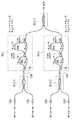
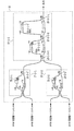
- FIG. 33 shows the configuration of a format variable modulator manufactured as the first embodiment.
- M 4
- the configuration of the distribution unit is a simple MZI type of the distribution unit type 1
- the configuration of the aggregation unit is a variable coupler type of the aggregation unit type 1
- the optical modulator The array unit has a basic configuration of a nested MZI type QPSK modulator. Therefore, the present modulator can be used as three types of modulators: 4-carrier QPSK modulation, 2-carrier 16 QAM modulation, and 1-carrier 256 QAM modulation.
- This modulator was realized by using a composite integrated technology (Non-Patent Document 3) in which a quartz-based planar lightwave circuit (PLC) and an LN modulation array are combined. Since the PLC waveguide has a very small EO effect and cannot constitute a high-speed modulator alone, the propagation loss is one-tenth or less of that of the LN waveguide and is a very low-loss waveguide medium. In addition, since the allowable bending radius of the bent waveguide is about 2 mm and the design flexibility is high, various optical circuits with low loss can be realized if the circuit is a passive circuit.
- PLC quartz-based planar lightwave circuit
- the LN waveguide has a large propagation loss and allowable bending radius compared to the PLC waveguide, so that it is not suitable to construct a complicated optical circuit, but has a high EO effect and also absorbs light due to modulation. Since this phenomenon does not occur, it is very excellent as a high-speed modulation circuit.
- a PLC waveguide is used for a passive circuit portion such as a distribution / aggregation circuit, and both are combined using an LN waveguide only for the modulation array portion.
- each TILF has a two-stage configuration, that is, the output of the main TILF 27-1-1-1, 27-2-1-1, 27-2-2-1, and the sub-TILF 27-1- 1-2, 27-1-1-3, 27-2-1-2, 27-2-1-3, 27-2-2-2, and 27-2-2-3 are connected.
- the sub-TILF and the main TILF basically have the same configuration, and the optical path length difference ⁇ L of the interferometer, that is, the FSR is the same.
- the sub-TILF has a configuration of one input and one output and is used as a so-called gate circuit. With such a configuration, the crosstalk leaked without being completely separated by the main TILF can be blocked by the sub-TILF, so that a separation characteristic at a low crosstalk can be obtained.
- TILF 27-1-1-1, 27-1-1-2, 27-1-1-3 As an example. If the carrier interval is ⁇ f, the FSRs of the TILFs 27-1-1-1, 27-1-1-2, and 27-1-1-3 are all designed to be 2 ⁇ f.
- TILF 27-1-1-1 to 27-1-1-3 as demultiplexers, that is, when separating the carrier light f1, f2, f3, f4 into two groups of f1, f3 and f2, f4 TILF27-1-1-1 is operated as a normal duplexer.
- variable optical phase shifter in the TILF 27-1-1-1 is adjusted so that f1 and f3 are output to, for example, the upper port and f2 and f4 are output to the lower port.
- the TILF 27-1-1-2 connected to the upper port has a variable optical phase shift in the TILF 27-1-2 so that f1 and f3 are maximum transmission and f2 and f4 are minimum transmission.
- the vessel has a variable optical shift in the TILF 27-1-1-3 so that f1 and f3 have minimum transmission and f2 and f4 have maximum transmission. Adjust the phaser.
- the carrier light separated by the TILF 27-1-1-1 is filtered by the TILF 27-1-1-2 and the TILF 27-1-1-3 to further remove unnecessary carrier light. Therefore, the two-stage TILF can obtain an extinction ratio that is twice as high as that of a normal one-stage structure, that is, a low crosstalk performance.
- variable optical phase shifter in the TILF 27-1-1-1-1 is used.
- the transmission characteristics of the TILF 27-1-1-1 are shifted on the frequency axis so that the transmittance to both output ports of the TILF 27-1-1-1 is the same at the frequency f1.
- the TILF 27-1-1-2 and the TILF 27-1-1-3 both have the maximum transmission at the frequency f1, and the TILF 27-1-1-2 and the TILF 27-1-1- 3 adjust each variable optical phase shifter.
- any branching ratio other than equal distribution for example, 2: 1.
- the branching ratio of TILF27-1-1-1 is basically the same as the desired branching ratio at frequency f1, for example 2: 1.
- the variable optical phase shifter in the TILF 27-1-1-1 is adjusted so that TILF 27-1-1-2 and TILF 27-1-1-3 are adjusted so as to achieve maximum transmission at the frequency f1, as in the case of equal distribution.
- TILF27-2-1-1, 27-2-1-2, 27-2-1-3, and TILF27-2-2-1, 27-2-2-2, 27-2-2-3 the idea is basically the same.
- TILF 27-2-1-1, 27-2-1-2, 27-2-1-3, 27-2-2-1, 27-2-2-2, 27-2-2-3 Both FSRs are designed to be 4 ⁇ f.
- the longer side of the optical path length of the TILF interferometer is the lower side with respect to TILF 27-1-1-1, 27-1-1-2, 27-1-1-3, For TILF27-2-1-1, 27-2-1-2, 27-2-1-3, 27-2-2-1, 27-2-2-2, 27-2-2-3 It has become. This is because the layout of these interferometers is actually arranged in ninety-nine folds on the circuit chip, so that the long side of these interferometers is always outside the ninety-nine folds. Because it is. By laying out in this way, the chip size can be reduced.
- thermo-optic phase shifter in the TILF uses a thermo-optic phase shifter.
- the thermo-optic phase shifter locally controls the temperature of the waveguide by a thin film heater provided on the waveguide clad, and controls the refractive index of the waveguide just below the thin film heater, that is, the phase of the guided light by the thermo-optic effect.
- a polarization maintaining fiber is connected to the input port.
- the 3 dB optical coupler which comprises each TILF was made into the wavelength independent coupler (WINC) design.
- the optical modulator array includes four nested MZI modulators (QPSK modulators) 1-1 to 1-4.
- QPSK modulators QPSK modulators
- FIG. 33 a modulation optical phase shifter that performs data modulation with a QPSK modulator is fabricated on an LN substrate, and a 3 dB optical coupler and variable optical phase shifters 12-4-1 to 12-12 for performing bias control.
- -4-16, and variable optical phase shifters 12-3-12-1 to 3-8 for adjusting the relative phase of the output light from each child MZI are provided on a PLC chip (PLC-I or PLC-O). Have been made.
- PLC-I or PLC-O PLC chip
- These variable optical phase shifters also use thermo-optic phase shifters.
- variable optical phase shifters 12-4-1 to 12-4-16 and the variable optical phase shifters 12-3-1 to 12-3-8 are provided on the PLC-O side this time, the PLC- Of course, it may be provided on the I side.
- the 3 dB optical coupler constituting the child MZI of the QPSK modulator and the 3 dB optical coupler on the input side of the parent MZI are constituted by Y branch waveguides.
- the 3 dB optical coupler on the output side of the parent MZI was a wavelength independent coupler (WINC).
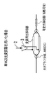
- the output of this WINC has 2 ports, but one is connected to the variable coupler VC which is an aggregation unit, and the other is the monitor output. Since this monitor is prepared for each QPSK modulator, it can be used as a monitor for adjusting the operating point bias of each QPSK modulator and adjusting the phase between Ich / Qch. Furthermore, since the output port of the distributing unit is being monitored though the QPSK modulator, it can be used as a TILF demultiplexing state or a branching ratio monitor when the TILF is operated as a coupler. it can. By using this monitor, these adjustments can be performed very efficiently compared to the case of monitoring signal light from the output port.
- variable optical phase shifters 12-1-1 and 12-1-2 and the variable optical phase shifters 12-2-1 to 12-2-4 shown in FIG. 27 are omitted, the QPSK modulation of FIG.
- the variable optical phase shifters 12-3-1 to 12-3-8 in the device can be used in combination for driving. For example, when the phase corresponding to the variable optical phase shifter 12-2-1 is to be moved by ⁇ , the variable optical phase shifters 12-3-1 and 12-3-2 located upstream thereof may be simultaneously moved by ⁇ .
- variable phase shifter 12-2-1 In effect, the phase is moved by ⁇ by the variable phase shifter 12-2-1.
- variable optical phase shifters 12-3-1 and 12-3-2 When the variable optical phase shifters 12-3-1 and 12-3-2 are originally set to ⁇ 1 and ⁇ 2 , respectively, they may be reset to ⁇ 1 + ⁇ and ⁇ 2 + ⁇ , respectively.
- the variable optical phase shifters 12-3-1 to 12-3-4 located upstream thereof may be simultaneously moved by ⁇ .
- the circuit length is shortened by eliminating the variable optical phase shifter.
- variable couplers VC25-1-1, 25-2-1 and 25-2-2 are Mach-Zehnder interferometers (MZI) in which two 3 dB optical couplers are connected via a variable optical phase shifter. These variable optical phase shifters also use thermo-optic phase shifters.
- the 3 dB optical coupler was a normal directional coupler. In the case of a normal directional coupler, the coupling rate has a certain wavelength dependence.
- the directional coupler is wavelength-dependent and the coupling ratio is deviated from 3 dB, that is, 50%, in general, no matter how the variable optical phase shifter is set, the overall VC has a high coupling ratio (for example, 1: 0). Etc.) cannot be obtained. However, this time, the required coupling ratio of these VCs is 1: 1 or 2: 1, and the ratio is not so large. Under such conditions, the wavelength dependency generally generated in the directional coupler is at a level that does not cause a problem in the communication wavelength band (1520 to 1620 nm), so that the normal direction in which a small size and low loss characteristics can be obtained. The sex coupler is used this time.
- the PLC chip was manufactured using a combination of a glass film deposition technique such as a flame deposition (FHD) method and a fine processing technique such as reactive ion etching (RIE). Specifically, a glass film serving as a lower cladding layer was deposited / transparent on a silicon substrate, and subsequently a core layer having a refractive index slightly higher than that of the cladding layer was deposited. Then, a core pattern to be an optical waveguide circuit was patterned by a microfabrication technique, and a glass film to be an upper clad layer was deposited / transparent to produce a buried optical waveguide. Finally, a metal to be a thin film heater was deposited on the surface of the upper clad by a vacuum deposition method or the like, patterned with a fine processing technique, and loaded with a thermo-optic phase shifter.
- a glass film deposition technique such as a flame deposition (FHD) method
- RIE reactive ion etching
- the relative refractive index difference between the core and clad of the waveguide is 1.5%.
- the chip size was about 14 ⁇ 36 mm for PLC (I) and about 7 ⁇ 31 mm for PLC (O).
- an electric wiring pattern for supplying driving continuous current to each thin film heater is formed on the chip.
- the LN chip is composed of a total of 16 phase modulation arrays of 2 to 8 sets formed on an X-cut substrate.
- Each waveguide of the phase modulation array is manufactured by a titanium diffusion method, and as shown in FIGS. 3A and 3B, a center electrode is formed at the upper part between each pair of waveguides, and a GND electrode is formed around each pair. Thus, a traveling wave electrode is formed.
- FIG. 33 As shown in FIGS. 3A and 3B, high-frequency wiring patterns for propagating modulation signals to the traveling wave electrodes are formed on the chip.
- these PLC chips and LN chips are connected to the end faces, and polarization maintaining optical fibers and ordinary single mode optical fibers are connected to the input port of PLC-I and the output port of PLC-O, respectively.
- the entire chip was housed and mounted in a high frequency package.
- a multi-subcarrier light source composed of four wavelength variable light source arrays shown in FIG. 9B and an optical coupler was connected to the manufactured modulator, and the modulation operation was confirmed.
- the light emission frequency interval of each wavelength variable light source, that is, the subcarrier interval is 25 GHz.
- Eight PN 11 stages of pseudo-random (PRBS) NRZ electric signals were input to the eight modulation optical phase shifter center electrodes for performing data modulation with different delays.
- the modulation symbol rate is 25 Gbaud. Therefore, since the subcarrier interval is equal to the symbol rate, the optical signal generated by this modulator using a plurality of subcarrier lights is an OFDM signal.
- TILF27-1-1-1-1 is a demultiplexer that divides these subcarrier lights into two groups, f1 and f3 to TILF27-1-1-2, and f2 and f4 to TILF27-1-1-3. Make it work.
- TILF27-1-1-2 operates as a filter that transmits f1 and f3, and blocks f2 and f4.
- TILF27-1-1-3 transmits f2 and f4, and f1 and f3. And act as a filter that shuts off.
- the TILF 27-2-1-1 operates as a demultiplexer for dividing f1 and f3, f1 to the TILF 27-2-1-2 side, and f3 to the TILF 27-2-1-3 side.
- TILF 27-2-1-2 operates as a filter that transmits and blocks f3 with respect to f1
- TILF 27-2-1-3 operates as a filter that transmits and blocks f3.
- TILF27-2-2-1 operates as a demultiplexer for dividing f2 and f4, f2 to the TILF27-2-2-2 side, and f4 to the TILF27-2-2-3 side.
- the TILF 27-2-2-2 operates as a filter that transmits f2 and blocks f4, and the TILF 27-2-2-3 operates as a filter that transmits f4 and blocks f2.
- the four QPSK modulators 1-1 to 1-4 are each operated as a QPSK modulator.
- VC25-1-1, 25-2-1 and 25-2-2 all adjust to 50% binding. If there is a variation in actual device propagation loss or a variation in the optical power level of each subcarrier light, the coupling rate of these VCs is finely adjusted so that the level of each subcarrier signal is aligned. Again, of course.
- the optical spectrum of the output signal light is shown in the upper part of FIG. 34A.
- the spectrum of the output signal light when the subcarrier is caused to emit light one wave at a time using the multicarrier light source is also shown.
- the signal constellation of the output signal light when the subcarriers emit light one wave at a time that is, the signal constellation of each subcarrier is shown in the lower part of FIG. 34A.
- 2-subcarrier lights f1 and f2 are input from the multi-subcarrier light source to the modulator.
- the TILF 27-1-1-1 operates as a demultiplexer that divides these subcarrier lights, f1 into the TILF 27-1-1-2 side, and f2 into the TILF 27-1-1-1 side.
- the TILF 27-1-1-2 operates as a filter that transmits and blocks f2 with respect to f1
- the TILF 27-1-1-3 operates as a filter that transmits and blocks f2 with respect to f2.
- the TILF 27-2-1-1 operates to become a 2: 1 coupler at f1.
- Both TILFs 27-1-2-2 and 27-2-1-3 are operated so as to have maximum transmission with respect to f1.
- the TILF 27-2-2-1 operates to become a 2: 1 coupler at f2.
- the TILFs 27-2-2 and 27-2-2-3 are operated so as to have maximum transmission with respect to f2.
- the QPSK modulator operates as a 16QAM modulator by combining the QPSK modulators 1-1 and 1-2 and the QPSK modulators 1-3 and 1-4, respectively.
- VC25-1-1 adjusts to 50% binding.
- VC25-2-1 and 25-2-2 are adjusted to be 2: 1 couplers.
- Relative relationship between a QPSK signal (large QPSK signal) generated by the QPSK modulator 1-1 and a QPSK signal (small QPSK signal) generated by the QPSK modulator 1-2 The phase relationship is adjusted by changing the variable optical phase shifters 12-3-1 and 12-3-2 simultaneously or by changing the variable optical phase shifters 12-3-3 and 12-3-4 simultaneously.
- the variable optical phase shifters 12-3-5 and 12-3-6 are simultaneously used.
- adjustment is performed by changing the variable optical phase shifters 12-3-7 and 12-3-8 at the same time.
- FIG. 34B shows the optical spectrum of the output signal light and the signal constellation of each subcarrier.
- the TILF 27-1-1-1 operates to become a 4: 1 coupler at f1. Both TILFs 27-1-1-2 and 27-1-1-3 are operated so as to have maximum transmission with respect to f1. Both TILF27-2-1-1 and TILF27-2-2-1 are operated so as to be 2: 1 couplers at f1. The TILFs 27-2-1-2, 27-2-1-3, 27-2-2-2, and 27-2-2-3 are all operated so as to have maximum transmission with respect to f1.
- the QPSK modulator operates as a 256 QAM modulator by combining four QPSK modulators.
- VC25-1-1 is adjusted to be a 4: 1 coupler
- VC25-2-1 and 25-2-2 are adjusted to be a 2: 1 coupler.
- the relative phase relationships between the QPSK signals generated by the QPSK modulators are variable optical phase shifters 12-3-1 and 12-3-2, 12-3-3 and 12-3-4, 12-3-. Adjustment is made by changing 5 and 12-3-6 and 12-3-7 and 12-3-8 as a set.
- the optical spectrum of the output signal light was almost the same as the spectrum of only ch1 in the upper diagram of FIG. 34B.
- the signal constellation a figure considered to be a signal point of 16 rows and 16 columns was obtained, but when it becomes a 256 QAM signal, the quality of the drive electric signal itself, that is, the influence of noise becomes visible, so that the blurred constellation is visible. It became the adjustment. Since this is not a fundamental problem, it can be improved by operating in an evaluation system that improves the quality of the drive electrical signal itself.
- signal lights having different numbers of carriers and multi-values that is, signal lights of a plurality of modulation formats having different occupied bandwidths and SNR degradation tolerances can be dynamically switched and generated by the same modulator. did it.
- Example 2 As a modified version of Example 1, the configuration of the aggregation unit is the configuration of the aggregation unit embodiment 6 in Example 2. The configuration of this consolidating unit is shown in FIG. The configurations and operations of the distribution unit and the optical modulator array unit are the same as those in the first embodiment.
- This aggregating unit uses a configuration in which the distributing unit form 6 and the distributing unit form 7 are combined as an aggregating unit by switching input / output.
- the first stage TILFs 57-2-1 and 57-2-2 use the variable coupler built-in simple MZI type TILF shown in the distribution unit form 6, and the final stage TILF 57-1-1 has a distribution unit.
- the lattice type built-in TILF shown in the seventh embodiment is used.
- the concept of the basic operation of these TILFs is the same as that described in the distribution unit form 6 and the distribution part form 7, and the branching / demultiplexing may be read as combining / combining, respectively.
- the TILF 57-2-1 is a multiplexer that combines the signal light of the carrier frequency f1 from the QPSK modulator 1-1 and the signal light of the carrier frequency f3 from the QPSK modulator 1-2
- TILF 57-2 -2 is a multiplexer that combines the signal light of the carrier frequency f2 from the QPSK modulator 1-3 and the signal light of the carrier frequency f4 from the QPSK modulator 1-4
- TILF57-1-1 is the TILF57-2- 1 is operated as a multiplexer that combines the signal light of carrier frequencies f1 and f3 from 1 and the signal light of carrier frequencies f2 and f4 from TILF 57-2-2.
- the TILF 57-2-1 combines the signal light of the carrier frequency f1 from the QPSK modulator 1-1 and the signal light of the carrier frequency f1 from the QPSK modulator 1-2 at a ratio of 2: 1 to generate a 16QAM signal.
- TILF57-2-2 combines the signal light of the carrier frequency f2 from the QPSK modulator 1-3 and the signal light of the carrier frequency f2 from the QPSK modulator 1-4 at a ratio of 2: 1.
- TILF57-1-1 operates as a combiner that combines the signal light of carrier frequency f1 from TILF57-2-1 and the signal light of carrier frequency f2 from TILF57-2-2
- the TILF 57-2-1 combines the signal light of the carrier frequency f1 from the QPSK modulator 1-1 and the signal light of the carrier frequency f1 from the QPSK modulator 1-2 at a ratio of 2: 1 to generate a 16QAM signal.
- TILF57-2-2 combines the signal light of the carrier frequency f1 from the QPSK modulator 1-3 and the signal light of the carrier frequency f1 from the QPSK modulator 1-4 at a ratio of 2: 1.
- a combiner for combining 16QAM signals the TILF57-1-1 combines the signal light of the carrier frequency f1 from the TILF57-2-1 and the signal light of the carrier frequency f1 from the TILF57-2-2 at a ratio of 4: 1. It operates as a combiner that combines 256QAM signals.
- a simple MZI type with a built-in variable coupler is used for TILFs 57-2-1 and 57-2-2, and a lattice type TILF with a built-in variable coupler is used for TILF57-1-1.
- TILF57-1-1 is better to have a sharp filter characteristic in order to interleave and multiplex even and odd channels alternately. Therefore, a TILF with a variable coupler with built-in variable coupler that has excellent rectangularity of transmission frequency characteristics can be used. Using.
- the adjacent channel is not multiplexed, but the channel skipped by 1 channel is multiplexed.
- a simple MZI type TILF with a built-in variable coupler that can be small was used.
- the circuit configuration of the aggregation unit is slightly more complicated than that in the first embodiment, but in the case of multicarrier, the loss is low and crosstalk caused by signal harmonics is generated between the carrier signals. The advantage of less is obtained.
- TILF57-1-1 plays a major role. This is because the influence of the crosstalk from the signal of the adjacent channel is the largest as described in the aggregation unit form 5. Therefore, if it is not necessary to consider the loss so much, TILFs other than the final stage, in this embodiment, TILFs 57-2-1 and 57-2-2 are used by using the variable optical coupler shown in the aggregation unit form 1. Also good. In this case, loss is sacrificed during some multiplexing operations, but the circuit size can be reduced by replacing TILF with a variable optical coupler. As described above, according to the required specifications, it is of course possible to employ a configuration in which the forms of the aggregation units are interwoven.
- FIG. 36 shows the configuration of a format variable modulator with a polarization multiplexing function manufactured as the third embodiment.
- M 4
- the configuration of the distribution unit is the simple MZI type of the form 1
- the configuration of the aggregation unit is the variable coupler type of the aggregation unit form 1
- the optical modulator array unit Has a basic configuration of a single MZI type BPSK modulator, and two systems are integrated to perform polarization multiplexing.
- the present modulator can be used as three types of modulators: polarization multiplexed 4-carrier BPSK modulation, polarization multiplexed 2-carrier QPSK modulation, and polarization multiplexed 1-carrier 16 QAM modulation.
- This modulator was also realized by applying a composite integration technique that combines a quartz-based planar lightwave circuit (PLC) and an LN modulation array.
- PLC quartz-based planar lightwave circuit
- LN chip substrate is also an X-cut substrate as in the first embodiment.
- each TILF of the distribution unit has a two-stage configuration in which low crosstalk characteristics can be obtained as in the first embodiment.
- the two-stage configuration is collectively labeled as TILF.
- the optical coupler that distributes the CW input light to the two systems is arranged after the distributing unit, that is, before the optical modulator array, not before the distributing unit.
- the input light is immediately input to the distribution unit composed of TILF, and after being demultiplexed or branched by this distribution unit, it is distributed by the four distribution couplers and input to the BPSK modulator.
- the eight BPSK modulators are BPSK modulators 50-1, 50-3, 50-5, 50-7 for X polarization, BPSK modulators 50-2, 50-4, 50-6, 50-8. Are alternately arranged for Y polarization, X polarization signal and Y polarization signal from above.
- both the modulator for the X polarization signal and the modulator for the Y polarization signal are modulators using the X cut substrate, the signal light at the time of passing through these modulators is horizontal with respect to the substrate. Note that it propagates in a different polarization direction (TE polarization). These signals are combined or combined by a combining 3 dB coupler or VC, and then the polarization signal is converted into a direction perpendicular to the substrate (TM polarization) by the polarization rotator. Then, the signal is multiplexed with the other X-polarized signal light and output by the polarization combining coupler.
- TE polarization polarization direction
- an optical coupler that distributes the input CW light to two systems for the X polarization signal and the Y polarization signal (each polarization signal distribution 3 dB optical coupler) is provided between the distribution unit and the optical modulator array unit.
- the distribution unit can be shared for the X polarization signal and the Y polarization signal, and the number of distribution units can be suppressed to only one set.
- the area of the distribution section made up of TILF or the like is many orders of magnitude larger, so the layout area can be greatly reduced.
- the TILF of the distribution unit operates a plurality of variable phase shifters as described above, but the fact that only one set of distribution units is required does not increase the number of operation points. This means that operation control can be simplified and the power consumption can be reduced.
- the aggregation unit is laid out so that two circuits for the X polarization signal and the Y polarization signal are woven.
- the variable optical coupler VC25-1 outputs the modulated signal light for X polarization
- the variable optical coupler VC25-2 outputs the modulated signal light for Y polarization, which passes through the polarization rotator and the polarization combining coupler. These signal lights are polarization multiplexed and output.
- a method other than the method of FIG. 31A is also possible as a method of laying out two systems of optical circuits for X polarization signal and Y polarization signal.
- the BPSK modulators 50-1 to 50-4 are used for the X polarization signal and the BPSK modulators 50-5 to 50-8 are used for the Y polarization signal.
- the outputs of the distribution optical couplers are knitted together and connected to these BPSK modulators, and the X polarization signal aggregation unit and the Y polarization signal aggregation unit are simply arranged vertically.
- FIG. 37 shows a layout in which the outputs of the distribution optical couplers are knitted together and connected to these BPSK modulators, and the X polarization signal aggregation unit and the Y polarization signal aggregation unit are simply arranged vertically.
- the BPSK modulators 50-1, 50-2, 50-5, and 50-6 are used for the X polarization signal
- the BPSK modulators 50-3, 50- 4, 50-7 and 50-8 are used for the Y polarization signal
- the outputs of the distribution optical couplers 49-1 and 49-2 are knitted
- the outputs of the distribution optical couplers 49-3 and 49-4 are knitted.
- the X polarization signal aggregating unit and the Y polarization signal aggregating unit have a layout that is knitted only between the joining 3 dB optical coupler and the VC. In either method, the order of arrangement of the BPSK modulator for the X polarization signal and the BPSK modulator for the Y polarization signal only changes, and the connection relationship as an optical circuit does not change.
- the lengths of the waveguides to each polarization signal distribution 3 dB optical coupler and each BPSK modulator appear to be different in each path in the drawing, but in the actual layout, they are the same length.
- the path length of the TILF is calculated on the short arm side, and the distance from the input port to the output port of the modulator is designed to be the same for each path for each BPSK modulation.
- this isometric design is applied to the configurations shown in FIG. 36 of the first and second embodiments and the third embodiment.
- a thin film half-wave plate whose main axis is inclined by 45 ° is used for a polarization rotator that converts TE polarized light into TM polarized light.
- each polarized light passing through the 45 ° half-wave plate is polarized and converted to a position half-rotated by the PQ axis which is a 45 ° linear polarization axis. Therefore, TE polarized light is converted to TM polarized light, and TM polarized light is converted to TE polarized light, so that it operates as a TE / TM converter.
- the half-wave plate is inserted into a groove crossing the waveguide and fixed with an adhesive that matches the refractive index.
- the groove crossing the waveguide is formed by tilting it by 8 degrees in order to prevent reflection on the half-wave plate from propagating as return light.
- the angle of the polarization-maintaining input fiber is adjusted so that the signal light input to the PLC-I becomes TE polarized light.
- the polarization combining coupler uses an interferometer in which a stress release groove is dug in one of two arm waveguides sandwiched between two optical couplers. Quartz-based waveguides that have undergone a high-temperature transparency process for glass generally generate a strong compressive stress due to the difference in thermal expansion coefficient between the silicon substrate and the quartz glass, resulting in birefringence B. Since the birefringence B has a very small value due to stress release in the stress release groove, a polarization combining coupler is constructed by adjusting the length of the stress release groove and the waveguide length difference of the interferometer.
- the optical path length difference of the interferometer arm in use can be designed to be, for example, an equal length optical path length difference for TE polarized light and a half wavelength optical path length difference for TM polarized light.
- TE polarized light and TM polarized light propagate to different ports, both the TE polarized signal light input to the upper input port and the TM polarized light input to the lower input port are both output ports. Can be output. Accordingly, such an interferometer operates as a polarization combining coupler.
- thermo-optic phase shifter used as a variable optical phase shifter is provided with a heat insulating groove for reducing the power consumption of the thermo-optic phase shifter (not shown in FIGS. 36 to 38).
- an electric wiring pattern for supplying driving continuous current to each thin film heater is formed on the chip.
- the modulation operation was confirmed using the multicarrier light source shown in FIG. 9B.
- the light emission frequency interval of each wavelength variable light source that is, the carrier interval was set to 50 GHz.
- Eight PN 11 stages of pseudo-random (PRBS) NRZ electric signals were input to the eight modulation optical phase shifter center electrodes for performing data modulation with different delays.
- the modulation symbol rate is 25 Gbaud. Therefore, since the carrier interval is twice the symbol rate, the optical signal whose operation is confirmed in this embodiment is a normal FDM signal.
- the current modulation symbol rate is set to 25 Gbaud for the convenience of the evaluation device.
- the modulation symbol rate is increased to 50 Gbaud as an OFDM signal as described above, the signal of each carrier Since independence can be maintained, for example, it is of course possible to perform modulation at a symbol rate of 32 Gbaud used in 100 G transmission.
- TILF 27-1-1 When a 4-carrier BPSK modulation signal is generated, 4-carrier lights f1, f2, f3, and f4 are input from the multicarrier light source to the modulator.
- the TILF 27-1-1 transmits these carrier lights to f1, f3 to the TILF 27-2-1 side, and f2 and f4 to the two groups to the TILF 27-2-2 side.
- TILF27-2-1 is operated as a demultiplexer
- TILF27-2-1 is operated as a demultiplexer
- f1 and f3 are divided into the distribution 3 dB coupler 49-1 side
- f3 is distributed to the 3 dB coupler 49-2 side.
- the TILF 27-2-2 operates as a demultiplexer that divides f2 and f4, f2 into the distributing 3 dB coupler 49-3 side, and f4 into the distributing 3 dB coupler 49-4 side.
- Each of the eight BPSK modulators is operated as a BPSK modulator. Both VC25-1 and VC25-2 are adjusted to 50% binding.
- the 2-carrier light f1, f2 is input from the multicarrier light source to the modulator.
- the TILF 27-2-1 is operated to be a 3 dB coupler at f1
- the TILF 27-2-2 is operated to be a 3 dB coupler at f2.
- the BPSK modulator includes BPSK modulators 50-1 and 50-3, BPSK modulators 50-2 and 50-4, BPSK modulators 50-5 and 50-7, and BPSK modulators 50-6 and 50-8, respectively.
- the set is operated as a QPSK modulator. Both VC25-1 and VC25-2 are adjusted to 50% binding.
- FIG. 32B shows the optical spectrum of the X polarization signal of the output signal light and the signal constellation of each subcarrier. Similar measurement results were obtained for Y polarization. Thus, it can be seen that a good polarization multiplexed 2-carrier QPSK modulated signal can be generated.
- TILF 27-1-1 When 1-carrier 16QAM modulation is generated, only the carrier light f1 is input from the multicarrier light source to the modulator.
- the TILF 27-1-1 operates to become a 2: 1 coupler at f1
- the TILF 27-2-1 and TILF 27-2-2 operate to become a 3 dB coupler at f1.
- Two sets of BPSK modulators, one set of four BPSK modulators 50-1, 50-3, 50-5 and 50-7, and one set of 50-2, 50-4, 50-6 and 50-8 As a 16QAM modulator.
- VC25-1 and VC25-2 are adjusted to be 2: 1 couplers.
- QPSK signal (large QPSK signal) generated by a QPSK modulator composed of BPSK modulators 50-1 and 50-3, and BPSK modulators 50-5 and 50-7
- the relative phase relationship of the QPSK signal (small QPSK signal) generated by the QPSK modulator with the electric field strength of 1 is the same as that of the variable optical phase shifters 12-1 and 12-3 or the variable optical phase shifter 12- Adjust by changing 5 and 12-7 simultaneously.
- a large QPSK signal generated by a QPSK modulator composed of BPSK modulators 50-2 and 50-4 and a small QPSK modulator composed of BPSK modulators 50-6 and 50-8.
- the relative phase relationship of the QPSK signal is adjusted by changing the variable optical phase shifters 12-2 and 12-4 simultaneously or by changing the variable optical phase shifters 12-6 and 12-8 simultaneously.
- FIG. 39C shows the optical spectrum of the X polarization signal of the output signal light and the signal constellation of each subcarrier. Similar measurement results were obtained for Y polarization. Thus, it can be seen that a good polarization multiplexed 1-carrier 16QAM modulated signal can be generated.
- signal lights having different numbers of carriers and multi-values that is, signal lights of a plurality of modulation formats having different occupied bandwidths and SNR degradation tolerances are dynamically switched by the same modulator.
- signal lights having different numbers of carriers and multi-values that is, signal lights of a plurality of modulation formats having different occupied bandwidths and SNR degradation tolerances are dynamically switched by the same modulator.
- the birefringence adjustment using the stress release groove is used to realize the polarization beam combiner.
- a flat waveguide structure with a wider waveguide width in the lateral direction is used, or a method that utilizes the birefringence of the half-wave plate itself by inserting the half-wave plate into the waveguide at an angle of 0 ° or 90 ° of the principal axis Also good.
- a normal 3 dB optical coupler may be substituted if a 3 dB principle loss is allowed.
- polarization combiner can avoid this principle loss, and the polarization component that could not be rotated by the polarization rotator can be removed by the polarization combiner, reducing polarization crosstalk. Because of this, it is usually better to use a polarization beam combiner.
- an X-cut substrate is used for the LN chip, but a configuration using a Z-cut substrate may be used.
- the number of signal electrodes is doubled compared to the case where an X-cut substrate is used.
- a Z-cut substrate having a domain-inverted structure may be used.
- the number of signal electrodes may be the same as when an X-cut substrate is used.
- the combination of the LN waveguide and the silica-based PLC waveguide is described as a combination of composite integration, but this is because the LN waveguide has a high EO effect and is the mainstream guide of a high-speed modulator. This is because it is a waveguide technology, and a quartz-based waveguide is the waveguide with the lowest loss as a passive waveguide, and this combination is excellent as a combination for realizing a complex modulator with low loss.
- the modulator components can be realized by a spatial device, it may be configured by a spatial device.
Landscapes
- Physics & Mathematics (AREA)
- Electromagnetism (AREA)
- Engineering & Computer Science (AREA)
- Computer Networks & Wireless Communication (AREA)
- Signal Processing (AREA)
- Optics & Photonics (AREA)
- Nonlinear Science (AREA)
- General Physics & Mathematics (AREA)
- Optical Modulation, Optical Deflection, Nonlinear Optics, Optical Demodulation, Optical Logic Elements (AREA)
Abstract
Description

図7に、本発明の第1の実施形態であるフォーマット可変光変調器の構成を示す。本形態の変調器構成は、可変1×2ILFを多段に接続して構成した可変1×M分波フィルタ24と、M個の位相変調器(PSK変調器)13-1~13-4とM/2個の2入力1出力光カプラ7g、7hと(M/2)入力1出力可変光カプラ25とからなる。図7はM=4の例を示している。

次に、Mが2の累乗以外の場合、例えばM=12の場合の構成について図14に示す。本構成はM=16の構成を基に一部の構成要素を省いた構成になっている。具体的には、4段目のTILF27-4-1~27-4-4、及び1段目のVC25-4-1~25-4-4がM=16ではそれぞれ8個並ぶが本構成では4個になっており、また、光変調アレイも16個から12個に削減した構成になっている。このように一部の要素を減らす構成とすることで、対応するキャリア数も減ることとなる。尚、当然のことながら図中の各TILFの光路長差の基本単位ΔLは、前述の式でM=16とした時の値である。具体的な各種信号フォーマットを発生するための動作状態の例を図15AおよびBの表に示す。図15AおよびBで1つの表を示す。尚、表の中において、各符号の名称TILF/VCの1-1~4-4、PSK1~12は図14の中で示している名称で記載している。本変調器では、12キャリアBPSK信号、6キャリアQPSK信号、3キャリア16QAM信号、2キャリア64QAM信号、1キャリア4096QAM信号の5種類の信号を切り替えて発生することができる。尚、表では1キャリア4096QAM信号に関しては省略している。また、第1の実施形態で説明したように、一部のフォーマットでは複数の動作モードがある場合があるが、本表では代表的な動作モードのみ記載している。
次に、分配部の様々な構成について説明する。以下、M=4の場合で具体的に示すが、M=4以外の場合でも基本的には同様であることを予め断っておく。
図16Aは、分配部形態1として、第1の実施形態;M=4での分配部の構成を改めて詳しく説明した図である。TILF27-1-1~27-2-2のそれぞれは2個の2入力2出力の3dB光カプラ7a~7fに可変光移相器12a~12f付きの遅延線が挟まれたMZI構成になっている。TILF27-1-1の遅延線の光路長差は2ΔL、TILF27-2-1、27-2-2での光路長差はΔLになっている。分離するキャリアの周波数間隔がΔfの場合、ΔL=c/(M・Δf)である。cは光速である。ここで、光カプラ7a~7fは全て2入力2出力の構成で、入力側光カプラの一方の入力を未接続としたが、入力側の光カプラは1入力2出力の構成としても良い。また、光カプラの具体的な実現方法は、方向性結合器やマルチモード導波路構成、又は、波長無依存カプラ(WINC)と呼ばれる一種の干渉計など、いずれの方法を用いても良く、1入力2出力構成の場合はY分岐を用いても良い。以降で述べる形態に関しても同様である。
図18は、分配部形態2として、分配部のTILFをラティス型の干渉計で構成した例である。ラティス型の干渉計は、非特許文献4、5で開示されているように、MZIを多段にラティス状に接続した構成となっており、各段のMZIの位相状態、及びカプラの結合率を個別に設定できることから、ラティスの段数を増やせば増やすほど透過特性の設計自由度が大きくなるという利点がある。一方、回路長がラティスの段数に応じて長くなる点が欠点である。ここでは、分配部形態1の単純MZI型との特徴の差を簡単に示す為に、ラティス段数が2段の例で動作を説明する。図中にも記載しているが、TILF27-1-1の光路長差は、入力側に近い1段目がΔL、出力側に近い2段目が2ΔLであり、TILF27-2-1、27-2-2の光路長差は1段目が2ΔL、2段目が4ΔLである。尚、光路長差の基本単位ΔLは、単純MZIの場合と同じである。
図20は、分配部形態3として、分配部を非特許文献6に記載のM分波のFFT型干渉計で構成した例である。FFT型の干渉計は1入力M分岐カプラ39に、ΔLずつ遅延差を持つM本の遅延線アレイ40、及び2入力2出力カプラ7d~7gと可変光移相器12a~12hを編みこんで接続構成した多段の可変M×Mカプラ41からなる。図20では1入力M分岐カプラ39は1入力2出力光カプラ7a~7cを多段に接続して構成しているが、1入力M出力のMMIカプラ等を用いて構成しても良い。尚、遅延線部の光路長差の基本単位ΔLは、単純MZIの場合と同じである。

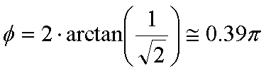
以上は、干渉計フィルタの干渉条件を変えることで、分配部を分波回路や可変分岐比光カプラとして切り替えて動作させる構成例を示してきたが、次にこれらとは別の考え方の構成方法を分配部形態4として図22に示す。本図はM=4の場合を示している。本分配部は、各箇所においてインターリーブフィルター(ILF)と可変光カプラ(VC)を光スイッチで選択できるよう構成されている。各ILFとVCを図11の表の動作に倣って単純に切り替えて使用することで、分配部の可変動作を実現する。分配部形態1~3の干渉計型フィルタのように細かな干渉条件の調整が不要になる点が利点であるが、光スイッチが必要となるので全体構成が複雑になる点が欠点である。尚、本構成も動作モードの限定によって常に結合率が3dBになるVCについては、VCを単純な3dBカプラに置き換えてももちろん良い。尚、光スイッチには、On/Off切り替えタイプの構成でも良いし、或いは、可変光カプラと同じ構成を用いて、中間領域を用いずに100%透過、0%透過の動作点を用いるようにしても良い。
更に別の構成を分配部形態5として図23に示す。本図もM=4の場合を示している。本構成では、可変光カプラ(VC)がツリー状に多段に接続され、且つ、各VCのいずれか一方の出力に2入力1出力光スイッチが挿入され、この光スイッチのVCが接続されていない側のポートが、分配部の入力ポートになっている。従って、初段目のVCの入力ポートと合わせてM入力(本図ではM=4)の回路になっている。本構成を分配部に用いる場合は、マルチキャリア光源は用いずにこの4入力に個別のキャリア光源を別々に接続する。4キャリア時は、4つのキャリア光源をそれぞれの波長で発光させ、全ての光スイッチを分配部の入力ポート側、即ち各キャリア光源側を選択するように切り替える。VC25-1-1、25-2-2も経路選択スイッチとして用い、入力ポート3からの光が出力ポート3に導かれるように設定する。同様にVC25-2-1も経路選択スイッチとして用い、入力ポート2からの光が出力ポート2に導かれるように設定する。2キャリア時は、入力ポート2、3のキャリア光源を発光させ、光スイッチ43-1-1のみ分配部の入力ポート側を選択するように設定し、光スイッチ43-2-1、43-2-2はVC側を選択するように設定する。VC25-1-1は経路選択スイッチとして用い、入力ポート3からの光がVC25-2-2に導かれるように設定する。VC25-2-1、25-2-2は3dBカプラとして動作するように設定する。1キャリア時は、入力ポート3のみキャリア光源を発光させ、全ての光スイッチがVC側を選択するように設定する。VC25-1-1は2:1カプラとして、VC25-2-1、25-2-2は3dBカプラとして動作するように設定する。このように動作させることで、各変調フォーマットを切り替えることができる。尚、本構成での光スイッチについても、On/Off切り替えタイプの構成を用いても良いし、或いは、2入力1出力可変光カプラと同じ構成を用いて、中間領域を用いずに100%透過、0%透過の動作点を用いるようにしても良い。
更に別の構成を分配部形態6として説明する。全体構成は分配部形態1、2と同じであるが、各TILFの構成がこれらとは異なる。本形態でのTILFの構成を図24Aに示す。本形態でのTILFは、2個の可変光カプラに可変光移相器付きの遅延線が挟まれたMZI構成になっている。各可変カプラは、本図では、2個の3dB光カプラを2個の可変光移相器を介して接続したMZI構成としたが、別の構成でも構わない。遅延線による2本の干渉アームの光路長差は、本図ではΔL=c/(M・Δf)の場合で図示しているが、M=4の場合のTILF27-1-1では2ΔL、TILF27-2-1、27-2-2ではΔLとなる。M=4以外も含めた一般構成では、n段目のTILF、即ちTILF27-(n)-(X)の光路長差はM・ΔL/2nになる。
更に別の構成を分配部形態7として説明する。本形態でのTILFの構成を図25Aに示す。本形態は、基本的には分配部形態2に分配部形態6の考えを適用したものであり、各TILFの構成が単MZIをベースとした構成ではなく、ラティス型干渉計をベースとした構成になっている点が分配部形態6での考えと異なる。本形態でのTILFは、可変光カプラと可変光移相器付きの遅延線が交互に接続された構成になっている。
更に別の構成を分配部形態8として説明する。M=4における、本分配部形態の構成を図26に示す。本形態は、分配部形態3に分配部形態6の考えを適用したものであり、分配部形態3のFFT型干渉計において、一部又は全ての光カプラを可変光カプラに置き換えている。また、分配部形態6で説明したように、分岐動作時の不要経路からのクロストークを低減する為に、FFT型干渉計の遅延線部分にOnOff光スイッチを挿入している。もし、クロストーク特性の向上が必要なければ、本OnOff光スイッチは省略することができる。本形態は、基本的には分配部形態3に分配部形態6の考えを適用したものであるので、メリット、デメリットはこれらに上げているものと基本的には同じである。
次に、集約部の様々な構成について説明する。以下、M=4の場合で具体的に示すが、M=4以外の場合でも基本的には同様であることを予め断っておく。
図27は、集約部形態1である可変カプラ型集約部の構成図である。本構成は、第1の実施形態での集約部の構成を一般化した構成になっている。可変光カプラ(VC)が逆ツリー状に多段に接続され、集約部の入力ポートと可変カプラの間や各可変カプラの間には可変光移相器が配置されている。この様な構成で集約部の各入力ポートからの光を任意の比率で、且つ任意の相対位相関係で出力ポートに合流させることができる。
図28は、集約部形態2の構成である。本形態は、可変カプラ型(集約部形態1)の可変カプラ部を、可変減衰器と2入力1出力光カプラの組み合せに置き換えたものになっている。本形態でも可変減衰器の減衰量を調整することで集約部の各入力ポートからの光を任意の比率で、且つ任意の相対位相関係で出力ポートに合流させることができる。但し、減衰によって比率を変えているので、等比率での合流以外の動作では原理的な損失が発生する。可変カプラ型(集約部形態1)ではこのような原理損失は発生しない。一方、本構成では、集約部の各入力ポートに対して個別に可変減衰器が備えられていることになるので、集約部の各入力ポートからの光のレベル調整が行いやすいという利点がある。
図29は、集約部形態3の構成である。本構成は、可変カプラ型と可変減衰器型を合わせた構成になっている。可変カプラにより合流比を調整することで原理損失を抑えると同時に、集約部の各入力ポートからの光のレベル調整も行いやすくなっている。欠点は、回路の規模が大きくなることである。
図30は、集約部形態4の構成である。本構成は、FFT型分配部のΔLを0とし、入出力を入れ替えた構成になっている。公知の干渉原理により、可変移相器をφ=ψA=ψB=π/2に設定すると、各入力ポート1、2、3、4から透過比率は1:1:1:1になる。同様に、φ=π/2、ψA=ψB=2・arctan(1/√2)≒0.39πに設定すると2:1:2:1の合流比に、φ=2・arctan(1/√2)≒0.39π、ψA=ψB=π/2に設定すると2:2:1:1の合流比になる。この様に、可変移相器の設定によって、所望の合流比を実現できるので、本構成も前述の集約部形態と同様に本発明の集約部として用いることができる。
ここまでの集約部の構成は、細かな構成は異なるものの、基本的には光変調アレイ部からの光信号を合流させている。もし、各キャリアの信号が高いレベルの高調波成分を持つ場合、即ち大きなサイドローブスペクトルをもつ場合、このサイドローブが隣接キャリアに対してクロストークになる可能性がある。通常、このサイドローブはそれほど大きくないので問題にならないが、光変調器アレイの周波数特性が良すぎ、且つ、駆動信号波形の矩形度が良すぎるなどの条件が揃うとサイドローブが大きくなるので問題になる。そこでこうした問題が生じた場合にこの影響を回避する手段として、各光変調器の後段に高調波をカットする光バンドパスフィルタ(OBPF)を備えることが考えられる。然しながら、この様なOBPFはそれなりの回路面積を必要とするので、単純に実装した場合、チップサイズが相当大きくなる。
ここでは、分配部形態の入出力ポートを入れ替えた形態を集約部として用いることを考える。この場合、分配部形態で分岐/分波の機能は、それぞれ合流/合波になる。集約部は変調された光が通る為、透過特性は波長無依存の特性であることが望ましい。上述の集約部形態1~4で用いている可変光カプラや可変減衰器等は基本的にはほぼ波長無依存であるので、波長依存性が問題になることは無く使用できる。一方、分配部の構成は光路長差を持った干渉計が入っているので、これを集約部として用いた場合には、波長依存性が問題になる可能性があり、適用可否の吟味が必要である。
次に、光変調器アレイ部の各種構成について説明する。通常、光変調器アレイ部の光変調器には、図32Aに示す単MZI型の位相変調器を用いる。これは前述したように、駆動電気信号の振幅が多少ずれても出力信号に影響が出にくく、また変調スペクトルの広がりが狭い為である。然しながら、これらの品質が気にならない適用先の場合には、図32Bに示す単純な位相変調器構成を用いても構わない。また、発生する信号の最小多値数が2値、即ち、BPSK信号でなくても良いのであれば、光変調器アレイ部の光変調器に、図32Cに示すネストMZI型の変調器を用いても良い。この場合は、最小の多値数は4値、即ちQPSK信号となる。更に、多値数が大きな信号を発生する変調器を用いてももちろん良い。
第1の実施例として作製したフォーマット可変変調器の構成を図33に示す。本実施例では、前述の実施形態のうち、M=4とし、分配部の構成は分配部形態1の単純MZI型とし、集約部の構成は集約部形態1の可変カプラ型とし、光変調器アレイ部はネストMZI型のQPSK変調器を基本構成としている。従って、本変調器は、4キャリアQPSK変調、2キャリア16QAM変調、1キャリア256QAM変調の3種類の変調器として用いることができる。
実施例1の変型版として、集約部の構成を集約部実施形態6の構成としたのが、実施例2である。本集約部の構成を図35に示す。尚、分配部や光変調器アレイ部の構成及び動作は実施例1と同じである。本集約部は、分配部形態6と分配部形態7を組み合せた構成を、入出力を入れ替え、集約部として用いている。
実施例3として作製した偏波多重機能付きフォーマット可変変調器の構成を図36に示す。本実施例では、前述の実施形態のうち、M=4とし、分配部の構成は形態1の単純MZI型とし、集約部の構成は集約部形態1の可変カプラ型とし、光変調器アレイ部は単MZI型のBPSK変調器を基本構成とし、これらを2系統集積し偏波多重を行う構成としている。従って、本変調器は、偏波多重4キャリアBPSK変調、偏波多重2キャリアQPSK変調、偏波多重1キャリア16QAM変調の3種類の変調器として用いることができる。本変調器も石英系平面光波回路(PLC)とLN変調アレイを組み合せた複合集積技術を適用して実現した。また、LNチップ基板も実施例1と同じようにXカット基板を用いている。
2、2a~2d、2-1~2-N、2(I)、2(Q) 駆動データ電気信号
3 差動出力駆動回路
4 上側変調用光移相器
5 下側変調用光移相器
6 入力CW光
7、7a~7j 3dB光カプラ
8、8-1、8-2 出力光信号
9 Ich用MZI変調器
10 Qch用MZI変調器
11、11a、11b π/2光移相器
12、12a~12l、12-1~12-8、12-1-1~4-16 光位相調節器(可変光移相器)
13、13-1~13-4 単MZI変調器(位相変調器、PSK変調器)
14 ZカットLN基板
15 導波路
16 高周波中心電極
17 GND電極
18 導波路コア
19 分極方向
20 XカットLN基板
21 終端電極
22、22a、22b 2:1光カプラ
23、23-1-1~23-2-2 インターリーブ光フィルタ(ILF)
24 可変1×M分波フィルタ
25、25-1~25-3、25-1-1~25-4-2、25-1-1-1~25-1-1-3 可変光カプラ
26 2キャリアCW光
27、27-1-1~27-2-2、27-1-1-1~27-2-2-3 可変インターリーブ光フィルタ(TILF)
28 分配部
29 光変調器アレイ
30 集約部
31 光分波/光分岐切替可能回路
32 可変合流回路、または、光分波/光合流切替可能回路
33-1~33-N 光変調手段
34 波長可変種光源
35 正弦波信号
36 キャリア光出力
37a~37d 波長可変光源
38 光カプラ
39 1×Mカプラ
40 Mアレイ遅延線
41 多段M×Mカプラ
42、42-1-1~42-2-2 1×2光スイッチ
43 43-1-1~43-2-2 2×1光スイッチ
44 入力光信号
45、45-1-1~45-3-4 可変減衰器
46、46-1~46-4 光モニタ
47 M×1カプラ
48、48-1~48-8 データ変調用電極
49、49-1~49-4 各偏波信号分配用3dB光カプラ
50、50-1~50-8 BPSK変調器
51、51-1~51-4 合流用3dB光カプラ
52 偏波回転器(半波長板)
53 偏波合成カプラ
54 応力開放溝
55、55-1~55-4 OnOff光スイッチ
56、56-1~56-2 高周波抑制フィルタ
57、57-1-1~57-2-2 可変カプラ内蔵型TILF
Claims (13)
- 光変調器であって、
光分波機能と光分岐機能を切り替えることができる光分波/光分岐切替可能回路からなる分配部と、
該分配部に接続された光変調器アレイと、
該光変調手段に接続され、合流比率を変えられる合流比率可変合流回路、及び/又は、光合波機能と光合流機能を切り替えることができる光合波/光合流切替可能回路からなる集約部と
からなることを特徴とする光変調器。 - 前記光分波/光分岐切替可能回路、及び/又は、前記光合波/光合流切替可能回路が合分波特性を変えられる可変フィルタを含むことを特徴とする請求項1に記載の光変調器。
- 請求項2記載の可変フィルタが、可変インターリーブフィルタ、或いは、複数の可変インターリーブフィルタをツリー状、又は、逆ツリー状に接続した構成である、ことを特徴とする請求項2に記載の光変調器。
- 請求項3記載の可変インターリーブフィルタが1入力2出力インターリーブフィルタの2出力にそれぞれ1入力1出力インターリーブフィルタを接続して構成されていること、又は、該構成の入出力を入れ替えた構成であることを特徴とする請求項3に記載の光変調器。
- 請求項2記載の可変フィルタが、M=2n(nは自然数)において、1入力M出力光カプラと、M経路の遅延回路と、該遅延回路からの経路に対して2n-1個の2入力2出力光カプラがn段容易されk段目j番(kは1~nの整数、jは1~2n-1の自然数)の該光カプラはX番目の経路とY番目の経路を結合し各段の間には各経路の相対位相を調整する光位相調節器を備えたM入力M出力光カプラと、からなること、又は、該構成の入出力を入れ替えた構成であること、ここで、

- 前記光分波/光分岐切替可能回路、及び/又は、前記光合波/光合流切替可能回路が、光カプラと遅延線からなる干渉計型フィルタを含み、該光カプラの少なくとも一部が結合率可変の光カプラであり、該結合率を調整することで一部の遅延線を通る光をゼロにして干渉機能を消失させ、分波機能を分岐機能、又は、合波機能を合流機能に切り替えることを特徴とする請求項1に記載の光変調器。
- 前記光分波/光分岐切替可能回路、及び/又は、前記光合波/光合流切替可能回路が、光合分波器と、分岐比/合流比固定或いは可変光分岐器/合流器と、該合分波器と該光分岐器/合流器を選択切り替えする光スイッチと、からなることを特徴とする請求項1に記載の光変調器。
- 前記光分波/光分岐切替可能回路が、1入力2出力の可変光カプラをツリー状に接続した構成からなり、該可変光カプラの一方の出力には2入力1出力の光スイッチが挿入され、該光スイッチの他方の入力ポートが前記光分波/光分岐切替可能分配部の他の入力ポートであること、を特徴とする請求項1に記載の光変調器。
- 前記合流比率可変合流回路が可変光カプラであることを特徴とする請求項1に記載の光変調器。
- 請求項9記載の可変光カプラが、複数の2入力1出力可変カプラを逆ツリー状に接続してなることを特徴とする請求項9に記載の光変調器。
- 請求項10記載の可変光カプラが、最終段の2入力1出力可変カプラの入力に、1入力1出力の可変インターリーブフィルタを備えていることを特徴とする請求項10に記載の光変調器。
- 請求項9記載の可変光カプラが、M入力のカプラであり、M=2n(nは自然数)、該M入力の経路に対して2n-1個の2入力2出力光カプラがn段容易されk段目j番(kは1~nの整数、jは1~2n-1の自然数)の該光カプラはX番目の経路とY番目の経路を結合し各段の間には各経路の相対位相を調整する光位相調節器を備えたM入力M出力光カプラと、M入力1出力光カプラと、からなり、ここで

- 前記分配部に出力光を2系統に分配する光カプラが接続され、分配された2系統それぞれに前記光変調器アレイが接続され、該2系統の光変調器アレイにそれぞれ前記集約部が接続され、該集約部の一方に出力光の偏波方向を他方の出力光の偏波方向に直交する偏波に変換する偏波回転器が備えられ、前記集約部からの出力光を合波する光カプラからなることを特徴とする請求項1に記載の光変調器。
Priority Applications (3)
| Application Number | Priority Date | Filing Date | Title |
|---|---|---|---|
| JP2013500914A JP5520415B2 (ja) | 2011-02-25 | 2012-02-24 | 光変調器 |
| CN201280010019.3A CN103384849B (zh) | 2011-02-25 | 2012-02-24 | 光调制器 |
| US14/000,557 US8879873B2 (en) | 2011-02-25 | 2012-02-24 | Optical modulator |
Applications Claiming Priority (2)
| Application Number | Priority Date | Filing Date | Title |
|---|---|---|---|
| JP2011-040978 | 2011-02-25 | ||
| JP2011040978 | 2011-02-25 |
Publications (1)
| Publication Number | Publication Date |
|---|---|
| WO2012114777A1 true WO2012114777A1 (ja) | 2012-08-30 |
Family
ID=46720567
Family Applications (1)
| Application Number | Title | Priority Date | Filing Date |
|---|---|---|---|
| PCT/JP2012/001311 Ceased WO2012114777A1 (ja) | 2011-02-25 | 2012-02-24 | 光変調器 |
Country Status (4)
| Country | Link |
|---|---|
| US (1) | US8879873B2 (ja) |
| JP (1) | JP5520415B2 (ja) |
| CN (1) | CN103384849B (ja) |
| WO (1) | WO2012114777A1 (ja) |
Cited By (6)
| Publication number | Priority date | Publication date | Assignee | Title |
|---|---|---|---|---|
| JP2015513701A (ja) * | 2012-03-05 | 2015-05-14 | アルカテル−ルーセント | 非対称パワー分割を備える光カプラを特色とする高度な変調フォーマットのためのフレキシブルな光変調器 |
| JP2015135366A (ja) * | 2014-01-16 | 2015-07-27 | 日本電信電話株式会社 | 光変調器 |
| JP2016212173A (ja) * | 2015-05-01 | 2016-12-15 | 富士通株式会社 | 波長合分波素子、光受信器及び光送信器 |
| JP2021516376A (ja) * | 2018-07-19 | 2021-07-01 | シーアン インスティテュート オブ オプティクス アンド プリシジョン メカニクス, チャイニーズ アカデミー オブ サイエンシズXi’An Institute Of Optics And Precision Mechanics, Chinese Academy Of Sciences | 多変調フォーマットの互換性を備えた高速レーザー信号発生システム及び方法 |
| JPWO2023233599A1 (ja) * | 2022-06-01 | 2023-12-07 | ||
| CN120512185A (zh) * | 2025-07-22 | 2025-08-19 | 广东海洋大学 | 一种水下无线光通信发射器芯片 |
Families Citing this family (46)
| Publication number | Priority date | Publication date | Assignee | Title |
|---|---|---|---|---|
| US20120237156A1 (en) * | 2011-03-16 | 2012-09-20 | Nokia Siemens Networks Oy | Optical modulator, communication system, and communication method |
| JP5767327B2 (ja) | 2011-07-19 | 2015-08-19 | 日本電信電話株式会社 | マルチフロー光トランシーバ、マルチフロー光トランスポンダ及びマルチフロー光ノード |
| CN104106229A (zh) * | 2012-02-10 | 2014-10-15 | 中兴通讯(美国)公司 | 用于结合相干检测和数字信号处理的系统和方法 |
| JP2014192819A (ja) * | 2013-03-28 | 2014-10-06 | Nec Corp | 光送信装置、光送信方法、及び光送信プログラム |
| US8923660B2 (en) * | 2013-05-24 | 2014-12-30 | Futurewei Technologies, Inc. | System and method for an optical phase shifter |
| JP6382195B2 (ja) * | 2013-07-10 | 2018-08-29 | 技術研究組合光電子融合基盤技術研究所 | 光回路 |
| JP6372142B2 (ja) * | 2014-04-11 | 2018-08-15 | 沖電気工業株式会社 | 光波長分波器 |
| CN106576002B (zh) * | 2014-06-09 | 2019-07-19 | 诺基亚技术有限公司 | 基于光纤的通信装置、方法和计算机可读介质 |
| US10078232B1 (en) | 2014-07-11 | 2018-09-18 | Acacia Communications, Inc. | Advanced optical modulation generation by combining orthogonal polarized optical signals |
| CN104135454B (zh) * | 2014-08-12 | 2017-05-31 | 东南大学 | Ampsk无线携能通信系统的频域功率分配器 |
| US9733542B2 (en) * | 2014-08-25 | 2017-08-15 | Futurewei Technologies, Inc. | Multi-segment Mach-Zehnder modulator-driver system |
| CN104467978B (zh) * | 2014-12-01 | 2017-04-19 | 华中科技大学 | 一种支持多种调制格式的光发射机及控制方法 |
| US20160248519A1 (en) * | 2015-02-19 | 2016-08-25 | Coriant Advanced Technology, LLC | Variable power splitter for equalizing output power |
| US10050717B2 (en) * | 2015-02-19 | 2018-08-14 | Nippon Telegraph And Telephone Corporation | Multi-stage interferometer circuit with waveform shaping function |
| US10248002B2 (en) * | 2015-03-30 | 2019-04-02 | Nec Corporation | Optical circuit, and optical switch using same |
| US10142711B2 (en) * | 2015-04-14 | 2018-11-27 | International Business Machines Corporation | Low-crosstalk electro-optical Mach-Zehnder switch |
| CN107615686B (zh) | 2015-04-22 | 2020-03-10 | 诺基亚技术有限公司 | 基于双轨和偏振编码的光纤通信 |
| CN105353231B (zh) * | 2015-09-30 | 2018-05-15 | 浙江大学 | 一种适用于二维电场测量的光学传感装置 |
| JP6623106B2 (ja) * | 2016-03-31 | 2019-12-18 | 古河電気工業株式会社 | 光導波路構造および光導波路回路 |
| WO2017177372A1 (zh) * | 2016-04-12 | 2017-10-19 | 华为技术有限公司 | 生成光信号的器件、方法和芯片 |
| US9929814B2 (en) * | 2016-05-06 | 2018-03-27 | Inphi Corporation | Temperature insensitive delay line interferometer |
| US10171171B2 (en) * | 2016-07-07 | 2019-01-01 | Luxtera, Inc. | Method and system for selectable parallel optical fiber and wavelength division multiplexed operation |
| JP6432574B2 (ja) * | 2016-08-24 | 2018-12-05 | 住友大阪セメント株式会社 | 光変調器、及び光送信装置 |
| CN106444093B (zh) * | 2016-11-25 | 2018-04-03 | 武汉光迅科技股份有限公司 | 一种用于光波导降低应力的加热电极及其voa |
| CN108345065B (zh) * | 2017-01-24 | 2020-04-14 | 华为技术有限公司 | 光信号处理装置以及制备方法 |
| ES2886894T3 (es) * | 2017-03-06 | 2021-12-21 | Mitsubishi Electric Corp | Circuito desmultiplexor, circuito multiplexor y unidad de relé de canalización |
| CN109643030B (zh) * | 2017-03-17 | 2023-12-15 | 洛克利光子有限公司 | 光学调制器及使用方法 |
| US12001115B2 (en) | 2017-03-17 | 2024-06-04 | Rockley Phonics Limited | Optical modulator and method of use |
| KR20190133792A (ko) * | 2017-06-07 | 2019-12-03 | 투-식스 델라웨어, 인코포레이티드 | 통합 wdm 광 송수신기 |
| JP2019066629A (ja) * | 2017-09-29 | 2019-04-25 | 株式会社フジクラ | 基板型光導波路及び導入方法 |
| WO2019204999A1 (en) | 2018-04-25 | 2019-10-31 | Huawei Technologies Co., Ltd. | Method and apparatus for control of optical phase shifters in an optical device |
| US20210223657A1 (en) * | 2018-04-30 | 2021-07-22 | President And Fellows Of Harvard College | Active photonic networks on integrated lithium niobate platforms |
| WO2020028409A1 (en) * | 2018-07-30 | 2020-02-06 | The Regents Of The University Of California | Transmitter architecture for generating 4n-qam constellation with no digital-to-analog converters (dac) in signal path requirement |
| GB201813855D0 (en) * | 2018-08-24 | 2018-10-10 | Oclaro Tech Ltd | Modulator assembly |
| WO2020061559A1 (en) | 2018-09-21 | 2020-03-26 | Neophotonics Corporation | An indium phosphide based optical transmitter with single parameter driven phase correction for temporal variation |
| WO2020062939A1 (en) * | 2018-09-24 | 2020-04-02 | Huawei Technologies Co., Ltd. | Optical communication system |
| US11115125B2 (en) * | 2019-04-08 | 2021-09-07 | Sifotonics Technologies Co., Ltd. | Monolithic integrated coherent transceiver |
| WO2021161747A1 (ja) * | 2020-02-14 | 2021-08-19 | Tdk株式会社 | 光導波路素子及び光変調素子 |
| WO2021166173A1 (ja) * | 2020-02-20 | 2021-08-26 | 日本電信電話株式会社 | 光iq変調器 |
| US11630335B2 (en) * | 2021-02-08 | 2023-04-18 | Globalfoundries U.S. Inc. | Optical power modulators with unloaded transmission lines |
| US11848535B1 (en) * | 2021-02-25 | 2023-12-19 | Acacia Communications, Inc. | Integration of optical gain subassembly with silicon photonics |
| CN114296178B (zh) * | 2021-12-31 | 2023-08-08 | 武汉光谷信息光电子创新中心有限公司 | 干涉装置 |
| US20230125660A1 (en) * | 2022-10-17 | 2023-04-27 | Wenhua Lin | Technologies for optical demultiplexing with backwards compatibility |
| CN116107102B (zh) * | 2023-04-04 | 2023-08-01 | 众瑞速联(武汉)科技有限公司 | 一种低功耗差分调制器及光芯片 |
| US12451971B2 (en) * | 2023-04-12 | 2025-10-21 | City University Of Hong Kong | Integrated lithium niobate microwave photonic processing engine |
| WO2026083067A1 (en) * | 2024-10-15 | 2026-04-23 | Bae Systems Plc | Receiver and phase modulator being part of the receiver and corresponding method |
Citations (2)
| Publication number | Priority date | Publication date | Assignee | Title |
|---|---|---|---|---|
| JP2009198914A (ja) * | 2008-02-22 | 2009-09-03 | Nippon Telegr & Teleph Corp <Ntt> | 光分波器 |
| JP2012063701A (ja) * | 2010-09-17 | 2012-03-29 | Nippon Telegr & Teleph Corp <Ntt> | 光変調器 |
Family Cites Families (10)
| Publication number | Priority date | Publication date | Assignee | Title |
|---|---|---|---|---|
| US5031235A (en) * | 1989-10-27 | 1991-07-09 | Hoechst Celanese Corp. | Cable system incorporating highly linear optical modulator |
| CA2153153A1 (en) * | 1993-11-04 | 1995-05-11 | Pierre-Andre Besse | Process for altering the intensity and phase ratios in multi-mode interference couplers |
| EP1518142A2 (en) * | 2002-07-02 | 2005-03-30 | Celight, Inc. | Electro-optical integrated transmitter chip for arbitrary quadrature modulation of optical signals |
| US6650458B1 (en) * | 2002-09-26 | 2003-11-18 | Bookham Technology Plc | Electro-optic modulator with continuously adjustable chirp |
| US6961166B2 (en) * | 2003-05-30 | 2005-11-01 | Jds Uniphase Corporation | Optical digital external modulator |
| US8050351B2 (en) * | 2003-07-02 | 2011-11-01 | Celight, Inc. | Quadrature modulator with feedback control and optical communications system using the same |
| US20070212075A1 (en) * | 2006-03-09 | 2007-09-13 | Yy Labs, Inc. | Dual-parallel-mz modulator bias control |
| CN101517938A (zh) * | 2006-09-20 | 2009-08-26 | 卢森特技术有限公司 | 光调制器 |
| US7733562B2 (en) * | 2007-03-23 | 2010-06-08 | Alcatel-Lucent Usa Inc. | Optical equalization of multi-level symbol constellations |
| US8401405B2 (en) * | 2009-05-28 | 2013-03-19 | Freedom Photonics, Llc. | Monolithic widely-tunable coherent receiver |
-
2012
- 2012-02-24 US US14/000,557 patent/US8879873B2/en active Active
- 2012-02-24 CN CN201280010019.3A patent/CN103384849B/zh active Active
- 2012-02-24 JP JP2013500914A patent/JP5520415B2/ja active Active
- 2012-02-24 WO PCT/JP2012/001311 patent/WO2012114777A1/ja not_active Ceased
Patent Citations (2)
| Publication number | Priority date | Publication date | Assignee | Title |
|---|---|---|---|---|
| JP2009198914A (ja) * | 2008-02-22 | 2009-09-03 | Nippon Telegr & Teleph Corp <Ntt> | 光分波器 |
| JP2012063701A (ja) * | 2010-09-17 | 2012-03-29 | Nippon Telegr & Teleph Corp <Ntt> | 光変調器 |
Non-Patent Citations (6)
| Title |
|---|
| GOH T. ET AL.: "Novel Flexible Optical Modulator with Selectable Combinations of Carrier Numbers and Modulaton Levels Based on Silica-PLC and LiNb03 Hybrid Integration", OPTICAL FIBER COMMUNICATION CONFERENCE AND EXPOSITON(OFC/NFOEC)2011 AND THE NATIONAL FIBER OPTIC ENGINEERS CONFERENCE, 6 March 2011 (2011-03-06), pages 1 - 3 * |
| HIROSHI YAMAZAKI ET AL.: "Multilevel modulators with a hybrid configuration of silica-based PLCs and LiNbO_3 phase modulators", 2010 NEN THE INSTITUTE OF ELECTRONICS, INFORMATION AND COMMUNICATION ENGINEERS SOGO TAIKAI ELECTRONICS KOEN RONBUNSHU 2, 2 March 2010 (2010-03-02), pages S-35 * |
| TAKASHI GO ET AL.: "Multi-Carrier Flexible- Format Optical Modulator using PLC-LN hybrid Integration Technology", IEICE TECHNICAL REPORT, vol. 111, no. 111, 23 June 2011 (2011-06-23), pages 53 - 59 * |
| TAKIGUCHI K. ET AL.: "Integrated-optic eigth-channel OFDM demultiplexer and its demonstration with 160Gbit/s signal reception", ELECTRONICS LETTERS, vol. 46, no. 8, 15 April 2010 (2010-04-15), pages 575 - 576 * |
| YAMAZAKI H. ET AL.: "Flexible-format Optical Modulators with a Hybrid Cofiguration of Silica Planar Lightwave Circuits and LiNb03 Phase Modulators", NTT TECHNICAL REVIEW, vol. 9, no. 4, April 2011 (2011-04-01), pages 1 - 8 * |
| YAMAZAKI H. ET AL.: "Modulation-level- selectable Optical Modulator with a Hybrid Configuration of Silica PLCs and LiNb03 Phase Modulators", ECOC2010, 19 September 2010 (2010-09-19) * |
Cited By (10)
| Publication number | Priority date | Publication date | Assignee | Title |
|---|---|---|---|---|
| JP2015513701A (ja) * | 2012-03-05 | 2015-05-14 | アルカテル−ルーセント | 非対称パワー分割を備える光カプラを特色とする高度な変調フォーマットのためのフレキシブルな光変調器 |
| US9369209B2 (en) | 2012-03-05 | 2016-06-14 | Alcatel Lucent | Flexible optical modulator for advanced modulation formats featuring asymmetric power splitting |
| JP2015135366A (ja) * | 2014-01-16 | 2015-07-27 | 日本電信電話株式会社 | 光変調器 |
| JP2016212173A (ja) * | 2015-05-01 | 2016-12-15 | 富士通株式会社 | 波長合分波素子、光受信器及び光送信器 |
| JP2021516376A (ja) * | 2018-07-19 | 2021-07-01 | シーアン インスティテュート オブ オプティクス アンド プリシジョン メカニクス, チャイニーズ アカデミー オブ サイエンシズXi’An Institute Of Optics And Precision Mechanics, Chinese Academy Of Sciences | 多変調フォーマットの互換性を備えた高速レーザー信号発生システム及び方法 |
| JP7073540B2 (ja) | 2018-07-19 | 2022-05-23 | シーアン インスティテュート オブ オプティクス アンド プリシジョン メカニクス, チャイニーズ アカデミー オブ サイエンシズ | 多変調フォーマットの互換性を備えた高速レーザー信号発生システム及び方法 |
| JPWO2023233599A1 (ja) * | 2022-06-01 | 2023-12-07 | ||
| WO2023233599A1 (ja) * | 2022-06-01 | 2023-12-07 | 日本電信電話株式会社 | 光スイッチ |
| JP7776786B2 (ja) | 2022-06-01 | 2025-11-27 | Ntt株式会社 | 光スイッチ |
| CN120512185A (zh) * | 2025-07-22 | 2025-08-19 | 广东海洋大学 | 一种水下无线光通信发射器芯片 |
Also Published As
| Publication number | Publication date |
|---|---|
| US20130322809A1 (en) | 2013-12-05 |
| CN103384849B (zh) | 2016-08-10 |
| CN103384849A (zh) | 2013-11-06 |
| JP5520415B2 (ja) | 2014-06-11 |
| JPWO2012114777A1 (ja) | 2014-07-07 |
| US8879873B2 (en) | 2014-11-04 |
Similar Documents
| Publication | Publication Date | Title |
|---|---|---|
| JP5520415B2 (ja) | 光変調器 | |
| US10050717B2 (en) | Multi-stage interferometer circuit with waveform shaping function | |
| JP5729303B2 (ja) | 光変調器モジュール及び光信号の変調方法 | |
| US7805026B2 (en) | Resonator-assisted control of radio-frequency response in an optical modulator | |
| CN102804033B (zh) | 光调制器 | |
| US20120082453A1 (en) | Wavelength division multiplexed optical communication system having variable channel spacings | |
| US20160363835A1 (en) | Mzm linear driver for silicon photonics device characterized as two-channel wavelength combiner and locker | |
| WO2009103041A1 (en) | High capacity transmitter implemented on a photonic integrated circuit | |
| WO2013042753A1 (ja) | 光変調器モジュール及び光信号の変調方法 | |
| US20160127070A1 (en) | Integrated two-channel spectral combiner and wavelength locker in silicon photonics | |
| JP5243334B2 (ja) | 光変調器 | |
| JP2006295324A (ja) | 差分m位相偏移変調方式に対応した光受信器および光受信方法 | |
| WO2011001679A1 (ja) | 光90度ハイブリッド回路 | |
| JP5868341B2 (ja) | 光合分波器 | |
| JP2022523584A (ja) | 光送信機 | |
| Yamazaki et al. | 64QAM modulator with a hybrid configuration of silica PLCs and LiNbO 3 phase modulators for 100-Gb/s applications | |
| JP5015822B2 (ja) | 光分波器 | |
| Yamazaki et al. | Integrated 100-Gb/s PDM-QPSK modulator using a hybrid assembly technique with silica-based PLCs and LiNbO 3 phase modulators | |
| CN104488202B (zh) | 用于高级调制格式的灵活光学调制器及光学通信方法 | |
| JP2004233619A (ja) | 光スイッチ及び光波長ルータ | |
| JP4902447B2 (ja) | 波長分散補償回路 | |
| JP5577778B2 (ja) | 光多値信号生成装置及び方法 | |
| WO2022097289A1 (ja) | Iq光変調器 | |
| Yamazaki et al. | Advanced optical modulators with hybrid configuration of silica-based PLC and LiNbO 3 phase-shifter array for ultra-high-speed transport networks | |
| JP2015075747A (ja) | 光変調器 |
Legal Events
| Date | Code | Title | Description |
|---|---|---|---|
| 121 | Ep: the epo has been informed by wipo that ep was designated in this application |
Ref document number: 12749216 Country of ref document: EP Kind code of ref document: A1 |
|
| ENP | Entry into the national phase |
Ref document number: 2013500914 Country of ref document: JP Kind code of ref document: A |
|
| WWE | Wipo information: entry into national phase |
Ref document number: 14000557 Country of ref document: US |
|
| NENP | Non-entry into the national phase |
Ref country code: DE |
|
| 122 | Ep: pct application non-entry in european phase |
Ref document number: 12749216 Country of ref document: EP Kind code of ref document: A1 |