WO2012114521A1 - 電子銃および電子ビーム装置 - Google Patents
電子銃および電子ビーム装置 Download PDFInfo
- Publication number
- WO2012114521A1 WO2012114521A1 PCT/JP2011/054377 JP2011054377W WO2012114521A1 WO 2012114521 A1 WO2012114521 A1 WO 2012114521A1 JP 2011054377 W JP2011054377 W JP 2011054377W WO 2012114521 A1 WO2012114521 A1 WO 2012114521A1
- Authority
- WO
- WIPO (PCT)
- Prior art keywords
- electron gun
- holder
- cathode
- gun cathode
- electron
- Prior art date
Links
Images


Classifications
-
- H—ELECTRICITY
- H01—ELECTRIC ELEMENTS
- H01J—ELECTRIC DISCHARGE TUBES OR DISCHARGE LAMPS
- H01J1/00—Details of electrodes, of magnetic control means, of screens, or of the mounting or spacing thereof, common to two or more basic types of discharge tubes or lamps
- H01J1/02—Main electrodes
- H01J1/13—Solid thermionic cathodes
- H01J1/14—Solid thermionic cathodes characterised by the material
- H01J1/148—Solid thermionic cathodes characterised by the material with compounds having metallic conductive properties, e.g. lanthanum boride, as an emissive material
-
- B—PERFORMING OPERATIONS; TRANSPORTING
- B82—NANOTECHNOLOGY
- B82Y—SPECIFIC USES OR APPLICATIONS OF NANOSTRUCTURES; MEASUREMENT OR ANALYSIS OF NANOSTRUCTURES; MANUFACTURE OR TREATMENT OF NANOSTRUCTURES
- B82Y10/00—Nanotechnology for information processing, storage or transmission, e.g. quantum computing or single electron logic
-
- B—PERFORMING OPERATIONS; TRANSPORTING
- B82—NANOTECHNOLOGY
- B82Y—SPECIFIC USES OR APPLICATIONS OF NANOSTRUCTURES; MEASUREMENT OR ANALYSIS OF NANOSTRUCTURES; MANUFACTURE OR TREATMENT OF NANOSTRUCTURES
- B82Y40/00—Manufacture or treatment of nanostructures
-
- H—ELECTRICITY
- H01—ELECTRIC ELEMENTS
- H01J—ELECTRIC DISCHARGE TUBES OR DISCHARGE LAMPS
- H01J1/00—Details of electrodes, of magnetic control means, of screens, or of the mounting or spacing thereof, common to two or more basic types of discharge tubes or lamps
- H01J1/02—Main electrodes
- H01J1/13—Solid thermionic cathodes
- H01J1/20—Cathodes heated indirectly by an electric current; Cathodes heated by electron or ion bombardment
- H01J1/26—Supports for the emissive material
-
- H—ELECTRICITY
- H01—ELECTRIC ELEMENTS
- H01J—ELECTRIC DISCHARGE TUBES OR DISCHARGE LAMPS
- H01J29/00—Details of cathode-ray tubes or of electron-beam tubes of the types covered by group H01J31/00
- H01J29/46—Arrangements of electrodes and associated parts for generating or controlling the ray or beam, e.g. electron-optical arrangement
- H01J29/48—Electron guns
- H01J29/485—Construction of the gun or of parts thereof
-
- H—ELECTRICITY
- H01—ELECTRIC ELEMENTS
- H01J—ELECTRIC DISCHARGE TUBES OR DISCHARGE LAMPS
- H01J37/00—Discharge tubes with provision for introducing objects or material to be exposed to the discharge, e.g. for the purpose of examination or processing thereof
- H01J37/02—Details
- H01J37/04—Arrangements of electrodes and associated parts for generating or controlling the discharge, e.g. electron-optical arrangement, ion-optical arrangement
- H01J37/06—Electron sources; Electron guns
- H01J37/065—Construction of guns or parts thereof
-
- H—ELECTRICITY
- H01—ELECTRIC ELEMENTS
- H01J—ELECTRIC DISCHARGE TUBES OR DISCHARGE LAMPS
- H01J37/00—Discharge tubes with provision for introducing objects or material to be exposed to the discharge, e.g. for the purpose of examination or processing thereof
- H01J37/02—Details
- H01J37/04—Arrangements of electrodes and associated parts for generating or controlling the discharge, e.g. electron-optical arrangement, ion-optical arrangement
- H01J37/06—Electron sources; Electron guns
- H01J37/07—Eliminating deleterious effects due to thermal effects or electric or magnetic fields
-
- H—ELECTRICITY
- H01—ELECTRIC ELEMENTS
- H01J—ELECTRIC DISCHARGE TUBES OR DISCHARGE LAMPS
- H01J37/00—Discharge tubes with provision for introducing objects or material to be exposed to the discharge, e.g. for the purpose of examination or processing thereof
- H01J37/02—Details
- H01J37/04—Arrangements of electrodes and associated parts for generating or controlling the discharge, e.g. electron-optical arrangement, ion-optical arrangement
- H01J37/06—Electron sources; Electron guns
- H01J37/075—Electron guns using thermionic emission from cathodes heated by particle bombardment or by irradiation, e.g. by laser
-
- H—ELECTRICITY
- H01—ELECTRIC ELEMENTS
- H01J—ELECTRIC DISCHARGE TUBES OR DISCHARGE LAMPS
- H01J37/00—Discharge tubes with provision for introducing objects or material to be exposed to the discharge, e.g. for the purpose of examination or processing thereof
- H01J37/26—Electron or ion microscopes; Electron or ion diffraction tubes
-
- H—ELECTRICITY
- H01—ELECTRIC ELEMENTS
- H01J—ELECTRIC DISCHARGE TUBES OR DISCHARGE LAMPS
- H01J37/00—Discharge tubes with provision for introducing objects or material to be exposed to the discharge, e.g. for the purpose of examination or processing thereof
- H01J37/30—Electron-beam or ion-beam tubes for localised treatment of objects
- H01J37/317—Electron-beam or ion-beam tubes for localised treatment of objects for changing properties of the objects or for applying thin layers thereon, e.g. for ion implantation
- H01J37/3174—Particle-beam lithography, e.g. electron beam lithography
Definitions
- the present invention relates to an electron gun that emits electrons.
- the present invention also relates to an electron beam apparatus including an electron beam inspection apparatus such as an electron beam exposure apparatus and an electron microscope using an electron gun.
- Electron beam exposure technology is used in the lithography field in which circuit patterns in semiconductor (LSI) manufacturing processes are exposed. That is, in the semiconductor lithography technology, a photomechanical technology (optical lithography) has been mainly used in which a mask to be an original drawing is usually created by an electron beam exposure apparatus, and the mask image is transferred to a semiconductor substrate (wafer) by light. .
- the electron beam exposure method began with a method called single-stroke writing with a finely focused electron beam, and developed an exposure method such as a variable rectangle method and a character projection (CP) method that collectively exposes several square microns using a micro mask. I let you.
- Non-Patent Document 1 uses a method for holding an electron gun cathode and a heating method called a Vogel mount type.
- This electron gun has a structure in which an electron gun cathode serving as an electron generation source is sandwiched from both sides by PG (pyrolytic) graphite serving as a heating element and further pressed and held by metal springs from both sides.
- the heat generation state of PG graphite is controlled by the current passed through PG graphite, and thermionic emission conditions are obtained.
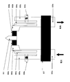
- This conventional electron gun will be described with reference to FIG.
- two pyrolytic graphites are obtained by cutting a LaB6 or CeB6 single crystal chip 801 having a conductivity and a work function for generating electrons in the vicinity of 2.6 eV along a plane perpendicular to the C-axis direction. It is made of a material sandwiched between 802a and 802b. This is held by metal supports 803a and 803b, and held by moderate pressure by the parts 804a and 804b constituting the spring. The spring force is adjusted by rotating the screws 806a and 806b for tightening from the supports 805a and 805b to change the amount of protrusion.
- the ends of the supports 805a and 805b are fixed to an alumina ceramic disc 807, and 805a and 805b are electrically insulated from each other.
- the legs of the supports 805a and 805b are in electrical contact with the electrical lead-in terminals 808a and 808b, and by flowing a current of several amperes, the pyrolytic graphite 802a and 802b are heated, and a single crystal chip of LaB6 or CeB6 801 is kept at a high temperature around 1500 ° C. and operated as a thermionic gun cathode or a thermal field emission cathode.
- the LaB6 or CeB6 single crystal chip is fixed with two pyrolytic graphites from both sides by springs, so the electron gun cathode structure is complicated and it is relatively difficult to align the center axis of electrons.
- a total of several tens to several hundred amperes on a high-voltage power supply of several tens kV for example, approximately -50 kV.
- the capacity of the high-voltage power supply is increased.
- an electric wire having a diameter of several millimeters or more is required.
- the above thickness is necessary, it is doubled for current heating, and several tens or more are required, and it becomes a power cable having a cross-sectional area of about tens of centimeters or more, and is mounted on a vibration isolator. Mechanical vibration was transmitted from the power cable to the multi-column, and a pattern could not be drawn with an accuracy of 1 nm or less.
- Patent Document 1 and Patent Document 2 disclose a technique for irradiating laser light in a non-contact manner from the front side or the back side of the tip portion of the electron gun cathode material, efficiently heating it, and extracting many electron beams. To do.
- JP-A-8-212952 Japanese Patent Laid-Open No. 6-181029
- an electron gun cathode material hexaboronated lanthanoid compounds such as LaB6 (LaB 6 ) and CeB6 (CeB 6 ) are often used. Generally used at high temperatures.
- an electron gun cathode for example, LaB6
- LaB6 has a large surface area of several square millimeters and is exposed as a whole.
- a lower temperature can be used as a result of applying the strong electric field.
- the temperature can be relatively low, such as 1700 K or lower, 1650 K, 1600 K, and the like, and sublimation of the material can be reduced.
- the whisker of sublimation deposits is formed on the surface of the anode / extraction electrode or the shape of the cathode material changes due to long-term use. Therefore, it is desired to further reduce sublimation and evaporation of the cathode material.
- the electron gun according to the present invention is a columnar electron gun cathode that emits electrons when heated, and covers the bottom and side surfaces of the electron gun cathode in the electron gun holding part at the tip, and holds the electron gun cathode.
- a holder made of a material that has electrical conductivity and hardly reacts with the electron gun cathode in a heated state, and has a shape that protrudes entirely toward the electron gun cathode holding portion.
- the gun cathode is characterized in that the tip portion is exposed and protrudes from the holder, and an electron is applied forward from the tip portion by applying an electric field to the tip portion.
- the electron gun cathode preferably has a flat surface at the tip, and emits electrons from the flat surface.
- the tip of the electron gun cathode is tapered.
- the electron gun cathode is preferably made of a material selected from one of hexaboronated lanthanoid compounds containing LaB6 or CeB6.
- the holder is made of rhenium.
- the holder has a concave portion for holding the electron gun cathode at a tip portion.
- the holder has a crack that passes through the concave portion from the tip side to the middle portion, and the electron gun cathode is sandwiched by the elastic force of the holder.
- the base is coupled to the optical waveguide on the base side opposite to the tip side that holds the electron gun cathode of the holder, and the electron gun cathode is heated through the holder by the light supplied through the optical waveguide. Is preferable.
- the holder has a crack extending from the distal end side to the intermediate portion, and sandwiches the electron gun cathode by the elastic force of the holder, and has a crack extending from the base side to the intermediate portion, It is preferable that the crack that sandwiches the optical waveguide and the electron gun cathode and the crack that sandwich the optical waveguide are spatially orthogonal in the axial direction of the holder by elastic force.
- An electron beam apparatus includes an electron gun, a beam control unit that extracts and directs electrons from the electron gun, and a target holding unit that holds a target irradiated with electrons from the beam control unit.
- the electron gun has a columnar electron gun cathode that emits electrons when heated, covers the bottom and side surfaces of the electron gun cathode, holds the electron gun cathode, and conducts electricity.
- a holder made of a material that does not easily react with the electron gun cathode in a heated state, and the electron gun cathode protrudes from the holder with a tip portion exposed, By applying an electric field to the tip portion, electrons are emitted forward from the tip portion.
- the electron beam apparatus includes an electron beam exposure apparatus and an electron beam inspection apparatus such as an electron microscope.
- the bottom surface and the side surface of the electron gun cathode are covered with the holder, and the tip of the electron gun cathode protrudes. Therefore, it is possible to extend the life of the electron gun by reducing the emission of electrons and electron gun cathode material from the side surface of the electron gun cathode.
- FIG. 1 is a diagram illustrating a configuration of an electron gun 100 according to the embodiment.
- the electron gun 100 employs a light heating method.
- light is light with high energy density, and is incident from one end portion (lower light incident end in the figure) of a cylindrical optical waveguide 102 made of sapphire or the like, and on the opposite side of the optical waveguide 102.
- the holder 103 installed at the end portion (tip portion).
- the holder 103 is composed of a conical portion on the distal end side of the cylindrical portion on the base side, and is composed of rhenium as a whole.
- a cylindrical recess is formed on the base side of the holder 103, and the tip of the optical waveguide 102 is accommodated therein.
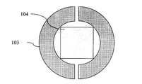
- the conical portion of the holder 103 has a truncated cone shape with a tip portion cut off, and a concave portion is formed on the tip surface thereof inward, and further passes through the concave portion and further toward the base side. A crack extending toward the surface is formed. Then, the electron gun cathode 104 is inserted into the recess from the tip side so as to spread the crack, and the electron gun cathode 104 is held by the elasticity of the holder 103.
- the light is introduced from the light source into the optical waveguide 102 by, for example, an optical fiber, is incident on the holder 103 and absorbed, and the electron gun cathode 104 is heated to a high temperature via the holder 103. Therefore, by adjusting the light intensity, it is possible to obtain conditions for emitting electrons from the electron gun cathode 104 into the vacuum.
- the light is, for example, light emitted from a semiconductor laser. Visible light is suitable for aligning the optical axis, but it is also possible to use ultraviolet rays to infrared rays.
- the optical waveguide 102 is a light propagation path, and the light incident from the incident end is totally reflected on the side surface and guided forward, and propagates to the holder 103 without being scattered.
- the optical waveguide 102 is also a support that mechanically supports the holder 103 and the electron gun cathode 104, and the electron gun cathode 104 has heat resistance that can withstand a high temperature (approximately 1500 ° C.) at which electron emission conditions are obtained. is necessary.
- the optical waveguide 102 has a function of an electron supply path to the electron gun cathode 104. This function as an electron supply path is a function necessary for supplying electrons emitted from the electron gun cathode 104 into the vacuum via the holder 103.
- Examples of materials suitable for the optical waveguide 102 include sapphire, ruby, diamond, and quartz glass that transmit light and have a high melting point.
- conductivity is added in order to provide an electron supply path for supplying emitted electrons from the electron gun cathode 104.
- a metal film 101 having a thickness of about several hundreds of nanometers is deposited on the surface of the optical waveguide 102 by vapor deposition or sputtering.
- an ion implantation technique on the surface layer of the optical waveguide 102, one kind of ion selected from bromine, nitrogen, oxygen, fluorine, aluminum, phosphorus, sulfur, chlorine, gallium, and arsenic is implanted. You may provide electroconductivity.
- electrons may be supplied to the electron gun cathode 104 by another conducting wire.
- the electron gun cathode 104 is provided with an electron supply terminal, and an electron gun power source is connected to the electron gun cathode 104 by an electric wire, and electrons emitted from the electron gun cathode 104 are supplied from the electron gun power source.
- sapphire is most suitable due to light transparency, heat resistance, and workability.
- sapphire is selected from the materials of sapphire, ruby, diamond, and quartz glass as the optical waveguide 102.
- the shape of the optical waveguide 102 is preferably a cylindrical shape having a diameter that can be easily incident from an optical fiber propagating from the light source to the optical waveguide 102. It is also possible to use a tapered conical shape that becomes thinner toward the tip. Further, the structure may be a structure that changes the material and shape, reflects light on the inner surface of a hollow metal tube, and propagates the light to the tip.
- the holder 103 is a heating element that receives and absorbs light, and is also a structure that supports the electron gun cathode 104. It must be made of a substance that can provide a protective function that does not chemically react with the electron gun cathode material LaB6 or CeB6 at the operating temperature (approximately 1500 ° C) as an electron gun, and rhenium, tantalum, carbon, etc. can be used. It is. However, rhenium has the least reaction with the electron gun cathode material at high temperatures, and rhenium is most suitable. Therefore, in the present embodiment, rhenium is used for the holder 103.
- electron gun cathode materials such as LaB6 and CeB6 can be easily combined with many substances excluding some substances such as rhenium, tantalum and graphite (carbon) at the operating temperature as an electron gun. This is due to the need to prevent chemical loss and alteration of the electron gun characteristics.
- the shape of the holder 103 is such that the base side is a cylinder having a diameter larger than the diameter of the optical waveguide 102, and has a hole (concave portion) into which the optical waveguide 102 is inserted and fitted at the end portion. It has a truncated cone shape, and has a hole (concave portion) into which the electron gun cathode 104 is inserted and fitted.
- the electron gun cathode 104 is selected from one material selected from hexaboronated lanthanoid compounds such as LaB6 or CeB6, which are materials that emit thermoelectrons or thermal field emission electrons at a high temperature.
- the lanthanoid is a generic name of 15 elements from the third (3A) group of the 6th period of the periodic table, up to 71th ruthenium Lu having similar chemical properties as typified by the lanthanum La of atomic number 57.
- the electron gun cathode 104 is preferably a single crystal. Further, the operating temperature of the electron gun cathode 104 being high (approximately 1500 ° C.) means that the work function of LaB6 or CeB6 is 2.6 eV, and a temperature at which thermionic emission is possible.
- An electron beam passage is opened in front of the tip of the electron gun cathode 104, and a suppressor electrode 105 is provided in the vicinity thereof.
- the suppressor electrode 105 suppresses electron emission from the side surface of the optical waveguide 102 at zero potential with respect to the electron gun cathode 104.
- an extraction electrode 106 is provided by opening an electron beam passage.
- the extraction electrode 106 is applied with a potential of about +3 kV to about +10 kV with respect to the electron gun cathode 104, and is applied to the vicinity of the upper surface of the tip of the 100 ⁇ m diameter cylinder of the electron gun cathode 104. It is injected toward the gun anode 107.
- the electron gun anode 107 is normally at a ground potential (0 V), and a voltage for accelerating an electron beam of minus several tens of kV (eg, minus 50 kV) is applied to the electron gun cathode 104 to give a kinetic energy of several tens of keV (eg, 50 keV).
- An electron beam 108 is obtained by applying the thermal field emission electrons.
- the electron gun cathode 104 has a potential of approximately minus 50 kV
- the extraction electrode 106 has a potential of approximately minus 47 kV to approximately minus 40 kV.
- the entire structure of FIG. 1 functions as the electron gun 100.
- the insulating base 109 is an alumina ceramic disk, and the optical waveguide 102 is fixed at the center of the disk.
- the insulating base 109 can insulate the suppressor electrode 105 and the optical waveguide 102, but the suppressor electrode 105 may have the same potential as the optical waveguide 102.
- the insulating base 110 has a larger diameter than the insulating base 109, holds the insulating base 109 from below, supports the optical waveguide 102 at the center, and provides the bases of the suppressor electrode 105 and the extraction electrode 106 outside the insulating base 109. They are concentrically held apart from each other.
- the insulating base 110 insulates the extraction electrode 106 and the optical waveguide 102 from each other.
- the conductive ring 112 is at the end of the optical waveguide 102, contacts the outer surface of the insulating base 109, and contacts the metal film 101 made of a conductive material on the outer surface of the optical waveguide 102.
- An electron beam acceleration power source is connected to the conductive ring 112 to supply electrons emitted from the electron gun cathode 104 through the metal film 101 of the optical waveguide 102 and the holder 103.
- FIG. 2A, 2B, and 2C show a connection configuration of the holder 103, the electron gun cathode 104, and the optical waveguide 102.
- FIG. 2A is a diagram illustrating the electron gun cathode 104 and the optical waveguide 102 with the holder 103 as a cross section
- FIG. 2B is a front view
- FIG. 2C is a side view.
- the holder 103 is provided with a crack 103a extending from the distal end side to the intermediate portion and a crack 103b extending from the base portion side to the intermediate portion. These cracks 103a and 103b differ in the direction of 90 degrees in the plane direction (vertical direction).
- the cracks 103a and 103b are spatially orthogonal with respect to the axial direction of the holder.
- a cylindrical hole (recess) into which the electron gun cathode 104 is inserted and fitted is provided at the tip, and a cylindrical hole (recess) into which the optical waveguide 102 is inserted and fitted at the end on the base side. Is provided. Since the electron gun cathode 104 and the optical waveguide 102 are slightly larger than the holes, the electron gun cathode 104 and the optical waveguide 102 are held by the elasticity of the holder 103 when inserted into the holes. 103.
- the electron gun cathode 104 is a 50 ⁇ m (micrometer) ⁇ 50 ⁇ m square column with a length of about 100 ⁇ m, and the corresponding hole is a round hole with a diameter of about 70 ⁇ m, and the tip of the electron gun cathode 104 protrudes about 10 ⁇ m. Is preferable.
- the holder 103 is divided into two parts by one crack, but a spring divided into three parts and four parts may be used.
- the electron gun cathode 104 has a quadrangular prism shape.
- FIG. 3 is a view as seen from the distal end side, and in this way, four corners are held in contact with the cylindrical hole of the holder 103.
- the reason why the electron gun cathode 104 is rectangular is that it is easier to manufacture.
- a plate-like LaB6 crystal is provided with a plurality of slits in the horizontal and vertical directions from the surface with a blade. If this is seen in a cross section parallel to one of the cut grooves, it becomes as shown in FIG. Then, as shown in FIG. 5B, an adhesive is injected into the cut groove and hardened. Thereafter, as shown in FIG.
- the blade is cut so as to cross the groove in a direction parallel to the surface (shown as a cut line) with a blade, as shown in FIG. 5 (d).
- a set of square pillars hardened with an agent is obtained.
- a large number of square columnar electron gun cathodes 104 shown in FIG. 5E can be obtained.
- the electron gun cathode 104 has, for example, a tip having a plane of about 50 ⁇ m ⁇ 50 ⁇ m and a length of about 100 ⁇ m. It is very difficult to process such a small electron gun cathode 104 with an ordinary lathe or the like. In addition, even when the blade is cut, it will fly away from the crystal substrate. By the processing method as described above, the small electron gun cathode 104 can be effectively manufactured.
- the crystal chip of LaB6 often has cracks. Chips with cracks often have unstable temperature characteristics when heated, and the temperature cannot be maintained in a steady state, so they tend to have unstable characteristics. Therefore, the position where the electron beam is emitted fluctuates and the radiation direction fluctuates angularly, and the electron gun characteristics tend to become unstable.
- the electron gun cathode 104 of the present embodiment has a size of 50 ⁇ m ⁇ 50 ⁇ m ⁇ 100 ⁇ m and a small volume as a crystal. For this reason, cracks hardly occur. Therefore, the temperature characteristics during heating are stable, the beam position is less changed, and the electron emission characteristics are extremely stable.
- a thermal field emission (TFE) type electron gun 100 that heats the electron gun cathode 104 and draws electrons by applying an electric field to the electron gun cathode 104 is used.
- An electric field of about 0.5 to 1.0 ⁇ 10 6 V / cm is applied and the temperature is set to about 1650-1700K.
- LaB6 or CeB6 is used as the material of the electron gun cathode 104, and this is held by a rhenium holder 103. At such a temperature, rhenium hardly reacts with LaB6 or CeB6, and therefore it is possible to effectively prevent the electron gun cathode 104 from being altered by a chemical reaction.
- the tip of the electron gun cathode 104 is a plane of about 50 ⁇ m ⁇ 50 ⁇ m in plane, and only the tip protrudes from the rhenium holder 103.
- the protruding amount is set to 2 to 15 ⁇ m.
- most of the side surface of the electron gun cathode 104 having a length of about 100 ⁇ m is covered with the holder 103, so that sublimation of electrons and materials from the side surface of the electron gun cathode 104 can be reduced. .
- the electron irradiation from the side surface of the electron gun cathode 104 is small, and extra heating to the peripheral members can be minimized.
- the number of electrons emitted from the whole including the electron gun cathode 104 and the tip side surface can be reduced, and the sublimation and evaporation of the material can be reduced.
- Conventional sublimation area of several square millimeters is 2500 square microns, and the area ratio is less than 1/200. Therefore, the formation of whisker of sublimation deposits on the surfaces of the electron gun anode 107 and the extraction electrode 106 can be suppressed, and the time until the discharge occurs can be lengthened and the life can be extended.
- the side surface of the electron gun cathode material can be suppressed from thinning and the initial electron extraction state can be maintained for a long time. Furthermore, if it is LaB6, it can suppress that a boron (B) atom or a lanthanum (La) lanthanum atom escapes from the crystal
- the holder 103 made of rhenium has a base having a diameter of about 1000 ⁇ m, a tip having a diameter of about 100 ⁇ m, and a length of about 1 mm to 2 mm.
- the consumption due to the use of the electron gun cathode 104 is relatively small. However, it is inevitable that the electron gun cathode 104 is consumed by use. In the present embodiment, for example, as shown in FIG. 7, the volume of the electron gun cathode 104 gradually decreases from the tip surface.
- Fig. 7 (a) schematically shows an example after the start of use
- Fig. 7 (c) schematically after three years.
- the protruding amount of the electron gun cathode 104 is large, it is not preferable because the emission and sublimation of electrons from the side surface increase accordingly.
- consumption due to use is unavoidable, and when the tip of the electron gun cathode 104 enters the hole of the holder 103 and becomes as shown in FIG. Therefore, in order to extend the life as much as possible and reduce the formation of whiskers on the extraction electrode 106 and the like, it is preferable to set the protrusion amount of the electron gun cathode 104 from the holder 103 at the start of use to about 2 to 15 ⁇ m.
- the thickness is preferably about 10 ⁇ m.
- the flat surface of the tip is set to about 50 ⁇ 50 ⁇ m, but high luminance can be achieved by reducing the area.
- a variable shaped beam, cell projection beam (CP) or the like needs to irradiate a certain area uniformly. This is said to require uniform irradiation. It is also said that a large emittance is necessary.
- the holder 103 made of rhenium has a shape that tapers sharply toward the tip.
- the electron gun cathode 104 is held by covering the bottom and side surfaces of the electron gun holding portion at the tip. Therefore, as shown in FIG. 14, the electric field around the electron gun cathode has an equipotential line having a sharp mountain shape corresponding to the tip shape of the holder 103, and a strong electric field is applied to the tip portion. Therefore, the emission of the electron beam from the tip of the electron gun cathode 104 is promoted.
- the electron gun cathode 104 having a flat tip as shown in the above-described embodiment is suitable for a variable shaped beam or cell projection beam (CP) exposure apparatus.
- CP cell projection beam
- the electron gun cathode 104 having a sharp tip may be employed.
- the cathode having such a shape is also suitable for an electron beam inspection apparatus such as a scanning electron microscope (SEM).
- SEM scanning electron microscope
- electron beam inspection apparatuses such as an electron beam exposure apparatus and an electron microscope are collectively referred to as an electron beam apparatus.
- an electron beam emitted from an electron gun is irradiated onto a sample as a spot and scanned in the same manner as in an electron beam exposure apparatus. Then, secondary electrons generated from the sample are detected by a detector, and the detection result is imaged.
- the electron gun of this embodiment can also be applied to an electron beam inspection apparatus such as a transmission electron microscope (TEM).
- TEM transmission electron microscope
- FIG. 8 shows the shape of the columnar electron gun cathode 104 embedded in the tip of the holder 103 having a pointed tip. That is, the electron gun cathode 104 is inserted at the tip of the holder 103, but the diameter becomes smaller as the tip of the electron gun cathode 104 is conical first.
- the amount of sublimation and evaporation from the electron gun cathode 104 can be reduced, and the amount of electron gun cathode material adhering to the extraction electrode 106 and the electron gun anode 107 can be reduced.
- the lifetime determined by the discharge caused by the growth of the whisker can be extended.
- FIG. 9 shows a tungsten filament heating type electron gun.
- FIG. 9A shows the front, and
- FIG. 9B shows the side.
- the holder 103 is the same as that described above on the distal end side, but the base side is half-cut out and has a semi-cylindrical shape.
- the upper ends of a pair of tungsten filaments 121 arranged in an inverted V shape on the plane of the semi-cylinder are spot-welded in common.
- the paired lower ends of the paired tungsten filaments 121 are spot welded to a pair of metal rods 122 fixed to the ceramic substrate 123, respectively. Then, by supplying electric power between the pair of metal rods 122, the tungsten filament 121 is heated, and the electron gun cathode 104 is heated to a predetermined temperature via the holder 103 by this heat.
- the metal rod 122, the tungsten filament 121, and the electron gun cathode 104 are all maintained at the same cathode potential (DC voltage), and electrons are emitted from the electron gun cathode 104, which is the same as in the above-described embodiment. .
- FIG. 10 shows a schematic configuration of an electron beam exposure apparatus using the electron gun 100 described above.
- the lens barrel 204 is a hermetically sealed cylinder, and an electron gun chamber 201 is partitioned and formed by a partition wall 202 at the top.
- a lens / deflection functioning as a beam control unit including a coil, a magnetic lens, and the like for deflecting, shaping, and converging the electron beam 205 extracted from the electron gun 100
- An optical system 203 is arranged inside the lens barrel 204.
- a target chamber 210 is disposed below the lens barrel 204, and a target 206, which is a substrate (wafer) drawn thereon, is placed thereon.
- the electron beam 205 drawn out from the electron gun 100 is controlled to converge at an arbitrary position of the target 206, and drawing by the electron beam is performed.
- the ion pump 207 exhausts the inside of the electron gun chamber 201
- the turbo molecular pump 208 exhausts the inside of the lens barrel 204
- the turbo molecular pump 209 exhausts the inside of the target chamber 210, and each maintains a desired vacuum state.
- This apparatus includes a secondary electron or backscattered electron detector 211, so that not only electron beam drawing but also image observation can be performed by scanning the electron beam. It can also be used as an electron beam inspection apparatus for inspecting an image of a wafer or a mask substrate.
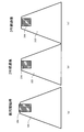
- Multi-column configuration The electron gun of this embodiment can be suitably applied to a multi-column electron beam exposure apparatus.
- a multi-column electron beam exposure apparatus a plurality of single column elements having a thickness of about 15 mm to about 50 mm, for example, are arranged two-dimensionally in the number of several tens or more (for example, 30 to 250 or more), A multi-column group that irradiates a plurality of electron beams onto one wafer is formed. With such a configuration, high-speed exposure processing can be performed.
- FIG. 11 shows a diagram of a multi-column electron beam drawing apparatus. 89 fine columns having a column element of about 25 mm in diameter as a unit are arranged on a 300 mm wafer. A schematic configuration of one single column element 301 is shown.
- the electron beam emitted from the electron gun 304 is shaped into a rectangle by the first rectangular aperture 305 and imaged on the second rectangular aperture or CP mask 308 by the lens / deflection optical system 306 in the previous stage.
- the position of the electron beam on the second rectangular aperture or CP mask 308 is reshaped to a beam of the intended size or shape by a beam deflector.
- lens / deflection optical system 309 in the subsequent stage deflects and forms an image at an appropriate position on the wafer located below.
- These lens / deflection optical systems 306 and 309 function as a beam control unit, and are further constituted by a magnetic lens 307 when further disassembled.
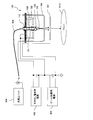
- FIG. 12 is a configuration diagram of the light heating type electron gun of this embodiment and a control unit of the electron gun.
- the electron beam accelerating power source 403 is a high voltage generating unit that supplies a high voltage of minus several tens kV (for example, approximately ⁇ 50 kV) to the electron gun cathode 104.
- the voltage is supplied to the metal on the surfaces of the conductive ring 112 and the optical waveguide 102. Application is made to the electron gun cathode 104 through the film 101.
- the extraction electric field power source 402 generates a voltage of plus several kV (approximately +3 kV to +10 kV) with respect to the electron beam acceleration power source 403, and applies the voltage to the extraction electrode 106.
- the light source unit 504 is a unit that generates light and adjusts the intensity of light by the semiconductor laser and its control unit.
- the optical fiber 505 is an optical transport path that guides the light from the light source unit 504 to the optical waveguide 102.
- Each optical fiber 505 has a thickness of about 250 microns and can be bundled by several tens or more. The thickness is about 2.5 mm in diameter.
- the optical fiber 505 is an insulator such as glass or plastic, and unlike an electric wire, it does not need to be specially insulated. Therefore, the optical fiber 505 is directly applied to a minus several tens kV (for example, approximately -50 kV) high-voltage electron gun unit. Can be introduced.
- the conventional heating method uses a thick conductive cable with a diameter of several centimeters or more that is high-voltage insulated for current heating, so it is heavy and rigid and hard, so floor vibration is transmitted and the electron optical column vibrates. As a result, the beam vibrates and the drawing accuracy deteriorates.
- the energy of light input to the electron gun 100 is radiated as radiant heat of these members and conduction heat through the optical waveguide 102 by setting the holder 103 and the electron gun cathode 104 to a high temperature around 1500 ° C. Therefore, the light intensity is adjusted so that the temperature of the electron gun cathode 104 becomes a constant value around 1500 ° C.
- the intensity of the electron beam flowing into the light source is measured, and the light source unit 504 is controlled so as to keep the measured value constant.
- the output of the semiconductor laser is controlled so as to keep it constant.
- the optical fiber 505 is separated from the high-voltage system, and the handling becomes easy.
- the cable for transmitting the light energy is thin, lightweight, and the rigidity is small, so that the floor vibration is hardly transmitted, so that drawing with high accuracy is possible.
- the problem with the multi-column electron gun is the heat generated by the electron gun cathode.
- the number of multi-column electron guns is multiplied by several watts, which is a calorific value determined by the product of the area of the high temperature portion and the fourth power of the temperature. Value, that is, a calorific value of several hundred watts.
- the degree of vacuum of the electron gun chamber 201 may deteriorate. In order to avoid the deterioration of the degree of vacuum, it is effective to reduce the surface area of the holder 103.
- the calorific value can be reduced to about a quarter, the calorific value can be reduced to 100 watts or less, and the degree of vacuum can be reduced.
- the holder 103 has a shape in which the base portion is short and the thin portion is long.
- the holder may be configured with a thin wire within a range in which the entire structure is not changed.
- the luminance is 3 to 6 ⁇ 10 6 A / cm 2 steradian when applied to an electron beam lithography apparatus, A value of 7 to 10 mrad um is obtained as the electron gun emittance representing the irradiation uniformity of the rectangular aperture, and the lifetime is 2 to 3 years, so that it can be used as an ideal electron gun.
- This can greatly contribute to the practical application of the electron beam drawing apparatus. Further, it is possible to greatly contribute to the improvement of the scanning transmission electron microscope and the electron beam inspection apparatus.
- the holder 103 is formed of rhenium as a whole. This is to suppress a chemical reaction with the electron gun cathode 104 made of LaB6 or the like. Therefore, if the part of the holder 103 that contacts the electron gun cathode is formed of rhenium, the other part of the holder 103 may be formed of another material, for example, highly rigid tungsten, tantalum, molybdenum, or the like.
Landscapes
- Chemical & Material Sciences (AREA)
- Analytical Chemistry (AREA)
- Engineering & Computer Science (AREA)
- Nanotechnology (AREA)
- Physics & Mathematics (AREA)
- Crystallography & Structural Chemistry (AREA)
- Optics & Photonics (AREA)
- Theoretical Computer Science (AREA)
- Condensed Matter Physics & Semiconductors (AREA)
- General Physics & Mathematics (AREA)
- Manufacturing & Machinery (AREA)
- Mathematical Physics (AREA)
- Electron Sources, Ion Sources (AREA)
- Electron Beam Exposure (AREA)
Abstract
Description
図1は、実施形態に係る電子銃100の構成を示す図である。この例では、電子銃100は、光加熱方式を採用している。
ここで、単一のスポット(点状)ビームを用いるのであれば、電子銃陰極104の先端を尖らせたものを採用することもできる。このような形状の陰極は、走査型電子顕微鏡(SEM)のような電子ビーム検査装置にも好適である。本明細書では、電子ビーム露光装置、電子顕微鏡などの電子ビーム検査装置を総称して電子ビーム装置という。
図10には、上述した電子銃100を利用した電子ビーム露光装置の概略構成が示してある。鏡筒204は密閉状の円筒であり、上部に電子銃室201が仕切り壁202によって仕切り形成されている。鏡筒204の内部には、電子銃100から引き出された電子ビーム205を偏向、整形、収束などをするために、コイル、磁気レンズなどをから構成される、ビーム制御部として機能するレンズ・偏向光学系203が配置されている。そして、鏡筒204の下方には、ターゲット室210が配置されており、ここに描画される基板(ウェハ)であるターゲット206が載置されている。
本実施形態の電子銃は、マルチコラム電子ビーム露光装置に好適に適用できる。このマルチコラム電子ビーム露光装置は、たとえば略15mmから略50mm程度の太さの単一コラムエレメントを、2次元的に数十本以上(たとえば30本から250本以上)という数で複数個並べ、1枚のウェハ上に電子ビームを複数照射するマルチコラム群を構成する。このような構成によって、高速露光処理が可能となる。
上述のように、電子銃の加熱に光を用いることが好適である。図12は、本実施形態の光加熱式の電子銃と、その電子銃の制御部の構成図である。
Claims (10)
- 加熱されることによって電子を放出する柱形の電子銃陰極と、
先端の電子銃保持部において前記電子銃陰極の底面および側面を覆い電子銃陰極を保持するとともに、電気伝導性を有し、加熱された状態で前記電子銃陰極と反応し難い材料で構成され、前記電子銃陰極保持部に向かって全体が先細り突き出る形状を有する保持具と、
を含み、
前記電子銃陰極は、先端部が露出して前記保持具から突出しており、前記先端部に電界を印加することにより前記先端部から電子を前方に向けて放出することを特徴とする電子銃。 - 請求項1に記載の電子銃であって、
前記電子銃陰極は、その先端に平坦面を有し、この平坦面から電子を放出することを特徴とする電子銃。 - 請求項1に記載の電子銃であって、
前記電子銃陰極の先端部は、先細り状となっていることを特徴とする電子銃。 - 請求項1に記載の電子銃において、
前記電子銃陰極は、LaB6またはCeB6を含む6硼素化ランタノイド化合物の中から1種類を選択した材料からなることを特徴とする電子銃。 - 請求項1に記載の電子銃において、
前記保持具は、レニウムで構成されることを特徴とする電子銃。 - 請求項1に記載の電子銃において、
前記保持具は、先端部に前記電子銃陰極を保持する凹部を有することを特徴とする電子銃。 - 請求項4に記載の電子銃において、
前記保持具は、先端側から中間部まで前記凹部を通過する割れ目を有しており、保持具の弾性力によって、前記電子銃陰極を挟持することを特徴とする電子銃。 - 請求項1に記載の電子銃において、
前記保持具の前記電子銃陰極を保持する先端側と反対の基部側で光導波路と結合され、前記電子銃陰極は、前記光導波路を介し供給される光によって前記保持具を介し加熱されることを特徴とする電子銃。 - 請求項8に記載の電子銃において、
前記保持具は、先端側から中間部まで至る割れ目を有し、保持具の弾性力によって、前記電子銃陰極を挟持するとともに、
基部側から中間部に至る割れ目を有し、保持具の弾性力によって、前記光導波路を挟持し、
前記電子銃陰極を挟持する割れ目と、前記光導波路を挟持する割れ目が、前記保持具の軸に関し空間的に直交していることを特徴とする電子銃。 - 電子銃と、電子銃から電子を引き出すとともに方向付けをするビーム制御部と、このビーム制御部からの電子が照射されるターゲットを保持するターゲット保持部を有する電子ビーム装置であって、
前記電子銃は、
加熱されることによって電子を放出する柱形の電子銃陰極と、
この電子銃陰極の底面および側面を覆い電子銃陰極を保持するとともに、電気伝導性を有し、加熱された状態で前記電子銃陰極と反応し難い材料で構成された保持具と、
を含み、
前記電子銃陰極は、先端部が露出して前記保持具から突出しており、前記先端部に電界を印加することにより前記先端部から電子を前方に向けて放出すること特徴とする電子ビーム装置。
Priority Applications (6)
| Application Number | Priority Date | Filing Date | Title |
|---|---|---|---|
| CN201180068539.5A CN103392216B (zh) | 2011-02-25 | 2011-02-25 | 电子枪及电子束装置 |
| PCT/JP2011/054377 WO2012114521A1 (ja) | 2011-02-25 | 2011-02-25 | 電子銃および電子ビーム装置 |
| KR1020137024916A KR20140044310A (ko) | 2011-02-25 | 2011-02-25 | 전자총 및 전자빔 장치 |
| JP2013500809A JP5525104B2 (ja) | 2011-02-25 | 2011-02-25 | 電子銃および電子ビーム装置 |
| EP11859058.7A EP2680294B1 (en) | 2011-02-25 | 2011-02-25 | Electron gun and electron beam device |
| US14/000,988 US9070527B2 (en) | 2011-02-25 | 2011-02-25 | Electron gun and electron beam device |
Applications Claiming Priority (1)
| Application Number | Priority Date | Filing Date | Title |
|---|---|---|---|
| PCT/JP2011/054377 WO2012114521A1 (ja) | 2011-02-25 | 2011-02-25 | 電子銃および電子ビーム装置 |
Publications (1)
| Publication Number | Publication Date |
|---|---|
| WO2012114521A1 true WO2012114521A1 (ja) | 2012-08-30 |
Family
ID=46720336
Family Applications (1)
| Application Number | Title | Priority Date | Filing Date |
|---|---|---|---|
| PCT/JP2011/054377 WO2012114521A1 (ja) | 2011-02-25 | 2011-02-25 | 電子銃および電子ビーム装置 |
Country Status (6)
| Country | Link |
|---|---|
| US (1) | US9070527B2 (ja) |
| EP (1) | EP2680294B1 (ja) |
| JP (1) | JP5525104B2 (ja) |
| KR (1) | KR20140044310A (ja) |
| CN (1) | CN103392216B (ja) |
| WO (1) | WO2012114521A1 (ja) |
Cited By (3)
| Publication number | Priority date | Publication date | Assignee | Title |
|---|---|---|---|---|
| WO2019181820A1 (ja) * | 2018-03-19 | 2019-09-26 | 株式会社Param | 電子銃 |
| JP2022548454A (ja) * | 2019-09-23 | 2022-11-21 | フリーメルト エービー | 電子銃カソード技術 |
| US11915921B2 (en) | 2020-04-21 | 2024-02-27 | Denka Company Limited | Electron source, method for manufacturing same, emitter, and device including same |
Families Citing this family (15)
| Publication number | Priority date | Publication date | Assignee | Title |
|---|---|---|---|---|
| JP6420998B2 (ja) * | 2014-09-03 | 2018-11-07 | 株式会社ニューフレアテクノロジー | 電子銃装置 |
| WO2018047228A1 (ja) * | 2016-09-06 | 2018-03-15 | 株式会社日立ハイテクノロジーズ | 電子源および電子線照射装置 |
| US10141155B2 (en) | 2016-12-20 | 2018-11-27 | Kla-Tencor Corporation | Electron beam emitters with ruthenium coating |
| CN107068528B (zh) * | 2016-12-28 | 2018-08-24 | 中国电子科技集团公司第十八研究所 | 电子束聚焦线圈在焊接真空室内的电子枪保护装置 |
| JP6636472B2 (ja) * | 2017-02-28 | 2020-01-29 | 株式会社日立ハイテクノロジーズ | 電子源およびそれを用いた電子線装置 |
| CN109698102B (zh) * | 2017-10-20 | 2021-03-09 | 中芯国际集成电路制造(上海)有限公司 | 电子枪、掩膜版制备方法及半导体装置 |
| EP3794626A1 (en) * | 2018-03-23 | 2021-03-24 | Freemelt Ab | Cathode assembly for electron gun |
| CN108437472B (zh) * | 2018-03-29 | 2024-04-05 | 天津清研智束科技有限公司 | 一种增材制造装置及增材制造方法 |
| WO2019185053A1 (zh) * | 2018-03-29 | 2019-10-03 | 天津清研智束科技有限公司 | 射线发生装置、增材制造装置及增材制造方法 |
| US11508544B2 (en) * | 2018-09-25 | 2022-11-22 | Hitachi High-Tech Corporation | Thermoelectric field emission electron source and electron beam application device |
| JP7137002B2 (ja) * | 2019-04-18 | 2022-09-13 | 株式会社日立ハイテク | 電子源、及び荷電粒子線装置 |
| US11380511B2 (en) * | 2020-03-24 | 2022-07-05 | Fei Company | Charged particle beam source |
| JP6762635B1 (ja) * | 2020-04-16 | 2020-09-30 | 株式会社Photo electron Soul | 電子銃、電子線適用装置、および、電子ビームの射出方法 |
| JPWO2021215335A1 (ja) * | 2020-04-21 | 2021-10-28 | ||
| JP2022130056A (ja) * | 2021-02-25 | 2022-09-06 | 株式会社ニューフレアテクノロジー | 電子銃の陰極機構、電子銃、及び電子ビーム描画装置 |
Citations (8)
| Publication number | Priority date | Publication date | Assignee | Title |
|---|---|---|---|---|
| JPS57196445A (en) * | 1981-05-26 | 1982-12-02 | Ibm | Forming electron beam generator |
| JPS6332846A (ja) * | 1986-07-25 | 1988-02-12 | Tadao Suganuma | 電子銃 |
| JPH0298921A (ja) * | 1988-10-05 | 1990-04-11 | Fujitsu Ltd | 電子銃およびその製造方法および該電子銃を備えた露光装置および該露光装置を用いる半導体装置の製造方法 |
| JPH03274632A (ja) * | 1990-03-23 | 1991-12-05 | Hitachi Medical Corp | 電子銃 |
| JPH06181029A (ja) | 1992-12-14 | 1994-06-28 | Mitsubishi Heavy Ind Ltd | 電子銃の陰極レーザ加熱機構 |
| JPH0850873A (ja) * | 1994-08-08 | 1996-02-20 | Nec Kansai Ltd | 熱陰極構体およびその熱陰極構体を用いた電子ビ ーム加工装置 |
| JPH08212952A (ja) | 1995-02-06 | 1996-08-20 | Natl Res Inst For Metals | レーザー照射型電子銃 |
| US6828996B2 (en) * | 2001-06-22 | 2004-12-07 | Applied Materials, Inc. | Electron beam patterning with a heated electron source |
Family Cites Families (11)
| Publication number | Priority date | Publication date | Assignee | Title |
|---|---|---|---|---|
| JPS5514646A (en) * | 1978-07-17 | 1980-02-01 | Toshiba Corp | Electron gun |
| JPS5865004U (ja) | 1981-10-26 | 1983-05-02 | 三菱電線工業株式会社 | イメ−ジガイド |
| EP0084216A1 (en) | 1981-10-26 | 1983-07-27 | Dainichi-Nippon Cables, Ltd. | Image guide |
| JPS62241254A (ja) | 1986-04-10 | 1987-10-21 | Ushio Inc | 放電灯 |
| JPH0518832Y2 (ja) | 1987-05-08 | 1993-05-19 | ||
| JPH05128963A (ja) * | 1991-04-18 | 1993-05-25 | Hitachi Medical Corp | 電子銃 |
| DE69621803T2 (de) | 1996-10-02 | 2003-01-16 | Advantest Corp | Elektronenstrahlerzeugende Vorrichtung |
| JP2000235839A (ja) | 1999-02-16 | 2000-08-29 | Hitachi Ltd | 電子線応用装置 |
| JP2003217448A (ja) | 2002-01-21 | 2003-07-31 | Sony Corp | 陰極線管用電子銃の組立装置 |
| US6556651B1 (en) | 2002-01-25 | 2003-04-29 | Photoelectron Corporation | Array of miniature radiation sources |
| JP5305701B2 (ja) | 2008-03-21 | 2013-10-02 | 株式会社アドバンテスト | 電子ビーム露光装置及び電子ビーム露光方法 |
-
2011
- 2011-02-25 CN CN201180068539.5A patent/CN103392216B/zh not_active Expired - Fee Related
- 2011-02-25 EP EP11859058.7A patent/EP2680294B1/en not_active Not-in-force
- 2011-02-25 WO PCT/JP2011/054377 patent/WO2012114521A1/ja active Application Filing
- 2011-02-25 JP JP2013500809A patent/JP5525104B2/ja active Active
- 2011-02-25 US US14/000,988 patent/US9070527B2/en not_active Expired - Fee Related
- 2011-02-25 KR KR1020137024916A patent/KR20140044310A/ko not_active Application Discontinuation
Patent Citations (8)
| Publication number | Priority date | Publication date | Assignee | Title |
|---|---|---|---|---|
| JPS57196445A (en) * | 1981-05-26 | 1982-12-02 | Ibm | Forming electron beam generator |
| JPS6332846A (ja) * | 1986-07-25 | 1988-02-12 | Tadao Suganuma | 電子銃 |
| JPH0298921A (ja) * | 1988-10-05 | 1990-04-11 | Fujitsu Ltd | 電子銃およびその製造方法および該電子銃を備えた露光装置および該露光装置を用いる半導体装置の製造方法 |
| JPH03274632A (ja) * | 1990-03-23 | 1991-12-05 | Hitachi Medical Corp | 電子銃 |
| JPH06181029A (ja) | 1992-12-14 | 1994-06-28 | Mitsubishi Heavy Ind Ltd | 電子銃の陰極レーザ加熱機構 |
| JPH0850873A (ja) * | 1994-08-08 | 1996-02-20 | Nec Kansai Ltd | 熱陰極構体およびその熱陰極構体を用いた電子ビ ーム加工装置 |
| JPH08212952A (ja) | 1995-02-06 | 1996-08-20 | Natl Res Inst For Metals | レーザー照射型電子銃 |
| US6828996B2 (en) * | 2001-06-22 | 2004-12-07 | Applied Materials, Inc. | Electron beam patterning with a heated electron source |
Non-Patent Citations (2)
| Title |
|---|
| "Edectronllon beam handbook", 28 October 1998, JAPAN SOCIETY FOR THE PROMOTION OF SCIENCE |
| See also references of EP2680294A4 |
Cited By (4)
| Publication number | Priority date | Publication date | Assignee | Title |
|---|---|---|---|---|
| WO2019181820A1 (ja) * | 2018-03-19 | 2019-09-26 | 株式会社Param | 電子銃 |
| JP2022548454A (ja) * | 2019-09-23 | 2022-11-21 | フリーメルト エービー | 電子銃カソード技術 |
| JP7294754B2 (ja) | 2019-09-23 | 2023-06-20 | フリーメルト エービー | 金属3dプリンタ |
| US11915921B2 (en) | 2020-04-21 | 2024-02-27 | Denka Company Limited | Electron source, method for manufacturing same, emitter, and device including same |
Also Published As
| Publication number | Publication date |
|---|---|
| CN103392216A (zh) | 2013-11-13 |
| EP2680294A4 (en) | 2014-10-08 |
| JPWO2012114521A1 (ja) | 2014-07-07 |
| EP2680294A1 (en) | 2014-01-01 |
| US9070527B2 (en) | 2015-06-30 |
| KR20140044310A (ko) | 2014-04-14 |
| CN103392216B (zh) | 2016-10-05 |
| US20140055025A1 (en) | 2014-02-27 |
| EP2680294B1 (en) | 2015-09-09 |
| JP5525104B2 (ja) | 2014-06-18 |
Similar Documents
| Publication | Publication Date | Title |
|---|---|---|
| JP5525104B2 (ja) | 電子銃および電子ビーム装置 | |
| JP4878311B2 (ja) | マルチx線発生装置 | |
| US7868850B2 (en) | Field emitter array with split gates and method for operating the same | |
| KR100766907B1 (ko) | 마이크로 집속 수준의 전자빔 발생용 탄소나노튜브 기판분리형 방사선관 시스템 | |
| KR102301555B1 (ko) | 루테늄 코팅을 가진 전자 빔 이미터 | |
| JP2007265981A5 (ja) | ||
| US6903499B2 (en) | Electron gun and a method for using the same | |
| Jarvis et al. | Emittance measurements of electron beams from diamond field emitter arrays | |
| US7556749B2 (en) | Electron source | |
| JP6002989B2 (ja) | 電子銃 | |
| JP4792404B2 (ja) | 電子源の製造方法 | |
| TW202013410A (zh) | 用於具有一擴散障壁之電子發射器之金屬保護層 | |
| JP2007287401A (ja) | 導電性針およびその製造方法 | |
| JP5709922B2 (ja) | 電子銃および電子ビーム装置 | |
| EP1744343B1 (en) | Carbon based field emission cathode and method of manufacturing the same | |
| JP2011181339A (ja) | 電子銃およびマルチコラム電子ビーム装置。 | |
| JP4032057B2 (ja) | 電子源の製造方法 | |
| Kirkpatrick et al. | Measurements of vacuum field emission from bio-molecular and semiconductor-metal eutectic composite microstructures | |
| KR101227258B1 (ko) | 탄소나노튜브 팁의 다중 배열을 이용하여 x-선 발생을 위한 3극관 냉음극 전자원 | |
| Choi et al. | Development of diamond field-emitter arrays for free-electron lasers | |
| JP2005332677A (ja) | 電子源の製造方法と使用方法 | |
| Zhang et al. | New applications for ultra-high brightness LaB 6 nanowire cathode | |
| KR20200076641A (ko) | 그래핀 필름을 포함하는 냉음극 및 이를 이용한 전자총 | |
| Ganter et al. | Low emittance gun project based on field emission | |
| JP2008293879A (ja) | X線源およびx線検査装置 |
Legal Events
| Date | Code | Title | Description |
|---|---|---|---|
| 121 | Ep: the epo has been informed by wipo that ep was designated in this application |
Ref document number: 11859058 Country of ref document: EP Kind code of ref document: A1 |
|
| ENP | Entry into the national phase |
Ref document number: 2013500809 Country of ref document: JP Kind code of ref document: A |
|
| NENP | Non-entry into the national phase |
Ref country code: DE |
|
| WWE | Wipo information: entry into national phase |
Ref document number: 2011859058 Country of ref document: EP |
|
| ENP | Entry into the national phase |
Ref document number: 20137024916 Country of ref document: KR Kind code of ref document: A |
|
| WWE | Wipo information: entry into national phase |
Ref document number: 14000988 Country of ref document: US |